Embed Size (px)
Citation preview
PHYSICAL REVIEW B 99, 165428 (2019)
Impact of device geometry on electron and phonon transport in graphene nanorings
M. Saiz-Bretín,1,2 L. Medrano Sandonas,2,3 R. Gutierrez,2 G. Cuniberti,2,3,4 and F. Domínguez-Adame1
1GISC, Departamento de Física de Materiales, Universidad Complutense, E-28040 Madrid, Spain2Institute for Materials Science, TU Dresden, 01062 Dresden, Germany
3Center for Advancing Electronics Dresden, TU Dresden, 01062 Dresden, Germany4Dresden Center for Computational Materials Science, TU Dresden, 01062 Dresden, Germany
(Received 12 February 2019; published 26 April 2019)
Recent progress in nanostructuring of materials opens up possibilities to achieve more efficient thermoelectricdevices. Nanofilms, nanowires, and nanorings may show increased phonon scattering while keeping goodelectron transport, two of the basic ingredients for designing more efficient thermoelectric systems. Here weargue that graphene nanorings attached to two leads meet these two requirements. Using a density-functionalparametrized tight-binding method combined with Green’s function technique, we show that the lattice thermalconductance is largely reduced as compared to that of graphene nanoribbons. At the same time, numericalcalculations based on the quantum transmission boundary method, combined with an effective transfer matrixmethod, predict that the electric properties are not considerably deteriorated, leading to an overall remarkablethermoelectric efficiency. We conclude that graphene nanorings can be regarded as promising candidates fornanoscale thermoelectric devices.
DOI: 10.1103/PhysRevB.99.165428
I. INTRODUCTION
Exploration of new materials and novel physical mecha-nisms for heat-to-electricity conversion lies at the heart ofthermoelectricity research. The thermoelectric efficiency ofmaterials and devices can be quantified by the dimensionlessfigure of merit ZT = σS2T/κ [1]. Here S stands for theSeebeck coefficient, and σ and κ are the electrical and thermalconductance at temperature T , respectively. Although the fig-ure of merit has formally no upper bound, values of ZT largerthan 3 are usually considered as necessary for widespreadapplications. Bulk materials are, however, usually well belowthis threshold. One obvious strategy for improving ZT isto reduce the thermal conductivity κ , while maximizing thepower factor σS2. However, the unfavorable interdependenceof S, σ , and κ in three-dimensional (3D) systems is themain cause of the low efficiency of current thermoelectricdevices compared to other energy-conversion technologies. Ingeneral, both electrons and phonons can contribute to the heatcurrent through a system subjected to a temperature gradient.Thus, the thermal conductance is split as κ = κel + κph. In thisregard, reducing the phonon contribution κph by increasingphonon scattering is an advantageous strategy to enhance ZT .This approach might be especially relevant when the electrondensity is low, as occurs in semiconductors and insulators,because the electron contribution κel is expected to be small.
It is frequently believed that phonon mean free paths �ph
are much longer than those of electrons �el. Miniaturization ofmaterials was predicted long ago to exploit this difference inorder to achieve a significant reduction of the phonon thermalconductivity while maintaining good electric properties [2,3],provided that their size is larger than �el but smaller than �ph.Furthermore, quantum effects allow nanodevices to overcomethe limitations stemming from the classical Wiedemann-Franz
law. For instance, sharp resonances in the electron transmis-sion (such as Fano line shapes) make the ratio σ/κel increasewell above the Wiedemann-Franz limit [4–11]. The combina-tion of these two factors, namely reduced �ph and enhancedσ/κel, explains why nanometer-sized objects may exhibitvalues of ZT unachievable with bulk materials [12–17].
Graphene is a paradigmatic example of a two-dimensionalmaterial whose thermoelectric efficiency can be signif-icantly improved after nanostructuring or functionaliza-tion. Graphene nanoribbons with rough edges [18], hy-drogen passivation [19], patterning [20–23], and hybridgraphene/hexaboron nitride superlattices [24] display a sub-stantial reduction of the lattice thermal conductivity. Theinsertion of bends, corners, and other structural modificationsin the phonon paths yields even lower thermal conductivity.For instance, arrays of nanopores [25] and double bends [26]drastically reduce the phonon contribution κph in graphenenanoribbons. The reduction of the thermal conductivity afterintroducing obstacles, however, does not always improve ther-moelectric efficiency since electrical conduction can be dete-riorated as well. This has been already confirmed in polycrys-talline heterostructures combining graphene and hexaboronnitride [27]. Molecular dynamics simulations show that de-creasing the width, changing the termination of nanoribbonsfrom zigzag to armchair, and roughening the edges lead toa dramatic reduction of the thermal conductivity due to anincrease in the ratio of edge length to surface area [28].Hybrid nanostructures based on graphene provide anotherroute towards enhanced thermoelectric response. The powerfactor σS2 of composite films comprised of graphene quantumdots and conducting polymers was found to be 550% higherthan that of the pristine polymer due to the strong interfacialinteraction between the dot and the polymer chains [29].Vertical graphene-C60-graphene architectures are scalable and
2469-9950/2019/99(16)/165428(7) 165428-1 ©2019 American Physical Society
M. SAIZ-BRETÍN et al. PHYSICAL REVIEW B 99, 165428 (2019)
might be used to boost thermoelectric performance [30].Moreover, three-terminal triangular graphene nanojunctionsdisplay improved efficiency at maximum output compared totwo-terminal setups [31].
Graphene nanorings occupy a unique place amonggraphene nanostructures in terms of their thermoelectric prop-erties [32]. They can take advantage of quantum interferenceeffects because the phase coherence length of electronic statesin graphene is large even at room temperature [33]. Theseelectronic effects can be exploited for designing new quantuminterferometers [34–37] or spintronic devices [38–40] that arerelevant to heat-to-electricity conversion as well. However, inRef. [32] the contribution of the atomic lattice to heat transportwas neglected, thus posing a question about the validity ofthe conclusions in actual systems since the contribution is ex-pected to be high in graphene-based systems. In this context,nonequilibrium molecular dynamics simulations show that thelattice contribution to the thermal conductivity in graphenenanorings is only 50% of that of graphene nanoribbons ofthe same width [41]. It should be noticed that nonequilib-rium molecular dynamics simulations exclude quantum ef-fects and, consequently, they cannot be regarded as a validtool for studying graphene nanostructures below 107 K (seeRef. [41] and references therein). Consequently, in this workwe first explore the phonon transport properties in the lowtemperature regime by using a density-functional based tight-binding (DFTB) method [42] combined with Green’s func-tion techniques. We study three different configurations ofgraphene nanorings to elucidate the optimal geometry yield-ing the lower κph value. Once this magnitude is determined,we then compute electron wave functions and transmissioncoefficients using the quantum transmission boundary method[43,44] combined with the effective transfer matrix method[45]. Finally, the corresponding ZT is obtained over a widerange of parameters, finding remarkable enhancement as com-pared to graphene nanoribbons. In Sec. II we introduce thegraphene nanostructures we are going to analyze in this study,together with a description of the computational methodology.In Sec. III the results for the phonon and electron transportas well as the thermoelectric response of the devices arethen discussed in detail. Finally, Sec. IV summarizes ourconclusions.
II. SYSTEM, MODEL, AND METHODOLOGY
The system under study is a graphene rectangular ringwith arms of width w attached to two semi-infinite graphenenanoribbons of width w0, which act as contacts. Dependingon where these contacts are placed, we obtain different con-figurations, which we call symmetrical, asymmetrical, andorthogonal (see Fig. 1 for reference). Throughout this workwe take w0 = 1.23 nm, l0 = 1.7 nm, and we also considerthe ring to be square and uniform (l = 3w0, w1 ≈ w), un-less otherwise stated. Geometry optimization of the graphenenanostructures was carried out by means of the DFTB ap-proach as implemented in the DFTB+ software package[42]. This method is based on density-functional theory, butalso uses ideas of the semiempirical tight-binding approach,hence the combination of accuracy and numerical efficiency.Moreover, it allows dealing with systems up to 2000 atoms
FIG. 1. Schematic diagram of the three configurations ofgraphene nanorings connected to two ideal leads, represented byshadowed areas. (a) Symmetrical, (b) asymmetrical, and (c) orthog-onal configurations.
in a quantum simulation, especially for carbon-based nano-materials [46,47]. We have used the Slater-Koster parametersobtained by Niehhaus et al. [48] for C and H atoms. Geometryoptimization was performed by using the conjugate gradientmethod, until the absolute value of the interatomic forces wasbelow 10−5 a.u.
Interestingly, most of the � (including all the acousticphonons as well) and K phonon modes have been shown tobe uncoupled to electrons [49]. Therefore, as a reasonableapproximation, electron-phonon interaction are not be consid-ered in our calculations. Consequently, phonon and electrontransport can be treated independently within the Landauerapproach in terms of the corresponding electron τel(E ) andphonon τph(ω) transmission coefficients. For the low temper-atures mostly considered here, phonon-phonon interactionscan also be safely neglected. Phonon transport properties havebeen computed by combining the DFTB method with Green’sfunction technique (GF-DFTB), as implemented in the in-house version of DFTB+ code [47,50,51]. Based on this, wedivide the whole system into three regions (see Fig. 1), namelyleft and right contacts, and a device (scattering) region. Thenwe calculate the phonon transmission coefficient τph(ω) as
τph(ω) = Tr (Gr�LGa�R), (1)
where the broadening functions are �L/R = i(�rL/R − �a
L/R)with �L/R being the contact self-energies. The retardedGreen’s function is Gr = (ω21 − K − �r
L − �rR)−1, where K
is the dynamical matrix, ω is the phonon frequency, and 1 isthe unit matrix. K is obtained by numerically differentiatingthe forces calculated using the DFTB method. Hence, the
165428-2
IMPACT OF DEVICE GEOMETRY ON ELECTRON AND … PHYSICAL REVIEW B 99, 165428 (2019)
thermal conductance is obtained as
κph = h2
2πkBT 2
∫ ∞
0
ω2ehω/kBT
(ehω/kBT − 1)2τph(ω) dω, (2)
with kB and h as the Boltzmann and Planck constants, respec-tively. This expression is obtained by a linear expansion in theapplied temperature difference T of the quantity NB(T +T ) − NB(T ), where NB(T ) is the Bose-Einstein distributionat a temperature T .
To calculate the electron transport properties of thegraphene nanostructures, we have employed a nearest-neighbor tight-binding Hamiltonian
H =∑
i
εi|i〉〈i| − t∑〈i, j〉
|i〉〈 j|, (3)
where |i〉 is the π orbital of the ith carbon atom, and thehopping parameter and site energy are set to t = 2.8 eV andεi = 0, respectively. Assuming that electrons are in the fullycoherent regime, we use the quantum transmitting boundarymethod [43,44] combined with an effective transfer matrixmethod adapted for graphene [45] to calculate wave func-tions and the electron transmission coefficient τel(E ) (seeRef. [52] for further details on the calculation method). Thetransmission coefficient τel(E ) has also been calculated usingGF-DFTB approach for testing purposes, obtaining an ex-cellent agreement between both methods. Therefore, in thefollowing we use the transfer matrix method since it demandsless computational resources.
The Seebeck coefficient S, the electrical conductance σ ,and the electronic thermal conductance κel can be calculatedfrom the following expressions (see, e.g., Ref. [32] and refer-ences therein)
S = − 1
eT
L1
L0, (4a)
σ = e2L0, (4b)
κel = 1
T
(L2 − L2
1
L0
), (4c)
where the functions Ln are given in terms of the moments ofthe electronic transmission function:
Ln = 2
h
∫ ∞
−∞
(− ∂ f
∂E
)(E − μ)nτel(E ) dE . (4d)
It is worth mentioning that these expressions are valid in thelinear response regime. In this equation μ is the chemicalpotential of the graphene contacts, and f (E ) = {exp[(E −μ)/kBT ] + 1}−1 is the Fermi distribution function. For con-creteness, we set T = 4 K hereafter. Finally, including thephonon thermal conductance κph previously calculated, thethermoelectric figure of merit ZT can be straightforwardlyobtained.
III. RESULTS AND DISCUSSION
A. Phonon transport
We first address the study of the phonon transport proper-ties of the different configurations described in the previoussection, namely symmetric, asymmetric, and orthogonal. To
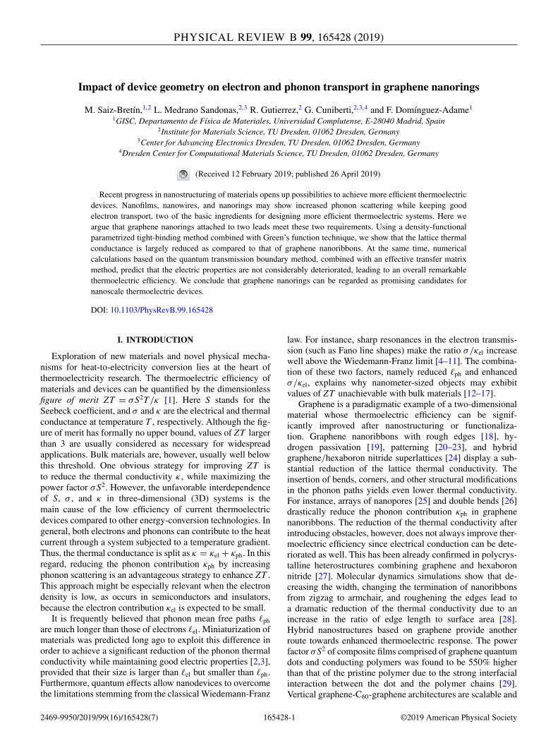
FIG. 2. Phonon transmission τph as function of the phonon fre-quency [(a), (c), and (e)] and phonon thermal conductance κph asa function of temperature [(b), (d), and (f)] for symmetrical (top),asymmetrical (middle), and orthogonal (bottom) configurations. Forall the rings w0 = 1.23 nm and w is indicated in the legend. Grayshadowed curves represent the results for a graphene ribbon ofwidth w0.
do so, we keep w0 = 1.23 nm and, for each type of ring,three different arm widths are considered: w = 0.4w0, w =w0, and w = 1.5w0. Note the latter case does not presenta hole.
The phonon transmission coefficient τph(ω) and thephonon thermal conductance κph for a graphene ribbon ofwidth w0 (as reference system) and all the above-mentionedrings are presented in Fig. 2. We observe that there are twoclearly distinguishable regimes in the thermal conductancefor the three configurations. In the case of symmetric rings,the critical temperature separating both regimes is around30–50 K [see Fig. 2(b)]. Above this temperature, the ribbonhas the highest thermal conductance and for the rings itdecreases as the arms becomes narrower. Below that criticaltemperature, the behavior is radically the opposite and all therings show a larger conductance than the graphene ribbon,though. In Fig. 2(a) it can also be seen that the phonontransmission τph decreases for narrower w with the exceptionof the lowest frequencies, where a peak arises for the casew = 0.4w0. Further below, it will be discussed whether ornot phonon interference is responsible for this counterintuitivephenomenon.
Both the asymmetric and orthogonal configurations presenta similar behavior to the symmetric one. However, whilethe asymmetric configuration also shows a critical temper-ature around 30–50 K, the orthogonal one has a lowerone around 10 K. Again, below the critical temperature the
165428-3
M. SAIZ-BRETÍN et al. PHYSICAL REVIEW B 99, 165428 (2019)
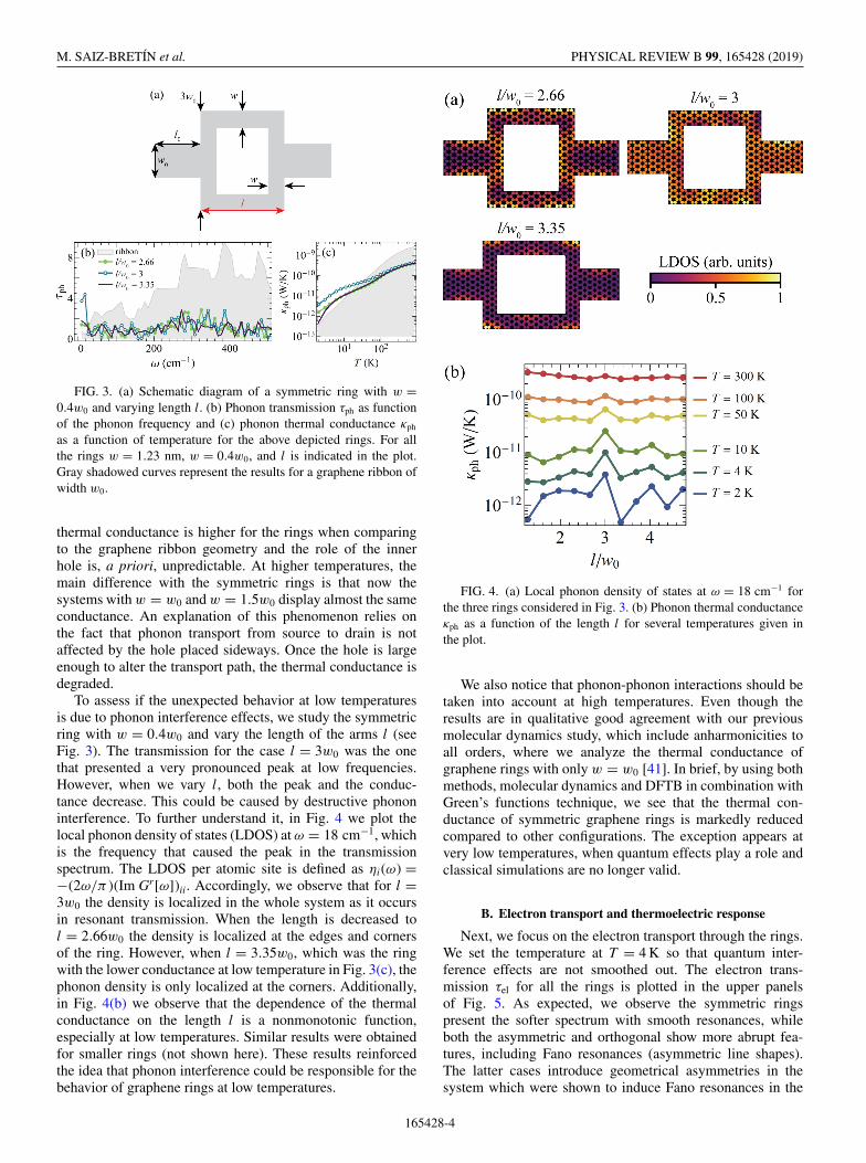
FIG. 3. (a) Schematic diagram of a symmetric ring with w =0.4w0 and varying length l . (b) Phonon transmission τph as functionof the phonon frequency and (c) phonon thermal conductance κph
as a function of temperature for the above depicted rings. For allthe rings w = 1.23 nm, w = 0.4w0, and l is indicated in the plot.Gray shadowed curves represent the results for a graphene ribbon ofwidth w0.
thermal conductance is higher for the rings when comparingto the graphene ribbon geometry and the role of the innerhole is, a priori, unpredictable. At higher temperatures, themain difference with the symmetric rings is that now thesystems with w = w0 and w = 1.5w0 display almost the sameconductance. An explanation of this phenomenon relies onthe fact that phonon transport from source to drain is notaffected by the hole placed sideways. Once the hole is largeenough to alter the transport path, the thermal conductance isdegraded.
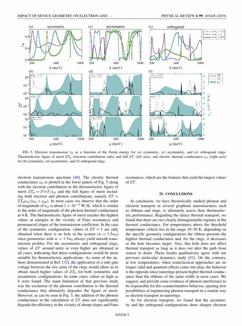
To assess if the unexpected behavior at low temperaturesis due to phonon interference effects, we study the symmetricring with w = 0.4w0 and vary the length of the arms l (seeFig. 3). The transmission for the case l = 3w0 was the onethat presented a very pronounced peak at low frequencies.However, when we vary l , both the peak and the conduc-tance decrease. This could be caused by destructive phononinterference. To further understand it, in Fig. 4 we plot thelocal phonon density of states (LDOS) at ω = 18 cm−1, whichis the frequency that caused the peak in the transmissionspectrum. The LDOS per atomic site is defined as ηi(ω) =−(2ω/π )(Im Gr[ω])ii. Accordingly, we observe that for l =3w0 the density is localized in the whole system as it occursin resonant transmission. When the length is decreased tol = 2.66w0 the density is localized at the edges and cornersof the ring. However, when l = 3.35w0, which was the ringwith the lower conductance at low temperature in Fig. 3(c), thephonon density is only localized at the corners. Additionally,in Fig. 4(b) we observe that the dependence of the thermalconductance on the length l is a nonmonotonic function,especially at low temperatures. Similar results were obtainedfor smaller rings (not shown here). These results reinforcedthe idea that phonon interference could be responsible for thebehavior of graphene rings at low temperatures.
FIG. 4. (a) Local phonon density of states at ω = 18 cm−1 forthe three rings considered in Fig. 3. (b) Phonon thermal conductanceκph as a function of the length l for several temperatures given inthe plot.
We also notice that phonon-phonon interactions should betaken into account at high temperatures. Even though theresults are in qualitative good agreement with our previousmolecular dynamics study, which include anharmonicities toall orders, where we analyze the thermal conductance ofgraphene rings with only w = w0 [41]. In brief, by using bothmethods, molecular dynamics and DFTB in combination withGreen’s functions technique, we see that the thermal con-ductance of symmetric graphene rings is markedly reducedcompared to other configurations. The exception appears atvery low temperatures, when quantum effects play a role andclassical simulations are no longer valid.
B. Electron transport and thermoelectric response
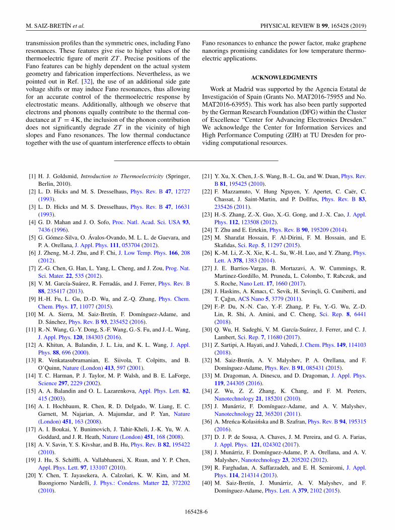
Next, we focus on the electron transport through the rings.We set the temperature at T = 4 K so that quantum inter-ference effects are not smoothed out. The electron trans-mission τel for all the rings is plotted in the upper panelsof Fig. 5. As expected, we observe the symmetric ringspresent the softer spectrum with smooth resonances, whileboth the asymmetric and orthogonal show more abrupt fea-tures, including Fano resonances (asymmetric line shapes).The latter cases introduce geometrical asymmetries in thesystem which were shown to induce Fano resonances in the
165428-4
IMPACT OF DEVICE GEOMETRY ON ELECTRON AND … PHYSICAL REVIEW B 99, 165428 (2019)
FIG. 5. Electron transmission τel as a function of the Fermi energy for (a) symmetric, (c) asymmetric, and (e) orthogonal rings.Thermoelectric figure of merit ZTel (electron contribution only) and full ZT (left axis), and electric thermal conductance κel (right axis)for (b) symmetric, (d) asymmetric, and (f) orthogonal rings.
electron transmission spectrum [40]. The electric thermalconductance κel is plotted in the lower panels of Fig. 5 alongwith the electron contribution to the thermoelectric figure ofmerit ZTel = S2σT/κel and the full figure of merit includ-ing both electron and phonon contributions, namely ZT =ZTelκel/(κel + κph). In most cases we observe that the orderof magnitude of κel is about 1 × 10⁻¹² W/K, which is similarto the order of magnitude of the phonon thermal conductanceat 4 K. The thermoelectric figure of merit reaches the highestvalues at energies in the vicinity of Fano resonances andpronounced slopes of the transmission coefficient. In the caseof the symmetric configuration, values of ZT ≈ 1 are onlyobtained when there is no hole in the system (w = 1.5w0)since geometries with w < 1.5w0 always yield smooth trans-mission profiles. For the asymmetric and orthogonal rings,values of ZT around unity or even higher are obtained inall cases, indicating that these configurations would be moresuitable for thermoelectric applications. As some of the au-thors demonstrated in Ref. [32], the application of a side-gatevoltage between the two arms of the rings would allow us toobtain much higher values of ZTel for both symmetric andasymmetric configurations. In some cases values as high as8 were found. The main limitation of that previous studywas the exclusion of the phonon contribution to the thermalconductance that ultimately degrades the figure of merit.However, as can be seen in Fig. 5, the addition of the phononconductance in the calculation of ZT does not significantlydegrade the efficiency in the vicinity of abrupt slopes and Fano
resonances, which are the features that yield the largest valuesof ZT .
IV. CONCLUSIONS
In conclusion, we have theoretically studied phonon andelectron transport in several graphene nanostructures suchas ribbons and rings, to ultimately assess their thermoelec-tric performance. Regarding the lattice thermal transport, wefound that there are two clearly distinguishable regimes in thethermal conductance. For temperatures above the thresholdtemperature (which lies in the range 10–50 K, depending onthe specific geometry configuration) the ribbon presents thehighest thermal conductance and, for the rings, it decreasesas the hole becomes larger. Also, this hole does not affectthermal transport as long as it does not alter the path fromsource to drain. These results qualitatively agree with ourprevious molecular dynamics study [41]. On the contrary,at low temperatures, when semiclassical approaches are nolonger valid and quantum effects come into play, the behavioris the opposite since nanorings present higher thermal conduc-tance than the ribbons of the same width in most cases. Wesuggest, and provide some evidence of phonon interference tobe responsible for this counterintuitive behavior, opening newpossibilities of engineering phonon transport in a similar wayas electron transport in nanorings.
As for electron transport, we found that the asymmet-ric and the orthogonal configurations show sharper electron
165428-5
M. SAIZ-BRETÍN et al. PHYSICAL REVIEW B 99, 165428 (2019)
transmission profiles than the symmetric ones, including Fanoresonances. These features give rise to higher values of thethermoelectric figure of merit ZT . Precise positions of theFano features can be highly dependent on the actual systemgeometry and fabrication imperfections. Nevertheless, as wepointed out in Ref. [32], the use of an additional side gatevoltage shifts or may induce Fano resonances, thus allowingfor an accurate control of the thermoelectric response byelectrostatic means. Additionally, although we observe thatelectrons and phonons equally contribute to the thermal con-ductance at T = 4 K, the inclusion of the phonon contributiondoes not significantly degrade ZT in the vicinity of highslopes and Fano resonances. The low thermal conductancetogether with the use of quantum interference effects to obtain
Fano resonances to enhance the power factor, make graphenenanorings promising candidates for low temperature thermo-electric applications.
ACKNOWLEDGMENTS
Work at Madrid was supported by the Agencia Estatal deInvestigación of Spain (Grants No. MAT2016-75955 and No.MAT2016-63955). This work has also been partly supportedby the German Research Foundation (DFG) within the Clusterof Excellence “Center for Advancing Electronics Dresden.”We acknowledge the Center for Information Services andHigh Performance Computing (ZIH) at TU Dresden for pro-viding computational resources.
[1] H. J. Goldsmid, Introduction to Thermoelectricity (Springer,Berlin, 2010).
[2] L. D. Hicks and M. S. Dresselhaus, Phys. Rev. B 47, 12727(1993).
[3] L. D. Hicks and M. S. Dresselhaus, Phys. Rev. B 47, 16631(1993).
[4] G. D. Mahan and J. O. Sofo, Proc. Natl. Acad. Sci. USA 93,7436 (1996).
[5] G. Gómez-Silva, O. Ávalos-Ovando, M. L. L. de Guevara, andP. A. Orellana, J. Appl. Phys. 111, 053704 (2012).
[6] J. Zheng, M.-J. Zhu, and F. Chi, J. Low Temp. Phys. 166, 208(2012).
[7] Z.-G. Chen, G. Han, L. Yang, L. Cheng, and J. Zou, Prog. Nat.Sci. Mater. 22, 535 (2012).
[8] V. M. García-Suárez, R. Ferradás, and J. Ferrer, Phys. Rev. B88, 235417 (2013).
[9] H.-H. Fu, L. Gu, D.-D. Wu, and Z.-Q. Zhang, Phys. Chem.Chem. Phys. 17, 11077 (2015).
[10] M. A. Sierra, M. Saiz-Bretín, F. Domínguez-Adame, andD. Sánchez, Phys. Rev. B 93, 235452 (2016).
[11] R.-N. Wang, G.-Y. Dong, S.-F. Wang, G.-S. Fu, and J.-L. Wang,J. Appl. Phys. 120, 184303 (2016).
[12] A. Khitun, A. Balandin, J. L. Liu, and K. L. Wang, J. Appl.Phys. 88, 696 (2000).
[13] R. Venkatasubramanian, E. Siivola, T. Colpitts, and B.O’Quinn, Nature (London) 413, 597 (2001).
[14] T. C. Harman, P. J. Taylor, M. P. Walsh, and B. E. LaForge,Science 297, 2229 (2002).
[15] A. A. Balandin and O. L. Lazarenkova, Appl. Phys. Lett. 82,415 (2003).
[16] A. I. Hochbaum, R. Chen, R. D. Delgado, W. Liang, E. C.Garnett, M. Najarian, A. Majumdar, and P. Yan, Nature(London) 451, 163 (2008).
[17] A. I. Boukai, Y. Bunimovich, J. Tahir-Kheli, J.-K. Yu, W. A.Goddard, and J. R. Heath, Nature (London) 451, 168 (2008).
[18] A. V. Savin, Y. S. Kivshar, and B. Hu, Phys. Rev. B 82, 195422(2010).
[19] J. Hu, S. Schiffli, A. Vallabhaneni, X. Ruan, and Y. P. Chen,Appl. Phys. Lett. 97, 133107 (2010).
[20] Y. Chen, T. Jayasekera, A. Calzolari, K. W. Kim, and M.Buongiorno Nardelli, J. Phys.: Condens. Matter 22, 372202(2010).
[21] Y. Xu, X. Chen, J.-S. Wang, B.-L. Gu, and W. Duan, Phys. Rev.B 81, 195425 (2010).
[22] F. Mazzamuto, V. Hung Nguyen, Y. Apertet, C. Caër, C.Chassat, J. Saint-Martin, and P. Dollfus, Phys. Rev. B 83,235426 (2011).
[23] H.-S. Zhang, Z.-X. Guo, X.-G. Gong, and J.-X. Cao, J. Appl.Phys. 112, 123508 (2012).
[24] T. Zhu and E. Ertekin, Phys. Rev. B 90, 195209 (2014).[25] M. Sharafat Hossain, F. Al-Dirini, F. M. Hossain, and E.
Skafidas, Sci. Rep. 5, 11297 (2015).[26] K.-M. Li, Z.-X. Xie, K.-L. Su, W.-H. Luo, and Y. Zhang, Phys.
Lett. A 378, 1383 (2014).[27] J. E. Barrios-Vargas, B. Mortazavi, A. W. Cummings, R.
Martinez-Gordillo, M. Pruneda, L. Colombo, T. Rabczuk, andS. Roche, Nano Lett. 17, 1660 (2017).
[28] J. Haskins, A. Kınacı, C. Sevik, H. Sevinçli, G. Cuniberti, andT. Çagın, ACS Nano 5, 3779 (2011).
[29] F.-P. Du, N.-N. Cao, Y.-F. Zhang, P. Fu, Y.-G. Wu, Z.-D.Lin, R. Shi, A. Amini, and C. Cheng, Sci. Rep. 8, 6441(2018).
[30] Q. Wu, H. Sadeghi, V. M. García-Suárez, J. Ferrer, and C. J.Lambert, Sci. Rep. 7, 11680 (2017).
[31] Z. Sartipi, A. Hayati, and J. Vahedi, J. Chem. Phys. 149, 114103(2018).
[32] M. Saiz-Bretín, A. V. Malyshev, P. A. Orellana, and F.Domínguez-Adame, Phys. Rev. B 91, 085431 (2015).
[33] M. Dragoman, A. Dinescu, and D. Dragoman, J. Appl. Phys.119, 244305 (2016).
[34] Z. Wu, Z. Z. Zhang, K. Chang, and F. M. Peeters,Nanotechnology 21, 185201 (2010).
[35] J. Munárriz, F. Domínguez-Adame, and A. V. Malyshev,Nanotechnology 22, 365201 (2011).
[36] A. Mrenca-Kolasinska and B. Szafran, Phys. Rev. B 94, 195315(2016).
[37] D. J. P. de Sousa, A. Chaves, J. M. Pereira, and G. A. Farias,J. Appl. Phys. 121, 024302 (2017).
[38] J. Munárriz, F. Domínguez-Adame, P. A. Orellana, and A. V.Malyshev, Nanotechnology 23, 205202 (2012).
[39] R. Farghadan, A. Saffarzadeh, and E. H. Semiromi, J. Appl.Phys. 114, 214314 (2013).
[40] M. Saiz-Bretín, J. Munárriz, A. V. Malyshev, and F.Domínguez-Adame, Phys. Lett. A 379, 2102 (2015).
165428-6
IMPACT OF DEVICE GEOMETRY ON ELECTRON AND … PHYSICAL REVIEW B 99, 165428 (2019)
[41] M. Saiz-Bretín, A. V. Malyshev, F. Domínguez-Adame, D.Quigley, and R. A. Römer, Carbon 127, 64 (2018).
[42] B. Aradi, B. Hourahine, and T. Frauenheim, J. Phys. Chem. A111, 5678 (2007).
[43] C. S. Lent and D. J. Kirkner, J. Appl. Phys. 67, 6353 (1990).[44] D. Z.-Y. Ting, E. T. Yu, and T. C. McGill, Phys. Rev. B 45, 3583
(1992).[45] J. Schelter, D. Bohr, and B. Trauzettel, Phys. Rev. B 81, 195441
(2010).[46] H. Sevinçli, C. Sevik, T. Çagin, and G. Cuniberti, Sci. Rep. 3,
1228 (2013).[47] L. Medrano Sandonas, H. Sevinçli, R. Gutierrez, and G.
Cuniberti, Adv. Sci. 5, 1700365 (2018).
[48] T. Niehaus, M. Elstner, T. Frauenheim, and S. Suhai, J. Mol.Struc. 541, 185 (2001).
[49] I. Milosevic, N. Kepcija, E. Dobardzic, M. Damnjanovic, M.Mohr, J. Maultzsch, and C. Thomsen, Int. J. Mod. Phys. B 24,655 (2010).
[50] L. Medrano Sandonas, D. Teich, R. Gutierrez, T. Lorenz, A.Pecchia, G. Seifert, and G. Cuniberti, J. Phys. Chem. C 120,18841 (2016).
[51] L. Medrano Sandonas, R. Gutierrez, A. Pecchia, G. Seifert,and G. Cuniberti, Phys. Chem. Chem. Phys. 19, 1487(2017).
[52] J. Munárriz, Modelling of Plasmonic and Graphene Nanode-vices (Springer, Berlin, 2014).
165428-7


![PHYSICAL REVIEW B99 Evolution of the propagation vector ......2Si 2,arethe multipolar ordered phases in NpO 2 [2–4] and CeB 6 [5,8–13]. The cage compound Ce 3Pd 20Si 6, which is](https://img.pdfslide.us/doc/110x75/6119a3f677ae5a635618e75d/physical-review-b99-evolution-of-the-propagation-vector-2si-2arethe-multipolar.jpg)


![PHYSICAL REVIEW B99, 115101 (2019) · computationally very demanding especially if applied self-consistently [8]. Within the generalized Kohn-Sham (gKS) scheme [9] (i.e., with nonmultiplicative](https://img.pdfslide.us/doc/110x75/606afa47e124be08cd1f6baa/physical-review-b99-115101-2019-computationally-very-demanding-especially-if.jpg)


![PHYSICAL REVIEW B99, 085312 (2019) · 2019. 7. 18. · three- and two-dimensional semiconductor systems [16–23]. A distinction of the light impact ionization reported in the present](https://img.pdfslide.us/doc/110x75/60ec637def2a3c210c78cb65/physical-review-b99-085312-2019-2019-7-18-three-and-two-dimensional-semiconductor.jpg)
![PHYSICAL REVIEW B99, 205145 (2019)scalettar.physics.ucdavis.edu/publications/PhysRevB.99...trons [11]. Thus the extended Hubbard model (EHH), which includes electron-electron interactions](https://img.pdfslide.us/doc/110x75/6065df3e1a74020b0e651578/physical-review-b99-205145-2019-trons-11-thus-the-extended-hubbard-model.jpg)