Embed Size (px)
Citation preview

IEEE TRANSACTIONS ON ELECTRON DEVICES, VOL. 59, NO. 5, MAY 2012 1353
Physical Insight Toward Heat Transport andan Improved Electrothermal ModelingFramework for FinFET Architectures
Mayank Shrivastava, Member, IEEE, Manish Agrawal, Sunny Mahajan, Harald Gossner, Senior Member, IEEE,Thomas Schulz, Dinesh Kumar Sharma, Senior Member, IEEE, and V. Ramgopal Rao, Senior Member, IEEE
Abstract—We report on the thermal failure of fin-shaped field-effect transistor (FinFET) devices under the normal operatingcondition. Pre- and postfailure characteristics are investigated. Adetailed physical insight on the lattice heating and heat flux in a3-D front end of the line and complex back end of line—of a logiccircuit network—is given for bulk/silicon-on-insulator (SOI) Fin-FET and extremely thin SOI devices using 3-D TCAD. Moreover,the self-heating behavior of both the planar and nonplanar devicesis compared. Even bulk FinFET shows critical self-heating. Lay-out, device, and technology design guidelines (based on complex3-D TCAD) are given for a robust on-chip thermal management.Finally, an improved framework is proposed for an accurateelectrothermal modeling of various FinFET device architecturesby taking into account all major heat flux paths.
Index Terms—BEOL reliability, electrothermal modeling, ESD,extremely thin silicon on insulator (SOI) (ETSOI), fin-shapedfield-effect transistor (FET) (FinFET), thermal fail.
I. INTRODUCTION
W ITH THE downscaling of technology down to the20-nm node, planar devices have shown degraded
switching characteristics [1]. This has motivated researchersto come up with a number of nonconventional planar andnonplanar CMOS devices, such as tunnel field-effect transistors(FETs), fin-shaped FETs (FinFETs), nanowire FETs, impactionization MOS, and extremely thin silicon-on-insulator (SOI)(ETSOI) FETs, as technology options for sub-22-nm node gatelengths [2]–[4]. One such device which shows tremendouspotential to scaling, while maintaining CMOS compatibility, isFinFET. FinFET is a nonplanar device with a thin fin betweensource and drain forming the channel. The thin fin is surroundedby the gate on the top three sides, with thickness and heightof the fin defining the effective channel width. Among the twoimportant kinds of FinFETs—SOI and bulk—both the devices
Manuscript received December 7, 2011; revised February 5, 2012; acceptedFebruary 9, 2012. Date of publication March 8, 2012; date of current versionApril 25, 2012. This work was supported by Infineon Technologies AG,Munich, Germany (currently, Intel Mobile Communications Gmbh). Thereview of this paper was arranged by Editor R. Venkatasubramanian.
M. Shrivastava, H. Gossner, and T. Schulz are with Intel Mobile Com-munications Gmbh, 85622 Munich, Germany (e-mail: [email protected]).
M. Agrawal was with the Indian Institute of Technology Bombay, Mumbai400 076, India. He is now with Intel Corporation, Bangalore 560 017, India.
S. Mahajan, D. K. Sharma, and V. R. Rao are with the Indian Institute ofTechnology Bombay, Mumbai 400 076, India (e-mail: [email protected]).
Color versions of one or more of the figures in this paper are available onlineat http://ieeexplore.ieee.org.
Digital Object Identifier 10.1109/TED.2012.2188296
show almost the same on-to-off current ratio [5]–[7]. However,the differences appear due to factors such as junction leakage,parasitic capacitances, etc. In SOI FinFETs, it becomes easierto avoid latchup and achieve desired performance, because ofthe isolation provided by the buried oxide (BOX) [7], [8].Alternatively, extremely thin body SOI (ETSOI) FETs weredemonstrated as an option for sub-22-nm gate lengths, withadvantages such as lower 3-D parasitics, ease of incorporatingstrain effects, flexibility in width selection, and suppressedrandom dopant fluctuation [9], [10].
The electrical characteristics of these devices are well under-stood; however, thermal behavior still needs a detailed study.These devices are expected to suffer from heavy self-heating,as nanoscale dimensions in the devices cause a high thermalresistance between heat source and sink, causing poor ther-mal coupling. It is due to this self-heating that the saturationcurrents in SOI devices get reduced by almost 10%–15% andthe maximum allowable frequency gets limited [11]. The in-crease in overall temperature due to the device’s self-heatingdegrades many other important parameters including chip’slifetime [12], [13]. The basic phenomenon behind the self-heating is attributed to electron phonon interaction occurring inthe high-electric-field region near the drain-to-channel junction.The detailed physics behind heat generation and its conductionwithin semiconductors is explained elsewhere [14], [15].
So far, there have been several studies on possible heat flowpaths in FinFETs [16]–[21]. Few of them claim interconnectto be the prime heat flow path, while others assume that mostof the heat should leave through the substrate of the chip,i.e., silicon (Si) body. As per [17], maximum heat dissipatesout through the BOX, whereas [18]–[20] establish the factthat most of the heat indeed gets away from active regionthrough interconnect metals. In [19], authors have comparedmetal/polygate FinFETs for their impact on the self-heatingbehavior and have found metal gates to give better thermalperformance, thus supporting the fact that significant part of theheat flows through gate contacts and, hence, through intercon-nects. These investigations [16]–[21] were, however, based oncertain assumptions on thermal boundary condition, which arenot always realistic.
So far, different electrothermal models for the same havebeen proposed [22]–[24]. The models in [23] and [24] consistof lumped resistances for the entire sections of the deviceeven though the heat flux paths are 3-D in nature. FinFET-like devices necessitate modeling of the sections with finer
0018-9383/$31.00 © 2012 IEEE

1354 IEEE TRANSACTIONS ON ELECTRON DEVICES, VOL. 59, NO. 5, MAY 2012
granularity in order to achieve a better accuracy while includingthe 3-D nature of heat flux, which is missing in the literature. Inaddition to this, the boundary conditions in these models [22]–[24] assume an isothermal surface next to the electrical contactswithout including the BEOL topology and assuming that mostof the heat leaves through BOX. Also, the additional rise intemperature due to hot ambience caused by neighboring devicesswitching simultaneously has been ignored in previous studies.Moreover, often, adiabatic boundaries are assumed for all othersurfaces, which is a debatable issue. Such boundary conditionsrule out any heat flux via the bottom silicon substrate. A prac-tical definition of thermal boundary condition is still missing inthe literature. In another study, a new device structure was pro-posed in order to relieve self-heating in FinFET devices [21].This proposal was based on the thermal boundary conditionsdiscussed in [22]–[24], with the limitations discussed earlier.
Extending the previous work on heat flux in realistic BEOLof ETSOI and SOI FinFETs [25], this paper emphasizes our in-vestigations on bulk FinFETs and guidelines for 3-D lumped el-ement modeling. Moreover, this paper performs the following:
1) establishes practical thermal boundary conditions;2) gives a proper understanding of the heat transport by
taking into account realistic BEOL structures;3) provides design guidelines taking BEOL details into ac-
count and their impact on thermal management;4) includes additional temperature rise due to hot ambience
caused by devices switching simultaneously in the neigh-borhood;
5) describes the impact of various FinFET device architec-tures on thermal management by taking into account allmajor heat flux paths into account.
This paper is arranged as follows. Experimental results andTCAD calibrations are presented in Sections II and III, respec-tively, while physical insight into the thermal behavior and heattransport in ETSOI and SOI/bulk FinFET devices is given inSection IV. Moreover, we have provided useful FEOL/BEOLdesign guidelines for sub-22-nm node device options inSection IV, by taking into account complete BEOL/FEOLdetails in our investigations. A new framework is proposed foran accurate electrothermal modeling of FinFET-like architec-tures in Section V, which takes all major heat flux paths intoaccount extracted from 3-D TCAD simulation. In Section VI,we have demonstrated the performance of various trigate andtall-fin FinFET architectures using our proposed model. Finally,Section VII concludes this paper.
II. DEVICE FABRICATION AND EXPERIMENTAL RESULTS
Undoped trigate FinFET devices were fabricated with a metalmidgap TiN gate and SiON dielectric (EOT = 1.9 nm). Allfins are processed with a target width of 15 nm and length of70 nm and are of 60-nm height.
A. Experiments
Fig. 1 shows IDS–VDS characteristics of the fabricated Fin-FET devices. While stressing beyond VDS = 1 V, it can beobserved that the device suffers from high impact ionization at
Fig. 1. Measured ID–VD characteristics of a FinFET device. Mitigatedimpact ionization at higher bias conditions shows the presence of significantself-heating.
lower gate bias under which the drain current is extremely lowcompared to its ON current (ION). However, almost negligibleimpact ionization at higher gate bias (i.e., higher drain current)was observed. It is evident that the observed impact ionizationcurrent is due to a high lateral electric field (under low verticalelectric field) at smaller gate bias and higher drain bias. Therecan be two distinct physical arguments for the observed behav-ior at high drain and gate bias, i.e., high electric field and currentdensity.
1) The lateral electric field is lowered near the drain underhigh gate bias, which eventually mitigates impact ioniza-tion at drive current.
2) Under high drive current and high lateral electric field,the device gives rise to a significantly higher latticetemperature, which eventually degrades the generation ofexcess carriers from impact ionization [26], [27].
TCAD simulations prove that self-heating is the dominatingeffect. The device significantly suffers from self-heating evenunder low operating condition (∼2 × VDD). It is worth men-tioning that the device failed after three to four measurementswhen it was stressed under VDS = VGS = 2 V (∼2 × VDD).Fig. 2 compares the leakage behavior of the virgin device andthe failed device. It is evident from Fig. 2 that the devicesuffered a thermal failure, which further motivates the require-ment of modeling electrothermal behavior in various FinFETarchitectures.
B. Discussion
In order to validate our arguments and motivation, Fig. 3shows a typical failure picture of a FinFET device stressed for100 ns under a high current (= 6 mA/µm) and a high electricfield (VDRAIN = 3 V), which can easily lead to thermal failureby giving rise to a lattice temperature (TMAX)1 above 1000 K[28]. Moreover, our TCAD simulations predict a temperaturerise of 400 K–500 K under nominal operating conditions (i.e.,VDD = 1 V and ION ∼ 0.5 mA/µm), when stressed for 1 ms.Based on these observations, one can easily predict the thermal
1TMAX ∝∫
J.Edt, where J is the current density, E is the electric field,and dt is the stress time.

SHRIVASTAVA et al.: INSIGHT TOWARD HEAT TRANSPORT AND MODELING FRAMEWORK 1355
Fig. 2. (a) and (b) Post- and prefailure currents. The figures show significantlyhigh leakage current after three measurements. Postfailure characteristics showa very low resistance path from drain to gate and from drain to source, whichin conjunction with self-heating behavior (Fig. 1) validates an early thermalfailure.
Fig. 3. SEM (failure analysis) picture of a FinFET device, which shows atypical thermal fail of the device under ESD-like stress condition.
behavior of FinFETs or similar nanoscale devices operating atan ON current ∼1 mA/µm or higher [29].
III. MODEL CALIBRATION AND TCAD FRAMEWORK
A well-calibrated 3-D device simulation deck was used forthis work where the source/drain and channel doping profilesof realized devices were extracted from Monte Carlo implant(atomistic) simulations [30]. Fig. 4 shows the calibration ofTCAD model parameters for drift–diffusion transport consid-ering quantum corrections at the oxide–silicon channel inter-
Fig. 4. Calibration of TCAD models for 3-D drift–diffusion transport (consid-ering quantum corrections) with experimental data. Note that the left and righty-axes are on linear and log scales, respectively.
Fig. 5. (a) Two-stage driving inverter with full BEOL definition. (b) Temper-ature distribution up to seven metal layers which shows the impact of boundaryconditions.
face, which is carefully matched with the experimental data.The channel in FinFET is on the sidewall of the fin thatlies on a (110) plane, if the device is fabricated on a waferhaving orientation (100). Due to the dissimilar effective massvalues along the various axes, hole mobility in FinFET getsenhanced, and electron mobility gets degraded as compared toconventional planar devices with (100) surface orientation [31].Sidewall roughness, stress, and strain also affect the mobility.Since the default model parameters of the device simulatorare for (100) plane, the mobility model parameters have beenmodified for (110) plane. The values of the model parameterswere then extrapolated to 22-nm LG devices as described in[32]. The contact resistivity value chosen for all simulations is2.4 × 10−8 Ω · cm2.
In order to fully capture the heat flux through variousinterconnect lines and interlayer dielectric (ILD) regions, atwo-stage Inverter-driving-inverter with full BEOL definitionis realized for TCAD simulations, which is shown in Fig. 5.Layout rules for 22-nm length scale were taken from predictive

1356 IEEE TRANSACTIONS ON ELECTRON DEVICES, VOL. 59, NO. 5, MAY 2012
TABLE IDIMENSIONAL/LAYOUT AND THERMAL PARAMETERS
TAKEN FROM [30], [33], AND [34]
technology model [33]. The simulation approach used in thiswork is to extract quasi-static temperature (i.e., the worst casetemperature), which should be the cumulative rise in peaktemperature after 1000 s of pulses, and is discussed in ourwork elsewhere [20]. Thermal properties of various regionsare calibrated as per their exact dimensions and region-specificmaterial used in a typical CMOS process flow. Table I showsvarious layout/dimensional and calibrated thermal parametersused for TCAD simulations. The same is used later for derivinga modified electrothermal model and related framework.
IV. PHYSICAL INSIGHT AND DESIGN GUIDELINES
Figs. 5(b) and 6 show the temperature distribution acrossBEOL (i.e., along the interconnect metals) and FEOL (i.e.,in the active regions) of a two-stage inverter designed usingFinFET devices. Fig. 6 shows that hot spot is located near thedrain-to-channel junction. Channel current under the influenceof high lateral electric field at drain-to-channel junction leadsto strong heat dissipation (due to the phonon generation),which eventually gives rise to a significant lattice temperature.Moreover, Fig. 7 shows that maximum contribution of heatflux is through metal interconnect instead of Si body unlikethe theories presented in [17]. This was observed for SOIFinFET, ETSOI devices, as well as for bulk FinFETs too. Thisbehavior is attributed to the following: 1) high thermal resis-
Fig. 6. (a) Heat flux per unit area from various heat sinkers (or thermalcontacts). (b) Temperature distribution across the interconnect metals and active(Si) region along different planes. The figures show the following: 1) NMOShas a higher temperature rise as compared to PMOS; 2) devices close toI/O pads have lower heating as compared to others, which is due to bettercooling conditions; and 3) maximum heat flux is through interconnect metalsas compared to BOX and ILD layers.
tance of the silicon substrate compared to metal interconnects;2) significantly lower thermal conductivity of thin silicon fins;and 3) substrate/Si-body topology in bulk FinFETs. A simplecalculation shows that the thermal resistance of a Si body

SHRIVASTAVA et al.: INSIGHT TOWARD HEAT TRANSPORT AND MODELING FRAMEWORK 1357
Fig. 7. Percentage of heat flux coming out from various parts of the inves-tigated logic network designed using (a) SOI FinFET, (b) bulk FinFET, and(c) ETSOI devices, respectively. The figures show that most of the thermalenergy flows through interconnect metals, whereas the back side of the chip(Si body) has a negligible contribution on the overall heat flux coming out ofthe chip.
was 15× higher compared to that of a metal interconnect.Note that the thermal resistances (for a unit cross sectionarea) of 100-nm-thick BOX, 1-µm-long metal interconnect, and250-µm-thick Si body are 71 nK · m2/W, 2.6 nK · m2/W, and1.7 µK · m2/W, respectively. Such a high thermal resistancecontributed by Si body leads to most of the heat to sink intothe overlying back-end metallization instead of the siliconbody. Moreover, substrate topology in bulk FinFETs (a narrowinactive fin surrounded by STI, which is in between hot spot andlarge Si body) does not allow dumping all heat in the Si body ina similar fashion as it does for planar bulk MOS devices. Notethat NMOS devices have a higher temperature rise as comparedto PMOS, which is due to a relatively higher drive current ofNMOS device.
A. Impact of Device Scaling
Fig. 8 shows the impact of technology scaling over the self-heating behavior. As a rule of thumb [34], if a FinFET devicewith a fin width (WFIN) of 15 nm and a channel length (LG)of 25 nm scales down to LG = 16 nm, its fin width should alsoscale down from 15 down to 8 nm, in order to keep the leakageunchanged. This will eventually scale down the fin heightfrom 45 down to 24 nm, to keep the aspect ratio unchanged.Considering the trends shown in Fig. 8 and the aforementionedrule of thumb, one can get an indication that technology scalingshould not affect the thermal performance significantly if finwidth and fin height are scaled simultaneously with channellength scaling. Moreover, Fig. 9 shows self-heating effects inthe logic network designed using ETSOI device. It is evidentfrom Figs. 8 and 9 that ETSOI devices suffer less from self-heating compared to FinFET device.
It is worth mentioning that the rise in lattice temperaturedepends on the following: 1) volume of power source (activeregion); 2) volume of heat sink in the surrounding area; and3) thermal boundary conditions in the exteriors which definethe quasi-static temperature rise. Relaxed lattice temperature
Fig. 8. Impact of scaling gate length and fin height on the self-heatingbehavior. The figure shows the following: 1) ETSOI device has a smallertemperature rise as compared to FinFET device, and 2) fin height scaling inFinFET device (similar to active area scaling of ETSOI) and gate length scalingcan counterbalance the self-heating effect.
Fig. 9. Self-heating in ETSOI devices. It shows relaxed self-heating in ETSOIdevice, which is due to lower volume of power source while keeping the BEOLsame.
in ETSOI device can be attributed to a smaller power densitywithin a given volume of active Si region in ETSOI devicecompared to the same in FinFET device, while keeping theBEOL definition identical for both the devices.
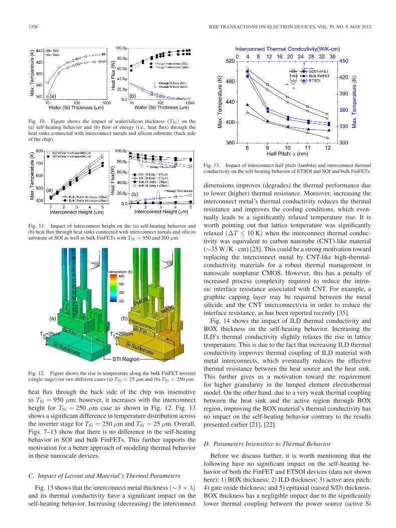
B. Impact of Wafer Thickness and Interconnect Height
In order to validate our argument about the significant risein lattice temperature due to a 15× higher thermal resistanceof Si body compared to that of metal interconnect, the impactof Si-body thickness and interconnect height is investigated inthis section. Fig. 10(a) shows that, when the substrate thicknesswas greatly reduced, the rise in overall temperature relaxessignificantly, which is attributed to an increased flow of ther-mal energy through heat sink connected with the Si body asshown in Fig. 10(b). Moreover, Fig. 11 shows that, when theinterconnect height is increased, the overall temperature risessignificantly for a thicker substrate (TSi = 950 m) as well asfor a thinner substrate (TSi = 250 µm). On the other hand,
1358 IEEE TRANSACTIONS ON ELECTRON DEVICES, VOL. 59, NO. 5, MAY 2012
Fig. 10. Figure shows the impact of wafer/silicon thickness (TSi) on the(a) self-heating behavior and (b) flow of energy (i.e., heat flux) through theheat sinks connected with interconnect metals and silicon substrate (back sideof the chip).
Fig. 11. Impact of interconnect height on the (a) self-heating behavior and(b) heat flux through heat sinks connected with interconnect metals and siliconsubstrate of SOI as well as bulk FinFETs with TSi = 950 and 200 µm.
Fig. 12. Figure shows the rise in temperature along the bulk FinFET inverter(single stage) for two different cases (a) TSi = 25 µm and (b) TSi = 250 µm.
heat flux through the back side of the chip was insensitiveto TSi = 950 µm; however, it increases with the interconnectheight for TSi = 250 µm case as shown in Fig. 12. Fig. 13shows a significant difference in temperature distribution acrossthe inverter stage for TSi = 250 µm and TSi = 25 µm. Overall,Figs. 7–13 show that there is no difference in the self-heatingbehavior in SOI and bulk FinFETs. This further supports themotivation for a better approach of modeling thermal behaviorin these nanoscale devices.
C. Impact of Layout and Material’s Thermal Parameters
Fig. 13 shows that the interconnect metal thickness (∼3 × λ)and its thermal conductivity have a significant impact on theself-heating behavior. Increasing (decreasing) the interconnect
Fig. 13. Impact of interconnect half pitch (lambda) and interconnect thermalconductivity on the self-heating behavior of ETSOI and SOI and bulk FinFETs.
dimensions improves (degrades) the thermal performance dueto lower (higher) thermal resistance. Moreover, increasing theinterconnect metal’s thermal conductivity reduces the thermalresistance and improves the cooling conditions, which even-tually leads to a significantly relaxed temperature rise. It isworth pointing out that lattice temperature was significantlyrelaxed (∆T ≤ 10 K) when the interconnect thermal conduc-tivity was equivalent to carbon nanotube (CNT)-like material(∼35 W/K · cm) [25]. This could be a strong motivation towardreplacing the interconnect metal by CNT-like high-thermal-conductivity materials for a robust thermal management innanoscale nonplanar CMOS. However, this has a penalty ofincreased process complexity required to reduce the intrin-sic interface resistance associated with CNT. For example, agraphite capping layer may be required between the metalsilicide and the CNT interconnect/via in order to reduce theinterface resistance, as has been reported recently [35].
Fig. 14 shows the impact of ILD thermal conductivity andBOX thickness on the self-heating behavior. Increasing theILD’s thermal conductivity slightly relaxes the rise in latticetemperature. This is due to the fact that increasing ILD thermalconductivity improves thermal coupling of ILD material withmetal interconnects, which eventually reduces the effectivethermal resistance between the heat source and the heat sink.This further gives us a motivation toward the requirementfor higher granularity in the lumped element electrothermalmodel. On the other hand, due to a very weak thermal couplingbetween the heat sink and the active region through BOXregion, improving the BOX material’s thermal conductivity hasno impact on the self-heating behavior contrary to the resultspresented earlier [21], [22].
D. Parameters Insensitive to Thermal Behavior
Before we discuss further, it is worth mentioning that thefollowing have no significant impact on the self-heating be-havior of both the FinFET and ETSOI devices (data not shownhere): 1) BOX thickness; 2) ILD thickness; 3) active area pitch;4) gate oxide thickness; and 5) epitaxial (raised S/D) thickness.BOX thickness has a negligible impact due to the significantlylower thermal coupling between the power source (active Si

SHRIVASTAVA et al.: INSIGHT TOWARD HEAT TRANSPORT AND MODELING FRAMEWORK 1359
Fig. 14. Impact of BOX’s and ILD’s thermal conductivities on the self-heatingbehavior of ETSOI and SOI and bulk FinFETs.
fin) and the heat sink connected at the back side of Si body viaBOX. Gate oxide has almost a negligible impact on self-heatingeffects because of its extremely low thermal resistance (due toits physical thickness) compared to that of metal interconnects.
V. MODIFIED MODELING FRAMEWORK
Based on our understanding of heat flux paths, interregionthermal coupling, and various key contributors toward the self-heating behavior, a thermal resistance network is derived bythe following: 1) discretizing the device into a finer meshof resistances along the dominant heat flux paths within thedevice; 2) considering the 3-D nature of device and associatedheat flux moving out of the device; and 3) thermal couplingbetween adjacent regions.
A. Building Blocks
The device is divided into sections where each section of thedevice (fin, channel, gate, source, drain, spacer, and intercon-nects) is further subdivided into smaller elements (i.e., “Block,”“Ch,” and “Pad”). Fig. 15(a) shows the block element, whichmodels the nonchannel regions of the fin, the gate, and spacers.R1, R3, and R5 account for the heat flux path via the BOXand the Si body (bulk Si). R2 and R4 model the path alongthe length of the element. The other Rxy resistances model thelateral heat conduction paths and serve to couple the adjacentregions via the ILD. Moreover, Fig. 15(b) shows the channelelement (Ch) used for modeling the heat conduction through achannel region. Finally, Fig. 15(c) shows contact pad element(Pad), which models the gate, source, and drain contact pads.R0 models the heat flux path from fin to pad. Ri accounts for theheat flux path to interconnects through the via, and Rb modelsthe heat flux path via BOX and the Si body (bulk Si). R1 andR2 resistances model lateral heat conduction paths for couplingof pads to adjacent fins. In addition to the heat flux pathsmodeled by the block element, this model adds Rox for theadditional heat flux path through the gate oxide. The parametersof the nominal FinFET device are presented in Table I. Variousthermal resistances for the basic building blocks of the modelmentioned earlier are derived in the Appendix. A complete 3-D
Fig. 15. Overall approach for the thermal-resistance-network-based modelfor electrothermal simulations. (a) Block element of the model (Block).(b) Channel element (Ch). (c) Pad element (Pad).
Fig. 16. Complete 3-D representation of the thermal model used for variousFinFET architectures.
representation of the thermal model used for various FinFETarchitectures is shown in Fig. 16.
B. Heat Source and Boundary Conditions
Joule heating (near the drain end of the channel) and clas-sical heat diffusion are considered for computing the totalrise in lattice temperature using the relation ∇(λ∇T ) = −η,where λ is the thermal conductivity of various heat flux paths(given in Table I); heat generated (η) is approximated fromthe product of the current density (J) and the electric field(E). For this study, J and E values where extracted from3-D TCAD simulations. Isothermal boundary conditions withan ambient temperature = 300 K (outside of the chip) isconsidered.
C. Validation
Fig. 17 shows that the model derived from the proposedframework gives an excellent fit with the predictions made from

1360 IEEE TRANSACTIONS ON ELECTRON DEVICES, VOL. 59, NO. 5, MAY 2012
Fig. 17. Figure shows matching of model predictions with TCAD data with-out any fitting parameter. This validates the accuracy of the proposed modelingframework.
TABLE IIINFLUENCE OF KEY DEVICE/TECHNOLOGY/MATERIAL PARAMETERS
OVER SELF HEATING BEHAVIOR, DERIVED FOR TWO DIFFERENT CASES:(A) WHEN CHANGE IN ELECTRICAL CONDITIONS WERE CONSIDERED
AND (B) SOLE IMPACT OF THERMAL BOUNDARY CONDITIONS
TCAD (and summarized in Table II) without including anyfitting parameter.
VI. TRIGATE VERSUS TALL-FIN FINFETS
This section investigates the self-heating behavior of someother FinFET device architectures using our derived model andcompares the same with TCAD-derived predictions.
Fig. 18 compares three different device configurations, i.e.,(a) trigate FinFET [Aspect Ratio (AR) = 1 with WFIN =30 nm, (b) tall-fin (AR = 7) FinFET with fin volume con-served, and (c) tall-fin (AR = 7) FinFET with fin-to-gate in-terface area conserved. Configuration “b” keeps the thermalresistance along the length of the fin the same as in the trigateFinFET—configuration “a.” This allows us to investigate theimpact of the other conduction path, i.e., from the channel to the
Fig. 18. Self-heating behavior predicted by the proposed model for trigate andtall-fin architectures on bulk and SOI substrates.
gate contact (via the gate oxide + gate metal). Configuration“c” keeps the thermal resistance from the channel to the gatecontact the same as in the trigate FinFET and allows us tostudy the effect of the other conduction paths, i.e., along thelength of the channel. Overall, Fig. 18 shows that the trigatearchitecture has a better thermal performance in comparison toboth the tall-fin configurations, which is attributed to increasedSi volume underneath the active fin region or hot spot. Thishelps in dumping most of the heat into the Si body in a similarfashion as it does for planar bulk MOS devices. It is worthpointing out that this behavior is in a good agreement with thepredictions made from TCAD.
VII. CONCLUSION
We have studied the thermal failure of FinFET devices undernominal operating conditions. Our work clearly establishes thefact that, due to a huge thermal resistance contributed by theSi body and the 3-D topology of Si substrate in bulk FinFETstructures, there is no difference in the thermal behavior of bulkand SOI FinFET devices. Trigate FinFET devices and planarETSOI devices were found to have better thermal performancecompared to various tall-fin FinFET (bulk/SOI) architectures.CNT-like high-thermal-conductivity materials for interconnectswere found to be the key requirement to resolve the thermal is-sues in these nanoscale CMOS technologies. The importance ofthermal boundary conditions is discussed. Our results demon-strate that, in order to build a 3-D thermal resistance networkfor FinFET-like devices, proper knowledge of various heat fluxpaths and thermal coupling between the various regions orblocks must be considered. Based on this knowledge, a newframework is proposed in this paper for accurate electrothermalmodeling of nanoscale FinFET devices. This modified modeltakes into account the 3-D nature of the device and includesthe possible heat flux paths and necessary thermal couplingbetween the different regions/blocks of the device. It was foundthat scaling of all the layout/technology parameters does nothave the same impact on the self-heating behavior, i.e., only afew parameters in BEOL have the maximum impact. Based onour investigations, a design guideline is extracted and summa-rized for robust thermal management.

SHRIVASTAVA et al.: INSIGHT TOWARD HEAT TRANSPORT AND MODELING FRAMEWORK 1361
APPENDIX
Various thermal resistances for the basic building blocks ofthe model mentioned in Section V are derived in this section.
Drain/Source, Fin (Blocks):
R1 =HBOXeff4×kBOX
+ 1αeff
Wfin × Lfinelement(SOI)
R1 =HBOXeffbulk
4×kBOX+ 1
αeff
Wfin × Lfinelement(Bulk)
R2 =Lfinelement
2 × kfinSi × Wfin × Hfin
R4 =Lfinelement
2 × kfinSi × Wfin × Hfin
R3 =HBOXeff2×kBOX
+ 1αeff
Wfin × Lfinelement(SOI)
R3 =HBOXeffbulk
2×kBOX+ 1
αeff
Wfin × Lfinelement(Bulk)
R5 =HBOXeff4×kBOX
+ 1αeff
Wfin × Lfinelement(SOI)
R5 =HBOXeffbulk
4×kBOX+ 1
αeff
Wfin × Lfinelement(Bulk)
R61 =Wpad − Wfin
8 × kILD × Lfinelement × Hfin
R63 =Wpad − Wfin
4 × kILD × Lfinelement × Hfin
R65 =Wpad − Wfin
8 × kILD × Lfinelement × Hfin
R71 =Wpad − Wfin
8 × kILD × Lfinelement × Hfin
R73 =Wpad − Wfin
4 × kILD × Lfinelement × Hfin
R75 =Wpad − Wfin
8 × kILD × Lfinelement × Hfin
HBOXeff = HBOX +HBottomSi × kBOX
kBottomSi
HBOXeffbulk =(HBOX + HBottomSi) × kBOX
kBottomSi
Lelement =Lfin
Nfin.
Drain/Source/Gate Contacts (Pad):
R1 =Wpad
2 × knonchannelSi × HSD × Lpad
R2 =Wpad
2 × knonchannelSi × HSD × Lpad
RO =(Lpad − Lcontact) × 2. 3025 × log
(Wcontact
Wfin
)
2 × knonchannelSi × HSD × (Wcontact − Wfin)
Ri =Hcontact
kcontact × Lcontact × Wcontact
Rb =HBOXeff
kBOX × Wpad × Lpad+
1αeff × Wpad × Lpad
(SOI)
Rb =1
kBOX×(Wpad−Wfin)×LpadHBOXeff
+ kBOX×(Wpad−Wfin)×LpadHBOXeffbulk
+αeff
Wpad × Lpad(Bulk).
Channel (Block and Ch):
Rox =tox
2 × kox × Hfin × Lchannel + kox × Wfin × Lchannel.
ACKNOWLEDGMENT
The authors would like to thank the MicroelectronicsGroup, Indian Institute of Technology Bombay, Mumbai, India;W. Molzer; and Intel Mobile Communications Gmbh, Munich,Germany, for various interesting discussions on this topic.
REFERENCES
[1] B. Parvais, A. Mercha, N. Collaert, R. Rooyackers, I. Ferain,M. Jurczak, V. Subramanian, A. De Keersgieter, T. Chiarella, C. Kerner,L. Witters, S. Biesemans, and T. Hoffman, “The device architec-ture dilemma for CMOS technologies: Opportunities and challenges ofFinFET over planar MOSFET,” in Proc. Symp. VLSI Technol., Syst. Appl.,2009, pp. 80–81.
[2] H. Kawasaki, M. Khater, M. Guillorn, N. Fuller, J. Chang,S. Kanakasabapathy, L. Chang, R. Muralidhar, K. Babich, Q. Yang,J. Ott, D. Klaus, E. Kratschmer, E. Sikorski, R. Miller, R. Viswanathan,Y. Zhang, J. Silverman, Q. Ouyang, A. Yagishita, M. Takayanagi,W. Haensch, and K. Ishimaru, “Demonstration of highly scaled FinFETSRAM cells with high-κ/metal gate and investigation of characteristicvariability for the 32 nm node and beyond,” in IEDM Tech. Dig., 2008,pp. 1–4.
[3] Y. Jiang, T. Y. Liow, N. Singh, L. H. Tan, G. Q. Lo, D. Chan, andD. L. Kwong, “Nanowire FETs for low power CMOS applications fea-turing novel gate-all-around single metal FUSI gates with dual Φm andV T tune-ability,” in IEDM Tech. Dig., 2008, pp. 1–4.
[4] J.-P. Colinge, FinFETs and Other Multi-Gate Transistors. New York:Springer-Verlag, 2008.
[5] C. R. Manoj, N. Meenakshi, V. Dhanya, and V. R. Rao, “Device design& optimization considerations for bulk FinFETs,” IEEE Trans. ElectronDevices, vol. 55, no. 2, pp. 609–615, Feb. 2008.
[6] T.-S. Park, H. J. Cho, J. D. Choe, S. Y. Han, D. Park, K. Kim, E. Yoon, andJ.-H. Lee, “Characteristics of the full CMOS SRAM cell using body-tiedTG MOSFETs (bulk FinFETs),” IEEE Trans. Electron Devices, vol. 53,no. 3, pp. 481–487, Mar. 2006.
[7] K. Okano, T. Izumida, H. Kawasaki, A. Kaneko, A. Yagishita,T. Kanemura, M. Kondo, S. Ito, N. Aoki, K. Miyano, T. Ono,K. Yahashi, K. Iwade, T. Kubota, T. Matsushita, I. Mizushima, S. Inaba,K. Ishimaru, K. Suguro, K. Eguchi, Y. Tsunashima, and H. Ishiuchi,“Process integration technology and device characteristics of CMOS Fin-FET on bulk silicon substrate with sub-10 nm fin width and 20 nm gatelength,” in IEDM Tech. Dig., 2008, pp. 721–724.
[8] L. T. Su, J. E. Chung, D. A. Antoniadis, K. E. Goodson, and M. I. Flik,“Measurement and modeling of self-heating in SOI nMOSFETs,” IEEETrans. Electron Devices, vol. 41, no. 1, pp. 69–75, Jan. 1994.
[9] O. Weber, O. Faynot, F. Andrieu, C. Buj-Dufournet, F. Allain, P. Scheib-lin, J. Foucher, N. Daval, D. Lafond, L. Tosti, L. Brevard, O. Rozeau,C. Fenouillet-Beranger, M. Marin, F. Boeuf, D. Delprat, K. Bourdelle,B.-Y. Nguyen, and S. Deleonibus, “High immunity to threshold voltagevariability in undoped ultra-thin FDSOI MOSFETs and its physical un-derstanding,” in IEDM Tech. Dig., 2008, pp. 1–4.
[10] M. Shrivastava, B. Verma, M. S. Baghini, C. Russ, D. K. Sharma,H. Gossner, and V. R. Rao, “Benchmarking the device performance atsub 22 nm node Technologies using an SoC framework,” in IEDM Tech.Dig., 2009, pp. 1–4.
[11] K. A. Franch and R. L. Jenkins, “Impact of self-heating on digital SOIand strained-silicon CMOS circuits,” in Proc. IEEE Int. SOI Conf., 2003,pp. 161–163.
[12] S. K. Cheng and P. Manos, “Effects of operating temperature on electricalparameters in an analog process,” IEEE Circuits Devices Mag., vol. 5,no. 4, pp. 31–38, Jul. 1989.
[13] Y.-K. Choi, D. Ha, E. Snow, J. Bokor, and T.-J. King, “Reliability studyof CMOS FinFETs,” in IEDM Tech. Dig., 2003, pp. 7.6.1–7.6.4.

1362 IEEE TRANSACTIONS ON ELECTRON DEVICES, VOL. 59, NO. 5, MAY 2012
[14] K. E. Goodson and P. Eric, “Thermal phenomena in nanoscale transis-tors,” in Proc. Conf. Thermal Thermo Mech. Phenom. Electron. Syst.,2004, pp. 1–7.
[15] A. D. McConnell and K. E. Goodson, “Thermal conduction in siliconmicro- and nano structures,” in Proc. Annu. Rev. Heat Transf., 2005,pp. 129–168.
[16] M. Berger and Z. Chai, “Estimation of heat transfer in SOI-MOSFET,”IEEE Trans. Electron Devices, vol. 38, no. 4, pp. 871–875, Apr. 1991.
[17] S. P. Sinha, M. Pelella, C. Tretz, and C. Riccobene, “Assessing circuitlevel impact of self-heating in 0.13 µm SOI CMOS,” in Proc. SOI Conf.,2001, pp. 101–102.
[18] F. Yu and M.-C. Cheng, “Heat flow in SOI current mirrors,” in Proc.Semicond. Device Res. Symp., 2003, pp. 392–393.
[19] R. V. Joshi, C. T. Chuang, K. Keunwoo, J. Y. Murthy, and E. J. K. Nowak,“Self-consistent and efficient electro thermal analysis for poly/metal gateFinFETs,” in IEDM Tech. Dig., 2006, pp. 1–4.
[20] M. Shrivastava, M. S. Baghini, D. K. Sharma, and V. R. Rao, “A novelbottom spacer FinFET structure for improved short-channel, power-delay,and thermal performance,” IEEE Trans. Electron Devices, vol. 57, no. 6,pp. 1287–1294, Jun. 2010.
[21] Z. X. Zhang, Q. Lin, M. Zhu, and C. L. Lin, “A new structure of SOIMOSFET for reducing self-heating effects,” Ceram. Int., vol. 30, no. 7,pp. 1289–1293, 2004.
[22] S. Kolluri, K. Endo, E. Suzuki, and K. Banerjee, “Modeling and analysisof self-heating in FinFET devices for improved circuit and EOS/ESDperformance,” in IEDM Tech. Dig., 2007, pp. 177–180.
[23] B. Swahn and S. Hassoun, “Electro-thermal analysis of multi-fin devices,”IEEE Trans. Very Large Scale Integr. (VLSI) Syst., vol. 16, no. 7, pp. 816–829, Jul. 2008.
[24] E. Pop, R. Dutton, and K. Goodson, “Thermal analysis of ultra-thin bodydevice scaling,” in IEDM Tech. Dig., 2003, pp. 36.6.1–36.6.4.
[25] M. Shrivastava, M. Agrawal, J. Aghassi, H. Gossner, W. Molzer,T. Schulz, and V. R. Rao, “On the thermal failure in nanoscale devices:Insight towards heat transport including critical BEOL and design guide-lines for robust thermal management & EOS/ESD reliability,” in Proc.Int. Reliab. Phys. Symp., 2011, pp. 3F.3.1–3F.3.5.
[26] S. Reggiani, M. Rudan, E. Gnani, and G. Baccarani, “Investigation aboutthe high-temperature impact-ionization coefficient in silicon,” in Proc.34th ESSDERC, 2004, pp. 245–248.
[27] M. Valdinoci, D. Ventura, M. C. Vecchi, M. Rudan, G. Baccarani, F. Illien,A. Stricker, and L. Zullino, “Impact-ionization in silicon at large operatingtemperature,” in Proc. SISPAD, 1999, pp. 27–30.
[28] H. Gossner, C. Russ, F. Siegelin, J. Schneider, K. Schruefer, T. Schulz,C. Duvvury, C. R. Cleavelin, and W. Xiong, “Unique ESD failure mecha-nism in a MuGFET technology,” in IEDM Tech. Dig., 2006, pp. 1–4.
[29] C.-Y. Chang, T.-L. Lee, C. Wann, L.-S. Lai, H.-M. Chen, C.-C. Yeh,C.-S. Chang, C.-C. Ho, J.-C. Sheu, T.-M. Kwok, F. Yuan, S.-M. Yu,C.-F. Hu, J.-J. Shen, Y.-H. Liu, C.-P. Chen, S.-C. Chen, L.-S. Chen,L. Chen, Y.-H. Chiu, C.-Y. Fu, M.-J. Huang, Y.-L. Huang, S.-T. Hung,J.-J. Liaw, H.-C. Lin, H.-H. Lin, L.-T. S. Lin, S.-S. Lin, Y.-J. Mii,E. Ou-Yang, M.-F. Shieh, C.-C. Su, S.-P. Tai, H.-J. Tao, M.-H. Tsai,K.-T. Tseng, K.-W. Wang, S.-B. Wang, J. J. Xu, F.-K. Yang, S.-T. Yang,and C.-N. Yeh, “A 25-nm gate-length FinFET transistor module for 32 nmnode,” in IEDM Tech. Dig., 2009, pp. 1–4.
[30] Version 2010.03 Synopsys TCAD suite.[31] T. Rudenko, N. Collaert, S. De Gendt, V. Kilchytska, M. Jurczak, and
D. Flandre, “Effective mobility in FinFET structures with HfO2 and SiONgate dielectrics and TaN gate electrode,” Microelectron. Eng., vol. 80,pp. 386–389, Jun. 2005.
[32] R. Granzner, V. M. Polyakov, F. Schwierz, M. Kittler, R. J. Luyken,W. Rösner, and M. Städele, “Simulation of nanoscale MOSFETs usingmodified drift–diffusion and hydrodynamic models and comparison withMonte Carlo results,” Microelectron. Eng., vol. 83, no. 2, pp. 241–246,Feb. 2006.
[33] Predictive Technology Models. [Online]. Available: www.eas.asu.edu/~ptm
[34] M. Shrivastava, R. Mehta, S. Gupta, N. Agrawal, M. S. Baghini,D. K. Sharma, T. Schulz, K. von Arnim, W. Molzer, H. Gossner, andV. R. Rao, “Toward system on chip (SoC) development using FinFETtechnology: Challenges, solutions, process co-development & optimiza-tion guidelines,” IEEE Trans. Electron Devices, vol. 58, no. 6, pp. 1597–1607, Jun. 2011.
[35] Y. Chai, A. Hazeghi, K. Takei, H.-Y. Chen, P. C. H. Chan, A. Javey, andH.-S. P. Wong, “Low-resistance electrical contact to carbon nanotubeswith graphitic interfacial layer,” IEEE Trans. Electron Devices, vol. 59,no. 1, pp. 12–19, Jan. 2012.
Mayank Shrivastava (S’09–M’10) received theB.S. degree in engineering from Rajiv Gandhi Tech-nical University, Bhopal, India, in 2006 and the Ph.D.degree from the Indian Institute of Technology (IIT)Bombay, Mumbai, India, in 2010.
From April 2008 to October 2008 and, again,from May 2010 to July 2010, he was a VisitingResearch Scholar with Infineon Technologies AG,Munich, Germany. From 2010 to 2011, he was withInfineon Technologies, East Fishkill, NY, and withIntel Mobile Communications, Hopewell Junction,
NY, as a Senior Electrostatic Discharge (ESD) Engineer for InternationalSemiconductor Development Alliance. He is currently with Intel MobileCommunications Gmbh, Munich. He has over 30 publications in internationaljournals/conferences and is the holder of 12 patents issued or pending in thefield of ESD protection, drain-extended MOS devices, fin-shaped field-effecttransistors (FETs), tunnel FETs, electrothermal modeling, RF power amplifiers,and nonvolatile memory. He is a Reviewer of the Japanese Journal of AppliedPhysics and Microelectronics Reliability.
Dr. Shrivastava was a recipient of the India TR35 Award for the year 2010(Young Innovator Award from MIT Technology Review 35); the 2008 BestResearch Paper Award in circuit design category from Intel Corporation AsiaAcademic Forum; the 2010 Industrial Impact Award from IIT Bombay; thebiography publication by the International Biographical Center, Cambridge,U.K., in the 2000 Outstanding Intellectuals of the 21st Century in 2010; theExcellence in Thesis Work for his Ph.D. thesis from IIT Bombay in 2010; andthe Infineon Fellowship from 2008 to 2010. He has served as a subcommitteemember of 2012 EOS/ESD Symposium and as a Reviewer for various inter-national journals, which include the IEEE TRANSACTIONS ON ELECTRON
DEVICES, IEEE ELECTRON DEVICE LETTERS, and IEEE TRANSACTIONS
ON DEVICE AND MATERIALS RELIABILITY.
Manish Agrawal, photograph and biography not available at the time ofpublication.
Sunny Mahajan, photograph and biography not available at the time ofpublication.
Harald Gossner (M’06–SM’11) received theDipl.Phys. degree in physics from Ludwig-Maximilians-Universität, Munich, Germany, in 1990and the Ph.D. degree in electrical engineering fromthe Universität der Bundeswehr, Munich, in 1995.
Recently, he has joined Intel Mobile Commu-nications Gmbh, Munich, where he is currently aSenior Principal Engineer for Electrostatic Discharge(ESD), overseeing the development of robust mobilesystems there. For 15 years, he was with Siemensand Infineon Technologies where he worked on the
development of ESD protection concepts for bipolar, BiCMOS, and CMOStechnologies. He has authored and coauthored more than 80 technical papersand one book in the field of ESD and device physics. He is the holder of 30patents on the same topic.
Dr. Gossner is a member of ESDA and EDS. He was a recipient of theBest Paper Award of EOSESD 2005. Regularly, he is lecturing tutorials atESREF, IRPS, and EOSESD symposia. He has served in technical programcommittees of IEDM, EOSESD Symposium, and International ESD Workshop.He currently belongs to the management teams of IEW and EOSESD. In 2006,he became a Cofounder of the Industry Council on ESD Target Levels, where hehas been cochairing this committee of 50 leading electronics and IC companies.

SHRIVASTAVA et al.: INSIGHT TOWARD HEAT TRANSPORT AND MODELING FRAMEWORK 1363
Thomas Schulz received the Dipl.-Ing. and Dr.-Ing. degrees in electrical engineering from the Ruhr-University Bochum, Bochum, Germany, in 1997 and2001, respectively.
In 2000, he joined the Corporate Research NanoDevice Group, Infineon Technologies AG, Munich,Germany, where he worked on novel device con-cepts. From 2004 to 2006, he was a Member ofthe Technical Staff, Infineon Technologies NorthAmerica, International Sematech/ATDF, Austin, TX,where he worked on multigate-FET project. In 2006,
he joined IMEC, Leuven, Belgium, where he worked on device developmentprojects as a Senior Staff Engineer of Infineon Technologies, Leuven. SinceFebruary 1, 2011, he has been with Intel Mobile Communications Gmbh,Munich, Germany. He authored or coauthored over 40 conference and journalpublications and has been a holder of over 40 patents in the field of devicedesign with others pending.
Mr. Schulz is currently a member of the European ITRS PIDS and ERDworking groups. Over the last 10 years, he contributed to several national andinternational research projects like NANOCMOS, PULLNANO, and UTTER-MOST. He serves as a Reviewer of the IEEE TRANSACTIONS ON ELECTRON
DEVICES and IEEE ELECTRON DEVICE LETTERS.
Dinesh Kumar Sharma (M’98–SM’01) receivedthe Ph.D. degree from the University of Bombay,Mumbai, India.
He was with the Solid-State Electronics Group,TIFR, during 1971–1991, except for 1976–1978,when he was a Visiting Scientist with LETI, Greno-ble, France, and 1985–1987, when he was withthe Microelectronics Center, Research Triangle Park,NC. Since 1991, he has been with the EE Depart-ment, Indian Institute of Technology Bombay, Mum-bai, where he is currently a Professor and the Head
of the department. Over the last 35 years, he has worked in the areas of MOSdevice modeling, VLSI technology development, VLSI digital system design,mixed-signal design, and RF design. He has also contributed to research inprocess and device simulation, electrothermal modeling, and characterizationof MOS devices. He has published more than 50 papers in reputed journalsand conferences on these subjects. He maintains close contact with the micro-electronics industry in India. He has designed several ICs for the industry andhas conducted training courses for them in the areas of VLSI technology anddesign. His current interests include RF and mixed-signal VLSIs, asynchronousdesign, and the effect of technology and device scaling on design architecturesand tools. Over the last few years, he has also been working on manpowertraining in the areas of microelectronics and VLSI design in India. He hasserved on several committees within the government, which are trying toimprove the general level of training in this area. He has also collaborated withthe industry and coauthored a widely quoted report with Dr. F. C. Kohli of TCSon this subject. He serves on the editorial board of Pramana, the journal ofphysics from the Indian Academy of Science.
Dr. Sharma is a Fellow of the Institution of Electronics and Telecommuni-cation Engineers (IETE). He was a recipient of the Bapu Sitaram Award of theIETE for Excellence in Research and Development in electronics in 2001.
V. Ramgopal Rao (M’98–SM’02) received theM.Tech. degree from the Indian Institute of Tech-nology Bombay (IIT Bombay), Mumbai, India, in1991 and the Dr.Ing. degree from the Universität derBundeswehr, Munich, Germany, in 1997.
From 1997 to 1998 and, again, in 2001, he wasa Visiting Scholar with the Department of ElectricalEngineering, University of California, Los Angeles.He currently holds the Institute Chair Professor posi-tion with the Department of Electrical Engineering,IIT Bombay, where he is the Chief Investigator for
the Centre of Excellence in Nanoelectronics. He has over 300 publicationsin the area of electron devices and nanoelectronics in refereed internationaljournals and conference proceedings and is the holder of 16 patents issued orpending.
Dr. Rao was a recipient of the coveted Shanti Swarup Bhatnagar Prize inEngineering Sciences awarded by the Honorable Prime Minister, Governmentof India, in 2005 for his work on electron devices. He was also a recipientof the 2004 Swarnajayanti Fellowship Award from the Department of Scienceand Technology, the 2007 IBM Faculty Award, the 2008 Materials ResearchSociety of India Annual Prize, and the 2009 TechnoMentor Award from theIndian Semiconductor Association. He is an Editor for the IEEE TRANS-ACTIONS ON ELECTRON DEVICES in the CMOS devices and technologyarea and serves on the editorial boards of various other international journals.He is a Fellow of the Indian National Academy of Engineering, the IndianAcademy of Sciences, and the National Academy of Sciences in India. He is aDistinguished Lecturer, IEEE Electron Devices Society, and has served on theprogram/organizing committees of a large number of international conferencesin the area of electron devices. He was a Chairman, IEEE AP/ED BombayChapter, during 2002–2003 and currently serves on the executive committeeof the IEEE Bombay Section in addition to being the Vice Chair, IEEE Asia-Pacific Regions/Chapters Subcommittee.