Embed Size (px)
Citation preview

IEEE JOURNAL OF SELECTED TOPICS IN QUANTUM ELECTRONICS, VOL. 12, NO. 4, JULY/AUGUST 2006 669
Photonics for Switching and RoutingDavid T. Neilson, Senior Member, IEEE
(Invited Paper)
Abstract—The ongoing growth of data traffic from existing andnew applications poses a challenge to the packet-switched networkinfrastructure. High-capacity transport can be achieved in suchnetworks by using dense wavelength-division-multiplexed systems,and reconfigurable optical add–drop multiplexers allow the opti-cal layer to provision wavelength-based circuits between routingnodes. However, construction of the high-capacity packet routersprovides significant scaling issues due to complexity, interconnect,and thermal limits. In this paper we will not seek to cover allaspects of optical packet switching and routing but outline someof the challenges facing the construction of such future routersand describe the role photonics can have in overcoming some ofthese issues. We will discuss how photonics’ primary role will beto provide interconnection between racks of electronic routing el-ements and describe how fast wavelength switching can provide ahigh-capacity distributed switch fabric that will allow these packetrouters to scale to higher capacities. The fast wavelength switch-ing can be seen as the packet analog of wavelength-based circuitswitching of today’s transparent optical networks.
Index Terms—Optical interconnections, optical switches, packetswitches, wavelength switching.
I. INTRODUCTION
COMUNICATION networks continue to radically trans-form the way in which we mange and use information.
They exhibit rapid growth in capacity driven by a broad rangeof new applications. Specifically, the Internet or packet-basednetwork shows approximate doubling (1.7×–2.5×) of trafficeach year [1], [2]. This trend has continued steadily despitemany changes in the dominant applications and services pro-vided by the network. Similarly, its growth rate has continuedwith significant broadening of the user base and transformationfrom the original government and academic sectors to the com-mercial sector. It has also had significant geographical spreadfrom the first world to become a global network. With the in-creased deployment of broadband access and new applicationsincluding voice over Internet protocol (VoIP) and Internet proto-col television (IPTV), it is reasonable to assume that this growthrate will continue for the foreseeable future [2]. Since the datatraffic on the Internet now exceeds the voice traffic in conven-tional networks, it is now the driving mechanism for growth oflocal, regional, and global communication networks. With evo-lution toward converged networks, the distinction between voicenetworks and data networks is disappearing and private line cir-cuits can be emulated with virtual private networks (VPN). Thismeans that for the network of the future we can consider it to becomposed solely of a packet-switching infrastructure.
Manuscript received December 15, 2005; revised April 21, 2006.The author is with Bell Laboratories, Lucent Technologies, Holmdel, NJ
07733 USA (e-mail: [email protected]).Digital Object Identifier 10.1109/JSTQE.2006.876315
Fig. 1. Current-router-to-network interface (left) where routers are connectedtogether using an optical network consisting of SONET/SDH TDM-ADM net-work elements connected by physical-optical transport layer. Future router tonetwork (right) interface where routers are connected by using packet over theDWDM optical layer with add and drop provided by ROADMs.
To understand the limitations of the current architectures andsystems, let us first consider how they are organized. A sim-ple architecture for a packet-switched network consists of ge-ographically diverse packet routers interconnected by a high-capacity optical network. Today, this optical network employstime-domain multiplexed (TDM) systems such as synchronousoptical network (SONET) and synchronous digital hierarchy(SDH) for provisioning circuits between the routers as illus-trated in Fig. 1. The packet routers maximize the utilization ofthese fixed circuits via statistical multiplexing.
However, the ongoing rapid growth of data traffic on thenetworks poses a challenge both to the transport and to theswitching infrastructure of such a network, since both mustscale rapidly to larger capacities without dramatic increasein size and cost. Dense wavelength-division multiplexing(DWDM) in conjunction with increasing line rates continues toallow the transport capacity to grow gracefully with multiterabitper second per fiber transport systems available today. The useof optical transparency and reconfigurable optical add–dropmultiplexers (ROADMs) [3]–[5] illustrated in Fig. 1 allowsthe provisioning of physical circuits at the optical layer. Thispermits packet transport directly over optical layer circuitsand eliminates or at least reduces the need for high-capacitySONET/SDH TDM network elements. Because of the option touse the optical layer to provision circuits, scaling of these TDMswitches does not pose a bottleneck for network growth [6].
A rising concern, however, is that the packet routers willsoon not be able to support the increasing volumes of traffic atreasonable costs. This may necessitate changes in architectureat the router or network level and possibly also in the hardwaretechnologies that are used to build them.
Today, packet routers are key to enabling the functionality ofthe Internet by forwarding of the packets towards their destina-tion using packet header information and route lookup tables.They also ensure high utilization of the links in the network by
1077-260X/$20.00 © 2006 IEEE

670 IEEE JOURNAL OF SELECTED TOPICS IN QUANTUM ELECTRONICS, VOL. 12, NO. 4, JULY/AUGUST 2006
Fig. 2. Growth in router capacity per rack over time based on year of intro-duction. Including data points from [7] and [8]. Line shows 2× every 18 months(increase of 1.56×/year), which extrapolated, gives 100 Tb/s by 2012.
providing statistical multiplexing. Historically, their capacityhas been doubling every 18 months since the mid-1980s [7], [8]as shown in Fig. 2. The difference between the Internet(2× /year) and router growth (2× /1.5 year) can be attributedto an increase in the number of routers in the network whichis at least partially associated with the growth of the physicalextent and number of the networks connected. This growthrate, if it continues, predicts the need for routers with around100 Tb/s capacity by 2012 and announcements of systems withpotential scalability to these capacities have been made [9].
The voice to data transition of the networks has an additionalimpact for the development of future routers. As the switchingcapacity moves from the TDM switches of the transport layerto the packet layer, the packet routers, with capacities >1 Tb/s,are now supplanting TDM circuit switches as the highest ca-pacity switching systems in the network. Previously, they havebeen able to reusing existing technologies developed for high-capacity TDM systems such as SONET/SDH. Routers must nowbe constructed as the first systems to use new technologies andapproaches for line interface cards, backplane technologies, andswitch fabrics. This transition is occurring at a time in which thescaling of current electronic packet routers or even traditionalTDM circuit switches to sizes larger than 1 Tb/s encountersseveral important challenges.
In this paper, we will discuss what are the challenges for scal-ing to next generation routers. We will discuss the advantagesand limitations of photonic devices and the role they might playin alleviating these challenges. We will consider the role of op-tical interconnects both as a backplane within a rack and as arack-to-rack interconnect. We will describe the role that dis-tributed switching over an optical interconnect for rack-to-rackapplications might play. We will describe what are some of thechallenges for using photonics for implementing router switchfabrics, which can meet the needs of 100-Tb/s routers. In thispaper, we will not seek to cover all aspects of optical packetswitching and routing that have been reported in the literature;specifically excluded is the role of photonics for header pro-cessing and buffering which, if implemented in photonics, willnecessarily be preceded by the use of photonic interconnect andswitching functions.
Besides these challenges associated with the physical switch-ing and infrastructure, there are challenges associated with the
global scheduling of large routers [7], [9]–[13], which does notscale linearly and may result in greatly increased complexityor reduced throughput for the router. A detailed discussion ofthese alternate architectures is beyond the scope of this paper,but the general problem is that the scheduler complexity scalesas the cube of the number of ports it schedules. Thus, eliminatingthe central scheduler without degrading the router performancebecomes a possible goal. We note that optical approaches [7]described here are compatible with these architectural changesand have also been demonstrated [10].
II. CHALLENGES FOR NEXT-GENERATION ROUTERS
The primary challenges for next-generation routers are asso-ciated with power dissipation density and the resulting intercon-nection distances.
To explain the limitations, we will consider the structure ofrouters, which consist of three major components shown inFig. 3. There are line cards (LCs), handling ingress and egress,which connect to the rest of the network via optical-to-electronic(O–E) and electronic-to-optical (E–O) interfaces, which supporta variety of line rates and protocols. The LCs also read thepacket headers and decide where to send a packet next usingforwarding tables and have the ingress and egress buffers. Thereis then a central crossbar switch, which is used to interconnectthe LCs. Finally, there is a scheduler which may be centralizedor partially distributed on the LCs, which attempts to maximizethe throughput by considering the routing requests from eachLC for each of the packets.
Of the challenges to scaling existing packet routers to largersizes, we will first discuss power and heat dissipation, whichlimits the maximum power, and therefore, capacity that canbe accommodated in a single rack of equipment. The powerdissipation of routers has grown with capacity as illustrated inFig. 4, with around a 1.4× increase in power dissipation forevery doubling of capacity.
Taken with the doubling of capacity every 18 months, asshown Fig. 2, in this corresponds to 20% (0.8× /year) energyper bit reduction per year. A 20% per year reduction in powerdissipation is what would be expected when router power dis-sipation becomes dominated inter-chip interconnects where thetransmit energy per bit scales proportionately to the minimumfeature size of the silicon [15], [16].
Current routers are already starting to pose a challenge forscaling in a single rack because a terabits per second router to-day has around 5–6 kW [17] of power dissipation per rack and atypical central office being designed to accommodate racks witha <2-kW dissipation [18] with 6 kW possible by increased spac-ing between racks. While higher power densities up to 20 kW perrack are possible, these would require significant reengineeringof the central office infrastructure and therefore cost.
While the capacity of routers at a given power dissipationwill increase with new generations of silicon by 0.8× /year,this will not be sufficient to meet the increasing router capac-ity demands 1.56× /year illustrated in Fig. 2. This is, therefore,pushing routers to multirack solutions [9], [19]. These multirackrouters have LCs distributed in racks, which are then connected

NEILSON: PHOTONICS FOR SWITCHING AND ROUTING 671
Fig. 3. Schematic of packet router consisting of ingress and egress LCs, a central crossbar switch, and a central scheduler. The egress and ingess LCs are typicallycombined onto a single physical LC. The sceduler and crossbar switches may be redundant to provide robustness.
Fig. 4. Power dissipation of router versus capacity for highest capacity routersat introduction (for routers in Fig. 2). Power dissipation increases by 1.4× for 2×increase in capacity equivalent to a reduction in power dissipation of 0.8×/year.
to a central crossbar switch in another rack. The use of a singlecentralized switch fabric may be limited to a few terabits persecond of capacity, since it is also constrained by the power den-sity and heat dissipations limits of a single rack. Constructionof single-stage high-capacity switches is challenging and a so-lution used today is to build the central switch as a multistageswitch [9], [19] using a Clos [20] network.
An example of a multirack router [19], [21] with 2.5-Tb/s(full-duplex) capacity, a total of 31 kW power dissipation, andfive racks is shown schematically in Fig. 5. Each rack of theLCs contains switch fabrics, which form the first and last stagesof a nonblocking Clos network. Each rack of LCs is connectedto a switch fabric rack to form a three-stage Clos network thatis rearrangably nonblocking. This minimizes the hardware butcreates the complexity of calculating the nonblocking configu-ration. Each LC rack now requires a bidirectional rack-to-rackinterconnect to the central fabric of 320 Gb/s.
These multirack systems result in increased distance betweenthe LCs and the switch fabrics. The distance required betweenracks has to account not only for the physical size of the racksbut the need to distribute the high thermal load racks across acentral office, which requires interconnect distances in the tensto hundreds of meters. These multirack solutions are, therefore,constrained by the interconnections between the chassis andswitch fabrics. These become unwieldy in the electronic domaindue to the wiring density that would be required.
Fig. 5. (a) 2.5-Tb/s router using a multirack configuration and (b) logical.Each of the LC shelves has 32 cards each supporting 10-Gb/s I/O (full-duplex)or 32× 2× 10 Gb/s = 640 Gb/s capacity. They each contain switch fabric witha 2× 320 Gb/s capacity, which forms the first (A) and last stage (A’) of anonblocking Clos network. (b) The 2.5-Tb/s switch shelf contains five switchfabrics (S1 to S5) with 2× 320 Gb/s each (fifth for 1 for N redundancy ofswitch and fiber optics), which form the midstages of the Clos. Each of theswitches in the LC shelves is attached to each of the switches in the switch shelfusing a 80-Gb/s bidirectional link, which is implemented using multimode fiberribbons.
Optical interconnects are already being employed betweenracks in these multirack systems. For example, for the 2.5-Tb/srouter system [19] illustrated in Fig. 5, each of the links betweena LC rack and the switching rack consist of five bundles (four

672 IEEE JOURNAL OF SELECTED TOPICS IN QUANTUM ELECTRONICS, VOL. 12, NO. 4, JULY/AUGUST 2006
active and one spare) each one consisting of an array of 48for a total of 240 multimode fibers (192 active) with VCSEL-based transceiver running at a data rate of 1.8 Gb/s [22] for anaggregate throughput of each fiberoptic array cable of 320 Gb/s.From each bundle, 48 fibers (80 Gb/s) connect to each of themidstage switch fabrics.
Growing the switch fabric further will require multipleswitching racks to be interconnected to build a large multistageswitch fabric that is used to connect the racks of LCs. The Closnetwork [20] is an attractive approach since it allows the useof many small fabrics as a building block for much largerswitches. In principle, very large fabrics can be constructedusing five, seven, or nine stages. However, this results in anonlinear scaling of the number of switch fabrics required withincreasing capacity and an equivalent amount of high-speedinterconnection between stages. For example, extending thefabric of Fig. 5 to a five-stage switch fabric, which wouldsupport 16 racks of LCs or 10 Tb/s of capacity, would require12 racks of switch fabrics and four sets of fiber interconnectseach with a 5-Tb/s bidirectional capacity. The power dissipationof such an approach would be around 170 kW, which is 35%higher power per bit than the 2.5-Tb/s router. Very soon scalingsuch a system would be dominated by the equipment dedicatedto switch racks and interconnects between them. This challengeof building a large central switch fabric is further illustrated byan alternative approach taken for another multirack router sys-tem [9] where a nonblocking central switch is not implemented.The central switch fabric is divided into eight parallel switchingfabrics each consisting of a multistage Benes switching fabric,and buffering is used to mange the additional blocking [23].There is a clear need to have more scalable switch fabrics.
III. ROLE OF PHOTONICS
Photonics is often held out as a potential solution to theseinterconnection problems in electronic systems. However, pho-tonic devices and optical systems have certain advantages anddisadvantages that should be considered carefully to best utilizethem in systems.
First, we will compare some of the fundamental differencesbetween electronics and photonics. Electronics relies upon base-band radio-frequency (RF) communication where as photonicsuses an optical carrier with a frequency (fc) in the hundredsof terahertz as illustrated in Fig. 6. This means that photonicdevices can have an absolute bandwidth (fB), which is largein terms of available spectrum, while being relatively narrowband [fB/(fc + fB)]. For example, an 80-GHz bandwidth for40-Gb/s RZ data is only 0.04% relative bandwidth at 193 THz(1554.4 nm). This has benefits for passive components sincea flat frequency response over the required data bandwidth isrelatively easy to achieve.
The narrow relative bandwidth of a channel also allows formultiple channels to be multiplexed using multiple optical car-riers, giving wavelength division multiplexed (WDM) systems.Amplifiers, such as the erbium-doped fiber amplifier (EDFA),exist in the photonic domain that can provide linear low-noiseperformance over multiple terahertzs. Although these have nar-
Fig. 6. Lower graph shows spectra for 40-Gb/s RZ data: Baseband andon a 193-THz (1554.4 nm) carrier. Upper graph shows loss per unit length(dB/m/GHz) for baseband transmission and (dB/m) optical systems. Losses forbaseband are frequency dependent.
row relative bandwidths of only a few percent [for a C-bandEDFA fB/(fc + fB) = 2%], they can support tens or hundredsof WDM channels. Challenges in optics due to the narrow rel-ative bandwidth arise in functions such as multiplexing fil-ters and laser wavelength control for WDM systems. Here,achieving narrow band filters required to separate signals whilemaintaining absolute frequency stability across temperature ischallenging. Using active temperature stabilization techniquesinvolving heaters or thermoelectric coolers typically solves thetemperature dependence. This adds to the power dissipationof the devices and to their cost and size. It is practical toachieve the stability required by the components for multi-plexing with channel spacing of 25 GHz and greater. Sincethis is frequency range is within the practical modulation rates,there is little need to push to higher channel density for opticalmultiplexing.
Because of the high carrier frequency, the wavelength oflight is short (0.8–1.5 µm) compared to the characteristic wave-length of a baseband RF (>0.1 m). This allows confinementin waveguides of micrometer dimensions using only dielectricmaterials. The absence of metals and their associated induc-tances and capacitances means that very low crosstalk can beachieved. This allows for very dense high-capacity devices andlinks. The absence of metals also permits crossing of waveg-uides or light paths in the same plane. However, the same ef-fect that gives low crosstalk to dense optical links also makeintentional coupling between two transmission lines or waveg-uide difficult. This puts very stringent alignment, a few mi-crometers or less, accuracy requirements on packaging andconnectors.
For electrical interconnects, the distance that a signal cantravel is limited by the distortions due to frequency-dependentloss. The attenuation of a transmission line is given by
Att(dB) = 8.686(
RDC
2Z0+ ASKIN + ADIEL
)(1)

NEILSON: PHOTONICS FOR SWITCHING AND ROUTING 673
where Z0 is the characteristic impedance, Rdc is the dcresistance, ASKIN is loss due to skin effect, and ADIEL is thedielectric loss. For length L and dielectric loss tangent tanδ andwhere k is a constant determined by the conductor dimensionsand conductivity, the scaling of skin effect and dielectric losswith frequency f is
ASKIN =k
2Z0
√fL ADIEL =
π√
εr tanδ
cfL. (2)
At high frequencies, dielectric loss dominates and the loss isdirectly proportional to frequency. Since the loss is proportionalto the product of distance and frequency, this leads to thedistance and electrical signal can be propagated using a givenmaterial and technique scaling inversely with data rate. Forexample, standard backplanes made with FR4 are around55 dB/m at 10 GHz [24] of which 4.5 dB/m/GHz is thedielectric loss.
A variety of signaling techniques including preemphasisand multilevel signaling [25]–[27] can be used to increasethe data rates. It has been shown that duo-binary signaling ispractical over backplanes with a loss of 30 dB at frequencyof half the data rate [25]. For FR4 with 10 Gb/s, this corre-sponds to 86–cm, which is sufficient for most interconnectswithin a rack. Lower loss materials with <1 dB/m/GHz areavailable [28] for backplanes at some cost premium. Thesematerials would mean that the dielectric loss would not prevent40 Gb/s across a backplane using these techniques. Effectsin the backplane connector including losses, crosstalk, andresonances need to be addressed to enable a higher rate ofsignaling. Techniques involving back-drilling stubs, the useof micro vias, and surface mount connectors hold promise inthese directions [29]. It looks like electronic approaches shouldbe capable of supporting 40-Gb/s serial connections acrossa backplane [15]. For cabling between racks, low-loss coaxcable using ultra low density (ULD PTFE) can achieve 0.05dB/m/GHz [30], which could allow 40 Gb/s over 20 m [31] giv-ing the option of electrical connections between racks in someapplications.
The frequency-dependent loss contributes to not only sig-nal distortion but also increased power dissipation. It should benoted that, since multilevel signaling has reduced bandwidth,they see less signal loss [27] and should be lower power dis-sipation techniques. Lower loss dielectrics should also help onpower dissipation.
For photonics, there is a very low-loss propagation media(silica) with 0.2 dB/km (at 1.55 µm). Silica on silicon waveg-uides and polymeric backplanes can achieve a 2–5 dB/m loss.It is important to note that in addition to being low, the loss atoptical frequencies does not increase with the modulated datarate but remains essentially flat over several terahertzs. Whilethis may seem like a fortuitous occurrence and unrelated to theprevious aspects, we should note this low and flat loss windowoccurs only for a narrow relative bandwidth of few percent ofthe carrier frequency.
Since noise imposes limits on the communication channel,it should be noted that the fundamental noise power spectral
density limit for an ideal detector, given [32] by
ψd =hv
ehv/kT − 1+
hv
2(3)
differs between electronics and photonics: detectors in photonics(hν � kT ) are typically shot noise limited while electronicsinterconnects (hν � kT ) are generally thermal noise limited.The difference between the quantum mechanical nature of lightand the classical nature of electronics has lead to some debateover the limit on the power dissipation required for an opticallink versus an electrical link [33], [34]. However, (3) indicatesthat the noise power of an optical channel operating at 1554 nm(ν = 193 THz) is 15 dB higher than an electrical channel (ν =40 GHz) operating at 300 K. So, to achieve the same bit-error-rate (BER) performance, the optical receivers need higher signalpower than the electrical ones. Thus, for a short loss-less link,the electrical solution can be expected to have lower powerdissipation [34], but for higher data rates and greater distanceswhere losses become more significant, the optical link can havelower dissipation [35], [36].
If we consider the differences in properties, then we can reachsome general conclusions. The low loss makes optics attractivefor longer distance interconnections. The presence of data ratedependence of the loss for electronics means that as the datarate is increased, the distance reduces at which photonics iscompetitive with electronics.
Packaging and connections for photonic devices are intrin-sically harder and, therefore, more costly than electronics be-cause of the alignment tolerances and those for DWDM are therequirement for thermal stability. However, since these difficul-ties arise from the properties of the carrier frequency, they donot depend explicitly on the data rate being used. This make theuse of photonic devices much more attractive where the datarates are higher.
The alignment requirement can be partially mitigated byusing multimode fibers, which can increase the alignmenttolerances to more easily achievable tens of micrometers.However, the use of multimode fiber comes with disadvantages.The first is that the there is modal dispersion, which limitsthe maximum data rate that can be used over a given distance.While the original multimode fibers have typical distancebandwidth products of 160–500 MHz · km, which constrainedtheir individual data rates to < 10 Gb/s for distances of 100 m,more advanced multimode fibers have distance bandwidthproducts > 4000 MHz · km [38] allowing 10-Gb/s operation at850 nm to 300 m. Care must be taken when considering resultsusing multimode fibers since some are taken with restrictedmode launch, which improves the bandwidth, but at the cost ofmore stringent alignment tolerances comparable to single-modefibers.
Because a multimode fiber does not behave as a point source,but as an extended one, it is essentially incompatible with manyof the devices that can be fabricated using planar light wavecircuits (PLCs) such as multiplexing filters. This also makesthe use of thin-film filters for WDM more difficult for two rea-sons: First, they must work over an extended angular range;and second, the microoptics design is more complex [39] since
674 IEEE JOURNAL OF SELECTED TOPICS IN QUANTUM ELECTRONICS, VOL. 12, NO. 4, JULY/AUGUST 2006
the extended image of the fiber should be relayed through thesystem. This second point has been neglected in the optical sys-tems of some demonstrated high-capacity links [40] and thismeans mode mixing due to bends connectors or fiber imper-fections could severely impair them. This makes the use ofWDM less practical for fiber-capacity increases and increasesthe minimum channel spacing that can be achieved, resulting inwavelength spacing of 20 nm or more. This has largely driventhe multimode fiber to parallel arrays of fibers for enhancingthe bandwidth of links. These operate with each fiber carry-ing relatively low data rates in the 1.25–3.3-Gb/s range. This,in turn, has lead to the use of very large numbers of fibers inbundles for implementing high-capacity optical interconnectsup to 120 Gb/s [41]. An increase in the data rate to 10 Gb/s perchannel for 12 fiber arrays have also been shown [42], but it isnot clear that higher rates are practical because of both modalbandwidth distance product of the fiber and electrical crosstalkin the transceivers.
Since scaling the data rate involves increasing the number ofdevices, the future of parallel data links over multimode fiberfaces two major challenges. The first is that the large numberof optical devices creates significant reliability and availabilityproblems due to the cumulative failure rates [43]. The secondis the higher cost of high-fiber-count connectors and jumpercables, and the need to increase the fiber count with bandwidthleads to their being less cost-effective at higher bandwidths.Compared to a single-mode fiber, which can support very highdata rates over much greater distances, these bundles are costlyinflexible and the large number of optical devices they requirecreates significant reliability challenges. The presence of datarate dependence for the reach of multimode systems meansthat, as the data rate is increased, the distance reduces at whichsingle mode is competitive with multimode solutions. Thisscaling behavior is the same as that with electronics. If wecompare the distance data rate product of a coax cable and ahigh-end fiber, we find that the ULD PTFE coax cable at around400 ·m is only a factor of ten lower than the multimode fiber at4000 GHz ·m.
Photonics based on single-mode fiber has clearly proven to bethe technology of choice for interconnections in wide area net-works where the data rates are high and distances are long. Con-versely, electronics dominates signaling on chips and boards.Between these domains lie backplanes in the racks and rack-to-rack interconnects as possible areas for photonics to play arole. Currently, parallel arrays of multimode fibers are beingused in rack-to-rack interconnections for high-end multiterabitper second routers. However, it is not clear that they can achievethe performance requirements to allow the anticipated futurescaling of router systems in multiterabit per second.
It should also be noted that while real-world distance maybe continuously distributed, there is a discontinuity in requireddistances between in-rack backplanes, with distances of lessthan a meter, and the rack-to-rack interconnects, which requiredistances of tens to hundreds of meters.
The limitations of multimode fiber and electrical intercon-nects lead us to consider the use of single-mode fibers for in-terconnects. The use of single mode fibers also opens up the
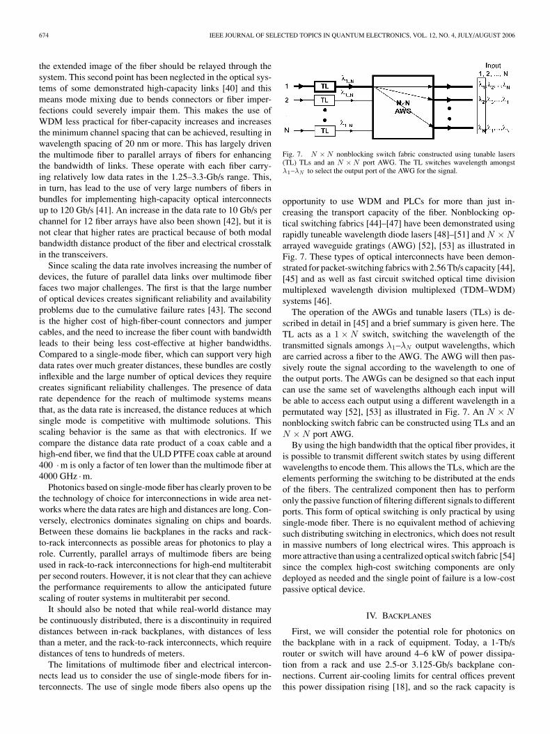
Fig. 7. N × N nonblocking switch fabric constructed using tunable lasers(TL) TLs and an N × N port AWG. The TL switches wavelength amongstλ1–λN to select the output port of the AWG for the signal.
opportunity to use WDM and PLCs for more than just in-creasing the transport capacity of the fiber. Nonblocking op-tical switching fabrics [44]–[47] have been demonstrated usingrapidly tuneable wavelength diode lasers [48]–[51] and N × Narrayed waveguide gratings (AWG) [52], [53] as illustrated inFig. 7. These types of optical interconnects have been demon-strated for packet-switching fabrics with 2.56 Tb/s capacity [44],[45] and as well as fast circuit switched optical time divisionmultiplexed wavelength division multiplexed (TDM–WDM)systems [46].
The operation of the AWGs and tunable lasers (TLs) is de-scribed in detail in [45] and a brief summary is given here. TheTL acts as a 1 × N switch, switching the wavelength of thetransmitted signals amongs λ1–λN output wavelengths, whichare carried across a fiber to the AWG. The AWG will then pas-sively route the signal according to the wavelength to one ofthe output ports. The AWGs can be designed so that each inputcan use the same set of wavelengths although each input willbe able to access each output using a different wavelength in apermutated way [52], [53] as illustrated in Fig. 7. An N × Nnonblocking switch fabric can be constructed using TLs and anN × N port AWG.
By using the high bandwidth that the optical fiber provides, itis possible to transmit different switch states by using differentwavelengths to encode them. This allows the TLs, which are theelements performing the switching to be distributed at the endsof the fibers. The centralized component then has to performonly the passive function of filtering different signals to differentports. This form of optical switching is only practical by usingsingle-mode fiber. There is no equivalent method of achievingsuch distributing switching in electronics, which does not resultin massive numbers of long electrical wires. This approach ismore attractive than using a centralized optical switch fabric [54]since the complex high-cost switching components are onlydeployed as needed and the single point of failure is a low-costpassive optical device.
IV. BACKPLANES
First, we will consider the potential role for photonics onthe backplane with in a rack of equipment. Today, a 1-Tb/srouter or switch will have around 4–6 kW of power dissipa-tion from a rack and use 2.5-or 3.125-Gb/s backplane con-nections. Current air-cooling limits for central offices preventthis power dissipation rising [18], and so the rack capacity is
NEILSON: PHOTONICS FOR SWITCHING AND ROUTING 675
limited by power dissipation. Use of newer generations of sili-con will reduce the power dissipation as discussed above and,therefore, the capacity will rise by only 20% per year. Thedata rate on a trace will also scale at the same rate and soit will take around 10–15 years to get to 40-Gb/s per back-plane trace with rack capacities around 10–16 Tb/s Therefore,data rates of 40 Gb/s are sufficient to meet a single rack’sneeds for the foreseeable future and they seem to be potentiallypractical (see Section III and [15] and [55]) using electronictechniques.
Given that it looks to be practical to construct electrical back-planes to meet the foreseeable needs, the role for a photonicbackplane would be to provide this performance at a lowerpower dissipation. Simulations show that for nonreturn to zero(NRZ) signaling using PCBs with GETEK polymer [35] (with2 dB/m/GHz dielectric loss), the critical length at which thepower dissipation for 6 Gb/s is the same for optical and electri-cal connections is around 40–75 cm. In a similar analysis withFR4 boards (4.5 dB/m/GHz dielectric loss) [37], the criticaldistance and bandwidth was found to be 3.8 GHz at 100 cm,which given the different dielectric losses makes these compa-rable results. Since these distances are comparable to typicalbackplane distances, this initially looks promising for the use ofoptics at 40 Gb/s. However, there are options that can reduce thepower dissipation of the electronic solutions. Since the powerdissipation of optics is nearly independent of distance, the dis-tance at which they have equal power is set by the loss in theelectrical line, which from (2) is proportional to the dielectricloss of the material and the bandwidth of the electrical signal.The use of multilevel signaling [25]–[27] reduces the bandwidthrequirement, and hence, loss by a factor of two for duobinary.The use of even lower loss dielectric materials such as RO4003with 0.6 dB/m/GHz [28] could also further reduce the loss bya factor of 3.3 relative to GETEK [35] and combining lowerbandwidth and lower loss material would increase the data rateby a factor of 6.7. This would set the point at which optics wouldhave comparable dissipation to be in the range of 40 Gb/s acrossa backplane.
There are additional challenges with implementing opticalbackplanes: there is finding appropriate dielectrics for formingoptical waveguides which can be incorporated at low cost withthe electrical lines that will still be required; in maintaining lowloss coupling while avoiding using highly multimode guides,which will result in modal dispersion limits on data rates; thereliability of the optical devices which may require multipletransmitters. Given the challenges that face implementing opti-cal backplanes in a rack and the ability of electronic intercon-nects to meet the foreseeable data capacity needs of such a rackand the absence of a compelling power dissipation advantagefor optics the case for implementing optical backplanes in therack is not very strong.
V. RACK-TO-RACK INTERCONNECTS AND SWITCHING
As we noted earlier, router capacity may be expected to scaleto 100-Tb/s capacity in the next 5–6 years. From power dissipa-tion considerations, each LC rack will have between 3 and 5 Tb/s
of capacity. A single router will, therefore, consist of multipleracks of LCs, of the order of 20–30, plus a similar number forthe switch fabrics. If we consider wiring between racks, we areconsidering distances of tens of meters to potentially hundredsof meters and interconnection capacities of 100 Tb/s or greaterfor multistage architectures. There are now two significant chal-lenges: how to interconnect the racks and how to switch thetraffic between them. While it is pretty clear that optics willplay a role in interconnecting the racks given they are already inuse in 2.5-Tb/s routers [21], [22], there are several options forthe type of optics that could be used and how that might impactswitching.
On the timescale for such a 100-Tb/s router, we might expectTDM line rates on a single-mode fiber to be of the order of100 Gb/s. If we assume 5 Tb/s per rack, the future systemmight consist of LCs each terminating a total of 25 bidirectional100-Gb/s Ethernet. The backplane for each rack would need touse interconnect at around 25 Gb/s per line, for which a high-speed electrical backplane would suffice. To achieve more than100 Tb/s, we would need 20 such racks.
For the interconnect between the racks where optics will playa role, we should first consider the required data rate per fiber.Even at 10 Gb/s per fiber as might be practical with multimodefibers, the bidirectional data rate per rack of 5 Tb/s means thedensity of fibers and transmitters is still very large with 500 perrack. This capacity could be carried on a few single-mode fibersor even the one using DWDM approaches. If we build the rack-to-rack interconnect using 100-Gb/s rates, then each rack wouldhave fifty 100-Gb/s links coming off it. It is clear, therefore, thatif we are to keep the number of transmitters and fibers to manage-able levels, then we need to use high-data rate transmitters. Elec-trical multiplexed optical signaling at 107 Gb/s using duo-binaryhas been recently demonstrated [55]. This format is attractivesince it requires the Mach–Zehnder modulators with around35-GHz 3-dB bandwidth. Such a transmission format shouldallow distances of at least 1 km over standard single-mode fiberwithout the need for dispersion compensation, which is suffi-cient for interconnecting such a router. These transmitters couldalso use a dense photonic integration approach using multipleDWDM transmitters per chip in monolithic InP [57] or some hy-brid technology employing CMOS photonic devices [58], [59].However, although the given line rates on the backplane couldwell be 25 Gb/s by that stage, it is unlikely that that the data rateper transmitter would be below that.
Building switch fabrics for such a router in electronics wouldrepresent a significant challenge [7] and the use of opticalswitching technologies could be used to alleviate this. As de-scribed above and illustrated in Fig. 6, tunable wavelength diodelasers and N × N AWGs provide an attractive way of buildingan optical crossconnect since the only required component atstartup is the AWG, which is a low-cost high-reliability pas-sive component. The more complex elements the wavelengthswitching lasers need only be deployed as the populated fabriccapacity grows.
We will consider the current state of the art in optical switch-ing technologies to assess the level difficulty one might en-counter in constructing future larger switch fabrics. Optical

676 IEEE JOURNAL OF SELECTED TOPICS IN QUANTUM ELECTRONICS, VOL. 12, NO. 4, JULY/AUGUST 2006
switch fabrics with 0.8 b/s/Hz spectral efficiency using 40 Gb/son a 50-GHz channel spacing using optical duo-binary [44]have been shown. Sampled grating distributed Bragg reflec-tor (SG-DBR) lasers have been demonstrated with more than 4THz [60] and digital supermode distributed Bragg reflector (DS-DBR) lasers with 6 THz of tuning range have been demonstrated[61]. Since the frequency-tuning range and spectral efficiencydetermines the maximum switch capacity, it indicates thatswitch fabrics with around 5 Tb/s of capacity should be pos-sible today. Using higher spectral efficiency coding schemes,such as DQPSK, which has been demonstrated at 100 Gb/s [62]and can achieve spectral densities of 1.6 b/s/Hz [63], or polar-ization multiplexing could also increase the switching capacityby another factor of two or four pushing switch fabrics to the10–20-Tb/s capacity. Use of differential phase-encoded formatssuch as DQPSK could pose challenges when combined withwavelength switching since these formats are significantly moresensitive to laser frequency offsets [64]. Increasing the tuningranges of the lasers would similarly increase the capacity ofthe switches. Since TLs have been demonstrated with around30 THz of tuning range [65], there is certainly some prospectof increased tuning range for the lasers for this application.Another challenge for the lasers is in the switching time, andrecently, the SGDBR lasers have been shown to be capable ofbeing switched in less than 5 ns [51].
Considering the current state of these underlying technolo-gies, this approach to building a distributed optical switch fab-ric with close to the 50-Tb/s capacity required for a 100-Tb/srouter looks plausible though some enhancement of existing de-vice technologies would be required. Work on monolithic [66]and copackaged integration [67] of modulators and TLs andthe development of higher data rate modulators [68] also showpromise for making compact high-data-rate tunable transmittersfor the wavelength switching described above.
VI. CONCLUSION
The continued growth of data networks is going to requirehigher capacity packet transport, switching, and routing. We dis-cussed that transport can be scaled through the use of DWDM.Circuit-switched network elements, which are electronic TDMdevices today, can be replaced by ROADMs, which eliminatedthe need to build very large TDM circuit switches. However,packet routers will become the major challenge for networkscaling. We have described some of the challenges that exist forscaling today’s packet routers related to thermal density, inter-connect, and large switching fabrics. We have considered that therole of photonics might play in scaling such routers to 100 Tb/s.
The thermal density is requiring larger routers to be multiracksolutions with a high-capacity interconnect between racks ofLCs and switch fabrics. Within the racks, we do not see a role foroptical interconnects since electronic interconnects are capableof delivering the performance requirements for scaling racks forthe foreseeable future.
The use of multistage electronic switch fabrics, as in today’shigh-end routers, has nonlinear scaling with capacity in the num-ber of switch fabrics and interconnects and both will quickly
become unwieldy. Today in such routers, the interconnect be-tween racks of LCs and switching fabrics uses multimode fiberoptics. With increasing data rates, a transition to single-modefiber for this application will be required.
There is a need to transition to routers in which the switchingis more scaleable and distributed. This can be achieved by usingwavelength switching. The wavelength switching also exploitsthe multiterahertz bandwidth of the optical fiber to encode theswitching states, which uniquely provides improved incrementalscaling. The wavelength switching also reduced the number ofE–O and O–E conversions compared to using an electronicfabric.
This use of fast wavelength switching can be seen as a packetanalog to the use of ROADMs in transparent networking, whichuses wavelength to define the destination of a circuit. But here,we are using wavelength to define the destination of a packet ona per packet basis.
ACKNOWLEDGMENT
The author would like to acknowledge many helpful discus-sions with and comments from his colleagues at Bell Labs,which helped to shape this paper including P. Bernasconi on thescalability of AWGs, with J. Gripp on optical switching usingTLs and AWGs, with J. Simsarian on fast switching of TLs,and with J. Sinsky on the capabilities of electrical signaling onbackplanes.
REFERENCES
[1] A. M. Odlyzko, “The current state and likely evolution of the internet,” inProc. Globecom ’99, 1999, pp. 1869–1875.
[2] , “Internet traffic growth: sources and implications,” in Proc. SPIEOpt. Transmiss. Syst. Equip. WDM Netw. II, 2003, B. B. Dingel, W. Weier-shausen, A. K. Dutta, and K.-I. Sato, Eds., vol. 5247, pp. 1–15.
[3] J. E. Ford, V. A. Aksyuk, D. J. Bishop, and J. A. Walker, “Wavelength add-drop switching using tilting micromirrors,” J. Lightw. Technol., vol. 17,no. 5, pp. 904–911, May 1999.
[4] C. R. Doerr, L. W. Stulz, M. Cappuzzo, E. Laskowski, A. Paunescu,L. Gomez, J. V. Gates, S. Shunk, and A. E. White, “40-wavelength add-drop filter,” IEEE Photon. Technol. Lett., vol. 11, no. 11, pp. 1437–1439,Nov. 1999.
[5] M. P. Earnshaw, M. Cappuzzo, E. Chen, L. Gomez, A. Griffin,E. Laskowski, A. Wong-Foy, and J. Soole, “Planar lightwave circuit basedreconfigurable optical add–drop multiplexer architectures and reusablesubsystem module,” IEEE J. Sel. Topics Quantum Electron., vol. 11,no. 2, pp. 313–322, Mar.–Apr. 2005.
[6] D. T. Neilson, C. R. Doerr, D. M. Marom, R. Ryf, and M. P. Earnshaw,“Wavelength selective switching for optical bandwidth management,”Bell Labs Tech. J., vol. 11, no. 2, pp. 107–130, 2006.
[7] I. Keslassy, S.-T. Chuang, K. Yu, D. Miller, M. Horowitz, O. Solgaard,and N. McKeown, “Scaling internet routers using optics,” presented at theACM SIGCOMM, Karlsruhe, Germany, Aug. 2003.
[8] Router Capacity: Raw Data. [Online]. Available: http://www.stanford.edu/˜nickm/ RouterCapacity.xls
[9] Cisco CRS-1 Multishelf System. [Online]. Available: www.cisco.com[10] C.-S. Chang, D.-S. Lee, and Y.-S. Jou, “Load balanced Birkhof-von Neu-
mann switches—Part I: One-stage buffering,” Comput. Commun., vol. 25,pp. 611–622, 2002.
[11] K. Kar, T. V. Lakshman, D. Stiliadis, and L. Tassiulas, “Reduced com-plexity input buffered switches,” in Proc. Hot Interconnects VIII, 2000,Stanford, CA, pp. 13–20.
[12] I. Keslassy, M. S. Kodialam, T. V. Lakshman, and D. Stiliadis, “On guar-anteed smooth scheduling for input-queued switches,” presented at theINFOCOM, vol. 2, San Francisco, CA, pp. 1384–1394, 2003.

NEILSON: PHOTONICS FOR SWITCHING AND ROUTING 677
[13] I. Keslassy, S.-T. Chuang, and N. McKeown, “Architectures and Algo-rithms for a load-balanced switch,” Stanford Univ., Stanford, CAHPNGTech. Rep. TR03-HPNG-061501, Jun. 2003.
[14] J. E. Simsarian, J. Gripp, M. Duelk, R. Peiro, P. Bernasconi,D. Stiliadis, and M. Zirngibl, “Highly-scalable load-balanced router withoptical switch fabric,” Electron. Lett., vol. 40, no. 25, pp. 1600–1602,2004.
[15] M.-J. E. Lee, W. J. Dally, R. Farjad-Rad, H.-T. Ng, R. Senthinathan,J. Edmondson, and J. Poulton1, “CMOS high-speed I/Os—Present and fu-ture,” in Proc. 21st Int. Conf. Comput. Design, Oct. 13–15, 2003, pp. 454–461.
[16] International Technology Roadmap for Semiconductors: OverallRoadmap Technology Characteristics (ORTC). (2004). [Online]. Avail-able: http://www.itrs.net/Common/2004Update/2004_000_ORTC.pdf
[17] Cisco 12816 Router. [Online]. Available: www.cisco.com[18] N. Rasmussen. (2005, Jan.). Cooling Strategies for Ultra-High
Density Racks and Blade Server APC (WP #46)., [Online].Available: http://www.datacenterjournal.com/Tools/WhitePapers/Power-and-Cooling-for-Ultra-High-Density-Racks-by-APC.pdf
[19] Juniper TX Matrix. [Online]. Available: www.juniper.net[20] C. Clos, “A study of non-blocking switching networks,” Bell Syst. Tech.
J., vol. 32, pp. 406–424, Mar. 1953.[21] T640 routing node and TX matrix platform: Architecture. (2004). [On-
line]. Available: http://www.juniper.net/solutions/literature/white_papers/200089.pdf
[22] TX matrix platform: Hardware components and cable system.(2004). [Online]. Available: http://www.juniper.net/solutions/literature/white_papers/200099.pdf
[23] R. Wood, Next-Generation Network Services. Indianapolis, IN: CiscoPress, Nov. 2005, Indianapolis, IN, ch. 3.
[24] D. Huang, T. Sze, A. Landin, R. Lytel, and H. L. Davidson, “Opticalinterconnects: Out of the box forever?” IEEE J. Sel. Topics QuantumElectron., vol. 9, no. 2, pp. 614–623, Mar.–Apr. 2003.
[25] Y. Hur, M. Maeng, S. Chandramouli, F. Bien, E. Gebara1, K. Lim,and J. Laskar, “4-PAM/20Gbps transmission over 20-in FR-4 backplanechannels: Channel characterization and system implementation,” in Proc.IMAPS Tech. Workshop, Palo Alto, CA, Oct. 2003.
[26] C. Menolfi, T. Toifl, R. Reutemann, M. Ruegg, P. Buchmann, M. Kossel,T. Morf, and M. Schmatz, “A 25 Gb/s PAM4 transmitter in 90 nm CMOSSOI,” in Proc. IEEE ISSCC, Feb. 6–10, 2005, vol. 1, pp. 77–78.
[27] J. H. Sinsky, M. Duelk, and A. Adamiecki, “High-speed electrical back-plane transmission using duobinary signaling,” IEEE Trans. Microw.Theory Tech., vol. 53, no. 1, pp. 152–160, Jan. 2005.
[28] “Advance circuit materials.” [Online]. Available: http://www.rogerscorporation.com/mwu/pdf/ro4000 ds_4.pdf
[29] M. Resso, M. Canestrano, and N. Smith, “Investigating microvia technol-ogy for 10 Gbps and higher telecommunication systems,” in Design ConnEast 2005 Tuesday, September 20|9:20 am–10:00 am. [Online]. Avail-able: http://cp.literature.agilent.com/litweb/pdf/5989-2422EN.pdf, [On-line]. Available:
[30] UTiFLEX Flexible Microwave Cable Assemblies UFB142A. [Online].Available: www.micro-coax.com
[31] J. Sinsky. (2005, Oct.). Private communication.[32] B. M. Oliver, “Thermal and quantum noise,” Proc. IEEE, vol. 53, no. 5,
pp. 436–454, May 1965.[33] D. A. B. Miller, “Optics for low energy communications inside digi-
tal processors: Quantum detectors, sources and modulators as efficientimpedance converters,” Opt. Lett., vol. 14, p. 146, 1989.
[34] E. Berglind, L. Thylen, B. Jaskorzynska, and C. Svensson, “A compar-ison of dissipated power and signal-to-noise ratios in electrical and op-tical interconnects,” J. Lightw. Technol., vol. 17, no. 1, pp. 68–73, Jan.1999.
[35] H. Cho, P. Kapur, and K. C. Saraswat, “Power comparison between high-speed electrical and optical interconnects for interchip communication,”J. Lightw. Technol., vol. 22, no. 9, pp. 2021–2033, Sep. 2004.
[36] , “The impact of technology on power for high-speed electrical andoptical interconnects,” in Proc. IEEE Int. Conf. Interconnect Technol.,Jun. 6–8, 2005, pp. 177–179.
[37] E. Yuceturk, S. C. Esener, D. Huang, and T. Sze, “Comparative study ofvery short distance electrical and optical interconnects based on channelcharacteristics,” in Optics in Computing (Trends in Optics and PhotonicsSeries 90), Washington, DC: Optical Society of America, Jun. 2003, pp. 7–9., (Trends in Optics and Photonics Series 90), Optical Society of America
[38] “LaserWave TM 550-330 fibers.” [Online]. Available: http://www.ofsoptics.com/resources/LaserWave550-330web.pdf
[39] D. T. Neilson and E. Schenfeld, “Free-space optical relay for intercon-nection of multimode fibers,” Appl. Opt., vol. 38, no. 8, pp. 2291–2296,1999.
[40] B. E. Lemoff, M. E. Ali, G. Panotopoulos, E. de Groot, G. M. Flower,G. H. Rankin, A. J. Schmit, K. D. Djordjev, M. R. T. Tan, A. Tandon,W. Gong, R. P. Tella, B. Law, and D. W. Dolfi, “500-Gbps parallel-WDMoptical interconnect,” in Proc. ECTC ’05, May 31–Jun. 3, 2005, pp. 1027–1031.
[41] C. Cook, J. E. Cunningham, A. Hargrove, G. G. Ger, K. W. Goossen,W. Y. Jan, H. H. Kim, R. Krause, M. Manges, M. Morrissey,M. Perinpanayagam, A. Persaud, G. J. Shevchuk, V. Sinyansky, andA. V. Krishnamoorthy, “A 36-channel parallel optical interconnect mod-ule based on optoelectronics-on-VLSI technology,” IEEE J. Sel. TopicsQuantum Electron., vol. 9, no. 2, pp. 387–399, Mar.–Apr. 2003.
[42] D. M. Kuchta, Y. H. Kwark, C. Schuster, C. Baks, C. Haymes, J. Schaub,P. Pepeljugoski, L. Shan, R. John, D. Kucharski, D. Rogers, M. Ritter,J. Jewell, L. A. Graham, K. Schrodinger, A. Schild, and H.-M. Rein,“120-Gb/s VCSEL-based parallel-optical interconnect and custom 120-Gb/s testing station,” J. Lightw. Technol., vol. 22, no. 9, pp. 2200–2212,Sep. 2004.
[43] A. V. Krishnamoorthy, D. Huang, T. Sze, R. Drost, R. Ho, H. Davidson,and R. Lytel, “Challenges and potentials for multiterabit-per-second op-tical transceivers,” in Proc. Digest LEOS Summer Topical Meetings Bio-photon./Opt. Interconnects VLSI Photon./WBM Microcavities, Jun. 28–30,2004, p. 2.
[44] M. Duelk, J. Gripp, J. Simsarin, A. Bhardwaj, P. Bernasconi, M. Zirngibl,and O. Laznicka, “Fast packet routing in a 2.5 Tb/s optical switch fabricwith 40 Gb/s duobinary signal at 0.8 b/s/Hz spectral efficiency,” in Proc.Opt. Fiber Commun. Conf. Expo., 2003, pp. PD8-1–PD8-3.
[45] J. Gripp, M. Duelk, J. Simsarian, A. Bhardwaj, P. Bernasconi, O. Laznicka,and M. Zirngibl, “Optical switch fabrics for ultra-high capacity IP-routers,” IEEE J. Lightw. Technol., vol. 21, no. 11, pp. 2839–2850, Nov.2003.
[46] J. Gripp, M. Duelk, J. Simsarian, and M. Zirngibl, “Demonstration ofsynchronous traffic transport over a time-multiplexed WDM ring,” inProc. OFC, Feb. 23–27, 2004, vol. 2, p. 3.
[47] J. Gripp, M. Duelk, J. Simsarian, S. Chandrasekhar, P. Bernasconi,A. Bhardwaj, Y. Su, K. Sherman, L. Buhl, E. Laskowski, M. Capuzzo,L. Stulz, M. Zirngibl, O. Laznicka, T. Link, R. Seitz, P. Mayer, andM. Berger, “Demonstration of a 1.2 Tb/s optical packet switch fabric(32× 40 Gb/s) based on 40 Gb/s burst-mode clock-data-recovery, fast tun-able lasers and a high-performance NxN AWG,” in Proc. 27th ECOC ’01,2001, vol. 6, pp. 58–59.
[48] J. E. Simsarian, A. Bhardwaj, J. Gripp, K. Sherman, Y. Su, C. Webb,L. Zhang, and M. Zirngibl, “Fast switching characteristics of a widelytunable laser transmitter,” IEEE Photon. Technol. Lett., vol. 15, no. 8,pp. 1038–1040, Aug. 2003.
[49] A. Bhardwaj, J. Gripp, J. E. Simsarian, and M. Zirngibl, “Demonstrationof stable wavelength switching on a fast tunable laser transmitter,” IEEEPhoton. Technol. Lett., vol. 15, no. 7, pp. 1014–1016, Jul. 2003.
[50] R. Monnard, M. Zirngibl, C. R. Doerr, C. Joyner, and L. W. Stulz, “Demon-stration of an eight-wavelength fast packet switching transmitter of 2.5-Gb/s bit stream,” IEEE Photon. Technol. Lett., vol. 10, no. 3, pp. 430–432,Mar. 1998.
[51] J. E. Simsarian, M. C. Larson, H. E. Garrett, H. Xiu, and T. A. Strand,“Less than 5 ns wavelength switching with an SG-DBR laser,” IEEEPhoton. Technol. Lett., vol. 18, no. 4, pp. 565–567, Feb. 2006.
[52] C. Dragone, “An N×N optical multiplexer using a planar arrangement oftwo star couplers,” IEEE Photon. Technol. Lett., vol. 3, no. 9, pp. 812–815,Sep. 1991.
[53] P. Bernasconi, C. R. Doerr, C. Dragone, M. Capuzzo, E. Laskowski,and A. Paunescu, “Large N×N waveguide grating routers,” J. Lightw.Technol., vol. 18, no. 7, pp. 985–991, Jul. 2000.
[54] E. Shekel, A. Feingold, Z. Fradkin, A. Geron, J. Levy, G. Matmon,D. Majer, E. Rafaely, M. Rudman, G. Tidhar, J. Vecht, and S. Ruschin,“64× 64 fast optical switching module,” in Proc. OFC (OSA Trends inOptics and Photonics Series 70), 2002, pp. 27–29, Paper TuF3, (OSATrends in Optics and Photonics Series 70), Paper TuF3
[55] D. Hwang, T. Sze, A. Landin, R. Lytel, and H. L. Davidson, “Opticalinterconnects: Out of the box forever?” J. Sel. Topics Quantum Electron.,vol. 9, no. 2, pp. 614–623, Mar. 2003.
[56] P. J. Winzer, G. Raybon, and M. Duelk, “107-Gb/s optical ETDM trans-mitter for 100G ethernet transport,” presented at the 31st Eur. Conf. onOptical Communications (ECOC), Glasgow, U.K., Sep. 26–28, 2005,paper 4.1.1.

678 IEEE JOURNAL OF SELECTED TOPICS IN QUANTUM ELECTRONICS, VOL. 12, NO. 4, JULY/AUGUST 2006
[57] R. Nagarajan, C. H. Joyner, R. P. Schneider, Jr., J. S. Bostak, T. Butrie,A. G. Dentai, V. G. Dominic, P. W. Evans, M. Kato, M. Kauffman,D. J. H. Lambert, S. K. Mathis, A. Mathur, R. H. Miles, M. L. Mitchell,M. J. Missey, S. Murthy, A. C. Nilsson, F. H. Peters, S. C. Pennypacker,J. L. Pleumeekers, R. A. Salvatore, R. K. Schlenker, R. B. Taylor,T. Huan-Shang, M. F. Van Leeuwen, J. Webjorn, M. Ziari, D. Perkins,J. Singh, S. G. Grubb, M. S. Reffle, D. G. Mehuys, F. A. Kish,and D. F. Welch, “Large-scale photonic integrated circuits,” IEEE J.Sel. Topics Quantum Electron., vol. 11, no. 1, pp. 50–65, Jan.–Feb.2005.
[58] C. Gunn, “Photonics integration for optical interconnects,” in Proc. 18thIEEE LEOS Annu. Meeting, Oct. 23–27, 2005, p. 732.
[59] C. Gunn. (2005). CMOS photonics technology—Enabling optical in-terconnects. in Proc. HOT CHIPS 17., [Online]. Available: http://www.hotchips.org/archives/hc17/2_Mon/HC17.S3/HC17.S3T1.pdf
[60] B. Mason, J. Barton, G. A. Fish, L. A. Coldren, and S. P. DenBaars,“Design of sampled grating DBR lasers with integrated semiconductoroptical amplifiers,” IEEE Photon. Technol. Lett., vol. 12, no. 7, pp. 762–764, Jul. 2000.
[61] J. P. Duck, L. Ponnampalam, A. J. Ward, D. J. Robbins, G. Busico,N. D. Whitbread, and D. C. J. Reid, “Design and analysis of DS-DBR lasers for C and L-Band, achieving a combined count of over 200consecutive 50 GHz spaced channels,” presented at the 31st Eur. Conf.on Optical Communications (ECOC), Glasgow, U.K., Sep. 26–28, 2005,Paper 2.5.4.
[62] M. Daikoku, I. Morita, H. Taga, H. Tanaka, T. Kawanishi, T. Sakamoto,T. Miyazaki, and T. Fujita, “100Gb/s DQPSK transmission experimentwithout OTDM for 100G ethernet transport,” in Proc. OFC, Aneheim,CA, 2006, pp. 1–3.
[63] C. Wree, N. Hecker-Denschlag, E. Gottwald, P. Krummrich, J. Leibrich,E. D. Schmidt, B. Lankl, and W. Rosenkranz, “High spectral efficiency1.6-b/s/Hz transmission (8× 40 Gb/s with a 25-GHz grid) over 200-kmSSMF using RZ-DQPSK and polarization multiplexing,” IEEE Photon.Technol. Lett., vol. 15, no. 9, pp. 1303–1305, Sep. 2003.
[64] H. Kim and P. J. Winzer, “Robustness to laser frequency offset in direct-detection DPSK and DQPSK systems,” J. Lightw. Technol., vol. 21, no. 9,pp. 1887–1891, Sep. 2003.
[65] H. Tabuchi and H. Ishikawa, “External grating tunable MQW laser withwide tuning range of 240 nm,” Electron. Lett., vol. 26, pp. 742–743, 1990.
[66] Y. A. Akulova, G. A. Fish, P. Koh, P. Kozodoy, M. Larson, C. Schow,E. Hall, H. Marchand, P. Abraham, and L. A. Coldren, “10 Gb/sMach-Zehnder modulator integrated with widely-tunable sampled grat-ing DBR laser,” in Proc. OFC, Feb. 2004, vol. 1, pp. 23–27.
[67] R. A. Griffin, B. Pugh, J. Fraser, G. Busico, C. Edge, T. Simmons,I. B. Betty, and K. Anderson, “Compact, high power, MQW InP Mach-Zehnder transmitters with full-band tunability for 10 Gb/s DWDM,” pre-sented at the Eur. Conf. Optical Communications (ECOC), 2005, PaperTh2.6.2.
[68] K. Tsuzuki, H. Kikuchi, E. Yamada, H. Yasaka, and T. Ishibashi, “1.3-Vpp push-pull drive InP Mach-Zehnder modulator module for 40 Gbit/soperation,” presented at the Eur. Conf. Optical Communications (ECOC),2005, Paper Th2.6.3.
David T. Neilson (M’96–SM’02) received the B.Sc. (honors) and Ph.D. degreesfrom Heriot-Watt University, Edinburgh, U.K., in 1990 and 1993, respectively,both in physics.
From 1993 to 1996, he was a Postdoctoral Researcher at Heriot-Watt Uni-versity,working on systems and devices for free-space optical interconnectsand switching. From 1996 to 1998, he was a Visiting Scientist at the NECResearch Institute, Princeton, NJ, researching optical interconnects for high-performance computing. In 1998, he joined Bell Laboratories, Holmdel, NJ,where he has worked on MEMS-based crossconnects, wavelength selectiveswitches, equalizers, and dispersion compensators, and where he is currently aTechnical Manager leading a group conducting research on highly integratedInP-based optoelectronic components and subsystems and has responsibility foroptoelectronic device growth and fabrication facility. He has authored over 110publications and is the holder of 17 issued patents in the field of optical intercon-nects, switching, and optoelectronic devices. His research interests include therole of optical interconnects and switching for high-capacity optical switchesand routers.
Dr. Neilson is a Senior Member of the IEEE Lasers and Electro-optics Soci-ety and a member of the Optical Society of America.