Embed Size (px)
Citation preview

S.O. Kasap, Optoelectronics and Photonics: Principles and Practices, Second Edition, © 2013 Pearson Education© 2013 Pearson Education, Inc., Upper Saddle River, NJ. All rights reserved. This publication is protected by Copyright and written permission should be obtained from the
publisher prior to any prohibited reproduction, storage in a retrieval system, or transmission in any form or by any means, electronic, mechanical, photocopying, recording, or likewise. For information regarding permission(s), write to: Rights and Permissions Department, Pearson Education, Inc., Upper Saddle River, NJ 07458.
Power Point for Optoelectronics and Photonics: Principles and Practices
Second Edition
ISBN-10: 0133081753Second Edition Version 1.0571 [8 February 2015]
A Complete Course in Power Point
Chapter 2
S.O. Kasap, Optoelectronics and Photonics: Principles and Practices, Second Edition, © 2013 Pearson Education© 2013 Pearson Education, Inc., Upper Saddle River, NJ. All rights reserved. This publication is protected by Copyright and written permission should be obtained from the
publisher prior to any prohibited reproduction, storage in a retrieval system, or transmission in any form or by any means, electronic, mechanical, photocopying, recording, or likewise. For information regarding permission(s), write to: Rights and Permissions Department, Pearson Education, Inc., Upper Saddle River, NJ 07458.
Updates andCorrected Slides
Class Demonstrations
Class Problems
Check author’s websitehttp://optoelectronics.usask.ca
Email errors and corrections to [email protected]

Slides on Selected Topics on
Optoelectronics
may be available at the author website
http://optoelectronics.usask.ca
Email errors and corrections to [email protected]

S.O. Kasap, Optoelectronics and Photonics: Principles and Practices, Second Edition, © 2013 Pearson Education© 2013 Pearson Education, Inc., Upper Saddle River, NJ. All rights reserved. This publication is protected by Copyright and written permission should be obtained from the
publisher prior to any prohibited reproduction, storage in a retrieval system, or transmission in any form or by any means, electronic, mechanical, photocopying, recording, or likewise. For information regarding permission(s), write to: Rights and Permissions Department, Pearson Education, Inc., Upper Saddle River, NJ 07458.
This Power Point presentation is a copyrighted supplemental material to the textbookOptoelectronics and Photonics: Principles & Practices, Second Edition, S. O. Kasap,Pearson Education (USA), ISBN-10: 0132151499, ISBN-13: 9780132151498. © 2013Pearson Education. Permission is given to instructors to use these Power Point slides intheir lectures provided that the above book has been adopted as a primary requiredtextbook for the course. Slides may be used in research seminars at research meetings,symposia and conferences provided that the author, book title, and copyright informationare clearly displayed under each figure. It is unlawful to use the slides for teaching if thetextbook is not a required primary book for the course. The slides cannot be distributedin any form whatsoever, especially on the internet, without the written permission ofPearson Education.
Copyright Information and Permission: Part I
Please report typos and errors directly to the author: [email protected]

S.O. Kasap, Optoelectronics and Photonics: Principles and Practices, Second Edition, © 2013 Pearson Education© 2013 Pearson Education, Inc., Upper Saddle River, NJ. All rights reserved. This publication is protected by Copyright and written permission should be obtained from the
publisher prior to any prohibited reproduction, storage in a retrieval system, or transmission in any form or by any means, electronic, mechanical, photocopying, recording, or likewise. For information regarding permission(s), write to: Rights and Permissions Department, Pearson Education, Inc., Upper Saddle River, NJ 07458.
This Power Point presentation is a copyrighted supplemental material to the textbookOptoelectronics and Photonics: Principles & Practices, Second Edition, S. O. Kasap,Pearson Education (USA), ISBN-10: 0132151499, ISBN-13: 9780132151498. © 2013Pearson Education. The slides cannot be distributed in any form whatsoever,electronically or in print form, without the written permission of Pearson Education. It isunlawful to post these slides, or part of a slide or slides, on the internet.
Copyright © 2013, 2001 by Pearson Education, Inc., Upper Saddle River, New Jersey,07458. All rights reserved. Printed in the United States of America. This publication isprotected by Copyright and permission should be obtained from the publisher prior toany prohibited reproduction, storage in a retrieval system, or transmission in any form orby any means, electronic, mechanical, photocopying, recording, or likewise. Forinformation regarding permission(s), write to: Rights and Permissions Department.
Copyright Information and Permission: Part II
PEARSON

S.O. Kasap, Optoelectronics and Photonics: Principles and Practices, Second Edition, © 2013 Pearson Education© 2013 Pearson Education, Inc., Upper Saddle River, NJ. All rights reserved. This publication is protected by Copyright and written permission should be obtained from the
publisher prior to any prohibited reproduction, storage in a retrieval system, or transmission in any form or by any means, electronic, mechanical, photocopying, recording, or likewise. For information regarding permission(s), write to: Rights and Permissions Department, Pearson Education, Inc., Upper Saddle River, NJ 07458.
Important NoteYou may use color illustrations from this Power Point in your research-related seminars or research-related
presentations at scientific or technical meetings, symposia or conferences provided that you fully cite
the following reference under each figure
From: S.O. Kasap, Optoelectronics and Photonics: Principles and Practices, Second Edition, © 2013 Pearson Education, USA

S.O. Kasap, Optoelectronics and Photonics: Principles and Practices, Second Edition, © 2013 Pearson Education© 2013 Pearson Education, Inc., Upper Saddle River, NJ. All rights reserved. This publication is protected by Copyright and written permission should be obtained from the
publisher prior to any prohibited reproduction, storage in a retrieval system, or transmission in any form or by any means, electronic, mechanical, photocopying, recording, or likewise. For information regarding permission(s), write to: Rights and Permissions Department, Pearson Education, Inc., Upper Saddle River, NJ 07458.
Chapter 2 Dielectric Waveguides and Optical Fibers
Charles Kao, Nobel Laureate (2009)Courtesy of the Chinese University of Hong Kong

S.O. Kasap, Optoelectronics and Photonics: Principles and Practices, Second Edition, © 2013 Pearson Education© 2013 Pearson Education, Inc., Upper Saddle River, NJ. All rights reserved. This publication is protected by Copyright and written permission should be obtained from the
publisher prior to any prohibited reproduction, storage in a retrieval system, or transmission in any form or by any means, electronic, mechanical, photocopying, recording, or likewise. For information regarding permission(s), write to: Rights and Permissions Department, Pearson Education, Inc., Upper Saddle River, NJ 07458.
“The introduction of optical fiber systems will revolutionize the communications network. The low-transmission loss and the large bandwidth capability of the fiber systems allow signals to be transmitted for establishing communications contacts over large distances with few or no provisions of intermediate amplification.” [Charles K. Kao (one of the pioneers of glass fibers for optical communications) Optical Fiber Systems: Technology, Design, and Applications (McGraw-Hill Book Company, New York, USA, 1982), p. 1]
Dielectric Waveguides and Optical Fibers
Courtesy of the Chinese University of Hong Kong
Charles Kao at the naming ceremony of Minor Planet (3463) "Kaokuen" by Nanjing's Purple Mountain Observatory in July 1996. Charles Kao and his colleagues carried out the early experiments on optical fibers at the Standard Telecommunications Laboratories Ltd (the research center of Standard Telephones and Cables) at Harlow in the United Kingdom, during the 1960s. He shared the Nobel Prize in 2009 in Physics with Willard Boyle and George Smith for "groundbreaking achievements concerning the transmission of light in fibers for optical communication." In a milestone paper with George Hockam published in the IEE Proceedings in 1966 they predicted that the intrinsic losses of glass optical fibers could be much lower than 20 dB/km, which would allow their use in long distance telecommunications. Today, optical fibers are used not only in telecommunications but also in various other technologies such as instrumentation and sensing. From 1987 to his retirement in 1996, professor Kao was the Vice Chancellor of the Chinese University of Hong Kong.(Courtesy of the Chinese University of Hong Kong.)

S.O. Kasap, Optoelectronics and Photonics: Principles and Practices, Second Edition, © 2013 Pearson Education© 2013 Pearson Education, Inc., Upper Saddle River, NJ. All rights reserved. This publication is protected by Copyright and written permission should be obtained from the
publisher prior to any prohibited reproduction, storage in a retrieval system, or transmission in any form or by any means, electronic, mechanical, photocopying, recording, or likewise. For information regarding permission(s), write to: Rights and Permissions Department, Pearson Education, Inc., Upper Saddle River, NJ 07458.
Light is guided along a water jet as demonstrated by Jean-Daniel Colladon. This illustration was published in La Nature, Revue des Sciences, in 1884 (p. 325). His first demonstration was around 1841. (Comptes Rendes, 15, 800-802, Oct. 24, 1842). A similar demonstration was done by John Tyndall for the Royal Institution in London in his 1854 lecture. Apparently, Michael Faraday had originally suggested the experiment to John Tyndall though Faraday himself probably learned about it either from another earlier demonstration or through Jean-Daniel Colladon's publication. Although John Tyndall is often credited with the original discovery of a water-jet guiding light, Tyndall, himself, does not make that claim but neither does he attribute it to someone else. (The fountain, courtesy of Conservatoire Numérique des Arts et Métiers, France; Colladon's portrait, courtesy of Musée d'histoire des sciences, Genève, Switzerland.)
Reference: Jeff Hecht, "Illuminating the Origin of Light Guiding," Optics & Photonics News, 10, 26, 1999 and his wonderful book The City of Light (Oxford University Press, 2004) describe the evolution of the optical fiber from the water jet experiments of Colladon and Tyndall to modern fibers with historical facts and references.
1841
Jean-Daniel Colladon and the Light Guiding in a Water Jet

S.O. Kasap, Optoelectronics and Photonics: Principles and Practices, Second Edition, © 2013 Pearson Education© 2013 Pearson Education, Inc., Upper Saddle River, NJ. All rights reserved. This publication is protected by Copyright and written permission should be obtained from the
publisher prior to any prohibited reproduction, storage in a retrieval system, or transmission in any form or by any means, electronic, mechanical, photocopying, recording, or likewise. For information regarding permission(s), write to: Rights and Permissions Department, Pearson Education, Inc., Upper Saddle River, NJ 07458.
Narinder Singh KapanyNarinder Singh Kapany was born in Punjab in India, studied at the Agra University and then obtained his PhD from the Imperial College of Science and Technology, University of London in 1955. He held a number of key-positions in both academia and industry, including a Regents Professor at the University of California, Berkeley, the University of California, Santa Cruz (UCSC), the Director of the Center for Innovation and Entrepreneurial Development at UCSC. He made significant contributions to optical glass fibers starting in 1950s, and essentially coined the term fiber optics in the 1960s. His book Fibre Optics: Principles and Applications, published in 1967, was the first in optical fibers. (Courtesy of Dr. Narinder S. Kapany)

S.O. Kasap, Optoelectronics and Photonics: Principles and Practices, Second Edition, © 2013 Pearson Education© 2013 Pearson Education, Inc., Upper Saddle River, NJ. All rights reserved. This publication is protected by Copyright and written permission should be obtained from the
publisher prior to any prohibited reproduction, storage in a retrieval system, or transmission in any form or by any means, electronic, mechanical, photocopying, recording, or likewise. For information regarding permission(s), write to: Rights and Permissions Department, Pearson Education, Inc., Upper Saddle River, NJ 07458.
A Century and Half Later
Light has replaced copper in communications. Photons have replaced electrons.
Will “Photonics Engineering” replace Electronics Engineering?

S.O. Kasap, Optoelectronics and Photonics: Principles and Practices, Second Edition, © 2013 Pearson Education© 2013 Pearson Education, Inc., Upper Saddle River, NJ. All rights reserved. This publication is protected by Copyright and written permission should be obtained from the
publisher prior to any prohibited reproduction, storage in a retrieval system, or transmission in any form or by any means, electronic, mechanical, photocopying, recording, or likewise. For information regarding permission(s), write to: Rights and Permissions Department, Pearson Education, Inc., Upper Saddle River, NJ 07458.
WAVELENGTH DIVISION MULTIPLEXING: WDM

S.O. Kasap, Optoelectronics and Photonics: Principles and Practices, Second Edition, © 2013 Pearson Education© 2013 Pearson Education, Inc., Upper Saddle River, NJ. All rights reserved. This publication is protected by Copyright and written permission should be obtained from the
publisher prior to any prohibited reproduction, storage in a retrieval system, or transmission in any form or by any means, electronic, mechanical, photocopying, recording, or likewise. For information regarding permission(s), write to: Rights and Permissions Department, Pearson Education, Inc., Upper Saddle River, NJ 07458.
Planar Optical Waveguide
A planar dielectric waveguide has a central rectangular region of higherrefractive index n1 than the surrounding region which has a refractiveindex n2. It is assumed that the waveguide is infinitely wide and thecentral region is of thickness 2a. It is illuminated at one end by a nearlymonochromatic light source.

S.O. Kasap, Optoelectronics and Photonics: Principles and Practices, Second Edition, © 2013 Pearson Education© 2013 Pearson Education, Inc., Upper Saddle River, NJ. All rights reserved. This publication is protected by Copyright and written permission should be obtained from the
publisher prior to any prohibited reproduction, storage in a retrieval system, or transmission in any form or by any means, electronic, mechanical, photocopying, recording, or likewise. For information regarding permission(s), write to: Rights and Permissions Department, Pearson Education, Inc., Upper Saddle River, NJ 07458.
Light waves zigzag along the guide. Is that really what happens?
Optical Waveguide

S.O. Kasap, Optoelectronics and Photonics: Principles and Practices, Second Edition, © 2013 Pearson Education© 2013 Pearson Education, Inc., Upper Saddle River, NJ. All rights reserved. This publication is protected by Copyright and written permission should be obtained from the
publisher prior to any prohibited reproduction, storage in a retrieval system, or transmission in any form or by any means, electronic, mechanical, photocopying, recording, or likewise. For information regarding permission(s), write to: Rights and Permissions Department, Pearson Education, Inc., Upper Saddle River, NJ 07458.
A light ray traveling in the guide must interfere constructively with itself to propagate successfully. Otherwise destructive interference will destroy the wave. E is parallel to x. (λ1 and k1 are the wavelength and the propagation
constant inside the core medium n1 i.e. λ1 = λ/n1.)
Waves Inside the Core

S.O. Kasap, Optoelectronics and Photonics: Principles and Practices, Second Edition, © 2013 Pearson Education© 2013 Pearson Education, Inc., Upper Saddle River, NJ. All rights reserved. This publication is protected by Copyright and written permission should be obtained from the
publisher prior to any prohibited reproduction, storage in a retrieval system, or transmission in any form or by any means, electronic, mechanical, photocopying, recording, or likewise. For information regarding permission(s), write to: Rights and Permissions Department, Pearson Education, Inc., Upper Saddle River, NJ 07458.
Two arbitrary waves 1 and 2 that are initially in phase must remain in phase after reflections. Otherwise the two will interfere destructively and
cancel each other.
Waves Inside the Core

S.O. Kasap, Optoelectronics and Photonics: Principles and Practices, Second Edition, © 2013 Pearson Education© 2013 Pearson Education, Inc., Upper Saddle River, NJ. All rights reserved. This publication is protected by Copyright and written permission should be obtained from the
publisher prior to any prohibited reproduction, storage in a retrieval system, or transmission in any form or by any means, electronic, mechanical, photocopying, recording, or likewise. For information regarding permission(s), write to: Rights and Permissions Department, Pearson Education, Inc., Upper Saddle River, NJ 07458.
k1 = kn1 = 2πn1/λ,
∆φ(AC) = k1(AB + BC) − 2φ = m(2π)
BC = d/cosθ and AB = BCcos(2θ)
AB + BC = BCcos(2θ) + BC = BC[(2cos2θ −1) + 1] = 2dcosθ
k1[2dcosθ] − 2φ = m(2π)
Waveguide condition
πφθλ
π manmm =−
cos)2(2 1
Waveguide ConditionandModes
m = 0, 1, 2, 3 etcInteger
“Mode number”

S.O. Kasap, Optoelectronics and Photonics: Principles and Practices, Second Edition, © 2013 Pearson Education© 2013 Pearson Education, Inc., Upper Saddle River, NJ. All rights reserved. This publication is protected by Copyright and written permission should be obtained from the
publisher prior to any prohibited reproduction, storage in a retrieval system, or transmission in any form or by any means, electronic, mechanical, photocopying, recording, or likewise. For information regarding permission(s), write to: Rights and Permissions Department, Pearson Education, Inc., Upper Saddle River, NJ 07458.
mmmnk θ
λπ
θβ sin2sin 11
==
mmmnk θ
λπθκ cos2cos 1
1
==
Propagation constant along the guide
Transverse Propagation constant

S.O. Kasap, Optoelectronics and Photonics: Principles and Practices, Second Edition, © 2013 Pearson Education© 2013 Pearson Education, Inc., Upper Saddle River, NJ. All rights reserved. This publication is protected by Copyright and written permission should be obtained from the
publisher prior to any prohibited reproduction, storage in a retrieval system, or transmission in any form or by any means, electronic, mechanical, photocopying, recording, or likewise. For information regarding permission(s), write to: Rights and Permissions Department, Pearson Education, Inc., Upper Saddle River, NJ 07458.
Waveguide Condition and Waveguide Modes
To get a propagating wave along a guide you must have constructive interference. All these rays interfere with each other. Only certain angles are allowed . Each allowed angle represents a mode of propagation.
2πn1(2a)λ
cosθm −φm = mπ

S.O. Kasap, Optoelectronics and Photonics: Principles and Practices, Second Edition, © 2013 Pearson Education© 2013 Pearson Education, Inc., Upper Saddle River, NJ. All rights reserved. This publication is protected by Copyright and written permission should be obtained from the
publisher prior to any prohibited reproduction, storage in a retrieval system, or transmission in any form or by any means, electronic, mechanical, photocopying, recording, or likewise. For information regarding permission(s), write to: Rights and Permissions Department, Pearson Education, Inc., Upper Saddle River, NJ 07458.
m = integer, n1 = core refractive index, θm is the incidence angle, 2a is the core thickness.
Minimum θm and maximum m must still satisfy TIR.
There are only a finite number of modes.
Propagation along the guide for a mode m is
mmmnk θ
λπθβ sin2sin 1
1
==
πφθλ
π manmm =−
cos)2(2 1
Waveguide Condition

S.O. Kasap, Optoelectronics and Photonics: Principles and Practices, Second Edition, © 2013 Pearson Education© 2013 Pearson Education, Inc., Upper Saddle River, NJ. All rights reserved. This publication is protected by Copyright and written permission should be obtained from the
publisher prior to any prohibited reproduction, storage in a retrieval system, or transmission in any form or by any means, electronic, mechanical, photocopying, recording, or likewise. For information regarding permission(s), write to: Rights and Permissions Department, Pearson Education, Inc., Upper Saddle River, NJ 07458.
Waveguide Condition and Modes
To get a propagating wave along a guide you must have constructive interference. All these rays interfere with each other. Only certain angles are allowed . Each allowed angle represents a mode of propagation.
2πn1(2a)λ
cosθm −φm = mπ

S.O. Kasap, Optoelectronics and Photonics: Principles and Practices, Second Edition, © 2013 Pearson Education© 2013 Pearson Education, Inc., Upper Saddle River, NJ. All rights reserved. This publication is protected by Copyright and written permission should be obtained from the
publisher prior to any prohibited reproduction, storage in a retrieval system, or transmission in any form or by any means, electronic, mechanical, photocopying, recording, or likewise. For information regarding permission(s), write to: Rights and Permissions Department, Pearson Education, Inc., Upper Saddle River, NJ 07458.
Modes in a Planar Waveguide
E(y,z,t) = Em(y)cos(ωt − βmz)Traveling wave along z
Field pattern along y
We can identify upward (A) and downward (B) traveling waves in the guide which interfere to set up a standing wave along y and a wave that is propagating along z. Rays 2 and 2′ belong to the
same wave front but 2′ becomes reflected before 2. The interference of 1 and 2′ determines the field at a height y from the guide center. The field E(y, z, t) at P can be written as

S.O. Kasap, Optoelectronics and Photonics: Principles and Practices, Second Edition, © 2013 Pearson Education© 2013 Pearson Education, Inc., Upper Saddle River, NJ. All rights reserved. This publication is protected by Copyright and written permission should be obtained from the
publisher prior to any prohibited reproduction, storage in a retrieval system, or transmission in any form or by any means, electronic, mechanical, photocopying, recording, or likewise. For information regarding permission(s), write to: Rights and Permissions Department, Pearson Education, Inc., Upper Saddle River, NJ 07458.
m = integer, n1 = core refractive index, θm is the incidence angle, 2a is the core thickness.
βm = k1 sinθm =2πn1
λ
sinθm
2πn1(2a)λ
cosθm −φm = mπ
Modes in a Planar Waveguide: Summary
E(y,z,t) = Em(y)cos(ωt − βmz)
Traveling wave along zField pattern along y

S.O. Kasap, Optoelectronics and Photonics: Principles and Practices, Second Edition, © 2013 Pearson Education© 2013 Pearson Education, Inc., Upper Saddle River, NJ. All rights reserved. This publication is protected by Copyright and written permission should be obtained from the
publisher prior to any prohibited reproduction, storage in a retrieval system, or transmission in any form or by any means, electronic, mechanical, photocopying, recording, or likewise. For information regarding permission(s), write to: Rights and Permissions Department, Pearson Education, Inc., Upper Saddle River, NJ 07458.
Left: The upward and downward traveling waves have equal but opposite wavevectors κm and interfere to set up a standing electric field pattern across the
guide. Right: The electric field pattern of the lowest mode traveling wave along the guide. This mode has m = 0 and the lowest θ. It is often referred to as the glazing
incidence ray. It has the highest phase velocity along the guide
Mode Field Pattern

S.O. Kasap, Optoelectronics and Photonics: Principles and Practices, Second Edition, © 2013 Pearson Education© 2013 Pearson Education, Inc., Upper Saddle River, NJ. All rights reserved. This publication is protected by Copyright and written permission should be obtained from the
publisher prior to any prohibited reproduction, storage in a retrieval system, or transmission in any form or by any means, electronic, mechanical, photocopying, recording, or likewise. For information regarding permission(s), write to: Rights and Permissions Department, Pearson Education, Inc., Upper Saddle River, NJ 07458.
The electric field patterns of the first three modes (m = 0, 1, 2) traveling wave along the guide. Notice different extents of field
penetration into the cladding
Modes in a Planar Waveguide

S.O. Kasap, Optoelectronics and Photonics: Principles and Practices, Second Edition, © 2013 Pearson Education© 2013 Pearson Education, Inc., Upper Saddle River, NJ. All rights reserved. This publication is protected by Copyright and written permission should be obtained from the
publisher prior to any prohibited reproduction, storage in a retrieval system, or transmission in any form or by any means, electronic, mechanical, photocopying, recording, or likewise. For information regarding permission(s), write to: Rights and Permissions Department, Pearson Education, Inc., Upper Saddle River, NJ 07458.
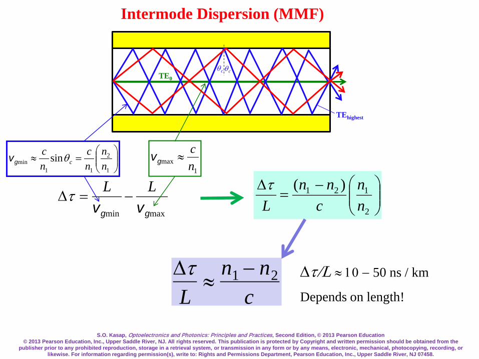
Intermode (Intermodal or Modal) Dispersion
Schematic illustration of light propagation in a slab dielectric waveguide. Light pulse entering the waveguide breaks up into various modes which
then propagate at different group velocities down the guide. At the end of the guide, the modes combine to constitute the output light pulse which is
broader than the input light pulse.

S.O. Kasap, Optoelectronics and Photonics: Principles and Practices, Second Edition, © 2013 Pearson Education© 2013 Pearson Education, Inc., Upper Saddle River, NJ. All rights reserved. This publication is protected by Copyright and written permission should be obtained from the
publisher prior to any prohibited reproduction, storage in a retrieval system, or transmission in any form or by any means, electronic, mechanical, photocopying, recording, or likewise. For information regarding permission(s), write to: Rights and Permissions Department, Pearson Education, Inc., Upper Saddle River, NJ 07458.
TE and TM Modes
Possible modes can be classified in terms of (a) transverse electric field (TE) and (b) transverse magnetic field (TM). Plane of incidence is the
paper.
B⊥ is along − x, so that B⊥ = −BxE⊥ is along x, so that E⊥ = Ex

S.O. Kasap, Optoelectronics and Photonics: Principles and Practices, Second Edition, © 2013 Pearson Education© 2013 Pearson Education, Inc., Upper Saddle River, NJ. All rights reserved. This publication is protected by Copyright and written permission should be obtained from the
publisher prior to any prohibited reproduction, storage in a retrieval system, or transmission in any form or by any means, electronic, mechanical, photocopying, recording, or likewise. For information regarding permission(s), write to: Rights and Permissions Department, Pearson Education, Inc., Upper Saddle River, NJ 07458.
V-NumberAll waveguides are characterized by a parameter called
the V-number or normalized frequency
V =2πaλ
n12 − n2
2( )1/ 2
V < π/2, m = 0 is the only possibility and only the fundamental mode (m = 0) propagates along the dielectric
slab waveguide: a single mode planar waveguide.
λ = λc for V = π/2 is the cut-off wavelength, and above this wavelength, only one-mode, the fundamental mode
will propagate.

S.O. Kasap, Optoelectronics and Photonics: Principles and Practices, Second Edition, © 2013 Pearson Education© 2013 Pearson Education, Inc., Upper Saddle River, NJ. All rights reserved. This publication is protected by Copyright and written permission should be obtained from the
publisher prior to any prohibited reproduction, storage in a retrieval system, or transmission in any form or by any means, electronic, mechanical, photocopying, recording, or likewise. For information regarding permission(s), write to: Rights and Permissions Department, Pearson Education, Inc., Upper Saddle River, NJ 07458.
Example on Waveguide ModesConsider a planar dielectric guide with a core thickness 20 µm, n1= 1.455, n2 = 1.440, light wavelength of 900 nm. Find the modes
( )m
m
m
nn
θ
θ
φcos
sin
tan
2/12
1
22
21
−
=
πφθλ
π manmm =−
cos)2(2 1Waveguide
condition
TIR phase change φm for
TE mode
Waveguidecondition
TE mode
πθφ mak mm −= cos2 1

S.O. Kasap, Optoelectronics and Photonics: Principles and Practices, Second Edition, © 2013 Pearson Education© 2013 Pearson Education, Inc., Upper Saddle River, NJ. All rights reserved. This publication is protected by Copyright and written permission should be obtained from the
publisher prior to any prohibited reproduction, storage in a retrieval system, or transmission in any form or by any means, electronic, mechanical, photocopying, recording, or likewise. For information regarding permission(s), write to: Rights and Permissions Department, Pearson Education, Inc., Upper Saddle River, NJ 07458.
)(cos
sin
2costan
2/12
1
22
1 mm
m
m fnn
mak θθ
θπθ =
−
=
−
TE mode

S.O. Kasap, Optoelectronics and Photonics: Principles and Practices, Second Edition, © 2013 Pearson Education© 2013 Pearson Education, Inc., Upper Saddle River, NJ. All rights reserved. This publication is protected by Copyright and written permission should be obtained from the
publisher prior to any prohibited reproduction, storage in a retrieval system, or transmission in any form or by any means, electronic, mechanical, photocopying, recording, or likewise. For information regarding permission(s), write to: Rights and Permissions Department, Pearson Education, Inc., Upper Saddle River, NJ 07458.
m 0 1 2 3 4 5 6 7 8 9
θm 89.2° 88.3° 87.5° 86.7° 85.9° 85.0° 84.2° 83.4° 82.6° 81.9°
δm (µm) 0.691 0.702 0.722 0.751 0.793 0.866 0.970 1.15 1.57 3.83
Critical angle θc = arcsin(n2/n1) = 81.77°
Highestmode
m = 0Fundamental
mode
λ
θπ
αδ
2/1
22
2
12 1sin2
1
−
==m
mm
nnn
Mode m, incidence angle θm and penetration δm for a planar dielectric waveguide with d = 2a = 20 µm, n1 = 1.455, n2 = 1.440 (λ = 900 nm)

S.O. Kasap, Optoelectronics and Photonics: Principles and Practices, Second Edition, © 2013 Pearson Education© 2013 Pearson Education, Inc., Upper Saddle River, NJ. All rights reserved. This publication is protected by Copyright and written permission should be obtained from the
publisher prior to any prohibited reproduction, storage in a retrieval system, or transmission in any form or by any means, electronic, mechanical, photocopying, recording, or likewise. For information regarding permission(s), write to: Rights and Permissions Department, Pearson Education, Inc., Upper Saddle River, NJ 07458.
Number of Modes M
2πn1(2a)λ
cosθm −φm = mπWaveguide
condition
1)2(Int +=πVM
One mode when V < π/2
Multimode when V > π/2

S.O. Kasap, Optoelectronics and Photonics: Principles and Practices, Second Edition, © 2013 Pearson Education© 2013 Pearson Education, Inc., Upper Saddle River, NJ. All rights reserved. This publication is protected by Copyright and written permission should be obtained from the
publisher prior to any prohibited reproduction, storage in a retrieval system, or transmission in any form or by any means, electronic, mechanical, photocopying, recording, or likewise. For information regarding permission(s), write to: Rights and Permissions Department, Pearson Education, Inc., Upper Saddle River, NJ 07458.
Mode Field Width 2woEcladding(y′) = Ecladding(0)exp(−αcladdingy′)
aVnn
nnn
i
=−≈
−
=
2/122
21
2/1
22
2
12cladding
)(2
1sin2
λπ
θλπα
∴ VVawo
)1(22 +≈
Mode Field Width 2wo
Note: The MFW definition here is semiquantitive. A more rigorous approach needs toconsider the optical power in the mode and how much of this penetrates the cladding. Seeoptical fibers section.

S.O. Kasap, Optoelectronics and Photonics: Principles and Practices, Second Edition, © 2013 Pearson Education© 2013 Pearson Education, Inc., Upper Saddle River, NJ. All rights reserved. This publication is protected by Copyright and written permission should be obtained from the
publisher prior to any prohibited reproduction, storage in a retrieval system, or transmission in any form or by any means, electronic, mechanical, photocopying, recording, or likewise. For information regarding permission(s), write to: Rights and Permissions Department, Pearson Education, Inc., Upper Saddle River, NJ 07458.
The slope of ω vs. β is the group velocity vg
Waveguide Dispersion Curve
gv=0β
ωdd
Slope = Group Velocity
βm
ω

S.O. Kasap, Optoelectronics and Photonics: Principles and Practices, Second Edition, © 2013 Pearson Education© 2013 Pearson Education, Inc., Upper Saddle River, NJ. All rights reserved. This publication is protected by Copyright and written permission should be obtained from the
publisher prior to any prohibited reproduction, storage in a retrieval system, or transmission in any form or by any means, electronic, mechanical, photocopying, recording, or likewise. For information regarding permission(s), write to: Rights and Permissions Department, Pearson Education, Inc., Upper Saddle River, NJ 07458.
Mode Group Velocities from Dispersion Diagram
The group velocity vg vs. ω for a planar dielectric guide with a core thickness (2a) = 20 µm, n1 = 1.455, n2 = 1.440. TE0, TE1 and TE4
Group velocity vs. frequency or wavelength behavior is not obvious. For the first few modes, a higher mode can travel faster than the fundamental.

S.O. Kasap, Optoelectronics and Photonics: Principles and Practices, Second Edition, © 2013 Pearson Education© 2013 Pearson Education, Inc., Upper Saddle River, NJ. All rights reserved. This publication is protected by Copyright and written permission should be obtained from the
publisher prior to any prohibited reproduction, storage in a retrieval system, or transmission in any form or by any means, electronic, mechanical, photocopying, recording, or likewise. For information regarding permission(s), write to: Rights and Permissions Department, Pearson Education, Inc., Upper Saddle River, NJ 07458.
A Planar Dielectric Waveguide with Many Modes
The group velocity vg vs. ω for a planar dielectric guideCore thickness (2a) = 20 µm, n1 = 1.455, n2 = 1.440
[Calculations by the author]
ω
vg
0.5×10¹⁶ 1.0×10¹⁶ 1.5×10160
2.04
2.05
2.06
2.07
2.08
×108
c / n2
c / n1
(c/n1)sinθc = cn2/n12
m = 0
m = 10
m = 20 m = 30 m = 40 m = 60ΤΕ1 ωcutoff
Slower than fundamental
Not in the textbook

S.O. Kasap, Optoelectronics and Photonics: Principles and Practices, Second Edition, © 2013 Pearson Education© 2013 Pearson Education, Inc., Upper Saddle River, NJ. All rights reserved. This publication is protected by Copyright and written permission should be obtained from the
publisher prior to any prohibited reproduction, storage in a retrieval system, or transmission in any form or by any means, electronic, mechanical, photocopying, recording, or likewise. For information regarding permission(s), write to: Rights and Permissions Department, Pearson Education, Inc., Upper Saddle River, NJ 07458.
Dispersion in the Planar Dielectric Waveguide with TE0 and TE1(Near cut-off)
TE0
TE1
=Broadened pulse
Output light pulse
Inputlightpulse
ω
vg
ωcutoff
c / n2
c / n1
Operatingfrequency
ω1
vgmax
vgmin
vgmax ≈ c/n2
vgmin ≈ c/n1
Spread in arrival times
Dispersion
TE1
TE0
TE2
ω1 ω1
λ1 = 2πc/ω1
Not in the textbook

S.O. Kasap, Optoelectronics and Photonics: Principles and Practices, Second Edition, © 2013 Pearson Education© 2013 Pearson Education, Inc., Upper Saddle River, NJ. All rights reserved. This publication is protected by Copyright and written permission should be obtained from the
publisher prior to any prohibited reproduction, storage in a retrieval system, or transmission in any form or by any means, electronic, mechanical, photocopying, recording, or likewise. For information regarding permission(s), write to: Rights and Permissions Department, Pearson Education, Inc., Upper Saddle River, NJ 07458.
A Planar Dielectric Waveguide with Many Modes
Multimode operation in which many modes propagate with different group velocities
vg vs. ω for a planar dielectric guide with a core thickness (2a) = 20 µm, n1 = 1.455, n2 = 1.440[Calculations by the author]
ω
vg
0.5×10¹⁶ 1.0×10¹⁶ 1.5×10160
2.04
2.05
2.06
2.07
2.08
×108
c / n2
c / n1
(c/n1)sinθc = cn2/n12
m = 0m = 25m = 35m = 45m = 55m = 65
ωcutoff
Operatingfrequency
Range of groupvelocities for 65 modes
Not in the textbook

S.O. Kasap, Optoelectronics and Photonics: Principles and Practices, Second Edition, © 2013 Pearson Education© 2013 Pearson Education, Inc., Upper Saddle River, NJ. All rights reserved. This publication is protected by Copyright and written permission should be obtained from the
publisher prior to any prohibited reproduction, storage in a retrieval system, or transmission in any form or by any means, electronic, mechanical, photocopying, recording, or likewise. For information regarding permission(s), write to: Rights and Permissions Department, Pearson Education, Inc., Upper Saddle River, NJ 07458.
Dispersion in the Planar Dielectric Waveguide with Many ModesFar from Cutoff
TEhighest
θc θcc/n1
(c/n1)sinθc c/n1
=≈
1
2
11min sin
nn
nc
nc
cθgv1
max nc
≈gv
maxmin
11gg vv
−=∆Lτ
cnn
nnnn
ccn
cnn
L)()(1 21
2
1211
2
21 −
≈
−=−=
∆τ
∆τL
≈n1 − n2
c(Since n1 and n2 are only slightly different.)
ω
vg
c / n1
(c/n1)sinθc
Operatingfrequency
Range of groupvelocities for 65 modes
c / n2
Not in the textbook

S.O. Kasap, Optoelectronics and Photonics: Principles and Practices, Second Edition, © 2013 Pearson Education© 2013 Pearson Education, Inc., Upper Saddle River, NJ. All rights reserved. This publication is protected by Copyright and written permission should be obtained from the
publisher prior to any prohibited reproduction, storage in a retrieval system, or transmission in any form or by any means, electronic, mechanical, photocopying, recording, or likewise. For information regarding permission(s), write to: Rights and Permissions Department, Pearson Education, Inc., Upper Saddle River, NJ 07458.
TEhighest
θc
Dispersion in the Planar Dielectric WaveguideMany Modes
=Broadened
pulseOutputpulse
Very short inputpulse
ω2
ω2
θcTE0
maxmin
11gg vv
−=∆Lτ
−≈
∆
2
121 )(nn
cnn
Lτ
∆τL
≈n1 − n2
c
∆τ
Not in the textbook
(Since n1/n2 ≈ 1)

S.O. Kasap, Optoelectronics and Photonics: Principles and Practices, Second Edition, © 2013 Pearson Education© 2013 Pearson Education, Inc., Upper Saddle River, NJ. All rights reserved. This publication is protected by Copyright and written permission should be obtained from the
publisher prior to any prohibited reproduction, storage in a retrieval system, or transmission in any form or by any means, electronic, mechanical, photocopying, recording, or likewise. For information regarding permission(s), write to: Rights and Permissions Department, Pearson Education, Inc., Upper Saddle River, NJ 07458.
How can a higher mode such as TE1 or TE2travel faster than the fundamental near cut-off?
Not in the textbook
The mode TE1 penetrates into the cladding where its velocity is higher than in the core. If penetration is large, as near cut-off, TE1
group velocity along the guide can exceed that of TE0.
θc
Pene
tratio
n de
pth
δ m
Incidence angle θi
TE1 near cut-off
Fundamental mode

S.O. Kasap, Optoelectronics and Photonics: Principles and Practices, Second Edition, © 2013 Pearson Education© 2013 Pearson Education, Inc., Upper Saddle River, NJ. All rights reserved. This publication is protected by Copyright and written permission should be obtained from the
publisher prior to any prohibited reproduction, storage in a retrieval system, or transmission in any form or by any means, electronic, mechanical, photocopying, recording, or likewise. For information regarding permission(s), write to: Rights and Permissions Department, Pearson Education, Inc., Upper Saddle River, NJ 07458.
The electric field of TE0 mode extends more into the cladding as the wavelength increases. As more of the field is carried by the cladding, the group
velocity increases.
Group Velocity and Wavelength: Fundamental Mode

S.O. Kasap, Optoelectronics and Photonics: Principles and Practices, Second Edition, © 2013 Pearson Education© 2013 Pearson Education, Inc., Upper Saddle River, NJ. All rights reserved. This publication is protected by Copyright and written permission should be obtained from the
publisher prior to any prohibited reproduction, storage in a retrieval system, or transmission in any form or by any means, electronic, mechanical, photocopying, recording, or likewise. For information regarding permission(s), write to: Rights and Permissions Department, Pearson Education, Inc., Upper Saddle River, NJ 07458.
Optical Fibers
The step index optical fiber. The central region, the core, has greater refractive index than the outer region, the cladding. The fiber has cylindrical
symmetry. The coordinates r, φ, z are used to represent any point P in the fiber. Cladding is normally much thicker than shown.

S.O. Kasap, Optoelectronics and Photonics: Principles and Practices, Second Edition, © 2013 Pearson Education© 2013 Pearson Education, Inc., Upper Saddle River, NJ. All rights reserved. This publication is protected by Copyright and written permission should be obtained from the
publisher prior to any prohibited reproduction, storage in a retrieval system, or transmission in any form or by any means, electronic, mechanical, photocopying, recording, or likewise. For information regarding permission(s), write to: Rights and Permissions Department, Pearson Education, Inc., Upper Saddle River, NJ 07458.
Meridional ray enters the fiber through the fiber axis and hence also crosses the fiber axis on each reflection as it zigzags down the fiber. It travels in a plane that contains the fiber axis.
Skew ray enters the fiber off the fiber axis and zigzags down the fiber without crossing the axis

S.O. Kasap, Optoelectronics and Photonics: Principles and Practices, Second Edition, © 2013 Pearson Education© 2013 Pearson Education, Inc., Upper Saddle River, NJ. All rights reserved. This publication is protected by Copyright and written permission should be obtained from the
publisher prior to any prohibited reproduction, storage in a retrieval system, or transmission in any form or by any means, electronic, mechanical, photocopying, recording, or likewise. For information regarding permission(s), write to: Rights and Permissions Department, Pearson Education, Inc., Upper Saddle River, NJ 07458.
Modes LPlm
Weakly guiding modes in fibers
∆ << 1 weakly guiding fibers
ELP = Elm(r,φ) expj(ωt − βlmz)
Traveling wave
FieldPattern
E and B are 90o to each other and z

S.O. Kasap, Optoelectronics and Photonics: Principles and Practices, Second Edition, © 2013 Pearson Education© 2013 Pearson Education, Inc., Upper Saddle River, NJ. All rights reserved. This publication is protected by Copyright and written permission should be obtained from the
publisher prior to any prohibited reproduction, storage in a retrieval system, or transmission in any form or by any means, electronic, mechanical, photocopying, recording, or likewise. For information regarding permission(s), write to: Rights and Permissions Department, Pearson Education, Inc., Upper Saddle River, NJ 07458.
Fundamental Mode is the LP01 mode: l = 0 and m = 1
The electric field distribution of the fundamental mode, LP01, in the
transverse plane to the fiber axis z. The light intensity is greatest at the center of
the fiber

S.O. Kasap, Optoelectronics and Photonics: Principles and Practices, Second Edition, © 2013 Pearson Education© 2013 Pearson Education, Inc., Upper Saddle River, NJ. All rights reserved. This publication is protected by Copyright and written permission should be obtained from the
publisher prior to any prohibited reproduction, storage in a retrieval system, or transmission in any form or by any means, electronic, mechanical, photocopying, recording, or likewise. For information regarding permission(s), write to: Rights and Permissions Department, Pearson Education, Inc., Upper Saddle River, NJ 07458.
The electric field distribution of the fundamental mode in the transverse plane to the fiber axis z. The light intensity is greatest at the center of the fiber. Intensity patterns in LP01, LP11 and LP21 modes. (a) The field in the fundamental mode. (b)-(d) Indicative
light intensity distributions in three modes, LP01, LP11 and LP21.

S.O. Kasap, Optoelectronics and Photonics: Principles and Practices, Second Edition, © 2013 Pearson Education© 2013 Pearson Education, Inc., Upper Saddle River, NJ. All rights reserved. This publication is protected by Copyright and written permission should be obtained from the
publisher prior to any prohibited reproduction, storage in a retrieval system, or transmission in any form or by any means, electronic, mechanical, photocopying, recording, or likewise. For information regarding permission(s), write to: Rights and Permissions Department, Pearson Education, Inc., Upper Saddle River, NJ 07458.
LPlm
m = number of maxima along r starting from the core center. Determines the reflection angle θ
2l = number of maxima around a circumference
l - radial mode numberl - extent of helical propagation, i.e. the amount of skew ray contribution to the mode.
ELP = Elm(r,φ) expj(ωt − βlmz)

S.O. Kasap, Optoelectronics and Photonics: Principles and Practices, Second Edition, © 2013 Pearson Education© 2013 Pearson Education, Inc., Upper Saddle River, NJ. All rights reserved. This publication is protected by Copyright and written permission should be obtained from the
publisher prior to any prohibited reproduction, storage in a retrieval system, or transmission in any form or by any means, electronic, mechanical, photocopying, recording, or likewise. For information regarding permission(s), write to: Rights and Permissions Department, Pearson Education, Inc., Upper Saddle River, NJ 07458.
Optical Fiber Parameters
n = (n1 + n2)/2 = average refractive index∆ = normalized index difference∆ = (n1 − n2)/n1 ≈ (n1
2 − n22)/2
V =2πaλ
n12 − n2
2( )1/ 2=
2πaλ
2n1n∆( )1/ 2V-number
V < 2.405 only 1 mode exists. Fundamental mode
V < 2.405 or λ > λc Single mode fiber
V > 2.405 Multimode fiber
Number of modes 2
2VM ≈

S.O. Kasap, Optoelectronics and Photonics: Principles and Practices, Second Edition, © 2013 Pearson Education© 2013 Pearson Education, Inc., Upper Saddle River, NJ. All rights reserved. This publication is protected by Copyright and written permission should be obtained from the
publisher prior to any prohibited reproduction, storage in a retrieval system, or transmission in any form or by any means, electronic, mechanical, photocopying, recording, or likewise. For information regarding permission(s), write to: Rights and Permissions Department, Pearson Education, Inc., Upper Saddle River, NJ 07458.
b =(β /k)2 − n2
2
n12 − n2
2
Modes in an Optical Fiber
Normalized propagation constant
k = 2π/λ
2996.01428.1
−≈
Vb
Normalized propagation constant b vs. V-number for a step-index fiber for various LP modes
( 1.5 < V < 2.5)

S.O. Kasap, Optoelectronics and Photonics: Principles and Practices, Second Edition, © 2013 Pearson Education© 2013 Pearson Education, Inc., Upper Saddle River, NJ. All rights reserved. This publication is protected by Copyright and written permission should be obtained from the
publisher prior to any prohibited reproduction, storage in a retrieval system, or transmission in any form or by any means, electronic, mechanical, photocopying, recording, or likewise. For information regarding permission(s), write to: Rights and Permissions Department, Pearson Education, Inc., Upper Saddle River, NJ 07458.
Group Velocity and Group Delay
Consider a single mode fiber with core and cladding indices of 1.4480 and 1.4400, core radius of 3 µm, operating at 1.5 µm. What are the group velocity and group delay at this wavelength?
b ≈ 1.1428 −0.996
V
2
1.5 < V < 2.5
b =(β / k) − n2
n1 − n2
β = n2k[1 + b∆]
k = 2π/λ = 4,188,790 m-1 and ω = 2πc/λ = 1.255757×10¹⁵ rad s-1
V = (2πa/λ)(n12 − n2
2 )1/2 = 1.910088
b = 0.3860859, and β = 6.044796×10⁶ m-1.
Increase wavelength by 0.1% and recalculate. Values in the table

S.O. Kasap, Optoelectronics and Photonics: Principles and Practices, Second Edition, © 2013 Pearson Education© 2013 Pearson Education, Inc., Upper Saddle River, NJ. All rights reserved. This publication is protected by Copyright and written permission should be obtained from the
publisher prior to any prohibited reproduction, storage in a retrieval system, or transmission in any form or by any means, electronic, mechanical, photocopying, recording, or likewise. For information regarding permission(s), write to: Rights and Permissions Department, Pearson Education, Inc., Upper Saddle River, NJ 07458.
Group Velocity and Group Delay
The group delay τg over 1 km is 4.83 µs
Calculation → V k (m-1) ω (rad s-1) b β (m-1)
λ = 1.500000 µm 1.910088 4188790 1.255757×10¹⁵ 0.3860859 6.044818×10⁶
λ′ = 1.50150 µm 1.908180 4184606 1.254503×10¹⁵ 0.3854382 6.038757×10⁶
186
15
sm1007.210)044818.6038757.6(10)255757.1254503.1( −×≈
×−×−
=−′−′
==ββωω
βω
dd
gv

S.O. Kasap, Optoelectronics and Photonics: Principles and Practices, Second Edition, © 2013 Pearson Education© 2013 Pearson Education, Inc., Upper Saddle River, NJ. All rights reserved. This publication is protected by Copyright and written permission should be obtained from the
publisher prior to any prohibited reproduction, storage in a retrieval system, or transmission in any form or by any means, electronic, mechanical, photocopying, recording, or likewise. For information regarding permission(s), write to: Rights and Permissions Department, Pearson Education, Inc., Upper Saddle River, NJ 07458.
Mode Field Diameter (2w)
])/(exp[)0()( 2wrErE −= ])/(2exp[)0()( 222 wrErE −=
Gaussian Gaussian
Intensity ∝ vg×E(r)2
Note: Maximum set
arbitrarily to 1

S.O. Kasap, Optoelectronics and Photonics: Principles and Practices, Second Edition, © 2013 Pearson Education© 2013 Pearson Education, Inc., Upper Saddle River, NJ. All rights reserved. This publication is protected by Copyright and written permission should be obtained from the
publisher prior to any prohibited reproduction, storage in a retrieval system, or transmission in any form or by any means, electronic, mechanical, photocopying, recording, or likewise. For information regarding permission(s), write to: Rights and Permissions Department, Pearson Education, Inc., Upper Saddle River, NJ 07458.
Mode Field Diameter
)879.2619.165.0(22 62/3 −− ++= VVaw 0.8 < V < 2.5
2w ≈ (2a)(2.6V) 1.6 < V < 2.4
Marcuse MFD Equation
])/(2exp[)0()( 222 wrErE −=
Intensity ∝ vg×E(r)2Note:
Maximum set arbitrarily to 1
2w = Mode Field Diameter (MFD)

S.O. Kasap, Optoelectronics and Photonics: Principles and Practices, Second Edition, © 2013 Pearson Education© 2013 Pearson Education, Inc., Upper Saddle River, NJ. All rights reserved. This publication is protected by Copyright and written permission should be obtained from the
publisher prior to any prohibited reproduction, storage in a retrieval system, or transmission in any form or by any means, electronic, mechanical, photocopying, recording, or likewise. For information regarding permission(s), write to: Rights and Permissions Department, Pearson Education, Inc., Upper Saddle River, NJ 07458.
Correction note p113
Applies to print version only; e-version is correct
])/(2exp[)0()( 222 wrErE −=
Insert this 2 in Equation (2.3.7)Insert this 2 as superscript on e
in Figure 2.16

S.O. Kasap, Optoelectronics and Photonics: Principles and Practices, Second Edition, © 2013 Pearson Education© 2013 Pearson Education, Inc., Upper Saddle River, NJ. All rights reserved. This publication is protected by Copyright and written permission should be obtained from the
publisher prior to any prohibited reproduction, storage in a retrieval system, or transmission in any form or by any means, electronic, mechanical, photocopying, recording, or likewise. For information regarding permission(s), write to: Rights and Permissions Department, Pearson Education, Inc., Upper Saddle River, NJ 07458.
])/(2exp[)0()( 222 wrErE −=
865.02)(
2)(
0
2
0
2
=
∫
∫∞
rdrrE
rdrrEw
π
πFraction of optical power
within MFD =
Area of a circular thin strip (annulus) with radius r is 2πrdr. Power passing through this strip is proportional to E(r)2(2πr)dr
Intensity ∝ vg×E(r)2and
Mode Field Diameter (2w)Not in the textbook

S.O. Kasap, Optoelectronics and Photonics: Principles and Practices, Second Edition, © 2013 Pearson Education© 2013 Pearson Education, Inc., Upper Saddle River, NJ. All rights reserved. This publication is protected by Copyright and written permission should be obtained from the
publisher prior to any prohibited reproduction, storage in a retrieval system, or transmission in any form or by any means, electronic, mechanical, photocopying, recording, or likewise. For information regarding permission(s), write to: Rights and Permissions Department, Pearson Education, Inc., Upper Saddle River, NJ 07458.
])/(2exp[)0()( 222 wrErE −=
86% of total power
Fraction of optical power within MFD = 86 %
This is the same as the fraction of optical power within a radius w from the axis of a Gaussian beam (See Chapter 1)
Mode Field Diameter (2w)

S.O. Kasap, Optoelectronics and Photonics: Principles and Practices, Second Edition, © 2013 Pearson Education© 2013 Pearson Education, Inc., Upper Saddle River, NJ. All rights reserved. This publication is protected by Copyright and written permission should be obtained from the
publisher prior to any prohibited reproduction, storage in a retrieval system, or transmission in any form or by any means, electronic, mechanical, photocopying, recording, or likewise. For information regarding permission(s), write to: Rights and Permissions Department, Pearson Education, Inc., Upper Saddle River, NJ 07458.
Example: A multimode fiberCalculate the number of allowed modes in a multimode step index fiber which has a core of refractive index of 1.468 and diameter 100 µm, and a cladding of refractive index of 1.447 if the source wavelength is 850 nm.SolutionSubstitute, a = 50 µm, λ = 0.850 µm, n1 = 1.468, n2 = 1.447 into the expression for the V-number, V = (2πa/λ)(n1
2 − n22)1/2 = (2π50/0.850)(1.4682 − 1.4472)1/2
= 91.44.Since V >> 2.405, the number of modes isM ≈ V2/2 = (91.44)2/2 = 4181which is large.

S.O. Kasap, Optoelectronics and Photonics: Principles and Practices, Second Edition, © 2013 Pearson Education© 2013 Pearson Education, Inc., Upper Saddle River, NJ. All rights reserved. This publication is protected by Copyright and written permission should be obtained from the
publisher prior to any prohibited reproduction, storage in a retrieval system, or transmission in any form or by any means, electronic, mechanical, photocopying, recording, or likewise. For information regarding permission(s), write to: Rights and Permissions Department, Pearson Education, Inc., Upper Saddle River, NJ 07458.
Example: A single mode fiberWhat should be the core radius of a single mode fiber which has a core of n1 = 1.4680, cladding of n2 = 1.447 and it is to be used with a source wavelength of 1.3 µm?SolutionFor single mode propagation, V ≤ 2.405. We need, V = (2πa/λ)(n1
2 − n22)1/2 ≤ 2.405
or[2πa/(1.3 µm)](1.4682 − 1.4472)1/2 ≤ 2.405 which gives a ≤ 2.01 µm. Rather thin for easy coupling of the fiber to a light source or to another fiber; a is comparable to λ which means that the geometric ray picture, strictly, cannot be used to describe light propagation.

S.O. Kasap, Optoelectronics and Photonics: Principles and Practices, Second Edition, © 2013 Pearson Education© 2013 Pearson Education, Inc., Upper Saddle River, NJ. All rights reserved. This publication is protected by Copyright and written permission should be obtained from the
publisher prior to any prohibited reproduction, storage in a retrieval system, or transmission in any form or by any means, electronic, mechanical, photocopying, recording, or likewise. For information regarding permission(s), write to: Rights and Permissions Department, Pearson Education, Inc., Upper Saddle River, NJ 07458.
Example: Single mode cut-off wavelengthCalculate the cut-off wavelength for single mode operation for a fiber that has a core with diameter of 8.2 µm, a refractive index of 1.4532, and a cladding of refractive index of 1.4485. What is the V-number and the mode field diameter (MFD) for operation at λ = 1.31 µm?
SolutionFor single mode operation, V = (2πa/λ)(n1
2 − n22 )1/2 ≤ 2.405
Substituting for a, n1 and n2 and rearranging we get,λ > [2π(4.1 µm)(1.45322 − 1.44852)1/2]/2.405 = 1.251 µmWavelengths shorter than 1.251 µm give multimode propagation.At λ = 1.31 µm,V = 2π[(4.1 µm)/(1.31 µm)](1.45322 − 1.44852)1/2 = 2.30 Mode field diameter MFD

S.O. Kasap, Optoelectronics and Photonics: Principles and Practices, Second Edition, © 2013 Pearson Education© 2013 Pearson Education, Inc., Upper Saddle River, NJ. All rights reserved. This publication is protected by Copyright and written permission should be obtained from the
publisher prior to any prohibited reproduction, storage in a retrieval system, or transmission in any form or by any means, electronic, mechanical, photocopying, recording, or likewise. For information regarding permission(s), write to: Rights and Permissions Department, Pearson Education, Inc., Upper Saddle River, NJ 07458.
Solution (continued)Mode field diameter MFD from the Marcuse Equation is
])30.2(88.2)30.2(62.165.0)[1.4(2)879.2619.165.0(22
62/3
62/3
−−
−−
++=
++= VVaw
2w = 9.30 µm
2w = (2a)(2.6/V) = 2(4.1)(2.6/2.30) = 9.28 µm
2w = 2a[(V+1)/V] = 11.8 µm This is for a planar waveguide, and the definition is different than that for an optical fiber
86% of total power is within this diameter

S.O. Kasap, Optoelectronics and Photonics: Principles and Practices, Second Edition, © 2013 Pearson Education© 2013 Pearson Education, Inc., Upper Saddle River, NJ. All rights reserved. This publication is protected by Copyright and written permission should be obtained from the
publisher prior to any prohibited reproduction, storage in a retrieval system, or transmission in any form or by any means, electronic, mechanical, photocopying, recording, or likewise. For information regarding permission(s), write to: Rights and Permissions Department, Pearson Education, Inc., Upper Saddle River, NJ 07458.
Numerical Aperture NA
( ) 2/122
21NA nn −=
( )oo nn
nn NAsin2/12
221 =
−=maxα
2αmax = total acceptance angle
NA is an important factor in light launching designs into the optical fiber.
Maximum acceptance angle αmax is that which just gives total internal reflection at the core-cladding interface, i.e. when α = αmax then θ = θc. Rays with α > αmax (e.g. ray B) become refracted and penetrate the cladding and are eventually lost.
NA2λπaV =
S.O. Kasap, Optoelectronics and Photonics: Principles and Practices, Second Edition, © 2013 Pearson Education© 2013 Pearson Education, Inc., Upper Saddle River, NJ. All rights reserved. This publication is protected by Copyright and written permission should be obtained from the
publisher prior to any prohibited reproduction, storage in a retrieval system, or transmission in any form or by any means, electronic, mechanical, photocopying, recording, or likewise. For information regarding permission(s), write to: Rights and Permissions Department, Pearson Education, Inc., Upper Saddle River, NJ 07458.
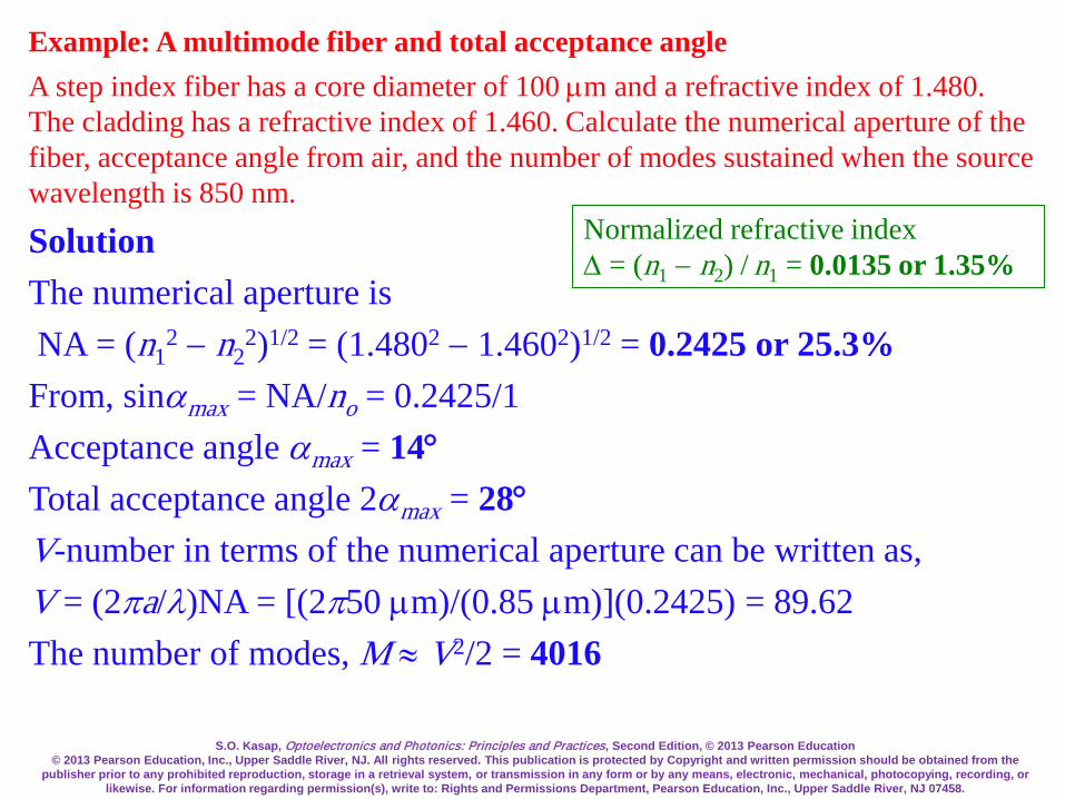
Example: A multimode fiber and total acceptance angleA step index fiber has a core diameter of 100 µm and a refractive index of 1.480. The cladding has a refractive index of 1.460. Calculate the numerical aperture of the fiber, acceptance angle from air, and the number of modes sustained when the source wavelength is 850 nm.
SolutionThe numerical aperture isNA = (n1
2 − n22)1/2 = (1.4802 − 1.4602)1/2 = 0.2425 or 25.3%
From, sinαmax = NA/no = 0.2425/1Acceptance angle αmax = 14°Total acceptance angle 2αmax = 28°V-number in terms of the numerical aperture can be written as, V = (2πa/λ)NA = [(2π50 µm)/(0.85 µm)](0.2425) = 89.62The number of modes, M ≈ V2/2 = 4016
Normalized refractive index∆ = (n1 − n2) / n1 = 0.0135 or 1.35%

S.O. Kasap, Optoelectronics and Photonics: Principles and Practices, Second Edition, © 2013 Pearson Education© 2013 Pearson Education, Inc., Upper Saddle River, NJ. All rights reserved. This publication is protected by Copyright and written permission should be obtained from the
publisher prior to any prohibited reproduction, storage in a retrieval system, or transmission in any form or by any means, electronic, mechanical, photocopying, recording, or likewise. For information regarding permission(s), write to: Rights and Permissions Department, Pearson Education, Inc., Upper Saddle River, NJ 07458.
Example: A single mode fiberA typical single mode optical fiber has a core of diameter 8 µm and a refractive index of 1.460. The normalized index difference is 0.3%. The cladding diameter is 125 µm. Calculate the numerical aperture and the total acceptance angle of the fiber. What is the single mode cut-off frequency λc of the fiber?SolutionThe numerical apertureNA = (n1
2 − n22)1/2 = [(n1 + n2)(n1 − n2)]1/2
Substituting (n1 − n2) = n1∆ and (n1 + n2) ≈ 2n1, we get NA ≈ [(2n1)(n1∆)]1/2 = n1(2∆)1/2 = 1.46(2×0.003)1/2 = 0.113 or 11.3 %The acceptance angle is given by sinαmax = NA/no = 0.113/1 or αmax = 6.5°, and 2αmax = 13°The condition for single mode propagation is V ≤ 2.405 which corresponds to a minimum wavelength λc is given by λc = [2πaNA]/2.405 = [(2π)(4 µm)(0.113)]/2.405 = 1.18 µmWavelengths shorter than 1.18 µm will result in multimode operation.

S.O. Kasap, Optoelectronics and Photonics: Principles and Practices, Second Edition, © 2013 Pearson Education© 2013 Pearson Education, Inc., Upper Saddle River, NJ. All rights reserved. This publication is protected by Copyright and written permission should be obtained from the
publisher prior to any prohibited reproduction, storage in a retrieval system, or transmission in any form or by any means, electronic, mechanical, photocopying, recording, or likewise. For information regarding permission(s), write to: Rights and Permissions Department, Pearson Education, Inc., Upper Saddle River, NJ 07458.
Dispersion = Spread of Information
• Intermode (Intermodal) Dispersion: Multimode fibers only
• Material DispersionGroup velocity depends on Ng and hence on λ
• Waveguide DispersionGroup velocity depends on waveguide structure
• Chromatic DispersionMaterial dispersion + Waveguide Dispersion
• Polarization Dispersion
• Profile DispersionLike material and waveguide dispersion. Add all 3Material + Waveguide + Profile
• Self phase modulation dispersion

S.O. Kasap, Optoelectronics and Photonics: Principles and Practices, Second Edition, © 2013 Pearson Education© 2013 Pearson Education, Inc., Upper Saddle River, NJ. All rights reserved. This publication is protected by Copyright and written permission should be obtained from the
publisher prior to any prohibited reproduction, storage in a retrieval system, or transmission in any form or by any means, electronic, mechanical, photocopying, recording, or likewise. For information regarding permission(s), write to: Rights and Permissions Department, Pearson Education, Inc., Upper Saddle River, NJ 07458.
Intermode Dispersion (MMF)
∆τL
≈n1 − n2
c
Group Delay τ = L / vg
(Since n1 and n2 are only slightly different)
S.O. Kasap, Optoelectronics and Photonics: Principles and Practices, Second Edition, © 2013 Pearson Education© 2013 Pearson Education, Inc., Upper Saddle River, NJ. All rights reserved. This publication is protected by Copyright and written permission should be obtained from the
publisher prior to any prohibited reproduction, storage in a retrieval system, or transmission in any form or by any means, electronic, mechanical, photocopying, recording, or likewise. For information regarding permission(s), write to: Rights and Permissions Department, Pearson Education, Inc., Upper Saddle River, NJ 07458.
Intermode Dispersion (MMF)
maxmin gg vvLL
−=∆τ
∆τL
≈n1 − n2
c∆τ/L ≈ 10 − 50 ns / km
Depends on length!
=≈
1
2
11min sin
nn
nc
nc
cθgv
−=
∆
2
121 )(nn
cnn
Lτ
θc θcTE0
TEhighest
1max n
c≈gv

S.O. Kasap, Optoelectronics and Photonics: Principles and Practices, Second Edition, © 2013 Pearson Education© 2013 Pearson Education, Inc., Upper Saddle River, NJ. All rights reserved. This publication is protected by Copyright and written permission should be obtained from the
publisher prior to any prohibited reproduction, storage in a retrieval system, or transmission in any form or by any means, electronic, mechanical, photocopying, recording, or likewise. For information regarding permission(s), write to: Rights and Permissions Department, Pearson Education, Inc., Upper Saddle River, NJ 07458.
Intramode Dispersion (SMF)
Group Delay τ = L / vg
Group velocity vg depends onRefractive index = n(λ) Material DispersionV-number = V(λ) Waveguide Dispersion∆ = (n1 − n2)/n1 = ∆(λ) Profile Dispersion
Dispersion in the fundamental mode

S.O. Kasap, Optoelectronics and Photonics: Principles and Practices, Second Edition, © 2013 Pearson Education© 2013 Pearson Education, Inc., Upper Saddle River, NJ. All rights reserved. This publication is protected by Copyright and written permission should be obtained from the
publisher prior to any prohibited reproduction, storage in a retrieval system, or transmission in any form or by any means, electronic, mechanical, photocopying, recording, or likewise. For information regarding permission(s), write to: Rights and Permissions Department, Pearson Education, Inc., Upper Saddle River, NJ 07458.
Intramode Dispersion (SMF)Chromatic dispersion in the fundamental mode
λ1
vg1vg2
∆λ = λ2 − λ1
λ2 τg1 τg2
τ
∆λ
δ(t)
∆τ
∆τ = τg1 − τg2
λτ
LddD =
DispersionChromatic spread
Definition of Dispersion Coefficient
λτ
∆∆
=L
D
OR
λτ ∆=∆ DLOutput pulse
dispersed

S.O. Kasap, Optoelectronics and Photonics: Principles and Practices, Second Edition, © 2013 Pearson Education© 2013 Pearson Education, Inc., Upper Saddle River, NJ. All rights reserved. This publication is protected by Copyright and written permission should be obtained from the
publisher prior to any prohibited reproduction, storage in a retrieval system, or transmission in any form or by any means, electronic, mechanical, photocopying, recording, or likewise. For information regarding permission(s), write to: Rights and Permissions Department, Pearson Education, Inc., Upper Saddle River, NJ 07458.
Material Dispersion
Emitter emits a spectrum ∆λ of wavelengths.
Waves in the guide with different free space wavelengths travel at different groupvelocities due to the wavelength dependence of n1. The waves arrive at the end of thefiber at different times and hence result in a broadened output pulse.
∆τL
= Dm∆λ Dm = Material dispersion coefficient, ps nm-1 km-1

S.O. Kasap, Optoelectronics and Photonics: Principles and Practices, Second Edition, © 2013 Pearson Education© 2013 Pearson Education, Inc., Upper Saddle River, NJ. All rights reserved. This publication is protected by Copyright and written permission should be obtained from the
publisher prior to any prohibited reproduction, storage in a retrieval system, or transmission in any form or by any means, electronic, mechanical, photocopying, recording, or likewise. For information regarding permission(s), write to: Rights and Permissions Department, Pearson Education, Inc., Upper Saddle River, NJ 07458.
Material Dispersion
∆τL
= Dm∆λ
Dm = Material dispersion coefficient, ps nm-1 km-1
Cladding
CoreEmitter
Very shortlight pulse
vg(λ1)Input
Outputvg(λ2)
vg = c / NgDepends on the wavelengthGroup velocity
−≈ 2
2
λλ
dnd
cDm

S.O. Kasap, Optoelectronics and Photonics: Principles and Practices, Second Edition, © 2013 Pearson Education© 2013 Pearson Education, Inc., Upper Saddle River, NJ. All rights reserved. This publication is protected by Copyright and written permission should be obtained from the
publisher prior to any prohibited reproduction, storage in a retrieval system, or transmission in any form or by any means, electronic, mechanical, photocopying, recording, or likewise. For information regarding permission(s), write to: Rights and Permissions Department, Pearson Education, Inc., Upper Saddle River, NJ 07458.
b =(β /k)2 − n2
2
n12 − n2
2
Wave guide dispersion
b hence β depend on V and hence on λ
Normalized propagation constant
k = 2π/λ
2996.01428.1
−≈
Vb( ) 2/12
221
2 nnaV −=λπ

S.O. Kasap, Optoelectronics and Photonics: Principles and Practices, Second Edition, © 2013 Pearson Education© 2013 Pearson Education, Inc., Upper Saddle River, NJ. All rights reserved. This publication is protected by Copyright and written permission should be obtained from the
publisher prior to any prohibited reproduction, storage in a retrieval system, or transmission in any form or by any means, electronic, mechanical, photocopying, recording, or likewise. For information regarding permission(s), write to: Rights and Permissions Department, Pearson Education, Inc., Upper Saddle River, NJ 07458.
Waveguide Dispersion
Waveguide dispersion The group velocity vg(01) of the fundamental mode depends on the V-number, which itself depends on the source wavelength λ, even if n1 and n2 were constant. Even if n1 and n2 were wavelength independent (no material dispersion), we will still have waveguide dispersion by virtue of vg(01) depending on V and Vdepending inversely on λ. Waveguide dispersion arises as a result of the guiding properties of the waveguide which imposes a nonlinear ω vs. βlm relationship.
∆τL
= Dw∆λDw = waveguide dispersion coefficient
Dw depends on the waveguide structure, ps nm-1 km-1

S.O. Kasap, Optoelectronics and Photonics: Principles and Practices, Second Edition, © 2013 Pearson Education© 2013 Pearson Education, Inc., Upper Saddle River, NJ. All rights reserved. This publication is protected by Copyright and written permission should be obtained from the
publisher prior to any prohibited reproduction, storage in a retrieval system, or transmission in any form or by any means, electronic, mechanical, photocopying, recording, or likewise. For information regarding permission(s), write to: Rights and Permissions Department, Pearson Education, Inc., Upper Saddle River, NJ 07458.
Chromatic Dispersion
Material dispersion coefficient (Dm) for the core material (taken as SiO2), waveguide dispersion coefficient (Dw) (a = 4.2 µm) and the total or chromatic dispersion coefficient Dch (= Dm + Dw) as a function of free space wavelength, λ
∆τL
= (Dm + Dw)∆λ
Chromatic = Material + Waveguide

S.O. Kasap, Optoelectronics and Photonics: Principles and Practices, Second Edition, © 2013 Pearson Education© 2013 Pearson Education, Inc., Upper Saddle River, NJ. All rights reserved. This publication is protected by Copyright and written permission should be obtained from the
publisher prior to any prohibited reproduction, storage in a retrieval system, or transmission in any form or by any means, electronic, mechanical, photocopying, recording, or likewise. For information regarding permission(s), write to: Rights and Permissions Department, Pearson Education, Inc., Upper Saddle River, NJ 07458.
What do Negative and Positive Dm mean?
λ1
12
λ2
t
λ1 vg1vg2λ2
t
∆λ = λ2 − λ1
1 2
λ1 λ2
Positive Dm
Ng2 > Ng1
∆τ = Positive
t
λ1 vg1
vg2λ2t
Negative Dm
Ng2 < Ng1
∆τ = Negative
Negative DmPositive Dm
Dm
λτ
∆∆
=L
Dm
Silica glass ∆τ

S.O. Kasap, Optoelectronics and Photonics: Principles and Practices, Second Edition, © 2013 Pearson Education© 2013 Pearson Education, Inc., Upper Saddle River, NJ. All rights reserved. This publication is protected by Copyright and written permission should be obtained from the
publisher prior to any prohibited reproduction, storage in a retrieval system, or transmission in any form or by any means, electronic, mechanical, photocopying, recording, or likewise. For information regarding permission(s), write to: Rights and Permissions Department, Pearson Education, Inc., Upper Saddle River, NJ 07458.
∆= 2
22 )(
dVbVdV
cnDw λ
Waveguide Dimension and Chromatic Dispersion
22025.0cna
Dwλ
−≈
22
11
)]μm([)μm(76.83)kmnmps(
naDw
λ−≈−−
Waveguide dispersion depends on the guide properties

S.O. Kasap, Optoelectronics and Photonics: Principles and Practices, Second Edition, © 2013 Pearson Education© 2013 Pearson Education, Inc., Upper Saddle River, NJ. All rights reserved. This publication is protected by Copyright and written permission should be obtained from the
publisher prior to any prohibited reproduction, storage in a retrieval system, or transmission in any form or by any means, electronic, mechanical, photocopying, recording, or likewise. For information regarding permission(s), write to: Rights and Permissions Department, Pearson Education, Inc., Upper Saddle River, NJ 07458.
Profile Dispersion
Group velocity vg(01) of the fundamental mode depends on ∆, refractive index difference.
∆ may not be constant over a range of wavelengths: ∆ = ∆(λ)
∆τL
= Dp∆λ Dp = Profile dispersion coefficient
Dp < 0.1 ps nm-1 km-1
Can generally be ignored
NOTETotal intramode (chromatic) dispersion coefficient Dch
Dch = Dm + Dw + Dp
where Dm, Dw, Dp are material, waveguide and profile dispersion coefficients respectively

S.O. Kasap, Optoelectronics and Photonics: Principles and Practices, Second Edition, © 2013 Pearson Education© 2013 Pearson Education, Inc., Upper Saddle River, NJ. All rights reserved. This publication is protected by Copyright and written permission should be obtained from the
publisher prior to any prohibited reproduction, storage in a retrieval system, or transmission in any form or by any means, electronic, mechanical, photocopying, recording, or likewise. For information regarding permission(s), write to: Rights and Permissions Department, Pearson Education, Inc., Upper Saddle River, NJ 07458.
Chromatic Dispersion
λτ∆=
∆chD
L
−=
400 1
4 λλλSDch
Dch = Dm + Dw + Dp
S0 = Chromatic dispersion slope at λ0
Chromatic dispersion is zero at λ = λ0

S.O. Kasap, Optoelectronics and Photonics: Principles and Practices, Second Edition, © 2013 Pearson Education© 2013 Pearson Education, Inc., Upper Saddle River, NJ. All rights reserved. This publication is protected by Copyright and written permission should be obtained from the
publisher prior to any prohibited reproduction, storage in a retrieval system, or transmission in any form or by any means, electronic, mechanical, photocopying, recording, or likewise. For information regarding permission(s), write to: Rights and Permissions Department, Pearson Education, Inc., Upper Saddle River, NJ 07458.
+∆
+∆
=−=∆ 2
2
2
0 )(!2
1)()()(00
λλτλ
λτλτλττ
λλ dd
dd
Is dispersion really zero at λ0?The cause of ∆τ is the wavelength
spread ∆λ at the input∆τ = f(∆λ)
chDLdd
=∆
λτ
( )( ) ps01.1nm2kmnmps090.02km1)(
221-2-2
0 ==∆=∆ λτ SL
0Sd
dDch =λ
20 )(
21)]([
0
λλτ
λλλτ
λ
∆
+∆=∆
dd
ddLDch
= 0

S.O. Kasap, Optoelectronics and Photonics: Principles and Practices, Second Edition, © 2013 Pearson Education© 2013 Pearson Education, Inc., Upper Saddle River, NJ. All rights reserved. This publication is protected by Copyright and written permission should be obtained from the
publisher prior to any prohibited reproduction, storage in a retrieval system, or transmission in any form or by any means, electronic, mechanical, photocopying, recording, or likewise. For information regarding permission(s), write to: Rights and Permissions Department, Pearson Education, Inc., Upper Saddle River, NJ 07458.
Polarization Dispersionn different in different directions due to induced strains in fiber in manufacturing, handling and cabling. δn/n < 10-6
LDPMD=∆τDPMD = Polarization dispersion coefficient
Typically DPMD = 0.1 − 0.5 ps nm-1 km-1/2

S.O. Kasap, Optoelectronics and Photonics: Principles and Practices, Second Edition, © 2013 Pearson Education© 2013 Pearson Education, Inc., Upper Saddle River, NJ. All rights reserved. This publication is protected by Copyright and written permission should be obtained from the
publisher prior to any prohibited reproduction, storage in a retrieval system, or transmission in any form or by any means, electronic, mechanical, photocopying, recording, or likewise. For information regarding permission(s), write to: Rights and Permissions Department, Pearson Education, Inc., Upper Saddle River, NJ 07458.
Self-Phase Modulation Dispersion : Nonlinear EffectAt sufficiently high light intensities, the refractive index of glass n′ is
n′ = n + CIwhere C is a constant and I is the light intensity. The intensity of light modulates its own phase.
What is the optical power that will give ∆τ/L ≈ 0.1 ps km-1?
Take C = 10-14 cm2 W-1
∴ ∆I ≈ (c/C)(∆τ/L) = 3×10⁶ W cm-2
or ∆n ≈ 3×10⁻⁶
Given 2a ≈ 10 µm, A ≈ 7.85×10⁻⁷ cm2
∴ Optical power ≈ 2.35 W in the core
cIC
L∆
≈∆τ
In many cases, this dispersion will be less than other dispersion mechanisms
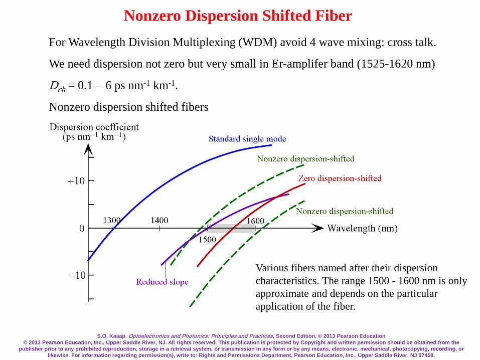
S.O. Kasap, Optoelectronics and Photonics: Principles and Practices, Second Edition, © 2013 Pearson Education© 2013 Pearson Education, Inc., Upper Saddle River, NJ. All rights reserved. This publication is protected by Copyright and written permission should be obtained from the
publisher prior to any prohibited reproduction, storage in a retrieval system, or transmission in any form or by any means, electronic, mechanical, photocopying, recording, or likewise. For information regarding permission(s), write to: Rights and Permissions Department, Pearson Education, Inc., Upper Saddle River, NJ 07458.
Nonzero Dispersion Shifted FiberFor Wavelength Division Multiplexing (WDM) avoid 4 wave mixing: cross talk.
We need dispersion not zero but very small in Er-amplifer band (1525-1620 nm)
Dch = 0.1 − 6 ps nm-1 km-1.
Nonzero dispersion shifted fibers
Various fibers named after their dispersion characteristics. The range 1500 - 1600 nm is only approximate and depends on the particular application of the fiber.

S.O. Kasap, Optoelectronics and Photonics: Principles and Practices, Second Edition, © 2013 Pearson Education© 2013 Pearson Education, Inc., Upper Saddle River, NJ. All rights reserved. This publication is protected by Copyright and written permission should be obtained from the
publisher prior to any prohibited reproduction, storage in a retrieval system, or transmission in any form or by any means, electronic, mechanical, photocopying, recording, or likewise. For information regarding permission(s), write to: Rights and Permissions Department, Pearson Education, Inc., Upper Saddle River, NJ 07458.
Dispersion Flattened Fiber
Dispersion flattened fiber example. The material dispersion coefficient (Dm) for thecore material and waveguide dispersion coefficient (Dw) for the doubly clad fiberresult in a flattened small chromatic dispersion between λ1 and λ2.

S.O. Kasap, Optoelectronics and Photonics: Principles and Practices, Second Edition, © 2013 Pearson Education© 2013 Pearson Education, Inc., Upper Saddle River, NJ. All rights reserved. This publication is protected by Copyright and written permission should be obtained from the
publisher prior to any prohibited reproduction, storage in a retrieval system, or transmission in any form or by any means, electronic, mechanical, photocopying, recording, or likewise. For information regarding permission(s), write to: Rights and Permissions Department, Pearson Education, Inc., Upper Saddle River, NJ 07458.
Nonzero Dispersion Shifted Fiber: More Examples
Nonzero dispersion shifted fiber (Corning)
Fiber with flattened dispersion slope
(schematic)
0.6%
0.4%

S.O. Kasap, Optoelectronics and Photonics: Principles and Practices, Second Edition, © 2013 Pearson Education© 2013 Pearson Education, Inc., Upper Saddle River, NJ. All rights reserved. This publication is protected by Copyright and written permission should be obtained from the
publisher prior to any prohibited reproduction, storage in a retrieval system, or transmission in any form or by any means, electronic, mechanical, photocopying, recording, or likewise. For information regarding permission(s), write to: Rights and Permissions Department, Pearson Education, Inc., Upper Saddle River, NJ 07458.
Commercial Fibers for Optical Communications
Fiber Dch
ps nm-1 km-1
S0
ps nm-2 km-1
DPMD
ps km-1/2
Some attributes
Standard single mode, ITU-T G.652
17
(1550 nm)
≤ 0.093 < 0.5
(cabled)
Dch = 0 at λ0 ≈ 1312 nm, MFD = 8.6 - 9.5 µm at 1310 nm. λc ≤1260 nm.
Non-zero dispersion shifted fiber, ITU-T G.655
0.1 − 6
(1530 nm)
< 0.05 at 1550 nm
< 0.5
(cabled)
For 1500 - 1600 nm range. WDM application
MFD = 8 − 11 µm.
Non-zero dispersion shifted fiber, ITU-T G.656
2 − 14 < 0.045 at 1550 nm
< 0.20
(cabled)
For 1460 - 1625 nm range. DWDM application. MFD = 7 − 11 µm (at 1550 nm). Positive Dch. λc<1310 nm
Corning SMF28e+
(Standard SMF)
18
(1550 nm)
0.088 < 0.1 Satisfies G.652. λ0 ≈ 1317 nm, MFD = 9.2 µm (at 1310 nm), 10.4 µm (at 1550 nm); λc ≤ 1260 nm.
OFS TrueWave RS Fiber 2.6 - 8.9 0.045 0.02 Satisfies G.655. Optimized for 1530 nm - 1625nm. MFD = 8.4 µm (at 1550 nm); λc ≤1260 nm.
OFS REACH Fiber 5.5 -8.9 0.045 0.02 Higher performance than G.655 specification. Satisfies G.656. For DWDM from 1460 to 1625 nm. λ0 ≤ 1405 nm. MFD = 8.6 µm (at 1550 nm)

S.O. Kasap, Optoelectronics and Photonics: Principles and Practices, Second Edition, © 2013 Pearson Education© 2013 Pearson Education, Inc., Upper Saddle River, NJ. All rights reserved. This publication is protected by Copyright and written permission should be obtained from the
publisher prior to any prohibited reproduction, storage in a retrieval system, or transmission in any form or by any means, electronic, mechanical, photocopying, recording, or likewise. For information regarding permission(s), write to: Rights and Permissions Department, Pearson Education, Inc., Upper Saddle River, NJ 07458.
Single Mode Fibers: Selected Examples

S.O. Kasap, Optoelectronics and Photonics: Principles and Practices, Second Edition, © 2013 Pearson Education© 2013 Pearson Education, Inc., Upper Saddle River, NJ. All rights reserved. This publication is protected by Copyright and written permission should be obtained from the
publisher prior to any prohibited reproduction, storage in a retrieval system, or transmission in any form or by any means, electronic, mechanical, photocopying, recording, or likewise. For information regarding permission(s), write to: Rights and Permissions Department, Pearson Education, Inc., Upper Saddle River, NJ 07458.
Dispersion Compensation
Total dispersion = DtLt + DcLc = (10 ps nm-1 km-1)(1000 km) +
(−100 ps nm-1 km-1)(80 km)
= 2000 ps/nm for 1080 km
Deffective = 1.9 ps nm-1 km-1

S.O. Kasap, Optoelectronics and Photonics: Principles and Practices, Second Edition, © 2013 Pearson Education© 2013 Pearson Education, Inc., Upper Saddle River, NJ. All rights reserved. This publication is protected by Copyright and written permission should be obtained from the
publisher prior to any prohibited reproduction, storage in a retrieval system, or transmission in any form or by any means, electronic, mechanical, photocopying, recording, or likewise. For information regarding permission(s), write to: Rights and Permissions Department, Pearson Education, Inc., Upper Saddle River, NJ 07458.
Dispersion Compensation
Dispersion D vs. wavelength characteristics involved in dispersion compensation. Inversedispersion fiber enables the dispersion to be reduced and maintained flat over the communicationwavelengths.

S.O. Kasap, Optoelectronics and Photonics: Principles and Practices, Second Edition, © 2013 Pearson Education© 2013 Pearson Education, Inc., Upper Saddle River, NJ. All rights reserved. This publication is protected by Copyright and written permission should be obtained from the
publisher prior to any prohibited reproduction, storage in a retrieval system, or transmission in any form or by any means, electronic, mechanical, photocopying, recording, or likewise. For information regarding permission(s), write to: Rights and Permissions Department, Pearson Education, Inc., Upper Saddle River, NJ 07458.
Dispersion Compensation and Management
Compensating fiber has higher attenuation. Doped core. Need shorter length
More susceptible to nonlinear effects.Use at the receiver end.
Different cross sections. Splicing/coupling losses.
Compensation depends on the temperature.
Manufacturers provide transmission fiber spliced to inverse dispersion fiber for a well defined D vs. λ

S.O. Kasap, Optoelectronics and Photonics: Principles and Practices, Second Edition, © 2013 Pearson Education© 2013 Pearson Education, Inc., Upper Saddle River, NJ. All rights reserved. This publication is protected by Copyright and written permission should be obtained from the
publisher prior to any prohibited reproduction, storage in a retrieval system, or transmission in any form or by any means, electronic, mechanical, photocopying, recording, or likewise. For information regarding permission(s), write to: Rights and Permissions Department, Pearson Education, Inc., Upper Saddle River, NJ 07458.
Dispersion and Maximum Bit Rate
B ≈0.5
∆τ1/ 2
Return-to-zero (RTZ) bit rate or data rate.
Nonreturn to zero (NRZ) bit rate = 2 RTZ bitrate

S.O. Kasap, Optoelectronics and Photonics: Principles and Practices, Second Edition, © 2013 Pearson Education© 2013 Pearson Education, Inc., Upper Saddle River, NJ. All rights reserved. This publication is protected by Copyright and written permission should be obtained from the
publisher prior to any prohibited reproduction, storage in a retrieval system, or transmission in any form or by any means, electronic, mechanical, photocopying, recording, or likewise. For information regarding permission(s), write to: Rights and Permissions Department, Pearson Education, Inc., Upper Saddle River, NJ 07458.
NRZ and RTZ
1 0 1 1 0 1 0 0 1
NRZ
RZ
Information
T

S.O. Kasap, Optoelectronics and Photonics: Principles and Practices, Second Edition, © 2013 Pearson Education© 2013 Pearson Education, Inc., Upper Saddle River, NJ. All rights reserved. This publication is protected by Copyright and written permission should be obtained from the
publisher prior to any prohibited reproduction, storage in a retrieval system, or transmission in any form or by any means, electronic, mechanical, photocopying, recording, or likewise. For information regarding permission(s), write to: Rights and Permissions Department, Pearson Education, Inc., Upper Saddle River, NJ 07458.
Maximum Bit Rate B
A Gaussian output light pulse and some tolerable intersymbol interference between two consecutive output light pulses (y-axis in relative units). At time t
= σ from the pulse center, the relative magnitude is e−1/2 = 0.607 and full width root mean square (rms) spread is ∆τrms = 2σ. (The RTZ case)

S.O. Kasap, Optoelectronics and Photonics: Principles and Practices, Second Edition, © 2013 Pearson Education© 2013 Pearson Education, Inc., Upper Saddle River, NJ. All rights reserved. This publication is protected by Copyright and written permission should be obtained from the
publisher prior to any prohibited reproduction, storage in a retrieval system, or transmission in any form or by any means, electronic, mechanical, photocopying, recording, or likewise. For information regarding permission(s), write to: Rights and Permissions Department, Pearson Education, Inc., Upper Saddle River, NJ 07458.
Dispersion and Maximum Bit Rate
2/1
59.025.0τσ ∆
=≈B 2/12/1 λτ
∆=∆
chDL
Maximum Bit Rate Dispersion
2/12/1
59.059.0λτ ∆
=∆
≈chD
BL
Bit Rate × Distance is
inversely proportional to dispersion
inversely proportional to line width of laser
(so, we need single frequency lasers!)

S.O. Kasap, Optoelectronics and Photonics: Principles and Practices, Second Edition, © 2013 Pearson Education© 2013 Pearson Education, Inc., Upper Saddle River, NJ. All rights reserved. This publication is protected by Copyright and written permission should be obtained from the
publisher prior to any prohibited reproduction, storage in a retrieval system, or transmission in any form or by any means, electronic, mechanical, photocopying, recording, or likewise. For information regarding permission(s), write to: Rights and Permissions Department, Pearson Education, Inc., Upper Saddle River, NJ 07458.
Dispersion and Maximum Bit Rate
B ≈0.25
σ=
0.59∆τ1/2
Maximum Bit Rate
2intramodal
2intermodal σσσ +=2
2intramodal2/1
2intermodal2/1
22/1 )()()( τττ ∆+∆=∆
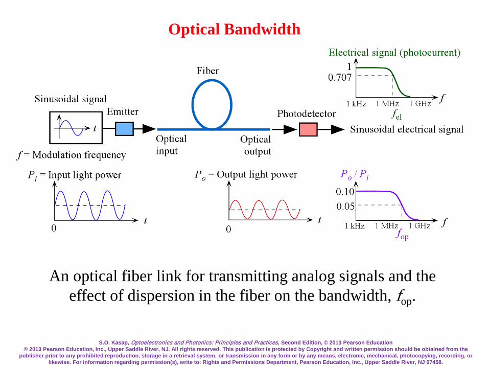
S.O. Kasap, Optoelectronics and Photonics: Principles and Practices, Second Edition, © 2013 Pearson Education© 2013 Pearson Education, Inc., Upper Saddle River, NJ. All rights reserved. This publication is protected by Copyright and written permission should be obtained from the
publisher prior to any prohibited reproduction, storage in a retrieval system, or transmission in any form or by any means, electronic, mechanical, photocopying, recording, or likewise. For information regarding permission(s), write to: Rights and Permissions Department, Pearson Education, Inc., Upper Saddle River, NJ 07458.
Optical Bandwidth
An optical fiber link for transmitting analog signals and the effect of dispersion in the fiber on the bandwidth, fop.

S.O. Kasap, Optoelectronics and Photonics: Principles and Practices, Second Edition, © 2013 Pearson Education© 2013 Pearson Education, Inc., Upper Saddle River, NJ. All rights reserved. This publication is protected by Copyright and written permission should be obtained from the
publisher prior to any prohibited reproduction, storage in a retrieval system, or transmission in any form or by any means, electronic, mechanical, photocopying, recording, or likewise. For information regarding permission(s), write to: Rights and Permissions Department, Pearson Education, Inc., Upper Saddle River, NJ 07458.
Pulse Shape and Maximum Bit Rate

S.O. Kasap, Optoelectronics and Photonics: Principles and Practices, Second Edition, © 2013 Pearson Education© 2013 Pearson Education, Inc., Upper Saddle River, NJ. All rights reserved. This publication is protected by Copyright and written permission should be obtained from the
publisher prior to any prohibited reproduction, storage in a retrieval system, or transmission in any form or by any means, electronic, mechanical, photocopying, recording, or likewise. For information regarding permission(s), write to: Rights and Permissions Department, Pearson Education, Inc., Upper Saddle River, NJ 07458.
Example: Bit rate and dispersionConsider an optical fiber with a chromatic dispersion coefficient 8 ps km-1 nm-1
at an operating wavelength of 1.5 µm. Calculate the bit rate distance product (BL), and the optical and electrical bandwidths for a 10 km fiber if a laser diode source with a FWHP linewidth ∆λ1/2 of 2 nm is used.Solution
For FWHP dispersion,∆τ1/2/L = |Dch|∆λ1/2 = (8 ps nm-1 km-1)(2 nm) = 16 ps km-1
Assuming a Gaussian light pulse shape, the RTZ bit rate × distance product (BL) is
BL = 0.59L/∆τ1/2 = 0.59/(16 ps km-1) = 36.9 Gb s-1 kmThe optical and electrical bandwidths for a 10 km fiber are
fop = 0.75B = 0.75(36.9 Gb s-1 km) / (10 km) = 2.8 GHzfel = 0.70fop = 1.9 GHz

S.O. Kasap, Optoelectronics and Photonics: Principles and Practices, Second Edition, © 2013 Pearson Education© 2013 Pearson Education, Inc., Upper Saddle River, NJ. All rights reserved. This publication is protected by Copyright and written permission should be obtained from the
publisher prior to any prohibited reproduction, storage in a retrieval system, or transmission in any form or by any means, electronic, mechanical, photocopying, recording, or likewise. For information regarding permission(s), write to: Rights and Permissions Department, Pearson Education, Inc., Upper Saddle River, NJ 07458.
Graded Index (GRIN) Fiber
(a) Multimode step index fiber. Ray paths are different so that rays arrive at different times.
(b) Graded index fiber. Ray paths are different but so are the velocities along the paths so that all the rays arrive at the same time.

S.O. Kasap, Optoelectronics and Photonics: Principles and Practices, Second Edition, © 2013 Pearson Education© 2013 Pearson Education, Inc., Upper Saddle River, NJ. All rights reserved. This publication is protected by Copyright and written permission should be obtained from the
publisher prior to any prohibited reproduction, storage in a retrieval system, or transmission in any form or by any means, electronic, mechanical, photocopying, recording, or likewise. For information regarding permission(s), write to: Rights and Permissions Department, Pearson Education, Inc., Upper Saddle River, NJ 07458.
(a) A ray in thinly stratifed medium becomes refracted as it passes from one layer to the next upper layer with lower nand eventually its angle satisfies TIR.
(b) In a medium where n decreases continuously the path of the ray bends continuously.
Graded Index (GRIN) Fiber

S.O. Kasap, Optoelectronics and Photonics: Principles and Practices, Second Edition, © 2013 Pearson Education© 2013 Pearson Education, Inc., Upper Saddle River, NJ. All rights reserved. This publication is protected by Copyright and written permission should be obtained from the
publisher prior to any prohibited reproduction, storage in a retrieval system, or transmission in any form or by any means, electronic, mechanical, photocopying, recording, or likewise. For information regarding permission(s), write to: Rights and Permissions Department, Pearson Education, Inc., Upper Saddle River, NJ 07458.
Graded Index (GRIN) Fiber
The refractive index profile cangenerally be described by a power lawwith an index γ called the profile index(or the coefficient of index grating) sothat,n = n1[1 − 2∆(r/a)γ]1/2 ; r < a,
n = n2 ; r ≥ a
σ intermode
L≈
n1
20 3c∆2
Minimum intermodal dispersion
Minimum intermodal dispersion
225
)3)(4(2 ≈+
++∆−+≈
δδδδγ o

S.O. Kasap, Optoelectronics and Photonics: Principles and Practices, Second Edition, © 2013 Pearson Education© 2013 Pearson Education, Inc., Upper Saddle River, NJ. All rights reserved. This publication is protected by Copyright and written permission should be obtained from the
publisher prior to any prohibited reproduction, storage in a retrieval system, or transmission in any form or by any means, electronic, mechanical, photocopying, recording, or likewise. For information regarding permission(s), write to: Rights and Permissions Department, Pearson Education, Inc., Upper Saddle River, NJ 07458.
Graded Index (GRIN) Fiber
σ intermode
L≈
n1
20 3c∆2
Minimum intermodal dispersion
Minimum intermodal dispersion
225
)3)(4(2 ≈+
++∆−+≈
δδδδγ o
λλδ
dd
Nn ∆
∆−=
1
1
g
Profile dispersion parameter

S.O. Kasap, Optoelectronics and Photonics: Principles and Practices, Second Edition, © 2013 Pearson Education© 2013 Pearson Education, Inc., Upper Saddle River, NJ. All rights reserved. This publication is protected by Copyright and written permission should be obtained from the
publisher prior to any prohibited reproduction, storage in a retrieval system, or transmission in any form or by any means, electronic, mechanical, photocopying, recording, or likewise. For information regarding permission(s), write to: Rights and Permissions Department, Pearson Education, Inc., Upper Saddle River, NJ 07458.
Graded Index (GRIN) Fiber
2/122
2 ])([)(NANA nrnr −==
2/122
21
2/1GRIN ))(2/1(NA nn −≈
Effective numerical aperture for GRIN fibers
22
2VM
+
≈γ
γ
Number of modes in a graded index fiber

S.O. Kasap, Optoelectronics and Photonics: Principles and Practices, Second Edition, © 2013 Pearson Education© 2013 Pearson Education, Inc., Upper Saddle River, NJ. All rights reserved. This publication is protected by Copyright and written permission should be obtained from the
publisher prior to any prohibited reproduction, storage in a retrieval system, or transmission in any form or by any means, electronic, mechanical, photocopying, recording, or likewise. For information regarding permission(s), write to: Rights and Permissions Department, Pearson Education, Inc., Upper Saddle River, NJ 07458.
Table 2.5Graded index multimode fibers
d = core diameter (µm), D = cladding diameter (µm). Typical properties at 850 nm. VCSEL is a vertical cavity surface emitting laser. α is attenuation along the fiber. OM1, OM3 and OM4 are fiber standards for LAN data links (ethernet). α are reported typical attenuation values. 10G and 40G networks represent data rates of 10 Gb s-1 and 40 Gb s-1 and correspond to 10 GbE (Gigabit Ethernet) and 40 GbE systems.
MMF d/D
Compliance standard
Source Typical Dch
ps nm-1 km-1
Bandwidth
MHz⋅km
ΝΑ α
dB km-1
Reach in 10G and 40G networks
50/125 OM4 VCSEL −100 4700 (EMB)
3500 (OFLBW)
0.200 < 3 550 m (10G)
150 m (40G)
50/125 OM3 VCSEL −100 2000 (EMB)
500 (OFLBW)
0.200 < 3 300 m (10G)
62.5/125 OM1 LED −117 200 (OFLBW) 0.275 < 3 33 m (10G)

S.O. Kasap, Optoelectronics and Photonics: Principles and Practices, Second Edition, © 2013 Pearson Education© 2013 Pearson Education, Inc., Upper Saddle River, NJ. All rights reserved. This publication is protected by Copyright and written permission should be obtained from the
publisher prior to any prohibited reproduction, storage in a retrieval system, or transmission in any form or by any means, electronic, mechanical, photocopying, recording, or likewise. For information regarding permission(s), write to: Rights and Permissions Department, Pearson Education, Inc., Upper Saddle River, NJ 07458.
Example: Dispersion in a GRIN Fiber and Bit RateGraded index fiber. Diameter of 50 µm and a refractive index of n1 = 1.4750, ∆ = 0.010.The fiber is used in LANs at 850 nm with a vertical cavity surface emitting laser (VCSEL) that has very anarrow linewidth that is about 0.4 nm (FWHM). Assume that the chromatic dispersion at 850 nm is −100ps nm-1 km-1 as shown in Table 2.5. Assume the fiber has been optimized at 850 nm, and find the minimumrms dispersion. How many modes are there? What would be the upper limit on its bandwidth? What wouldbe the bandwidth in practice?
Solution
Given ∆ and n1, we can find n2 from ∆ = 0.01 = (n1 − n2)/n1 = (1.4750 − n2)/1.4750. ∴ n2 = 1.4603. The V-number is thenV = [(2π)(25 µm)/(0.850 µm)(1.47502−1.46032)1/2 = 38.39For the number of modes we can simply take γ = 2 and useM = (V2/4) = (38.392/4) = 368 modes The lowest intermodal dispersion for a profile optimized graded index fiber for a 1 km of fiber, L = 1 km, is

S.O. Kasap, Optoelectronics and Photonics: Principles and Practices, Second Edition, © 2013 Pearson Education© 2013 Pearson Education, Inc., Upper Saddle River, NJ. All rights reserved. This publication is protected by Copyright and written permission should be obtained from the
publisher prior to any prohibited reproduction, storage in a retrieval system, or transmission in any form or by any means, electronic, mechanical, photocopying, recording, or likewise. For information regarding permission(s), write to: Rights and Permissions Department, Pearson Education, Inc., Upper Saddle River, NJ 07458.
Example: Dispersion in a GRIN Fiber and Bit RateSolution continued
28
21intermode )010.0()103(320
4750.1320 ×
=∆≈c
nL
σ
= 14.20×10⁻¹⁵ s m-1 or 14.20 ps km-1
Assuming a triangular output light pulse and the relationship between σ and ∆τ1/2given in Table 2.4, the intermodal spread ∆τintermode (FWHM) in the group delay over 1 km is
∆τintermode = (61/2)σintermode = (2.45)(14.20 ps) = 34.8 ps
We also need the material dispersion at the operating wavelength over 1 km, which makes up the intramodal dispersion ∆τintramode (FWHM)∆τintramode = L|Dch| ∆λ1/2 = (1 km)(−100 ps nm-1 km-1)(0.40 nm) = 40.0 ps
222intramode
2intermode
2 )0.40()8.34( +=∆+∆=∆ τττ ∆τ = 53.0 ps

S.O. Kasap, Optoelectronics and Photonics: Principles and Practices, Second Edition, © 2013 Pearson Education© 2013 Pearson Education, Inc., Upper Saddle River, NJ. All rights reserved. This publication is protected by Copyright and written permission should be obtained from the
publisher prior to any prohibited reproduction, storage in a retrieval system, or transmission in any form or by any means, electronic, mechanical, photocopying, recording, or likewise. For information regarding permission(s), write to: Rights and Permissions Department, Pearson Education, Inc., Upper Saddle River, NJ 07458.
Example: Dispersion in a GRIN Fiber and Bit RateSolution continued
)s100.53(61.061.0
408.025.025.0
12−×=
∆=
∆==
ττσB = 11.5 Gb s-1
Optical bandwidth fop = 0.99B = 11.4 GHz
This is the upper limit since we assumed that the graded index fiber is perfectly optimized with σintermode being minimum. Small deviations around the optimum γ cause large increases in σintermode, which would sharply reduce the bandwidth.

S.O. Kasap, Optoelectronics and Photonics: Principles and Practices, Second Edition, © 2013 Pearson Education© 2013 Pearson Education, Inc., Upper Saddle River, NJ. All rights reserved. This publication is protected by Copyright and written permission should be obtained from the
publisher prior to any prohibited reproduction, storage in a retrieval system, or transmission in any form or by any means, electronic, mechanical, photocopying, recording, or likewise. For information regarding permission(s), write to: Rights and Permissions Department, Pearson Education, Inc., Upper Saddle River, NJ 07458.
Example: Dispersion in a GRIN Fiber and Bit RateSolution continued
If this were a multimode step-index fiber with the same n1 and n2, then the full dispersion (total spread) would roughly be
8121
103)01.0)(475.1(
×=
∆=
−≈
∆c
nc
nnLτ
= 4.92×10⁻¹¹ s m-1 or 49.2 ns km-1
To calculate the BL we use σintermode ≈ 0.29∆τ
)km s 102.49)(29.0(25.0
)/(29.025.025.0
19intermode
−−×=
∆=≈
LLBL
τσ= 17.5 Mb s-1 km
LANs now use graded index MMFs, and the step index MMFs are used mainly in low speed instrumentation

S.O. Kasap, Optoelectronics and Photonics: Principles and Practices, Second Edition, © 2013 Pearson Education© 2013 Pearson Education, Inc., Upper Saddle River, NJ. All rights reserved. This publication is protected by Copyright and written permission should be obtained from the
publisher prior to any prohibited reproduction, storage in a retrieval system, or transmission in any form or by any means, electronic, mechanical, photocopying, recording, or likewise. For information regarding permission(s), write to: Rights and Permissions Department, Pearson Education, Inc., Upper Saddle River, NJ 07458.
Example: Dispersion in a graded-index fiber and bit rateConsider a graded index fiber whose core has a diameter of 50 µm and a refractive index of n1 = 1.480. The cladding has n2 = 1.460. If this fiber is used at 1.30 µm with a laser diode that has very a narrow linewidth what will be the bit rate × distance product? Evaluate the BL product if this were a multimode step index fiber.Solution The normalized refractive index difference ∆ = (n1 − n2)/n1 = (1.48 − 1.46)/1.48 = 0.0135. Dispersion for 1 km of fiber isσintermode/L = n1∆2/[(20)(31/2)c] = 2.6×10⁻¹⁴ s m-1 or 0.026 ns km-1.BL = 0.25/σintermode = 9.6 Gb s-1 kmWe have ignored any material dispersion and, further, we assumed the index variation to perfectly follow the optimal profile which means that in practice BL will be worse. (For example, a 15% variation in γ from the optimal value can result in σintermode and hence BLthat are more than 10 times worse.)If this were a multimode step-index fiber with the same n1 and n2, then the full dispersion (total spread) would roughly be 6.67×10⁻¹¹ s m-1 or 66.7 ns km-1 and BL = 12.9 Mb s-1
kmNote: Over long distances, the bit rate × distance product is not constant for multimode fibers and typically B ∝ L−γ where γ is an index between 0.5 and 1. The reason is that, due to various fiber imperfections, there is mode mixing which reduces the extent of spreading.

S.O. Kasap, Optoelectronics and Photonics: Principles and Practices, Second Edition, © 2013 Pearson Education© 2013 Pearson Education, Inc., Upper Saddle River, NJ. All rights reserved. This publication is protected by Copyright and written permission should be obtained from the
publisher prior to any prohibited reproduction, storage in a retrieval system, or transmission in any form or by any means, electronic, mechanical, photocopying, recording, or likewise. For information regarding permission(s), write to: Rights and Permissions Department, Pearson Education, Inc., Upper Saddle River, NJ 07458.
Example: Combining intermodal and intramodal dispersionsConsider a graded index fiber with a core diameter of 30 µm and a refractive index of 1.474 at the center of the core and a cladding refractive index of 1.453. Suppose that we use a laser diode emitter with a spectral linewidth of 3 nm to transmit along this fiber at a wavelength of 1300 nm. Calculate, the total dispersion and estimate the bit-rate × distance product of the fiber. The material dispersion coefficient Dm at 1300 nm is −7.5 ps nm-1 km-1.
SolutionThe normalized refractive index difference ∆ = (n1 − n2)/n1 = (1.474 − 1.453)/1.474 = 0.01425. Modal dispersion for 1 km isσintermode = Ln1∆2/[(20)(31/2)c] = 2.9×10⁻¹¹ s 1 or 0.029 ns.The material dispersion is∆τ1/2 = LDm ∆λ1/2 = (1 km)(7.5 ps nm-1 km-1)(3 nm) = 0.0225 nsAssuming a Gaussian output light pulse shape, σintramode = 0.425∆τ1/2 = (0.425)(0.0225 ns) = 0.0096 nsTotal dispersion is
σ rms = σ intermode2 +σ intramode
2 = 0.0292 + 0.00962 = 0.030 ns
B = 0.25/∆τrms = 8.2 Gb
Assume L = 1 km

S.O. Kasap, Optoelectronics and Photonics: Principles and Practices, Second Edition, © 2013 Pearson Education© 2013 Pearson Education, Inc., Upper Saddle River, NJ. All rights reserved. This publication is protected by Copyright and written permission should be obtained from the
publisher prior to any prohibited reproduction, storage in a retrieval system, or transmission in any form or by any means, electronic, mechanical, photocopying, recording, or likewise. For information regarding permission(s), write to: Rights and Permissions Department, Pearson Education, Inc., Upper Saddle River, NJ 07458.
GRIN Rod Lenses
Point O is on the rod face center and the lens focuses the rays
onto O' on to the center of the opposite face.
One pitch (P) is a full one period variation in the ray trajectory along the rod axis.
The rays from Oon the rod face
center are collimated out.
O is slightly away from the rod face and the
rays are collimated out.

S.O. Kasap, Optoelectronics and Photonics: Principles and Practices, Second Edition, © 2013 Pearson Education© 2013 Pearson Education, Inc., Upper Saddle River, NJ. All rights reserved. This publication is protected by Copyright and written permission should be obtained from the
publisher prior to any prohibited reproduction, storage in a retrieval system, or transmission in any form or by any means, electronic, mechanical, photocopying, recording, or likewise. For information regarding permission(s), write to: Rights and Permissions Department, Pearson Education, Inc., Upper Saddle River, NJ 07458.
Attenuation
Attenuation = Absorption + ScatteringAttenuation coefficient α is defined as the fractional decrease in the optical power per unit distance. α is in m-1.Pout = Pinexp(−αL)
=
out
indB log101
PP
Lα ααα 34.4
)10ln(10
dB ==
The attenuation of light in a medium
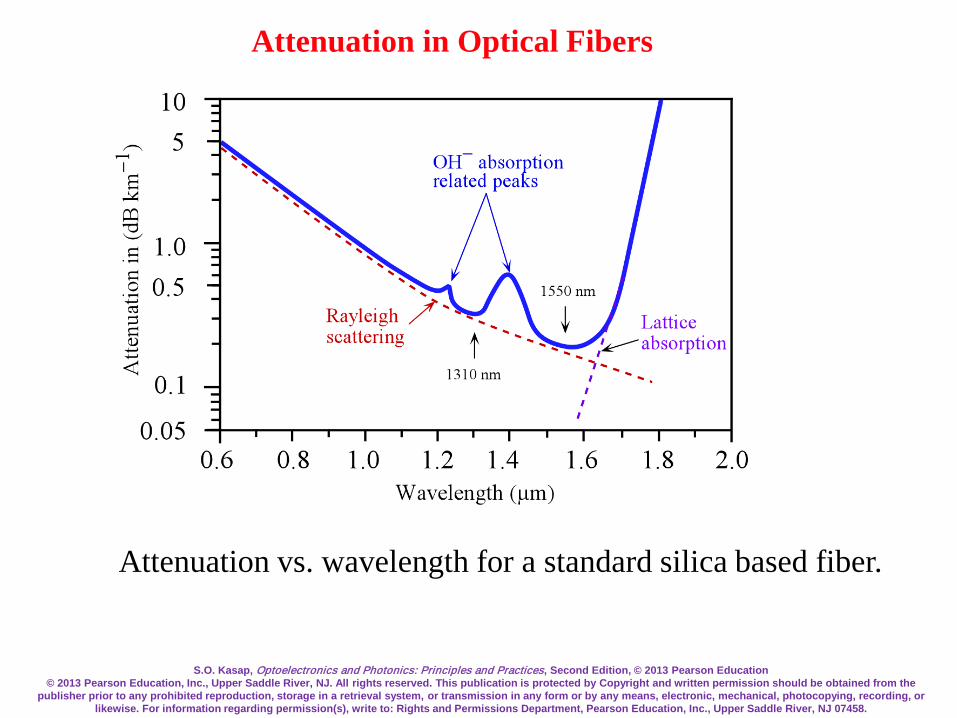
S.O. Kasap, Optoelectronics and Photonics: Principles and Practices, Second Edition, © 2013 Pearson Education© 2013 Pearson Education, Inc., Upper Saddle River, NJ. All rights reserved. This publication is protected by Copyright and written permission should be obtained from the
publisher prior to any prohibited reproduction, storage in a retrieval system, or transmission in any form or by any means, electronic, mechanical, photocopying, recording, or likewise. For information regarding permission(s), write to: Rights and Permissions Department, Pearson Education, Inc., Upper Saddle River, NJ 07458.
Attenuation in Optical Fibers
Attenuation vs. wavelength for a standard silica based fiber.

S.O. Kasap, Optoelectronics and Photonics: Principles and Practices, Second Edition, © 2013 Pearson Education© 2013 Pearson Education, Inc., Upper Saddle River, NJ. All rights reserved. This publication is protected by Copyright and written permission should be obtained from the
publisher prior to any prohibited reproduction, storage in a retrieval system, or transmission in any form or by any means, electronic, mechanical, photocopying, recording, or likewise. For information regarding permission(s), write to: Rights and Permissions Department, Pearson Education, Inc., Upper Saddle River, NJ 07458.
Lattice Absorption (Reststrahlen Absorption)
EM Wave oscillations are coupled to lattice vibrations (phonons), vibrations of the ions in the lattice. Energy is transferred from the EM wave to these lattice vibrations.
This corresponds to “Fundamental Infrared Absorption” in glasses

S.O. Kasap, Optoelectronics and Photonics: Principles and Practices, Second Edition, © 2013 Pearson Education© 2013 Pearson Education, Inc., Upper Saddle River, NJ. All rights reserved. This publication is protected by Copyright and written permission should be obtained from the
publisher prior to any prohibited reproduction, storage in a retrieval system, or transmission in any form or by any means, electronic, mechanical, photocopying, recording, or likewise. For information regarding permission(s), write to: Rights and Permissions Department, Pearson Education, Inc., Upper Saddle River, NJ 07458.
Rayleigh Scattering
Rayleigh scattering involves the polarization of a small dielectric particle or a regionthat is much smaller than the light wavelength. The field forces dipole oscillations inthe particle (by polarizing it) which leads to the emission of EM waves in "many"directions so that a portion of the light energy is directed away from the incident beam.
αR ≈8π 3
3λ4 n2 −1( )2βTkBTf
βΤ = isothermal compressibility (at Tf)
Tf = fictive temperature (roughly thesoftening temperature of glass) wherethe liquid structure during the coolingof the fiber is frozen to become theglass structure

S.O. Kasap, Optoelectronics and Photonics: Principles and Practices, Second Edition, © 2013 Pearson Education© 2013 Pearson Education, Inc., Upper Saddle River, NJ. All rights reserved. This publication is protected by Copyright and written permission should be obtained from the
publisher prior to any prohibited reproduction, storage in a retrieval system, or transmission in any form or by any means, electronic, mechanical, photocopying, recording, or likewise. For information regarding permission(s), write to: Rights and Permissions Department, Pearson Education, Inc., Upper Saddle River, NJ 07458.
Example: Rayleigh scattering limitWhat is the attenuation due to Rayleigh scattering at around the λ = 1.55 µm window given that pure silica (SiO2) has the following properties: Tf = 1730°C (softening temperature); βT = 7×10-11 m2 N-1 (at high temperatures); n = 1.4446 at 1.5 µm.SolutionWe simply calculate the Rayleigh scattering attenuation using
αR ≈8π 3
3λ4 (n2 −1)2βTkBTf
αR ≈8π 3
3(1.55 ×10⁻⁶)4 (1.44462 −1)2(7 ×10⁻¹¹)(1.38 ×10⁻²³)(1730 + 273)
αR = 3.276×10⁻⁵ m-1 or 3.276×10⁻² km-1
Attenuation in dB per km is αdB = 4.34αR = (4.34)(3.735×10⁻² km-1) = 0.142 dB km-1
This represents the lowest possible attenuation for a silica glass core fiber at 1.55 µm.

S.O. Kasap, Optoelectronics and Photonics: Principles and Practices, Second Edition, © 2013 Pearson Education© 2013 Pearson Education, Inc., Upper Saddle River, NJ. All rights reserved. This publication is protected by Copyright and written permission should be obtained from the
publisher prior to any prohibited reproduction, storage in a retrieval system, or transmission in any form or by any means, electronic, mechanical, photocopying, recording, or likewise. For information regarding permission(s), write to: Rights and Permissions Department, Pearson Education, Inc., Upper Saddle River, NJ 07458.
Attenuation in Optical Fibers
Attenuation vs. wavelength for a standard silica based fiber.

S.O. Kasap, Optoelectronics and Photonics: Principles and Practices, Second Edition, © 2013 Pearson Education© 2013 Pearson Education, Inc., Upper Saddle River, NJ. All rights reserved. This publication is protected by Copyright and written permission should be obtained from the
publisher prior to any prohibited reproduction, storage in a retrieval system, or transmission in any form or by any means, electronic, mechanical, photocopying, recording, or likewise. For information regarding permission(s), write to: Rights and Permissions Department, Pearson Education, Inc., Upper Saddle River, NJ 07458.
Low-water-peak fiber has no OH- peak
E-band is available for communications with this fiber

S.O. Kasap, Optoelectronics and Photonics: Principles and Practices, Second Edition, © 2013 Pearson Education© 2013 Pearson Education, Inc., Upper Saddle River, NJ. All rights reserved. This publication is protected by Copyright and written permission should be obtained from the
publisher prior to any prohibited reproduction, storage in a retrieval system, or transmission in any form or by any means, electronic, mechanical, photocopying, recording, or likewise. For information regarding permission(s), write to: Rights and Permissions Department, Pearson Education, Inc., Upper Saddle River, NJ 07458.
( )λα /expFIR BA −=4λ
α RR
A=
Attenuation in Optical Fibers

S.O. Kasap, Optoelectronics and Photonics: Principles and Practices, Second Edition, © 2013 Pearson Education© 2013 Pearson Education, Inc., Upper Saddle River, NJ. All rights reserved. This publication is protected by Copyright and written permission should be obtained from the
publisher prior to any prohibited reproduction, storage in a retrieval system, or transmission in any form or by any means, electronic, mechanical, photocopying, recording, or likewise. For information regarding permission(s), write to: Rights and Permissions Department, Pearson Education, Inc., Upper Saddle River, NJ 07458.
Attenuation
( )λα /expFIR BA −=
4λα R
RA
=AR in dB km-1 µm4
λ in µm
αR in dB km-1

S.O. Kasap, Optoelectronics and Photonics: Principles and Practices, Second Edition, © 2013 Pearson Education© 2013 Pearson Education, Inc., Upper Saddle River, NJ. All rights reserved. This publication is protected by Copyright and written permission should be obtained from the
publisher prior to any prohibited reproduction, storage in a retrieval system, or transmission in any form or by any means, electronic, mechanical, photocopying, recording, or likewise. For information regarding permission(s), write to: Rights and Permissions Department, Pearson Education, Inc., Upper Saddle River, NJ 07458.
Attenuation
Glass AR
dB km-1 µm4
Comment Glass
Silica fiber 0.90 "Rule of thumb" Silica fiber
SiO2-GeO2 core step index fiber
0.63 + 2.06×NA NA depends on (n12 – n2
2)1/2
and hence on the doping difference.
SiO2-GeO2 core step index fiber
SiO2-GeO2 core graded index fiber
0.63 + 1.75×NA SiO2-GeO2 core graded index fiber
Silica, SiO2 0.63 Measured on preforms. Depends on annealing. AR(Silica) = 0.59 dB km-1 µm4
for annealed.
Silica, SiO2
65%SiO235%GeO2 0.75 On a preform. AR/AR(silica) = 1.19
65%SiO235%GeO2
(SiO2)1−x(GeO2)x AR(silica)×(1 + 0.62x) x = [GeO2] = Concentration as a fraction (10% GeO2, x = 0.1). For preform.
(SiO2)1−x(GeO2)x
Approximate attenuation coefficients for silica-based fibers for use in Equations (7) and (8). Squarebrackets represent concentration as a fraction. NA = Numerical Aperture. AR = 0.59 used as referencefor pure silica, and represents AR(silica). Data mainly from K. Tsujikawa et al, Electron. Letts., 30, 351,1994; Opt. Fib. Technol. 11, 319, 2005, H. Hughes, Telecommunications Cables (John Wiley and Sons,1999, and references therein.)

S.O. Kasap, Optoelectronics and Photonics: Principles and Practices, Second Edition, © 2013 Pearson Education© 2013 Pearson Education, Inc., Upper Saddle River, NJ. All rights reserved. This publication is protected by Copyright and written permission should be obtained from the
publisher prior to any prohibited reproduction, storage in a retrieval system, or transmission in any form or by any means, electronic, mechanical, photocopying, recording, or likewise. For information regarding permission(s), write to: Rights and Permissions Department, Pearson Education, Inc., Upper Saddle River, NJ 07458.
Rayleigh ScatteringExample: Consider a single mode step index fiber, which has a numericalaperture of 0.14. Predict the expected attenuation at 1.55 µm, and compare yourcalculation with the reported (measured) value of 0.19 - 0.20 dB km-1 for thisfiber. Repeat the calculations at 1.31 µm, and compare your values with thereported 0.33 - 0.35 dB km-1 values.
( ) )]55.1/()5.48(exp[108.7/exp 11FIR −×=−= λα BA
SolutionFirst, we should check the fundamental infrared absorption at 1550 nm.
= 0.020 dB km-1, very small

S.O. Kasap, Optoelectronics and Photonics: Principles and Practices, Second Edition, © 2013 Pearson Education© 2013 Pearson Education, Inc., Upper Saddle River, NJ. All rights reserved. This publication is protected by Copyright and written permission should be obtained from the
publisher prior to any prohibited reproduction, storage in a retrieval system, or transmission in any form or by any means, electronic, mechanical, photocopying, recording, or likewise. For information regarding permission(s), write to: Rights and Permissions Department, Pearson Education, Inc., Upper Saddle River, NJ 07458.
SolutionRayleigh scattering at 1550 nm, the simplest equation with AR = 0.9 dB km-1
µm4, givesαR = AR/λ4 = (0.90 dB km-1 µm4)/(1.55 µm)4 = 0.178 dB km-1
This equation is basically a rule of thumb. The total attenuation is then
αR + αFIR = 0.178 + 0.02 = 0.198 dB km-1.
The current fiber has NA = 0.14. ∴ AR = 0.63 + 2.06×NA = 0.63 + 2.06×0.14 = 0.918 dB km-1 µm4
i.e. αR = AR/λ4 = (0.918 dB km-1 µm4)/(1.55 µm)4 = 0.159 dB km-1, which gives a total attenuation of 0.159 + 0.020 or 0.179 dB km-1.
Rayleigh Scattering

S.O. Kasap, Optoelectronics and Photonics: Principles and Practices, Second Edition, © 2013 Pearson Education© 2013 Pearson Education, Inc., Upper Saddle River, NJ. All rights reserved. This publication is protected by Copyright and written permission should be obtained from the
publisher prior to any prohibited reproduction, storage in a retrieval system, or transmission in any form or by any means, electronic, mechanical, photocopying, recording, or likewise. For information regarding permission(s), write to: Rights and Permissions Department, Pearson Education, Inc., Upper Saddle River, NJ 07458.
Solution
We can repeat the above calculations at λ = 1.31 µm. However, we do not need to add αFIR.
αR = AR/λ4 = (0.90 dB km-1 µm4)/(1.31 µm)4 = 0.306 dB km-1
and using the NA based for AR,
αR = AR/λ4 = (0.918 dB km-1 µm4)/(1.31 µm)4 = 0.312 dB km-1.
Both close to the measured value.
Rayleigh Scattering

S.O. Kasap, Optoelectronics and Photonics: Principles and Practices, Second Edition, © 2013 Pearson Education© 2013 Pearson Education, Inc., Upper Saddle River, NJ. All rights reserved. This publication is protected by Copyright and written permission should be obtained from the
publisher prior to any prohibited reproduction, storage in a retrieval system, or transmission in any form or by any means, electronic, mechanical, photocopying, recording, or likewise. For information regarding permission(s), write to: Rights and Permissions Department, Pearson Education, Inc., Upper Saddle River, NJ 07458.
Bending Loss
Definitions of (a) microbending and (b) macrobending loss and the definition of the radius of curvature, R. (A schematic illustration only.) The propagating mode
in the fiber is shown as white painted area. Some radiation is lost in the region where the fiber is bent. D is the fiber diameter, including the cladding.

S.O. Kasap, Optoelectronics and Photonics: Principles and Practices, Second Edition, © 2013 Pearson Education© 2013 Pearson Education, Inc., Upper Saddle River, NJ. All rights reserved. This publication is protected by Copyright and written permission should be obtained from the
publisher prior to any prohibited reproduction, storage in a retrieval system, or transmission in any form or by any means, electronic, mechanical, photocopying, recording, or likewise. For information regarding permission(s), write to: Rights and Permissions Department, Pearson Education, Inc., Upper Saddle River, NJ 07458.
Bending Loss
Microbending loss
the radius of curvature R of the bend is sharpbend radius is comparable to the diameter of the fiber
Typically microbending losses are significant when the radius of curvature of the bend is less than 0.1 − 1 mm.
They can arise from careless or poor cabling of the fiber or even in flaws in manufacturing that result in variations in the fiber geometry over small distances.

S.O. Kasap, Optoelectronics and Photonics: Principles and Practices, Second Edition, © 2013 Pearson Education© 2013 Pearson Education, Inc., Upper Saddle River, NJ. All rights reserved. This publication is protected by Copyright and written permission should be obtained from the
publisher prior to any prohibited reproduction, storage in a retrieval system, or transmission in any form or by any means, electronic, mechanical, photocopying, recording, or likewise. For information regarding permission(s), write to: Rights and Permissions Department, Pearson Education, Inc., Upper Saddle River, NJ 07458.
Bending Loss
Macrobending lossesLosses that arise when the bend is much larger than the fiber sizeTypically much grater than 1 mmTypically occur when the fiber is bent during the installation of a fiber optic link such
as turning the fiber around a corner.
There is no simple precise and sharp boundary line between microbending andmacrobending loss definitions.
Both losses essentially result from changes in the waveguide geometry and properties asthe fiber is subjected to external forces that bend the fiber.
Typically, macrobending loss crosses over into microbending loss when the radius ofcurvature becomes less than a few millimeters.

S.O. Kasap, Optoelectronics and Photonics: Principles and Practices, Second Edition, © 2013 Pearson Education© 2013 Pearson Education, Inc., Upper Saddle River, NJ. All rights reserved. This publication is protected by Copyright and written permission should be obtained from the
publisher prior to any prohibited reproduction, storage in a retrieval system, or transmission in any form or by any means, electronic, mechanical, photocopying, recording, or likewise. For information regarding permission(s), write to: Rights and Permissions Department, Pearson Education, Inc., Upper Saddle River, NJ 07458.
Bending Loss
Sharp bends change the local waveguide geometry that can lead to waves escaping. The zigzagging ray suddenly finds itself with an incidence angle smaller than θ′ that gives rise to either a transmitted wave, or to a greater cladding penetration; the field reaches
the outside medium and some light energy is lost.

S.O. Kasap, Optoelectronics and Photonics: Principles and Practices, Second Edition, © 2013 Pearson Education© 2013 Pearson Education, Inc., Upper Saddle River, NJ. All rights reserved. This publication is protected by Copyright and written permission should be obtained from the
publisher prior to any prohibited reproduction, storage in a retrieval system, or transmission in any form or by any means, electronic, mechanical, photocopying, recording, or likewise. For information regarding permission(s), write to: Rights and Permissions Department, Pearson Education, Inc., Upper Saddle River, NJ 07458.
Bending Loss
When a fiber is bent sharply, the propagating wavefront along the straight fiber cannot bend around and continue as a wavefront because a portion of it (black shaded) beyond the critical radial distance rc must travel faster than the speed of light in vacuum. This portion is lost in the cladding- radiated away.

S.O. Kasap, Optoelectronics and Photonics: Principles and Practices, Second Edition, © 2013 Pearson Education© 2013 Pearson Education, Inc., Upper Saddle River, NJ. All rights reserved. This publication is protected by Copyright and written permission should be obtained from the
publisher prior to any prohibited reproduction, storage in a retrieval system, or transmission in any form or by any means, electronic, mechanical, photocopying, recording, or likewise. For information regarding permission(s), write to: Rights and Permissions Department, Pearson Education, Inc., Upper Saddle River, NJ 07458.
Bending Loss
(a) Bending loss in dB per turn of fiber for three types of fibers, standard single mode, and two trench fibers,around 1.55 - 1.65 µm. (b) The index profile for the trench fiber 1 in (a), and a schematic view of the fibercross section. Experimental data have been used to generate the plots have been combined from varioussources. (Standard fiber, M.-J. Li et al. J. Light Wave Technol., 27, 376, 2009; trench fiber 1, K. Himeno et al,J. Light Wave Technol., 23, 3494, 2005, trench fiber 2, L.-A. de Montmorillon, et al. “Bend-Optimized G.652DCompatible Trench-Assisted Single-Mode Fibers”, Proceedings of the 55th IWCS/Focus, pp. 342-347,November, 2006.)
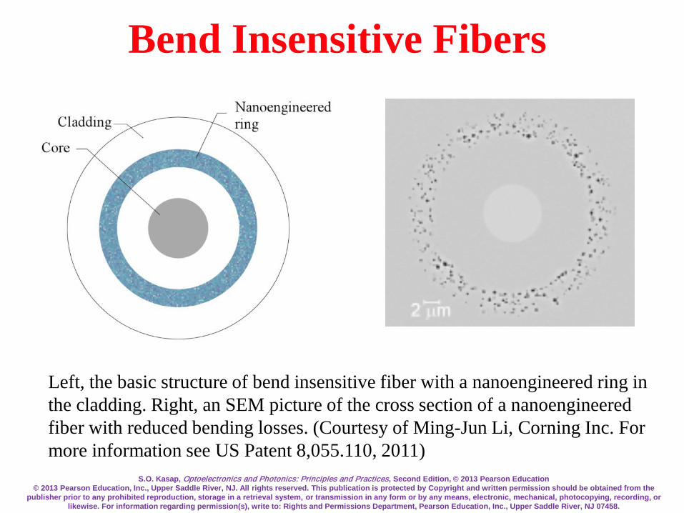
S.O. Kasap, Optoelectronics and Photonics: Principles and Practices, Second Edition, © 2013 Pearson Education© 2013 Pearson Education, Inc., Upper Saddle River, NJ. All rights reserved. This publication is protected by Copyright and written permission should be obtained from the
publisher prior to any prohibited reproduction, storage in a retrieval system, or transmission in any form or by any means, electronic, mechanical, photocopying, recording, or likewise. For information regarding permission(s), write to: Rights and Permissions Department, Pearson Education, Inc., Upper Saddle River, NJ 07458.
Bend Insensitive Fibers
Left, the basic structure of bend insensitive fiber with a nanoengineered ring in the cladding. Right, an SEM picture of the cross section of a nanoengineeredfiber with reduced bending losses. (Courtesy of Ming-Jun Li, Corning Inc. For more information see US Patent 8,055.110, 2011)

S.O. Kasap, Optoelectronics and Photonics: Principles and Practices, Second Edition, © 2013 Pearson Education© 2013 Pearson Education, Inc., Upper Saddle River, NJ. All rights reserved. This publication is protected by Copyright and written permission should be obtained from the
publisher prior to any prohibited reproduction, storage in a retrieval system, or transmission in any form or by any means, electronic, mechanical, photocopying, recording, or likewise. For information regarding permission(s), write to: Rights and Permissions Department, Pearson Education, Inc., Upper Saddle River, NJ 07458.
Bending Loss in FibersGeneral Description
αB = Aexp(−R/Rc)
A and Rc are constants

S.O. Kasap, Optoelectronics and Photonics: Principles and Practices, Second Edition, © 2013 Pearson Education© 2013 Pearson Education, Inc., Upper Saddle River, NJ. All rights reserved. This publication is protected by Copyright and written permission should be obtained from the
publisher prior to any prohibited reproduction, storage in a retrieval system, or transmission in any form or by any means, electronic, mechanical, photocopying, recording, or likewise. For information regarding permission(s), write to: Rights and Permissions Department, Pearson Education, Inc., Upper Saddle River, NJ 07458.
Bending Loss αB = Aexp(−R/Rc)where A and Rc are constants
For single mode fibers, a quantity called a MAC-value, or a MAC-number, NMAC, has been used to characterize the bending loss. NMACis defined by
c
Nλ
MFDh wavelengtoff-Cut
diameter fieldModeMAC ==

S.O. Kasap, Optoelectronics and Photonics: Principles and Practices, Second Edition, © 2013 Pearson Education© 2013 Pearson Education, Inc., Upper Saddle River, NJ. All rights reserved. This publication is protected by Copyright and written permission should be obtained from the
publisher prior to any prohibited reproduction, storage in a retrieval system, or transmission in any form or by any means, electronic, mechanical, photocopying, recording, or likewise. For information regarding permission(s), write to: Rights and Permissions Department, Pearson Education, Inc., Upper Saddle River, NJ 07458.
∆−∝
−∝ − 2/3expexp R
RR
c
α
Microbending Loss
Measured microbending loss for a 10 cm fiber bent by different amounts of radius of curvature R. Single mode fiber with a core diameter of 3.9 µm, cladding radius 48 µm, ∆ = 0.00275, NA ≈ 0.10, V ≈ 1.67 and 2.08. Data extracted from A.J. Harris and P.F. Castle, "Bend Loss Measurements on High Aperture Single-Mode Fibers as a Function of Wavelength and Bend Radius", IEEE J. Light Wave Technology, Vol. LT14, 34, 1986, and repotted with a smoothed curve; see original article for the discussion of peaks in αB vs. R at 790 nm).

S.O. Kasap, Optoelectronics and Photonics: Principles and Practices, Second Edition, © 2013 Pearson Education© 2013 Pearson Education, Inc., Upper Saddle River, NJ. All rights reserved. This publication is protected by Copyright and written permission should be obtained from the
publisher prior to any prohibited reproduction, storage in a retrieval system, or transmission in any form or by any means, electronic, mechanical, photocopying, recording, or likewise. For information regarding permission(s), write to: Rights and Permissions Department, Pearson Education, Inc., Upper Saddle River, NJ 07458.
Bending Loss in SMFαB = Aexp(−R/Rc)
MAC-value, or a MAC-number, NMAC
c
Nλ
MFDh wavelengtoff-Cut
diameter fieldModeMAC ==
NOTESαB increases with increasing MFDαB decreasing cut-off wavelength. αB increases exponentially with the MAC-numberIt is not a universal function, and different types of fibers, with very different refractive index profiles, can exhibit different αB−NMAC behavior.
NMAC values are typically in the range 6 − 8

S.O. Kasap, Optoelectronics and Photonics: Principles and Practices, Second Edition, © 2013 Pearson Education© 2013 Pearson Education, Inc., Upper Saddle River, NJ. All rights reserved. This publication is protected by Copyright and written permission should be obtained from the
publisher prior to any prohibited reproduction, storage in a retrieval system, or transmission in any form or by any means, electronic, mechanical, photocopying, recording, or likewise. For information regarding permission(s), write to: Rights and Permissions Department, Pearson Education, Inc., Upper Saddle River, NJ 07458.
Standard Fibers and Bending Loss
αB = Aexp(−R/Rc)
OM1 MMF for use at 850 and 1310
OM1 “Maximum bending (macrobending) loss of 0.5 dB when the fiber is wound 100 turns with a radius 75 mm i.e. a bending loss of 0.005 dB/turn for a bend radius
of 75 mm.”
Bend insensitive fibers have been designed to have lower bend losses. For example, some fiber manufacturers specify the allowed bend radius for a given
level of attenuation at a certain wavelength (e.g. 1310 nm)

S.O. Kasap, Optoelectronics and Photonics: Principles and Practices, Second Edition, © 2013 Pearson Education© 2013 Pearson Education, Inc., Upper Saddle River, NJ. All rights reserved. This publication is protected by Copyright and written permission should be obtained from the
publisher prior to any prohibited reproduction, storage in a retrieval system, or transmission in any form or by any means, electronic, mechanical, photocopying, recording, or likewise. For information regarding permission(s), write to: Rights and Permissions Department, Pearson Education, Inc., Upper Saddle River, NJ 07458.
Example: Experiments on a standard SMF operating around 1550 nm have shown that thebending loss is 0.124 dB/turn when the bend radius is 12.5 mm and 15.0 dB/turn when the bendradius is 5.0 mm. What is the loss at a bend radius of 10 mm?
Bending Loss Example
SolutionApply
αB = Aexp(−R/Rc)0.124 dB/turn = Aexp[−(12.5 mm)/Rc]15.0 dB/turn = Aexp[−(5.0 mm)/Rc]
Solve for A and Rc. Dividing the first by the second and separating out Rc we find,
Rc = (12.5 mm − 5.0 mm) / ln(15.0/0.124) = 1.56 mmand A = (15.0 dB/turn) exp[(5.0 mm)/(1.56 mm] = 370 dB/turn
At R = 10 mmαB = Aexp(−R/Rc) = (370)exp[−(10 mm)/(1.56 mm)]
= 0.61 dB/turn.The experimental value is also 0.61 dB/turn to within two decimals.
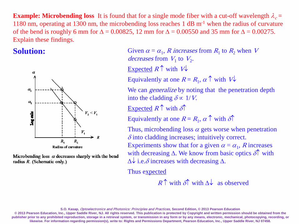
S.O. Kasap, Optoelectronics and Photonics: Principles and Practices, Second Edition, © 2013 Pearson Education© 2013 Pearson Education, Inc., Upper Saddle River, NJ. All rights reserved. This publication is protected by Copyright and written permission should be obtained from the
publisher prior to any prohibited reproduction, storage in a retrieval system, or transmission in any form or by any means, electronic, mechanical, photocopying, recording, or likewise. For information regarding permission(s), write to: Rights and Permissions Department, Pearson Education, Inc., Upper Saddle River, NJ 07458.
Example: Microbending loss It is found that for a single mode fiber with a cut-off wavelength λc = 1180 nm, operating at 1300 nm, the microbending loss reaches 1 dB m-1 when the radius of curvature of the bend is roughly 6 mm for ∆ = 0.00825, 12 mm for ∆ = 0.00550 and 35 mm for ∆ = 0.00275. Explain these findings.
Solution: Given α = α1, R increases from R1 to R2 when Vdecreases from V1 to V2. Expected R ↑ with V↓
Equivalently at one R = R1, α ↑ with V↓
We can generalize by noting that the penetration depth into the cladding δ ∝ 1/V.Expected R ↑ with δ↑
Equivalently at one R = R1, α ↑ with δ↑
Thus, microbending loss α gets worse when penetration δ into cladding increases; intuitively correct. Experiments show that for a given α = α1, R increases with decreasing ∆. We know from basic optics δ↑ with ∆↓ i.e.δ increases with decreasing ∆. Thus expected
R ↑ with δ↑ with ∆↓ as observed

S.O. Kasap, Optoelectronics and Photonics: Principles and Practices, Second Edition, © 2013 Pearson Education© 2013 Pearson Education, Inc., Upper Saddle River, NJ. All rights reserved. This publication is protected by Copyright and written permission should be obtained from the
publisher prior to any prohibited reproduction, storage in a retrieval system, or transmission in any form or by any means, electronic, mechanical, photocopying, recording, or likewise. For information regarding permission(s), write to: Rights and Permissions Department, Pearson Education, Inc., Upper Saddle River, NJ 07458.
Example: Microbending loss It is found that for a single mode fiber with a cut-off wavelength λc = 1180 nm, operating at 1300 nm, the microbending loss reaches 1 dB m-1 when the radius of curvature of the bend is roughly 6 mm for ∆ = 0.00825, 12 mm for ∆ = 0.00550 and 35 mm for ∆ = 0.00275. Explain these findings.
Solution:
Log-log plot of the results ofexperiments on ∆ vs. bendradius R for 1 dB/mmicrobending loss
♦
♦
♦0.002
0.01
1 10 100Bend radius (mm)
∆ x = -0.62
α ∝exp −RRc
∝exp −
R∆−3/ 2
Rc is a constant (“a critical radius type of constant”) that is proportional to ∆−3/2. Taking logs,lnα = −∆3/2R + constantWe are interested in the ∆ vs R behavior at a constant α. We can lump the constant into lnα and obtain,∆∝ R-2/3
The plot in the figure gives an index close this value.

S.O. Kasap, Optoelectronics and Photonics: Principles and Practices, Second Edition, © 2013 Pearson Education© 2013 Pearson Education, Inc., Upper Saddle River, NJ. All rights reserved. This publication is protected by Copyright and written permission should be obtained from the
publisher prior to any prohibited reproduction, storage in a retrieval system, or transmission in any form or by any means, electronic, mechanical, photocopying, recording, or likewise. For information regarding permission(s), write to: Rights and Permissions Department, Pearson Education, Inc., Upper Saddle River, NJ 07458.
Manufacture of Optical Fibers

S.O. Kasap, Optoelectronics and Photonics: Principles and Practices, Second Edition, © 2013 Pearson Education© 2013 Pearson Education, Inc., Upper Saddle River, NJ. All rights reserved. This publication is protected by Copyright and written permission should be obtained from the
publisher prior to any prohibited reproduction, storage in a retrieval system, or transmission in any form or by any means, electronic, mechanical, photocopying, recording, or likewise. For information regarding permission(s), write to: Rights and Permissions Department, Pearson Education, Inc., Upper Saddle River, NJ 07458.
The cross section of a typical single-mode fiber with a tight buffer tube. (d = diameter)
Typical Cross Section of an Optical Fiber

S.O. Kasap, Optoelectronics and Photonics: Principles and Practices, Second Edition, © 2013 Pearson Education© 2013 Pearson Education, Inc., Upper Saddle River, NJ. All rights reserved. This publication is protected by Copyright and written permission should be obtained from the
publisher prior to any prohibited reproduction, storage in a retrieval system, or transmission in any form or by any means, electronic, mechanical, photocopying, recording, or likewise. For information regarding permission(s), write to: Rights and Permissions Department, Pearson Education, Inc., Upper Saddle River, NJ 07458.
Outside vapor Deposition (OVD)
Main reactions are
Silicon tetrachloride and oxygen produces silica
SiCl4(gas) + O2(gas) → SiO2(solid) + 2Cl2(gas)
Germanium tetrachloride and oxygen produces germania
GeCl4(gas) + O2(gas) → GeO2(solid) + 2Cl2(gas)

S.O. Kasap, Optoelectronics and Photonics: Principles and Practices, Second Edition, © 2013 Pearson Education© 2013 Pearson Education, Inc., Upper Saddle River, NJ. All rights reserved. This publication is protected by Copyright and written permission should be obtained from the
publisher prior to any prohibited reproduction, storage in a retrieval system, or transmission in any form or by any means, electronic, mechanical, photocopying, recording, or likewise. For information regarding permission(s), write to: Rights and Permissions Department, Pearson Education, Inc., Upper Saddle River, NJ 07458.
Donald Keck, Bob Maurer and Peter Schultz (left to right) at Corning shortly afterannouncing the first low loss optical fibers made in 1970. Keck, Maurer andSchultz developed the outside vapor deposition (OVD) method for the fabricationof preforms that are used in drawing fibers with low losses. Their OVD was basedon Franklin Hyde’s vapor deposition process earlier at Corning in 1930s. OVD isstill used today at Corning in manufacturing low loss fibers. (Courtesy of Corning)

S.O. Kasap, Optoelectronics and Photonics: Principles and Practices, Second Edition, © 2013 Pearson Education© 2013 Pearson Education, Inc., Upper Saddle River, NJ. All rights reserved. This publication is protected by Copyright and written permission should be obtained from the
publisher prior to any prohibited reproduction, storage in a retrieval system, or transmission in any form or by any means, electronic, mechanical, photocopying, recording, or likewise. For information regarding permission(s), write to: Rights and Permissions Department, Pearson Education, Inc., Upper Saddle River, NJ 07458.
Peter Schultz making a germania-doped multimode fiber preform using the outside vapor deposition (OVD) process circa 1972 at Corning. Soot is deposited layer by layer on a thin bait rod rotating and translating in front of the flame hydrolysis burner. The first fibers made by the OVD at that time had an attenuation of 4 dB/km, which was among the lowest, and below what Charles Kao thought was needed for optical fiber communications, 20 dB/km (Courtesy of Peter Schultz.)

S.O. Kasap, Optoelectronics and Photonics: Principles and Practices, Second Edition, © 2013 Pearson Education© 2013 Pearson Education, Inc., Upper Saddle River, NJ. All rights reserved. This publication is protected by Copyright and written permission should be obtained from the
publisher prior to any prohibited reproduction, storage in a retrieval system, or transmission in any form or by any means, electronic, mechanical, photocopying, recording, or likewise. For information regarding permission(s), write to: Rights and Permissions Department, Pearson Education, Inc., Upper Saddle River, NJ 07458.
Outside Vapor Deposition (OVD)
Schematic illustration of OVD and the preform preparation for fiber drawing. (a)Reaction of gases in the burner flame produces glass soot that deposits on to the outsidesurface of the mandrel. (b) The mandrel is removed and the hollow porous soot preformis consolidated; the soot particles are sintered, fused, together to form a clear glass rod.(c) The consolidated glass rod is used as a preform in fiber drawing.

S.O. Kasap, Optoelectronics and Photonics: Principles and Practices, Second Edition, © 2013 Pearson Education© 2013 Pearson Education, Inc., Upper Saddle River, NJ. All rights reserved. This publication is protected by Copyright and written permission should be obtained from the
publisher prior to any prohibited reproduction, storage in a retrieval system, or transmission in any form or by any means, electronic, mechanical, photocopying, recording, or likewise. For information regarding permission(s), write to: Rights and Permissions Department, Pearson Education, Inc., Upper Saddle River, NJ 07458.
WAVELENGTH DIVISION MULTIPLEXING: WDM
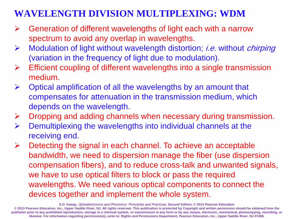
S.O. Kasap, Optoelectronics and Photonics: Principles and Practices, Second Edition, © 2013 Pearson Education© 2013 Pearson Education, Inc., Upper Saddle River, NJ. All rights reserved. This publication is protected by Copyright and written permission should be obtained from the
publisher prior to any prohibited reproduction, storage in a retrieval system, or transmission in any form or by any means, electronic, mechanical, photocopying, recording, or likewise. For information regarding permission(s), write to: Rights and Permissions Department, Pearson Education, Inc., Upper Saddle River, NJ 07458.
WAVELENGTH DIVISION MULTIPLEXING: WDM Generation of different wavelengths of light each with a narrow
spectrum to avoid any overlap in wavelengths. Modulation of light without wavelength distortion; i.e. without chirping
(variation in the frequency of light due to modulation). Efficient coupling of different wavelengths into a single transmission
medium. Optical amplification of all the wavelengths by an amount that
compensates for attenuation in the transmission medium, which depends on the wavelength.
Dropping and adding channels when necessary during transmission. Demultiplexing the wavelengths into individual channels at the
receiving end. Detecting the signal in each channel. To achieve an acceptable
bandwidth, we need to dispersion manage the fiber (use dispersion compensation fibers), and to reduce cross-talk and unwanted signals, we have to use optical filters to block or pass the required wavelengths. We need various optical components to connect the devices together and implement the whole system.

S.O. Kasap, Optoelectronics and Photonics: Principles and Practices, Second Edition, © 2013 Pearson Education© 2013 Pearson Education, Inc., Upper Saddle River, NJ. All rights reserved. This publication is protected by Copyright and written permission should be obtained from the
publisher prior to any prohibited reproduction, storage in a retrieval system, or transmission in any form or by any means, electronic, mechanical, photocopying, recording, or likewise. For information regarding permission(s), write to: Rights and Permissions Department, Pearson Education, Inc., Upper Saddle River, NJ 07458.
WAVELENGTH DIVISION MULTIPLEXING: WDM
If ∆υ < 200 GHz then WDM is called DENSE WAVELENGTH DIVISIONMULTIPLEXING and denoted as DWDM.
At present, DWDM stands typically at 100 GHz separated channels which is equivalent to a wavelength separation of 0.8 nm.
DWDM imposes stringent requirements on lasers and modulators used for generating the optical signals.
It is not possible to tolerate even slight shifts in the optical signal frequency when channels are spaced closely. As the channel spacing becomes narrower as in DWDM, one also encounters various other problems not previously present. For example, any nonlinearity in a component carrying the channels can produce intermodulation between the channels; an undesirable effect. Thus, the total optical power must be kept below the onset of nonlinearity in the fiber and optical amplifiers within the WDM system.

S.O. Kasap, Optoelectronics and Photonics: Principles and Practices, Second Edition, © 2013 Pearson Education© 2013 Pearson Education, Inc., Upper Saddle River, NJ. All rights reserved. This publication is protected by Copyright and written permission should be obtained from the
publisher prior to any prohibited reproduction, storage in a retrieval system, or transmission in any form or by any means, electronic, mechanical, photocopying, recording, or likewise. For information regarding permission(s), write to: Rights and Permissions Department, Pearson Education, Inc., Upper Saddle River, NJ 07458.
Nonlinear Effects and DWDM
Induced Polarization, P = a1E + a2E2 + a3E3
P = a1E + a3E3Nonlinear behavior for glasses
Nonlinear effects
Consider signals at 3 channels
E1 = C1cos(2πυ1t) E2 = C2cos(2πυ2t) E3 = C3cos(2πυ3t)
Nonlinear P = a3E3 = a3(E1 + E2 + E3)3
= a3(E13) + …+ 2a3(E1E2E3) +...+ a3(E3
3)
Four photon mixing

S.O. Kasap, Optoelectronics and Photonics: Principles and Practices, Second Edition, © 2013 Pearson Education© 2013 Pearson Education, Inc., Upper Saddle River, NJ. All rights reserved. This publication is protected by Copyright and written permission should be obtained from the
publisher prior to any prohibited reproduction, storage in a retrieval system, or transmission in any form or by any means, electronic, mechanical, photocopying, recording, or likewise. For information regarding permission(s), write to: Rights and Permissions Department, Pearson Education, Inc., Upper Saddle River, NJ 07458.
Nonlinear Effects and DWDM
Nonlinear P = a3(E13) +…+ 2a3(E1E2E3) +...+ a3(E3
3)
Nonlinear P = …+ 2a3C1C2C3cos(2πυ1t)cos(2πυ2t)cos(2πυ3t) +…
Frequencies mix and can be written as sum and difference
frequencies
Consider three optical signals atυ1
υ2 = (υ1 + 100 GHz )
υ3 = (υ2 + 100 GHz ) = (υ1 + 200 GHz)

S.O. Kasap, Optoelectronics and Photonics: Principles and Practices, Second Edition, © 2013 Pearson Education© 2013 Pearson Education, Inc., Upper Saddle River, NJ. All rights reserved. This publication is protected by Copyright and written permission should be obtained from the
publisher prior to any prohibited reproduction, storage in a retrieval system, or transmission in any form or by any means, electronic, mechanical, photocopying, recording, or likewise. For information regarding permission(s), write to: Rights and Permissions Department, Pearson Education, Inc., Upper Saddle River, NJ 07458.
Nonlinear Effects and DWDMFour Photon (Wave) Mixing
Three photons (υ1, υ2, υ3 ) mix to generate a fourth photon (υ4 )
υ4 = υ1 + υ2 − υ3
υ4 = υ1 + ( υ1 + 100 GHz ) − (υ1 + 200 GHz)
υ4 = υ1 − 100 GHz on top of previous channel
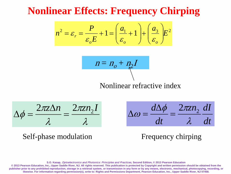
S.O. Kasap, Optoelectronics and Photonics: Principles and Practices, Second Edition, © 2013 Pearson Education© 2013 Pearson Education, Inc., Upper Saddle River, NJ. All rights reserved. This publication is protected by Copyright and written permission should be obtained from the
publisher prior to any prohibited reproduction, storage in a retrieval system, or transmission in any form or by any means, electronic, mechanical, photocopying, recording, or likewise. For information regarding permission(s), write to: Rights and Permissions Department, Pearson Education, Inc., Upper Saddle River, NJ 07458.
Nonlinear Effects: Frequency Chirping
2312 11 EaaE
Pnooo
r
+
+=+==
εεεε
n = no + n2I
Nonlinear refractive index
λπ
λπφ Iznnz 222
=∆
=∆dtdIzn
dtd
λπφω 22
=∆
=∆
Self-phase modulation Frequency chirping

S.O. Kasap, Optoelectronics and Photonics: Principles and Practices, Second Edition, © 2013 Pearson Education© 2013 Pearson Education, Inc., Upper Saddle River, NJ. All rights reserved. This publication is protected by Copyright and written permission should be obtained from the
publisher prior to any prohibited reproduction, storage in a retrieval system, or transmission in any form or by any means, electronic, mechanical, photocopying, recording, or likewise. For information regarding permission(s), write to: Rights and Permissions Department, Pearson Education, Inc., Upper Saddle River, NJ 07458.
Nonlinear Effects: Frequency Chirpingn = no + n2I
λπ
λπφ Iznnz 222
=∆
=∆dtdIzn
dtd
λπφω 22
=∆
=∆
Self-phase modulation Frequency chirping

S.O. Kasap, Optoelectronics and Photonics: Principles and Practices, Second Edition, © 2013 Pearson Education© 2013 Pearson Education, Inc., Upper Saddle River, NJ. All rights reserved. This publication is protected by Copyright and written permission should be obtained from the
publisher prior to any prohibited reproduction, storage in a retrieval system, or transmission in any form or by any means, electronic, mechanical, photocopying, recording, or likewise. For information regarding permission(s), write to: Rights and Permissions Department, Pearson Education, Inc., Upper Saddle River, NJ 07458.
Stimulated Brillouin Scattering
(a) Scattering of a forward travelling EM wave A by an acoustic wave results in a reflected, backscattered, wave B that has a slightly different frequency, by Ω. (b) The forward and
reflected waves, A and B respectively, interfere to give rise to a standing wave that propagates at the acoustic velocity va. As a result of electrostriction, an acoustic wave is
generated that reinforces the original acoustic wave and stimulates further scattering.

S.O. Kasap, Optoelectronics and Photonics: Principles and Practices, Second Edition, © 2013 Pearson Education© 2013 Pearson Education, Inc., Upper Saddle River, NJ. All rights reserved. This publication is protected by Copyright and written permission should be obtained from the
publisher prior to any prohibited reproduction, storage in a retrieval system, or transmission in any form or by any means, electronic, mechanical, photocopying, recording, or likewise. For information regarding permission(s), write to: Rights and Permissions Department, Pearson Education, Inc., Upper Saddle River, NJ 07458.
Stimulated Brillouin Scattering (SBS)
Atomic vibrations give rise to traveling waves in the bulk − phonons. Collective vibrations of the atoms in a solid give rise to lattice waves inside the solid
Acoustic lattice waves in a solid involve periodic strain variations along the direction of propagation.
Changes in the strain result in changes in the refractive index through a phenomenon called the photoelastic effect. (The refractive index depends on strain.) Thus, there is a periodic variation in the refractive index which moves with an acoustic velocity va as depicted
The moving diffraction grating reflects back some of the forward propagating EM wave A to give rise to a back scattered wave B as shown. The frequency ωB of the back scattered wave B is Doppler shifted from that of the forward wave ωA by the frequency Ω of the acoustic wave i.e. ωB = ωA − Ω.

S.O. Kasap, Optoelectronics and Photonics: Principles and Practices, Second Edition, © 2013 Pearson Education© 2013 Pearson Education, Inc., Upper Saddle River, NJ. All rights reserved. This publication is protected by Copyright and written permission should be obtained from the
publisher prior to any prohibited reproduction, storage in a retrieval system, or transmission in any form or by any means, electronic, mechanical, photocopying, recording, or likewise. For information regarding permission(s), write to: Rights and Permissions Department, Pearson Education, Inc., Upper Saddle River, NJ 07458.
Stimulated Brillouin Scattering (SBS)The forward wave A and the back scattered wave B interfere and give rise to a standing wave C.
This standing wave C represents a periodic variation in the field that moves with a velocity va along the direction of the original acoustic wave
The field variation in C produces a periodic displacement of the atoms in the medium, through a phenomenon called electrostriction. (The application of an electric field causes a substance to change shape, i.e. experience strain.). Therefore, a periodic variation in strain develops, which moves at the acoustic velocity va.
The moving strain variation is really an acoustic wave, which reinforces the original acoustic wave and stimulates more back scattering. Thus, it is clear that, a condition can be easily reached that Brillouin scattering stimulates further scattering; stimulated Brillouin scattering (SBS).

S.O. Kasap, Optoelectronics and Photonics: Principles and Practices, Second Edition, © 2013 Pearson Education© 2013 Pearson Education, Inc., Upper Saddle River, NJ. All rights reserved. This publication is protected by Copyright and written permission should be obtained from the
publisher prior to any prohibited reproduction, storage in a retrieval system, or transmission in any form or by any means, electronic, mechanical, photocopying, recording, or likewise. For information regarding permission(s), write to: Rights and Permissions Department, Pearson Education, Inc., Upper Saddle River, NJ 07458.
Stimulated Brillouin Scattering (SBS)The SBS effect increases as the input light power increase
The SBS effect increases as the spectral width of the input light becomes narrower.
The onset of SBS depends not only on the fiber type and core diameter, but also on the spectral width ∆λ of the laser output spectrum.
SBS is enhanced as the laser spectral width ∆λ is narrowed or the duration of light pulse is lengthened.
Typical values: For a directly modulated laser diode emitting at 1550 nm into a single mode fiber, the onset of SBS is expected to occur at power levels greater than 20 − 30 mW. In DWDM systems with externally modulated lasers, i.e. narrower ∆λ, the onset of SBS can be as low as ~10 mW. SBS is an important limiting factor in transmitting high power signals in WDM systems.

S.O. Kasap, Optoelectronics and Photonics: Principles and Practices, Second Edition, © 2013 Pearson Education© 2013 Pearson Education, Inc., Upper Saddle River, NJ. All rights reserved. This publication is protected by Copyright and written permission should be obtained from the
publisher prior to any prohibited reproduction, storage in a retrieval system, or transmission in any form or by any means, electronic, mechanical, photocopying, recording, or likewise. For information regarding permission(s), write to: Rights and Permissions Department, Pearson Education, Inc., Upper Saddle River, NJ 07458.
Bragg Fibers
The high (n1) and low (n2) alternating refractive index profile constitutes a Bragg grating which acts as a dielectric mirror.
There is a band of wavelengths, forming a stop-band, that are not allowed to propagate into the Bragg grating.
We can also view the periodic variation in n as forming a photonic crystal cladding in one-dimension, along the radial direction, with a stop-band, i.e. a photonic bandgap.
Light is bound within the core of the guide for wavelengths within this stop-band. Light can only propagate along z.
d1 = λ/n1 and d2 = λ/n2
Bragg fibers have a core region surrounded by a cladding that is made up of concentrating layers of high low refractive index dielectric media
The core can be a low refractive index solid material or simply hollow. In the latter case, we have a hollow Bragg fiber.
∴ d1n1 = d2n2
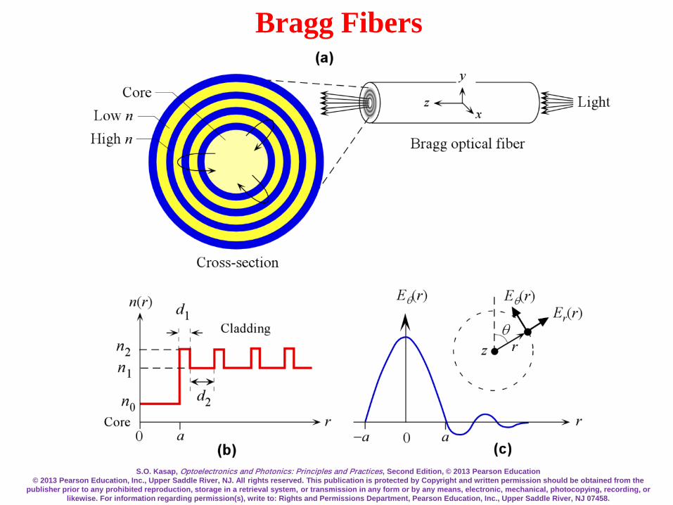
S.O. Kasap, Optoelectronics and Photonics: Principles and Practices, Second Edition, © 2013 Pearson Education© 2013 Pearson Education, Inc., Upper Saddle River, NJ. All rights reserved. This publication is protected by Copyright and written permission should be obtained from the
publisher prior to any prohibited reproduction, storage in a retrieval system, or transmission in any form or by any means, electronic, mechanical, photocopying, recording, or likewise. For information regarding permission(s), write to: Rights and Permissions Department, Pearson Education, Inc., Upper Saddle River, NJ 07458.
Bragg Fibers
(a) A Bragg fiber and its cross section. The Bragg grating in the cladding can be viewed to reflect the waves back into the core over its stop-band. (b) The refractive index variation
(exaggerated). (c) Typical field distribution for the circumferential field Eθ.

S.O. Kasap, Optoelectronics and Photonics: Principles and Practices, Second Edition, © 2013 Pearson Education© 2013 Pearson Education, Inc., Upper Saddle River, NJ. All rights reserved. This publication is protected by Copyright and written permission should be obtained from the
publisher prior to any prohibited reproduction, storage in a retrieval system, or transmission in any form or by any means, electronic, mechanical, photocopying, recording, or likewise. For information regarding permission(s), write to: Rights and Permissions Department, Pearson Education, Inc., Upper Saddle River, NJ 07458.
Photonic Crystal Fibers: Holey Fibers
(a) A solid core PCF. Light is index guided. The cladding has a hexagonal array of holes. d is the hole diameter and Λ is the array pitch, spacing
between the holes (b) and (c) A hollow core PCF. Light is photonic bandgap(PBG) guided.

S.O. Kasap, Optoelectronics and Photonics: Principles and Practices, Second Edition, © 2013 Pearson Education© 2013 Pearson Education, Inc., Upper Saddle River, NJ. All rights reserved. This publication is protected by Copyright and written permission should be obtained from the
publisher prior to any prohibited reproduction, storage in a retrieval system, or transmission in any form or by any means, electronic, mechanical, photocopying, recording, or likewise. For information regarding permission(s), write to: Rights and Permissions Department, Pearson Education, Inc., Upper Saddle River, NJ 07458.
Photonic Crystal Fibers: Holey FibersLeft: The first solid core photonic crystal fiber prepared by Philip Russell and coworkers at the University of Bath in 1996; an endlessly single mode fiber. (Courtesy of Philip Russell)
Left: One of the first hollow core photonic crystal fibers, guiding light by the photonic bandgap effect (1998) (Courtesy of Philip Russell)
Above: A commercially available hollow core photonic crystal fiber from Blaze Photonics. (Courtesy of Philip Russell)

S.O. Kasap, Optoelectronics and Photonics: Principles and Practices, Second Edition, © 2013 Pearson Education© 2013 Pearson Education, Inc., Upper Saddle River, NJ. All rights reserved. This publication is protected by Copyright and written permission should be obtained from the
publisher prior to any prohibited reproduction, storage in a retrieval system, or transmission in any form or by any means, electronic, mechanical, photocopying, recording, or likewise. For information regarding permission(s), write to: Rights and Permissions Department, Pearson Education, Inc., Upper Saddle River, NJ 07458.
Photonic Crystal Fibers: Holey Fibers
Philip Russell (center), currently at the Max Planck Institute for the Science of Light in Erlangen, Germany, led the team of two postdoctoral research fellows, Jonathan Knight (left)
and Tim Birks (right) (both currently professors at the University of Bath in England) that carried out the initial pioneering research on photonic crystal fibers in the 1990s. (See
reviews by P.St.J. Russell, Science, 299, 358, 2003, J. C. Knight, Nature, 424, 847, 2003) (Courtesy of Philip Russell)

S.O. Kasap, Optoelectronics and Photonics: Principles and Practices, Second Edition, © 2013 Pearson Education© 2013 Pearson Education, Inc., Upper Saddle River, NJ. All rights reserved. This publication is protected by Copyright and written permission should be obtained from the
publisher prior to any prohibited reproduction, storage in a retrieval system, or transmission in any form or by any means, electronic, mechanical, photocopying, recording, or likewise. For information regarding permission(s), write to: Rights and Permissions Department, Pearson Education, Inc., Upper Saddle River, NJ 07458.
Solid Core Photonic Crystal Fibers
Both the core and cladding use the same material, usually silica, but the air holes in the cladding result in an effective refractive index that is lower than the solid core region.
The cladding has a lower effective refractive index than the core, and the whole structure then is like a step index fiber.
Total internal reflection then allows the light to be propagated just as in a step index standard silica fiber. Light is index guided.

S.O. Kasap, Optoelectronics and Photonics: Principles and Practices, Second Edition, © 2013 Pearson Education© 2013 Pearson Education, Inc., Upper Saddle River, NJ. All rights reserved. This publication is protected by Copyright and written permission should be obtained from the
publisher prior to any prohibited reproduction, storage in a retrieval system, or transmission in any form or by any means, electronic, mechanical, photocopying, recording, or likewise. For information regarding permission(s), write to: Rights and Permissions Department, Pearson Education, Inc., Upper Saddle River, NJ 07458.
Solid Core Photonic Crystal Fibers
The solid can be pure silica, rather than germania-doped silica, and hence exhibits lower scattering loss.
Single mode propagation can occur over a very large range of wavelengths, almost as if the fiber is endlessly single mode (ESM). The reason is that the PC in the cladding acts as a filter in the transverse direction, which allows the higher modes to escape (leak out) but not the fundamental mode.
(a) The fundamental mode is confined. (b) Higher modes have more nodes and can leak away through the space.

S.O. Kasap, Optoelectronics and Photonics: Principles and Practices, Second Edition, © 2013 Pearson Education© 2013 Pearson Education, Inc., Upper Saddle River, NJ. All rights reserved. This publication is protected by Copyright and written permission should be obtained from the
publisher prior to any prohibited reproduction, storage in a retrieval system, or transmission in any form or by any means, electronic, mechanical, photocopying, recording, or likewise. For information regarding permission(s), write to: Rights and Permissions Department, Pearson Education, Inc., Upper Saddle River, NJ 07458.
Solid Core Photonic Crystal Fibers
ESM operation: The core of a PCF can be made quite large without losing the single mode operation. The refractive index difference can also be made large by having holes in the cladding. Consequently, PCFs can have high numerical apertures and large core areas; thus, more light can be launched into a PCF. Further, the manipulation of the shape and size of the hole, and the type of lattice (and hence the periodicity i.e. the lattice pitch) leads to a much greater control of chromatic dispersion.
(a) The fundamental mode is confined. (b) Higher modes have more nodes and can leak away through the space.

S.O. Kasap, Optoelectronics and Photonics: Principles and Practices, Second Edition, © 2013 Pearson Education© 2013 Pearson Education, Inc., Upper Saddle River, NJ. All rights reserved. This publication is protected by Copyright and written permission should be obtained from the
publisher prior to any prohibited reproduction, storage in a retrieval system, or transmission in any form or by any means, electronic, mechanical, photocopying, recording, or likewise. For information regarding permission(s), write to: Rights and Permissions Department, Pearson Education, Inc., Upper Saddle River, NJ 07458.
Hollow Core Photonic Crystal Fibers: Holey Fibers
Notice that the core has a lower refractive index (it is hollow) so that we cannot rely on total internal reflection (TIR) to explain light propagation.
Light in the transverse direction is reflected back into the core over frequencies within the stop-band, i.e. photonic bandgap (PBG), of the photonic crystal in the cladding. When light is launched from one end of the fiber, it cannot enter the cladding (its frequency is within the stop-band) and is therefore confined within the hollow core. Light is photonic bandgap guided.

S.O. Kasap, Optoelectronics and Photonics: Principles and Practices, Second Edition, © 2013 Pearson Education© 2013 Pearson Education, Inc., Upper Saddle River, NJ. All rights reserved. This publication is protected by Copyright and written permission should be obtained from the
publisher prior to any prohibited reproduction, storage in a retrieval system, or transmission in any form or by any means, electronic, mechanical, photocopying, recording, or likewise. For information regarding permission(s), write to: Rights and Permissions Department, Pearson Education, Inc., Upper Saddle River, NJ 07458.
Hollow Core Photonic Crystal Fibers: Holey Fibers
As recalled by Philip Russell:
"My idea, then, was to trap light in a hollow core by means of a 2D photonic crystal of microscopic air capillaries running along the entire length of a glass fiber. Appropriately designed, this array would support a PBG for incidence from air, preventing the escape of light from a hollow core into the photonic-crystal cladding and avoiding the need for TIR." (P. St.J. Russell, J. Light Wave Technol, 24, 4729, 2006)
The periodic arrangement of the air holes in the cladding creates a photonic bandgap in the transverse direction that confines the light to the hollow core.

S.O. Kasap, Optoelectronics and Photonics: Principles and Practices, Second Edition, © 2013 Pearson Education© 2013 Pearson Education, Inc., Upper Saddle River, NJ. All rights reserved. This publication is protected by Copyright and written permission should be obtained from the
publisher prior to any prohibited reproduction, storage in a retrieval system, or transmission in any form or by any means, electronic, mechanical, photocopying, recording, or likewise. For information regarding permission(s), write to: Rights and Permissions Department, Pearson Education, Inc., Upper Saddle River, NJ 07458.
Hollow Core Photonic Crystal Fibers: Holey Fibers
There are certain distinct advantages
Material dispersion is absent.
The attenuation in principle should be potentially very small since there is no Rayleigh scattering in the core. However, scattering from irregularities in the air-cladding interface, that is, surface roughness, seems to limit the attenuation.
High powers of light can be launched without having nonlinear effects such as stimulated Brillouin scattering limiting the propagation.
There are other distinct advantages that are related to strong nonlinear effects, which are associated with the photonic crystal cladding.
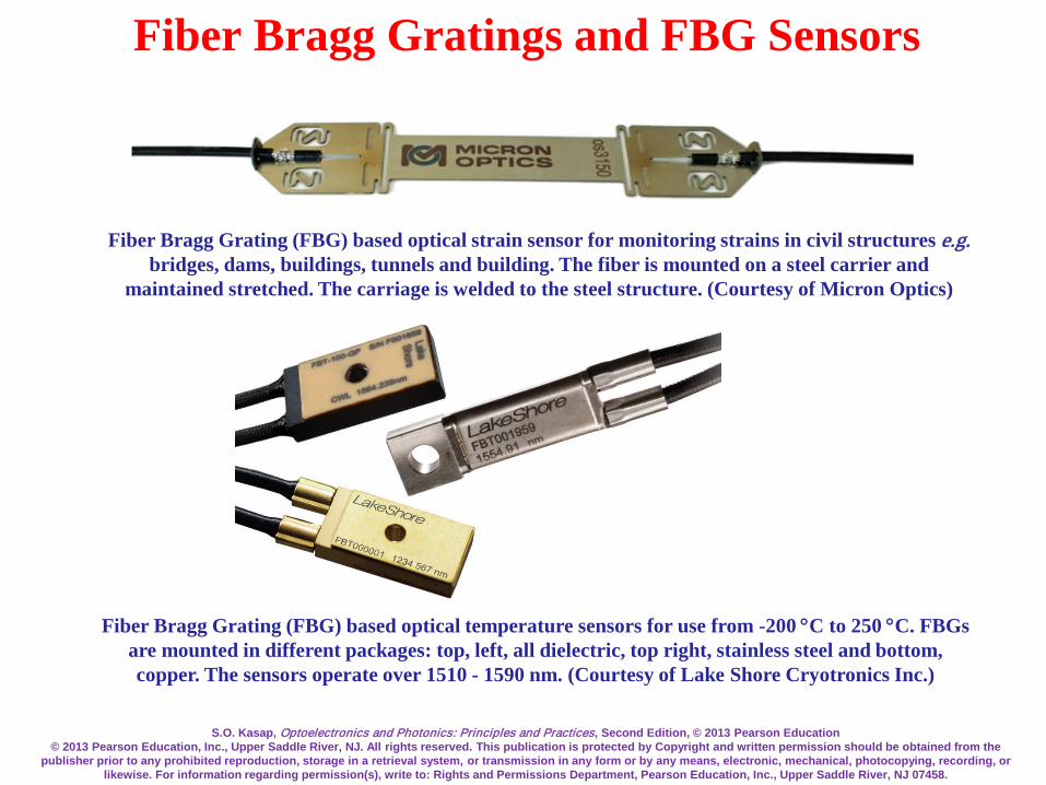
S.O. Kasap, Optoelectronics and Photonics: Principles and Practices, Second Edition, © 2013 Pearson Education© 2013 Pearson Education, Inc., Upper Saddle River, NJ. All rights reserved. This publication is protected by Copyright and written permission should be obtained from the
publisher prior to any prohibited reproduction, storage in a retrieval system, or transmission in any form or by any means, electronic, mechanical, photocopying, recording, or likewise. For information regarding permission(s), write to: Rights and Permissions Department, Pearson Education, Inc., Upper Saddle River, NJ 07458.
Fiber Bragg Gratings and FBG Sensors
Fiber Bragg Grating (FBG) based optical strain sensor for monitoring strains in civil structures e.g.bridges, dams, buildings, tunnels and building. The fiber is mounted on a steel carrier and
maintained stretched. The carriage is welded to the steel structure. (Courtesy of Micron Optics)
Fiber Bragg Grating (FBG) based optical temperature sensors for use from -200 °C to 250 °C. FBGs are mounted in different packages: top, left, all dielectric, top right, stainless steel and bottom, copper. The sensors operate over 1510 - 1590 nm. (Courtesy of Lake Shore Cryotronics Inc.)

S.O. Kasap, Optoelectronics and Photonics: Principles and Practices, Second Edition, © 2013 Pearson Education© 2013 Pearson Education, Inc., Upper Saddle River, NJ. All rights reserved. This publication is protected by Copyright and written permission should be obtained from the
publisher prior to any prohibited reproduction, storage in a retrieval system, or transmission in any form or by any means, electronic, mechanical, photocopying, recording, or likewise. For information regarding permission(s), write to: Rights and Permissions Department, Pearson Education, Inc., Upper Saddle River, NJ 07458.
FBG: Fiber Bragg Grating
Fiber Bragg grating has a Bragg grating written in the core of a singlemode fiber over a certain length of the fiber. The Bragg grating reflects anylight that has the Bragg wavelength λB, which depends on the refractiveindex and the periodicity. The transmitted spectrum has the Braggwavelength missing.

S.O. Kasap, Optoelectronics and Photonics: Principles and Practices, Second Edition, © 2013 Pearson Education© 2013 Pearson Education, Inc., Upper Saddle River, NJ. All rights reserved. This publication is protected by Copyright and written permission should be obtained from the
publisher prior to any prohibited reproduction, storage in a retrieval system, or transmission in any form or by any means, electronic, mechanical, photocopying, recording, or likewise. For information regarding permission(s), write to: Rights and Permissions Department, Pearson Education, Inc., Upper Saddle River, NJ 07458.
Fiber Bragg Grating: FBGVariation in n in the grating acts like a dielectric mirror
Partial Fresnel reflections from the changes in the refractive index add in phase and give rise to a back reflected (back
diffracted) wave only at a certain wavelength λB, called the Bragg wavelength
Λ= nq B 2λ
Integer, 1,2,… normally q = 1 is used, the fundamental

S.O. Kasap, Optoelectronics and Photonics: Principles and Practices, Second Edition, © 2013 Pearson Education© 2013 Pearson Education, Inc., Upper Saddle River, NJ. All rights reserved. This publication is protected by Copyright and written permission should be obtained from the
publisher prior to any prohibited reproduction, storage in a retrieval system, or transmission in any form or by any means, electronic, mechanical, photocopying, recording, or likewise. For information regarding permission(s), write to: Rights and Permissions Department, Pearson Education, Inc., Upper Saddle River, NJ 07458.
Bragg Wavelength λB
)2(2 πqkAB =Λ=∆Φ
A
B
Λ Repeat unit = unit cellFor reflection A and B must be in phase i.e. phase difference should be q2π. This will be so at wavelength λB, the Bragg wavelength. The phase difference between A and B is ∆ΦAB
A and Bare
reflected waves
B
nkλπ2wavevectorAverage ==
Average index in unit cell
Λ= nq B 2λ

S.O. Kasap, Optoelectronics and Photonics: Principles and Practices, Second Edition, © 2013 Pearson Education© 2013 Pearson Education, Inc., Upper Saddle River, NJ. All rights reserved. This publication is protected by Copyright and written permission should be obtained from the
publisher prior to any prohibited reproduction, storage in a retrieval system, or transmission in any form or by any means, electronic, mechanical, photocopying, recording, or likewise. For information regarding permission(s), write to: Rights and Permissions Department, Pearson Education, Inc., Upper Saddle River, NJ 07458.
Fiber Bragg Grating: FBG
)(tanh2 LR κ=
λπκ n∆
=
LnB2
weakλλ =∆
nB
πκλλ
2
strong4
=∆
κL < 1 Weak
kL > 1 Strong
Reflectance, R

S.O. Kasap, Optoelectronics and Photonics: Principles and Practices, Second Edition, © 2013 Pearson Education© 2013 Pearson Education, Inc., Upper Saddle River, NJ. All rights reserved. This publication is protected by Copyright and written permission should be obtained from the
publisher prior to any prohibited reproduction, storage in a retrieval system, or transmission in any form or by any means, electronic, mechanical, photocopying, recording, or likewise. For information regarding permission(s), write to: Rights and Permissions Department, Pearson Education, Inc., Upper Saddle River, NJ 07458.
FBG Sensors
Λ+Λ= δδδλ nnB 22
TLB
B δααλ
δλ )( TCRI +=
εδ epnn 321−=
Photoelastic or elasto-optic coefficient
Strain

S.O. Kasap, Optoelectronics and Photonics: Principles and Practices, Second Edition, © 2013 Pearson Education© 2013 Pearson Education, Inc., Upper Saddle River, NJ. All rights reserved. This publication is protected by Copyright and written permission should be obtained from the
publisher prior to any prohibited reproduction, storage in a retrieval system, or transmission in any form or by any means, electronic, mechanical, photocopying, recording, or likewise. For information regarding permission(s), write to: Rights and Permissions Department, Pearson Education, Inc., Upper Saddle River, NJ 07458.
FBG Sensors
Λ+Λ= δδδλ nnB 22

S.O. Kasap, Optoelectronics and Photonics: Principles and Practices, Second Edition, © 2013 Pearson Education© 2013 Pearson Education, Inc., Upper Saddle River, NJ. All rights reserved. This publication is protected by Copyright and written permission should be obtained from the
publisher prior to any prohibited reproduction, storage in a retrieval system, or transmission in any form or by any means, electronic, mechanical, photocopying, recording, or likewise. For information regarding permission(s), write to: Rights and Permissions Department, Pearson Education, Inc., Upper Saddle River, NJ 07458.
FBG Sensors
A highly simplified schematic diagram of a multiplexed Bragg grating based sensing system. The FBG sensors are distributed on a single fiber that is embedded in the structure in which strains are
to be monitored. The coupler allows optical power to be coupled from one fiber to the other.

S.O. Kasap, Optoelectronics and Photonics: Principles and Practices, Second Edition, © 2013 Pearson Education© 2013 Pearson Education, Inc., Upper Saddle River, NJ. All rights reserved. This publication is protected by Copyright and written permission should be obtained from the
publisher prior to any prohibited reproduction, storage in a retrieval system, or transmission in any form or by any means, electronic, mechanical, photocopying, recording, or likewise. For information regarding permission(s), write to: Rights and Permissions Department, Pearson Education, Inc., Upper Saddle River, NJ 07458.
FBG at 1550 nm

S.O. Kasap, Optoelectronics and Photonics: Principles and Practices, Second Edition, © 2013 Pearson Education© 2013 Pearson Education, Inc., Upper Saddle River, NJ. All rights reserved. This publication is protected by Copyright and written permission should be obtained from the
publisher prior to any prohibited reproduction, storage in a retrieval system, or transmission in any form or by any means, electronic, mechanical, photocopying, recording, or likewise. For information regarding permission(s), write to: Rights and Permissions Department, Pearson Education, Inc., Upper Saddle River, NJ 07458.
Updates andCorrected Slides
Class Demonstrations
Class Problems
Check author’s websitehttp://optoelectronics.usask.ca
Email errors and corrections to [email protected]