Embed Size (px)
Citation preview
Photon-detecting
superconducting resonators
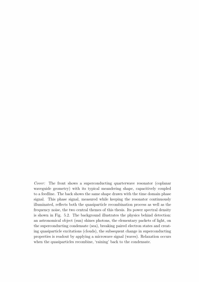
Cover: The front shows a superconducting quarterwave resonator (coplanar
waveguide geometry) with its typical meandering shape, capacitively coupled
to a feedline. The back shows the same shape drawn with the time domain phase
signal. This phase signal, measured while keeping the resonator continuously
illuminated, reflects both the quasiparticle recombination process as well as the
frequency noise, the two central themes of this thesis. Its power spectral density
is shown in Fig. 5.2. The background illustrates the physics behind detection:
an astronomical object (sun) shines photons, the elementary packets of light, on
the superconducting condensate (sea), breaking paired electron states and creat-
ing quasiparticle excitations (clouds), the subsequent change in superconducting
properties is readout by applying a microwave signal (waves). Relaxation occurs
when the quasiparticles recombine, ‘raining’ back to the condensate.
Photon-detecting
superconducting resonators
Proefschrift
ter verkrijging van de graad van doctor
aan de Technische Universiteit Delft,
op gezag van de Rector Magnificus prof. dr. ir. J. T. Fokkema,
voorzitter van het College voor Promoties,
in het openbaar te verdedigen op woensdag 17 juni 2009 om 10:00 uur
door
Rami BARENDS
natuurkundig ingenieur
geboren te Delft.
Dit proefschrift is goedgekeurd door de promotor:
Prof. dr. ir. T. M. Klapwijk
Copromotor:
Dr. J. R. Gao
Samenstelling van de promotiecommissie:
Rector Magnificus, voorzitter
Prof. dr. ir. T. M. Klapwijk Technische Universiteit Delft, promotor
Dr. J. R. Gao Technische Universiteit Delft, copromotor
Prof. dr. ir. J. E. Mooij Technische Universiteit Delft
Prof. dr. P. C. M. Planken Technische Universiteit Delft
Prof. dr. S. Withington University of Cambridge, United Kingdom
Dr. ir. J. J. A. Baselmans SRON Netherlands Institute for Space Research
Dr. A. Neto Nederlandse organisatie voor toegepast-
natuurwetenschappelijk onderzoek (TNO)
Prof. dr. ir. L. M. K. Vandersypen Technische Universiteit Delft, reservelid
Published by: R. Barends
Printed by: GVO printers & designers | Ponsen & Looijen, Ede, The Netherlands
An electronic version of this thesis is available at:
http://repository.tudelft.nl
Copyright c© 2009 by R. Barends. All rights reserved.
Casimir PhD Series, Delft-Leiden, 2009-04
ISBN 978-90-8593-052-5
Contents
1 An eye for the sky 1
1.1 Written in the stars . . . . . . . . . . . . . . . . . . . . . . . . . . 2
1.2 A camera for the cool cosmos . . . . . . . . . . . . . . . . . . . . 4
1.2.1 Challenges for far-infrared detectors . . . . . . . . . . . . . 4
1.2.2 Superconducting detectors . . . . . . . . . . . . . . . . . . 5
1.2.3 Catching cold photons with superconducting resonators . . 6
1.3 Matchmaking on a nanoscale . . . . . . . . . . . . . . . . . . . . . 9
1.4 This thesis . . . . . . . . . . . . . . . . . . . . . . . . . . . . . . . 10
References . . . . . . . . . . . . . . . . . . . . . . . . . . . . . . . 12
2 Relaxation, fluctuation and the response to radiation 15
2.1 Cooper pairs and quasiparticle excitations . . . . . . . . . . . . . 16
2.2 Inelastic interaction at millikelvin temperatures . . . . . . . . . . 19
2.2.1 Scattering in the normal state . . . . . . . . . . . . . . . 19
2.2.2 Quasiparticle recombination in superconducting films . . . 22
2.2.3 Magnetic impurities in superconductors . . . . . . . . . . 27
2.3 Low frequency noise in superconducting systems . . . . . . . . . . 30
2.3.1 Power spectral density . . . . . . . . . . . . . . . . . . . . 31
2.3.2 Particle number fluctuations . . . . . . . . . . . . . . . . . 31
2.3.3 Flux noise . . . . . . . . . . . . . . . . . . . . . . . . . . . 33
2.3.4 Dipole fluctuators . . . . . . . . . . . . . . . . . . . . . . . 34
2.3.5 Noise and frequency deviations in superconducting resonators 35
2.4 High frequency response of a superconducting film . . . . . . . . . 37
References . . . . . . . . . . . . . . . . . . . . . . . . . . . . . . . 41
3 Superconducting resonators 49
3.1 Introduction . . . . . . . . . . . . . . . . . . . . . . . . . . . . . . 50
3.2 Design of a quarterwave resonator . . . . . . . . . . . . . . . . . . 50
3.2.1 A coplanar waveguide transmission line resonator . . . . . 50
3.2.2 Coupling . . . . . . . . . . . . . . . . . . . . . . . . . . . . 54
v
vi Contents
3.3 Microwave perspective on a superconducting resonator . . . . . . 55
3.3.1 Scattering parameters . . . . . . . . . . . . . . . . . . . . 55
3.3.2 Phase, amplitude and the resonance circle . . . . . . . . . 57
3.3.3 Probing signal power . . . . . . . . . . . . . . . . . . . . . 59
3.4 Sample fabrication . . . . . . . . . . . . . . . . . . . . . . . . . . 60
3.5 Measurement techniques . . . . . . . . . . . . . . . . . . . . . . . 61
3.5.1 Cryostat . . . . . . . . . . . . . . . . . . . . . . . . . . . . 61
3.5.2 RF setup . . . . . . . . . . . . . . . . . . . . . . . . . . . 64
3.5.3 Quadrature mixing . . . . . . . . . . . . . . . . . . . . . . 66
3.5.4 Setup noise analysis . . . . . . . . . . . . . . . . . . . . . . 68
References . . . . . . . . . . . . . . . . . . . . . . . . . . . . . . . 72
4 Niobium and tantalum high-Q resonators for photon detectors 75
4.1 Introduction . . . . . . . . . . . . . . . . . . . . . . . . . . . . . . 76
4.2 Experiment . . . . . . . . . . . . . . . . . . . . . . . . . . . . . . 76
4.3 Results . . . . . . . . . . . . . . . . . . . . . . . . . . . . . . . . . 79
4.4 Discussion . . . . . . . . . . . . . . . . . . . . . . . . . . . . . . . 81
4.5 Conclusions . . . . . . . . . . . . . . . . . . . . . . . . . . . . . . 83
References . . . . . . . . . . . . . . . . . . . . . . . . . . . . . . . 84
5 Quasiparticle relaxation in optically excited high-Q supercon-
ducting resonators 87
5.1 Introduction . . . . . . . . . . . . . . . . . . . . . . . . . . . . . . 88
5.2 Probing quasiparticle relaxation with the complex conductivity . . 88
5.3 Relaxation in the frequency domain . . . . . . . . . . . . . . . . . 91
5.4 Low temperature saturation of relaxation . . . . . . . . . . . . . . 93
5.5 Discussion . . . . . . . . . . . . . . . . . . . . . . . . . . . . . . . 94
References . . . . . . . . . . . . . . . . . . . . . . . . . . . . . . . 95
6 Enhancement of quasiparticle recombination in Ta and Al super-
conductors by implantation of magnetic and nonmagnetic atoms 99
6.1 Introduction . . . . . . . . . . . . . . . . . . . . . . . . . . . . . . 100
6.2 Ta and Al superconducting resonators . . . . . . . . . . . . . . . 100
6.3 Enhancement of low temperature recombination . . . . . . . . . . 102
6.4 Conventional pair breaking and pair weakening theory . . . . . . 105
6.5 The role of disorder . . . . . . . . . . . . . . . . . . . . . . . . . . 107
References . . . . . . . . . . . . . . . . . . . . . . . . . . . . . . . 108
Contents vii
7 Contribution of dielectrics to frequency and noise of NbTiN su-
perconducting resonators 111
7.1 NbTiN superconducting resonators for probing dielectrics . . . . . 112
7.2 Contribution of dielectrics to frequency and noise . . . . . . . . . 114
References . . . . . . . . . . . . . . . . . . . . . . . . . . . . . . . 117
8 Noise in NbTiN, Al and Ta superconducting resonators on silicon
and sapphire substrates 121
8.1 Introduction . . . . . . . . . . . . . . . . . . . . . . . . . . . . . . 122
8.2 Contribution of dielectric coverage . . . . . . . . . . . . . . . . . . 122
8.3 Experiment . . . . . . . . . . . . . . . . . . . . . . . . . . . . . . 125
8.4 Noise width dependence . . . . . . . . . . . . . . . . . . . . . . . 126
8.5 Contribution of substrate . . . . . . . . . . . . . . . . . . . . . . . 128
8.6 Discussion and conclusion . . . . . . . . . . . . . . . . . . . . . . 131
References . . . . . . . . . . . . . . . . . . . . . . . . . . . . . . . 131
A Noise equivalent power 135
B Analytical expression for the complex conductivity 137
References . . . . . . . . . . . . . . . . . . . . . . . . . . . . . . . 139
C Noise under continuous illumination 141
Summary 145
Samenvatting 149
Curriculum Vitae 153
List of publications 155
The thought had crossed my mind 159
viii Contents
Chapter 1
An eye for the sky
1
2 Chapter 1. An eye for the sky
1.1 Written in the stars
“It’s written in the stars” is a saying frequently used in relation to foretelling.
Remarkably, the same is actually even more true for the past. Not only because
the photons, the elementary packets of light, have travelled an eternity to arrive;
but also as detecting these photons helps us to understand the formation of stars
and planets, the origins of galaxies, and the Big Bang. Since the Big Bang
about 98 % of the photons released and half of the luminosity of the universe
are observable in the far-infrared range [1], in a frequency ranging from 0.1-10
THz. This frequency range allows us to observe star and planetary formation
which occurs deep within interstellar gas and dust clouds: while the optical light
is scattered and absorbed, the absorbed energy is re-emitted in the far-infrared.
The far-infrared also houses the emissions from cold objects such as planets, the
light from distant galaxies with a high redshift, as well as a snapshot of the very
infant universe.
This snapshot is the cosmic microwave background radiation which formed
when the early universe became transparent; it is the lingering echo of the Big
Bang which has faded to a background radiation temperature of only 2.7 K above
absolute zero. Yet it carries the imprints of tiny fluctuations in the density of
matter and energy at the time of its creation. These variations reveal a great
deal about the universe; such as the accelerating inflation as well as the large
scale structure, revealing the origin of galaxies and pointing towards the presence
of dark matter and energy [2, 3]. Additionally, the far-infrared is brimming with
many atomic and molecular spectral lines; these ‘spectral fingerprints’ allow for
identifying these substances in interstellar gas clouds and planetary atmospheres.
Moreover, the velocity can be extracted from the Doppler-shifted frequencies of
the spectral lines; additionally, the width of the lines is controlled by the pres-
sure and temperature via pressure broadening and by the internal dynamics via
Doppler broadening. By resolving the spectral lines, organic molecules, the build-
ing blocks of life, have been found in the faraway dustclouds around protostars
where planets form [4].
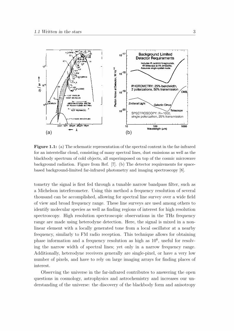
The richness of phenomena observable in the far-infrared range, see Fig. 1.1a,
drives the development of sensitive detectors for large imaging arrays in space-
based observatories as well as earth-based telescopes [5, 6]. Far-infrared imaging
arrays measure the intensity, working in the same manner as many optical digital
cameras in everyday life. This mode of operation is called direct detection, and
comes in two flavours: photometry and spectrophotometry, depending on the
frequency selectivity. Feeding the power over a large frequency range directly to
the imaging array is referred to as photometry. Alternatively, for spectropho-
1.1 Written in the stars 3
(a) (b)
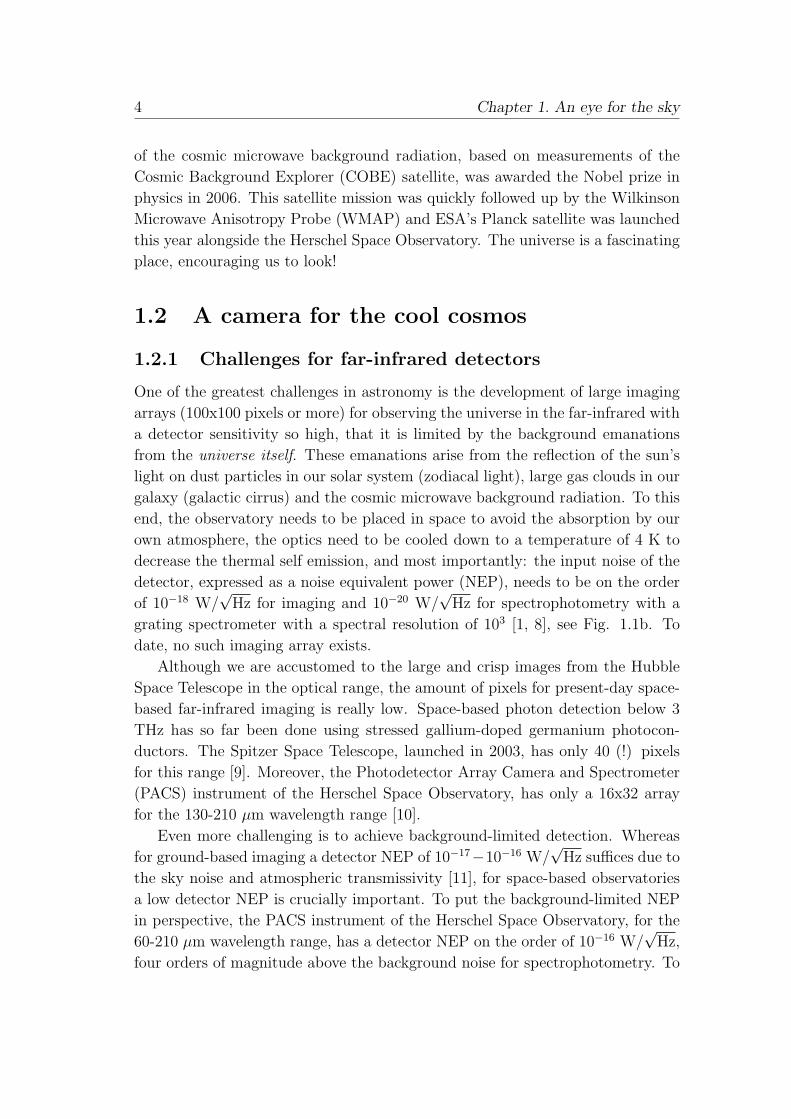
Figure 1.1: (a) The schematic representation of the spectral content in the far-infraredfor an interstellar cloud, consisting of many spectral lines, dust emissions as well as theblackbody spectrum of cold objects, all superimposed on top of the cosmic microwavebackground radiation. Figure from Ref. [7]. (b) The detector requirements for space-based background-limited far-infrared photometry and imaging spectroscopy [8].
tometry the signal is first fed through a tunable narrow bandpass filter, such as
a Michelson interferometer. Using this method a frequency resolution of several
thousand can be accomplished, allowing for spectral line survey over a wide field
of view and broad frequency range. These line surveys are used among others to
identify molecular species as well as finding regions of interest for high resolution
spectroscopy. High resolution spectroscopic observations in the THz frequency
range are made using heterodyne detection. Here, the signal is mixed in a non-
linear element with a locally generated tone from a local oscillator at a nearby
frequency, similarly to FM radio reception. This technique allows for obtaining
phase information and a frequency resolution as high as 106, useful for resolv-
ing the narrow width of spectral lines; yet only in a narrow frequency range.
Additionally, heterodyne receivers generally are single-pixel, or have a very low
number of pixels, and have to rely on large imaging arrays for finding places of
interest.
Observing the universe in the far-infrared contributes to answering the open
questions in cosmology, astrophysics and astrochemistry and increases our un-
derstanding of the universe: the discovery of the blackbody form and anisotropy
4 Chapter 1. An eye for the sky
of the cosmic microwave background radiation, based on measurements of the
Cosmic Background Explorer (COBE) satellite, was awarded the Nobel prize in
physics in 2006. This satellite mission was quickly followed up by the Wilkinson
Microwave Anisotropy Probe (WMAP) and ESA’s Planck satellite was launched
this year alongside the Herschel Space Observatory. The universe is a fascinating
place, encouraging us to look!
1.2 A camera for the cool cosmos
1.2.1 Challenges for far-infrared detectors
One of the greatest challenges in astronomy is the development of large imaging
arrays (100x100 pixels or more) for observing the universe in the far-infrared with
a detector sensitivity so high, that it is limited by the background emanations
from the universe itself. These emanations arise from the reflection of the sun’s
light on dust particles in our solar system (zodiacal light), large gas clouds in our
galaxy (galactic cirrus) and the cosmic microwave background radiation. To this
end, the observatory needs to be placed in space to avoid the absorption by our
own atmosphere, the optics need to be cooled down to a temperature of 4 K to
decrease the thermal self emission, and most importantly: the input noise of the
detector, expressed as a noise equivalent power (NEP), needs to be on the order
of 10−18 W/√
Hz for imaging and 10−20 W/√
Hz for spectrophotometry with a
grating spectrometer with a spectral resolution of 103 [1, 8], see Fig. 1.1b. To
date, no such imaging array exists.
Although we are accustomed to the large and crisp images from the Hubble
Space Telescope in the optical range, the amount of pixels for present-day space-
based far-infrared imaging is really low. Space-based photon detection below 3
THz has so far been done using stressed gallium-doped germanium photocon-
ductors. The Spitzer Space Telescope, launched in 2003, has only 40 (!) pixels
for this range [9]. Moreover, the Photodetector Array Camera and Spectrometer
(PACS) instrument of the Herschel Space Observatory, has only a 16x32 array
for the 130-210 µm wavelength range [10].
Even more challenging is to achieve background-limited detection. Whereas
for ground-based imaging a detector NEP of 10−17−10−16 W/√
Hz suffices due to
the sky noise and atmospheric transmissivity [11], for space-based observatories
a low detector NEP is crucially important. To put the background-limited NEP
in perspective, the PACS instrument of the Herschel Space Observatory, for the
60-210 µm wavelength range, has a detector NEP on the order of 10−16 W/√
Hz,
four orders of magnitude above the background noise for spectrophotometry. To
1.2 A camera for the cool cosmos 5
fully appreciate this difference we need the radiometer equation, which relates the
standard deviation σT to the system input noise temperature TN and observation
time τ : σT = TN/√
Bτ , with B the frequency bandwidth [12]. Thus, to get a
certain signal-to-noise ratio, τ scales with T 2N . In other words, with background-
limited detectors up to a staggering 108 times more observations could be made
than with the PACS instrument in the same mission time! Importantly, very
faint objects can be observed. Obviously, a background-limited imaging array
will revolutionise astronomy.
1.2.2 Superconducting detectors
The development of sensitive far-infrared detectors which can catch these ‘cold’
photons has proven to be elusive. Clearly, the semiconducting technology has
been stretched to its limits with respect to sensitivity and array size. Supercon-
ductors however are ideally suited for the task. The hallmark of superconductors
is that the electrons are condensed in a macroscopic quantum state, formed by
paired electrons - Cooper pairs. This Cooper pair condensate brings about the
characteristic properties such as the zero resistance. The energy needed to break
a pair is 2∆, with ∆ the binding energy, which is on the order of a meV and is
smaller than the energy of a photon in the THz frequency range. Hence these pho-
tons are able to break Cooper pairs into quasiparticle excitations, subsequently
modifying the superconducting properties. Different classes of photon detectors
exist which use different properties. The two main methods are bolometric de-
tection and pair-breaking detection: bolometric detectors monitor the rise of the
temperature of a small superconducting island whereas pair-breaking detectors
effectively count the nonthermal increase in the quasiparticle density and the
related decrease in the Cooper pair density due to incoming radiation.
Transition edge sensor bolometers make use of the steep resistive transition
in a narrow temperature range when the superconducting state collapses at the
critical temperature [13, 14]. By optimally choosing the bath temperature and
bias, a very weak incoming radiation signal can drive the superconductor further
into the superconductor-to-normal transition, bringing about a large change in
resistance. Essentially the transition is used as a highly sensitive thermometer;
yet only in a small temperature range, putting requirements on the dynamic
range in relation to the sensitivity (these requirements are less stringent when
using electro-thermal feedback). The sensitivity is proportional to the thermal
response time. As pixels need to be fast for readout using time domain multiplex-
ing this limits the sensitivity of large arrays. Additionally, each sensor needs its
own superconducting quantum interference detector (SQUID) for readout. Alter-
6 Chapter 1. An eye for the sky
natively, readout can be done in the frequency domain, but this requires coupling
each sensor to a resonator. This complicates large array development.
An example of a pair-breaking detector is a superconducting tunnel junction,
which detects radiation by monitoring the current arising from photo-excited
quasiparticles crossing a very thin insulating oxide barrier [15]. If the barrier is
thin enough, quantum mechanics allows electrons to tunnel, i.e. to move through
the barrier from one electrode to the other. A drawback is that Cooper pairs
can also cross the barrier, this Josephson current needs to be tuned out using a
magnetic field. Simultaneously suppressing the Josephson current in an array of
junctions is difficult as the magnetic field needed may vary among junctions, due
to variations in the barrier area or properties. This makes tunnel junctions less
favorable to place in large arrays.
So far, the readout of many pixels has proven to be a formidable obstacle for
the development of large arrays as individual pixels require their own amplifiers
and cabling, resulting in complex readout schemes as well as the transfer of heat
through the cabling. Most importantly however, the sensitivity of large arrays is
at present not high enough for space-based background-limited detection.
1.2.3 Catching cold photons with superconducting res-
onators
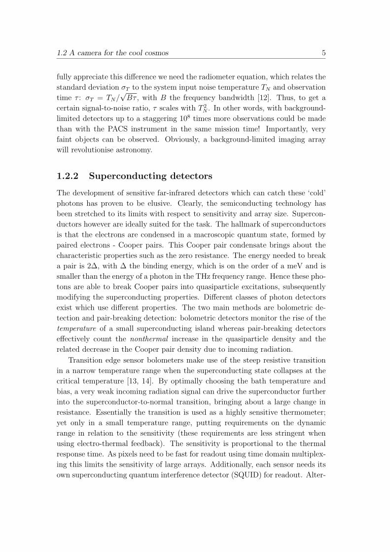
A promising new approach to the detection of photons is by using superconduct-
ing resonators [16]. The steady stream of incoming photons (with photon energy
larger than 2∆) breaks up Cooper pairs into unpaired excitations, changing their
respective densities, affecting the high frequency response of the superconductor.
-10 -5 0 5-30
-20
-10
0
Dw0/w
0tra
nsm
issio
n(d
B)
105(w-w
0)/w
0
ћw>2D
Cooper pairs
quasiparticles
D
E
N(E)
Figure 1.2: Left: A photon with energy ~ω is absorbed and breaks a Cooper pair,creating quasiparticle excitations on top of the thermal background. Middle: Thevariation in the Cooper pair and quasiparticle densities leads to a change in the kineticinductance. Right: Subsequently the resonance frequency of the circuit shifts.
1.2 A camera for the cool cosmos 7
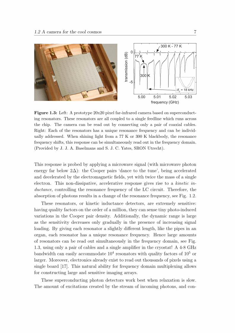
Figure 1.3: Left: A prototype 20x20 pixel far-infrared camera based on superconduct-ing resonators. These resonators are all coupled to a single feedline which runs acrossthe chip. The camera can be read out by connecting only a pair of coaxial cables.Right: Each of the resonators has a unique resonance frequency and can be individ-ually addressed. When shining light from a 77 K or 300 K blackbody, the resonancefrequency shifts, this response can be simultaneously read out in the frequency domain.(Provided by J. J. A. Baselmans and S. J. C. Yates, SRON Utrecht).
This response is probed by applying a microwave signal (with microwave photon
energy far below 2∆): the Cooper pairs ‘dance to the tune’, being accelerated
and decelerated by the electromagnetic fields, yet with twice the mass of a single
electron. This non-dissipative, accelerative response gives rise to a kinetic in-
ductance, controlling the resonance frequency of the LC circuit. Therefore, the
absorption of photons results in a change of the resonance frequency, see Fig. 1.2.
These resonators, or kinetic inductance detectors, are extremely sensitive:
having quality factors on the order of a million, they can sense tiny photo-induced
variations in the Cooper pair density. Additionally, the dynamic range is large
as the sensitivity decreases only gradually in the presence of increasing signal
loading. By giving each resonator a slightly different length, like the pipes in an
organ, each resonator has a unique resonance frequency. Hence large amounts
of resonators can be read out simultaneously in the frequency domain, see Fig.
1.3, using only a pair of cables and a single amplifier in the cryostat! A 4-8 GHz
bandwidth can easily accommodate 104 resonators with quality factors of 105 or
larger. Moreover, electronics already exist to read out thousands of pixels using a
single board [17]. This natural ability for frequency domain multiplexing allows
for constructing large and sensitive imaging arrays.
These superconducting photon detectors work best when relaxation is slow.
The amount of excitations created by the stream of incoming photons, and con-

8 Chapter 1. An eye for the sky
10-20 10-19 10-18 10-17 10-16 10-1510-6
10-5
10-4
10-3
10-2
10-1
Nb Ta Al
reco
mbi
natio
n tim
e (s
)
G-R noise equivalent power (W/Hz1/2)
Figure 1.4: The required quasiparticle recombination time versus generation-recombination limited noise equivalent power (NEP) for a typical resonator volumeand assuming unity efficiency, see Appendix A. Clearly, background-limited photom-etry (also see Fig. 1.1b) is possible with a recombination time around a millisecondand spectrophotometry is achievable with a recombination time in excess of tens ofmilliseconds.
sequently the detector sensitivity, is proportional to the relaxation time. The re-
laxation occurs by the pairing, or recombination, of these excitations into Cooper
pairs. The recombination process is a binary reaction; the recombination time is
reciprocally related to the density of quasiparticles available for recombination.
As the thermal quasiparticle density decreases exponentially with decreasing tem-
perature T as e−∆/kT , the recombination time and sensitivity increase with the
same temperature dependence as e∆/kT . The photon detection essentially relies on
counting Cooper pairs and quasiparticles, hence the noise is in principle given by
the the random thermal generation of quasiparticles and the subsequent recom-
bination: generation-recombination noise. The generation-recombination noise
limited NEP is: NEPG−R = 2∆√
Nqp/τr ∝ e−∆/kT , with Nqp the quasiparticle
number, τr the recombination time and assuming unity absorption efficiency; the
derivation is given in Appendix A. The recombination time needed to reach a
generation-recombination noise limited NEP is plotted in Fig. 1.4, illustrating
1.3 Matchmaking on a nanoscale 9
the importance of slow relaxation: background-limited detection (Fig. 1.1b) is
achievable with a recombination time around a millisecond or more.
1.3 Matchmaking on a nanoscale
Interestingly, the drive for sensitive detectors for observing the universe boils
down to understanding processes occurring at a microscopic scale; guided by
questions like: “How do electrons interact and exchange energy?”, and equally
important “What fluctuates at low temperatures, causing noise?”. These ques-
tions lie at the heart of solid state physics. At the same time, the temperatures
in the superconductor are so low that less than a billionth of the conduction
electrons are thermally excited and statistics of small numbers come into play.
The effect of microscopic fluctuations on macroscopic parameters can no longer
be considered small. Additionally, as these processes occur in superconducting
films with a thickness of only several tens of nanometers, these questions connect
to mesoscopic physics.
When photons are caught and their energy is dissipated, Cooper pairs are
broken and quasiparticles are excited; they are distributed over the energy in such
a way that they can no longer be described by a temperature: the distribution
has become nonthermal and the superconductor is in a nonequilibrium state.
The superconducting resonator becomes a sensitive probe to the microscopic
processes of scattering and recombination, occurring at the crossroads of the
energy exchange via inelastic electron-electron and electron-lattice interaction.
Additionally, it is a useful tool to elucidate the physical mechanisms behind for
example the influence of disorder and the possible interaction with magnetic
atoms. Importantly, if the perturbation is small, the relaxation process reveals a
great deal about the equilibrium properties.
In principle these properties are controlled by the superconductor, but pos-
sibly present dipoles and magnetic spins can couple to the electric and mag-
netic fields in the resonator; additionally they can influence the electron system.
Indeed, configurational defects with a dipole moment, that fluctuate between
low-lying energy states, have already been found in superconducting resonators
through the temperature dependence of the resonance frequency [18]. These
dipole systems have also been conjectured to cause noise by random fluctuation.
Interestingly, superconducting resonators made of a variety of superconducting
materials and dielectric substrates show significant frequency noise. The noise
has been observed to increase with decreasing temperature [19, 20], contrary to
for example noise arising from thermal fluctuations, forming a major issue for
10 Chapter 1. An eye for the sky
low temperature applications.
The energy exchange and noise at low temperatures are not only of funda-
mental importance but are of practical value in a broad context: many devices
critically depend on the low temperature properties of superconducting films. A
prime example is the research into quantum information processing using super-
conducting systems. A normal bit is either a logical 0 or 1, but a quantum bit is
represented by the superposition of the two. The quantum bit can be stored in
the charge on a very small superconducting island, the flux in a superconducting
ring, or the phase difference between superconductors over a tunnel barrier [21].
Yet, in all these systems the evolution in time of the qubit state seems strongly
disturbed by the influence of the environment. Superconducting islands seem to
have more quasiparticle excitations than theoretically predicted [22, 23], an issue
called ‘quasiparticle poisoning’, dipole fluctuators have been encountered in thin
oxide barriers [24], and recent measurements suggest the presence of unpaired
spins on the surfaces of superconductors [25]. The decoherence has proved to be
a tremendous obstacle for quantum computation.
The desire for sensitive far-infrared imaging arrays stimulates the research into
fundamental physical processes: the relaxation and noise at these low tempera-
tures in superconductors are virtually untrodden territory. This forms the main
theme of this thesis. As such, the recombination, the matchmaking of quasipar-
ticles into Cooper pairs, as well as the happy marriage between astronomy and
mesoscopic physics, can truly be considered as matchmaking on a nanoscale.
1.4 This thesis
This thesis describes a series of experiments using superconducting resonators de-
signed to elucidate the physical mechanisms behind quasiparticle relaxation and
noise, as well as to identify the fundamental limitations to using these resonators
as photon detectors.
Chapter 2 : In this chapter we introduce the most relevant concepts of super-
conductivity, relaxation and noise, forming a basis for the topics of this thesis.
Chapter 3 : Here we focus on the important aspects of planar superconducting
resonators, which are used throughout this thesis: we describe the geometry and
fabrication, present the microwave properties for characterising these resonators
and provide a practical guide for probing their properties.
Chapter 4 : Here we find that the quality factors of the superconducting res-
onators increase with decreasing temperature, yet saturate at low temperatures,
exhibiting a significant dependence on the power levels inside the resonator.
1.4 This thesis 11
Moreover, we find a clear nonmonotonic temperature dependence in the reso-
nance frequency of Nb and Ta resonators, signalling the presence of dipole tun-
nelling systems. Additionally, preliminary measurements indicate the presence
of significant noise in the resonance frequency.
Chapter 5 : We directly probe the low temperature recombination process
for the first time and find recombination times as long as a millisecond for Al
and several tens of microseconds for Ta using high quality factor superconduct-
ing resonators. Additionally, we find a remarkable saturation of the relaxation
time, indicating the presence of a second recombination process dominant at low
temperatures in the superconducting films. Measurements of the noise spectral
density under continuous illumination confirm the relaxation process is dominated
by a single timescale.
Chapter 6 : Triggered by the low temperature saturation of the relaxation
time and its reminiscence to experimental results with normal metals, we extend
on the research in Chapter 5 and investigate the influence of magnetic impurities.
We find that the low temperature recombination process is strongly enhanced by
the implantation of magnetic as well as nonmagnetic atoms, pointing towards
disorder, possibly at the superconductor surface.
Chapter 7 : In this chapter we show that NbTiN on hydrogen passivated
Si does not exhibit the peculiar nonmonotonic temperature dependence of the
resonance frequency previously found in the other materials used. Moreover, we
demonstrate that we can re-establish this nonmonotonic temperature dependence
by covering the superconductor with a SiO2 dielectric layer, scaling with the
thickness. In contrast, the noise increases when covering the superconductor,
but does not increase with further thickness, indicating the noise predominantly
arises at the superconductor-dielectric interface and/or the interface between the
dielectric layer and the substrate.
Chapter 8 : We find that the noise can be significantly decreased by widening
the geometry of the resonator waveguide. Additionally, the noise is lowest when
using hydrogen passivated Si instead of sapphire as substrate, suggesting that
the superconductor-substrate interface plays an important role as well.
Apart from the elucidating research into fundamental processes in condensed
matter physics and into limitations to using superconducting resonators as pho-
ton detectors, this thesis is also a record of the joint pioneering work of the
Delft University of Technology and the SRON Netherlands Institute for Space
Research, which resulted in an increase of the sensitivity with three orders of
magnitude during the course of this thesis. Noise equivalent powers as low as
6 ·10−19 W/√
Hz (measured electrically) have been reached [26], which is already

12 Chapter 1. An eye for the sky
low enough for photometry and requires only one last order of magnitude for
imaging spectrometry, limited by the universe itself, to come into focus (see Fig.
1.1b). Already large efforts are being put into the development of far-infrared
imaging instruments based on these superconducting resonators; for ground based
imaging such as the Caltech Submillimeter Observatory (CSO) [27], the IRAM
30m telescope, the Atacama Pathfinder Experiment (APEX) as well as for space-
based telescopes such as the Spica far-infrared instrument (SAFARI) on the fu-
ture Space Infrared telescope for Cosmology and Astrophysics (SPICA) satellite.
These imaging arrays will be a valuable contribution to astronomy; sensing the
universe alongside heterodyne receivers, such as the superconducting mixers from
our group which are employed in the Heterodyne Instrument for the Far-Infrared
(HIFI) of the Herschel Space Observatory [28], and the Atacama Large Millimeter
Array (ALMA) [29]. As for the future discoveries in astronomy using supercon-
ducting resonators: that remains, in every meaning of the words, written in the
stars.
References
[1] D. Leisawitz et al., Scientific motivation and technology requirements for theSPIRIT and SPECS far-infrared/submillimeter space interferometers, Proc. SPIE4013, 36 (2000).
[2] P. G. Ferreira, The cosmic microwave background, Physics World 16, 27 (2003).
[3] G. Hinshaw, WMAP data put cosmic inflation to the test, Physics World 19, 16(2006).
[4] A. Noriega-Crespo et al., A new look at stellar outflows: Spitzer observations ofthe HH 46/47 system, Astrophys. J. Sup. Series 154, 352 (2004).
[5] Detector needs for long wavelength astrophysics, a report by the Infrared, Submil-limeter, and Millimeter Detector Working Group, NASA, June 2002.
[6] Community plan for far-infrared/submillimeter space astronomy, Februari 2003.
[7] T. G. Phillips and J. Keene, Submillimeter astronomy, Proc. IEEE. 80, 1662(1992).
[8] D. J. Benford, S. Harvey Moseley, Cryogenic detectors for infrared astronomy:the Single Aperture Far-InfraRed (SAFIR) Observatory, Nucl. Instr. Meth. Res.A 520, 379 (2004).
[9] P. L. Richards and C. R. McCreight, Infrared detectors for astrophysics, PhysicsToday 58, 41 (2005).
[10] PACS Observer’s Manual, May 2007.

References 13
[11] W. Holland et al., SCUBA-2: a 10,000 pixel submillimeter camera for the JamesClerk Maxwell Telescope, Proc. SPIE 6275, 62751E (2006).
[12] R. H. Dicke, The measurement of thermal radiation at microwave frequencies,Rev. Sci. Instr. 17, 268 (1946).
[13] K. D. Irwin and G. C. Hilton, Transition-Edge Sensors in Cryogenic ParticleDetection, edited by C. Enss (Springer-Verlag, Berlin-Heidelberg, 2005)
[14] D. J. Benford and S. Harvey Moseley, Astronomy Applications of SuperconductingTransition Edge Sensor Bolometer Arrays, Proc. Space Detectors Workshop, 2000.
[15] A. Peacock, P. Verhoeve, N. Rando, A. van Dordrecht, B. G. Taylor, C. Erd, M. A.C. Perryman, R. Venn, J. Howlett, D. J. Goldie, J. Lumley, and M. Wallis, Singleoptical photon detection with a superconducting tunnel junction, Nature 381, 135(1996).
[16] P. K. Day, H. G. LeDuc, B. A. Mazin, A. Vayonakis, and J. Zmuidzinas, A broad-band superconducting detector suitable for use in large arrays, Nature 425, 817(2003).
[17] S. J. C. Yates, A. M. Baryshev, J. J. A. Baselmans, B. Klein, R. Gusten, FFTSreadout for large arrays of Microwave Kinetic Inductance Detectors, arXiv:0903.2431.
[18] J. Gao, M. Daal, A. Vayonakis, S. Kumar, J. Zmuidzinas, B. Sadoulet, B. A.Mazin, P. K. Day, and H. G. LeDuc, Experimental evidence for a surface distri-bution of two-level systems in superconducting lithographed microwave resonators,Appl. Phys. Lett. 92, 152505 (2008).
[19] R. Barends, H. L. Hortensius, T. Zijlstra, J. J. A. Baselmans, S. J. C. Yates, J.R. Gao, and T. M. Klapwijk, Contribution of dielectrics to frequency and noise ofNbTiN superconducting resonators, Appl. Phys. Lett. 92, 223502 (2008).
[20] S. Kumar, J. Gao, J. Zmuidzinas, B. A. Mazin, H. G. LeDuc, and P. K. Day,Temperature dependence of the frequency and noise of superconducting coplanarwaveguide resonators, Appl. Phys. Lett. 92, 123503 (2008).
[21] M. H. Devoret, A. Wallraff, and J. M. Martinis, Superconducting Qubits: A ShortReview, arXiv:cond-mat/0411174.
[22] J. Aumentado, M. W. Keller, J. M. Martinis, and M. H. Devoret, NonequilibriumQuasiparticles and 2e Periodicity in Single-Cooper-Pair Transistors, Phys. Rev.Lett. 92, 066802 (2004).
[23] J. M. Martinis, M. Ansmann and J. Aumentado, Energy Decay in JosephsonQubits from Non-equilibrium Quasiparticles, arXiv:0904.2171.
[24] J. M. Martinis, K. B. Cooper, R. McDermott, M. Steffen, M. Ansmann, K. D.Osborn, K. Cicak, S. Oh, D. P. Pappas, R. W. Simmonds, and C. C. Yu, Deco-herence in Josephson Qubits from Dielectric Loss, Phys. Rev. Lett. 95, 210503(2005).
14 Chapter 1. An eye for the sky
[25] S. Sendelbach, D. Hover, A. Kittel, M. Muck, J. M. Martinis, and R. McDermott,Magnetism in SQUIDs at millikelvin temperatures, Phys. Rev. Lett. 100, 227006(2008).
[26] J. J. A. Baselmans, S. J. C. Yates, R. Barends, Y. J. Y. Lankwarden, J. R. Gao,H. F. C. Hoevers, and T. M. Klapwijk, Noise and sensitivity of aluminum kineticinductance detectors for sub-mm astronomy, J. Low Temp. Phys. 151, 524 (2008);and unpublished results.
[27] J. Schlaerth, A. Vayonakis, P. Day, J. Glenn, J. Gao, S. Golwala, S. Kumar,H. LeDuc, B. Mazin, J. Vaillancourt, and J. Zmuidzinas, A Millimeter and Sub-millimeter Kinetic Inductance Detector Camera, J. Low Temp. Phys. 151, 684(2008).
[28] B. D. Jackson, G. de Lange, T. Zijlstra, M. Kroug, J. W. Kooi, J. A. Stern, and T.M. Klapwijk, Low-Noise 0.8-0.96 and 0.96-1.12 THz Superconductor-Insulator-Superconductor Mixers for the Herschel Space Observatory, IEEE Trans. Micr.Theory and Tech. 54, 547 (2006).
[29] C. Kasemann, R. Gusten, S. Heyminck, B. Klein, T. Klein, S. D. Philipp, A.Korn, G. Schneider, A. Henseler, A. Baryshev, and T. M. Klapwijk, CHAMP+: apowerful array receiver for APEX, Proc. SPIE 6275, 62750N (2006).
Chapter 2
Relaxation, low frequency fluctuation
and the response to
high frequency radiation
15
16 Chapter 2. Relaxation, fluctuation and the response to radiation
2.1 Cooper pairs and quasiparticle excitations
In metallic solids, many of their properties are controlled by only the few electrons
in the outermost shells of the ions. These electrons are so weakly bound that
they become delocalised and act as mobile charge carriers, bringing about the
characteristic conductivity of metals. At a first glance, metals are adequately
described by treating these conduction electrons as a gas of fermions consisting
of free, noninteracting electrons, constrained only by the Pauli exclusion principle;
the Sommerfeld theory of metals [1].
In many metals the electron density is huge, being on the order of 1023 1/cm3,
and the mutual interaction needs to be considered. In a real gas, with increas-
ing density and decreasing kinetic energy (by decreasing the temperature) the
interactions become so dominant that the gas changes into a liquid. Analogously,
with strong interactions the picture of charge carriers in metallic solids as a free
electron Fermi gas needs to be reanalysed. Electrons interact by pushing each
other away due to their charge, i.e. Coulomb repulsion. At the same time this
repulsion is reduced by the screening of the electron charge by other electrons
to relatively short distances on the order of the interatomic spacing; effectively,
an electron is surrounded by its nearby screening cloud. When a particle is in
motion, it moves together with the surrounding distortion brought about by the
screened Coulomb interaction, perturbing the other electrons in the vicinity. As
such, these charge carriers can no longer be treated purely as a collection of single
electrons in a Fermi gas, but have to be thought of as electron-like particles in a
Fermi liquid, so-called quasiparticles [2].
The consequences are far-reaching. As a quasiparticle is in essence a many-
body process, quasiparticles are interdependent. Additionally, quasiparticle states
are no longer stationary and have a finite lifetime. The quasiparticles adopt the
role of charge carriers, affecting the electronic properties of the metal, from con-
ductivity to the dielectric response. In normal metals these are referred to as
Landau quasiparticles. Most of the changes are subtle, and the Sommerfeld free
electron model is still a good starting point for many applications when using an
effective density of states or particle mass, and we can loosely refer to Landau
quasiparticles as ‘electrons’. Foremost, the interdependence of quasiparticles con-
stitutes a fundamental shift in the approach to elastic and inelastic interactions:
the non-equilibrium processes and fluctuations in metallic systems.
In metallic solids with a strong electron-lattice coupling, in addition to the
Coulomb repulsion an attractive interaction can exist: in their motion, conduc-
tion electrons distort the lattice by attracting the positively charged ions. Due to
the delayed response of the lattice a positively charged region is left in the wake
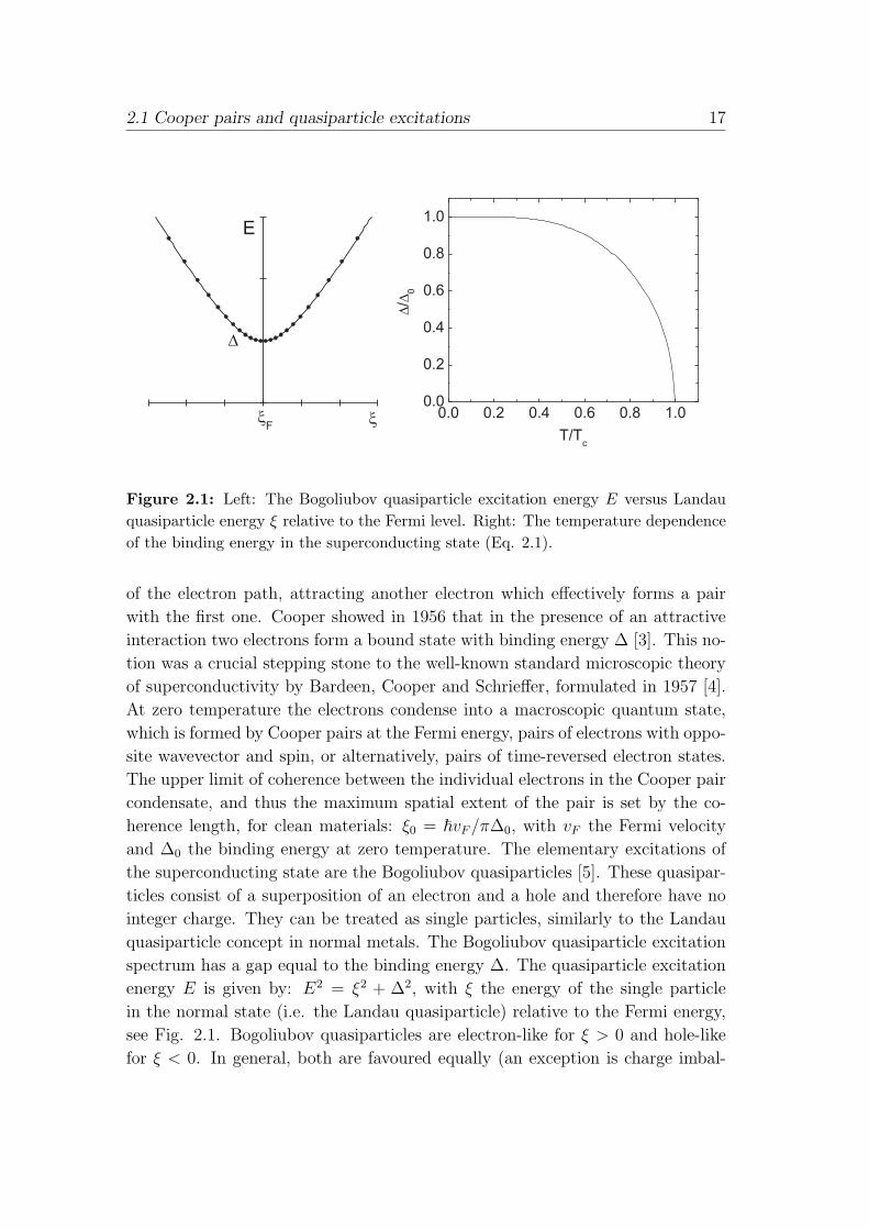
2.1 Cooper pairs and quasiparticle excitations 17
x
D
xF
E
0.0 0.2 0.4 0.6 0.8 1.00.0
0.2
0.4
0.6
0.8
1.0
D/D
0
T/Tc
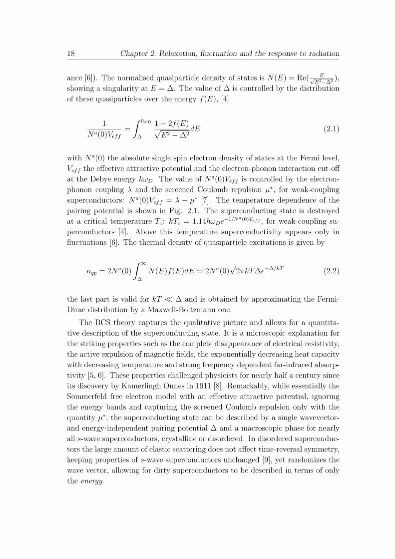
Figure 2.1: Left: The Bogoliubov quasiparticle excitation energy E versus Landauquasiparticle energy ξ relative to the Fermi level. Right: The temperature dependenceof the binding energy in the superconducting state (Eq. 2.1).
of the electron path, attracting another electron which effectively forms a pair
with the first one. Cooper showed in 1956 that in the presence of an attractive
interaction two electrons form a bound state with binding energy ∆ [3]. This no-
tion was a crucial stepping stone to the well-known standard microscopic theory
of superconductivity by Bardeen, Cooper and Schrieffer, formulated in 1957 [4].
At zero temperature the electrons condense into a macroscopic quantum state,
which is formed by Cooper pairs at the Fermi energy, pairs of electrons with oppo-
site wavevector and spin, or alternatively, pairs of time-reversed electron states.
The upper limit of coherence between the individual electrons in the Cooper pair
condensate, and thus the maximum spatial extent of the pair is set by the co-
herence length, for clean materials: ξ0 = ~vF /π∆0, with vF the Fermi velocity
and ∆0 the binding energy at zero temperature. The elementary excitations of
the superconducting state are the Bogoliubov quasiparticles [5]. These quasipar-
ticles consist of a superposition of an electron and a hole and therefore have no
integer charge. They can be treated as single particles, similarly to the Landau
quasiparticle concept in normal metals. The Bogoliubov quasiparticle excitation
spectrum has a gap equal to the binding energy ∆. The quasiparticle excitation
energy E is given by: E2 = ξ2 + ∆2, with ξ the energy of the single particle
in the normal state (i.e. the Landau quasiparticle) relative to the Fermi energy,
see Fig. 2.1. Bogoliubov quasiparticles are electron-like for ξ > 0 and hole-like
for ξ < 0. In general, both are favoured equally (an exception is charge imbal-
18 Chapter 2. Relaxation, fluctuation and the response to radiation
ance [6]). The normalised quasiparticle density of states is N(E) = Re( E√E2−∆2 ),
showing a singularity at E = ∆. The value of ∆ is controlled by the distribution
of these quasiparticles over the energy f(E), [4]
1
Na(0)Veff
=
∫ ~ωD
∆
1− 2f(E)√E2 −∆2
dE (2.1)
with Na(0) the absolute single spin electron density of states at the Fermi level,
Veff the effective attractive potential and the electron-phonon interaction cut-off
at the Debye energy ~ωD. The value of Na(0)Veff is controlled by the electron-
phonon coupling λ and the screened Coulomb repulsion µ∗, for weak-coupling
superconductors: Na(0)Veff = λ − µ∗ [7]. The temperature dependence of the
pairing potential is shown in Fig. 2.1. The superconducting state is destroyed
at a critical temperature Tc: kTc = 1.14~ωDe−1/Na(0)Veff , for weak-coupling su-
perconductors [4]. Above this temperature superconductivity appears only in
fluctuations [6]. The thermal density of quasiparticle excitations is given by
nqp = 2Na(0)
∫ ∞
∆
N(E)f(E)dE ' 2Na(0)√
2πkT∆e−∆/kT (2.2)
the last part is valid for kT ¿ ∆ and is obtained by approximating the Fermi-
Dirac distribution by a Maxwell-Boltzmann one.
The BCS theory captures the qualitative picture and allows for a quantita-
tive description of the superconducting state. It is a microscopic explanation for
the striking properties such as the complete disappearance of electrical resistivity,
the active expulsion of magnetic fields, the exponentially decreasing heat capacity
with decreasing temperature and strong frequency dependent far-infrared absorp-
tivity [5, 6]. These properties challenged physicists for nearly half a century since
its discovery by Kamerlingh Onnes in 1911 [8]. Remarkably, while essentially the
Sommerfeld free electron model with an effective attractive potential, ignoring
the energy bands and capturing the screened Coulomb repulsion only with the
quantity µ∗, the superconducting state can be described by a single wavevector-
and energy-independent pairing potential ∆ and a macroscopic phase for nearly
all s-wave superconductors, crystalline or disordered. In disordered superconduc-
tors the large amount of elastic scattering does not affect time-reversal symmetry,
keeping properties of s-wave superconductors unchanged [9], yet randomizes the
wave vector, allowing for dirty superconductors to be described in terms of only
the energy.
2.2 Inelastic interaction at millikelvin temperatures 19
2.2 Inelastic interaction at millikelvin tempera-
tures
In thermal equilibrium the distribution of the quasiparticles over the energy is
given by the Fermi-Dirac distribution function at an electron temperature T ,
fFD(E) =1
1 + eE/kT(2.3)
with E the energy relative to the Fermi level. When the electronic system is
perturbed, by the absorption of energy or injection of quasiparticles, the system
is driven out of the equilibrium state. The system can be described by an elevated
electron temperature when instantaneous energy exchange is assumed between
the quasiparticles, such as in the hot filament of a light bulb. However, at low
temperatures the strength of the interactions weaken, most clearly due to the
decrease of k space available for scattering near the Fermi level; additionally the
phonon density decreases, in turn decreasing the energy exchange between the
electron system and the lattice. Then, the quasiparticle energy distribution is no
longer thermal and a nonequilibrium state results, controlled by the competition
between the driving force and the inelastic interactions.
We start by discussing the energy exchange at low temperatures in normal
metals and focus on the recent experiments. These experiments not only neatly
clarify the shape and degree of nonequilibrium which can occur in for example
metallic wires, but also illustrate that inelastic scattering at mK temperatures
is unexplored territory, elucidating very recently the important role of dilute
concentrations of magnetic impurities. These experiments provide a framework
for investigating the equilibration processes in superconductors. Subsequently,
we review the inelastic interaction processes that take place in superconducting
films; here, the electron-phonon processes play an important role in quasiparticle
scattering and quasiparticle recombination, the latter plays a dominant role in
the low temperature equilibration. Finally, we discuss the influence of magnetic
impurities on the superconducting state.
2.2.1 Scattering in the normal state
Inelastic scattering in normal metals has been investigated by nonequilibrium
experiments as well as experiments on quasiparticle dephasing, probed via weak
localisation. As elastic scattering does not randomise the quasiparticle phase,
dephasing is a measure for the inelastic scattering time. It has become clear that
at high temperature the inelastic scattering is mainly due to electron-phonon
20 Chapter 2. Relaxation, fluctuation and the response to radiation
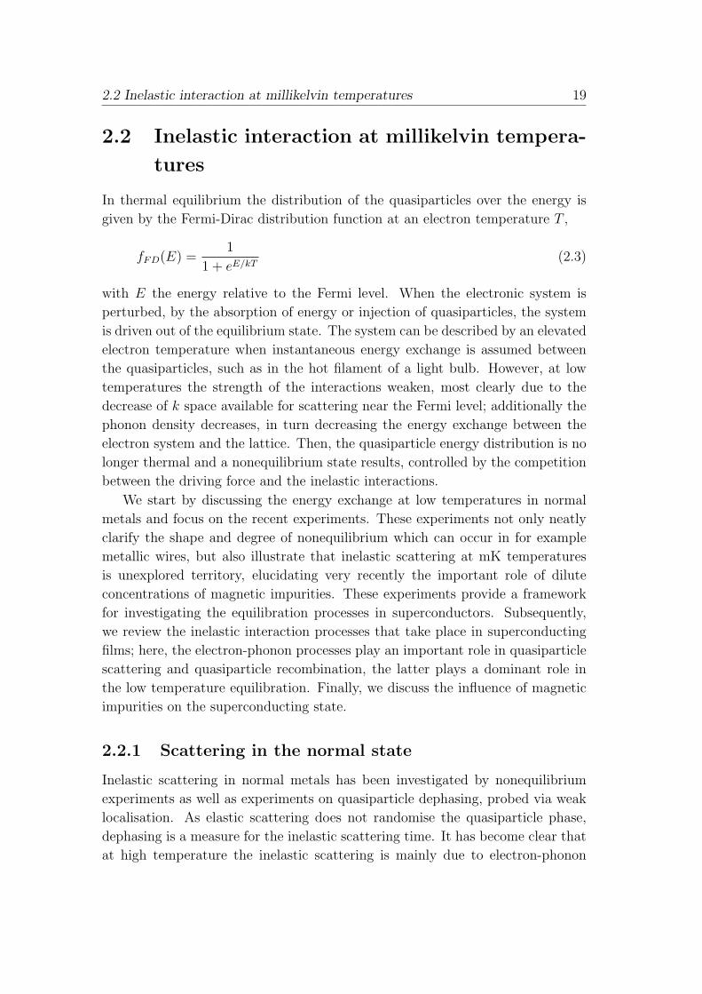
Figure 2.2: Left: A mesoscopic wire placed in between electrodes, two probing fingersare attached to the wire. Right: The distribution function inside the wire resemblesa two-step function for weak inelastic scattering and is thermal in the limit of strongscattering. The distribution function becomes more thermal-like for increasing wirelengths, illustrating the competition between diffusion and inelastic scattering.
interaction whereas at low temperatures electron-electron scattering dominates,
for a review see Ref. [10]. Both the temperature dependence as well as the
prefactor of the scattering rate is controlled by the disorder and dimensionality
of the film, the crossover between these two regimes lies roughly on the order
of 1 K, for example for Al [11]. Only in specifically designed systems electron-
photon processes play a significant role [12]. In practice, the emphasis for low
temperature scattering lies on the interactions among quasiparticles.
In 1997 Pothier et al. [13] devised a way to probe the inelastic interactions
by creating a nonequilibrium distribution in a voltage-biased mesoscopic wire,
see Fig. 2.2. The local distribution is probed with normal metal-insulator-
superconductor junctions on top of the wire. In the absence of inelastic interac-
tions, the distribution in the wire is given by a two-step distribution function,
resulting from the Boltzmann transport equation
f(x,E) = (1− x)fFD(E + eV/2) + xfFD(E − eV/2) (2.4)
with x the coordinate along the wire and fFD the Fermi-Dirac distribution func-
tion at the bath temperature. With strong inelastic scattering this distribution
is rounded to a thermal one with a local, elevated temperature. Moreover, at
higher voltages quasiparticles with higher energies start to play a role, allow-
ing for probing interaction at higher energies. The actual distribution function
is therefore a result of the competition between diffusion and energy-dependent
inelastic scattering.

2.2 Inelastic interaction at millikelvin temperatures 21
0.1 1
1
10
TK
t(
)n
s
T K( )
f
Ag, 6N (99.9999%)
Ag, 5N+0.3 ppm Mn
Ag, 5N
Ag, 5N+1 ppm Mn
-0.1 0.0 0.1 0.2
0.8
0.9
1.0
1.1
1.2
Rtd
I/d
V-0.1 0.0 0.1 0.2
0.9
1.0
implanted
U=0.1 mV
bare
V (mV)V (mV)
Figure 2.3: Left: The differential conductance, measured in a similar device as shownin Fig. 2.2, shows a single dip for a thermal distribution and two distinct dips for atwo-step distribution. The presence of magnetic impurities leads to a stronger thermalrounding, i.e. stronger inelastic scattering. The recovery of a single dip for increasingmagnetic field (from bottom to top: B=0.3 to 2.1 T with steps of 0.3 T) is an addi-tional indication for the influence of magnetic impurities. Right: The low temperaturequasiparticle dephasing time in high purity Ag is strongly reduced by the presence ofonly a dilute concentration of magnetic impurities.
The experiment was performed at temperatures of 25 mK in Cu wires. Whereas
a two-step distribution was established in the wire for small bias voltages, for in-
creasing voltages the distribution function was found to be more smeared, see
Fig. 2.2. From these results the strength as well as the energy dependence of
the inelastic electron-electron scattering was extracted; represented by the in-
teraction kernel K(ε), with ε the exchanged energy (see Ref. [13] for details).
This kernel was expected to follow K(ε) ∝ 1/ε3/2, reflecting screened Coulomb
interaction in a quasi one-dimensional wire [14, 15]. Yet, the experimental re-
sults indicated K(ε) ∝ 1/ε2±0.1. Additionally, the strength of the interaction was
stronger than predicted. These results signalled the presence of another inelastic
scattering process dominating at these low temperatures.
In later experiments [16] a magnetic field dependence of the interaction in
mesoscopic wires was found as well as a similar energy dependence previously
obtained by Pothier et al., suggesting the influence of magnetic impurities. The
Kondo effect (see Chapter 2.2.3) is diminished as spin-flip scattering becomes an
inelastic process due to the Zeeman splitting. At the same time, low temperature
quasiparticle phase coherence times were significantly decreased by implanting
magnetic impurities [17, 18], see Fig. 2.3. Recently, Huard et al. [19] have
shown that the inelastic scattering among quasiparticles is strongly strengthened
by implanting dilute concentrations (as low as 1 ppm) of magnetic impurities
22 Chapter 2. Relaxation, fluctuation and the response to radiation
in similar mesoscopic Ag wires, in agreement with two-particle collisions in the
presence of Kondo impurities [20] (Fig. 2.3). Further experiments show that
the implantation procedure does not introduce extra dephasing in Ag [21]. This
set of experiments shows that at low temperatures timescales for quasiparticles
are limited by dilute concentrations of magnetic impurities, most notably the
inelastic scattering between quasiparticles.
2.2.2 Quasiparticle recombination in superconducting films
A binary reaction
In superconductors, inelastic interaction becomes apparent when driving the su-
perconductor into a nonequilibrium state. Experimentally, the nonequilibrium
state can be established by injecting electrons or by creating quasiparticle exci-
tations by inserting energy in the electron system through, for example, optical
excitation. The absorption of optical photons excites quasiparticles to high ener-
gies, in turn starting a fast quasiparticle downconversion cascade. This cascade
results in a large number of quasiparticles just above the superconducting gap
within timescales ranging between 100 ps to 10 ns [22, 23]. Subsequent equi-
libration of the superconducting state takes place by the redistribution of the
quasiparticles over the energy, which is accomplished by the energy exchange
among quasiparticles and between quasiparticles and the lattice, as well as by
recombination. Recombination is a binary process, quasiparticles with opposite
wavevector and spin combine to form Cooper pairs, the energy is transferred to
another excitation. It is the most important process as it allows both for large
energy exchanges as well as for the recovery of the quasiparticle and Cooper pair
density to their equilibrium values. It also is the slowest and therefore limiting
process for equilibration. We therefore limit the discussion to recombination.
Historically, recombination has been investigated at temperatures close to the
critical temperature (see for example the first experiments by Miller et al. [24]).
Here it was found that electron-phonon processes dominate for two reasons: One,
recombination with phonon emission is orders of magnitude faster than recombi-
nation with photon emission [25]. Two, recombination with phonon emission is
a binary reaction, following τr ∝ e∆/kT due to the availability of quasiparticles
[26]. This while recombination with electron-electron interaction only is a tre-
nary reaction (two quasiparticles recombine and transfer their energy to a third),
following τr ∝ e2∆/kT [27]. Obviously with decreasing temperature a binary re-
action is much more probable than a trenary reaction. Moreover the energy gap
develops, allowing large energy exchanges only through electron-phonon scatter-
2.2 Inelastic interaction at millikelvin temperatures 23
0.05 0.1 0.2 0.3 0.4 0.510-10
10-8
10-6
10-4
10-2
100
1015
1017
1019
1021
1023
1025
n qp (1
/m3 )
r() (
s)
T/Tc
Nb Ta Al
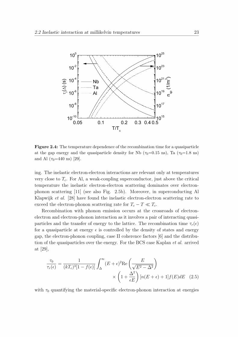
Figure 2.4: The temperature dependence of the recombination time for a quasiparticleat the gap energy and the quasiparticle density for Nb (τ0=0.15 ns), Ta (τ0=1.8 ns)and Al (τ0=440 ns) [29].
ing. The inelastic electron-electron interactions are relevant only at temperatures
very close to Tc. For Al, a weak-coupling superconductor, just above the critical
temperature the inelastic electron-electron scattering dominates over electron-
phonon scattering [11] (see also Fig. 2.5b). Moreover, in superconducting Al
Klapwijk et al. [28] have found the inelastic electron-electron scattering rate to
exceed the electron-phonon scattering rate for Tc − T ¿ Tc.
Recombination with phonon emission occurs at the crossroads of electron-
electron and electron-phonon interaction as it involves a pair of interacting quasi-
particles and the transfer of energy to the lattice. The recombination time τr(ε)
for a quasiparticle at energy ε is controlled by the density of states and energy
gap, the electron-phonon coupling, case II coherence factors [6] and the distribu-
tion of the quasiparticles over the energy. For the BCS case Kaplan et al. arrived
at [29],
τ0
τr(ε)=
1
(kTc)3[1− f(ε)]
∫ ∞
∆
(E + ε)2Re
(E√
E2 −∆2
)
×(
1 +∆2
εE
)[n(E + ε) + 1]f(E)dE (2.5)
with τ0 quantifying the material-specific electron-phonon interaction at energies
24 Chapter 2. Relaxation, fluctuation and the response to radiation
near the gap and n(E) the phonon distribution function. The value of τ0 is related
to the electron-phonon spectral function α2F (E), in the above expression we
follow the assumption by Kaplan et al. [29] that the electron-phonon interaction
α2 is only weakly dependent on the low energies concerned. Additionally, for a
three dimensional system for the Debye phonon density of states: F (E) ∝ E2,
hence for the electron-phonon spectral function: α2F (E) ∝ E2.
Assuming a thermal distribution of quasiparticles and phonons, for low tem-
peratures the recombination time can be approximated by
τ0
τr(∆)=√
π
(2∆
kTc
)5/2 √T
Tc
e−∆/kT =(2∆)2
(kTc)3
nqp
2Na(0)(2.6)
using Eq. 2.2, with Na(0) the absolute single spin density of states at the Fermi
level. Eq. 2.6 shows the process in its most simple form: the recombination
time is controlled by the quasiparticle density and the electron-phonon interac-
tion. The recombination time is shown for various materials in Fig. 2.4. It
increases exponentially with decreasing temperature, reciprocal to the thermal
quasiparticle density. The temperature dependence is due to the Fermi-Dirac
distribution, the prefactor is set by the value of the electron-phonon coupling τ0.
The possible reabsorption by the condensate of 2∆-phonons, emitted during
recombination, leads to an increase of the relaxation time. This phonon trapping
is controlled by the phonon escape time τesc [37], which depends on the acoustical
film-substrate matching, and the phonon pair breaking time τpb [29]. For τesc ¿τpb the phonons quickly leave the superconducting film and their distribution is
close to equilibrium. For τesc À τpb energy is being put back in the electron
system by reabsorption. Consequently, the relaxation time increases, given by:
τ = τr(1 + τesc/τpb), for τr À τesc, τpb, which is the case at the low temperatures
we use [38]. The values of τesc and τpb are hardly temperature dependent [29],
hence the exponential increase of the relaxation time with decreasing temperature
remains unchanged, but the prefactor is affected. To quantify, using τesc = 4d/ηu,
with d the film thickness, η the acoustic film-substrate transparency and u the
phonon velocity [39] and using values for τpb from Ref. [29], for Al: (1+τesc/τpb) ∼1 and for Ta: (1 + τesc/τpb) ∼ 10.
The role of disorder
The inelastic electron-phonon processes are sensitive to disorder. This disorder
dependence has been investigated in normal metals using hot electron exper-
iments and by measurements of the phase coherence time. The temperature
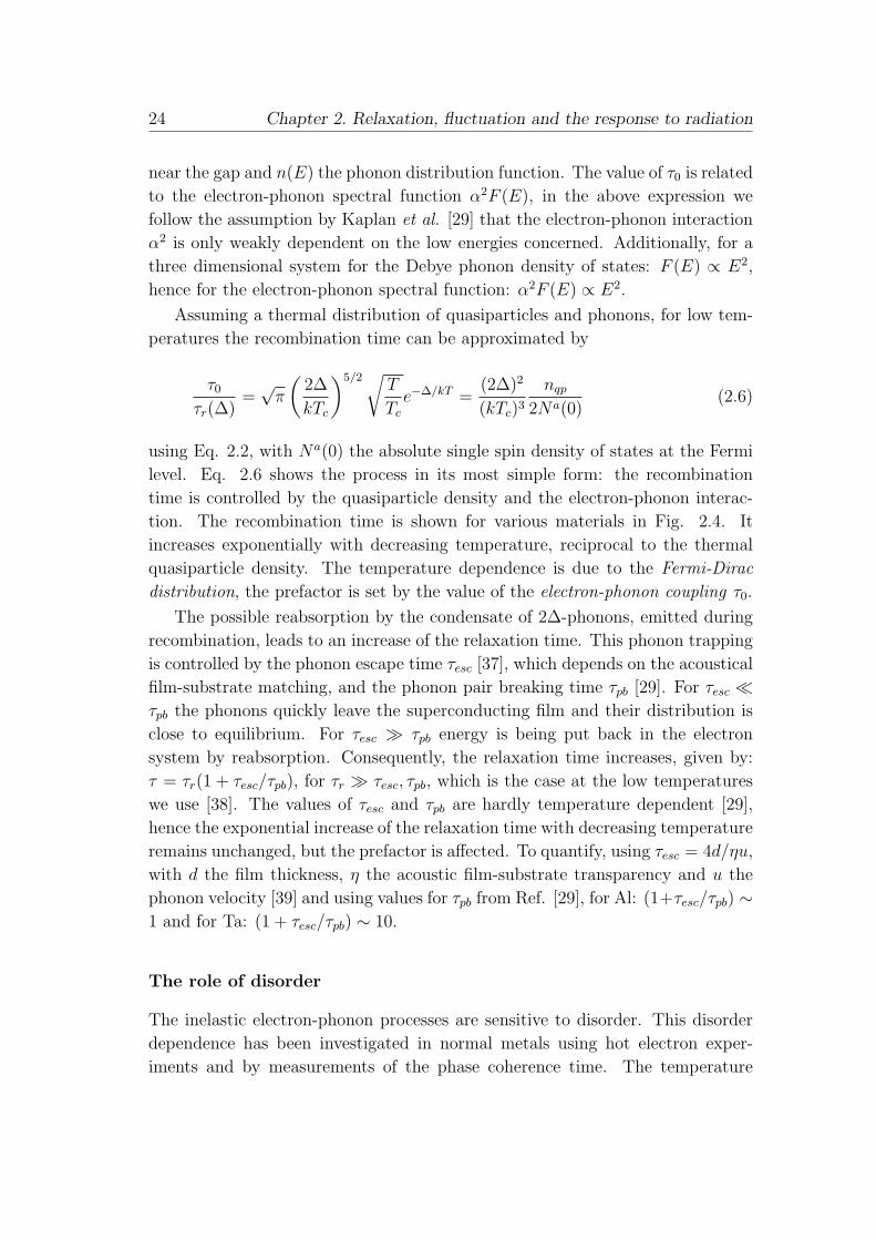
2.2 Inelastic interaction at millikelvin temperatures 25
Nb Al
(a) (b)
T-2
T-3
(c)
0.1 110
-7
10-6
10-5
10-4
10-3
10-2
10-1
t()
s
T (K)
Hf
Ti
T-4
Figure 2.5: Three different temperature dependences of the inelastic electron-phononscattering time in superconducting films just above the critical temperature. (a) Aquadratic temperature dependence (τep ∝ 1/T 2) has been found for Nb films usinghot electron experiments [34]. The inset shows the dependence on the electron meanfree path through the diffusion constant. (b) The phase coherence time for Al filmsshows at high temperatures a cubic temperature dependence, τ ∝ 1/T 3, consistent withinelastic electron-phonon scattering. At low temperatures electron-electron scatteringdominates (following τ ∝ 1/T ) [11]. (c) For Hf and Ti τep ∝ 1/T 4 has been found usinghot electron experiments [35].
dependent inelastic electron-phonon scattering time is given by [30]
1
τep
=4π
~
∫ ∞
0
α2F (E)
sinh(E/kT )dE (2.7)
Obviously, if α2F (E) ∝ En, then τep ∝ 1/T n+1. In clean three-dimensional
systems where the electron mean free path is long, scattering is mainly by longi-
tudinal phonons, leading to a cubic temperature dependence, τep ∝ 1/T 3 [31]. In
an acoustically dirty film where quasiparticles experience numerous elastic scat-
tering events within the wavelength of a phonon the interaction can be drastically
changed [32, 33]. Depending on the nature of the impurity, whether they ‘fol-
low the lattice motion’ or are ‘pinned’, the scattering can be both weakened as
well as enhanced, respectively. In normal metals this leads to a strong variation
in the temperature dependence of the electron-phonon scattering times as well;
additionally, the inelastic scattering time can depend on the elastic scattering
length; see Fig. 2.5. The recombination process depends mainly on the value
of α2F (2∆); hence disorder changes the value of τ0, but the exponential tem-
perature dependence remains as it is due to the Fermi-Dirac distribution of the
quasiparticles.
26 Chapter 2. Relaxation, fluctuation and the response to radiation
Superconducting tunnel junctions
Relaxation times have been extensively studied in photon detectors based on
superconducting tunnel junctions [40]. Like the superconducting resonators de-
scribed in this thesis, these junctions are pair-breaking detectors. The readout
is however different: the detection is based on the current arising from photo-
excited quasiparticles tunnelling through a very thin insulating oxide barrier.
This current is very small, and is sensed with a charge integrator. Additionally
the Josephson current (the tunnelling of Cooper pairs) needs to be tuned out
using a magnetic field, complicating large arrays as the magnetic field needed
may vary among junctions. Unlike the superconducting resonators, these tunnel
junctions are sensitive only to quasiparticles near the barrier. The responsivity
can be increased by using a material next to the tunnel barrier which has a lower
energy gap than the absorber: consequently, the density of quasiparticles near
the tunnel barrier increases as the quasiparticles become locally trapped.
Experiments with tunnel junctions indicate excess quasiparticle losses [41,
42, 43]. Responsivity measurements also indicate a nonmonotonic temperature
dependence of these losses [44]. These losses are attributed to the ‘trapping’
of quasiparticles: quasiparticles become localised in regions with a locally re-
duced energy gap, containing a number of confined states (like the intentional
localisation in lower gap materials near the barrier). The main idea is that the
‘trapping’ of quasiparticles leads to signal loss, as the quasiparticles cannot tun-
nel. The physical origin of these traps are unknown; they have been attributed
to vortices, magnetic impurities, gap variations due to the lattice and oxides.
Therefore, these traps have been modelled using phenomenological parameters.
Superconducting tunnel junctions have important drawbacks for elucidating
physical processes and applications: First, no distinction can be made between
quasiparticle trapping or recombination processes. Second, the probing of relax-
ation is indirect via the integrated charge. Third, practically, apart from the
magnetic field needed and per-pixel charge integrators, the sensitivity is simply
too low.
We show in Chapters 5 and 6 the first direct measurements of the quasiparticle
relaxation time at low temperatures in superconducting films, clearly showing a
saturation for Ta and Al as well as a peculiar nonmonotonic temperature depen-
dence. As we probe the imaginary part of the complex conductivity which is
associated with the Cooper pair condensate, these results show the presence of
a recombination channel dominant at low temperatures in the superconducting
films.
2.2 Inelastic interaction at millikelvin temperatures 27
Note added in proof: Very recently Martinis et al. [45] conjectured that
energy decay rates in Josephson qubits might be influenced by the existence of
a significant quasiparticle density, about 10 per µm2, arising from an unknown
source. Such a density has been measured in Ref. [46]. Martinis et al. calculate
the qubit energy relaxation rate using the theory by Kaplan et al. [29] in the
presence of this nonequilibrium quasiparticle density. Interestingly, the authors
find a temperature dependence - a rapid decrease in relaxation rate, reaching a
minimum followed by plateau with decreasing temperature - which is strikingly
similar to the recombination rate reported in Chapters 5 and 6.
2.2.3 Magnetic impurities in superconductors
In normal metals, the localised spins of magnetic impurities give rise to spin-flip
scattering of conduction electrons, thereby breaking time-reversal symmetry. In
the Anderson model the magnetic impurity gives rise to a localised impurity state
at energy ε0 below the Fermi level, in which the electron remains fixed in spin up
or down position [47]. Spin flip scattering of conduction electrons then occurs as
the electron is allowed by the uncertainty principle to very briefly, τ ∼ ~/ε0, exist
at the Fermi level. The impurity state is then filled by another electron from
the Fermi level with opposite spin. The end result is an elastic process where
the spin of a conduction electron near the Fermi level is flipped [48]. Many of
these processes result in the Kondo effect [48, 49]: the localised impurity spin is
screened by conduction electrons. The Kondo effect is a many-body process: the
spin-flip scattering of conduction electrons in its vicinity brings about a cloud
of correlated electrons, which collectively screen the impurity. Above the Kondo
temperature TK , quantifying the magnetic nature of the impurity, the screening
is only partial, and leads to an increase in the scattering and broadening of the
density of states at the Fermi level. The scattering becomes stronger, hence
the resistivity increases, with decreasing temperature, reaching a maximum at
T = TK . Well below the Kondo temperature the screening becomes total as the
conduction electrons align: the screening conduction electrons and the impurity
spin form a many-body singlet state, having no net spin. Consequently, the
magnetic impurity and screening electrons are reduced to an elastic scatterer:
the magnetic impurity has become ‘nonmagnetic’.
The strength of the interaction between impurity spin and conduction elec-
trons depends on the impurity as well as the host. Kondo temperatures are shown
in Table 2.1. Mn has the lowest Kondo temperature in a variety of materials and
can be considered to be the ‘most magnetic’ of the 3d transition metals.
In superconductors the time reversal symmetry breaking due to spin-flip scat-
28 Chapter 2. Relaxation, fluctuation and the response to radiation
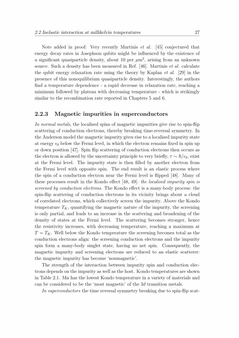
(a) (b) (c)
Figure 2.6: (a) The normalised differential conductance versus bias voltage for varyingconcentrations of Mn in Pb, showing the development of subgap states. Figure fromRef. [54]. (b) The differential conductance for various temperatures of a Cu layer withCr atoms, proximitised by a Pb layer; at low temperatures the subgap states inside thegap can be clearly resolved. (c) These states are well described by the Zittartz, Bringerand Muller-Hartmann (ZBMH) theory. Figure from Ref. [55].
tering leads to Cooper pair breaking, altering the superconducting state. An
increase of pair breakers leads to a decrease of the mean field parameters such
as the critical temperature and superconducting gap [51]. In addition, the pair-
ing potential and quasiparticle energy gap no longer are the same (without pair
breaking, both are set by the value of ∆), giving rise to gapless superconductivity
[6]. The Kondo effect gives rise to impurity bound states below the gap, which
form a band of subgap states with increasing impurity concentration [52, 53]. This
band of subgap states has been found experimentally in a variety of systems, for
example in Pb with Mn, and in proximitised structures, see Fig. 2.6, and can be
well described by the theory by Zittartz, Bringer and Muller-Hartmann [56].
Table 2.1: Kondo temperatures (in Kelvin) for 3d transition metals in common metals[50].
HostImpurity Cr Mn Fe
Cu 1.0 0.01 25
Ag ∼ 0.02 0.04 ∼ 3
Au ∼ 0.01 < 0.01 0.3
Al 1200 530 > 5000
2.2 Inelastic interaction at millikelvin temperatures 29
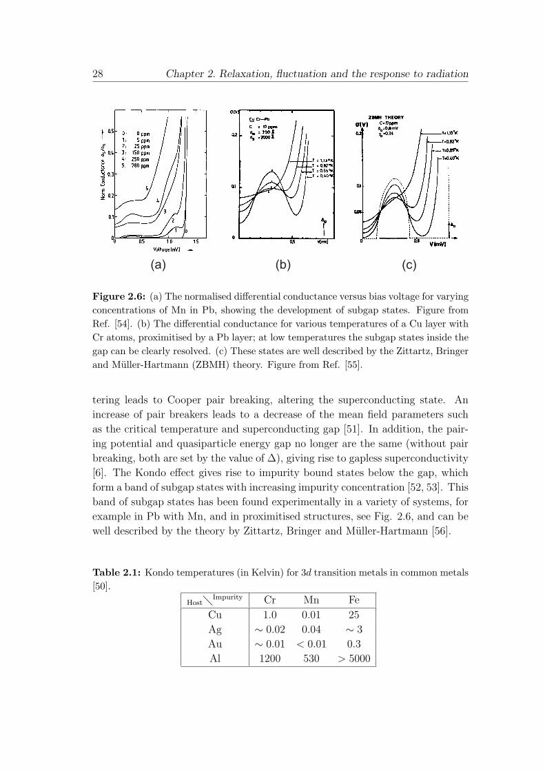
Figure 2.7: The differential conductance measured over a single Mn atom placed onNb using scanning tunnelling microscopy. The left figure shows the conductance overbare Nb and over the Mn atom, the difference for various distances is shown in theright figure. Very locally, within a nanometer around the Mn atom, a clear asymmetryis observed in the conductance. Figure from Ref. [58].
An interesting contradiction arises at very low temperatures: In supercon-
ductors all electrons are paired and the Cooper pairs, having no net spin, are
unable to screen the impurity; this while in normal metals the impurity is so well
screened it is effectively nonmagnetic. This issue was addressed by Sakurai [57],
who showed that in the presence of a strong (ε0 ¿ ∆) magnetic impurity the
groundstate changes, containing a localised quasiparticle to screen the impurity.
Quasiparticles in superconductors, Bogoliubov quasiparticles, are superpositions
of electrons and holes. Normally in a superconductor both are favoured equally
as a function of excitation energy (one exception is charge imbalance), see Ref.
[6]: the differential conductance is therefore symmetric around the Fermi level.
Interestingly, the changes in the groundstate imply particle-hole asymmetry on
a very local scale as well [58, 59]. These local changes are not included in the
impurity-averaged conventional pair breaking theories by Abrikosov and Gorkov,
as well as Zittartz, Bringer and Muller-Hartmann. In 1997 Yazdani et al. [58]
were the first to experimentally observe such a localised impurity bound state us-
ing scanning tunnelling microscopy over single Mn and Gd atoms placed on the
surface of Nb, see Fig. 2.7. The differential conductance shows clear deviations
within only a nanometer. Additionally, the differential conductance is asymmet-
ric, and is understood to arise from particle-hole asymmetry brought about by
the magnetic impurity [58, 59].
In Chapter 5 of this thesis we show a clear saturation of the quasiparticle
recombination time at low temperatures. This saturation is reminiscent to ex-

30 Chapter 2. Relaxation, fluctuation and the response to radiation
periments in normal metals which showed that at low temperatures timescales for
quasiparticles are limited by dilute concentrations of magnetic impurities, most
notably the inelastic electron-electron scattering (see Chapter 2.2.1). By analogy,
we have hypothesized that low temperature recombination in superconductors
could be related to magnetic impurities in the superconducting film. Modifica-
tions of the recombination time could arise from the alterations of the supercon-
ducting state such as the subgap states (related to possible quasiparticle traps
[44]), the groundstate quasiparticles, the influence of the magnetic moment on
the interactions between quasiparticles, as well as a possible spin-lattice coupling
[60]. In order to test whether recombination is related to magnetic impurities we
have implanted Mn in Ta and Al, see Chapter 6. We show that indeed the low
temperature relaxation time is strongly reduced by implantation, but that this
enhancement of the recombination process is not due to the magnetic moment,
but due to the enhancement of disorder, possibly involving surface defects with
magnetic moments.
2.3 Low frequency noise in superconducting sys-
tems
The counting of Cooper pairs and quasiparticles using superconducting resonators,
for photon detection or for elucidating physical processes, is fundamentally lim-
ited by particle number fluctuations. These particle number fluctuations arise
from the random generation of quasiparticles and their subsequent recombina-
tion. At the same time, other microscopic processes contribute to the noise of
superconducting resonators as well. Local dipoles in dielectrics in the active re-
gion of the resonator couple to the electric fields, possibly affecting the noise
properties. In addition, the time-varying orientation of magnetic moments, cou-
pling to the magnetic fields in the resonator, would contribute to the noise. These
three noise processes are apparent in the low frequency noise.
Interestingly, at low frequencies almost every system shows noise. Many sys-
tems with a 1/f or 1/f -like power spectral density have been found [61]. Low
frequency fluctuations have been encountered in SQUIDs, the most sensitive mag-
netometers [62], occur in everyday processes like the air temperature and wind
speed [63], and even have been found in the loudness of Bach’s first Brandenburg
concerto [64]! While 1/f noise is nearly ubiquitous it is nonuniversal, arising from
a variety of different physical processes [65]. In condensed matter physics, the
spectral shape of the noise is generally attributed to an ensemble of fluctuators
with a specific distribution of timescales: a 1/f noise spectrum can be generated

2.3 Low frequency noise in superconducting systems 31
by a particular superposition of Lorentzian spectra [61, 65, 66].
The superconducting resonators are ideal candidates for studying noise as they
are extremely sensitive: with quality factors reaching up to a million, they can
sense tiny fluctuations. At the same time, the results interest a broad community:
the noise processes we discuss above play an important role in the ongoing devel-
opments in photon detection and quantum information processing. Instead of an
obstacle to avoid, noise is a signal worth investigating. We start by introducing
the power spectral density, and discuss the three noise processes mentioned above
by reviewing recent advances in superconducting devices.
2.3.1 Power spectral density
The spectral properties of noise are described by the power spectral density [67],
which is given by the Fourier transform of the autocorrelation, as stated by the
Wiener-Khintchine theorem. This as the Fourier transform of a noise signal x(t)
is undefined because noise has infinite energy:∫∞−∞ |x(t)|2dt = ∞ (think of Parse-
val’s relation). This approach is valid when the noise process is strictly or weakly
stationary, i.e. its main properties are time-invariant. With the autocorrelation
given by Rx(t′) =< x(t)x∗(t− t′) >, the power spectral density Sx is
Sx(ω) ≡ 2F< x(t)x∗(t− t′) > (2.8)
It is twice the Fourier transform of the correlation function: Sx(ω) = 2Φx(ω).
The simplest example is a zero mean white noise process, where there is no
correlation between different time samples: it has an autocorrelation of Rx(t′) =
σ2x∆t′δ(t′), with ∆t′ a sampling time, giving a frequency independent spectrum
of Sx(ω) = 2σ2x∆t′, with σ2
x =< xx∗ > the variance; examples of such processes
include the Johnson noise in resistors at finite temperatures. On the other hand,
a Lorentzian spectrum is the hallmark of a noise process characterised by a single
timescale τ , such as for a two-level fluctuator [68]. With an autocorrelation given
by Rx(t′) =< xx∗ > e−|t
′|/τ , the power spectral density is
Sx(ω) = 2
∫ ∞
−∞σ2
xe−|t′|/τe−iωt′dt′ = 4σ2
x
∫ ∞
0
e−t′/τ cos(ωt′)dt′ =4σ2
xτ
1 + (ωτ)2(2.9)
forming a Lorentzian spectrum with a roll-off at a frequency reciprocal to the
characteristic timescale.
2.3.2 Particle number fluctuations
Particle number fluctuations in a superconductor arise from the spontaneous gen-
eration and recombination of quasiparticles, leading to generation-recombination
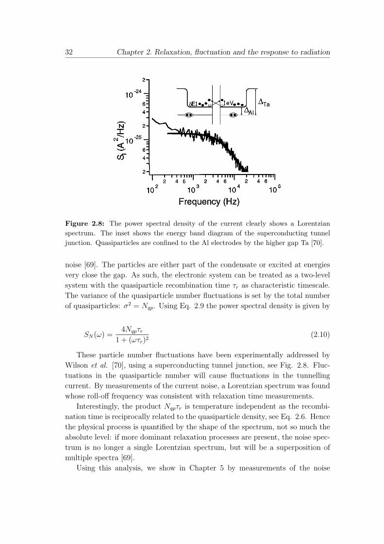
32 Chapter 2. Relaxation, fluctuation and the response to radiation
Figure 2.8: The power spectral density of the current clearly shows a Lorentzianspectrum. The inset shows the energy band diagram of the superconducting tunneljunction. Quasiparticles are confined to the Al electrodes by the higher gap Ta [70].
noise [69]. The particles are either part of the condensate or excited at energies
very close the gap. As such, the electronic system can be treated as a two-level
system with the quasiparticle recombination time τr as characteristic timescale.
The variance of the quasiparticle number fluctuations is set by the total number
of quasiparticles: σ2 = Nqp. Using Eq. 2.9 the power spectral density is given by
SN(ω) =4Nqpτr
1 + (ωτr)2(2.10)
These particle number fluctuations have been experimentally addressed by
Wilson et al. [70], using a superconducting tunnel junction, see Fig. 2.8. Fluc-
tuations in the quasiparticle number will cause fluctuations in the tunnelling
current. By measurements of the current noise, a Lorentzian spectrum was found
whose roll-off frequency was consistent with relaxation time measurements.
Interestingly, the product Nqpτr is temperature independent as the recombi-
nation time is reciprocally related to the quasiparticle density, see Eq. 2.6. Hence
the physical process is quantified by the shape of the spectrum, not so much the
absolute level: if more dominant relaxation processes are present, the noise spec-
trum is no longer a single Lorentzian spectrum, but will be a superposition of
multiple spectra [69].
Using this analysis, we show in Chapter 5 by measurements of the noise
2.3 Low frequency noise in superconducting systems 33
spectra under continuous optical illumination that the quasiparticle relaxation
process can be characterised by a single dominant timescale.
2.3.3 Flux noise
The existence of low temperature fluctuations in the magnetic flux has been
most apparent in experiments with superconducting quantum interference de-
vices (SQUIDs) [62]. SQUIDs consist of a superconducting ring with two tunnel
barriers, forming Josephson junctions; the current through the ring depends on
the phase-sensitive summation of the supercurrent passed by the two junctions
[6]. SQUIDS are extremely sensitive magnetometers as the phase depends on
the enclosed magnetic flux. Noise in the magnetic flux, flux noise, is presently
attracting increased attention as it is critical also for Josephson-based quantum
information processing. The noise has a 1/f -like spectrum, and is found to de-
pend only weakly on parameters like material and geometry. The origin of this
noise has thus far not been identified. Proposed flux noise mechanism include
electron spin locking in possible surface charge traps [71], interaction between
hypothesised surface magnetic moments due to conduction electrons [72], or dan-
gling bonds at for example the Si/SiO2 interface [73].
The insight in the origins of flux noise is evolving, as a set of recent, unre-
lated experiments is pointing towards the presence of magnetic moments on the
surfaces of superconducting films at low temperatures. Magnetic field-dependent
measurements of the critical current in superconducting Nb and MoGe nanowires
show a peak for nonzero fields [74], consistent with the paramagnetic ordering of
magnetic moments. The diameter dependence indicates a surface distribution of
magnetic moments. Scanning tunneling measurements on Nb show a V-shaped
differential conductance, pointing towards the presence of magnetic moments in
the native oxide [75]. Sendelbach et al. [76] have found the amount of excess
flux present in both Al and Nb SQUIDs to increase with decreasing tempera-
ture, whose strength depends on the field cooled flux density. These results are
consistent with the paramagnetic ordering of surface spins in the vortex cores
[77].
Surface spins are relevant for our case, as they would couple to the magnetic
fields in the resonator, appearing in the inductance. At the same time, magnetic
moments affect the superconducting state, possibly influencing quasiparticle re-
combination processes (see Chapter 2.2.3).
34 Chapter 2. Relaxation, fluctuation and the response to radiation
2.3.4 Dipole fluctuators
The permittivity of a dielectric arises from the combined atomic, molecular and
ionic frequency-dependent polarisability. Additionally, in disordered systems it
has become clear that a significant amount of configurational defects exists, fluc-
tuating between low lying energy states [78]. These two-level fluctuators are
apparent in measurements of the low temperature heat capacity, showing a peak
in the temperature dependence (this is known as the Schottky anomaly) [79].
Moreover, they bring about variations of the sound velocity and give rise to
acoustic attenuation in ultrasound experiments. Some of these fluctuators have
a dipole moment and respond to electric fields, affecting the real and imaginary
part of the complex permittivity ε, and by extension: the phase velocity and high
frequency absorptivity.
Amorphous systems are known to contain many defects, whose microscopic
origins vary, giving rise to dipole two-level systems [78]. Amorphous SiO2 for ex-
ample is known to contain many dipole defects [80, 81]; these can arise from the
flipping of the angles of the Si-O-Si bonds [82, 83], see inset Fig. 2.9a, the motion
of groups of molecules as well as defects related to oxygen vacancies [84]. Addi-
tionally, dipole defects are brought about by foreign molecules such as OH− ions
[81, 85]. These dipole fluctuators can described as a two-level system, represented
by a particle in a double well potential, see Fig. 2.9b; the characteristics, the en-
ergies and relaxation times, depend on the microscopic properties. The two-level
system fluctuates between the low-energy states, each having a different dipole
moment.
At low temperatures, where the frequency of the electromagnetic field is too
fast for relaxation, resonant interaction of the dipole two-level systems with the
electric field dominates, leading to a temperature dependence of the absolute
permittivity ε given by [78, 81]
δε
ε= −2p2P
ε
[Re Ψ
(1
2+
~ω2πikT
)− ln
(~ωkT
)](2.11)
with p the dipole moment, P the density of states and Ψ the digamma function.
In the limit kT > ~ω the above equation can be simplified to
δε
ε= −2p2P
εln
(T
T0
)(2.12)
with T0 an arbitrary reference temperature. At higher temperatures relaxational
interaction starts to dominate [81]. Fig. 2.9a shows such a temperature depen-
dence in permittivity data on SiOx.

2.3 Low frequency noise in superconducting systems 35
.01 0.1 1 10
Temperature (K)
-15
-10
-5
0
10
4de/e
En
erg
y
V
d
hW
2 E
(b)(a)
Figure 2.9: (a) The temperature dependence of the permittivity of amorphous SiO2
[86]. The solid line is Eq. 2.11. The inset shows the positions in SiO2 which canfluctuate in configuration [83]. (b) A particle in a double well potential: ~Ω/2 is thezero point energy, E is the energy difference between the states and V the potentialbarrier height.
Noise with a 1/f spectrum can result from a particular superposition of
Lorentzian spectra of dipole two-level systems: for a noise process due to thermal
activation, τ ∝ eE/kT , 1/f noise results from a flat distribution of fluctuators over
the energy [61, 65, 66]. The low frequency noise in the permittivity of dielectrics
in the active region of a resonator translates into noise in the resonance frequency.
2.3.5 Noise and frequency deviations in superconducting
resonators
One of the main themes of this thesis is the low temperature properties of super-
conducting resonators. In principle, these are determined by the superconductor,
but in practice these resonators exhibit a large amount of frequency noise as well
as deviations in the temperature dependence of the resonance frequency. A full
understanding of these phenomena is emerging, although not yet complete. Here,
we present an overview of the main experimental results thusfar and the proposed
interpretations by the Caltech group as well as by us.
We observe a clearly present nonmonotonicity in the temperature dependence
of the resonance frequency at low temperatures in superconducting resonators
36 Chapter 2. Relaxation, fluctuation and the response to radiation
made of Nb, Ta and Al on Si substrates [87, 88]. Gao et al. [89] find a similar
feature in Nb on sapphire resonators. Interestingly, we have recently found that
NbTiN on Si films do not show such a dependence. However, the nonmonotonicity
appears if we cover the NbTiN films with SiOx dielectric layers and increases
with the thickness of the layer. Both the data from Gao et al. [89] and our
experimental results can be accurately fitted with Eq. 2.11. This indicates that
dipole two-level systems distributed in the volume of dielectric layers give rise to
the observed nonmonotonicity.
The superconducting resonators show substantial frequency noise. Interest-
ingly, Gao et al. [90] find that the noise has a comparable level for a variety of
superconducting materials (Al, Nb) and dielectric substrates (Si, Ge, sapphire).
Moreover, the noise level depends on the power inside the resonator, following
S ∝ 1/P 0.5. The noise levels as well as the power dependence are comparable to
what we find in resonators of Al, Ta and NbTiN on Si substrates.
A challenge is to reduce the noise, which requires knowledge about the loca-
tion of the noise source as well as the physical mechanisms that cause the noise.
The Caltech group has conjectured that this frequency noise is due to fluctuating
two-level systems with a dipole moment, located in the dielectric materials, either
in the bulk of the substrate, the interfaces or the surfaces. In the proposed inter-
pretation the low temperature resonance frequency deviations with temperature
are coupled to the frequency noise via the temperature-dependent, time-varying
permittivity ε(r, t, T ) [89, 90, 91]. The peculiar power dependence of the noise
can then be explained by assuming the two-level systems are saturated due to
the high levels of electric fields used [91].
The noise also depends on the geometry, as the noise decreases with increasing
width of the transmission line. The experimentally observed scaling indicates that
the noise source is located on surfaces instead of in the bulk [91]. By increasing
the volume to surface ratio on the open end of the resonator, where the electric
fields are strongest, the noise can be significantly decreased [92].
Importantly, in Chapter 7 we find that the noise level of NbTiN on Si res-
onators increases as soon as SiOx is present, but remains unchanged with increas-
ing thickness, indicating that the noise is dominantly due to processes occurring
at interfaces. More specifically, the superconductor-dielectric interface or/and the
interface between the substrate and the sputtered dielectric layer. Additionally,
the noise levels we find in uncovered NbTiN are comparable to those in Ta and Al,
while the uncovered NbTiN does not show a nonmonotonicity. The noise results
indicate no direct coupling between frequency deviations with temperature and
frequency noise. Our results point towards the noise arising at interfaces, which
is in agreement with the measurements on the width dependence of the noise.

2.4 High frequency response of a superconducting film 37
The identification of the noise arising at the interfaces is an important step
towards using these resonators for photon detection. The noise can be decreased
by increasing the volume to surface ratio as well as by directly addressing the
interfaces. When optimising the geometry for photon detection the volume of the
central line is preferably kept small, as it acts as detector volume. In Chapter 8
we show that the noise decreases by almost an order of magnitude when widening
only the gaps of the resonator transmission line while keeping the central line the
same.
2.4 High frequency response of a superconduct-
ing film
The essential part of this thesis is probing the photo-induced changes in and
subsequent relaxation of the superconducting state; the variation in the Cooper
pair density and in the amount and distribution of quasiparticles over the energy
leads to a change in the high frequency response of the superconducting film.
This high frequency response is controlled by the complex conductivity.
Hallmarks of superconductivity are its zero resistance and its expulsion of
magnetic fields. Yet, the electromagnetic fields penetrate the surface with a
magnetic penetration depth λ, analogously to the skin depth in normal metals.
When applying a microwave signal the charge carriers ‘dance to the tune’: the
time-varying electric fields accelerate and decelerate both the Cooper pair con-
densate and the quasiparticle excitations. The quasiparticles scatter in much the
same way as normal electrons do, bringing about Ohmic dissipation, limiting the
real part of the conductivity. On the other hand, the non-dissipative, accelerative
response of the Cooper pairs leads to a kinetic inductance and imaginary part
of the conductivity. The electrodynamic response of the superconductor can be
treated as the superposition of the response of the condensate and the quasi-
particles, this is called the two-fluid model [6]. Applying the Drude model, the
real part of the conductivity is given by: σ1 = nne2τ/m, with nn the normal
electron density and τ the elastic scattering time; and the imaginary part is:
σ2 = nse2/mω, with ns the phenomenological superconducting electron density
[6]. These approximations are intuitive, relating variations in the quasiparticle
density nqp or superconducting electron density ns to changes in the complex
conductivity.
The electrodynamic response is controlled by two lengthscales: the magnetic
penetration depth λ and the coherence length ξ. When the coherence length is
much shorter than the penetration depth, ξ ¿ λ, the electromagnetic fields pretty
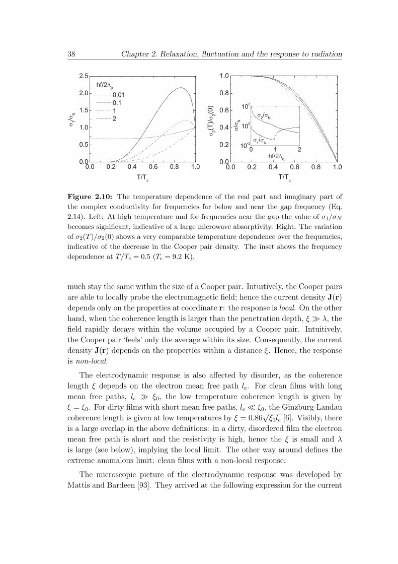
38 Chapter 2. Relaxation, fluctuation and the response to radiation
Figure 2.10: The temperature dependence of the real part and imaginary part ofthe complex conductivity for frequencies far below and near the gap frequency (Eq.2.14). Left: At high temperature and for frequencies near the gap the value of σ1/σN
becomes significant, indicative of a large microwave absorptivity. Right: The variationof σ2(T )/σ2(0) shows a very comparable temperature dependence over the frequencies,indicative of the decrease in the Cooper pair density. The inset shows the frequencydependence at T/Tc = 0.5 (Tc = 9.2 K).
much stay the same within the size of a Cooper pair. Intuitively, the Cooper pairs
are able to locally probe the electromagnetic field; hence the current density J(r)
depends only on the properties at coordinate r: the response is local. On the other
hand, when the coherence length is larger than the penetration depth, ξ À λ, the
field rapidly decays within the volume occupied by a Cooper pair. Intuitively,
the Cooper pair ‘feels’ only the average within its size. Consequently, the current
density J(r) depends on the properties within a distance ξ. Hence, the response
is non-local.
The electrodynamic response is also affected by disorder, as the coherence
length ξ depends on the electron mean free path le. For clean films with long
mean free paths, le À ξ0, the low temperature coherence length is given by
ξ = ξ0. For dirty films with short mean free paths, le ¿ ξ0, the Ginzburg-Landau
coherence length is given at low temperatures by ξ = 0.86√
ξ0le [6]. Visibly, there
is a large overlap in the above definitions: in a dirty, disordered film the electron
mean free path is short and the resistivity is high, hence the ξ is small and λ
is large (see below), implying the local limit. The other way around defines the
extreme anomalous limit: clean films with a non-local response.
The microscopic picture of the electrodynamic response was developed by
Mattis and Bardeen [93]. They arrived at the following expression for the current

2.4 High frequency response of a superconducting film 39
density,
Jω(r) = C
∫R[R ·Aω(r′)]
R4I(ω, R, f(E))e−R/ledr′ (2.13)
with R = r − r′, C a constant, A the vector potential, ω the radial frequency
and I(ω, R, f(E))e−R/le the response kernel. Both in the extreme anomalous
limit, where the response is non-local and I(ω, R, f(E)) has only a weak R-
dependence and drops out of the integral; as well as in the dirty limit, where the
response kernel can be approximated by a local response only, the integral can
be simplified. Then, the complex conductivity σ1 − iσ2, valid in the dirty and
extreme anomalous limit, is given by
σ1
σN
=2
~ω
∫ ∞
∆
[f(E)− f(E + ~ω)]g1(E)dE
+1
~ω
∫ −∆
∆−~ω[1− 2f(E + ~ω)]g1(E)dE
σ2
σN
=1
~ω
∫ ∆
max(∆−~ω,−∆)
[1− 2f(E + ~ω)]g2(E)dE
(2.14)
with
g1(E) =(1 + ∆2
E(E+~ω)
)NS(E)NS(E + ~ω)
g2(E) = E(E+~ω)+∆2√(E+~ω)2−∆2
√∆2−E2
= −ig1(E)(2.15)
The second part of the expression for σ1 is relevant for ~ω > 2∆; σn is the normal
state conductivity. The complex conductivity is controlled by the quasiparticle
energy distribution, density of states and energy gap, photon energy and case
II coherence factors, relevant for electromagnetic absorption [6]. For a thermal
distribution at temperature T , see Appendix B for the derivation, the above
equations can be simplified in the limit kT, ~ω < 2∆ to
σ1
σN
=4∆
~ωe−∆/kT sinh
(~ω2kT
)K0
(~ω2kT
)
σ2
σN
=π∆
~ω
[1− 2e−∆/kT e−~ω/2kT I0
(~ω2kT
)] (2.16)
with I and K modified Bessel functions of the first and second kind. The tem-
perature dependence of σ1 and σ2 is shown in Fig. 2.10.
For the local limit, the surface impedance is a direct result of Maxwell’s equa-
tions, giving for dirty limit thick films [95]
ZS =
√iµ0ω
σ1 − iσ2
= RS + iωLS (2.17)
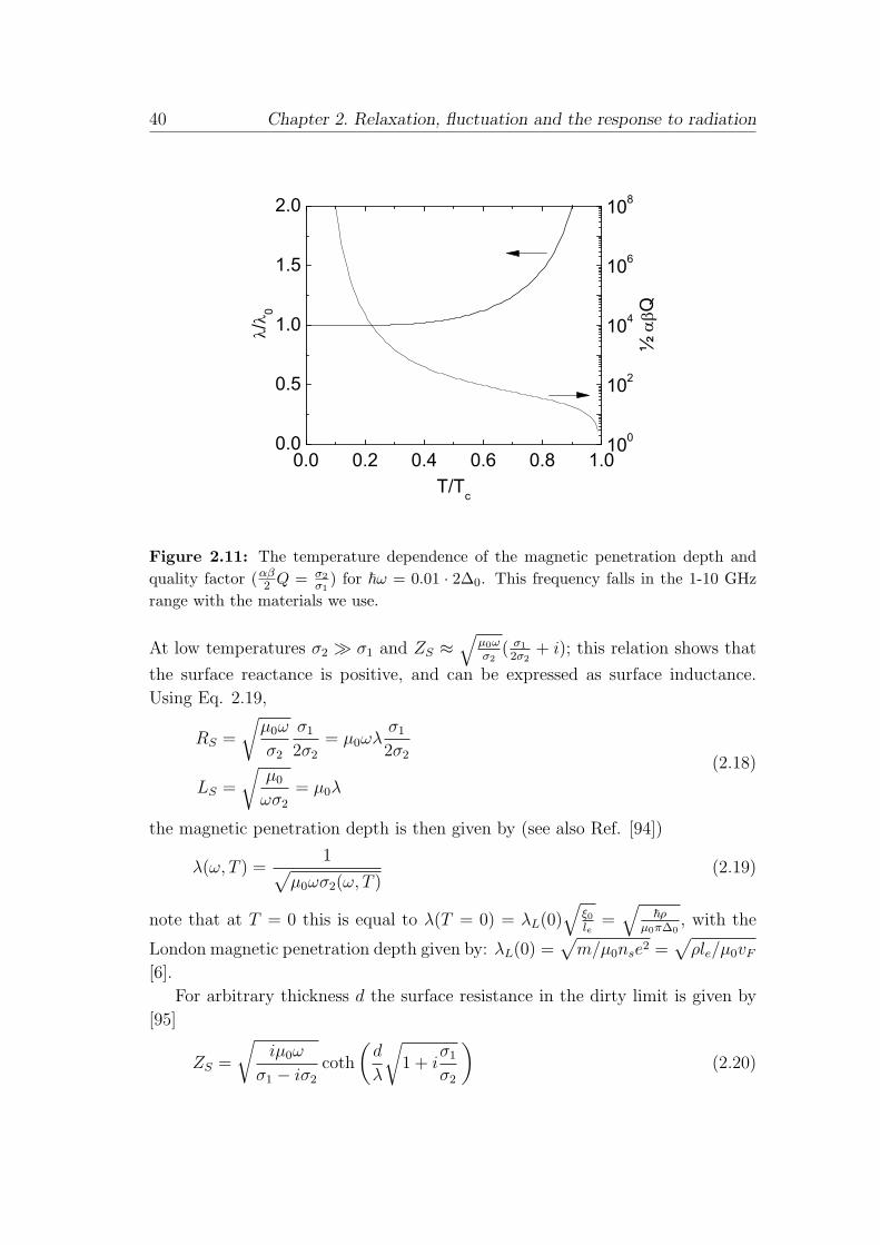
40 Chapter 2. Relaxation, fluctuation and the response to radiation
0.0 0.2 0.4 0.6 0.8 1.00.0
0.5
1.0
1.5
2.0
100
102
104
106
108
/0
T/Tc
½Q
Figure 2.11: The temperature dependence of the magnetic penetration depth andquality factor (αβ
2 Q = σ2σ1
) for ~ω = 0.01 · 2∆0. This frequency falls in the 1-10 GHzrange with the materials we use.
At low temperatures σ2 À σ1 and ZS ≈√
µ0ωσ2
( σ1
2σ2+ i); this relation shows that
the surface reactance is positive, and can be expressed as surface inductance.
Using Eq. 2.19,
RS =
√µ0ω
σ2
σ1
2σ2
= µ0ωλσ1
2σ2
LS =
õ0
ωσ2
= µ0λ
(2.18)
the magnetic penetration depth is then given by (see also Ref. [94])
λ(ω, T ) =1√
µ0ωσ2(ω, T )(2.19)
note that at T = 0 this is equal to λ(T = 0) = λL(0)√
ξ0le
=√
~ρµ0π∆0
, with the
London magnetic penetration depth given by: λL(0) =√
m/µ0nse2 =√
ρle/µ0vF
[6].
For arbitrary thickness d the surface resistance in the dirty limit is given by
[95]
ZS =
√iµ0ω
σ1 − iσ2
coth
(d
λ
√1 + i
σ1
σ2
)(2.20)
References 41
with λ the bulk value. For σ2 À σ1, using coth(x + iy) ' coth(x) − iysinh2(x)
for
y ¿ x,
RS = µ0ωλσ1
2σ2
β coth
(d
λ
)
LS = µ0λ coth
(d
λ
) (2.21)
with β = 1 + 2d/λsinh(2d/λ)
; for the bulk limit: β = 1, and for the thin film limit:
β = 2. The effective magnetic penetration depth for perpendicular fields is
λeff = λ coth( dλ), which has been experimentally verified [96]. Quality factors of
dirty limit superconducting cavities are then given by
Q =ωLtot
R=
1
α
ωLS
RS
=2
αβ
σ2
σ1
(2.22)
with α = LS/Ltot the fraction of kinetic to total (kinetic+geometric) inductance.
A variation in the complex conductivity leads to changes in the kinetic induc-
tance and quality factor
δLS
LS
= βδλ
λ= −β
2
δσ2
σ2
δQ
Q= −
(δσ1
σ1
− δσ2
σ2
) (2.23)
References
[1] N. W. Ashcroft and N. D. Mermin, Solid state physics, (Thomson Learning, 1976).
[2] D. Pines and P. Nozieres, The theory of quantum liquids I, (Addison-Wesley Pub-lishing Co., 1989).
[3] L. N. Cooper, Bound electron pairs in a degenerate Fermi gas, Phys. Rev. 104,1189 (1956).
[4] J. Bardeen, L. N. Cooper, and J. R. Schrieffer, Theory of superconductivity, Phys.Rev. 108, 1175 (1957).
[5] J. B. Ketterson and S. N. Song, Superconductivity, (Cambridge University Press,1999).
[6] M. Tinkham, Introduction to Superconductivity, (McGraw-Hill, New York, 1996).
[7] W. L. McMillan, Phys. Rev. 167, 331 (1968).
[8] H. Kamerlingh Onnes, Further experiments with liquid Helium. G. On the electri-cal resistance of pure metals, etc. VI. On the sudden change in the rate at whichresistance of mercury disappears, Comm. Phys. Lab. Univ. Leiden, No. 124C,1911.
42 Chapter 2. Relaxation, fluctuation and the response to radiation
[9] P. W. Anderson, Theory of dirty superconductors, J. Phys. Chem. Solids 11, 26(1959).
[10] J. J. Lin and J. P. Bird, Recent experimental studies of electron dephasing in metaland semiconductor mesoscopic structures, J. Phys.: Cond. Mat. 14, R501 (2002).
[11] P. Santhanam and D. E. Prober, Inelastic electron-scattering mechanisms in cleanaluminum films, Phys. Rev. B 29, 3733 (1984).
[12] M. Meschke, W. Guichard, and J. P. Pekola, Single-mode heat conduction byphotons, Nature 444, 187 (2006).
[13] H. Pothier, S. Gueron, Norman O. Birge, D. Esteve, and M. H. Devoret, EnergyDistribution Function of Quasiparticles in Mesoscopic Wires, Phys. Rev. Lett. 79,3490 (1997).
[14] B. L. Altshuler and A. G. Aronov in Electron-electron interactions in disorderedsystems, ed. by A. L. Efros and M. Pollak, (Elsevier, Amsterdam, 1985).
[15] B. Huard, Interactions between electrons, mesoscopic Josephson effect and asym-metric current fluctuations, Ph. D. Thesis, Pierre and Marie Curie University(2006).
[16] A. Anthore, F. Pierre, H. Pothier, and D. Esteve, Magnetic-field-dependent quasi-particle energy relaxation in mesoscopic wires, Phys. Rev. Lett. 90, 076806 (2003).
[17] F. Pierre, A. B. Gougam, A. Anthore, H. Pothier, D. Esteve, and N. O. Birge,Dephasing of electrons in mesoscopic metal wires, Phys. Rev. B 68, 085413 (2003).
[18] L. Saminadayar, P. Mohanty, R. A. Webb, P. Degiovanni, and C. Bauerle, Electroncoherence at low temperatures: The role of magnetic impurities, Physica E 40, 12(2007).
[19] B. Huard, A. Anthore, N. O. Birge, H. Pothier, and D. Esteve, Effect of magneticimpurities on energy exchange between electrons, Phys. Rev. Lett. 95, 036802(2005).
[20] A. Kaminski and L. I. Glazman, Electron Energy Relaxation in the Presence ofMagnetic Impurities, Phys. Rev. Lett. 86, 2400 (2001).
[21] T. Capron, Y. Niimi, F. Mallet, Y. Baines, D. Mailly, F. Y. Lo, A. Melnikov, A. D.Wieck, L. Saminadayar, and C. Bauerle, Low-temperature dephasing in irradiatedmetallic wires, Phys. Rev. B 77, 033102 (2008).
[22] Yu. N. Ovchinnikov and V. Z. Kresin, Nonstationary state of superconductors:Application to nonequilibrium tunneling detectors, Phys. Rev. B 58, 12416 (1998).
[23] A. G. Kozorezov, A. F. Volkov, J. K. Wigmore, A. Peacock, A. Poelaert, andR. den Hartog, Quasiparticle-phonon downconversion in nonequilibrium super-conductors, Phys. Rev. B 61, 11807 (2000).

References 43
[24] B. I. Miller and A. H. Dayem, Relaxation and recombination times of quasiparticlesin superconducting Al thin films, Phys. Rev. Lett. 18, 1000 (1967).
[25] J. R. Schrieffer and D. M. Ginsberg, Calculation of the Quasiparticle Recombina-tion Time in a Superconductor, Phys. Rev. Lett. 8, 207 (1962).
[26] D. M. Ginsberg, Upper Limit for Quasi-Particle Recombination Time in a Super-conductor, Phys. Rev. Lett. 8, 204 (1962).
[27] M. Reizer, Electron-electron relaxation in two-dimensional impure superconduc-tors, Phys. Rev. B 61, 7108 (2000).
[28] T. M. Klapwijk, P. A. van der Plas, and J. E. Mooij, Electron-electron scatteringin dirty three-dimensional aluminum films, Phys. Rev. B 33, 1474 (1986).
[29] S. B. Kaplan, C. C. Chi, D. N. Langenberg, J. J. Chang, S. Jafarey, and D. J.Scalapino, Quasiparticle and phonon lifetimes in superconductors, Phys. Rev. B14, 4854 (1976).
[30] B. Keck and A. Schmid, Superconductivity and electron-phonon interaction inimpure simple metals, J. Low Temp. Phys. 24, 611 (1976).
[31] V. F. Gantmakher, The experimental study of electron-phonon scattering in met-als, Rep. Prog. Phys. 37, 317 (1974).
[32] J. Rammer and A. Schmid, Destruction of phase coherence by electron-phononinteractions in disordered conductors, Phys. Rev. B 34, 1352 (1986).
[33] A. Sergeev and V. Mitin, Electron-phonon interaction in disordered conductors:Static and vibrating scattering potentials, Phys. Rev. B 61, 6041 (2000).
[34] E. M. Gershenzon, M. E. Gershenzon, G. N. Gol’tsman, A. M. Lyul’kin, A. D.Semenov, and A. V. Sergeev, Electron-phonon interaction in ultrathin Nb films,Sov. Phys. JETP 70, 505 (1990).
[35] M. E. Gershenson, D. Gong, T. Sato, B. S. Karasik, A. V. Sergeev, Millisecondelectronphonon relaxation in ultrathin disordered metal films at millikelvin tem-peratures, Appl. Phys. Lett. 79, 2049 (2001).
[36] J. Haust, M. Burst, R. Haueisen, and G. Weiss, Low temperature acoustic proper-ties of poly-crystalline aluminium, J. Low Temp. Phys. 137, 523 (2004).
[37] S. B. Kaplan, Acoustic matching of superconducting films to substrates, J. Low.Temp. Phys. 37, 343, (1979).
[38] A. Rothwarf and B. N. Taylor, Measurement of recombination lifetimes in super-conductors, Phys. Rev. Lett. 19, 27 (1967).
[39] K. E. Gray, Steady state measurements of the quasiparticle lifetime in supercon-ducting Al, J. Phys. F: Metal Phys. 1, 290 (1971).
44 Chapter 2. Relaxation, fluctuation and the response to radiation
[40] A. Peacock, P. Verhoeve, N. Rando, A. van Dordrecht, B. G. Taylor, C. Erd, M. A.C. Perryman, R. Venn, J. Howlett, D. J. Goldie, J. Lumley, and M. Wallis, Singleoptical photon detection with a superconducting tunnel junction, Nature 381, 135(1996).
[41] P. Verhoeve, R. den Hartog, A. G. Kozorezov, D. Martin, A. van Dordrecht, J. K.Wigmore, and A. Peacock, Time dependence of tunnel statistics and the energyresolution of superconducting tunnel junctions, J. Appl. Phys. 92, 6072 (2002).
[42] T. Nussbaumer, Ph. Lerch, E. Kirk, A. Zehnder, R. Fuchslin, P. F. Meier, andH. R. Ott, Quasiparticle diffusion in tantalum using superconducting tunnel junc-tions, Phys. Rev. B 61, 9719 (2000).
[43] L. Li, L. Frunzio, C. M. Wilson, and D. E. Prober, Quasiparticle nonequilibriumdynamics in a superconducting Ta film, J. Appl. Phys. 93, 1137 (2003).
[44] A. G. Kozorezov, J. K. Wigmore, A. Peacock, A. Poelaert, P. Verhoeve, R. denHartog, and G. Brammertz, Local trap spectroscopy in superconducting tunneljunctions, Appl. Phys. Lett. 78, 3654 (2001).
[45] J. M. Martinis, M. Ansmann and J. Aumentado, Energy Decay in JosephsonQubits from Non-equilibrium Quasiparticles, arXiv:0904.2171.
[46] M. D. Shaw, R. M. Lutchyn, P. Delsing, and P. M. Echternach, Kinetics ofnonequilibrium quasiparticle tunneling in superconducting charge qubits, Phys.Rev. B 78, 024503 (2008).
[47] P. W. Anderson, Localized magnetic states in metals, Phys. Rev. 124, 41 (1961).
[48] L. Kouwenhoven and L. Glazman, Revival of the Kondo effect, Physics World 14,33 (2001).
[49] J. Kondo, Resistance minimum in dilute magnetic alloys, Prog. Theoret. Phys.32, 37 (1964).
[50] D. K. Wohlleben and B. R. Coles, Formation of local moments in metals, inMagnetism vol. V, edited by H. Suhl, (Academic, New York, 1973).
[51] A. A. Abrikosov and L. P. Gorkov, Contribution to the theory of superconductingalloys with paramagnetic impurities, Sov. Phys. JETP 12, 1243 (1961).
[52] M. Brian Maple, Paramagnetic impurities in superconductors, in Magnetism vol.V, edited by H. Suhl, (Academic, New York, 1973).
[53] A. V. Balatsky, I. Vekhter, J. X. Zhu, Impurity-induced states in conventional andunconventional superconductors, Rev. Mod. Phys. 78, 373 (2006).
[54] W. Bauriedl, P. Ziemann, and W. Buckel, Electron-Tunneling Observation of Im-purity Bands in Superconducting Manganese-Implanted Lead, Phys. Rev. Lett. 47,1163 (1981).

References 45
[55] L. Dumoulin, E. Guyon, and P. Nedellec, Tunneling study of localized bands insuperconductors with magnetic impurities (normal Kondo alloys in the supercon-ducting proximity), Phys. Rev. B 16, 1086 (1977).
[56] J. Zittartz, A. Bringer, and E. Muller-Hartmann, Impurity bands in superconduc-tors with magnetic impurities, Solid State Comm. 10, 513 (1972).
[57] A. Sakurai, Comments on superconductors with magnetic impurities, Prog. The-oret. Phys. 44, 1472 (1970).
[58] A. Yazdani, B. A. Jones, C. P. Lutz, M. F. Crommie, and D. M. Eigler, Probingthe local effects of magnetic impurities on superconductivity, Science 275, 1767(1997).
[59] M. E. Flatte and J. M. Byers, Local electronic structure of defects in superconduc-tors, Phys. Rev. B 56, 11213 (1997).
[60] A. G. Kozorezov, A. A. Golubov, J. K. Wigmore, D. Martin, P. Verhoeve, R. A.Hijmering, and I. Jerjen, Inelastic scattering of quasiparticles in a superconductorwith magnetic impurities, Phys. Rev. B 78, 174501 (2008).
[61] P. Dutta and P. M. Horn, Low-frequency fluctuations in solids: 1/f noise, Rev.Mod. Phys. 53, 497 (1981).
[62] F. C. Wellstood, C. Urbina, and J. Clarke, Low-frequency noise in dc supercon-ducting quantum interference devices below 1 K, Appl. Phys. Lett. 50, 772 (1987).
[63] J. I. Yano, R. Blender, C. D. Zhang, and K. Fraedrich, 1/f noise and pulse-likeevents in the tropical atmospheric surface variabilities, Q. J. Royal Meteor. Soc.130, 1697 (2004).
[64] R. F. Voss and J. Clarke, 1/f noise in music and speech, Nature 258, 317 (1975).
[65] M. B. Weissman, 1/f noise and other slow, nonexponential kinetics in condensedmatter, Rev. Mod. Phys. 60, 537 (1988).
[66] C. C. Yu, Why study noise due to two level systems: a suggestion for experimen-talists, J. Low Temp. Phys. 137, 251 (2004).
[67] Sh. Kogan, Electronic noise and fluctuations in solids, (Cambridge UniversityPress, 1996).
[68] S. Machulp, Noise in semiconductors: spectrum of a two-parameter random signal,J. Appl. Phys. 25, 341 (1954).
[69] C. M. Wilson and D. E. Prober, Quasiparticle number fluctuations in supercon-ductors, Phys. Rev. B 69, 094524 (2004).
[70] C. M. Wilson, L. Frunzio, and D. E. Prober, Time-resolved measurements ofthermodynamic fluctuations of the particle number in a nondegenerate Fermi gas,Phys. Rev. Lett. 87, 067004 (2001).

46 Chapter 2. Relaxation, fluctuation and the response to radiation
[71] R. H. Koch, D. P. DiVincenzo, and J. Clarke, Model for 1/f flux noise in SQUIDsand qubits, Phys. Rev. Lett. 98, 267003 (2007).
[72] L. Faoro and L. B. Ioffe, Microscopic Origin of Low-Frequency Flux Noise inJosephson Circuits, Phys. Rev. Lett. 100, 227005 (2008).
[73] R. de Sousa, Dangling-bond spin relaxation and magnetic 1/f noise from theamorphous-semiconductor/oxide interface: Theory, Phys. Rev. B 76, 245306 (2007).
[74] A. Rogachev, T. C. Wei, D. Pekker, A. T. Bollinger, P. M. Goldbart, and A.Bezryadin, Magnetic-field enhancement of superconductivity in ultranarrow wires,Phys. Rev. Lett. 97, 137001 (2006).
[75] T. Proslier, J. F. Zasadzinski, L. Cooley, C. Antoine, J. Moore, J. Norem, M.Pellin, and K. E. Gray, Tunneling study of cavity grade Nb: Possible magneticscattering at the surface, Appl. Phys. Lett. 92, 212505 (2008).
[76] S. Sendelbach, D. Hover, A. Kittel, M. Muck, J. M. Martinis, and R. McDermott,Magnetism in SQUIDs at millikelvin temperatures, Phys. Rev. Lett. 100, 227006(2008).
[77] S. Sendelbach, D. Hover, A. Kittel, M. Mck, John M. Martinis, and R. McDermott,Calculations for magnetism in SQUIDs at millikelvin temperatures, arXiv:0802.1511.
[78] W. A. Phillips, Two-level states in glasses, Rep. Prog. Phys. 50, 1657 (1987).
[79] C. Kittel and H. Kroemer, Thermal physics, (Second Edition, W. H. Freeman andCompany, New York, 1997).
[80] B. Golding, M. von Schickfus, S. Hunklinger, and K. Dransfeld, Intrinsic electricdipole moment of tunneling systems in silica glasses, Phys. Rev. Lett. 43, 1817(1979).
[81] M. von Schickfus and S. Hunklinger, Dielectric coupling of low-energy excitationsin vitreous silica to electromagnetic waves, J. Phys. C: Solid State Phys. 9, L439(1976).
[82] J. Reinisch and A. Heuer, What Is Moving in Silica at 1 K? A Computer Studyof the Low-Temperature Anomalies, Phys. Rev. Lett. 95, 155502 (2005).
[83] C. Enss and S. Hunklinger, Low-Temperature Physics, (Springer Verlag, 2005).
[84] D. L. Griscom, Defect structure of glasses - some outstanding questions in regardto vitreous silica, J. Non-Crystalline Solids 73, 51 (1985).
[85] J. M. Martinis, K. B. Cooper, R. McDermott, M. Steffen, M. Ansmann, K. D.Osborn, K. Cicak, S. Oh, D. P. Pappas, R. W. Simmonds, and C. C. Yu, Deco-herence in Josephson Qubits from Dielectric Loss, Phys. Rev. Lett. 95, 210503(2005).
References 47
[86] M. Brandt, Einfluss von Kernquadrupolmomenten auf die Amplitude von Polar-isationsechos in amorphen Festkorpern, Ph. D. Thesis, University of Heidelberg(2004).
[87] R. Barends, J. J. A. Baselmans, J. N. Hovenier, J. R. Gao, S. J. C. Yates, T.M. Klapwijk, and H. F. C. Hoevers, Niobium and tantalum high Q resonators forphoton detectors, IEEE Trans. Appl. Sup. 17, 263 (2007).
[88] J. J. A. Baselmans, S. J. C. Yates, R. Barends, Y. J. Y. Lankwarden, J. R. Gao,H. F. C. Hoevers, and T. M. Klapwijk, Noise and sensitivity of aluminum kineticinductance detectors for sub-mm astronomy, J. Low Temp. Phys. 151, 524 (2008).
[89] J. Gao, M. Daal, A. Vayonakis, S. Kumar, J. Zmuidzinas, B. Sadoulet, B. A.Mazin, P. K. Day, and H. G. LeDuc, Experimental evidence for a surface distri-bution of two-level systems in superconducting lithographed microwave resonators,Appl. Phys. Lett. 92, 152505 (2008).
[90] J. Gao, J. Zmuidzinas, B. A. Mazin, H. G. LeDuc, and P. K. Day, Noise propertiesof superconducting coplanar waveguide microwave resonators, Appl. Phys. Lett.90, 102507 (2007).
[91] J. Gao, M. Daal, J. M. Martinis, A. Vayonakis, J. Zmuidzinas, B. Sadoulet, B. A.Mazin, P. K. Day, and H. G. LeDuc, A semiempirical model for two-level systemnoise in superconducting microresonators, Appl. Phys. Lett. 92, 212504 (2008).
[92] O. Noroozian, New resonator designs for reduced frequency noise in microwavekinetic inductance detectors, 2nd Workshop on the Physics and Applications ofSuperconducting Microresonators, SRON Utrecht, the Netherlands, 19-20 June,2008.
[93] D. C. Mattis and J. Bardeen, Theory of the anomalous skin effect in normal andsuperconducting metals, Phys. Rev. 111, 412 (1958).
[94] R. F. Broom and P. Wolf, Q factor and resonance amplitude of Josephson tunneljunctions, Phys. Rev. B, 16, 3100 (1977).
[95] R. L. Kautz, Picosecond pulses on superconducting striplines, J. Appl. Phys. 49,308 (1978).
[96] W. H. Henkels and C. J. Kircher, Penetration depth measurements on type IIsuperconductors, IEEE Trans. Magn. MAG-13, 63 (1977).

48 Chapter 2. Relaxation, fluctuation and the response to radiation
Chapter 3
Superconducting resonators
49
50 Chapter 3. Superconducting resonators
3.1 Introduction
Superconducting resonators are extremely sensitive probes due to their high qual-
ity factors. Quality factors reach values over 106, allowing for easily observing
fractional changes of less than a millionth in the complex conductivity or dielectric
permittivity. When used to probe the photo-induced changes in the supercon-
ducting state, these resonators become highly sensitive photon detectors. The
additional advantages are their large dynamic range and the natural possibility
for reading out large imaging arrays using frequency domain multiplexing. Planar
quarterwave or halfwave resonators can be easily fabricated. This versatile inno-
vation [1] was quickly picked up not only for photon detection [2, 3, 4] but also for
many more applications in condensed matter physics: resonators are used in all-
solid state circuit quantum information processing [5, 6], elucidating properties of
dielectrics [7], controlling nanomechanical oscillators [8], narrowband quantum-
limited Josephson microwave amplifiers [9], and frequency domain multiplexing
for transition edge sensor bolometers [10]. Alternatively, lumped-element res-
onators can be used, consisting of a tightly meandered superconducting line and
an interdigitated capacitor [11]. An advantage is that these resonators can be
used as polarisation sensitive absorbers at submillimeter frequencies. However,
their properties are coupled to the radiation absorption properties, complicating
optimisation. We therefore use straightforward planar quarterwave and halfwave
resonators.
The subject of this chapter is threefold: we describe the geometry and fabrica-
tion for realising these resonators, present the microwave properties for character-
ising these resonators, and provide a practical guide for probing these resonators.
In section 3.2 we address the design of these resonators. In section 3.3 we present
the microwave description for characterising these resonators, concluding with
convenient expressions for the scattering parameters and time domain observ-
ables. The fabrication process in discussed in section 3.4. We conclude in section
3.5 with a practical description of the cryogenic and room temperature setup as
well as an analysis of the setup noise level: the do’s and don’t’s in the cryostat
as well as the RF setup.
3.2 Design of a quarterwave resonator
3.2.1 A coplanar waveguide transmission line resonator
The microwave resonator, a distributed resonant circuit, consists of a transmission
line with a coupler annex open end at one side and at the other side a shorted
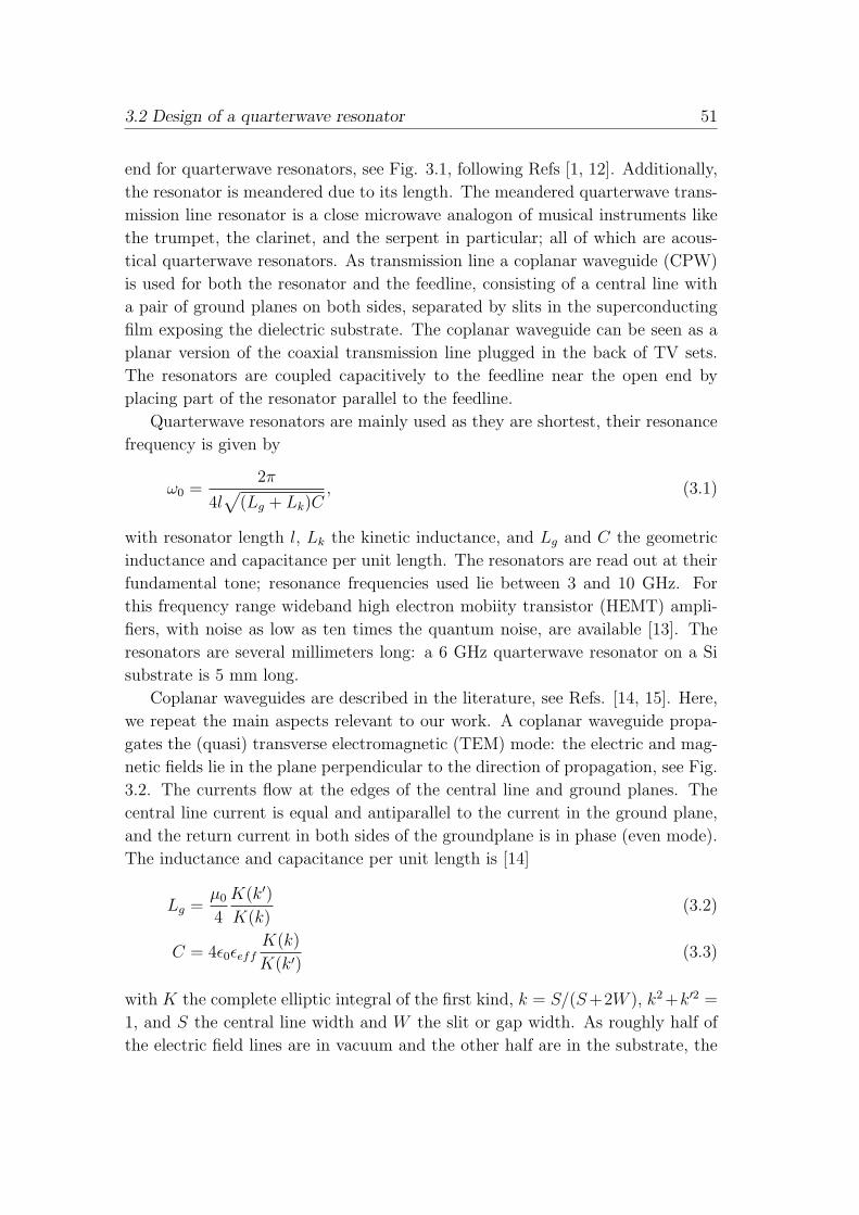
3.2 Design of a quarterwave resonator 51
end for quarterwave resonators, see Fig. 3.1, following Refs [1, 12]. Additionally,
the resonator is meandered due to its length. The meandered quarterwave trans-
mission line resonator is a close microwave analogon of musical instruments like
the trumpet, the clarinet, and the serpent in particular; all of which are acous-
tical quarterwave resonators. As transmission line a coplanar waveguide (CPW)
is used for both the resonator and the feedline, consisting of a central line with
a pair of ground planes on both sides, separated by slits in the superconducting
film exposing the dielectric substrate. The coplanar waveguide can be seen as a
planar version of the coaxial transmission line plugged in the back of TV sets.
The resonators are coupled capacitively to the feedline near the open end by
placing part of the resonator parallel to the feedline.
Quarterwave resonators are mainly used as they are shortest, their resonance
frequency is given by
ω0 =2π
4l√
(Lg + Lk)C, (3.1)
with resonator length l, Lk the kinetic inductance, and Lg and C the geometric
inductance and capacitance per unit length. The resonators are read out at their
fundamental tone; resonance frequencies used lie between 3 and 10 GHz. For
this frequency range wideband high electron mobiity transistor (HEMT) ampli-
fiers, with noise as low as ten times the quantum noise, are available [13]. The
resonators are several millimeters long: a 6 GHz quarterwave resonator on a Si
substrate is 5 mm long.
Coplanar waveguides are described in the literature, see Refs. [14, 15]. Here,
we repeat the main aspects relevant to our work. A coplanar waveguide propa-
gates the (quasi) transverse electromagnetic (TEM) mode: the electric and mag-
netic fields lie in the plane perpendicular to the direction of propagation, see Fig.
3.2. The currents flow at the edges of the central line and ground planes. The
central line current is equal and antiparallel to the current in the ground plane,
and the return current in both sides of the groundplane is in phase (even mode).
The inductance and capacitance per unit length is [14]
Lg =µ0
4
K(k′)K(k)
(3.2)
C = 4ε0εeffK(k)
K(k′)(3.3)
with K the complete elliptic integral of the first kind, k = S/(S+2W ), k2 +k′2 =
1, and S the central line width and W the slit or gap width. As roughly half of
the electric field lines are in vacuum and the other half are in the substrate, the
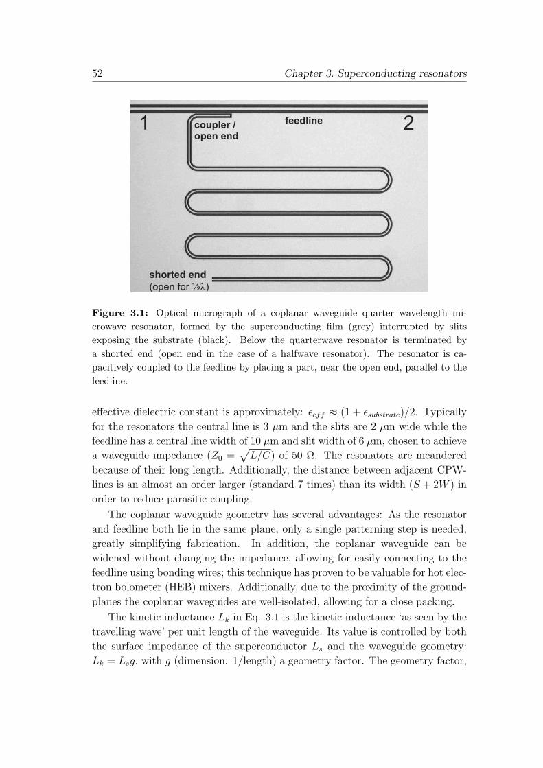
52 Chapter 3. Superconducting resonators
1 2
shorted end
(open for ½ )l
coupler /open end
feedline
Figure 3.1: Optical micrograph of a coplanar waveguide quarter wavelength mi-crowave resonator, formed by the superconducting film (grey) interrupted by slitsexposing the substrate (black). Below the quarterwave resonator is terminated bya shorted end (open end in the case of a halfwave resonator). The resonator is ca-pacitively coupled to the feedline by placing a part, near the open end, parallel to thefeedline.
effective dielectric constant is approximately: εeff ≈ (1 + εsubstrate)/2. Typically
for the resonators the central line is 3 µm and the slits are 2 µm wide while the
feedline has a central line width of 10 µm and slit width of 6 µm, chosen to achieve
a waveguide impedance (Z0 =√
L/C) of 50 Ω. The resonators are meandered
because of their long length. Additionally, the distance between adjacent CPW-
lines is an almost an order larger (standard 7 times) than its width (S + 2W ) in
order to reduce parasitic coupling.
The coplanar waveguide geometry has several advantages: As the resonator
and feedline both lie in the same plane, only a single patterning step is needed,
greatly simplifying fabrication. In addition, the coplanar waveguide can be
widened without changing the impedance, allowing for easily connecting to the
feedline using bonding wires; this technique has proven to be valuable for hot elec-
tron bolometer (HEB) mixers. Additionally, due to the proximity of the ground-
planes the coplanar waveguides are well-isolated, allowing for a close packing.
The kinetic inductance Lk in Eq. 3.1 is the kinetic inductance ‘as seen by the
travelling wave’ per unit length of the waveguide. Its value is controlled by both
the surface impedance of the superconductor Ls and the waveguide geometry:
Lk = Lsg, with g (dimension: 1/length) a geometry factor. The geometry factor,
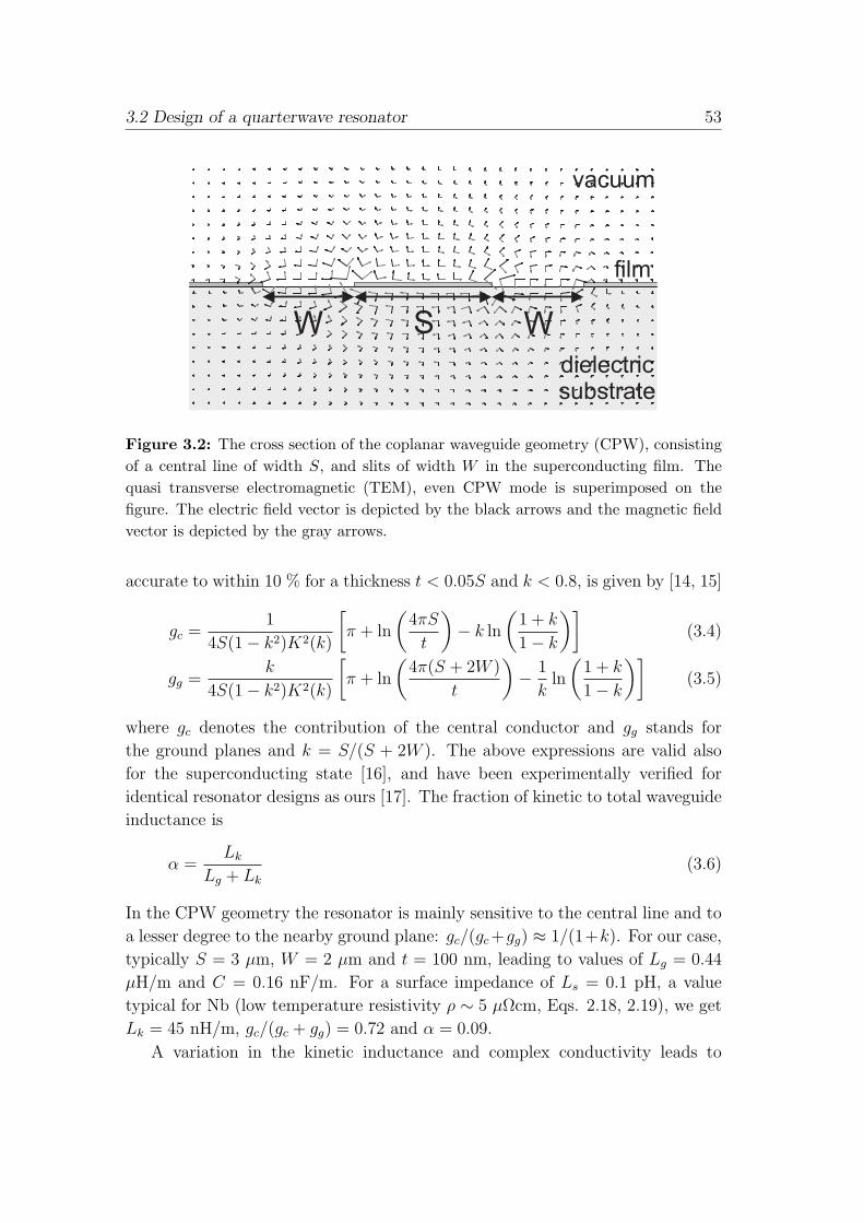
3.2 Design of a quarterwave resonator 53
S WW
dielectric
substrate
vacuum
film
Figure 3.2: The cross section of the coplanar waveguide geometry (CPW), consistingof a central line of width S, and slits of width W in the superconducting film. Thequasi transverse electromagnetic (TEM), even CPW mode is superimposed on thefigure. The electric field vector is depicted by the black arrows and the magnetic fieldvector is depicted by the gray arrows.
accurate to within 10 % for a thickness t < 0.05S and k < 0.8, is given by [14, 15]
gc =1
4S(1− k2)K2(k)
[π + ln
(4πS
t
)− k ln
(1 + k
1− k
)](3.4)
gg =k
4S(1− k2)K2(k)
[π + ln
(4π(S + 2W )
t
)− 1
kln
(1 + k
1− k
)](3.5)
where gc denotes the contribution of the central conductor and gg stands for
the ground planes and k = S/(S + 2W ). The above expressions are valid also
for the superconducting state [16], and have been experimentally verified for
identical resonator designs as ours [17]. The fraction of kinetic to total waveguide
inductance is
α =Lk
Lg + Lk
(3.6)
In the CPW geometry the resonator is mainly sensitive to the central line and to
a lesser degree to the nearby ground plane: gc/(gc +gg) ≈ 1/(1+k). For our case,
typically S = 3 µm, W = 2 µm and t = 100 nm, leading to values of Lg = 0.44
µH/m and C = 0.16 nF/m. For a surface impedance of Ls = 0.1 pH, a value
typical for Nb (low temperature resistivity ρ ∼ 5 µΩcm, Eqs. 2.18, 2.19), we get
Lk = 45 nH/m, gc/(gc + gg) = 0.72 and α = 0.09.
A variation in the kinetic inductance and complex conductivity leads to
54 Chapter 3. Superconducting resonators
changes in the resonance frequency, using Eqs. 3.1 and 2.23
δω0
ω0
= −α
2
δLk
Lk
=αβ
4
δσ2
σ2
(3.7)
3.2.2 Coupling
The resonators are coupled capacitively to the feedline near the open end, by
running a part of the resonator CPW-line alongside the feedline, while keeping
the ground plane uninterrupted. An uninterrupted groundplane is imperative,
otherwise the current path on one side of the groundplane differs from the other
one, and undesired odd modes can arise due to the phase difference: the return
current in both sides of the groundplane is no longer in phase. The quality factor
is defined as the energy in the system over the energy lost per cycle
Q =ωE
P(3.8)
In our case, the coupler can be seen as a 3 port system: port 1 and port 2
are the left and right side of the feedline (see Fig. 3.1) and port 3 is at the
resonator waveguide just under the coupler. Per cycle, i.e. two round-trips along
the resonator waveguide, the travelling wave encounters the coupler twice and
energy is leaked from port 3 into port 1 and 2: P = 2fE(|S13|2 + |S23|2), with S13
the scattering matrix element denoting the voltage transmission from port 3 to
1. A quarterwave resonator also accommodates higher order modes: nλ/4 with
n = 1, 3, 5, 7 etc. Per cycle the coupler is encountered 2/n times. As S13 = S23,
the coupling quality factor is given by
Qc =nπ
2|S13|2 (3.9)
with n = 1 for the quarter wavelength mode. The numerical value of S13 can be
calculated using microwave simulation software, see Ref. [12] for details. Increas-
ing the length or decreasing the distance to the feedline decreases the coupling
quality factor.
The quality factor of the loaded resonator is given by
1
Ql
=1
Qc
+1
Qi
(3.10)
with Qi denoting the internal, or unloaded quality factor. It reflects the losses in
the superconductor (Eq. 2.22), in the dielectric, or the radiation losses [12]. The
response time of the resonator is given by τres = Ql/πf0.

3.3 Microwave perspective on a superconducting resonator 55
3.3 Microwave perspective on a superconduct-
ing resonator
In this section we consider the microwave behaviour of the resonator. We derive
the scattering parameters, address the resonance circle, and define the obervables,
phase θ and amplitude A, which are used to sense the resonator in the time
domain. In addition we consider the power levels inside the resonator. While we
focus on quarterwave resonators in this section, the analysis is valid also for both
halfwave resonators and higher order modes.
3.3.1 Scattering parameters
In essence, a quarterwave resonator is a piece of transmission line with an open
end on one and a shorted end on the other side. Applying the telegraph equation,
a transmission line has a characteristic impedance of [18]
Z0 =
√R + iωL
G + iωC≈
√L
C(3.11)
with L and C the inductance and capacitance per unit length, and R the dis-
tributed resistance of the transmission line and G the conductance of the di-
electric, both contributing to the losses. The complex propagation constant is
γ =√
(R + iωL)(G + iωC) = α + iβ (3.12)
with α ' 12(R/Z0 + GZ0) the attenuation constant and β ' ω
√LC = ω/v, here
v = 1/√
LC is the phase velocity. The impedance of a shorted transmission line
resonator (i.e. terminated with a zero load) with characteristic impedance Z0 is
[18]
ZTLR = Z0 tanh(γl) = Z01− i tanh(αl) cot(βl)
tanh(αl)− i cot(βl)(3.13)
The internal quality factor of an unloaded resonator is Qi = β2α
. Using l = 14λ,
near resonance: βl = π2(1 + δω
ω), coth(βl) ≈ −π
2δωω
and tanh(αl) ≈ 12Qi
π2(1 + δω
ω).
The unloaded resonator resonates at a frequency ω1/4, which takes both geometry,
dielectrics and kinetic inductance into account:δω1/4
ω1/4=
ω−ω1/4
ω1/4. Putting it all
together and simplifying results in
ZTLR = Z04Qi/π
1 + i2Qiδω1/4
ω1/4
= Z0
4Qi
π− i
8Q2i
π
δω1/4
ω1/4
1 + 4Q2i (
δω1/4
ω1/4)2
(3.14)
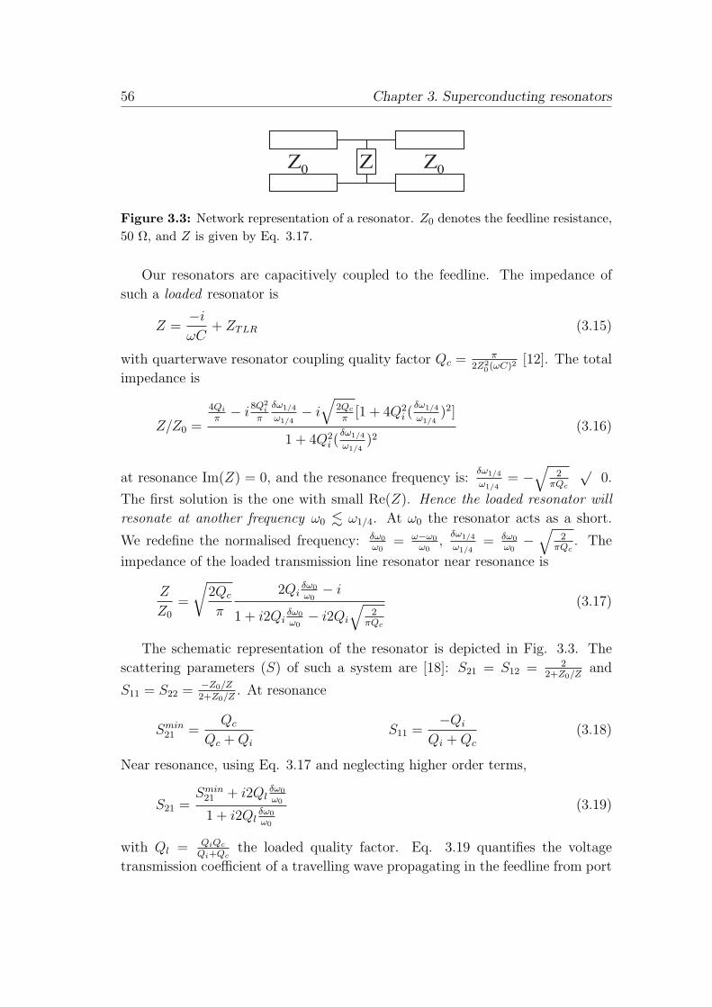
56 Chapter 3. Superconducting resonators
ZZ0
Z0
Figure 3.3: Network representation of a resonator. Z0 denotes the feedline resistance,50 Ω, and Z is given by Eq. 3.17.
Our resonators are capacitively coupled to the feedline. The impedance of
such a loaded resonator is
Z =−i
ωC+ ZTLR (3.15)
with quarterwave resonator coupling quality factor Qc = π2Z2
0 (ωC)2[12]. The total
impedance is
Z/Z0 =
4Qi
π− i
8Q2i
π
δω1/4
ω1/4− i
√2Qc
π[1 + 4Q2
i (δω1/4
ω1/4)2]
1 + 4Q2i (
δω1/4
ω1/4)2
(3.16)
at resonance Im(Z) = 0, and the resonance frequency is:δω1/4
ω1/4= −
√2
πQc
√0.
The first solution is the one with small Re(Z). Hence the loaded resonator will
resonate at another frequency ω0 . ω1/4. At ω0 the resonator acts as a short.
We redefine the normalised frequency: δω0
ω0= ω−ω0
ω0,
δω1/4
ω1/4= δω0
ω0−
√2
πQc. The
impedance of the loaded transmission line resonator near resonance is
Z
Z0
=
√2Qc
π
2Qiδω0
ω0− i
1 + i2Qiδω0
ω0− i2Qi
√2
πQc
(3.17)
The schematic representation of the resonator is depicted in Fig. 3.3. The
scattering parameters (S) of such a system are [18]: S21 = S12 = 22+Z0/Z
and
S11 = S22 = −Z0/Z2+Z0/Z
. At resonance
Smin21 =
Qc
Qc + Qi
S11 =−Qi
Qi + Qc
(3.18)
Near resonance, using Eq. 3.17 and neglecting higher order terms,
S21 =Smin
21 + i2Qlδω0
ω0
1 + i2Qlδω0
ω0
(3.19)
with Ql = QiQc
Qi+Qcthe loaded quality factor. Eq. 3.19 quantifies the voltage
transmission coefficient of a travelling wave propagating in the feedline from port
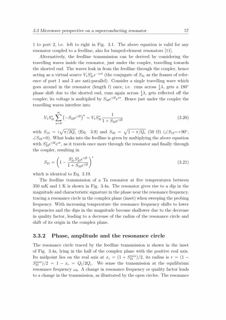
3.3 Microwave perspective on a superconducting resonator 57
1 to port 2, i.e. left to right in Fig. 3.1. The above equation is valid for any
resonator coupled to a feedline, also for lumped-element resonators [11].
Alternatively, the feedline transmission can be derived by considering the
travelling waves inside the resonator, just under the coupler, travelling towards
the shorted end. The waves leak in from the feedline through the coupler, hence
acting as a virtual source V1S∗31e
−iωt (the conjugate of S31 as the frames of refer-
ence of port 1 and 3 are anti-parallel). Consider a single travelling wave which
goes around in the resonator (length l) once, i.e. runs across 14λ, gets a 180
phase shift due to the shorted end, runs again across 14λ, gets reflected off the
coupler; its voltage is multiplied by S33eγ2leiπ. Hence just under the coupler the
travelling waves interfere into
V1S∗31
∞∑n=0
(−S33eγ2l
)n= V1S
∗31
1
1 + S33eγ2l(3.20)
with S13 = i√
π/2Qc (Eq. 3.9) and S33 =√
1− π/Qc (50 Ω) (∠S13=+90,∠S33=0). What leaks into the feedline is given by multiplying the above equation
with S∗23eγ2leiπ, as it travels once more through the resonator and finally through
the coupler, resulting in
S21 =
(1− S∗31S
∗23e
γ2l
1 + S33eγ2l
)∗(3.21)
which is identical to Eq. 3.19.
The feedline transmission of a Ta resonator at five temperatures between
350 mK and 1 K is shown in Fig. 3.4a. The resonator gives rise to a dip in the
magnitude and characteristic signature in the phase near the resonance frequency,
tracing a resonance circle in the complex plane (inset) when sweeping the probing
frequency. With increasing temperature the resonance frequency shifts to lower
frequencies and the dips in the magnitude become shallower due to the decrease
in quality factor, leading to a decrease of the radius of the resonance circle and
shift of its origin in the complex plane.
3.3.2 Phase, amplitude and the resonance circle
The resonance circle traced by the feedline transmission is shown in the inset
of Fig. 3.4a, lying in the half of the complex plane with the positive real axis.
Its midpoint lies on the real axis at xc = (1 + Smin21 )/2, its radius is r = (1 −
Smin21 )/2 = 1 − xc = Ql/2Qc. We sense the transmission at the equilibrium
resonance frequency ω0. A change in resonance frequency or quality factor leads
to a change in the transmission, as illustrated by the open circles. The resonance
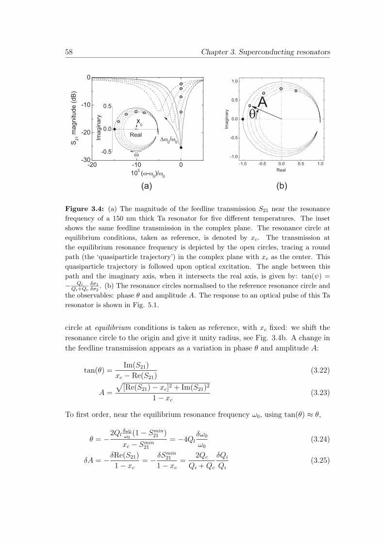
58 Chapter 3. Superconducting resonators
-20 -10 0-30
-20
-10
0
1
-0.5
0.0
0.5
Ima
gin
ary
Real
w
xc
Dw0/w
0S21
ma
gn
itu
de
(dB
)
105(w-w
0)/w
0
(a) (b)
Figure 3.4: (a) The magnitude of the feedline transmission S21 near the resonancefrequency of a 150 nm thick Ta resonator for five different temperatures. The insetshows the same feedline transmission in the complex plane. The resonance circle atequilibrium conditions, taken as reference, is denoted by xc. The transmission atthe equilibrium resonance frequency is depicted by the open circles, tracing a roundpath (the ‘quasiparticle trajectory’) in the complex plane with xc as the center. Thisquasiparticle trajectory is followed upon optical excitation. The angle between thispath and the imaginary axis, when it intersects the real axis, is given by: tan(ψ) =− Qi
Qi+Qc
δσ1δσ2
. (b) The resonance circles normalised to the reference resonance circle andthe observables: phase θ and amplitude A. The response to an optical pulse of this Taresonator is shown in Fig. 5.1.
circle at equilibrium conditions is taken as reference, with xc fixed: we shift the
resonance circle to the origin and give it unity radius, see Fig. 3.4b. A change in
the feedline transmission appears as a variation in phase θ and amplitude A:
tan(θ) =Im(S21)
xc − Re(S21)(3.22)
A =
√[Re(S21)− xc]2 + Im(S21)2
1− xc
(3.23)
To first order, near the equilibrium resonance frequency ω0, using tan(θ) ≈ θ,
θ = −2Qlδω0
ω0(1− Smin
21 )
xc − Smin21
= −4Qlδω0
ω0
(3.24)
δA = −δRe(S21)
1− xc
= − δSmin21
1− xc
=2Qc
Qi + Qc
δQi
Qi
(3.25)

3.3 Microwave perspective on a superconducting resonator 59
where for θ the minus sign arises from the fact that under operation the resonator
is continuously probed at the equilibrium value of ω0, and the path in the complex
plane for decreasing resonance frequency is opposite to the the path for increasing
probing frequency ω. When only the complex conductivity is concerned, using
Eqs. 2.23 and 3.7, θ and A become
θ = −αβQlδσ2
σ2
(3.26)
A = 1− 2Ql
Qi
(δσ1
σ1
− δσ2
σ2
). (3.27)
Accordingly, both θ and A are probes for the complex conductivity. The choice
for θ and A as observables allows for easily comparing different resonators due to
the normalisation. Additionally, the contribution of the system to the on and off
resonance noise is identical in both cases.
3.3.3 Probing signal power
Here we derive the power as well as the electric field strength at resonance.
Suppose we have a 3 port network, port 1 is input, port 2 is output and port 3 is
just under the resonator coupler, see Fig. 3.1. A travelling wave with amplitude
V1 travels from 1 to 2, and undergoes destructive interference, as such that at port
2 the amplitude is only V1S21. The travelling wave from the resonator travelling
towards the coupler has amplitude V3. The decrease in V1 is largely due to the
signal travelling from port 3 to 2 (V3S23), being exactly out of phase, and to a
smaller degree due to part of the signal travelling from port 1 to port 3 (V1S31).
Hence,
V1S21 = V1(1− S31)− V3S23 (3.28)
V3
V1
=Ql
Qc
√2Qc
π− 1 (3.29)
Pinternal
Preadout
=V 2
3 /Zresonator
V 21 /Zfeedline
∼= 2
π
Q2l
Qc
Zfeedline
Zresonator
(3.30)
with Pinternal the power of the travelling wave inside the resonator (not the stand-
ing wave) and for the same transmission line impedance. The forward and back-
ward travelling wave interfere into a standing wave which has an amplitude of
Vr = 2V3 (root mean square voltage). Typically for the characteristic impedance:
Zresonator = Zfeedline = 50 Ω.
The energy inside is
2
∫ l
0
1
2C
[Vr sin
(2π
4lx
)]2
dx =1
2CV 2
r l (3.31)
60 Chapter 3. Superconducting resonators
with C the capacitance per unit length of the CPW. The factor 2 in front is
because the same amount of energy resides in the inductance at resonance. To
give an example: consider applying -90 dBm in the feedline, i.e. 1 pW readout
power, to a resonator on a Si substrate (εsubstrate = 11.9) with Qi = 106, Qc = 105,
fres = 10 GHz, l = 2.95 mm, with a central line width of 3 µm and gap width
of 2 µm, giving C = 165 pF/m (Eq. 3.3). The internal resonator power becomes
Pinternal=-43 dBm, giving V3 = 1.6 mV (Pinternal = V 23 /Zresonator), and Vr = 3.2
mV. The electric field strength results in E = 1.6 kV/m near the open end. The
energy inside the resonator is 2.6 aJ, equal to 3.9 · 105 photons.
3.4 Sample fabrication
Fabrication starts with the deposition of a superconducting film on a cleaned Si
or sapphire wafer. In general, we use (100)-oriented Si (purchased from Topsil
Semiconductor Materials A/S) with a room temperature resistivity in excess of 1
kΩcm or in excess of 10 kΩcm. Prior to deposition, the wafer is dipped into HF to
remove the native oxide and passivate the dangling bonds on the Si surface with
hydrogen. We believe the oxide to be detrimental to the resonator properties,
hence this step is crucial: silicon oxide is known to contain many defects [19],
giving rising to possible electron trapping states [20] as well as dipole two-level
systems [21]. Additionally, the dangling bonds in the Si/SiO2 interface have been
suggested to lead to flux noise in Josephson flux qubits [22]. The sapphire (from
UniversityWafers.com) used for the samples described in this thesis is A-plane
oriented.
The superconducting resonators used in this thesis are made of Al, Ta, Nb or
NbTiN. The Nb and NbTiN films have been DC sputter deposited in the Nordiko
sputtering system at Delft University of Technology. The Nb has also been used as
counterelectrodes in the superconductor-insulator-superconductor (SIS) junctions
fabricated in our group, and the NbTiN has been used as part of the tuning
structure in Nb SIS junctions for HIFI band 3 and 4 of the Herschel space-based
observatory [23]. Patterning is done using photolithography and reactive ion
etching in a SF6/O2 plasma, using laser endpoint detection to avoid overetching
of the substrate. The Ta and Al samples are fabricated in the SRON cleanroom
in Utrecht. For the Ta samples used, prior to Ta DC sputter deposition, a 6 nm
Nb seed layer is deposited in situ to promote the growth of the desired body-
centered-cubic crystal orientation [24]. Subsequently the film is patterned using
photolithography and CF4/O2 reactive ion etching. The Al is evaporated or
sputtered and is patterned using photolithography and wet etching in a solution

3.5 Measurement techniques 61
of phosphoric acid, acetic acid and nitric acid. After fabrication the samples are
covered with a poly(methyl methacrylate) (PMMA) layer to protect them during
dicing, this layer is removed prior to measuring.
A wafer contains chips with resonators as well as chips with DC test devices.
The chips with resonators have dimensions of 20x4 mm, and typically contain
around 30-50 resonators. The DC test devices, with strips with varying widths,
are used to ascertain the DC properties of the film, i.e. the critical temperature,
resistivity and residual resistance ratio.
3.5 Measurement techniques
To reduce the density of quasiparticle excitations, for reaching high quality factors
and long relaxation times for photon detection, the samples need to be cooled
to below a tenth of the critical temperature; at temperatures between several
tens and hundreds of millikelvin. At the same time frequencies up to 10 GHz
are used, where impedance matching is not trivial. Care has to be taken to
ensure thermalisation of the cables while keeping the reflections to a minimum;
microwave and cryogenics are interwoven in the setup. The readout is done
using a signal generator, low noise amplifier, quadrature mixer and digitiser. The
quadrature mixer needs to be calibrated carefully. Additionally, possible ground
loops result in large spikes in the noise spectra. The unforgiving combination of
high frequencies, low temperatures and quadrature mixing makes a reliable, low
noise measurement setup a key ingredient.
3.5.1 Cryostat
We use a two-stage He-3 sorption cooler [25] inside a liquid He cryostat to reach
a base temperature of 310 mK. Inside the sorption cooler a porous material
(the sorption pump) releases He-3 when heated to about 40 K. The He-3 gas
subsequently liquefies as it passes a condenser, in contact with a pumped He-4
bath (the second stage), and trickles down onto the sample stage. When the
sorption pump is no longer heated it starts to absorb the He-3 and decrease the
vapour pressure. The sample stage is cooled by evaporative cooling. The sample
box is mounted on top of the He-3 sorption cooler, see Fig. 3.5. The samples
are glued into the sample box using GE varnish. Several sample box lids are
coated on the inside with a mixture of stycast and 1 mm SiC grains to form a
blackbody [26] in order to absorb stray photons entering the sample box. We
find that the amplitude of the response to optical pulses is reduced by over 90 %
when using coated lids, indicating their effectiveness. We find no effect on the

62 Chapter 3. Superconducting resonators
RF signal in
Sample box
RF signal out
Low noise amplifier
3He sorption cooler
Magnetic shield
GaAsP LED
(1.9 eV)
Figure 3.5: The cryostat used in Delft, showing the 4.2 K cold plate, the He-3 sorptioncooler, magnetic shield, sample box, RF cabling, low noise cryogenic amplifier, LEDfor providing optical pulses and the wiring of temperature sensors and heaters. TheRF cabling outer conductor is thermally anchored four times on to 4.2 K: twice whenentering the 4.2 K space and twice by anchoring one side of the CuNi SMA cablesconnecting to the sample box. The sample chip is glued into the sample box andelectrically connected by wire-bonding (upper and lower insets).
relaxation time, indicating stray radiation does not play a role (experiments with
Al in Utrecht need additional gaskets, filtering and silver taping of the sample
box, as Al is more sensitive and has a lower gap [27]). The sample space is
surround by a superconducting magnetic shield, made from copper clad with a
Pb/Sn alloy. We use a gold-plated copper sample box (gold directly over copper)
with two microwave launchers on both sides with SMA connectors, see insets Fig.
3.5. The SMA launcher is connected to a transition board. This board forms
the transition between the SMA launcher and the feedline on the sample chip.
It transforms the waveguide from the SMA launcher to a microstrip, consisting
of a central top wire and bottom groundplane. The launcher’s central pin is
soldered onto the copper top wire. Subsequently the waveguide is transformed
3.5 Measurement techniques 63
from a microstrip to an ungrounded CPW. Here, electrical connection is made
from the transition board to the feedline of the sample chip by means of ultrasonic
wirebonding using 25 µm wide Al-Si (1 % Si) wires, see insets of Fig. 3.5. For this
purpose, the feedline is widened to a central strip width of 400 µm and gap widths
of 220 µm; due to the large gap width the electric fields protrude underneath the
substrate, therefore underneath these widened feedline sections the metal of the
sample box is removed. Additional bond wires are placed at all sides to have
a well-defined ground. This avoids spurious resonances as well as possible odd
CPW propagation modes, by electrically joining the two groundplanes on the
chip, separated by the feedline, into a single groundplane.
The cryostat is shown in Fig. 3.5. The sample box is connected via 15 cm
long 0.86 mm diameter CuNi SMA cables to the low noise amplifier (LNA) as well
as the attenuator, both firmly thermally anchored to the 4.2 K cold plate. The
choice for thin CuNi cabling is threefold: First, the CuNi has a high resistivity
at low temperatures and the cables are very narrow, reducing the thermal load
on the sample box. Second, blackbody photons coming down the SMA cabling
(the Planck peak at 4.2 K lies at 247 GHz) are efficiently attenuated in the CuNi
SMA cables. Their narrowness ensures that the intended TEM mode is sustained
at much higher frequencies, their resistivity ensures that these frequencies are
strongly attenuated [28]. Third, at the GHz frequencies we are interested in
the attenuation of these cables is roughly 2-3 dB, hence possible reflections are
reduced by roughly 4-6 dB. The CuNi SMA cables connect the sample box to a
20 dB thermally anchored attenuator on one side and to the low noise amplifier
on the other side. On the 4.2 K plate RF connections from and to the low noise
amplifier are made with 2.2 mm wide Al SMA cables; a 2.2 mm wide stainless
steel SMA cable is used just after where the RF signal enters the 4.2 K space
(“RF signal in” in Fig. 3.5). The RF signal between the cold plate and room
temperature is carried by 2.2 mm wide stainless steel SMA cables. The RF cabling
outer conductor is firmly thermally anchored to the 4.2 K stage four times (see
Fig. 3.5) and two times to the 77 K stage. Additionally the low noise amplifier
is a firm thermal anchor.
Optical pulses, for measuring relaxation times, are generated by a GaAsP LED
(bandgap is 1.9 eV) at the 4.2 K cold plate, which is fibre-optically coupled to the
sample box. The voltage pulse over the LED and a resistor in series is provided
by a home-built computer-linked pulser module, consisting of a programmable
microcontroller (Atmel ATtiny2313) and circuitry, placed on the liquid nitrogen
stage. The duration of the optical pulse can be set and the intensity of the optical
pulse can be varied by choosing the resistor. The circuit includes five resistors
for this purpose and corresponding metal-oxide-semiconductor FETs to be able

64 Chapter 3. Superconducting resonators
to switch the intensity during measurements. As both the voltage rise and decay
time over the LED is approximately 10 ns and the response time of the LED itself
is 10 ns, the rise and decay time of the optical pulse is expected to be close to
10 ns. The pulser module provides an optional trigger output for synchronising
with the digitiser.
Measurements on Al resonators have been done in Utrecht using an adiabatic
demagnetisation refrigerator (ADR) to reach a bath temperature of 30 mK. The
ADR is mounted inside a dry cryostat (pulse tube cooler), capable of reaching
a cold plate temperature of 3 K. The ADR consists of a ferric ammonium alum
(FAA) salt pill and a gadolinium gallium garnet (GGG) crystal, surrounded by
superconducting wiring to reach a magnetic field strength up to 6 T in order
to magnetise the salt pill and crystal. Cooling occurs when the magnetic spins
are aligned and the magnetic field is turned off: the spin orientation starts to
randomise, increasing the entropy and hence decreasing the temperature. The
FAA pill reaches 30 mK and the GGG crystal reaches 700 mK at negligible
remaining magnetic field. At 100 mK FAA temperature the system has a hold
time of 48 hours; this hold time is with one pair of NbTi coaxial cables connected
to the sample box. Due to the high (but localised) magnetic fields an outer
cryoperm as well as an inner superconducting magnetic shield are used. Apart
from the cooling mechanism, the RF cabling inside the cryostat and the RF setup
in general is very similar to the setup in Delft.
3.5.2 RF setup
A schematic overview of both the cryogenic and warm RF setup is shown in Fig.
3.6. The signal generator (Agilent E8257D) provides the microwave signal, which
is split in two parts: one goes into the LO port of the quadrature mixer (Miteq
IR0208LC2Q), the other one travels down to the cryostat. In the cryostat, the
signal travels through attenuators and a double DC block: these thermalise the
cabling as well as prevent thermal radiation from room temperature entering the
sample box. An attenuation of 30 dB is chosen to suppress room temperature
thermal radiation down to negligible levels. Additionally, inside the attenuators
there is a galvanic connection between the inner and outer conductor, allowing
for thermalising the inner cable. The double DC blocks galvanically disconnect
both the inner and outer conductors, reducing the thermal conductivity.
After travelling through the sample box the signal is amplified using a low
noise 4-12 GHz amplifier at the cold plate (CITCRYO4-12A) and a second am-
plifier (Miteq AFS5 0.1-8 GHz amplifier) at room temperature. The attenuator
between these amplifiers is for thermalising the inner cable and reducing stand-
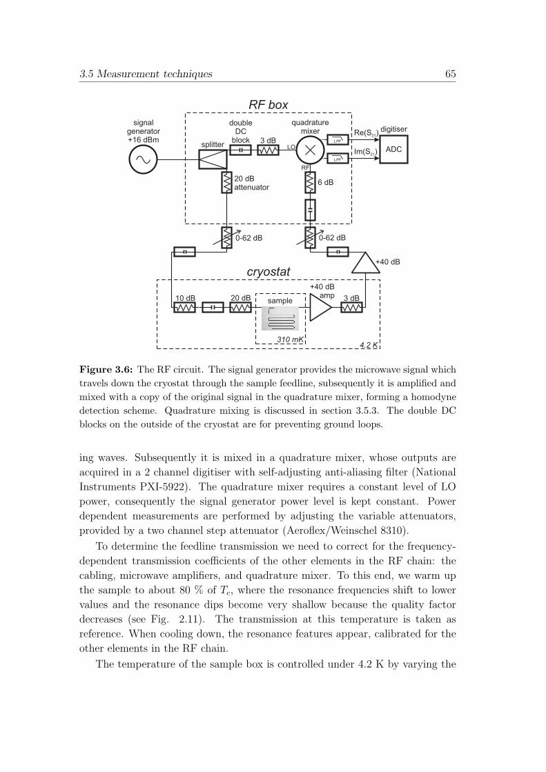
3.5 Measurement techniques 65
LPF
LPF
6 dB
3 dB
20 dBattenuator
splitter
doubleDC
block
+40 dBamp10 dB 20 dB 3 dB
quadraturemixer
signalgenerator+16 dBm
0-62 dB0-62 dB
+40 dB
Re(S )21
Im(S )21
sample
cryostat
RF box
LO
RF
ADC
digitiser
4.2 K310 mK
Figure 3.6: The RF circuit. The signal generator provides the microwave signal whichtravels down the cryostat through the sample feedline, subsequently it is amplified andmixed with a copy of the original signal in the quadrature mixer, forming a homodynedetection scheme. Quadrature mixing is discussed in section 3.5.3. The double DCblocks on the outside of the cryostat are for preventing ground loops.
ing waves. Subsequently it is mixed in a quadrature mixer, whose outputs are
acquired in a 2 channel digitiser with self-adjusting anti-aliasing filter (National
Instruments PXI-5922). The quadrature mixer requires a constant level of LO
power, consequently the signal generator power level is kept constant. Power
dependent measurements are performed by adjusting the variable attenuators,
provided by a two channel step attenuator (Aeroflex/Weinschel 8310).
To determine the feedline transmission we need to correct for the frequency-
dependent transmission coefficients of the other elements in the RF chain: the
cabling, microwave amplifiers, and quadrature mixer. To this end, we warm up
the sample to about 80 % of Tc, where the resonance frequencies shift to lower
values and the resonance dips become very shallow because the quality factor
decreases (see Fig. 2.11). The transmission at this temperature is taken as
reference. When cooling down, the resonance features appear, calibrated for the
other elements in the RF chain.
The temperature of the sample box is controlled under 4.2 K by varying the
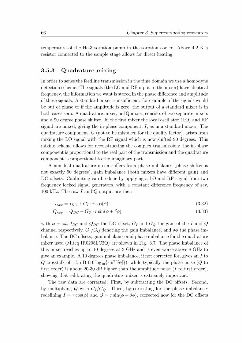
66 Chapter 3. Superconducting resonators
temperature of the He-3 sorption pump in the sorption cooler. Above 4.2 K a
resistor connected to the sample stage allows for direct heating.
3.5.3 Quadrature mixing
In order to sense the feedline transmission in the time domain we use a homodyne
detection scheme. The signals (the LO and RF input to the mixer) have identical
frequency, the information we want is stored in the phase difference and amplitude
of these signals. A standard mixer is insufficient: for example, if the signals would
be out of phase or if the amplitude is zero, the output of a standard mixer is in
both cases zero. A quadrature mixer, or IQ mixer, consists of two separate mixers
and a 90 degree phase shifter. In the first mixer the local oscillator (LO) and RF
signal are mixed, giving the in-phase component, I, as in a standard mixer. The
quadrature component, Q (not to be mistaken for the quality factor), arises from
mixing the LO signal with the RF signal which is now shifted 90 degrees. This
mixing scheme allows for reconstructing the complex transmission: the in-phase
component is proportional to the real part of the transmission and the quadrature
component is proportional to the imaginary part.
A nonideal quadrature mixer suffers from phase imbalance (phase shifter is
not exactly 90 degrees), gain imbalance (both mixers have different gain) and
DC offsets. Calibrating can be done by applying a LO and RF signal from two
frequency locked signal generators, with a constant difference frequency of say,
100 kHz. The raw I and Q output are then
Iraw = IDC + GI · r cos(φ) (3.32)
Qraw = QDC + GQ · r sin(φ + δφ) (3.33)
with φ = ωt, IDC and QDC the DC offset, GI and GQ the gain of the I and Q
channel respectively, GI/GQ denoting the gain imbalance, and δφ the phase im-
balance. The DC offsets, gain imbalance and phase imbalance for the quadrature
mixer used (Miteq IR0208LC2Q) are shown in Fig. 3.7. The phase imbalance of
this mixer reaches up to 10 degrees at 3 GHz and is even worse above 8 GHz to
give an example. A 10 degrees phase imbalance, if not corrected for, gives an I to
Q crosstalk of -15 dB (10 log10sin2[δφ]), while typically the phase noise (Q to
first order) is about 20-30 dB higher than the amplitude noise (I to first order),
showing that calibrating the quadrature mixer is extremely important.
The raw data are corrected: First, by subtracting the DC offsets. Second,
by multiplying Q with GI/GQ. Third, by correcting for the phase imbalance:
redefining I = r cos(φ) and Q = r sin(φ + δφ), corrected now for the DC offsets
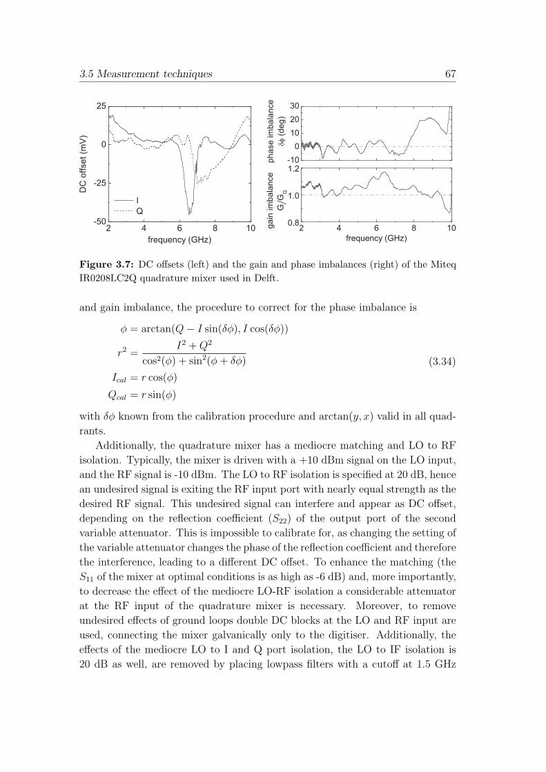
3.5 Measurement techniques 67
Figure 3.7: DC offsets (left) and the gain and phase imbalances (right) of the MiteqIR0208LC2Q quadrature mixer used in Delft.
and gain imbalance, the procedure to correct for the phase imbalance is
φ = arctan(Q− I sin(δφ), I cos(δφ))
r2 =I2 + Q2
cos2(φ) + sin2(φ + δφ)
Ical = r cos(φ)
Qcal = r sin(φ)
(3.34)
with δφ known from the calibration procedure and arctan(y, x) valid in all quad-
rants.
Additionally, the quadrature mixer has a mediocre matching and LO to RF
isolation. Typically, the mixer is driven with a +10 dBm signal on the LO input,
and the RF signal is -10 dBm. The LO to RF isolation is specified at 20 dB, hence
an undesired signal is exiting the RF input port with nearly equal strength as the
desired RF signal. This undesired signal can interfere and appear as DC offset,
depending on the reflection coefficient (S22) of the output port of the second
variable attenuator. This is impossible to calibrate for, as changing the setting of
the variable attenuator changes the phase of the reflection coefficient and therefore
the interference, leading to a different DC offset. To enhance the matching (the
S11 of the mixer at optimal conditions is as high as -6 dB) and, more importantly,
to decrease the effect of the mediocre LO-RF isolation a considerable attenuator
at the RF input of the quadrature mixer is necessary. Moreover, to remove
undesired effects of ground loops double DC blocks at the LO and RF input are
used, connecting the mixer galvanically only to the digitiser. Additionally, the
effects of the mediocre LO to I and Q port isolation, the LO to IF isolation is
20 dB as well, are removed by placing lowpass filters with a cutoff at 1.5 GHz

68 Chapter 3. Superconducting resonators
at the I and Q output. The connection from the mixer output to the digitiser
is made using a twisted pair of coaxial cables. For our case, the combination of
these steps leads to a reduction of the noise spikes to a level comparable to or
under the noise floor of the setup, i.e. effectively removing nearly all spikes in
the noise spectra.
3.5.4 Setup noise analysis
In this section the setup noise is discussed. After introducing the noise tempera-
ture, we focus on the noise for our case. Relevant expressions for the phase and
amplitude noise are given. Lastly, we find that they are in good agreement with
the data.
Noise temperature
The root mean square (RMS) voltage noise over a resistor due to thermal noise
at a temperature T is in the Rayleigh-Jeans limit (hf ¿ kT , the GHz frequencies
under consideration are far below the Planck peak) given by:
VN =√
4kTR√
B (3.35)
which corresponds to 0.9 nV/Hz1/2 at room temperature for a 50 Ω resistor; B
is the bandwidth. We now consider its Thevenin equivalent, a voltage source VN
in series with source impedance R, which is now connected to a load resistance
RL. The power dissipated in the load PL is
PL =V 2
L
RL
= V 2N
RL
(RL + R)2= 4kTB
RLR
(RL + R)2(3.36)
Maximum power transfer occurs for RL = R, and the power per unit bandwidth
dissipated in the load is
PL = kT for RL = R (3.37)
As in our RF system nearly all the components are matched to 50 Ω we can
simply express the noise power per unit bandwidth as kT .
An amplifier with gain G and input noise power PN produces an output
power Pout if an input power Pin is supplied of Pout = G · (Pin +PN) which in the
Rayleigh-Jeans limit can be rewritten as
Pout = G · (Pin + kTN) (3.38)
3.5 Measurement techniques 69
with TN the amplifier input noise temperature. The noise level kTN indicates the
noise power per unit bandwidth at the input. For an attenuator with gain G < 1
and a power Pin at its input the output power is given by:
Pout = GPin + (1−G) · kTa (3.39)
with Ta the physical temperature of the attenuator. The input noise temperature
of the attenuator is given by TN = Ta(1 − G)/G. Hence for an attenuator with
G ¿ 1, the output noise power per unit bandwidth is given by its physical
temperature.
A series combination of n elements in the chain results in a system gain of
G =∏n
j=1 Gj (cartesian) and a noise temperature of
TN = T1 +n∑
i=2
[Ti∏i−1
j=1 Gj
]= T1 +
T2
G1
+T3
G1G2
+ ... (3.40)
Our system
For our system, the RF setup is mainly noise limited by the noise sources close to
the sample: the first amplifier and the attenuator in front of the sample box. At
the input of the sample box the noise is mainly due to the physical temperature
of the last attenuator, 4.2 K, and to a lesser degree due to the 300 K thermal
radiation attenuated by 30 dB, adding 0.3 K. At the output of the sample box
the noise temperature is dominated by the low noise amplifier. We use a 4-12
GHz high electron mobility transistor amplifier (CITCRYO4-12A) [13], with an
input noise temperature of TN ≈ 3−5 K and a gain of ∼ 40 dB. Due to this high
gain, the noise temperature of the second amplifier (Miteq AFS5-00100800-14-
10P-5, TN = 110 K) hardly matters. The input noise temperature of our system
is typically TN ≈ 9K, if the gain between the sample box output and the mixer
input is kept above 60 dB, due to the noise contribution from the digitiser (see
below). This implies a readout power of under -70 dBm, as the RF input power
at the quadrature mixer lies around -10 dBm. As we use a homodyne detection
scheme, mixing two signals of the exact same frequency, the frequency noise of
the signal generator is essentially negated. Only at frequencies above several 100
MHz in the noise spectrum, well above the range we are interested in (1 Hz - 100
kHz) signal generator frequency noise can appear due to the RF cabling length.
After amplification the signal is mixed and subsequently digitised. An n-
bit digitiser has quantisation noise, yielding a signal to noise ratio of SNR =
20 log10(2n), i.e. ∼ 6.0n in dB, resulting in 144 dB for a 24 bit and 96 dB for a 16
bit digitiser. For our 24 bit digitiser (National Instruments PXI-5922) the noise
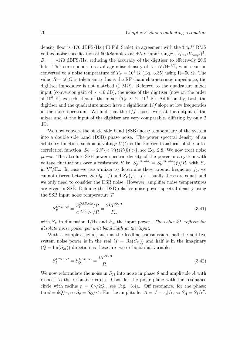
70 Chapter 3. Superconducting resonators
density floor is -170 dBFS/Hz (dB Full Scale), in agreement with the 3.4µV RMS
voltage noise specification at 50 kSample/s at ±5 V input range: (Vrms/Vrange)2 ·
B−1 = -170 dBFS/Hz, reducing the accuracy of the digitiser to effectively 20.5
bits. This corresponds to a voltage noise density of 15 nV/Hz1/2, which can be
converted to a noise temperature of TN = 105 K (Eq. 3.35) using R=50 Ω. The
value R = 50 Ω is taken since this is the RF chain characteristic impedance, the
digitiser impedance is not matched (1 MΩ). Referred to the quadrature mixer
input (conversion gain of ∼ -10 dB), the noise of the digitiser (now on the order
of 106 K) exceeds that of the mixer (TN ∼ 2 · 103 K). Additionally, both the
digitiser and the quadrature mixer have a significant 1/f slope at low frequencies
in the noise spectrum. We find that the 1/f noise levels at the output of the
mixer and at the input of the digitiser are very comparable, differing by only 2
dB.
We now convert the single side band (SSB) noise temperature of the system
into a double side band (DSB) phase noise. The power spectral density of an
arbitrary function, such as a voltage V (t) is the Fourier transform of the auto-
correlation function, SV = 2F< V (t)V (0) >, see Eq. 2.8. We now treat noise
power. The absolute SSB power spectral density of the power in a system with
voltage fluctuations over a resistance R is: SSSB,absP = SSSB,abs
V (f)/R, with SV
in V2/Hz. In case we use a mixer to determine these around frequency f0, we
cannot discern between SV (f0 + f) and SV (f0− f). Usually these are equal, and
we only need to consider the DSB noise. However, amplifier noise temperatures
are given in SSB. Defining the DSB relative noise power spectral density using
the SSB input noise temperature T
SDSB,relP =
SDSB,absV /R
< V 2 > /R=
2kT SSB
Pin
(3.41)
with SP in dimension 1/Hz and Pin the input power. The value kT reflects the
absolute noise power per unit bandwidth at the input.
With a complex signal, such as the feedline transmission, half the additive
system noise power is in the real (I = Re(S21)) and half is in the imaginary
(Q = Im(S21)) direction as these are two orthonormal variables,
SDSB,relI = SDSB,rel
Q =kT SSB
Pin
(3.42)
We now reformulate the noise in S21 into noise in phase θ and amplitude A with
respect to the resonance circle. Consider the polar plane with the resonance
circle with radius r = Ql/2Qc, see Fig. 3.4a. Off resonance, for the phase:
tan θ = δQ/r, so Sθ = SQ/r2. For the amplitude: A = |I − xc|/r, so SA = SI/r2.
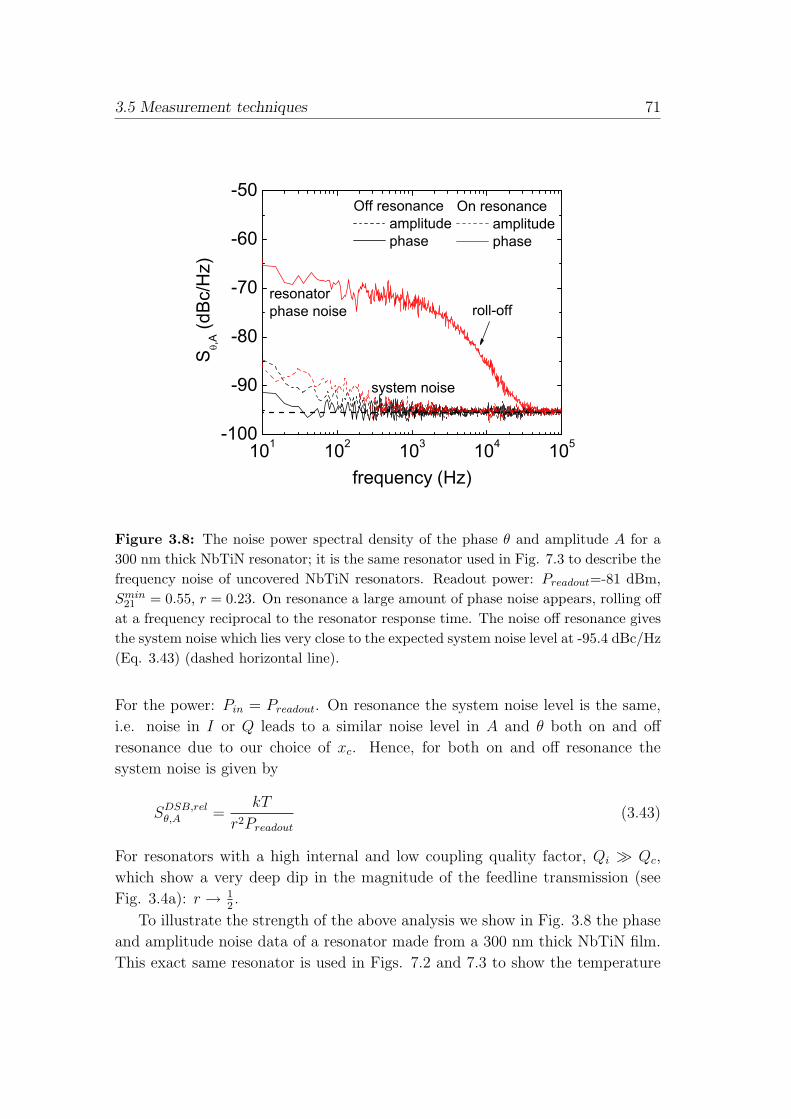
3.5 Measurement techniques 71
101 102 103 104 105-100
-90
-80
-70
-60
-50
S,A
(dB
c/H
z)
frequency (Hz)
On resonance amplitude phase
system noise
resonatorphase noise
Off resonance amplitude phase
roll-off
Figure 3.8: The noise power spectral density of the phase θ and amplitude A for a300 nm thick NbTiN resonator; it is the same resonator used in Fig. 7.3 to describe thefrequency noise of uncovered NbTiN resonators. Readout power: Preadout=-81 dBm,Smin
21 = 0.55, r = 0.23. On resonance a large amount of phase noise appears, rolling offat a frequency reciprocal to the resonator response time. The noise off resonance givesthe system noise which lies very close to the expected system noise level at -95.4 dBc/Hz(Eq. 3.43) (dashed horizontal line).
For the power: Pin = Preadout. On resonance the system noise level is the same,
i.e. noise in I or Q leads to a similar noise level in A and θ both on and off
resonance due to our choice of xc. Hence, for both on and off resonance the
system noise is given by
SDSB,relθ,A =
kT
r2Preadout
(3.43)
For resonators with a high internal and low coupling quality factor, Qi À Qc,
which show a very deep dip in the magnitude of the feedline transmission (see
Fig. 3.4a): r → 12.
To illustrate the strength of the above analysis we show in Fig. 3.8 the phase
and amplitude noise data of a resonator made from a 300 nm thick NbTiN film.
This exact same resonator is used in Figs. 7.2 and 7.3 to show the temperature
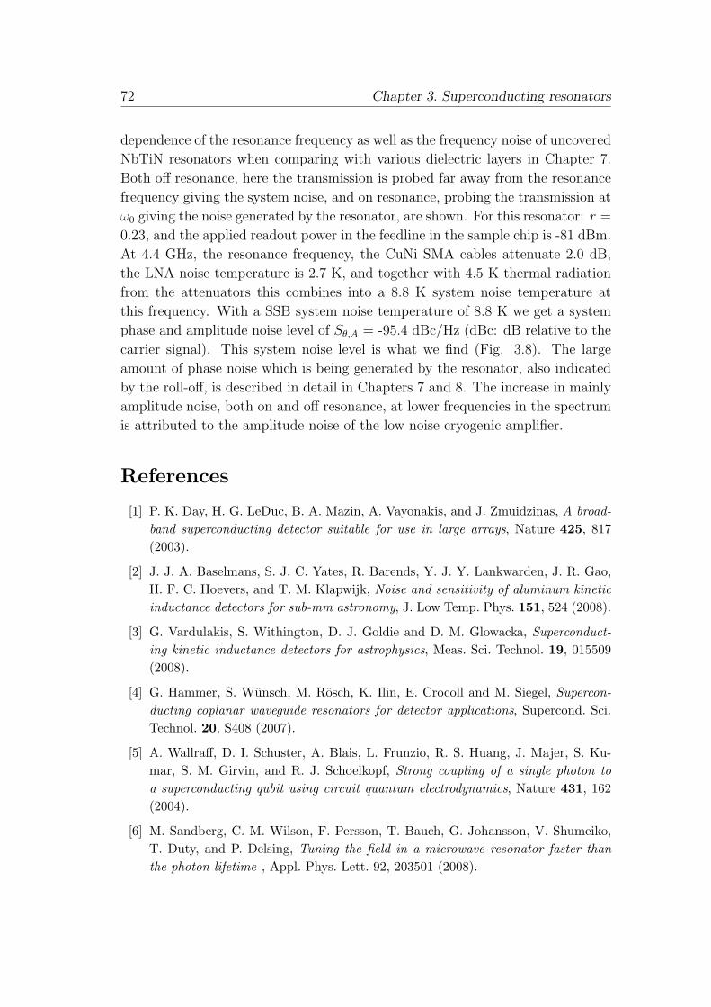
72 Chapter 3. Superconducting resonators
dependence of the resonance frequency as well as the frequency noise of uncovered
NbTiN resonators when comparing with various dielectric layers in Chapter 7.
Both off resonance, here the transmission is probed far away from the resonance
frequency giving the system noise, and on resonance, probing the transmission at
ω0 giving the noise generated by the resonator, are shown. For this resonator: r =
0.23, and the applied readout power in the feedline in the sample chip is -81 dBm.
At 4.4 GHz, the resonance frequency, the CuNi SMA cables attenuate 2.0 dB,
the LNA noise temperature is 2.7 K, and together with 4.5 K thermal radiation
from the attenuators this combines into a 8.8 K system noise temperature at
this frequency. With a SSB system noise temperature of 8.8 K we get a system
phase and amplitude noise level of Sθ,A = -95.4 dBc/Hz (dBc: dB relative to the
carrier signal). This system noise level is what we find (Fig. 3.8). The large
amount of phase noise which is being generated by the resonator, also indicated
by the roll-off, is described in detail in Chapters 7 and 8. The increase in mainly
amplitude noise, both on and off resonance, at lower frequencies in the spectrum
is attributed to the amplitude noise of the low noise cryogenic amplifier.
References
[1] P. K. Day, H. G. LeDuc, B. A. Mazin, A. Vayonakis, and J. Zmuidzinas, A broad-band superconducting detector suitable for use in large arrays, Nature 425, 817(2003).
[2] J. J. A. Baselmans, S. J. C. Yates, R. Barends, Y. J. Y. Lankwarden, J. R. Gao,H. F. C. Hoevers, and T. M. Klapwijk, Noise and sensitivity of aluminum kineticinductance detectors for sub-mm astronomy, J. Low Temp. Phys. 151, 524 (2008).
[3] G. Vardulakis, S. Withington, D. J. Goldie and D. M. Glowacka, Superconduct-ing kinetic inductance detectors for astrophysics, Meas. Sci. Technol. 19, 015509(2008).
[4] G. Hammer, S. Wunsch, M. Rosch, K. Ilin, E. Crocoll and M. Siegel, Supercon-ducting coplanar waveguide resonators for detector applications, Supercond. Sci.Technol. 20, S408 (2007).
[5] A. Wallraff, D. I. Schuster, A. Blais, L. Frunzio, R. S. Huang, J. Majer, S. Ku-mar, S. M. Girvin, and R. J. Schoelkopf, Strong coupling of a single photon toa superconducting qubit using circuit quantum electrodynamics, Nature 431, 162(2004).
[6] M. Sandberg, C. M. Wilson, F. Persson, T. Bauch, G. Johansson, V. Shumeiko,T. Duty, and P. Delsing, Tuning the field in a microwave resonator faster thanthe photon lifetime , Appl. Phys. Lett. 92, 203501 (2008).
References 73
[7] G. J. Grabovskij, L. J. Swenson, O. Buisson, C. Hoffmann, A. Monfardini, and J.C. Villegier, In situ measurement of the permittivity of helium using microwaveNbN resonators, Appl. Phys. Lett. 93, 134102 (2008).
[8] C. A. Regal, J. D. Teufel, and K. W. Lehnert, Measuring nanomechanical motionwith a microwave cavity interferometer, Nature Physics 4, 555 (2008).
[9] M. A. Castellanos-Beltran and K. W. Lehnert, Widely tunable parametric amplifierbased on a superconducting quantum interference device array resonator, Appl.Phys. Lett. 91, 083509 (2007).
[10] K. W. Lehnert, K. D. Irwin, M. A. Castellanos-Beltran, J. A. B. Mates, and L.R. Vale, Evaluation of a microwave SQUID multiplexer prototype, IEEE Trans.Appl. Sup. 17, 705 (2007).
[11] S. Doyle, P. Mauskopf, J. Naylon, A. Porch, and C. Duncombe, Lumped ele-ment kinetic inductance detectors, J. Low Temp. Phys. 151, 530 (2008); S. Doyle,Lumped element kinetic inductance detectors, Ph. D. Thesis, Cardiff University(2008).
[12] B. A. Mazin, Microwave kinetic inductance detectors, Ph. D. Thesis, CaliforniaInstitute of Technology (2004).
[13] N. Wadefalk et al., Cryogenic wide-band ultra-low-noise IF amplifiers operating atultra-low DC power, IEEE Trans. on Micr. Theory and Tech. 51, 1705 (2003).
[14] R. E. Collin, Foundations for Microwave Engineering, (McGraw-Hill, New York,1992).
[15] R. N. Simons, Coplanar waveguide circuits, components and systems, (John Wileyand Sons, 2001).
[16] J. C. Booth and C. L. Holloway, Conductor loss in superconducting planar struc-tures: Calculations and measurements, IEEE Trans. on Micr. Theory and Tech.47, 769 (1999); C. L. Holloway and E. F. Kuester, A quasi-closed form expressionfor the conductor loss of CPW lines, with an investigation of edge shape effects,IEEE Trans. on Micr. Theory and Tech. 43, 2695 (1995).
[17] J. Gao, J. Zmuidzinas, B. A. Mazin, P. K. Day, and H. G. Leduc, Experimentalstudy of the kinetic inductance fraction of superconducting coplanar waveguide,Nucl. Instr. and Meth. in Phys. Res. A 559, 585 (2006).
[18] D. M. Pozar, Microwave Engineering, Second Edition, (John Wiley and Sons,1998).
[19] D. L. Griscom, Defect structure of glasses - some outstanding questions in regardto vitreous silica, J. Non-Crystalline Solids 73, 51 (1985).
[20] R. H. Koch, D. P. DiVincenzo, and J. Clarke, Model for 1/f flux noise in SQUIDsand qubits, Phys. Rev. Lett. 98, 267003 (2007).
74 Chapter 3. Superconducting resonators
[21] B. Golding, M. von Schickfus, S. Hunklinger, and K. Dransfeld, Intrinsic electric-dipole moment of tunnelling systems in silica glasses, Phys. Rev. Lett. 43, 1817(1979).
[22] R. de Sousa, Dangling-bond spin relaxation and magnetic 1/f noise from theamorphous-semiconductor/oxide interface: Theory, Phys. Rev. B 76, 245306 (2007).
[23] B. D. Jackson, G. de Lange, T. Zijlstra, M. Kroug, J. W. Kooi, J. A. Stern, andT. M. Klapwijk, Low-noise 0.8-0.96-and 0.96-1.12-THz superconductor-insulator-superconductor mixers for the Herschel space observatory, IEEE Trans. on Micr.Theory and Tech. 54, 547 (2006).
[24] D. W. Face and D. E. Prober, Nucleation of body-centered-cubic tantalum filmswith a thin niobium underlayer, J. Vac. Sci. Tech. A 5, 3408 (1987).
[25] L. Duband, L. Clerc, and A. Ravex, Socool: A 300 K - 0.3 K pulse tube/sorptioncooler, Proc. AIP Conference 613, 1233 (2002).
[26] T. O. Klaassen, J. H. Blok, J. N. Hovenier, G. Jakob, D. Rosenthal, and K.J. Wildeman, Absorbing coatings and diffuse reflectors for the Herschel platformsub-millimeter spectrometers HIFI and PACS, Proceedings of the IEEE tenth In-ternational Conference on Terahertz Electronics, p. 32 (2002).
[27] J. J. A. Baselmans and S. J. C. Yates, private communication.
[28] On the basis of the attenuation at GHz frequencies, the attenuation at 300 GHz isexpected to be on the order of 20 dB [18] for the transverse electromagnetic (TEM)mode in a 15 cm long CuNi SMA cable with 0.86 mm outer diameter. When thewavelength is on the order of the diameter of the coaxial cable, propagation modesother than the TEM mode can be excited [18]. Some of these modes have a muchweaker attenuation, reminiscent of light in an optical fibre.
Chapter 4
Niobium and tantalum high-Q
resonators for photon detectors
We have measured the quality factors and phase noise of niobium and tanta-
lum coplanar waveguide microwave resonators on silicon. The results of both
materials are similar. We reach quality factors up to 105. At low temperatures
the quality factors show an anomalous increase, while the resonance frequency
remains constant for increasing power levels. The resonance frequency starts to
decrease at temperatures around a tenth of the critical temperature. The phase
noise exhibits a 1/f like slope. We attribute this behavior to the silicon dielectric.
This chapter is published as R. Barends, J. J. A. Baselmans, J. N. Hovenier, J. R. Gao,S. J. C. Yates, T. M. Klapwijk, and H. F. C. Hoevers, IEEE Trans. on Appl. Supercond. 17,263 (2007).
75

76 Chapter 4. Niobium and tantalum high-Q resonators for photon detectors
4.1 Introduction
One of the greatest challenges for far infrared astronomy is the development of
sensitive cameras with many pixels (100 x 100 pixels or more), having a back-
ground limited sensitivity. To date no such detector exists. Recently a new
detector concept has been proposed [1], based on kinetic inductance detectors
(KIDs).
Low Tc microwave superconducting resonators with a high quality factor and
low noise are the building blocks for KIDs. These consist of 14λ superconducting
thin film resonators with a high quality factor (Q factor). These resonators are
all capacitively coupled to a through line. Near the resonance frequency they
act as a short, and manifest themselves as a dip in the magnitude and a shift
in the phase of the through line transmission. KIDs are pair breaking detectors;
incident radiation breaks Cooper pairs into quasiparticles, changing the kinetic
inductance of the superconductor, and thus the resonance frequency [2, 3].
Typical resonance frequencies lie within the GHz band. Many resonators,
each of them having a slightly different resonance frequency, can be operated
simultaneously. With only one wideband cryogenic amplifier and commercially
available readout electronics a camera with 105 pixels can become a reality. KIDs
can address the spectrum from the submm range to X-ray, depending on the
antenna or absorber.
Recently, there is further interest in low Tc microwave superconducting res-
onators for the field of cavity quantum electrodynamics (CQED) [5]. Both in the
KIDs and CQED case low Tc resonators are operated at subkelvin temperatures.
Whether these KIDs can truly reach a background limited sensitivity is an
open question. The sensitivity is a function of the phase noise, quasiparticle
lifetime and resonator Q factor [4]. Therefore a clear understanding and charac-
terization of the device is urgently needed.
Here, we focus on the quality factor, resonance frequency and phase noise of
low Tc superconducting microwave resonators at subkelvin temperatures.
4.2 Experiment
A layout of the structure can be seen in Fig. 4.1. The chip is placed inside
a copper sample box with two SMA panel connectors, which are connected via
SMA to CPW circuit boards to the through line. The resonator is capacitively
coupled via its open end to the through line. Near the resonance frequency it acts
as a short, and a dip in the magnitude and a shift in the phase of the through
line transmission can be seen. The transmission near the resonance frequency is

4.2 Experiment 77
CPW Resonator
Coupler
Shorted end
Nb
Substrate
400 µm
1
2
Through line
Figure 4.1: The resonator layout. The light areas indicate the superconducting filmand the dark areas the substrate. The transmission line is a coplanar waveguide, thecentral line of the resonator is 3 µm wide, and the gaps are 2 µm wide. The open endof the resonator is coupled to the main through line, which runs across the chip. Theresonator is meandered due to its long length (typically a few mm).
given by
S21 =Smin
21 + i2Q δω0
ω0
1 + i2Q δω0
ω0
(4.1)
with Smin21 the size of the resonance dip, Q the loaded quality factor and ω0 the
resonance frequency. The unloaded quality factor can be extracted from the
transmission since Q−1 = Q−1c + Q−1
i and Smin21 = Qc/(Qc + Qi), with Qc the
coupling quality factor and Qi the unloaded quality factor.
The optimal materials for KIDs are still a subject of research, as low losses,
a long quasiparticle lifetime, the cryogenic system to be used and KID-antenna
coupling schemes are aspects to be considered. As superconductors niobium, due
to its relatively large gap and availability, and tantalum, for its quasiparticle
lifetime, are chosen. The niobium film is deposited using DC sputter deposition
and has a thickness of 100 nm, a critical temperature of 9.2 K and a residual
resistivity ratio (RRR) of 4. Prior to 100 nm tantalum deposition a 5 nm niobium
seed layer was sputtered to promote growth of the tantalum alpha phase [6]. The
critical temperature is 4.0 K, and the RRR is 2.5. The films are deposited on the
native oxide of a [100] oriented silicon substrate having a resistivity in excess of
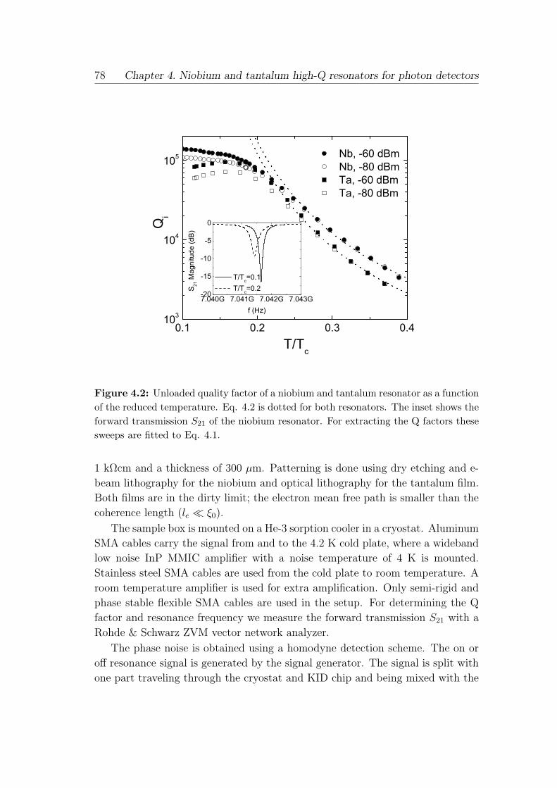
78 Chapter 4. Niobium and tantalum high-Q resonators for photon detectors
0.1 0.2 0.3 0.4103
104
105
7.040G 7.041G 7.042G 7.043G-20
-15
-10
-5
0
S 21 M
agni
tude
(dB)
f (Hz)
T/Tc=0.1 T/Tc=0.2
Qi
T/Tc
Nb, -60 dBm Nb, -80 dBm Ta, -60 dBm Ta, -80 dBm
Figure 4.2: Unloaded quality factor of a niobium and tantalum resonator as a functionof the reduced temperature. Eq. 4.2 is dotted for both resonators. The inset shows theforward transmission S21 of the niobium resonator. For extracting the Q factors thesesweeps are fitted to Eq. 4.1.
1 kΩcm and a thickness of 300 µm. Patterning is done using dry etching and e-
beam lithography for the niobium and optical lithography for the tantalum film.
Both films are in the dirty limit; the electron mean free path is smaller than the
coherence length (le ¿ ξ0).
The sample box is mounted on a He-3 sorption cooler in a cryostat. Aluminum
SMA cables carry the signal from and to the 4.2 K cold plate, where a wideband
low noise InP MMIC amplifier with a noise temperature of 4 K is mounted.
Stainless steel SMA cables are used from the cold plate to room temperature. A
room temperature amplifier is used for extra amplification. Only semi-rigid and
phase stable flexible SMA cables are used in the setup. For determining the Q
factor and resonance frequency we measure the forward transmission S21 with a
Rohde & Schwarz ZVM vector network analyzer.
The phase noise is obtained using a homodyne detection scheme. The on or
off resonance signal is generated by the signal generator. The signal is split with
one part traveling through the cryostat and KID chip and being mixed with the
4.3 Results 79
other part in an IQ mixer. The I and Q channels are sampled with a 2 channel
fast ADC card. A 2 channel variable attenuator is used to control both the
power level at the chip and the power level at the IQ mixer RF input. Hence the
magnitude and phase of the transmitted signal,√
I2 + Q2 and tan(θ) = QI, can
be monitored in time. Calculating the power spectral density gives the magnitude
and phase noise.
4.3 Results
We have measured the Q factor, frequency and phase noise of a niobium and
tantalum resonator. The niobium resonator has a resonance frequency of 7.04
GHz and a coupling quality Qc = 25 · 103. For tantalum the resonance frequency
is 2.77 GHz and Qc = 19 · 103. Both resonators have a resonance dip of around
-15 dB at base temperature. The observed behavior is similar for both devices,
therefore the results are plotted together. Typical resonance features can be seen
in the inset of Fig. 4.2, with a lowering of temperature the resonance frequency
grows and the dip deepens.
The temperature dependence of the unloaded quality factor is shown in Fig.
4.2. The quality factor rises with decreasing temperature and starts to saturate
at around T/Tc = 0.25 for both niobium and tantalum. The rise follows the two
fluid Mattis-Bardeen description of a superconductor [7],
QMB =2
α
σ2
σ1
(4.2)
with σ = σ1 − iσ2 the complex conductivity and α = Lk
Ltthe kinetic inductance
fraction. The difference between niobium and tantalum in the unloaded Q factor
is due to α.
The unloaded Q factor can be written as Q−1i = Q−1
MB + Q−1s , with Qs the
saturation Q factor, representing the deviation from Mattis-Bardeen theory. At
lower temperatures, the Mattis-Bardeen description is no longer applicable, as
the Q factor saturates at around 105 for both niobium and tantalum, a value
which is comparable to results on aluminum KIDs [4]. At T/Tc = 0.13 a small
jump upwards in the niobium Q factor can be seen and a slight decrease in the
tantalum Q factor occurs for T/Tc < 0.15. As the readout power is lowered
from -60 dBm to -80 dBm, clearly the saturation Q factor decreases, while the Q
factor in the range where the Mattis-Bardeen description is valid does not visibly
change.
The latter is shown in more detail in Fig. 4.3; the unloaded Q factor is
plotted for varying power levels and constant temperatures. Only in the satura-
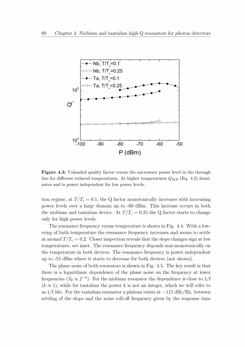
80 Chapter 4. Niobium and tantalum high-Q resonators for photon detectors
-100 -90 -80 -70 -60 -50104
105
Nb, T/Tc=0.1 Nb, T/Tc=0.25 Ta, T/Tc=0.1 Ta, T/Tc=0.25
Qi
P (dBm)
Figure 4.3: Unloaded quality factor versus the microwave power level in the throughline for different reduced temperatures. At higher temperatures QMB (Eq. 4.2) domi-nates and is power independent for low power levels.
tion regime, at T/Tc = 0.1, the Q factor monotonically increases with increasing
power levels over a large domain up to -60 dBm. This increase occurs in both
the niobium and tantalum device. At T/Tc = 0.25 the Q factor starts to change
only for high power levels.
The resonance frequency versus temperature is shown in Fig. 4.4. With a low-
ering of bath temperature the resonance frequency increases and seems to settle
at around T/Tc = 0.2. Closer inspection reveals that the slope changes sign at low
temperatures, see inset. The resonance frequency depends non-monotonically on
the temperature in both devices. The resonance frequency is power independent
up to -55 dBm where it starts to decrease for both devices (not shown).
The phase noise of both resonators is shown in Fig. 4.5. The key result is that
there is a logarithmic dependence of the phase noise on the frequency at lower
frequencies (Sθ ∝ f−k). For the niobium resonator the dependence is close to 1/f
(k ≈ 1), while for tantalum the power k is not an integer, which we will refer to
as 1/f like. For the tantalum resonator a plateau exists at −115 dBc/Hz, between
settling of the slope and the noise roll-off frequency given by the response time
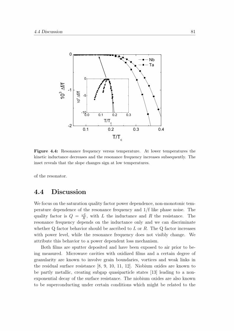
4.4 Discussion 81
0.1 0.2 0.3 0.4-2
-1
0
0.0 0.1 0.2 0.3-10
-5
0
10
6 f/f
T/Tc
Nb Ta
103
f/f
T/Tc
Figure 4.4: Resonance frequency versus temperature. At lower temperatures thekinetic inductance decreases and the resonance frequency increases subsequently. Theinset reveals that the slope changes sign at low temperatures.
of the resonator.
4.4 Discussion
We focus on the saturation quality factor power dependence, non-monotonic tem-
perature dependence of the resonance frequency and 1/f like phase noise. The
quality factor is Q = ωLR
, with L the inductance and R the resistance. The
resonance frequency depends on the inductance only and we can discriminate
whether Q factor behavior should be ascribed to L or R. The Q factor increases
with power level, while the resonance frequency does not visibly change. We
attribute this behavior to a power dependent loss mechanism.
Both films are sputter deposited and have been exposed to air prior to be-
ing measured. Microwave cavities with oxidized films and a certain degree of
granularity are known to involve grain boundaries, vortices and weak links in
the residual surface resistance [8, 9, 10, 11, 12]. Niobium oxides are known to
be partly metallic, creating subgap quasiparticle states [13] leading to a non-
exponential decay of the surface resistance. The niobium oxides are also known
to be superconducting under certain conditions which might be related to the
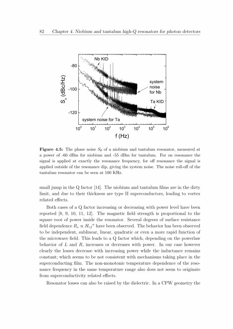
82 Chapter 4. Niobium and tantalum high-Q resonators for photon detectors
100 101 102 103 104 105 106
-120
-100
-80
system noise for Ta
Ta KID
systemnoisefor Nb
S (d
Bc/
Hz)
f (Hz)
Nb KID
Figure 4.5: The phase noise Sθ of a niobium and tantalum resonator, measured ata power of -60 dBm for niobium and -55 dBm for tantalum. For on resonance thesignal is applied at exactly the resonance frequency, for off resonance the signal isapplied outside of the resonance dip, giving the system noise. The noise roll-off of thetantalum resonator can be seen at 100 KHz.
small jump in the Q factor [14]. The niobium and tantalum films are in the dirty
limit, and due to their thickness are type II superconductors, leading to vortex
related effects.
Both cases of a Q factor increasing or decreasing with power level have been
reported [8, 9, 10, 11, 12]. The magnetic field strength is proportional to the
square root of power inside the resonator. Several degrees of surface resistance
field dependence Rs ∝ Hrfn have been observed. The behavior has been observed
to be independent, sublinear, linear, quadratic or even a more rapid function of
the microwave field. This leads to a Q factor which, depending on the powerlaw
behavior of L and R, increases or decreases with power. In our case however
clearly the losses decrease with increasing power while the inductance remains
constant; which seems to be not consistent with mechanisms taking place in the
superconducting film. The non-monotonic temperature dependence of the reso-
nance frequency in the same temperature range also does not seem to originate
from superconductivity related effects.
Resonator losses can also be raised by the dielectric. In a CPW geometry the
4.5 Conclusions 83
electric fields stand between the center and outer conductors, and are strongest at
the silicon surface. The devices are exposed to air prior to being measured, and
native oxide is formed. Native silicon oxide formed on [100] wafers is amorphous
[15].
Microwave properties of amorphous systems are known to be affected by two
level systems [16, 17]. Two level systems with a dipole moment can couple to the
electric field and the associated dielectric losses reduce with a growing microwave
field intensity. The dielectric constant and thus the resonance frequency can also
be affected. Depending on wether resonant or relaxation two level systems dom-
inate, the dielectric constant shrinks or grows with an increase of temperature.
The small decrease of the resonance frequency at low temperatures is consistent
with resonant tunneling systems in amorphous dielectrics [16]. The importance
of dipole defects has recently been appreciated in relating the decrease of losses
to the substrate in a superconducting cavity [18].
The phase noise of both resonators shows a 1/f like slope. Our measurements
are in agreement with earlier results on KIDs with aluminum CPW resonators
on silicon [4]. Moreover, in this experiment the silicon substrate was replaced
by a sapphire one or etched away, leading in both cases to a reduction in Sθ
of around 20 dBc/Hz at low frequencies, convincingly showing that a 1/f like
noise source, in their case a dominant one, resides in or on the silicon substrate.
It is interesting to note that two level systems are a possible 1/f noise source
[19, 20]. For our case the noise in the dielectric constant translates into noise in
the resonance frequency and observed phase.
4.5 Conclusions
To conclude, we have measured the quality factor, resonance frequency and phase
noise of niobium and tantalum on silicon 14λ CPW GHz resonators, with tem-
peratures down to 300 mK. The measurements were done using a vector network
analyzer and IQ mixer.
The results of the niobium and tantalum resonator are similar. In both ma-
terials the quality factor follows Mattis-Bardeen theory up to a saturation value,
typically being 105. This saturation value is comparable to results on aluminum
KIDs. The saturation Q factor increases with readout power, while the resonance
frequency starts to decrease only at high power levels. We attribute the Q factor
power dependence to a decrease of microwave losses for increasing power levels.
The resonance frequency has a non-monotonic temperature dependence. When
lowering the temperature the resonance frequency grows, yet at around a tenth
84 Chapter 4. Niobium and tantalum high-Q resonators for photon detectors
of the critical temperature the frequency starts to decrease. The phase noise of
both resonators exhibits a 1/f like slope. Superconductivity related mechanisms
are not enough to explain this behavior. The various mechanisms in the super-
conductor such as film granularity and vortices are known to increase the surface
impedance with increasing power in the low power limit, whereas we observe the
opposite.
Qualitatively the Q factor power dependence, non-monotonic frequency tem-
perature dependence and 1/f like slope in the phase noise at low temperatures
could be attributed to two level systems in the silicon dielectric. The resonators
used here are a unique tool capable of observing these probably interrelated ef-
fects. Further research is needed to understand the saturation regime and identify
the limitations of low temperature microwave resonators.
References
[1] P. K. Day, H. G. LeDuc, B. A. Mazin, A. Vayonakis and J. Zmuidzinas, A broad-band superconducting detector for use in large arrays, Nature 425, 817 (2003).
[2] S. Doyle, J. Naylon, J. Cox, P. Mauskopf, A. Porch, Kinetic inductance detectorsfor 200 µm astronomy, Proc. SPIE 6275, 6275O1 (2006).
[3] J. J. A. Baselmans, R. Barends, S. J. C. Yates, J. N. Hovenier, J. R. Gao, H.F. C. Hoevers and T. M. Klapwijk, Development of high-Q superconducting res-onators for use as kinetic inductance detectors, Proc. 7th Int. Workshop on LowTemperature Electronics, Noordwijk, The Netherlands, June 2006.
[4] B. A. Mazin, Microwave kinetic inductance detectors, Ph.D. dissertation, Califor-nia Institute of Technology, 2004.
[5] A. Wallraff, D. I. Schuster, A. Blais, L. Frunzio, R. S. Huang, J. Majer, S. Ku-mar, S. M. Girvin and R. J. Schoelkopf, Strong coupling of a single photon toa superconducting qubit using circuit quantum electrodynamics, Nature 431, 162(2004).
[6] D. W. Face and D. E. Prober, Nucleation of body-centered-cubic tantalum filmswith a thin niobium underlayer, J. Vac. Sci. Tech. A 5, 3408 (1987).
[7] D. C. Mattis and J. Bardeen, Theory of the anomalous skin effect in normal andsuperconducting metals, Phys. Rev. 111, 412 (1958).
[8] A. V. Velichko, M. J. Lancaster and A. Porch, Nonlinear microwave properties ofhigh Tc thin films, Supercond. Sci. Technol. 18, R24 (2005).
[9] J. Halbritter, Transport in superconducting niobium films for radio frequency ap-plications, J. Appl. Phys. 97, 083904 (2005).
References 85
[10] C. Attanasio, L. Maritato and R. Vaglio, Residual surface resistance of polycrys-talline superconductors, Phys. Rev. B 43, 6128 (1991).
[11] C. C. Chin, D. E. Oates, G. Dresselhaus and M. S. Dresselhaus, Nonlinear elec-trodynamics of superconducting NbN and Nb thin films at microwave frequencies,Phys. Rev. B 45, 4788 (1992).
[12] P. Lahl and R. Wordenweber, Fundamental microwave-power-limiting mechanismof epitaxial high-temperature superconducting thin-film devices, J. Appl. Phys 97,113911 (2005).
[13] M. Ohkubo, J. Martin, K. Drachsler, R. Gross, R. P. Huebener, I. Sakamotoand N. Hyashi, Asymmetric response of superconducting niobium-tunnel-junctionx-ray detectors, Phys. Rev. B 54, 9484 (1996).
[14] J. K. Hulm, C. K. Jones, R. A. Hein and J. W. Gibson, Superconductivity in theTiO and NbO systems, J. Low Temp. Phys. 7, 291 (1972).
[15] A. H. Carim, M. M. Dovek, C. F. Quate, R. Sinclair and C. Vorst, High-resolutionelectron microscopy and scanning tunneling microscopy of native oxides on silicon,Science 237, 630 (1987).
[16] C. Enss and S. Hunklinger, Low-Temperature Physics, (Springer Verlag, 2005).
[17] W. A. Phillips, Two-level states in glasses, Rep. Prog. Phys. 50, 1657 (1987).
[18] M. A. Hein, D. E. Oates, P. J. Hirst, R. G. Humphreys and A. V. Velichko,Nonlinear dielectric microwave losses in MgO substrates, Appl. Phys. Lett. 80,1007 (2002).
[19] M. B. Weissman, 1/f noise and other slow, nonexponential kinetics in condensedmatter, Rev. Mod. Phys. 60, 537 (1988).
[20] C. C. Yu, Why study noise due to two level systems: a suggestion for experimen-talists, J. Low Temp. Phys. 137, 251 (2004).
86 Chapter 4. Niobium and tantalum high-Q resonators for photon detectors

Chapter 5
Quasiparticle relaxation in
optically excited high-Q
superconducting resonators
The quasiparticle relaxation time in superconducting films has been measured as a
function of temperature using the response of the complex conductivity to photon
flux. For tantalum and aluminium, chosen for their difference in electron-phonon
coupling strength, we find that at high temperatures the relaxation time increases
with decreasing temperature, as expected for electron-phonon interaction. At
low temperatures we find in both superconducting materials a saturation of the
relaxation time, suggesting the presence of a second relaxation channel not due
to electron-phonon interaction.
This chapter is published as R. Barends, J. J. A. Baselmans, S. J. C. Yates, J. R. Gao,J. N. Hovenier, and T. M. Klapwijk, Phys. Rev. Lett. 100, 257002 (2008).
87

88 Chapter 5. Quasiparticle relaxation in high-Q superconducting resonators
5.1 Introduction
The equilibrium state of a superconductor at finite temperatures consists of the
Cooper pair condensate and thermally excited quasiparticles. The quasiparticle
density nqp decreases exponentially with decreasing temperature. These charge
carriers control the high frequency (ω) response of the superconductor through
the complex conductivity σ1 − iσ2. At nonzero frequencies the real part σ1 de-
notes the conductivity by quasiparticles and the imaginary part σ2 is due to
the superconducting condensate [1, 2]. When the superconductor is driven out of
equilibrium it relaxes back to the equilibrium state by the redistribution of quasi-
particles over energy and by recombination of quasiparticles to Cooper pairs. The
recombination is a binary reaction, quasiparticles with opposite wavevector and
spin combine, and the remaining energy is transferred to another excitation. The
latter process is usually controlled by the material dependent electron-phonon in-
teraction [3, 4]. With decreasing temperatures the recombination time increases
exponentially reflecting the reduced availability of quasiparticles. Here, we re-
port relaxation time measurements in superconducting films far below the critical
temperature Tc. We find strong deviations from exponentially rising behavior,
which we attribute to the emergence of an additional relaxation channel in the
superconducting films.
5.2 Probing quasiparticle relaxation with the
complex conductivity
We have measured the time dependence of the complex conductivity of super-
conducting films after applying an optical photon pulse. In addition, the noise
spectrum is measured in the presence of a continuous photon flux [5]. The su-
perconducting film is patterned as a planar microwave resonator. The resonator
is formed by a meandering coplanar waveguide (CPW), with the central line 3
µm and the slits 2 µm wide, and is coupled to a feedline, see Fig. 5.1a [6].
The complex conductivity results in a kinetic inductance Lk ∝ 1/dωσ2, for thin
films with thickness d, which is due to the inertia of the Cooper pair conden-
sate. It sets together with the length of the central line the resonance frequency:
ω0 = 2π/4l√
(Lg + Lk)C, with l the length of a quarterwave resonator, Lg the
geometric inductance and C the capacitance, both per unit length. The variation
in kinetic inductance due to photons is connected to the quasiparticle density nqp
by δLk/Lk = 12δnqp/ncp, with ncp the Cooper pair density (nqp ¿ ncp). Res-
onance frequencies used lie between 3-6 GHz. For a quarterwave resonator at

5.2 Probing quasiparticle relaxation with the complex conductivity 89
(a) (b)
(c)
1 2
~
cryostat
Real
Imag-
inary
X
signal
generator
quadrature
mixer
LNA
Figure 5.1: (a) A quarter wavelength resonator, capacitively coupled to a feedline,formed by the superconducting film (gray) interrupted by slits (black). (b) The res-onator exhibits a dip in the magnitude and circle in the complex plane (inset) of thefeedline transmission S21. (c) The feedline transmission is converted into a phase θ andamplitude A using the equilibrium resonance circle as reference (right inset). The re-sponse to an optical pulse of length 0.5 µs (at t=0) (open circles) exhibits an initial risedue to the response time (3.7 µs) of the resonator and subsequently follows an expo-nential decay (34 µs) (dashed), reflecting the restoration of equilibrium (Eq. 5.1). Theresponse is measured with a signal generator, low noise amplifier (LNA) and quadraturemixer (upper inset).
6 GHz, the length of the meandering superconducting CPW-line is 5 mm. The
resonator is capacitively coupled by placing a part parallel to the feedline.
The resonators are made from superconducting materials with different electron-
90 Chapter 5. Quasiparticle relaxation in high-Q superconducting resonators
phonon interaction strengths, tantalum (strong interaction) and aluminium (weak
interaction). The tantalum film, 150 nm thick, is sputtered on a high resistivity
silicon substrate. A 6 nm thick niobium seed layer is used to promote the growth
of the desired tantalum alpha phase [7]. The critical temperature Tc is 4.43 K, the
low temperature resistivity ρ is 8.4 µΩcm and the residual resistance ratio (RRR)
is 3.0. A 100 nm thick aluminium film is sputtered on silicon (Tc=1.25, ρ=1.3
µΩcm, RRR=3.7). Alternatively, a film of 250 nm thick is sputtered on silicon
(Tc=1.22, ρ=1.0 µΩcm, RRR=6.9) and another one of 250 nm is sputtered on A-
plane sapphire (Tc=1.20, ρ=0.25 µΩcm, RRR=11). The samples are patterned
using optical lithography, followed by wet etching for aluminium and reactive ion
etching for tantalum. For both materials quality factors in the order of 106 are
reached. The sample is cooled in a cryostat with an adiabatic demagnetization
refrigerator. The sample space is surrounded by a cryoperm and a superconduct-
ing magnetic shield. Alternatively, the sample is cooled in a cryostat with a 3He
sorption cooler without magnetic shields. A GaAsP LED (1.9 eV) acts as photon
source, fibre-optically coupled to the sample box.
The complex transmission S21 of the circuit is measured by sweeping the
frequency of the signal applied along the feedline (Fig. 5.1a). Near the resonance
frequency ω0 the feedline transmission exhibits a decrease in magnitude and traces
a circle in the complex plane (full lines in Fig. 5.1b). A non-equilibrium state
results in a resonance frequency shift and broadening of the dip, and a reduction
and shift of the resonance circle in the complex plane (dashed lines in Fig. 5.1b).
The actual signals (filled dot and open circle in Fig. 5.1b) are obtained by
sending a continuous wave at the equilibrium resonance frequency ω0 through
the feedline, which is amplified and mixed with a copy of the original signal in a
quadrature mixer, whose output gives the real and imaginary part of the feedline
transmission (upper inset Fig. 5.1c). The non-equilibrium response (open circle),
compared to the equilibrium response (filled dot), is characterized by a changed
phase θ and amplitude A, referred to a shifted origin in the complex plane (from
the equilibrium position xc).
The phase θ with respect to the resonance circle center xc is given by θ =
arctanIm (S21)/[xc − Re (S21)] and is related to the change in resonance fre-
quency by: θ = −4Q δω0
ω0, with Q the resonator loaded quality factor [6]. A related
change in Lk is given by δω0/ω0 = −α2δLk/Lk, with α the ratio of the kinetic to
the total inductance. The phase θ is therefore a direct measure of the change in
complex conductivity (given in the dirty limit by):
θ = −2αQδσ2
σ2
(f(E), ∆
), (5.1)
with f(E) the electronic distribution function characterizing the non-equilibrium

5.3 Relaxation in the frequency domain 91
and ∆ the superconductor energy gap.
The amplitude A depends predominantly on σ1 and to a smaller degree on
σ2. The amplitude is determined by the complex transmission S21 by: A =√[Re(S21)− xc]2 + Im(S21)2/(1 − xc). On resonance S21 = Qc/(Qc + Qu) with
Qu ∝ σ2/σ1 the unloaded resonator quality factor and Qc the coupling quality
factor, leading to
A = 1− 2Q
Qu
[δσ1
σ1
(f(E), ∆
)− δσ2
σ2
(f(E), ∆
)]. (5.2)
By measuring A and θ in the frequency- and time-domain we obtain direct infor-
mation on the relaxation through the complex conductivity of the superconduct-
ing films.
5.3 Relaxation in the frequency domain
A typical pulse response is shown in Fig. 5.1c. The initial rise of the phase θ is
due to the response time of the resonator. The relaxation shows up as an expo-
nential decay. The right inset of Fig. 5.1c shows the evolution of the response
in the transformed polar plane. These data are interpreted as governed by one
relaxation time. This is justified by performing measurements of the noise spec-
trum and applying the analysis by Wilson et al. [5]. Since the superconducting
condensate and the quasiparticle excitations form a two-level system a Lorentzian
spectrum is expected, with the relaxation time determining the roll-off frequency.
If more dominant relaxation processes are present, the noise spectrum is no longer
a single Lorentzian [8]. We have studied the superconducting films under expo-
sure to a continuous photon flux. Our films are exposed to an optical white noise
signal due to photon shot noise, resulting in fluctuations in f(E). Where a single
time τ determines the relaxation process the phase or amplitude noise spectrum
is
Sθ,A =2~ΩP
rθ,A
1 + (2πfτ)2, (5.3)
with P the absorbed power, ~Ω the photon energy, and rθ,A denoting the respon-
sivity of the phase or amplitude to an optical signal.
The measured noise power spectra of the amplitude and phase of a tantalum
sample are shown in Fig. 5.2. In equilibrium the amplitude noise spectrum is
flat over the full range, and the phase noise follows 1/fa with a ≈ 0.25. The
amplitude noise is due to the amplifier, remaining unchanged at frequencies far
away from ω0 while the phase noise is dominated by resonator noise [9, 10], rolling
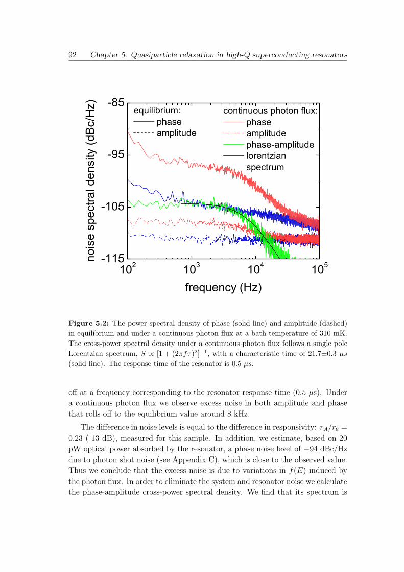
92 Chapter 5. Quasiparticle relaxation in high-Q superconducting resonators
102 103 104 105-115
-105
-95
-85
no
ise
spec
tral d
ensi
ty (d
Bc/
Hz)
frequency (Hz)
equilibrium: phase amplitude
continuous photon flux: phase amplitude phase-amplitude lorentzian
spectrum
Figure 5.2: The power spectral density of phase (solid line) and amplitude (dashed)in equilibrium and under a continuous photon flux at a bath temperature of 310 mK.The cross-power spectral density under a continuous photon flux follows a single poleLorentzian spectrum, S ∝ [1 + (2πfτ)2]−1, with a characteristic time of 21.7±0.3 µs
(solid line). The response time of the resonator is 0.5 µs.
off at a frequency corresponding to the resonator response time (0.5 µs). Under
a continuous photon flux we observe excess noise in both amplitude and phase
that rolls off to the equilibrium value around 8 kHz.
The difference in noise levels is equal to the difference in responsivity: rA/rθ =
0.23 (-13 dB), measured for this sample. In addition, we estimate, based on 20
pW optical power absorbed by the resonator, a phase noise level of −94 dBc/Hz
due to photon shot noise (see Appendix C), which is close to the observed value.
Thus we conclude that the excess noise is due to variations in f(E) induced by
the photon flux. In order to eliminate the system and resonator noise we calculate
the phase-amplitude cross-power spectral density. We find that its spectrum is
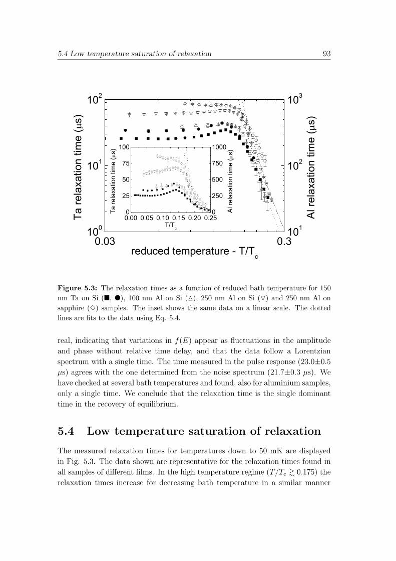
5.4 Low temperature saturation of relaxation 93
0.03 0.3100
101
102
101
102
103
Ta re
laxa
tion
time
(s)
reduced temperature - T/Tc
0.00 0.05 0.10 0.15 0.20 0.250
25
50
75
100
0
250
500
750
1000
Ta re
laxa
tion
time
(s)
T/TcA
l rel
axat
ion
time
(s)
Al r
elax
atio
n tim
e (
s)
Figure 5.3: The relaxation times as a function of reduced bath temperature for 150nm Ta on Si (¥, l), 100 nm Al on Si (M), 250 nm Al on Si (O) and 250 nm Al onsapphire (3) samples. The inset shows the same data on a linear scale. The dottedlines are fits to the data using Eq. 5.4.
real, indicating that variations in f(E) appear as fluctuations in the amplitude
and phase without relative time delay, and that the data follow a Lorentzian
spectrum with a single time. The time measured in the pulse response (23.0±0.5
µs) agrees with the one determined from the noise spectrum (21.7±0.3 µs). We
have checked at several bath temperatures and found, also for aluminium samples,
only a single time. We conclude that the relaxation time is the single dominant
time in the recovery of equilibrium.
5.4 Low temperature saturation of relaxation
The measured relaxation times for temperatures down to 50 mK are displayed
in Fig. 5.3. The data shown are representative for the relaxation times found in
all samples of different films. In the high temperature regime (T/Tc & 0.175) the
relaxation times increase for decreasing bath temperature in a similar manner
94 Chapter 5. Quasiparticle relaxation in high-Q superconducting resonators
for both tantalum and aluminium samples until a new regime is entered around
T/Tc ∼ 0.15. The tantalum samples clearly show a non-monotonic temperature
dependence, exhibiting a maximum near T/Tc ∼ 0.15. Two aluminium films
show a less pronounced non-monotonic temperature dependence. We do not
see a non-monotonic temperature dependence in samples of aluminium with the
lowest level of disorder (highest RRR). Below T/Tc ∼ 0.1 the relaxation times
become temperature independent at a plateau value of 25-35 µs for Ta, 390 µs
for 100 nm thick Al on Si, 600 µs for 250 nm thick Al on Si and 860 µs for 250
nm thick Al on sapphire.
The relaxation times for aluminium are measured in half wavelength res-
onators where the central line is isolated from the ground plane. For the directly
connected quarter wavelength resonators a length dependence was found. For
tantalum the values are found to be length independent in both cases. Conse-
quently, the data shown are not influenced by quasiparticle outdiffusion. Also, the
relaxation times remain unchanged when instead of an optical pulse a microwave
pulse at frequency ω0 is used. In this method only quasiparticle excitations near
the gap energy are created by the pair-breaking current. This observation leads
us to believe that the observed decay is due to recombination of quasiparticles
with energies near the gap.
The exponential temperature dependence for T/Tc & 0.175 is consistent with
the theory of recombination by electron-phonon interaction [4]. The dotted lines
in Fig. 5.3 follow the expression for the recombination time,
1
τrec
=1
τ0
√π( 2∆
kTc
)5/2√
T
Tc
e−∆kT , (5.4)
with τ0 a material-specific electron-phonon scattering time. We find for 150 nm
Ta on Si τ0 = 42±2 ns and for 250 nm Al on Si τ0 = 687±6 ns. The deviation from
the exponential rise and the low temperature behavior is incompatible with the
established theory for electron-phonon relaxation. We assume that an additional
relaxation channel [11] is dominant at low temperatures, where the electron-
phonon mechanism becomes too slow.
5.5 Discussion
In previous experiments using superconducting tunnel junctions a similar satu-
ration in the quasiparticle loss has been reported. For photon detectors inverse
loss rates in the order of tens of microseconds have been found for tantalum
[12, 13, 14, 15] and hundreds of microseconds for aluminium [6]. Some of these
experiments also indicated a non-monotonic temperature dependence [16]. Most

References 95
of these observations have been attributed to trapping states at surfaces or in
dielectrics. The fact that our similar experimental results occur in simple su-
perconducting films and two different materials suggests that processes in the
superconducting film itself lead to the observed low temperature behavior.
The observed saturation in the relaxation times in our samples is reminiscent
of experiments in normal metals on inelastic scattering in non-thermal distribu-
tions and on dephasing in weak localization studies. The apparent saturation
of the dephasing time and the strong quasiparticle energy exchange at low tem-
peratures have been shown to be caused by dilute concentrations of magnetic
impurities [17, 18, 19, 20]. It is known that in superconductors a large density
of magnetic impurities decreases the critical temperature. For dilute magnetic
impurities the local properties are most important. In experiments with mag-
netic adatoms impurity bound excitations arise [21], tails in the density of states
within the gap might form and the formation of an intragap band with growing
impurity concentration are predicted [22, 23]. In ongoing experiments we observe
a gradual decrease of the relaxation time with an increasing ion-implanted mag-
netic impurity concentration (0-100 ppm). However, disorder plays a role as well
and further experiments are needed to clarify possible relaxation processes [24].
In conclusion, we find that the quasiparticle relaxation times, probed by means
of the complex conductivity, saturate for both tantalum and aluminium, below a
tenth of the critical temperature. We suggest that the saturation of the relaxation
time is due to the presence of a relaxation channel, which is not caused by the
conventional process dominated by electron-phonon interaction.
References
[1] M. Tinkham, Introduction to Superconductivity (McGraw-Hill, New York, 1996).
[2] D. C. Mattis and J. Bardeen, Theory of the anomalous skin effect in normal andsuperconducting metals, Phys. Rev. 111, 412 (1958).
[3] B. I. Miller and A. H. Dayem, Relaxation and recombination times of quasiparticlesin superconducting Al thin films, Phys. Rev. Lett. 18, 1000 (1967).
[4] S. B. Kaplan, C. C. Chi, D. N. Langenberg, J. J. Chang, S. Jafarey, and D. J.Scalapino, Quasiparticle and phonon lifetimes in superconductors, Phys. Rev. B14, 4854 (1976).
[5] C. M. Wilson, L. Frunzio, and D. E. Prober, Time-resolved measurements ofthermodynamic fluctuations of the particle number in a nondegenerate Fermi gas,Phys. Rev. Lett. 87, 067004 (2001).
96 Chapter 5. Quasiparticle relaxation in high-Q superconducting resonators
[6] P. K. Day, H. G. LeDuc, B. A. Mazin, A. Vayonakis, and J. Zmuidzinas, A broad-band superconducting detector suitable for use in large arrays, Nature 425, 817(2003).
[7] D. W. Face and D. E. Prober, Nucleation of body-centered-cubic tantalum filmswith a thin niobium underlayer, J. Vac. Sci. Tech. A 5, 3408 (1987).
[8] C. M. Wilson and D. E. Prober, Quasiparticle number fluctuations in supercon-ductors, Phys. Rev. B 69, 094524 (2004).
[9] J. Gao, J. Zmuidzinas, B. A. Mazin, H. G. LeDuc, and P. K. Day, Noise propertiesof superconducting coplanar waveguide microwave resonators, Appl. Phys. Lett.90, 102507 (2007).
[10] R. Barends, H. L. Hortensius, T. Zijlstra, J. J. A. Baselmans, S. J. C. Yates, J.R. Gao, and T. M. Klapwijk, Contribution of dielectrics to frequency and noise ofNbTiN superconducting resonators, Appl. Phys. Lett. 92, 223502 (2008).
[11] A possible contribution to quasiparticle recombination by electron-electron inter-action involving a three body process has been proposed in M. Reizer, Electron-electron relaxation in two-dimensional impure superconductors, Phys. Rev. B 61,7108 (2000); in which also an exponential increase with decreasing temperature ispredicted.
[12] P. Verhoeve, R. den Hartog, A. G. Kozorezov, D. Martin, A. van Dordrecht, J. K.Wigmore, and A. Peacock, Time dependence of tunnel statistics and the energyresolution of superconducting tunnel junctions, J. Appl. Phys. 92, 6072 (2002).
[13] T. Nussbaumer, Ph. Lerch, E. Kirk, A. Zehnder, R. Fuchslin, P. F. Meier, andH. R. Ott, Quasiparticle diffusion in tantalum using superconducting tunnel junc-tions, Phys. Rev. B 61, 9719 (2000).
[14] L. Li, L. Frunzio, C. M. Wilson, and D. E. Prober, Quasiparticle nonequilibriumdynamics in a superconducting Ta film, J. Appl. Phys. 93, 1137 (2003).
[15] B. A. Mazin, B. Bumble, P. K. Day, M. E. Eckart, S. Golwala, J. Zmuidzinas,and F. A. Harrison, Position sensitive x-ray spectrophotometer using microwavekinetic inductance detectors, Appl. Phys. Lett., 89, 222507 (2006).
[16] A. G. Kozorezov, J. K. Wigmore, A. Peacock, A. Poelaert, P. Verhoeve, R. denHartog, and G. Brammertz, Local trap spectroscopy in superconducting tunneljunctions, Appl. Phys. Lett. 78, 3654 (2001).
[17] F. Pierre, A. B. Gougam, A. Anthore, H. Pothier, D. Esteve, and N. O. Birge,Dephasing of electrons in mesoscopic metal wires, Phys. Rev. B 68, 085413 (2003).
[18] A. Anthore, F. Pierre, H. Pothier, and D. Esteve, Magnetic-field-dependent quasi-particle energy relaxation in mesoscopic wires, Phys. Rev. Lett. 90, 076806 (2003).
References 97
[19] B. Huard, A. Anthore, N. O. Birge, H. Pothier, and D. Esteve, Effect of magneticimpurities on energy exchange between electrons, Phys. Rev. Lett. 95, 036802(2005).
[20] L. Saminadayar, P. Mohanty, R. A. Webb, P. Degiovanni, and C. Bauerle, Electroncoherence at low temperatures: The role of magnetic impurities, Physica E 40, 12(2007).
[21] A. Yazdani, B. A. Jones, C. P. Lutz, M. F. Crommie, and D. M. Eigler, Probingthe local effects of magnetic impurities on superconductivity, Science 275, 1767(1997).
[22] A. Silva and L. B. Ioffe, Subgap states in dirty superconductors and their effect ondephasing in Josephson qubits, Phys. Rev. B 71, 104502 (2005).
[23] A. V. Balatsky, I. Vekhter, and J. X. Zhu, Impurity-induced states in conventionaland unconventional superconductors, Rev. Mod. Phys. 78, 373 (2006).
[24] A. G. Kozorezov, A. A. Golubov, J. K. Wigmore, D. Martin, P. Verhoeve, R. A.Hijmering, and I. Jerjen, Inelastic scattering of quasiparticles in a superconductorwith magnetic impurities, Phys. Rev. B 78, 174501 (2008).
98 Chapter 5. Quasiparticle relaxation in high-Q superconducting resonators
Chapter 6
Enhancement of quasiparticle
recombination in Ta and Al
superconductors by implantation of
magnetic and nonmagnetic atoms
The quasiparticle recombination time in superconducting films, consisting of the
standard electron-phonon interaction and a yet to be identified low temperature
process, is studied for different densities of magnetic and nonmagnetic atoms.
For both Ta and Al, implanted with Mn, Ta and Al, we observe an increase of
the recombination rate. We conclude that the enhancement of recombination is
not due to the magnetic moment, but arises from an enhancement of disorder.
This chapter is published as R. Barends, S. van Vliet, J. J. A. Baselmans, S. J. C. Yates,J. R. Gao, and T. M. Klapwijk, Phys. Rev. B 79, 020509(R) (2009).
99
100 Chapter 6. Enhancement of quasiparticle recombination
6.1 Introduction
When a superconductor is perturbed, the equilibrium state is recovered by the
recombination of excess quasiparticle excitations. Recombination is a binary re-
action, quasiparticles with opposite wave vector and spin combine and join the
superconducting condensate formed by the Cooper pairs, pairs of time-reversed
electron states; the energy is transferred to the lattice by the material-dependent
electron-phonon interaction [1] (symbolically represented by the lower inset of
Fig. 6.1). With decreasing bath temperature the number of thermal quasiparticle
excitations available for recombination reduces, and consequently the recombina-
tion time increases exponentially. There is however a discrepancy between this
theory and experiments performed at low temperatures [2]. We have found that
the relaxation saturates at low temperatures in both Ta and Al, indicating the
presence of a second physical process which dominates low temperature relax-
ation. The energy flux in hot electron experiments suggests the same pattern
[3].
In the normal state it has become clear that a dilute concentration of mag-
netic atoms significantly enhances the inelastic scattering among quasiparticles
[4, 5]. In a superconductor the magnetic moment of the impurity leads to time-
reversal symmetry breaking by spin-flip scattering, altering the superconducting
state. The critical temperature Tc and energy gap ∆ decrease with increasing
impurity concentration [6]. Depending on the magnetic atom and the host, lo-
calized impurity bound states as well as a band of states within the energy gap
can appear [7, 8, 9]. In order to test the influence of magnetic impurities on the
inelastic interaction in superconducting films we have implanted both magnetic
and nonmagnetic atoms and measured the relaxation times at temperatures far
below the critical temperature.
6.2 Ta and Al superconducting resonators
We use the complex conductivity σ1 − iσ2 to probe the superconducting state.
The real part, σ1, reflects the conduction by quasiparticles while the imaginary
part, σ2, arises from the accelerative response of the Cooper pairs, controlling the
high frequency (ω) response of the superconductor [10]. The restoration of the
equilibrium state is measured by sensing the complex conductivity while applying
an optical photon pulse. To this end, the superconducting film is patterned
into planar quarter and half wavelength resonators, comprised of a meandering
coplanar waveguide (CPW) with a central line, 3 µm wide, and metal slits, 2 µm
wide, see upper inset Fig. 6.1, for details see Refs. [2, 11]. The condensate gives
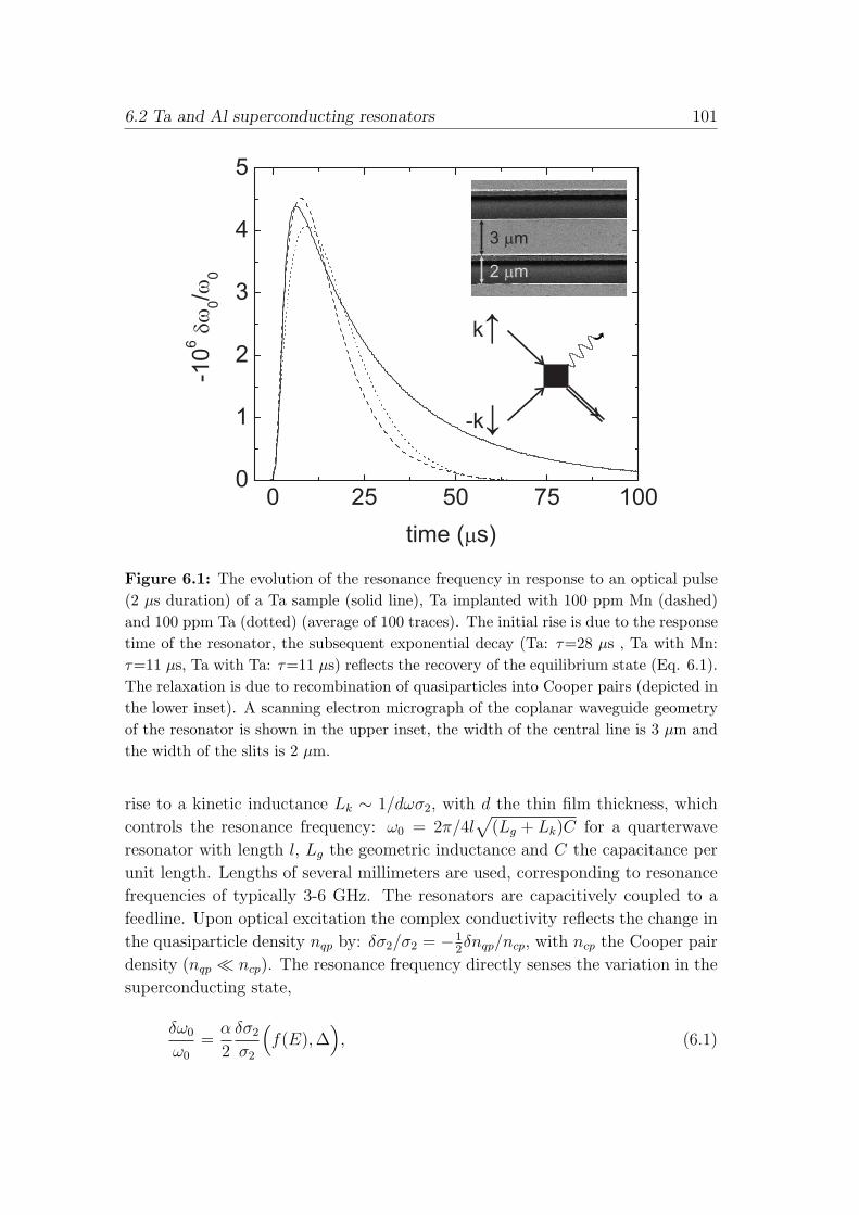
6.2 Ta and Al superconducting resonators 101
k↑
-k↓
3 mm
2 mm
Figure 6.1: The evolution of the resonance frequency in response to an optical pulse(2 µs duration) of a Ta sample (solid line), Ta implanted with 100 ppm Mn (dashed)and 100 ppm Ta (dotted) (average of 100 traces). The initial rise is due to the responsetime of the resonator, the subsequent exponential decay (Ta: τ=28 µs , Ta with Mn:τ=11 µs, Ta with Ta: τ=11 µs) reflects the recovery of the equilibrium state (Eq. 6.1).The relaxation is due to recombination of quasiparticles into Cooper pairs (depicted inthe lower inset). A scanning electron micrograph of the coplanar waveguide geometryof the resonator is shown in the upper inset, the width of the central line is 3 µm andthe width of the slits is 2 µm.
rise to a kinetic inductance Lk ∼ 1/dωσ2, with d the thin film thickness, which
controls the resonance frequency: ω0 = 2π/4l√
(Lg + Lk)C for a quarterwave
resonator with length l, Lg the geometric inductance and C the capacitance per
unit length. Lengths of several millimeters are used, corresponding to resonance
frequencies of typically 3-6 GHz. The resonators are capacitively coupled to a
feedline. Upon optical excitation the complex conductivity reflects the change in
the quasiparticle density nqp by: δσ2/σ2 = −12δnqp/ncp, with ncp the Cooper pair
density (nqp ¿ ncp). The resonance frequency directly senses the variation in the
superconducting state,
δω0
ω0
=α
2
δσ2
σ2
(f(E), ∆
), (6.1)
102 Chapter 6. Enhancement of quasiparticle recombination
with f(E) the distribution of quasiparticles over the energy and α the fraction
of the kinetic to total inductance.
The resonators are made from Ta and Al. The Ta film, 280 nm thick, is
sputter-deposited onto a hydrogen passivated, high resistivity (> 10 kΩcm) (100)-
oriented Si substrate. A 6 nm Nb seed layer is used underneath the Ta layer to
promote growth of the desired body-centered-cubic phase [12]. The film critical
temperature is 4.4 K, the low temperature resistivity (ρ) is 8.8 µΩcm and the
residual resistance ratio (RRR) is 3.2. The Al film, with a thickness of 100 nm, is
sputtered onto a similar Si substrate (Tc=1.2 K, ρ=0.81 µΩcm and RRR=4.5).
Patterning is done using optical lithography, followed by reactive ion etching for
Ta and wet etching for Al. After patterning various concentrations of Mn, as
magnetic atom, and Ta and Al have been ion-implanted. The Ta film has been
implanted with Mn, Ta and Al at energies of 500, 500 and 250 keV respectively,
and the Al film has been implanted with Mn and Al at 60 and 30 keV, to place
the peak of the concentration near the middle of the film [13]. The Ta samples
are placed on a He-3 sorption cooler in a He-4 cryostat, with the sample space
surrounded by a superconducting magnetic shield. The Al samples are placed on
an adiabatic demagnetization refrigerator; here a superconducting and cryoperm
shield are used. The optical pulse is provided by a GaAsP (1.9 eV) LED, which is
fibre-optically coupled to the sample box. The transmission of the feedline near
the resonance frequency is sensed using a signal generator, low noise amplifier
and quadrature mixer, allowing for monitoring the resonance frequency in the
time domain [2, 11].
6.3 Enhancement of low temperature recombi-
nation
Typical optical pulse responses are shown in Fig. 6.1 for Ta quarterwave res-
onators at the base temperature of 325 mK. The exponential decrease reflects
the restoration of equilibrium in the superconducting state. The initial rise is
due to the response time of the resonator. The faster decay indicates a faster
relaxation for implanted Ta samples. The temperature dependence of the re-
laxation times is shown in Fig. 6.2 for Ta samples implanted with a range of
concentrations from 0 to 100 ppm Mn, and with 100 ppm Ta and Al. At low
temperatures a clear trend of a decreasing relaxation time with increasing im-
purity concentration is visible, both for samples implanted with Mn as well as
with Ta and Al. Below T/Tc ∼ 0.1 the relaxation times become independent
of temperature, reaching plateau values of 26 µs for the unimplanted samples,

6.3 Enhancement of low temperature recombination 103
0.06 0.31
10
0 25 50 75 1000
10
20
30
base
tem
pera
ture
rela
xatio
n tim
e (
s)
concentration (ppm)
Ta
rela
xatio
n tim
e (
s)
reduced temperature - T/Tc
Figure 6.2: The relaxation time as a function of reduced bath temperature in Ta(Tc=4.4 K) with ion-implanted concentrations of Mn: 0 (¥), 10 (l), 20 (N), 50 (H)and 100 ppm (u), as well as with 100 ppm Ta (¤) and 100 ppm Al (#). The relaxationtimes at base temperature (325 mK) are plotted in the inset versus ion concentration.
values down to 11 µs for samples implanted with Mn, 11 µs with Ta and 16 µs
with Al, clearly decreasing with increasing impurity concentration (see inset).
Near T/Tc ∼ 0.15 the relaxation times reach a peak value in all samples. At
high temperatures (T/Tc & 0.2) we find that the relaxation times increase with
decreasing temperature. Here, the relaxation times of the implanted samples,
except for the sample with 100 ppm Mn, join with the values of the unimplanted
sample, and is understood as due to the conventional electron-phonon process
[2]. The critical temperature remains unchanged.
In Al samples, halfwave resonators, implanted with 0 to 100 ppm Mn or 100
ppm Al the relaxation times follow a similar pattern, see Fig. 6.3. The effect of
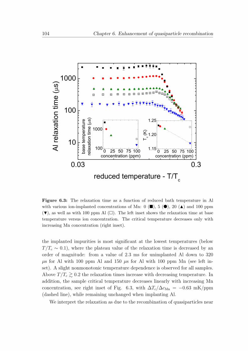
104 Chapter 6. Enhancement of quasiparticle recombination
0.03 0.3
10
100
1000
0 25 50 75 1001.15
1.20
1.25
T c (K)
concentration (ppm)0 25 50 75 100100
1000
base
tem
pera
ture
rela
xatio
n tim
e (
s)
concentration (ppm)
A
l rel
axat
ion
time
(s)
reduced temperature - T/Tc
Figure 6.3: The relaxation time as a function of reduced bath temperature in Alwith various ion-implanted concentrations of Mn: 0 (¥), 5 (l), 20 (N) and 100 ppm(H), as well as with 100 ppm Al (¤). The left inset shows the relaxation time at basetemperature versus ion concentration. The critical temperature decreases only withincreasing Mn concentration (right inset).
the implanted impurities is most significant at the lowest temperatures (below
T/Tc ∼ 0.1), where the plateau value of the relaxation time is decreased by an
order of magnitude: from a value of 2.3 ms for unimplanted Al down to 320
µs for Al with 100 ppm Al and 150 µs for Al with 100 ppm Mn (see left in-
set). A slight nonmonotonic temperature dependence is observed for all samples.
Above T/Tc & 0.2 the relaxation times increase with decreasing temperature. In
addition, the sample critical temperature decreases linearly with increasing Mn
concentration, see right inset of Fig. 6.3, with ∆Tc/∆cMn = −0.63 mK/ppm
(dashed line), while remaining unchanged when implanting Al.
We interpret the relaxation as due to the recombination of quasiparticles near
6.4 Conventional pair breaking and pair weakening theory 105
the gap energy: First, we probe σ2 which is associated with the Cooper pairs. Sec-
ond, identical relaxation times are found when creating quasiparticle excitations
near the gap energy by applying a microwave pulse at the resonance frequency
ω0. In addition, the data are not influenced by quasiparticle outdiffusion as no
length dependence was observed in the Al half wavelength resonators, where the
central line is isolated from the groundplane, and Ta quarter wavelength res-
onators used. Moreover, the relaxation time is independent of the photon flux
for the small intensities used. Furthermore, the samples are well isolated from
thermal radiation: we observe no significant change in relaxation time when vary-
ing the temperature of the cryostat or of a blackbody placed next to the sample
box. Finally, the significant effect of the implantation of impurities indicates that
the relaxation time reflects the restoration of equilibrium in the superconducting
films.
The data show a clear trend of decreasing relaxation time in both Ta and
Al with an increasing ion-implanted impurity concentration. The significant de-
crease at the lowest temperatures indicates that the dominant low temperature
relaxation channel is enhanced while the relaxation process at higher tempera-
tures is less affected.
6.4 Conventional pair breaking and pair weak-
ening theory
In a superconductor the magnetic nature of the atom depends on the coupling
between its spin and the host conduction electrons. Mn has been shown to retain
its magnetic moment in Nb, V [14] and Pb [8], acting as pair breaker and giving
rise to subgap states. On the other hand, when Mn is placed inside Al s−d mixing
occurs: the localized d electron states of the transition metal impurity strongly
mix with the conduction band, resulting in the impurity effectively loosing its
magnetic moment as well as an increase in the Coulomb repulsion [15]. It acts
predominantly as pair weakener: suppressing superconductivity, yet contrary to
the case of pair breaking, showing no evidence of subgap states [16].
In order to quantify a possible influence of magnetic impurities on recombina-
tion we use the conventional theories by Zittartz, Bringer and Muller-Hartmann
[17] and Kaiser [15]. In the presence of pair-breaking impurity bound states de-
velop within the energy gap near reduced energy γ. The quasiparticle excitations,
denoted by the Green’s function G, and the paired electrons, F , are described
by: E = u(∆+Γ√
1−u2
u2−γ2 ), with G(E) = u(E)/√
u(E)2 − 1, F (E) = i/√
u(E)2 − 1
and Γ = ~/τsf the pair-breaking parameter. For γ → 1 the Abrikosov-Gorkov
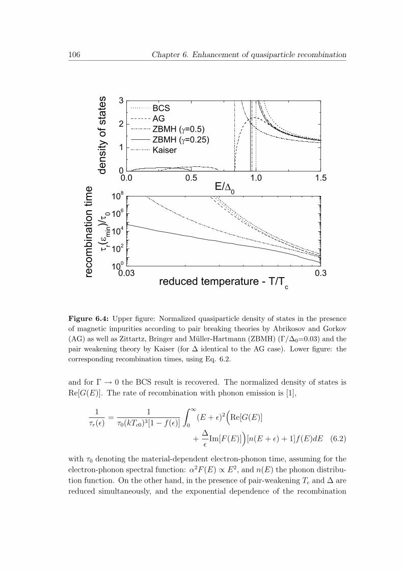
106 Chapter 6. Enhancement of quasiparticle recombination
0.03 0.3100
102
104
106
108
reco
mbi
natio
n tim
e
r(m
in)/
0
reduced temperature - T/Tc
0.0 0.5 1.0 1.50
1
2
3 BCS AG ZBMH ( =0.5) ZBMH ( =0.25) Kaiser
dens
ity o
f sta
tes
E/ 0
Figure 6.4: Upper figure: Normalized quasiparticle density of states in the presenceof magnetic impurities according to pair breaking theories by Abrikosov and Gorkov(AG) as well as Zittartz, Bringer and Muller-Hartmann (ZBMH) (Γ/∆0=0.03) and thepair weakening theory by Kaiser (for ∆ identical to the AG case). Lower figure: thecorresponding recombination times, using Eq. 6.2.
and for Γ → 0 the BCS result is recovered. The normalized density of states is
Re[G(E)]. The rate of recombination with phonon emission is [1],
1
τr(ε)=
1
τ0(kTc0)3[1− f(ε)]
∫ ∞
0
(E + ε)2(Re[G(E)]
+∆
εIm[F (E)]
)[n(E + ε) + 1]f(E)dE (6.2)
with τ0 denoting the material-dependent electron-phonon time, assuming for the
electron-phonon spectral function: α2F (E) ∝ E2, and n(E) the phonon distribu-
tion function. On the other hand, in the presence of pair-weakening Tc and ∆ are
reduced simultaneously, and the exponential dependence of the recombination
6.5 The role of disorder 107
time on T/Tc is retained. In Fig. 6.4, the density of states (upper figure) and
the recombination time for quasiparticles at the minimum excitation energy εmin
(lower figure) are shown for different cases. Clearly, a density of states modified
by magnetic impurities results in a recombination time which remains tempera-
ture dependent, independent of the model used. A particular model-analysis has
recently been performed by Kozorezov et al. [18].
6.5 The role of disorder
We conclude that the recombination processes are unrelated to the bulk mag-
netic moment of the implanted atoms, in agreement with the observation that
an enhancement can also be established by implanting nonmagnetic atoms (Figs.
6.1, 6.2 and 6.3). Instead we attribute the enhancement to an increase of the
disorder caused by the implantation. Impurities might alter the electron-phonon
interaction [19], τ0 in Eq. 6.2, but no saturation would result [2].
An interesting role of disorder, in particular at the surface, has recently
become apparent through phenomena controlled by unpaired magnetic surface
spins. An enhancement of the critical current of nanowires has been observed
[20], in agreement with theoretical predictions in which surface spins are aligned
by the magnetic field [21]. In addition, recent tunneling measurements on nio-
bium surfaces show subgap states, Fig. 6.4, signalling spins at the surface, pos-
sibly due to the native oxide [22]. Magnetic moments at surface defects have
also been proposed by Koch et al. [23] to explain the ubiquitous presence of
flux noise in SQUIDs. Sendelbach et al. [24] have observed in both Al and Nb
SQUIDs a strong dependence of the flux on temperature, which they interpret
as due to paramagnetic ordering of surface spins by local fields in the vortex
cores. In our recent experiments on the frequency noise of superconducting res-
onators we also find a strong dependence on the surface properties [25]. In view
of the other experiments, we conjecture that in our samples unpaired surface
spins are present, whose density is enhanced by the ion bombardment. In order
to properly address the relation to the recombination rate, Eq. 6.2 needs to be
reanalyzed taking into account spin flip [26], possible spin glass formation [24]
and particle-hole asymmetry [7], giving rise to quasiparticles in the ground state
[27].
In conclusion, we have measured the relaxation time in Ta and Al supercon-
ducting films implanted with both magnetic and nonmagnetic impurities, using
the complex conductivity. We find a clear trend of decreasing relaxation time
with increasing implanted impurity concentration, independent of their magnetic
108 Chapter 6. Enhancement of quasiparticle recombination
moment. Our observations show that low temperature quasiparticle recombina-
tion is enhanced by disorder, most likely involving the surface.
References
[1] S. B. Kaplan, C. C. Chi, D. N. Langenberg, J. J. Chang, S. Jafarey, and D. J.Scalapino, Quasiparticle and phonon lifetimes in superconductors, Phys. Rev. B14, 4854 (1976).
[2] R. Barends, J. J. A. Baselmans, S. J. C. Yates, J. R. Gao, J. N. Hovenier, and T.M. Klapwijk, Quasiparticle relaxation in optically excited high-Q superconductingresonators, Phys. Rev. Lett. 100, 257002 (2008).
[3] A. V. Timofeev, C. Pascual Garcıa, N. B. Kopnin, A. M. Savin, M. Meschke,F. Giazotto, and J. P. Pekola, Recombination-Limited Energy Relaxation in aBardeen-Cooper-Schrieffer Superconductor, Phys. Rev. Lett. 102, 017003 (2009).
[4] A. Anthore, F. Pierre, H. Pothier, and D. Esteve, Magnetic-field-dependent quasi-particle energy relaxation in mesoscopic wires, Phys. Rev. Lett. 90, 076806 (2003).
[5] B. Huard, A. Anthore, N. O. Birge, H. Pothier, and D. Esteve, Effect of magneticimpurities on energy exchange between electrons, Phys. Rev. Lett. 95, 036802(2005).
[6] A. A. Abrikosov and L. P. Gorkov, Contribution to the theory of superconductingalloys with paramagnetic impurities, Sov. Phys. JETP 12, 1243 (1961).
[7] A. Yazdani, B. A. Jones, C. P. Lutz, M. F. Crommie, and D. M. Eigler, Probingthe local effects of magnetic impurities on superconductivity, Science 275, 1767(1997).
[8] W. Bauriedl, P. Ziemann, and W. Buckel, Electron-Tunneling Observation of Im-purity Bands in Superconducting Manganese-Implanted Lead, Phys. Rev. Lett. 47,1163 (1981).
[9] L. Dumoulin, E. Guyon, and P. Nedellec, Tunneling study of localized bands insuperconductors with magnetic impurities (normal Kondo alloys in the supercon-ducting proximity), Phys. Rev. B 16, 1086 (1977).
[10] D. C. Mattis and J. Bardeen, Theory of the anomalous skin effect in normal andsuperconducting metals, Phys. Rev. 111, 412 (1958).
[11] P. K. Day, H. G. LeDuc, B. A. Mazin, A. Vayonakis, and J. Zmuidzinas, A broad-band superconducting detector suitable for use in large arrays, Nature 425, 817(2003).
[12] D. W. Face and D. E. Prober, Nucleation of body-centered-cubic tantalum filmswith a thin niobium underlayer, J. Vac. Sci. Tech. A 5, 3408 (1987).

References 109
[13] J. F. Ziegler et al., computer code SRIM-2008.01, www.srim.org, 2008.
[14] A. Roy, D. S. Buchanan, D. J. Holmgren, and D. M. Ginsberg, Localized magneticmoments on chromium and manganese dopant atoms in niobium and vanadium,Phys. Rev. B 31, 3003 (1985).
[15] A. B. Kaiser, Effect of non-magnetic localized states in superconducting alloys, J.Phys. C 3, 410 (1970).
[16] G. O’Neil, D. Schmidt, N. A. Miller, J. N. Ullom, A. Williams, G. B. Arnold,and S. T. Ruggiero, Observation of Nonmagnetic Resonant Scattering Effects byTunneling in Dilute Al-Mn Alloy Superconductors, Phys. Rev. Lett. 100, 056804(2008).
[17] J. Zittartz, A. Bringer, and E. Muller-Hartmann, Impurity bands in superconduc-tors with magnetic impurities, Solid State Comm. 10, 513 (1972).
[18] A. G. Kozorezov, A. A. Golubov, J. K. Wigmore, D. Martin, P. Verhoeve, R. A.Hijmering, and I. Jerjen, Inelastic scattering of quasiparticles in a superconductorwith magnetic impurities, Phys. Rev. B 78, 174501 (2008).
[19] J. Rammer and A. Schmid, Destruction of phase coherence by electron-phononinteractions in disordered conductors, Phys. Rev. B 34, 1352 (1986).
[20] A. Rogachev, T. C. Wei, D. Pekker, A. T. Bollinger, P. M. Goldbart, and A.Bezryadin, Magnetic-field enhancement of superconductivity in ultranarrow wires,Phys. Rev. Lett. 97, 137001 (2006).
[21] M. Yu. Kharitonov and M. V. Feigel’man, Enhancement of Superconductivity inDisordered Films by Parallel Magnetic Field, JETP Lett. 82, 421 (2005).
[22] T. Proslier, J. F. Zasadzinski, L. Cooley, C. Antoine, J. Moore, J. Norem, M.Pellin, and K. E. Gray, Tunneling study of cavity grade Nb: Possible magneticscattering at the surface, Appl. Phys. Lett. 92, 212505 (2008).
[23] R. H. Koch, D. P. DiVincenzo, and J. Clarke, Model for 1/f flux noise in SQUIDsand qubits, Phys. Rev. Lett. 98, 267003 (2007).
[24] S. Sendelbach, D. Hover, A. Kittel, M. Muck, J. M. Martinis, and R. McDermott,Magnetism in SQUIDs at millikelvin temperatures, Phys. Rev. Lett. 100, 227006(2008).
[25] R. Barends, H. L. Hortensius, T. Zijlstra, J. J. A. Baselmans, S. J. C. Yates, J.R. Gao, and T. M. Klapwijk, Contribution of dielectrics to frequency and noise ofNbTiN superconducting resonators, Appl. Phys. Lett. 92, 223502 (2008).
[26] C. Grimaldi and P. Fulde, Spin-Orbit Scattering Effects on the Phonon Emissionand Absorption in Superconducting Tunneling Junctions, Phys. Rev. Lett. 77,2550 (1996).
110 Chapter 6. Enhancement of quasiparticle recombination
[27] M. E. Flatte and J. M. Byers, Local electronic structure of defects in superconduc-tors, Phys. Rev. B 56, 11213 (1997).
Chapter 7
Contribution of dielectrics to frequency
and noise of NbTiN superconducting
resonators
We study NbTiN resonators by measurements of the temperature dependent
resonance frequency and frequency noise. Additionally, resonators are studied
covered with SiOx dielectric layers of various thicknesses. The resonance fre-
quency develops a non-monotonic temperature dependence with increasing SiOx
layer thickness. The increase in the noise is independent of the SiOx thickness,
demonstrating that the noise is not dominantly related to the low temperature
resonance frequency deviations.
This chapter is published as R. Barends, H. L. Hortensius, T. Zijlstra, J. J. A. Baselmans,S. J. C. Yates, J. R. Gao and T. M. Klapwijk, Appl. Phys. Lett. 92, 223502 (2008).
111
112 Chapter 7. Contribution of dielectrics to frequency and noise
7.1 NbTiN superconducting resonators for prob-
ing dielectrics
The interest in the low temperature properties of superconducting resonators for
photon detection [1, 2], quantum computation [3, 4] and quasiparticle relaxation
experiments [5] increases. In principle these properties are determined by the
superconductor, but in practice excess noise and low temperature deviations in
the resonance frequency have been observed, which are attributed to dielectrics.
It is understood that two-level systems (TLS) in dielectrics in the active region
of resonators contribute to limiting the quality factor and phase coherence, cause
noise and affect the permittivity ε [6, 7, 8, 9]. In order to identify the physical
mechanisms through which two-level systems in dielectrics affect the microwave
properties of superconducting films, we have chosen to study NbTiN resonators
with various coverages of SiOx. We find that NbTiN follows the Mattis-Bardeen
theory for the complex conductivity more closely than any of the other previously
used superconductors (Nb, Ta and Al) [10]. We demonstrate that deviations from
the ideal superconducting properties can be generated by covering the resonators
with a thin amorphous dielectric layer. In addition, we find that this dielectric
layer affects the noise and the permittivity differently.
We have made thin film NbTiN coplanar waveguide (CPW) quarter wave-
length resonators. The resonator (see lower inset Fig. 7.1) is formed by a central
line, 3 µm wide, and slits of 2 µm wide, with a NbTiN film thickness of 300
nm. The resonator is capacitively coupled to the feedline by placing the open
end alongside it. The complex conductivity σ1 − iσ2, with σ1 reflecting the con-
ductivity by quasiparticles and σ2 arising from the accelerative response of the
Cooper pair condensate, leads to a kinetic inductance Lk ∝ 1/d2πfσ2 for thin
films with thickness d [10, 11]. The resonance frequency is controlled by the ki-
netic inductance and permittivity, f0 = 1/4l√
(Lg + Lk)C(ε), with l the length
of the central line and Lg the geometric inductance and C ∝ ε the capacitance
per unit length. The resonance frequency is therefore a direct probe for both the
complex conductivity and the permittivity,
δf0
f0
=α
2
δσ2
σ2
− F
2
δε
ε, (7.1)
with α = Lk/(Lg + Lk) the kinetic inductance fraction and F a factor which
takes into account the active part of the resonator filled with the dielectric, as
argued by Gao et al. [9]. Resonance frequencies lie between 3-6 GHz. Near
the resonance frequency the forward transmission of the feedline S21 shows a dip
in the magnitude when measured as a function of the microwave frequency f
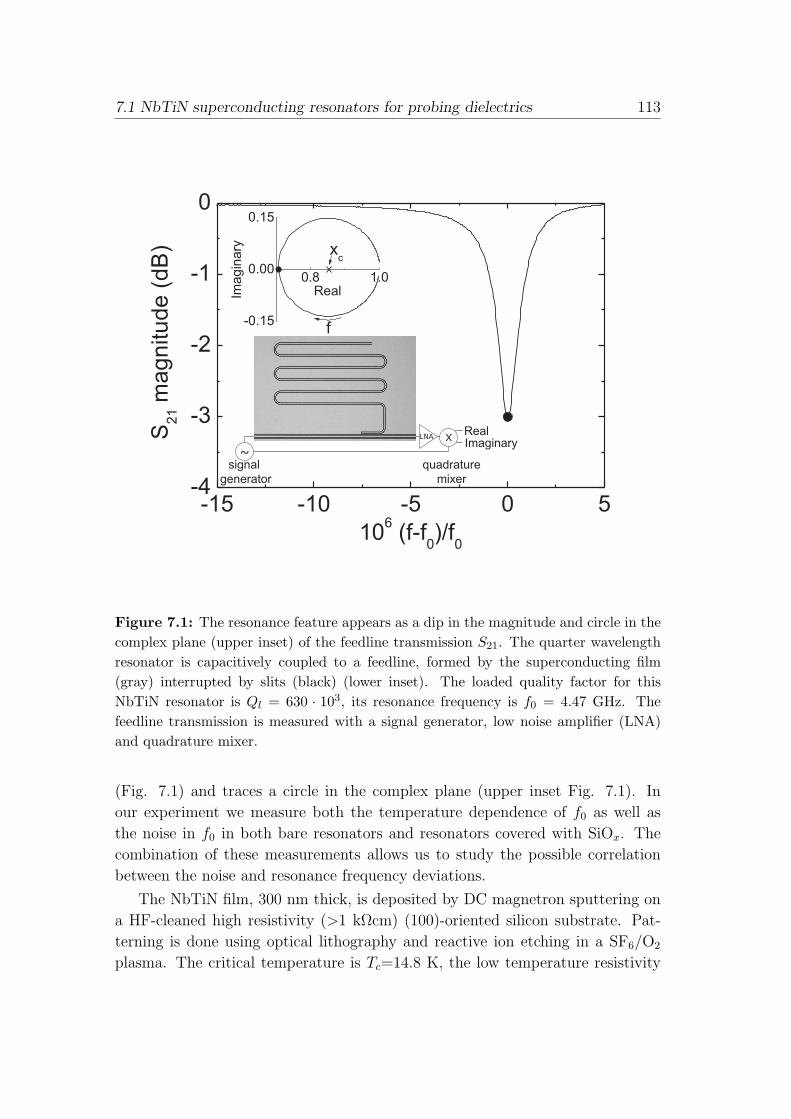
7.1 NbTiN superconducting resonators for probing dielectrics 113
1 2
quadrature
mixer
RealImaginary
X
signal
generator
LNA
~
-15 -10 -5 0 5-4
-3
-2
-1
0
0.8 1.0
-0.15
0.00
0.15
Imag
inary
Real
xc
f
S21
ma
gn
itu
de
(dB
)
106
(f-f0)/f
0
Figure 7.1: The resonance feature appears as a dip in the magnitude and circle in thecomplex plane (upper inset) of the feedline transmission S21. The quarter wavelengthresonator is capacitively coupled to a feedline, formed by the superconducting film(gray) interrupted by slits (black) (lower inset). The loaded quality factor for thisNbTiN resonator is Ql = 630 · 103, its resonance frequency is f0 = 4.47 GHz. Thefeedline transmission is measured with a signal generator, low noise amplifier (LNA)and quadrature mixer.
(Fig. 7.1) and traces a circle in the complex plane (upper inset Fig. 7.1). In
our experiment we measure both the temperature dependence of f0 as well as
the noise in f0 in both bare resonators and resonators covered with SiOx. The
combination of these measurements allows us to study the possible correlation
between the noise and resonance frequency deviations.
The NbTiN film, 300 nm thick, is deposited by DC magnetron sputtering on
a HF-cleaned high resistivity (>1 kΩcm) (100)-oriented silicon substrate. Pat-
terning is done using optical lithography and reactive ion etching in a SF6/O2
plasma. The critical temperature is Tc=14.8 K, the low temperature resistivity
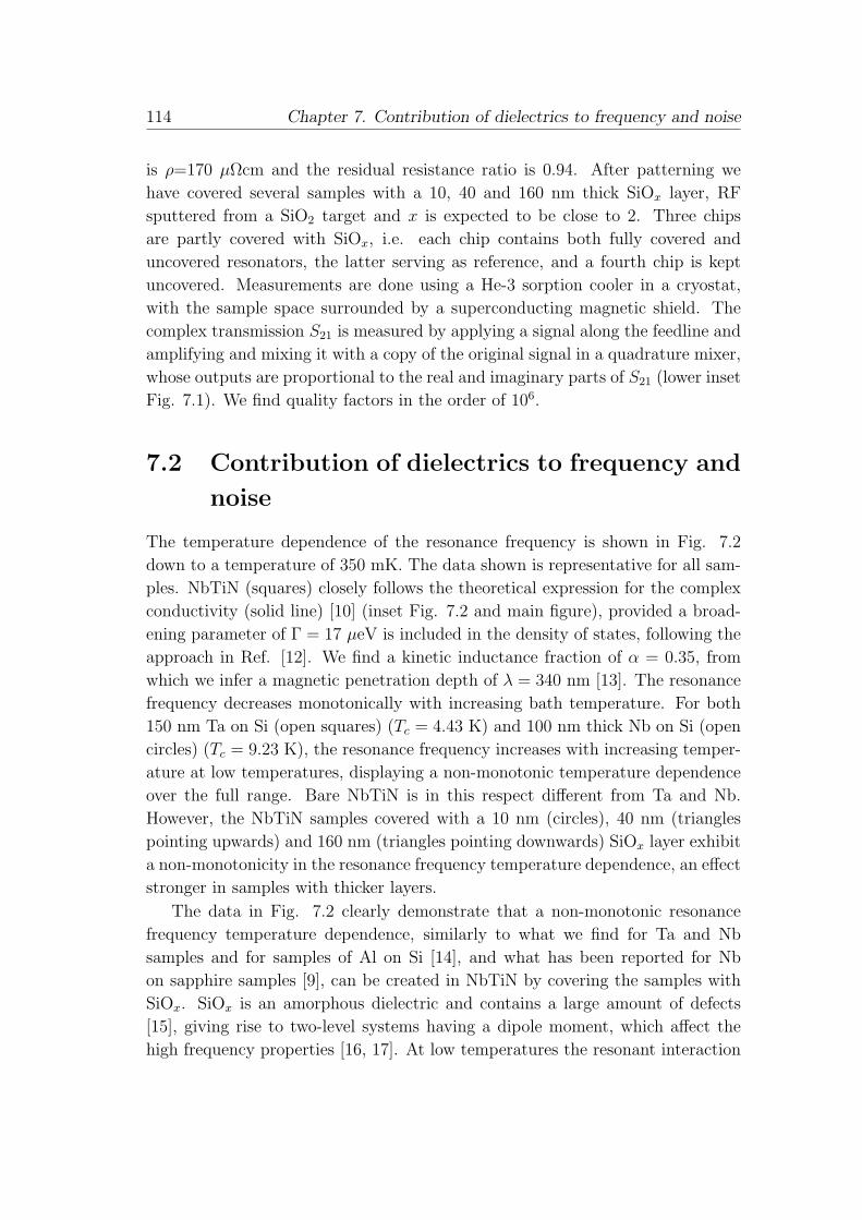
114 Chapter 7. Contribution of dielectrics to frequency and noise
is ρ=170 µΩcm and the residual resistance ratio is 0.94. After patterning we
have covered several samples with a 10, 40 and 160 nm thick SiOx layer, RF
sputtered from a SiO2 target and x is expected to be close to 2. Three chips
are partly covered with SiOx, i.e. each chip contains both fully covered and
uncovered resonators, the latter serving as reference, and a fourth chip is kept
uncovered. Measurements are done using a He-3 sorption cooler in a cryostat,
with the sample space surrounded by a superconducting magnetic shield. The
complex transmission S21 is measured by applying a signal along the feedline and
amplifying and mixing it with a copy of the original signal in a quadrature mixer,
whose outputs are proportional to the real and imaginary parts of S21 (lower inset
Fig. 7.1). We find quality factors in the order of 106.
7.2 Contribution of dielectrics to frequency and
noise
The temperature dependence of the resonance frequency is shown in Fig. 7.2
down to a temperature of 350 mK. The data shown is representative for all sam-
ples. NbTiN (squares) closely follows the theoretical expression for the complex
conductivity (solid line) [10] (inset Fig. 7.2 and main figure), provided a broad-
ening parameter of Γ = 17 µeV is included in the density of states, following the
approach in Ref. [12]. We find a kinetic inductance fraction of α = 0.35, from
which we infer a magnetic penetration depth of λ = 340 nm [13]. The resonance
frequency decreases monotonically with increasing bath temperature. For both
150 nm Ta on Si (open squares) (Tc = 4.43 K) and 100 nm thick Nb on Si (open
circles) (Tc = 9.23 K), the resonance frequency increases with increasing temper-
ature at low temperatures, displaying a non-monotonic temperature dependence
over the full range. Bare NbTiN is in this respect different from Ta and Nb.
However, the NbTiN samples covered with a 10 nm (circles), 40 nm (triangles
pointing upwards) and 160 nm (triangles pointing downwards) SiOx layer exhibit
a non-monotonicity in the resonance frequency temperature dependence, an effect
stronger in samples with thicker layers.
The data in Fig. 7.2 clearly demonstrate that a non-monotonic resonance
frequency temperature dependence, similarly to what we find for Ta and Nb
samples and for samples of Al on Si [14], and what has been reported for Nb
on sapphire samples [9], can be created in NbTiN by covering the samples with
SiOx. SiOx is an amorphous dielectric and contains a large amount of defects
[15], giving rise to two-level systems having a dipole moment, which affect the
high frequency properties [16, 17]. At low temperatures the resonant interaction
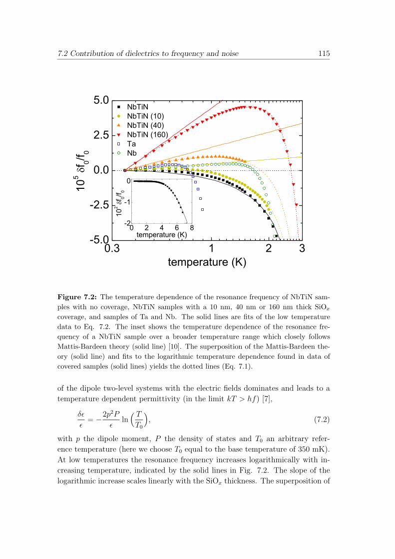
7.2 Contribution of dielectrics to frequency and noise 115
0.3 1 2 3-5.0
-2.5
0.0
2.5
5.0
0 2 4 6 8-2
-1
0
102
f 0/f 0
temperature (K)
NbTiNNbTiN (10)NbTiN (40)NbTiN (160)TaNb
105
f 0/f 0
temperature (K)
Figure 7.2: The temperature dependence of the resonance frequency of NbTiN sam-ples with no coverage, NbTiN samples with a 10 nm, 40 nm or 160 nm thick SiOx
coverage, and samples of Ta and Nb. The solid lines are fits of the low temperaturedata to Eq. 7.2. The inset shows the temperature dependence of the resonance fre-quency of a NbTiN sample over a broader temperature range which closely followsMattis-Bardeen theory (solid line) [10]. The superposition of the Mattis-Bardeen the-ory (solid line) and fits to the logarithmic temperature dependence found in data ofcovered samples (solid lines) yields the dotted lines (Eq. 7.1).
of the dipole two-level systems with the electric fields dominates and leads to a
temperature dependent permittivity (in the limit kT > hf) [7],
δε
ε= −2p2P
εln
( T
T0
), (7.2)
with p the dipole moment, P the density of states and T0 an arbitrary refer-
ence temperature (here we choose T0 equal to the base temperature of 350 mK).
At low temperatures the resonance frequency increases logarithmically with in-
creasing temperature, indicated by the solid lines in Fig. 7.2. The slope of the
logarithmic increase scales linearly with the SiOx thickness. The superposition of
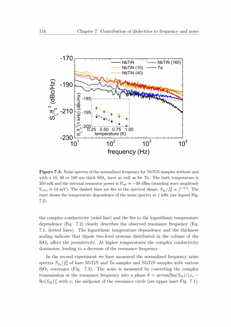
116 Chapter 7. Contribution of dielectrics to frequency and noise
101 102 103 104-230
-210
-190
-170
0.25 0.50 0.75 1.00-205
-195
-185
Sf 0/f 02 (1
kH
z) (d
Bc/
Hz)
temperature (K)
S
f 0/f 02 (dB
c/H
z)
frequency (Hz)
NbTiN NbTiN (10) NbTiN (40)
NbTiN (160) Ta
Figure 7.3: Noise spectra of the normalized frequency for NbTiN samples without andwith a 10, 40 or 160 nm thick SiOx layer as well as for Ta. The bath temperature is350 mK and the internal resonator power is Pint ≈ −30 dBm (standing wave amplitudeVrms ≈ 14 mV). The dashed lines are fits to the spectral shape, Sf0/f2
0 ∝ f−0.4. Theinset shows the temperature dependence of the noise spectra at 1 kHz (see legend Fig.7.2).
the complex conductivity (solid line) and the fits to the logarithmic temperature
dependence (Eq. 7.2) closely describes the observed resonance frequency (Eq.
7.1, dotted lines). The logarithmic temperature dependence and the thickness
scaling indicate that dipole two-level systems distributed in the volume of the
SiOx affect the permittivity. At higher temperatures the complex conductivity
dominates, leading to a decrease of the resonance frequency.
In the second experiment we have measured the normalized frequency noise
spectra Sf0/f20 of bare NbTiN and Ta samples and NbTiN samples with various
SiOx coverages (Fig. 7.3). The noise is measured by converting the complex
transmission at the resonance frequency into a phase θ = arctan[Im(S21)/(xc −Re(S21))] with xc the midpoint of the resonance circle (see upper inset Fig. 7.1).
References 117
The frequency is related to the phase by: θ = −4Qlδf0
f0, with Ql the resonator
loaded quality factor. The power spectral density is calculated by: Sf0/f20 =
Sθ/(4Ql)2. The noise spectra of samples of NbTiN, and NbTiN with a 10 nm,
40 nm and 160 nm thick SiOx layer follow Sf0/f20 ∝ f−0.4 (dashed) until a roll-
off at a frequency in the order of 10 kHz. The roll-off is due to the resonator-
specific response time and is a function of the loaded quality factor and resonance
frequency. We find that the noise is significantly increased by approximately
7 dBc/Hz as soon as the samples are covered by SiOx and that this increase
is independent of the further increase in SiOx layer thickness. This behavior
persists with increasing temperature, where the noise decreases (inset Fig. 7.3),
consistent with recent observations for Nb [18].
These measurements clearly show that the increase in the noise is indepen-
dent of the SiOx layer thickness, whereas the change in resonance frequency is
thickness dependent. It has recently been argued, in independent work [9, 19],
that the dielectric influences both the resonance frequency and the noise through
the capacitance. In this work we have demonstrated that indeed the resonance
frequency is controlled by the bulk of the dielectric. However, the observed noise
enhancement appears due to the interface. The latter suggests that it is related
to quasiparticle trapping and release at the interface, influencing the inductance
rather than the capacitance. We find that the noise of NbTiN samples covered
with SiOx has a spectral shape and temperature dependence which is very com-
parable to the noise of NbTiN samples without coverage and also of Ta samples.
In addition, the noise of NbTiN and Ta samples is very similar, while the tem-
perature dependence of the resonance frequency is significantly different. This
points towards an interpretation of the noise in terms of inductance fluctuations.
In summary, we conclude that the frequency noise and the low temperature
deviations in the resonance frequency of planar superconducting resonators are
differently dependent on two-level systems in dielectrics. Using NbTiN samples
and introducing dipole two-level systems by covering the samples with various
SiOx layer thicknesses we find that the logarithmic temperature dependent in-
crease in the resonance frequency scales with the layer thickness. The frequency
noise increases strongly as soon as a SiOx layer is present and is, in contrast to
the resonance frequency results, thickness independent.
References
[1] P. K. Day, H. G. LeDuc, B. A. Mazin, A. Vayonakis, and J. Zmuidzinas, A broad-band superconducting detector suitable for use in large arrays, Nature 425, 817(2003).

118 Chapter 7. Contribution of dielectrics to frequency and noise
[2] K. W. Lehnert, K. D. Irwin, M. A. Castellanos-Beltran, J. A. B. Mates, and L.R. Vale, Evaluation of a microwave SQUID multiplexer prototype, IEEE Trans.Appl. Sup. 17, 705 (2007).
[3] A. Wallraff, D. I. Schuster, A. Blais, L. Frunzio, R. S. Huang, J. Majer, S. Ku-mar, S. M. Girvin and R. J. Schoelkopf, Strong coupling of a single photon toa superconducting qubit using circuit quantum electrodynamics, Nature 431, 162(2004).
[4] A. Palacios-Laloy, F. Nguyen, F. Mallet, P. Bertet, D. Vion, and D. Esteve, Tun-able resonators for quantum circuits, J. Low Temp. Phys. 151, 1034 (2008).
[5] R. Barends, J. J. A. Baselmans, S. J. C. Yates, J. R. Gao, J. N. Hovenier, and T.M. Klapwijk, Quasiparticle relaxation in optically excited high-Q superconductingresonators, Phys. Rev. Lett. 100, 257002 (2008).
[6] J. M. Martinis, K. B. Cooper, R. McDermott, M. Steffen, M. Ansmann, K. D.Osborn, K. Cicak, S. Oh, D. P. Pappas, R. W. Simmonds, and C. C. Yu, Deco-herence in Josephson Qubits from Dielectric Loss, Phys. Rev. Lett. 95, 210503(2005).
[7] W. A. Phillips, Two-level states in glasses, Rep. Prog. Phys. 50, 1657 (1987).
[8] J. Gao, J. Zmuidzinas, B. A. Mazin, H. G. LeDuc, and P. K. Day, Noise propertiesof superconducting coplanar waveguide microwave resonators, Appl. Phys. Lett.90, 102507 (2007).
[9] J. Gao, M. Daal, A. Vayonakis, S. Kumar, J. Zmuidzinas, B. Sadoulet, B. A.Mazin, P. K. Day, and H. G. LeDuc, Experimental evidence for a surface distri-bution of two-level systems in superconducting lithographed microwave resonators,Appl. Phys. Lett. 92, 152505 (2008).
[10] D. C. Mattis and J. Bardeen, Theory of the anomalous skin effect in normal andsuperconducting metals, Phys. Rev. 111, 412 (1958).
[11] M. Tinkham, Introduction to Superconductivity (McGraw-Hill, New York, 1996).
[12] R. C. Dynes, V. Narayanamurti, and J. P. Garno, Direct Measurement of Quasiparticle-Lifetime Broadening in a Strong-Coupled Superconductor, Phys. Rev. Lett. 41,1509 (1978).
[13] J. C. Booth and C. L. Holloway, Conductor Loss in Superconducting Planar Struc-tures: Calculations and Measurements, IEEE Trans. Micr. Theory Tech. 47, 769(1999).
[14] J. J. A. Baselmans, S. J. C. Yates, R. Barends, Y. J. Y. Lankwarden, J. R. Gao,H. F. C. Hoevers, and T. M. Klapwijk, Noise and sensitivity of aluminum kineticinductance detectors for sub-mm astronomy, J. Low Temp. Phys. 151, 524 (2008).
[15] D. L. Griscom, Defect structure of glasses - some outstanding questions in regardto vitreous silica, J. Non-Crystalline Solids 73, 51 (1985).
References 119
[16] B. Golding, M. von Schickfus, S. Hunklinger, and K. Dransfeld, Intrinsic electricdipole moment of tunneling systems in silica glasses, Phys. Rev. Lett. 43, 1817(1979).
[17] M. von Schickfus and S. Hunklinger, Dielectric coupling of low-energy excitationsin vitreous silica to electromagnetic waves, J. Phys. C: Solid State Phys. 9, L439(1976).
[18] S. Kumar, J. Gao, J. Zmuidzinas, B. A. Mazin, H. G. LeDuc, and P. K. Day,Temperature dependence of the frequency and noise of superconducting coplanarwaveguide resonators, Appl. Phys. Lett. 92, 123503 (2008).
[19] J. Gao, M. Daal, J. M. Martinis, A. Vayonakis, J. Zmuidzinas, B. Sadoulet, B. A.Mazin, P. K. Day, and H. G. LeDuc, A semiempirical model for two-level systemnoise in superconducting microresonators, Appl. Phys. Lett. 92, 212504 (2008).

120 Chapter 7. Contribution of dielectrics to frequency and noise
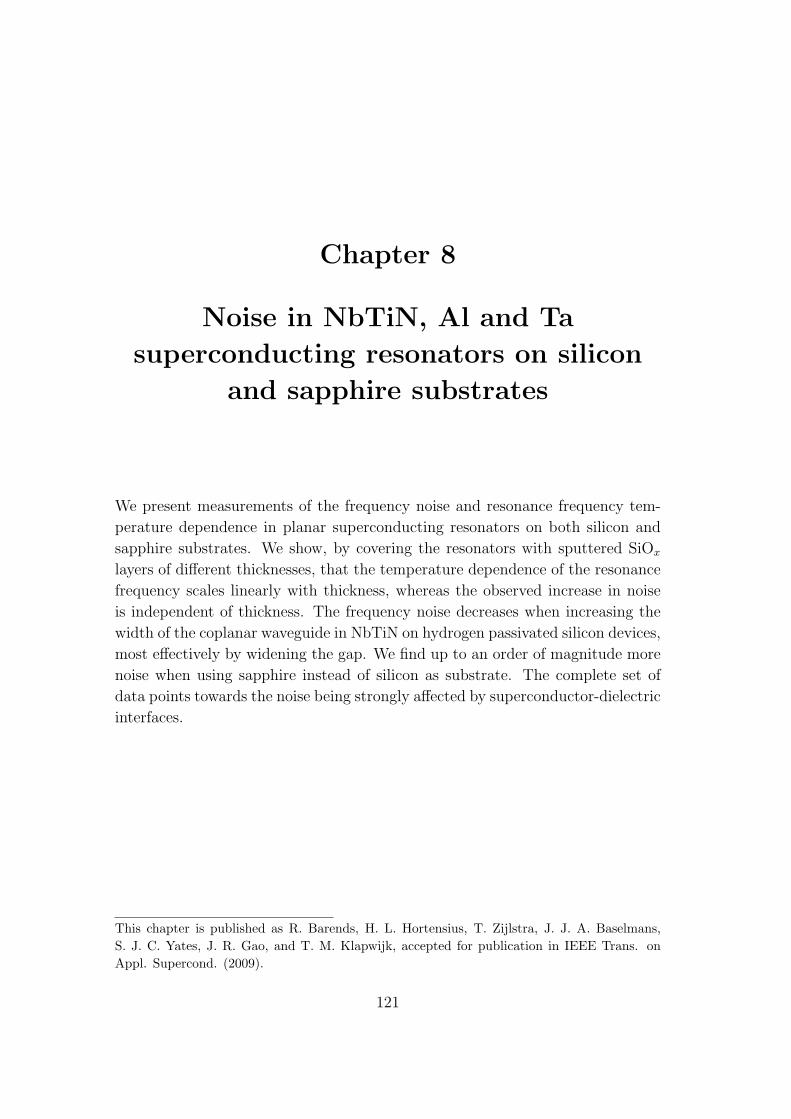
Chapter 8
Noise in NbTiN, Al and Ta
superconducting resonators on silicon
and sapphire substrates
We present measurements of the frequency noise and resonance frequency tem-
perature dependence in planar superconducting resonators on both silicon and
sapphire substrates. We show, by covering the resonators with sputtered SiOx
layers of different thicknesses, that the temperature dependence of the resonance
frequency scales linearly with thickness, whereas the observed increase in noise
is independent of thickness. The frequency noise decreases when increasing the
width of the coplanar waveguide in NbTiN on hydrogen passivated silicon devices,
most effectively by widening the gap. We find up to an order of magnitude more
noise when using sapphire instead of silicon as substrate. The complete set of
data points towards the noise being strongly affected by superconductor-dielectric
interfaces.
This chapter is published as R. Barends, H. L. Hortensius, T. Zijlstra, J. J. A. Baselmans,S. J. C. Yates, J. R. Gao, and T. M. Klapwijk, accepted for publication in IEEE Trans. onAppl. Supercond. (2009).
121

122 Chapter 8. Noise in NbTiN, Al and Ta superconducting resonators
8.1 Introduction
Superconducting resonators are becoming increasingly attractive for photon de-
tection [1] as well as for quantum computation [2]. Devices work well, showing
quality factors in the order of 106 [3], and exhibiting quasiparticle relaxation times
among the longest observed [4, 5], allowing for background limited photometry.
Presently we reach an electrical noise equivalent power (NEP ) as low as 6 ·10−19
W/√
Hz with Al resonators [6]. However, these resonators have ubiquitously
been found to generate significant frequency noise, irrespective of superconduct-
ing materials or substrates [7, 8]. The frequency noise is observed to exhibit very
comparable properties in all samples used: showing a 1/f∼0.4 spectrum (Fig.
8.1), decreasing with applied microwave power, following 1/P 0.5, and decreasing
with bath temperature, with 1/T 1.1 [8] or 1/T 1.7 [9]. The noise is a major issue
for low temperature applications and determines further gains in the sensitivity
of kinetic inductance photon detectors.
In independent work low temperature non-monotonic deviations in the reso-
nance frequency temperature dependence [10] and frequency noise [11] have been
observed in Nb on sapphire resonators. These results have been interpreted to
arise from dipole two-level systems in dielectrics in the active region of the res-
onator, which couple to the electric fields; the experimental data point towards
two-level systems distributed either on the surfaces of the superconducting film
and/or on the surface of the exposed substrate in the gaps. In the proposed
interpretation the low temperature resonance frequency deviations with temper-
ature are coupled to the noise, supported by the width scaling of the noise and
resonance frequency deviations with temperature [10, 11]. However, the vari-
ous processes arising in the volume of the thin surface layer or in the interface
between the superconductor and surface layer may contribute differently to the
noise and/or the resonance frequency variations with temperature.
8.2 Contribution of dielectric coverage
Recently, we have measured the noise and temperature dependent resonance fre-
quency in NbTiN superconducting resonators covered with a 10, 40 or 160 nm
thick amorphous dielectric SiOx layers [8]; the sample chips contain both fully
covered, i.e. both the superconducting film and the gaps, and fully uncovered
resonators. The nearby part of the feedline was covered or kept uncovered as well.
We find that the noise jumps to a higher level as soon as the samples are covered
with SiOx, independent of the layer thickness, see Fig. 8.1. Additionally, the de-
viations in the resonance frequency grow linearly with increasing layer thickness,
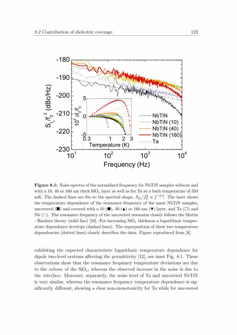
8.2 Contribution of dielectric coverage 123
101 102 103 104-230
-220
-210
-200
-190
-180
0.3 1 2 3-5
0
5
105
f 0/f 0
Temperature (K)
S
f 0/f 02 (dB
c/H
z)
Frequency (Hz)
NbTiN NbTiN (10) NbTiN (40) NbTiN (160) Ta
Figure 8.1: Noise spectra of the normalized frequency for NbTiN samples without andwith a 10, 40 or 160 nm thick SiOx layer as well as for Ta at a bath temperature of 350mK. The dashed lines are fits to the spectral shape, Sf0/f2
0 ∝ f−0.4. The inset showsthe temperature dependence of the resonance frequency of the same NbTiN samples,uncovered (¥) and covered with a 10 (l), 40 (N) or 160 nm (H) layer, and Ta (¤) andNb (#). The resonance frequency of the uncovered resonator closely follows the Mattis- Bardeen theory (solid line) [16]. For increasing SiOx thickness a logarithmic temper-ature dependence develops (dashed lines). The superposition of these two temperaturedependencies (dotted lines) closely describes the data. Figure reproduced from [8].
exhibiting the expected characteristic logarithmic temperature dependence for
dipole two-level systems affecting the permittivity [12], see inset Fig. 8.1. These
observations show that the resonance frequency temperature deviations are due
to the volume of the SiOx, whereas the observed increase in the noise is due to
the interface. Moreover, separately, the noise level of Ta and uncovered NbTiN
is very similar, whereas the resonance frequency temperature dependence is sig-
nificantly different, showing a clear non-monotonicity for Ta while for uncovered
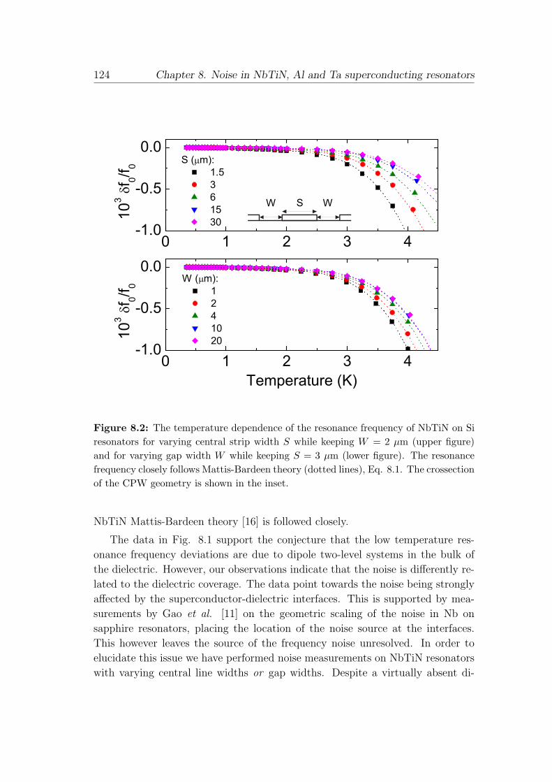
124 Chapter 8. Noise in NbTiN, Al and Ta superconducting resonators
0 1 2 3 4-1.0
-0.5
0.00 1 2 3 4
-1.0
-0.5
0.0S ( m):
1.5 3 6 15 30
103
f 0/f 0
Temperature (K)
W W
W ( m): 1 2 4 10 20
103
f 0/f 0
S
Figure 8.2: The temperature dependence of the resonance frequency of NbTiN on Siresonators for varying central strip width S while keeping W = 2 µm (upper figure)and for varying gap width W while keeping S = 3 µm (lower figure). The resonancefrequency closely follows Mattis-Bardeen theory (dotted lines), Eq. 8.1. The crossectionof the CPW geometry is shown in the inset.
NbTiN Mattis-Bardeen theory [16] is followed closely.
The data in Fig. 8.1 support the conjecture that the low temperature res-
onance frequency deviations are due to dipole two-level systems in the bulk of
the dielectric. However, our observations indicate that the noise is differently re-
lated to the dielectric coverage. The data point towards the noise being strongly
affected by the superconductor-dielectric interfaces. This is supported by mea-
surements by Gao et al. [11] on the geometric scaling of the noise in Nb on
sapphire resonators, placing the location of the noise source at the interfaces.
This however leaves the source of the frequency noise unresolved. In order to
elucidate this issue we have performed noise measurements on NbTiN resonators
with varying central line widths or gap widths. Despite a virtually absent di-

8.3 Experiment 125
electric surface layer, we find a very similar pattern: by increasing the width the
noise is reduced; most effectively by widening the gap. Additionally, we find that
the noise is increased when using sapphire as substrate instead of Si, indicating
that the choice of crystalline substrate affects the frequency noise.
8.3 Experiment
The NbTiN quarter wavelength superconducting resonators consist of a mean-
dering coplanar waveguide (CPW), coupled capacitively by placing the open
end alongside the feedline. The resonance frequency is given by: f0 = 1/4l√(Lg + Lk)C, with Lg and C the geometric inductance and capacitance per unit
length and l the resonator length. The kinetic inductance Lk arises from the
complex conductivity σ1 − iσ2 of the superconducting film, for films with arbi-
trary thickness d: Lk = µ0λ coth(d/λ) [13, 14], with λ ∝√
1/σ2 in the dirty
limit [15]. The imaginary part σ2 arises from the accelerative response of the
superconducting condensate, while the real part σ1 reflects conduction by the
quasiparticles [16]. The resonance frequency is a probe for the change in the
complex conductivity, in the dirty limit
δf0
f0
=αβ
4
δσ2
σ2
, (8.1)
with α = Lk/(Lg + Lk) the kinetic inductance fraction and β = 1 + 2d/λsinh(2d/λ)
; for
the bulk limit: β = 1, and for the thin film limit: β = 2. Near f0 the feedline
transmission shows a dip in the magnitude and a circle in the polar plane [1].
Resonance frequencies used lie between 3-9 GHz.
The NbTiN film, 300 nm thick, is sputter deposited on a high resistivity (>1
kΩcm) hydrogen passivated (HF-cleaned) (100)-oriented Si substrate. The film
critical temperature Tc is 14.7 K, the low temperature resistivity ρ is 160 µΩcm
and the residual resistance ratio RRR is 0.94. Alternatively, a 300 nm thick
NbTiN film is deposited on A-plane sapphire (Tc = 14.8 K, ρ = 150 µΩcm,
RRR = 0.98). Patterning is done using optical lithography and reactive ion
etching in a SF6/O2 plasma. We use central line widths S of 1.5, 3, 6, 15 and 30
µm while keeping the gap width W at 2 µm. Additionally, gap widths W of 1, 2,
4, 10 and 20 µm are used while keeping S = 3 µm. Scanning electron microscope
inspection, see inset Fig. 8.4, indicates the etched edges of the NbTiN film to be
vertical as desired. In addition, we find that the values for S are approximately
0.5 µm smaller than intended for both films, adding to the values of W . An
undercut of roughly 150 nm is present in the NbTiN on Si samples. The samples
are placed inside a gold plated Cu sample box, mounted on a He-3 sorption cooler
126 Chapter 8. Noise in NbTiN, Al and Ta superconducting resonators
-45 -40 -35 -30 -25 -20-220
-210
-200
-190-45 -40 -35 -30 -25 -20
-220
-210
-200
-190
4 10 20
Sf 0/f 02 (1
kH
z) (d
Bc/
Hz)
Internal resonator power (dBm)
S ( m): 1.5 3
W ( m): 1 2
6 30
Figure 8.3: The normalized frequency noise at 1 kHz of NbTiN on Si resonatorsfor varying central strip width (upper figure) and varying gap width (lower figure)versus internal resonator power, taking into account the changing impedance of theresonator waveguide (see text). The dotted lines are fits to the power dependence,Sf0/f2
0 ∝ P−0.5int . The bath temperature is 350 mK.
inside a cryostat. The sample space is surrounded by a superconducting shield.
The feedline transmission is sensed using a signal generator, low noise amplifier
and quadrature mixer. The frequency noise is obtained by measuring the feedline
transmission at the resonance frequency in the time domain and calculating the
power spectral density (for more details see [1, 4, 8]).
8.4 Noise width dependence
The temperature dependence of the resonance frequency for resonators of NbTiN
on Si is shown in Fig. 8.2 down to bath temperatures of 350 mK. For increas-
ing temperature the resonance frequency decreases monotonically, following the
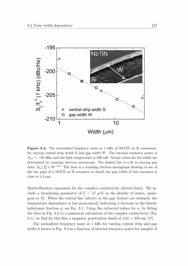
8.4 Noise width dependence 127
1 10-210
-205
-200
-195
central strip width S gap width W
S
f 0/f 02 (1 k
Hz)
(dB
c/H
z)
Width ( m)
Figure 8.4: The normalized frequency noise at 1 kHz of NbTiN on Si resonators,for varying central strip width S and gap width W . The internal resonator power isPint = −30 dBm and the bath temperature is 350 mK. Actual values for the width aredetermined by scanning electron microscopy. The dashed line is a fit to varying gapdata: Sf0/f2
0 ∝ W−0.6. The inset is a scanning electron micrograph showing of one ofthe two gaps of a NbTiN on Si resonator in detail; the gap width of this resonator isclose to 1.4 µm.
Mattis-Bardeen expression for the complex conductivity (dotted lines). We in-
clude a broadening parameter of Γ = 17 µeV in the density of states, analo-
gous to [8]. When the central line (above) or the gap (below) are widened, the
temperature dependence is less pronounced, indicating a decrease in the kinetic
inductance fraction α, see Eq. 8.1. Using the extracted values for α, by fitting
the data in Fig. 8.2 to a numerical calculation of the complex conductivity (Eq.
8.1), we find for this film a magnetic penetration depth of λ(0) = 350 nm [17].
The normalized frequency noise at 1 kHz for varying central strip and gap
width is shown in Fig. 8.3 as a function of internal resonator power for samples of
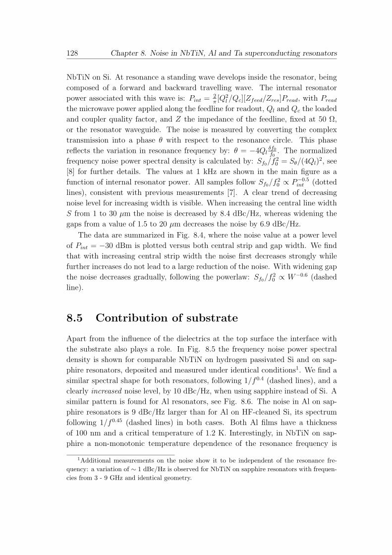
128 Chapter 8. Noise in NbTiN, Al and Ta superconducting resonators
NbTiN on Si. At resonance a standing wave develops inside the resonator, being
composed of a forward and backward travelling wave. The internal resonator
power associated with this wave is: Pint = 2π[Q2
l /Qc][Zfeed/Zres]Pread, with Pread
the microwave power applied along the feedline for readout, Ql and Qc the loaded
and coupler quality factor, and Z the impedance of the feedline, fixed at 50 Ω,
or the resonator waveguide. The noise is measured by converting the complex
transmission into a phase θ with respect to the resonance circle. This phase
reflects the variation in resonance frequency by: θ = −4Qlδf0
f0. The normalized
frequency noise power spectral density is calculated by: Sf0/f20 = Sθ/(4Ql)
2, see
[8] for further details. The values at 1 kHz are shown in the main figure as a
function of internal resonator power. All samples follow Sf0/f20 ∝ P−0.5
int (dotted
lines), consistent with previous measurements [7]. A clear trend of decreasing
noise level for increasing width is visible. When increasing the central line width
S from 1 to 30 µm the noise is decreased by 8.4 dBc/Hz, whereas widening the
gaps from a value of 1.5 to 20 µm decreases the noise by 6.9 dBc/Hz.
The data are summarized in Fig. 8.4, where the noise value at a power level
of Pint = −30 dBm is plotted versus both central strip and gap width. We find
that with increasing central strip width the noise first decreases strongly while
further increases do not lead to a large reduction of the noise. With widening gap
the noise decreases gradually, following the powerlaw: Sf0/f20 ∝ W−0.6 (dashed
line).
8.5 Contribution of substrate
Apart from the influence of the dielectrics at the top surface the interface with
the substrate also plays a role. In Fig. 8.5 the frequency noise power spectral
density is shown for comparable NbTiN on hydrogen passivated Si and on sap-
phire resonators, deposited and measured under identical conditions1. We find a
similar spectral shape for both resonators, following 1/f 0.4 (dashed lines), and a
clearly increased noise level, by 10 dBc/Hz, when using sapphire instead of Si. A
similar pattern is found for Al resonators, see Fig. 8.6. The noise in Al on sap-
phire resonators is 9 dBc/Hz larger than for Al on HF-cleaned Si, its spectrum
following 1/f 0.45 (dashed lines) in both cases. Both Al films have a thickness
of 100 nm and a critical temperature of 1.2 K. Interestingly, in NbTiN on sap-
phire a non-monotonic temperature dependence of the resonance frequency is
1Additional measurements on the noise show it to be independent of the resonance fre-quency: a variation of ∼ 1 dBc/Hz is observed for NbTiN on sapphire resonators with frequen-cies from 3 - 9 GHz and identical geometry.
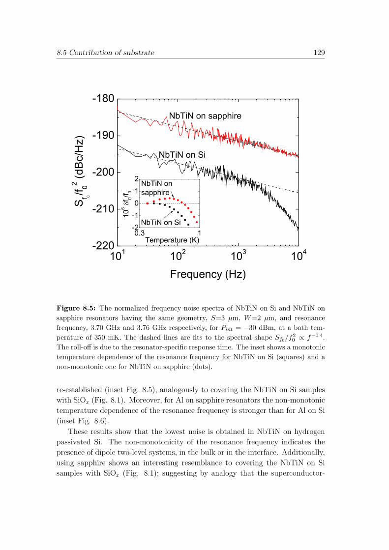
8.5 Contribution of substrate 129
101 102 103 104-220
-210
-200
-190
-180
0.3 1-2-1012
106
f 0/f 0
Temperature (K)
NbTiN on Si
NbTiN on sapphire
NbTiN on Si
NbTiN on sapphire
S
f 0/f 02 (dB
c/H
z)
Frequency (Hz)
Figure 8.5: The normalized frequency noise spectra of NbTiN on Si and NbTiN onsapphire resonators having the same geometry, S=3 µm, W=2 µm, and resonancefrequency, 3.70 GHz and 3.76 GHz respectively, for Pint = −30 dBm, at a bath tem-perature of 350 mK. The dashed lines are fits to the spectral shape Sf0/f2
0 ∝ f−0.4.The roll-off is due to the resonator-specific response time. The inset shows a monotonictemperature dependence of the resonance frequency for NbTiN on Si (squares) and anon-monotonic one for NbTiN on sapphire (dots).
re-established (inset Fig. 8.5), analogously to covering the NbTiN on Si samples
with SiOx (Fig. 8.1). Moreover, for Al on sapphire resonators the non-monotonic
temperature dependence of the resonance frequency is stronger than for Al on Si
(inset Fig. 8.6).
These results show that the lowest noise is obtained in NbTiN on hydrogen
passivated Si. The non-monotonicity of the resonance frequency indicates the
presence of dipole two-level systems, in the bulk or in the interface. Additionally,
using sapphire shows an interesting resemblance to covering the NbTiN on Si
samples with SiOx (Fig. 8.1); suggesting by analogy that the superconductor-
130 Chapter 8. Noise in NbTiN, Al and Ta superconducting resonators
101 102 103 104-205
-195
-185
-175
-165
0.1 0.3-2-1012
106
f 0/f 0
Temperature (K)
Al on sapphire
Al on Si
Al on sapphire
S
f 0/f 02 (dB
c/H
z)
Frequency (Hz)
Al on Si
Figure 8.6: The normalized frequency noise spectra of Al on Si and Al on sapphireresonators with equal geometry (S=3 µm, W=2 µm) and similar resonance frequency,4.22 GHz and 4.57 GHz respectively, for Pint = −40 dBm, at a bath temperature of100 mK. The dashed lines are fits to the spectral shape Sf0/f2
0 ∝ f−0.45. The roll-offis due to the resonator-specific response time. The inset shows a more pronouncednon-monotonicity in the temperature dependence of the resonance frequency for Al onsapphire (dots) compared to Al on Si (squares).
substrate interface contributes to the noise as well (in contrast to the assumption
by Bialczak et al. [18]). Most importantly, both the effect on the noise of a
dielectric layer on top in Fig. 8.1, and the change in substrate as shown in Figs.
8.5 and 8.6 strongly suggest that superconductor-dielectric interfaces contribute
to the frequency noise.
8.6 Discussion and conclusion 131
8.6 Discussion and conclusion
The identification of the source of the frequency noise is reminiscent of experi-
ments on the coherence for quantum information processing with superconduc-
tors. Josephson circuits exhibit a poorly understood 1/f flux noise. The source
of this flux noise is suggested to be related to spins at the surface. The physi-
cal mechanism has been conjectured to be due to spins of electrons in interface
defect states [19] or due to paramagnetic dangling bonds at interfaces [20]. In
this respect the hydrogen passivation of the Si is an important step in reducing
these contributions. Recently, the source of the flux noise has been suggested to
arise from RKKY (Ruderman-Kittel-Kasuya-Yosida) interactions between elec-
tron spins at interfaces of metals [21], supported by measurements on the mag-
netic properties of SQUIDs indicating the presence of surface spins on supercon-
ducting films [22]. In our resonators such interface spins would possibly couple
to the magnetic fields inside the resonator active region, appearing in the induc-
tance. Our data appear to be compatible with such a conceptual framework.
On the other hand, in recent work [23], connecting an interdigitated capacitor
to a transmission line resonator results in a reduction of the noise by 10 dB,
indicative of a strong contribution of a noise process located in dielectrics near
the superconductor.
To conclude, we find that the frequency noise in coplanar waveguide super-
conducting resonators and the deviations in the temperature dependence of the
resonance frequency are differently dependent on dielectrics, by measurements on
NbTiN on Si resonators with various coverages of SiOx. Additionally, the noise
can be decreased by increasing the width of the waveguide. The choice of sub-
strate is crucial for the level of noise, as we observe up to an order of magnitude
more noise in resonators comprised of NbTiN and Al on sapphire compared to Si.
The data indicate that the noise is strongly affected by superconductor-dielectric
interfaces. The source of the frequency noise in resonators, possibly being cor-
related to the flux noise in Josephson circuits which is associated with recently
observed surface spins, is a subject of future experimentation.
References
[1] P. K. Day, H. G. LeDuc, B. A. Mazin, A. Vayonakis and J. Zmuidzinas, A broad-band superconducting detector for use in large arrays, Nature 425, 817 (2003).
[2] A. Wallraff, D. I. Schuster, A. Blais, L. Frunzio, R. S. Huang, J. Majer, S. Ku-mar, S. M. Girvin and R. J. Schoelkopf, Strong coupling of a single photon to
132 Chapter 8. Noise in NbTiN, Al and Ta superconducting resonators
a superconducting qubit using circuit quantum electrodynamics, Nature 431, 162(2004).
[3] A. Palacios-Laloy, F. Nguyen, F. Mallet, P. Bertet, D. Vion, and D. Esteve, Tun-able resonators for quantum circuits, J. Low Temp. Phys. 151, 1034 (2008).
[4] R. Barends, J. J. A. Baselmans, S. J. C. Yates, J. R. Gao, J. N. Hovenier, and T.M. Klapwijk, Quasiparticle relaxation in optically excited high-Q superconductingresonators, Phys. Rev. Lett. 100, 257002 (2008).
[5] R. Barends, S. van Vliet, J. J. A. Baselmans, S. J. C. Yates, J. R. Gao, and T.M. Klapwijk, Enhancement of quasiparticle recombination in Ta and Al supercon-ductors by implantation of magnetic and nonmagnetic atoms, Phys. Rev. B 79,020509 (2009).
[6] J. J. A. Baselmans, S. J. C. Yates, R. Barends, Y. J. Y. Lankwarden, J. R. Gao,H. F. C. Hoevers, and T. M. Klapwijk, Noise and sensitivity of aluminum kineticinductance detectors for sub-mm astronomy, J. Low Temp. Phys. 151, 524 (2008);and unpublished results.
[7] J. Gao, J. Zmuidzinas, B. A. Mazin, H. G. LeDuc, and P. K. Day, Noise propertiesof superconducting coplanar waveguide microwave resonators, Appl. Phys. Lett.90, 102507 (2007).
[8] R. Barends, H. L. Hortensius, T. Zijlstra, J. J. A. Baselmans, S. J. C. Yates, J.R. Gao, and T. M. Klapwijk, Contribution of dielectrics to frequency and noise ofNbTiN superconducting resonators, Appl. Phys. Lett. 92, 223502 (2008).
[9] S. Kumar, J. Gao, J. Zmuidzinas, B. A. Mazin, H. G. LeDuc, and P. K. Day,Temperature dependence of the frequency and noise of superconducting coplanarwaveguide resonators, Appl. Phys. Lett. 92, 123503 (2008).
[10] J. Gao, M. Daal, A. Vayonakis, S. Kumar, J. Zmuidzinas, B. Sadoulet, B. A.Mazin, P. K. Day, and H. G. LeDuc, Experimental evidence for a surface distri-bution of two-level systems in superconducting lithographed microwave resonators,Appl. Phys. Lett. 92, 152505 (2008).
[11] J. Gao, M. Daal, J. M. Martinis, A. Vayonakis, J. Zmuidzinas, B. Sadoulet, B. A.Mazin, P. K. Day, and H. G. LeDuc, A semiempirical model for two-level systemnoise in superconducting microresonators, Appl. Phys. Lett. 92, 212504 (2008).
[12] W. A. Phillips, Two-level states in glasses, Rep. Prog. Phys. 50, 1657 (1987).
[13] R. L. Kautz, Picosecond pulses on superconducting striplines, J. Appl. Phys. 49,308 (1978).
[14] W. H. Henkels and C. J. Kircher, Penetration depth measurements on type IIsuperconductors, IEEE Trans. Magn. MAG-13, 63 (1977).
[15] M. Tinkham, Introduction to Superconductivity, (McGraw-Hill, New York, 1996).

References 133
[16] D.C. Mattis and J. Bardeen, Theory of the anomalous skin effect in normal andsuperconducting metals, Phys. Rev. 111, 412 (1958).
[17] J. C. Booth and C. L. Holloway, Conductor loss in superconducting planar struc-tures: calculations and measurements, IEEE Trans. Micr. Theory Tech. 47, 769(1999).
[18] R. C. Bialczak, R. McDermott, M. Ansmann, M. Hofheinz, N. Katz, E. Lucero,M. Neeley, A. D. OConnell, H. Wang, A. N. Cleland, and J. M. Martinis, 1/f Fluxnoise in josephson phase qubits, Phys. Rev. Lett. 99, 187006 (2007).
[19] R. H. Koch, D. P. DiVincenzo, and J. Clarke, Model for 1/f flux noise in SQUIDsand qubits, Phys. Rev. Lett. 98, 267003 (2007).
[20] R. de Sousa, Dangling-bond spin relaxation and magnetic 1/f noise from theamorphous-semiconductor/oxide interface: theory, Phys. Rev. B 76, 245306 (2007).
[21] L. Faoro and L. B. Ioffe, Microscopic origin of low-frequency flux noise in joseph-son circuits, Phys. Rev. Lett. 100, 227005 (2008).
[22] S. Sendelbach, D. Hover, A. Kittel, M. Muck, J. M. Martinis, and R. McDermott,Magnetism in SQUIDs at millikelvin temperatures, Phys. Rev. Lett. 100, 227006(2008).
[23] O. Noroozian, New resonator designs for reduced frequency noise in microwavekinetic inductance detectors, 2nd Workshop on the Physics and Applications ofSuperconducting Microresonators, SRON Utrecht, the Netherlands, 19-20 June,2008.
134 Chapter 8. Noise in NbTiN, Al and Ta superconducting resonators
Appendix A
Noise equivalent power
The noise equivalent power (NEP) is defined as the power per post-detection
bandwidth df = 1 Hz (integration time is 0.5 s) at the detector input with a
signal-to-noise ratio of one. In other words, the NEP is the incident power at the
input that doubles the output, i.e. adds an output signal level identical to the
output signal arising from the input noise.
Incident power P leads to an increase of the quasiparticle number
δNqp
δt=
ηP
∆− Nqp
τr
(A.1)
with η the absorption efficiency, ∆ the superconducting energy gap and τr the
recombination time. In the steady state, the above equation results in
Nqp =ητr
∆P (A.2)
Consequently, the response in the observable, the phase θ, is
< θ >=δθ
δNqp
< Nqp > (A.3)
Now we can write three identities for < θ2(f) >
< θ2(f) > = Sθ(f)df (A.4)
=( δθ
δNqp
)2 < N2qp(f) >
1 + (2πfτres)2=
( δθ
δNqp
)2 SNqp(f)df
1 + (2πfτres)2(A.5)
=( δθ
δNqp
)2(ητr
∆
)2 < P 2(f) >
[1 + (2πfτr)2][1 + (2πfτres)2](A.6)
The frequency-dependent part arises from the notion that the resonator (limited
by the resonator response time τres) cannot follow fast variations in the electron
system; additionally the electron system (characterised by the relaxation time τr)
135
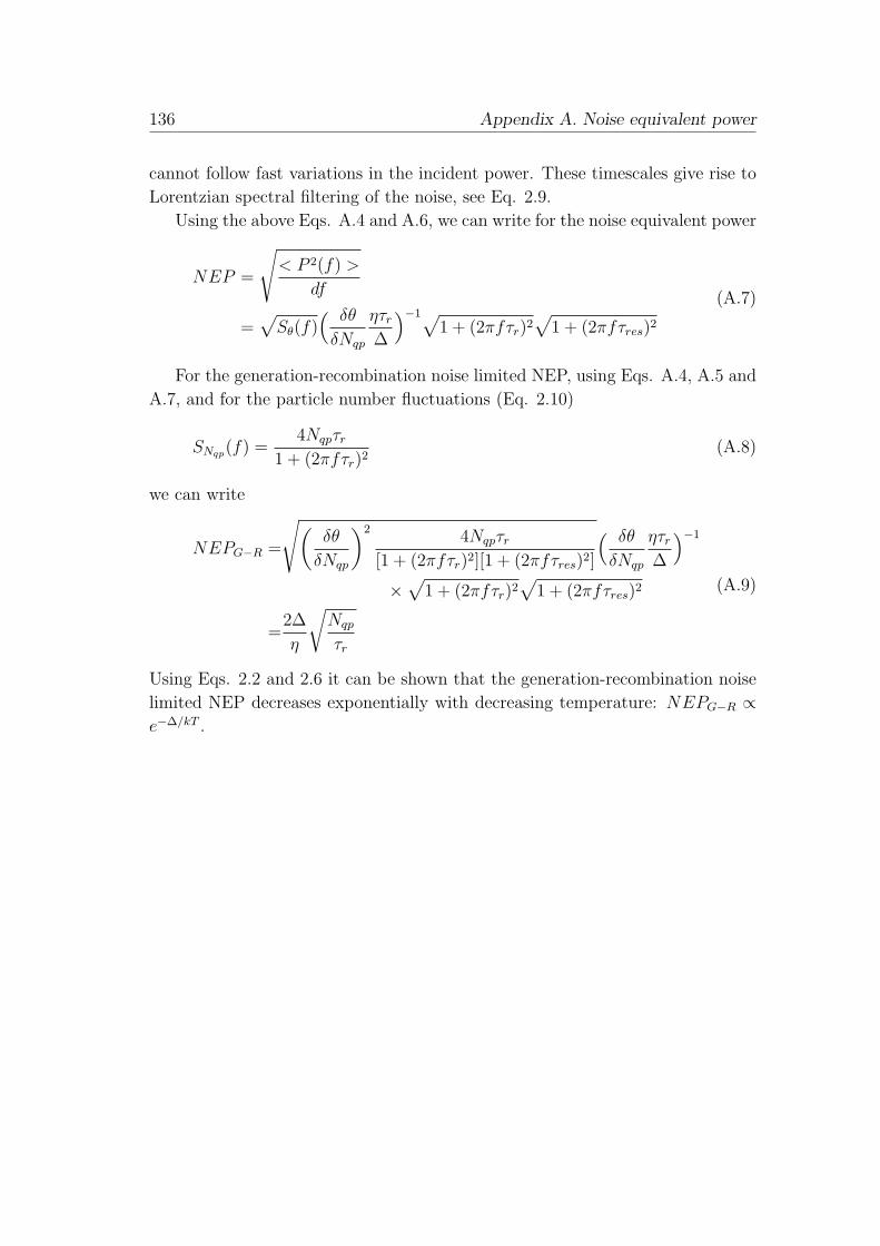
136 Appendix A. Noise equivalent power
cannot follow fast variations in the incident power. These timescales give rise to
Lorentzian spectral filtering of the noise, see Eq. 2.9.
Using the above Eqs. A.4 and A.6, we can write for the noise equivalent power
NEP =
√< P 2(f) >
df
=√
Sθ(f)( δθ
δNqp
ητr
∆
)−1√1 + (2πfτr)2
√1 + (2πfτres)2
(A.7)
For the generation-recombination noise limited NEP, using Eqs. A.4, A.5 and
A.7, and for the particle number fluctuations (Eq. 2.10)
SNqp(f) =4Nqpτr
1 + (2πfτr)2(A.8)
we can write
NEPG−R =
√(δθ
δNqp
)24Nqpτr
[1 + (2πfτr)2][1 + (2πfτres)2]
( δθ
δNqp
ητr
∆
)−1
×√
1 + (2πfτr)2√
1 + (2πfτres)2
=2∆
η
√Nqp
τr
(A.9)
Using Eqs. 2.2 and 2.6 it can be shown that the generation-recombination noise
limited NEP decreases exponentially with decreasing temperature: NEPG−R ∝e−∆/kT .
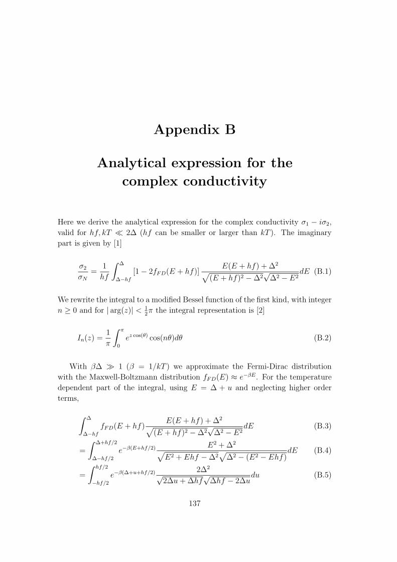
Appendix B
Analytical expression for the
complex conductivity
Here we derive the analytical expression for the complex conductivity σ1 − iσ2,
valid for hf, kT ¿ 2∆ (hf can be smaller or larger than kT ). The imaginary
part is given by [1]
σ2
σN
=1
hf
∫ ∆
∆−hf
[1− 2fFD(E + hf)]E(E + hf) + ∆2
√(E + hf)2 −∆2
√∆2 − E2
dE (B.1)
We rewrite the integral to a modified Bessel function of the first kind, with integer
n ≥ 0 and for | arg(z)| < 12π the integral representation is [2]
In(z) =1
π
∫ π
0
ez cos(θ) cos(nθ)dθ (B.2)
With β∆ À 1 (β = 1/kT ) we approximate the Fermi-Dirac distribution
with the Maxwell-Boltzmann distribution fFD(E) ≈ e−βE. For the temperature
dependent part of the integral, using E = ∆ + u and neglecting higher order
terms,
∫ ∆
∆−hf
fFD(E + hf)E(E + hf) + ∆2
√(E + hf)2 −∆2
√∆2 − E2
dE (B.3)
=
∫ ∆+hf/2
∆−hf/2
e−β(E+hf/2) E2 + ∆2
√E2 + Ehf −∆2
√∆2 − (E2 − Ehf)
dE (B.4)
=
∫ hf/2
−hf/2
e−β(∆+u+hf/2) 2∆2
√2∆u + ∆hf
√∆hf − 2∆u
du (B.5)
137
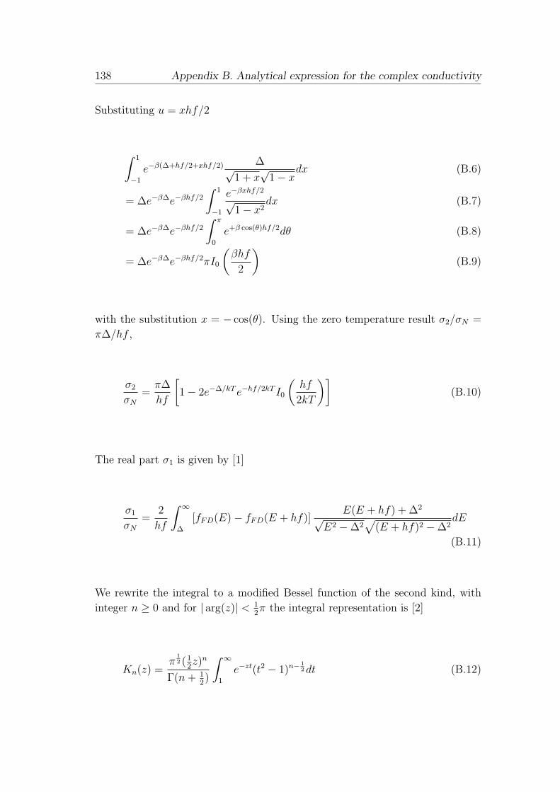
138 Appendix B. Analytical expression for the complex conductivity
Substituting u = xhf/2
∫ 1
−1
e−β(∆+hf/2+xhf/2) ∆√1 + x
√1− x
dx (B.6)
= ∆e−β∆e−βhf/2
∫ 1
−1
e−βxhf/2
√1− x2
dx (B.7)
= ∆e−β∆e−βhf/2
∫ π
0
e+β cos(θ)hf/2dθ (B.8)
= ∆e−β∆e−βhf/2πI0
(βhf
2
)(B.9)
with the substitution x = − cos(θ). Using the zero temperature result σ2/σN =
π∆/hf ,
σ2
σN
=π∆
hf
[1− 2e−∆/kT e−hf/2kT I0
(hf
2kT
)](B.10)
The real part σ1 is given by [1]
σ1
σN
=2
hf
∫ ∞
∆
[fFD(E)− fFD(E + hf)]E(E + hf) + ∆2
√E2 −∆2
√(E + hf)2 −∆2
dE
(B.11)
We rewrite the integral to a modified Bessel function of the second kind, with
integer n ≥ 0 and for | arg(z)| < 12π the integral representation is [2]
Kn(z) =π
12 (1
2z)n
Γ(n + 12)
∫ ∞
1
e−zt(t2 − 1)n− 12 dt (B.12)
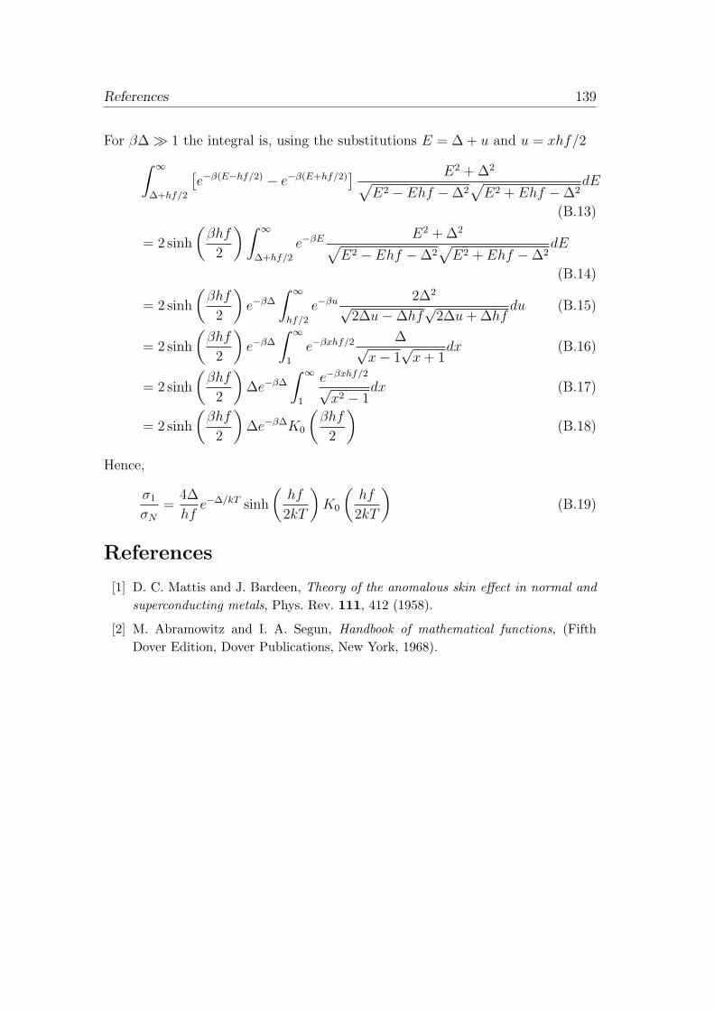
References 139
For β∆ À 1 the integral is, using the substitutions E = ∆ + u and u = xhf/2
∫ ∞
∆+hf/2
[e−β(E−hf/2) − e−β(E+hf/2)
] E2 + ∆2
√E2 − Ehf −∆2
√E2 + Ehf −∆2
dE
(B.13)
= 2 sinh
(βhf
2
) ∫ ∞
∆+hf/2
e−βE E2 + ∆2
√E2 − Ehf −∆2
√E2 + Ehf −∆2
dE
(B.14)
= 2 sinh
(βhf
2
)e−β∆
∫ ∞
hf/2
e−βu 2∆2
√2∆u−∆hf
√2∆u + ∆hf
du (B.15)
= 2 sinh
(βhf
2
)e−β∆
∫ ∞
1
e−βxhf/2 ∆√x− 1
√x + 1
dx (B.16)
= 2 sinh
(βhf
2
)∆e−β∆
∫ ∞
1
e−βxhf/2
√x2 − 1
dx (B.17)
= 2 sinh
(βhf
2
)∆e−β∆K0
(βhf
2
)(B.18)
Hence,
σ1
σN
=4∆
hfe−∆/kT sinh
(hf
2kT
)K0
(hf
2kT
)(B.19)
References
[1] D. C. Mattis and J. Bardeen, Theory of the anomalous skin effect in normal andsuperconducting metals, Phys. Rev. 111, 412 (1958).
[2] M. Abramowitz and I. A. Segun, Handbook of mathematical functions, (FifthDover Edition, Dover Publications, New York, 1968).
140 Appendix B. Analytical expression for the complex conductivity

Appendix C
Noise under continuous illumination
When shining light on a superconducting resonator, the resonance frequency
shifts and both the phase and amplitude noise levels increase. The shift in fre-
quency is due to the change in Cooper pair and quasiparticle density. Using Eq.
A.1, the amount of excess quasiparticles created by the incident light in the low
power limit (when the recombination time does not depend on the photo-excited
quasiparticle density) is given by
Nqp =Pτ
∆(C.1)
with P the absorbed power and τ the recombination time. The noise increase
reflects the photon shot noise. Analogous to electron shot noise, the relative
photon shot noise is given by
SP =2~ΩP
(C.2)
with dimension 1/Hz.
The frequency shift is proportional to the amount of excited quasiparticles,
hence: ∆f ∝ P . Therefore, the frequency power spectral density is proportional
to the noise in the power. As a result,
Sf0
f 20
=(∆f
f0
)2
SP (C.3)
The frequency noise is converted to the phase noise, using Eq. 3.24: Sθ =
(4Ql)2Sf0/f
20 .
In order to estimate the phase noise level under continuous optical illumi-
nation in the experiment described in Chapter 5 the responsivity and absorbed
power need to be determined. These are extracted from the resonance frequency
shift with temperature of the Ta resonator. The resonance frequency is plotted
141
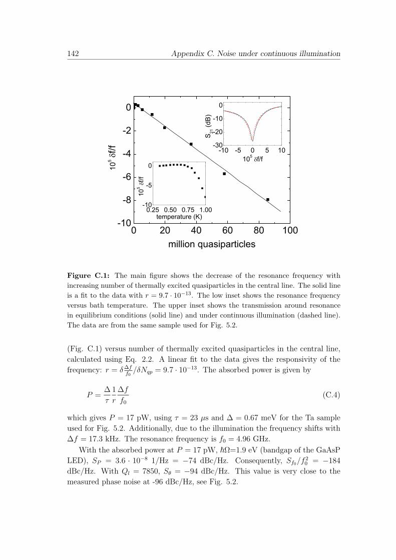
142 Appendix C. Noise under continuous illumination
0 20 40 60 80 100-10
-8
-6
-4
-2
0
-10 -5 0 5 10-30
-20
-10
0
S21
(dB
)
105 f/f
0.25 0.50 0.75 1.00-10
-5
0
105
f/f
temperature (K)
105
f/f
million quasiparticles
Figure C.1: The main figure shows the decrease of the resonance frequency withincreasing number of thermally excited quasiparticles in the central line. The solid lineis a fit to the data with r = 9.7 · 10−13. The low inset shows the resonance frequencyversus bath temperature. The upper inset shows the transmission around resonancein equilibrium conditions (solid line) and under continuous illumination (dashed line).The data are from the same sample used for Fig. 5.2.
(Fig. C.1) versus number of thermally excited quasiparticles in the central line,
calculated using Eq. 2.2. A linear fit to the data gives the responsivity of the
frequency: r = δ∆ff0
/δNqp = 9.7 · 10−13. The absorbed power is given by
P =∆
τ
1
r
∆f
f0
(C.4)
which gives P = 17 pW, using τ = 23 µs and ∆ = 0.67 meV for the Ta sample
used for Fig. 5.2. Additionally, due to the illumination the frequency shifts with
∆f = 17.3 kHz. The resonance frequency is f0 = 4.96 GHz.
With the absorbed power at P = 17 pW, ~Ω=1.9 eV (bandgap of the GaAsP
LED), SP = 3.6 · 10−8 1/Hz = −74 dBc/Hz. Consequently, Sf0/f20 = −184
dBc/Hz. With Ql = 7850, Sθ = −94 dBc/Hz. This value is very close to the
measured phase noise at -96 dBc/Hz, see Fig. 5.2.
Noise under continuous illumination 143
This noise level exceeds the quasiparticle generation-recombination noise.
From Eq. 2.6 we expect the value of Nτ = 1.9 · 102 (using τ0 = 42 ns and
2Na(0) = 4.3 · 1047 1/Jm3). Hence, Eq. 2.10 gives SN = 7.4 · 102 1/Hz, leading
to Sf0/f20 = r2SN = −210 dBc/Hz, which is far below the frequency noise arising
from the photon shot noise.
144 Appendix C. Noise under continuous illumination
Summary
Photon-detecting superconducting resonators
One of the greatest challenges in astronomy is observing the universe in the far-
infrared with large imaging arrays (100x100 pixels or more) with a sensitivity so
high, that it is limited by the background emanations of the universe itself. Su-
perconducting resonators are ideally suited for this task. In superconductors, the
electrons are paired with a binding energy small enough for far-infrared photons
to create unpaired excitations, or quasiparticles. These devices can be operated
at temperatures where less than a billionth of the electrons are thermally ex-
cited, sensitively probing the photo-excited particles. At the same time, these
resonators have quality factors reaching values on the order of a million, and
are able to sense tiny variations. By giving each resonator (or pixel) a slightly
different length, like the pipes in an organ, many can be read out simultaneously
in the frequency domain. This frequency domain multiplexing allows for the
construction of large imaging arrays.
Photon detectors work best when relaxation is slow. The steady stream of
incoming photons breaks many paired electrons into quasiparticle excitations.
The amount of excitations created, and consequently the detector sensitivity, is
proportional to the relaxation time. The relaxation occurs by the pairing, or
recombination, of these quasiparticle excitations into the paired particles, which
bring about the characteristic superconducting properties such as the complex
conductivity and, by extension, the kinetic inductance. As the detection mech-
anism essentially relies on counting paired electrons and unpaired excitations,
particle number fluctuations are a fundamental noise limit. Additionally, possi-
bly present dipoles and magnetic spins can couple to the electric and magnetic
fields in the resonator, giving rise to noise.
Interestingly, the drive for sensitive detectors for observing the universe boils
down to fundamental questions about the microscopic processes: “How do elec-
trons interact and exchange energy?”, and “What fluctuates at low temperatures,
causing noise?”. These questions lie at the heart of mesoscopic physics. This the-
sis describes a series of experiments aimed at elucidating the physical mechanisms
145
146 Summary
behind these processes.
We start with our experiments by first measuring the low temperature prop-
erties of superconducting resonators. In principle these properties are controlled
by the superconductor, but for Nb and Ta, we find that with decreasing tempera-
ture the quality factor increases exponentially, yet saturates at low temperatures.
Additionally, a clear nonmonotonicity in temperature dependence of the reso-
nance frequency is observed at low temperatures. These observations signal the
presence of additional processes influencing resonator properties. Preliminary
measurements of the noise indicate a considerable low frequency contribution
coming from the resonator itself. Having tested our designs we shift our focus to
quasiparticle relaxation.
Using superconducting resonators we, for the first time, directly probe the
low temperature quasiparticle recombination processes using the response of the
complex conductivity to photon flux. For both Ta and Al we find that at high
temperatures the relaxation times increase with decreasing temperature, as ex-
pected for recombination with electron-phonon interaction. At low temperatures
we find relaxation times as long as a millisecond for Al and several tens of mi-
croseconds for Ta. Moreover, we find a clear saturation of the relaxation times
at low temperatures in both materials, indicating the presence of an additional
recombination channel in the superconducting films. Motivated by reminiscence
of the low temperature saturation to experiments in normal metals on inelastic
scattering among electrons, we investigate the influence of magnetic impurities on
the recombination process. We find that low temperature relaxation is strongly
enhanced by the implantation of magnetic as well as nonmagnetic atoms, while
the relaxation at high temperatures is only weakly affected. This indicates that
the enhancement of low temperature recombination arises from an enhancement
of disorder.
In the remaining part we turn to the subject of excess frequency noise and
deviations in the temperature dependence of the resonance frequency, which have
been widely observed at low temperatures. We have found that NbTiN, on hy-
drogen passivated Si, does not show a nonmonotonic temperature dependence
of the resonance frequency. We show that this temperature dependence is re-
established by covering the samples with sputtered thin SiOx layers, and that
these deviations scale with the thickness. In addition, we find that the frequency
noise is strongly increased as soon as a SiOx layer is present; but is, in contrast,
independent of the layer thickness. This indicates that the noise is dominantly
due to processes occurring at interfaces, whereas deviations in the temperature
dependence arise from processes in the volume of the dielectric. Finally, we find
that we can significantly decrease the noise by widening the geometry of the res-

147
onator waveguide, and that the noise is lowest when using hydrogen passivated
Si instead of sapphire as substrate.
Rami Barends
Delft, April 2009

148 Summary
Samenvatting
Foton-detecterende supergeleidende resonatoren
Een van de grootste uitdagingen in de astronomie is het waarnemen van het
universum in het ver-infrarood met een grote camera (meer dan 100x100 beeld-
punten) die een gevoeligheid heeft die zo hoog is dat de achtergrondstraling van
het universum zelf de limiterende factor is. Supergeleidende resonatoren zijn
uitermate geschikt voor deze taak. In supergeleiders zijn de elektronen gepaard
met een bindingsenergie die zo klein is dat ver-infrarood fotonen paren kunnen
opbreken en ongepaarde excitaties kunnen creeren, zogenaamde quasideeltjes.
Deze resonatoren worden gebruikt op temperaturen waar minder dan een mil-
jardste van de elektronen thermisch geexciteerd zijn, derhalve kunnen deeltjes
die door fotonen zijn geexciteerd gevoelig opgemerkt worden. Anderszijds kan
de kwaliteitsfactor van deze resonatoren oplopen tot wel een miljoen; hierdoor
kunnen hele kleine veranderingen gevoeld worden. Door iedere resonator (of
beeldpunt) een iets andere lengte te geven, net zoals bij orgelpijpen, kunnen ve-
len tegelijkertijd uitgelezen worden in het frequentiedomein. Dit multiplexen in
het frequentiedomein staat de bouw van grote camera’s toe.
Fotondetectoren werken het beste wanneer relaxatie langzaam plaatsvindt. De
stroom aan inkomende fotonen creeert vele ongepaarde excitaties. De hoeveelheid
excitaties, en daarmee de gevoeligheid van de detector, is evenreding met de
relaxatietijd. Relaxatie vindt plaats door het paren, oftewel de recombinatie, van
ongepaarde quasideeltjes tot gepaarde elektronen, deze brengen de karakteristieke
eigenschappen van supergeleiders voort zoals de complexe geleiding en daarmee
de kinetische zelfinductie.
Interessant genoeg komt de ontwikkeling van gevoelige detectoren om het
universum waar te nemen neer op het beantwoorden van fundamentele vragen
over microscopische processen: “Hoe vindt de interactie tussen elektronen plaats
en wordt energie uitgewisseld?”, en “Wat fluctueert op lage temperaturen en
genereert ruis?”. Deze vragen liggen aan de basis van de mesoscopische fysica.
Dit proefschrift beschrijft een set van experimenten opgezet om de fysische mecha-
nismen achter deze processen te ontrafelen.
149
150 Samenvatting
We beginnen met de experimenten door de eigenschappen van supergeleidende
resonatoren op lage temperaturen te meten. In principe worden deze voortge-
bracht door de supergeleider, maar voor de materialen Nb en Ta zien we dat
met lager wordende temperatuur de kwaliteitsfactor eerst exponentieel toeneemt
en dan gek genoeg satureert op lage tempeturen. Ook is er duidelijk een niet-
monotone temperatuur afhankelijkheid te zien in de resonantiefrequentie op lage
temperaturen. Deze waarnemingen geven aan dat er meerdere processen zijn die
de eigenschappen van resonatoren beınvloeden. Eerste ruismetingen laten ook
zien dat een behoorlijke hoeveelheid ruis uit de resonatoren zelf komt. Nu we het
ontwerp van de resonatoren getest hebben concentreren we ons op de relaxatie
van quasideeltjes.
Met supergeleidende resonatoren observeren we, voor het eerst, direct de re-
combinatie van quasideeltjes op lage temperaturen door gebruik te maken van
de respons van de complexe geleiding op een fotonenstroom. Voor Ta en Al vin-
den we dat op hoge temperaturen de relaxatietijden omhoog gaan wanneer de
temperatuur verlaagd wordt, zoals verwacht voor recombinatie met overdracht
van de energie naar het kristalrooster. Op lage temperaturen vinden we relax-
atietijden van bijna een milliseconde voor Al en tientallen microseconden voor
Ta. Eveneens vinden we een duidelijke saturatie van de relaxatietijden op lage
temperaturen in beide materialen, dit duidt op de aanwezigheid van een tweede
recombinatieproces in de supergeleidende films. Deze saturatie doet denken aan
experimenten aan inelastische interactietijden in normale metalen. Met dit in het
achterhoofd, onderzoeken we de invloeden van magnetische verontreinigingen op
het recombinatieproces. We vinden dat op lage temperaturen de relaxatie flink
sterker is geworden door de implantatie van magnetische alsook niet-magnetische
atomen. Dit terwijl de relaxatie op hogere temperaturen nauwelijks beınvloed
wordt. Deze resultaten geven aan dat een versterking van het recombinatiepro-
ces op lage temperaturen veroorzaakt wordt door een versterking van wanorde.
Vervolgens richten we ons op de behoorlijke hoeveelheid frequentieruis en de
afwijkingen in de temperatuurafhankelijkheid van de resonantiefrequentie, deze
zijn op grote schaal gesignaleerd op lage temperaturen. We vinden dat NbTiN op
Si, dat gepassiveerd is met waterstof, geen niet-monotone temperatuurafhanke-
lijkheid van de resonantiefrequentie vertoont. We laten zien dat deze temper-
atuurafhankelijkheid terugkomt als we de resonatoren bedekken met een dunne
dielektrische laag SiOx, en dat deze afwijkingen schalen met de dikte van de laag.
Daarentegen springt de frequentieruis omhoog zodra een SiOx laag aanwezig is,
maar stijgt niet verder met dikkere lagen. Dit laat zien dat de ruis voornamelijk
komt door processen aan oppervlakken, terwijl afwijkingen in de temperatuu-
rafhankelijkheid van de resonantiefrequentie voortkomen uit processen in het
151
volume van de dielektrische laag. Tenslotte vinden we dat we de ruis signifi-
cant kunnen verminderen door een bredere geometrie voor de transmissielijn van
de resonator te kiezen en dat de ruis het laagst is wanneer met waterstof gepas-
siveerd Si wordt gebruikt als substraat.
Rami Barends
Delft, april 2009

152 Samenvatting
Curriculum Vitae
Rami Barends
6 May 1981 Born in Delft, The Netherlands.
1993-1999 Grammar school
Grotius College, Delft
1999-2004 M. Sc. in Applied Physics (cum laude)
Delft University of Technology
Graduate research in the group of prof. dr. ir. T. M. Klapwijk
Subject: Analysing Superconducting THz Detectors:
Non-equilibrium Double Barrier Junctions
and Hot Electron Bolometer Mixers
Received scholarship “Sterbeurs”
for highly promising first year students (1999)
Received “Study Prize Applied Physics”
for outstanding graduation research (2004)
2004-2009 Ph. D. research at Delft University of Technology
Subject: Photon-detecting superconducting resonators
Promotor: Prof. dr. ir. T. M. Klapwijk
Copromotor: Dr. J. R. Gao
153

154
List of publications
1. R. Barends, H. L. Hortensius, T. Zijlstra, J. J. A. Baselmans, S. J. C. Yates,J. R. Gao, and T. M. KlapwijkNoise in NbTiN, Al and Ta superconducting resonators on silicon and sapphiresubstratesaccepted for publication in IEEE Transactions on Applied Superconductivity(2009).
2. R. Barends, S. van Vliet, J. J. A. Baselmans, S. J. C. Yates, J. R. Gao, andT. M. KlapwijkQuasiparticle relaxation in high Q superconducting resonatorsJournal of Physics: Conference Series 150, 052016 (2009).
3. R. Barends, S. van Vliet, J. J. A. Baselmans, S. J. C. Yates, J. R. Gao, andT. M. KlapwijkEnhancement of quasiparticle recombination in Ta and Al superconductors byimplantation of magnetic and nonmagnetic atomsPhysical Review B 79, 020509(R) (2009).
4. R. Barends, J. J. A. Baselmans, S. J. C. Yates, J. R. Gao, J. N. Hovenier, andT. M. KlapwijkQuasiparticle relaxation in optically excited high-Q superconducting resonatorsPhysical Review Letters 100, 257002 (2008).
5. R. Barends, H. L. Hortensius, T. Zijlstra, J. J. A. Baselmans, S. J. C. Yates,J. R. Gao, and T. M. KlapwijkContribution of dielectrics to frequency and noise of NbTiN superconducting res-onatorsApplied Physics Letters 92, 223502 (2008).
6. R. Barends, J. J. A. Baselmans, S. J. C. Yates, J. N. Hovenier, J. R. Gao, andT. M. KlapwijkQuasiparticle lifetime and noise in tantalum high Q resonators for kinetic induc-tance detectorsJournal of Low Temperature Physics 151, 518 (2008).
155

156 List of publications
7. J. J. A. Baselmans, S. J. C. Yates, R. Barends, J. J. Lankwarden, J. R. Gao,H. Hoevers, and T. M. KlapwijkNoise and sensitivity of aluminum kinetic inductance detectors for sub-mm as-tronomyJournal of Low Temperature Physics 151, 524 (2008).
8. J. J. A. Baselmans, S. J. C. Yates, P. de Korte, H. F. C. Hoevers, R. Barends,J. N. Hovenier, J. R. Gao, and T. M. KlapwijkDevelopment of high-Q superconducting resonators for use as kinetic inductancedetectorsAdvances in Space Research 40, 708 (2007).
9. J. R. Gao, M. Hajenius, Z. Q. Yang, J. J. A. Baselmans, P. Khosropanah,R. Barends, and T. M. KlapwijkTerahertz Superconducting Hot Electron Bolometer Heterodyne ReceiversIEEE Transactions on Applied Superconductivity 17, 252 (2007).
10. R. Barends, J. J. A. Baselmans, J. N. Hovenier, J. R. Gao, S. J. C. Yates,T. M. Klapwijk, and H. F. C. HoeversNiobium and tantalum high Q resonators for photon detectorsIEEE Transactions on Applied Superconductivity 17, 263 (2007).
11. D. Loudkov, R. Barends, M. Hajenius, J. R. Gao, and T. M. KlapwijkResistivity of Ultrathin Superconducting NbN Films for Bolometer MixersIEEE Transactions on Applied Superconductivity 17, 387 (2007).
12. R. Barends, J. N. Hovenier, J. R. Gao, T. M. Klapwijk, J. J. A. Baselmans,S. J. C. Yates, Y. J. Y. Lankwarden, and H. F. C. HoeversQuasiparticle lifetime in tantalum kinetic inductance detectorsProceedings of the 18th International Symposium on Space Terahertz Technol-ogy, Caltech, Pasadena, USA, p. 180, 21-23 March 2007.
13. J. J. A. Baselmans, R. Barends, J. N. Hovenier, J. R. Gao, H. F. C. Hoevers,and T. M. KlapwijkDevelopment of high-Q superconducting resonators for use as kinetic inductancesensing elementsNuclear Instruments and Methods in Physics Research Section A 559, 567 (2006).
14. R. Barends, M. Hajenius, J. R. Gao, and T. M. KlapwijkCurrent-induced vortex unbinding in bolometer mixersApplied Physics Letters 87, 263506 (2005).
15. M. Hajenius, R. Barends, J. R. Gao, T. M. Klapwijk, J. J. A. Baselmans,A. Baryshev, B. Voronov, and G. Gol’tsmanLocal resistivity and the current-voltage characteristics of hot electron bolometer
157
mixersIEEE Transactions on Applied Superconductivity 15, 495 (2005).
16. R. Barends, M. Hajenius, J. R. Gao and T. M. KlapwijkDirect correspondence between HEB current-voltage characteristics and the current-dependent resistive transition, Proceedings of the 16th International Symposiumon Space Terahertz Technology, Goteborg, Sweden, p. 416, 2-4 May 2005.
17. T. M. Klapwijk, R. Barends, J. R. Gao, M. Hajenius, and J. J. A. BaselmansImproved superconducting hot-electron bolometer devices for the THz rangeProceedings of the Society of Photo-optical Instrumentation Engineers (SPIE)5498, 129 (2004).
18. R. Barends, J. R. Gao and T. M. KlapwijkHot Electron Superconducting Detector using a Double Barrier JunctionProceedings of the 6th International Workshop on Low Temperature Electronics(WOLTE-6), ESTEC Noordwijk, p. 25, 23-25 June 2004.
158 List of publications
The thought had crossed my mind
“The thought had crossed my mind” was the cryptic answer Teun got when he
asked me whether I already thought of doing a PhD in his group. At the time I was
halfway through the final year, yet nearly finished with the subject of nonequilib-
rium double barrier junctions; I was however not convinced my master’s, guided
by Gao, was complete. Therefore we turned to hot electron bolometers for the re-
mainder, which resulted in a publication in Applied Physics Letters later on. My
master’s awoke the appetite for understanding physical processes, for identifying
their role in measurable quantities and for contributing to the beautiful symbiosis
between physics occurring at the nanoscale and astronomical instrumentation for
observing the universe.
After my internship in Cologne, where I was introduced to high frequency
measurements, I was ready to take on a new challenge with photon-detecting
superconducting resonators, in close collaboration with Jochem in Utrecht. This
was not only a highly promising concept, but also a new direction for detection,
a new way of probing physics at low temperatures as well as an experimentally
challenging subject: at the start there was not a single SMA connector in our
lab. The ramifications of the thought that crossed my mind culminated in the
thesis you now hold in your hands.
Though obtaining a PhD degree is an individual achievement, the path to-
wards it is nonetheless a team effort. Teun, it has been a pleasure to work, a
learning experience to write articles, and a privilege to have so many enthusiastic
discussions with you. You would always make the time to critically discuss any
kind of issue. Your ability to quickly switch topics and address the physics be-
neath is inspiring. In addition, your ‘Teunisms’ and witty remarks have enriched
my vocabulary! Gao, thanks for all the sharp advices, your keenness and all the
support you gave, especially at the start. Your way of thinking and testing ideas,
whether designs or proposed series of samples, is praiseworthy. Also your com-
pany on so many conferences, workshops and visits was very pleasurable. Jochem,
the enthusiastic discussions, the help, the critical thinking and the cunning in-
sight have all been so helpful. While we were a city apart, we really work well
159

160 The thought had crossed my mind
together, whether on recombination experiments, samples, or quadrature mixers,
as if there is no distance. The phoning and mailing on a daily basis evidence
that there is a very close collaboration; which also became the running joke dur-
ing the KID workshop. I think we showed that you can do fundamental physics
and work towards directly improving the sensitivity of detectors at the same time
and that real improvements are obtained when these go hand-in-hand! Steve, you
really strengthened the KID team, being thoroughly involved in the discussions
and experiments. Thanks also for the occasional lessons in upper-class British
English!
Yet experiments cannot be carried out so successfully without the technicians.
Niels, thanks for all the help with building the setup and with the experiments.
You really taught me a lot about RF, especially about mismatches! In addition to
cooling cryostats with liquid nitrogen and helium when needed, you also took care
we did not dry up, whether it was with alcohol or tea: you exposed us to all to a
whole brave new world of tea, especially the chrysanthemum tea which turned out
to be non-vegetarian! Tony, thanks for all the samples you made and for keeping
a down-to-earth approach to sample fabrication, your calmness is something to
envy! Mascha, you’ve been a very supportive Bond-girl! Additionally, a big
thanks goes out to Aad for doing a lot of machining for the cryostat, to Raymond
for lending so many items and to all the guys at the instrumentendienst for helping
out with the cryostat wiring.
But wait, the ramifications don’t stop here! Merlijn, you’ve been one of the
most interesting people I’ve met, encouraging me already during my bachelor
project all the way to the ‘knetterdetetters’. You keep to amaze me, whether it is
with food ranging from peanut butter to cryogenic apples, to near-misses in the
cleanroom with exploding dragonflies, or hilarious moments like boating trips in
Sweden (did you find a decent restaurant after you missed the boat?). About
the cleanroom, you should ‘hang’ you-know-who with the blue headgear on a
prominent place! Moreover, we have shared all the ups and downs, the hotspots
and cryo-leaks, concluding during one of the many evening dinners that we work
with cryostats. And yes, I might feel a little resentment over freezing your hair,
but only a tiny bit. Thanks for everything!
Of course, roommates are an intricate part to PhD. Chris, thanks for being my
roommate for so long and for all the conference visits we did together. Whether
it was the trip to Sweden, getting lost in Seattle, venturing into the desert in
California or taking it easy in Chicago, we always turned it into a little holiday. I
feel privileged for being your “rock in the burning”, whether in our room or during
that famous ‘Picnic’-moment on the German motorway. Let’s keep these good
memories, also from Oktoberfest (luckily we’ve got the pictures)! By the way,
161
are you already developing an appetite for Knoedels? Gabri, thanks for being my
roommate, for the lunch-applause and for keeping the focus on “klemmen!”. In
the too short time you were with us we really took over each other’s best traits.
Akira, apart from becoming my roommate you will also now further ‘father’ the
KIDs. Good luck to you, and it is great to see you pick up so quickly.
In addition, I had the honour of supervising many students. Rik, it has been
a pleasure to work with you and see you grow. You have become happy with
the bonding machine and lots of experimental work and measurements (‘houtje-
touwtje-knutsel-avontuurtje’), culminating in you being co-author of a publica-
tion. Obviously I didn’t scare you enough as you are now doing a PhD in our
group. And now you live with the credo “see the data, feel the data, be the data”!
I have confidence that you grow both financially as well as intellectually, so we
can rightfully call you “Rikkefeller”. Jeroen, we kept it cool when things were
over or under pressure. Simon, you have been a great help. I sometimes forgot it
was only a bachelor’s project, yet you really contributed towards a publication!
Do you still dream of bonding? Pieter, thanks for all the help and it is great to
see you came back for more! Werner, you are becoming more practical everyday,
and thanks for the conversations about finance (Middelkoop!).
I would also like to thank the guys at SRON for discussions, samples and
nice dinners during conferences: Henk Hoevers, Jan-Joost Lankwarden (thanks
for all the fabrication!), Andrey Baryshev, Pourya Khosropanah (“I’ll find me a
beggar”, holding a bag with chicken after Gao got more than he bargained for)
and Piet de Korte.
I would like to thank Yuli Nazarov, Yaroslav Blanter and Tero Heikkila for
the scientific discussions. In addition, the discussions with the ESTEC group -
Richard Hijmering, Peter Verhoeve, Alexander Kozorezov and Alexander Golubov
- were really helpful. Pleasurable and constructive interactions during the many
visits and conferences were also with the group at Caltech/JPL - Jonas Zmuidzinas,
Peter Day, Ben Mazin, Jiansong Gao, Megan Eckart and Shwetank Kumar - as
well as with the Cardiff group - Phil Mauskopf and Simon Doyle.
I also want to thank all the others which are or have been part of our group.
Nathan, thanks for the social events and many conversations, for helping to
redefine the anatomy of man (can you already reach your kikularis?), and for
slowly picking up the hard g. Gratefully, you are becoming encouragingly more
dutchable. Mr. Alibey, thanks for the many hilarious discussions in English
(remember: the tree is outside) and the social events, one during which you
exclaimed “I went to the shop, but the shop wasn’t there”. I hope your naviga-
tional skills (“Alibey, Alibey, Alibey, always the wrong way”) improve over time.
Moreover, I had a great time with Tarun (we might still get you that drinking
162 The thought had crossed my mind
licence!), Saverio (you still owe me the recipe for lasagna in the Nordiko), to-
varishch Dennis, Ruurd (how’s your stomach?), Frank (roommie!), Alberto (I
miss the discussions on Italian politics), Shaojiang, Yuan, Remco (if all else fails,
we could start the ‘Pleurop’ company!), Matthias, Omid (thanks for existential
discussions on bananas), Elfi (any more candy?), Tim, Amar and all the BSc
students. Outside of our group, I had an enjoyable interaction with Pol (thanks
for the Spanish), Thomas, Anna, Monica, Benoit, Christian, Jeroen, and a spe-
cial thanks goes to my ‘zwarte pieten’ Edgar and Menno. Also we had frequent
guests: Franzie (cleaning ist spaß!), Kate (“no beer, only vodka”). Moreover,
Ari and Pasi from Finland were a great help in the cleanroom during their very
fruitful ‘holiday’ month with us. Do you guys already have a huge yacht, and Ari,
do you need some more Delft Blue? And of course a big thanks goes out to the
secretaries Maria, Monique and Irma, not only for their assistance but also for
keeping the spirits high at the coffee table and for enforcing a tight dish washing
schedule.
Most importantly, I would like to thank my parents, brother and sister for
their unconditional support.
All this did not cross my mind more than four years ago, but it was a starting
point for a great experience. What a thought.
Rami Barends
Delft, April 2009


![COMPUTATIONAL 3D AND REFLECTIVITY IMAGING WITH HIGH PHOTON …akirmani/papers/ShinKGS_ICIP2014.pdf · be replaced with a superconducting nanowire single-photon detector (SNSPD) [18],](https://img.pdfslide.us/doc/110x75/5ec770430b24422ec45611e5/computational-3d-and-reflectivity-imaging-with-high-photon-akirmanipapersshinkgs.jpg)