Embed Size (px)
Citation preview
Photomask Technology 2015
Actinic Review of EUV Masks: Status and Recent Results of the AIMSTM EUV SystemSascha Perlitz and Jan Hendrik Peters, Carl Zeiss SMT GmbH, Carl-Zeiss-Promenade 10, 07745 Jena, Germany
Markus Weiss, Dirk Hellweg, Renzo Capelli, and Krister Magnusson, Carl Zeiss SMT GmbH, Rudolf-Eber-Str. 2, 73447 Oberkochen, Germany
Matt Malloy and Stefan Wurm, SUNY Poly SEMATECH, 257 Fuller Road, 12203 Albany, NY, US
ABSTRACT
Key enabler of the successful introduction of EUV lithography into volume production is the EUV mask infrastructure. For the production of defect free masks, actinic review of potential defect sites to decide on the need for repair or compensation is required. Also, the repair or compensa-tion with the ZEISS MERiT electron beam repair tool needs actinic verification in a closed loop mask repair solution. For the realization of actinic mask review, ZEISS and the SEMATECH EUVL Mask Infrastructure consortium started a development program for an EUV aerial image metrology system, the AIMS™ EUV, with realization of a prototype tool.
The development and prototype realization of the AIMS™ EUV has entered the tool calibration and qualification phase utilizing the achieved capabilities of EUV aerial image acquisition and EUV mask handling. In this paper, we discuss the current status of the prototype qualification and show recent measurement results.
1. Introduction
As EUV Lithography is intensively advancing towards its introduction into the semiconductor manu-facturing process, efforts are being made throughout industry to overcome the severe scientific and technological challenges that this paradigm change brings with it. Challenges have recently been advocated to be compelling for the realization of the full EUV infrastructure, among which EUV photomask defectivity is a top priority venture.
Regarding photomask defectivity qualification, the need for an actinic review and inspection tool is made necessary by the very nature of EUV light and its reflection process onto EUV optics. While for 193 nm lithography the class of defects can be fairly circumscribed to absorber defects
Figure 1. AIMS™ EUV prototype tool development path to final specification.
PhotomaskPhotomaskBACUS—The international technical group of SPIE dedicated to the advancement of photomask technology.
9635
-75
N • E • W • S
January 2016 Volume 32, Issue 1
Industry BrIefs—see page 8
CalendarFor a list of meetings —see page 9
Take A Look Inside:

EditorialIt’s All About TimeArtur Balasinski, Cypress Semiconductor, December 2015
As we enter the New Year 2016, we want to carry on with things that we do well and do away with things that bother us. What do we do well? Enable. Enabling speed to information and enabling speed to good times, are the first things that came to my mind. What bothers us? We are lazy. We want to put up a monumental job that would solve all the problems for us, but do it once and then - relax. Unfortunately, it is not that simple. It is about time to understand that our industry, just like many others, is providing a service. What is NOT providing a service? Food industry. We need to eat to survive. What else IS providing a service? Transportation industry, my favorite. Let’s look at what is happening there. Why? Because I believe that all service-oriented industries are similar and I want to explain the present to predict the future. And I can do this based on the experience of the industry that has been there already. Not long ago, it was believed that monumental constructions are the solution. Monumental buildings, monumental vessels, monumental fabs. Time is verifying this, case by case. Monumental buildings and monumental aircraft look awe-inspiring. Trouble is, they do not serve the general public, only the few ones who live near a big hub or want to take the time to get to one. It’s all about time. Much less monumental aircraft fly point to point and can fly more frequently, too. They provide better service, on the average. What else is providing better service? Custom IC’s. People may still need monstrous computers to predict the lifetime of the universe, but in the hoped-for-to-be era of Internet-of-Things or autonomous cars, we need small packs of diversified informa-tion rather than huge amounts of megapixels to be processed. Yes, we do need cost reduction per transistor, but cost reduction per seat only means more seats flying in the same direction. People care less and less about that. They would actually pay more for a direct flight, than for a two-legged flight, which would, in fact, still cost more to execute. The airlines know that already. In the IC and mask industry, we are still learning that 450 mm wafers and 7 nm MOSFETs can only take us this far. Yes, it is a monumental job to make this kind of technology happen, but it is not true that life would be so much easier once we reached that point. Many of these solutions would not shorten our time to information, in contrast, it may lengthen it. And it is all about time. What shortens our time to information? Working harder on custom solutions. A car ride cost more than a bus ride but somehow, most people prefer cars to buses. People who provide custom services faster would make better money, because it is all about time. So let’s go out there and make sure we can build more custom masks, faster. It is less monumental than 7 nm and not as much of a conversation piece, just like 100 tiny 737’s (or Neo’s if someone likes Airbuses) are less spectacular but still a big-ger deal than 10 huge A380’s (or 747’s, if someone is into Boeings). And they make more money and make more people happy. So let’s learn how to downsize on our legends but improve our service. It is all about time, and 2016 is a good time for us to understand it.
N • E • W • S
BACUS News is published monthly by SPIE for BACUS, the international technical group of SPIE dedicated to the advancement of photomask technology.
Managing Editor/Graphics Linda DeLano
Advertising Lara Miles
BACUS Technical Group Manager Pat Wight
■ 2016 BACUS Steering Committee ■
PresidentPaul W. Ackmann, GLOBALFOUNDRIES Inc.
Vice-PresidentJim N. Wiley, ASML US, Inc.
SecretaryLarry S. Zurbrick, Keysight Technologies, Inc.
Newsletter Editor Artur Balasinski, Cypress Semiconductor Corp.
2016 Annual Photomask Conference ChairsBryan S. Kasprowicz, Photronics, Inc.
Peter Buck, Mentor Graphics Corp
International Chair Uwe F. W. Behringer, UBC Microelectronics
Education ChairArtur Balasinski, Cypress Semiconductor Corp.
Members at LargeFrank E. Abboud, Intel Corp.
Paul C. Allen, Toppan Photomasks, Inc.Michael D. Archuletta, RAVE LLC
Peter D. Buck, Mentor Graphics Corp. Brian Cha, Samsung
Derren Dunn, IBM Albany Nanotechnology Lab.Thomas B. Faure, GLOBALFOUNDRIES Inc.
Brian J. Grenon, Grenon Consulting Jon Haines, Micron Technology Inc.
Naoya Hayashi, Dai Nippon Printing Co., Ltd.Mark T. Jee, HOYA Corp, USA
Patrick M. Martin, Applied Materials, Inc.M. Warren Montgomery, SUNY, The College of
Nanoscale Science and EngineeringShane R. Palmer, Nikon Research Corp. of America
Jan Hendrik Peters, Carl Zeiss SMS GmbH Michael T. Postek,
National Institute of Standards and TechnologyAbbas Rastegar, SEMATECH North
Douglas J. Resnick, Canon Nanotechnologies, Inc. Thomas Struck, Infineon Technologies AG
Bala Thumma, Synopsys, Inc.Michael Watt, Shin-Etsu MicroSi, Inc.
Mark Wylie, KLA-Tencor Corp.
P.O. Box 10, Bellingham, WA 98227-0010 USATel: +1 360 676 3290Fax: +1 360 647 1445
©2016
All rights reserved.

on top of the refracting glass substrate, EUV lithography extends the defect diversity, since the structure of the reflective multilayer mirror and the substrate can also strongly affect defect printabil-ity.1,2 As a result, only EUV actinic imaging can univocally deter-mine defect printability: AIMS™ EUV responds to this compelling necessity, completely fulfilling industry requirements in terms of performance specifications and scanner matching.3 The develop-ment of an actinic AIMS™ EUV system has been enabled by a collaboration between SEMATECH, ZEISS and the EMI consortium. Since more than twenty years the AIMS™ systems have served as crucial tools for mask shops for defect disposition and repair verification, having the great advantage of emulating the scanner mask illumination conditions.
In this work we report on the status of the AIMS™ EUV system development, focusing our discussion on the different development phases and on the fundamental tool capabilities that have been achieved and are already available for use on the tool. In section 2 the status of the prototype tool and of the first three customer tools is presented, followed by an update on the tool capability status (e.g. mask handling, image acquisition). Next, the current productivity (i.e. run rate) and performance (e.g. CD reproducibility and tool internal metrology reproducibility) status will be discussed, with the focus on the actual results which have been achieved on the prototype tool during the first measurement campaigns after the tool launch.
2. Project Status
The AIMS™ EUV project was started in the first half of 2011. In 2013 the completion of the hardware integration of the EUV Metrol-
ogy Core was achieved, which lead to the first important milestone of First Light in December 2013, in which the first EUV aerial images were measured. This milestone was a great achievement in terms of risk reduction and technology demonstration, and gave the go for the further integration of the entire system, accomplished in the last quarter of 2014. Since then, effort and focus has been devoted towards bringing the tool into operation. Figure 1 shows the time sequence of recent development steps carried out on the prototype tool: after final integration was achieved and first measurements with hardware completely assembled delivered excellent results, the component and module launch via low level software was executed, followed by the launch of basic tool capabilities (e.g. mask and aperture handling, image acquisition sequence). The prototype tool was successfully launched in the first quarter of 2015, with tool adjustments and calibrations being the main focus of the current phase. Parallel to the tuning of all components, in April 2015 the EMI program participant access to the prototype tool was started, in which participants of the EMI consortium is granted a measurement block per month. This pro-gram has been running successfully since then, with the AIMS™ EUV system being capable already at this early stage of delivering very good image quality.
The next project milestone is the achievement of the application automation. Once this is achieved the tool can be operated (mask and aperture handling, image acquisition and analysis, etc.) via the high level Application software, which provides a user customiz-able working environment typical of the ZEISS AIMS product line.
As already presented in other works,4 four AIMS™ EUV tools are currently being developed and assembled at ZEISS SMT in
Figure 2. From left to right: recent pictures of the prototype and three customer tools.
Figure 3. Overview of the top level specifications for AIMS™ EUV.
Volume 32, Issue 1 Page 3
N • E • W • S

Oberkochen (Germany). Figure 2 shows recent pictures of the prototype tool and the first three customer tools in sequence, in which it is possible to visualize the development path described above. The hardware of all tools, prototype and three customer tools, has been fully integrated (thermal acustic enclosures are not completely assembled on all tools yet to allow easier ac-cess to service activities which might be required. The last in the line tool (Customer 3) is currently in the component and module launch phase; the Customer 2 tool recently delivered the first EUV measured aerial images (First Light) and is now in the base tool capability launch, whereas the Customer 1 tool development is running almost parallel to the prototype, with image acquisition, adjustments and calibrations being the currently ongoing activities.
In the Table underneath (Figure 3) the performance specifications for the AIMS™ EUV tool is shown. The technology target node is 7 nm logic, corresponding to structures with 16 nm half-pitch, with CD reproducibility ≤1.5nm (3σ value at mask level). AIMS™ EUV was designed to perform the full emulation of the scanner imaging of the mask onto the wafer (CCD camera on AIMS™): the scanner generations targeted are the NXE:3100 and NXE:3x00, with NA
settings from 0.25 up to 0.33. The run rate (number of defect sites on the mask that can be imaged per unit of time) is illumination dependent (pupil fill): for focus stacks consisting of best focus plane ±3 defocus planes a run rate of ≥27.5 sites per hour for a dipole sigma aperture and ≥51 sites per hour for an annular sigma aperture will be achievable. A larger run rate can be achieved in a higher throughput mode with a reduced CD reproducibility per-formance (specified to 1.8nm 3σ value at mask level).
3. Capability Status
Key operational capabilities for the AIMS™ EUV mask defect in-spection and review tool are the once that enable the full emulation of the scanner imaging process, e.g. automated mask handling and aerial image through focus stack acquisition for the full review of the structure / defect printing behaviour. Figure 4 shows an example of through focus stack of aerial images acquired with the AIMS™ EUV prototype tool during the most recent calibration and tuning phase. Imaging target are programmed defects with variable size within a semi-isolated lines and spaces periodic pattern: the
Figure 4. Best focus plane (center) and defocus planes (sides) of an aerial image through focus stack as measured on the AIMS™ EUV prototype calibration mask.
Figure 5. Sketch of chief ray angle emulation NA and sigma settings across the X coordinate of the mask with actual pupil images acquired at the tool.
Page 4 Volume 32, Issue 1
N • E • W • S
central panel shows the best focus (BF) plane, whereas the left and right panels represent the -2um and +2um defocus planes respectively. Clearly evident in the images are the programmed defects in size of 45 nm (central image) and 45±5 nm at the right and left side respectively. The excellent capabilities of EUV through focus imaging of programmed defects on the AIMS™ EUV tool has also been demonstrated and reported in previous works.4
The fundamental capabilities achieved in the last development phase are the automatic initial focus search and clear normaliza-tion: the focus search can be executed at each site on the mask or rather only at the beginning of a review job where lots of sites are to be imaged, and it is fundamental in order to obtain a symmetric contrast curve, which in turn allows to derive full information on the imaging process in the form of Bossung curves, NILS diagram and process window. Secondly, the clear normalization capability is of key importance for the compensation of any variability or non-uniformity of the intensity distribution of the EUV plasma source.
Together with the afore mentioned imaging capabilities, the AIMS™ EUV tool emulates the chief ray angle illumination which is caracteristics of the EUV scanner imaging: in the NXE:3100 and NXE:3x00 tools, the mask is illuminated through an arc shaped slit which introduces an azimuthal component to the propaga-tion of the EUV photons to and from the mask. Among the most significant consequences of this imaging design is the formation of pattern and position dependent shadows which have to be
taken into account during mask design, wafer printing and defect repair.5 AIMS™ EUV is fully capable of emulating the shape of the scanner illumination at a certain (X,Y) position on the mask by the synchronous motion of the NA and sigma aperture (see top panel of Figure 5), the position of which is univocally determined by the X coordinate on the mask.6
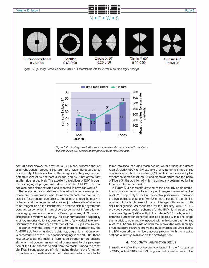
In Figure 5, a schematic drawing of the chief ray angle emula-tion is provided along with actual pupil images measured on the AIMS™ EUV prototype tool for the central position (x=0 mm) and the two outmost positions (x=±52 mm): to notice is the shifting position of the bright area of the pupil image with respect to its dark background. As requested by the industry, AIMS™ EUV provides several design schemes for the EUV illumination of the mask (see Figure 6): differently to the older AIMS™ tools, in which different illumination schemes can be selected within one single sigma stick to be manually inserted within the beam path, on the AIMS™ EUV one illumination scheme is provided with each ap-erture support. Figure 6 shows the pupil images acquired during the EMI consortium members access program with the imaging settings currently available on the prototype tool.
4. Productivity Qualification Status
Immediately after the successful tool launch in the first quarter of 2015, in April 2015 the EMI program participant access to the
Figure 7. Productivity qualification status: run rate and total number of focus stacks acquired during EMI participant companies access measurements.
Figure 6. Pupil images acquired on the AIMS™ EUV prototype with the currently available sigma settings.
Volume 32, Issue 1 Page 5
N • E • W • S

AIMS™ EUV started, in which participating companies deliver EUV masks to ZEISS to be loaded and measured onto the tool. To date, 5 measurement campaigns have been successfully carried out, in which more than a thousand focus stacks were already delivered by the ZEISS AIMS EUV team to the EMI participant companies. The program has the double advantage and importance to provide early access (tool has not yet fully reached the final specifications) to an EUV actinic review tool to the EMI participants, as well as providing application learning experience for the ZEISS team along the development path towards the achievement of final specifica-tions of AIMS™ EUV platform.
Figure 7 shows the actual results in terms of total number of stacks acquired (histogram) and productivity run rate (green line) achieved by the AIMS™ EUV prototype tool during the first five customer measurement blocks (block 4 and 5 combined): these results are based on a mix of low and high pupil fill measurements, therefore a direct comparison with the specification Table provided in Figure 3 cannot be made.
The statistics reported in Figure 7 shows a continuous improve-ment on stack acquisition run-rate, which was achieved through software development process and tool sequences optimization. The current status does not fulfill the final productivity requirement yet, but it already provides sufficient throughput performance for
optimizations of CD reproducibility during the ongoing calibration and tuning phase.
5. Performance Qualification Status
Some calibration measurements as well as information derived from the customer access data allow to draw preliminary conclu-sions on the status of the performance qualification with respect to key deliverables, e.g. CD reproducibility and EUV optics performance.
Figure 8 shows the CD reproducibility results from a champion dataset measured during one of the measurement blocks opened to the EMI members. An horizontal lines and spaces array as il-lustrated in the left panel of Figure 8 was measured for ten times on a customer test mask, from which 25 Regions of Interest (ROIs) were subsequently analyzed for CD measurements. The right panel of the same Figure shows the CD Reproducibility values (in terms of 3 times the standard deviation of the 10 measurements) for the ROIs 1 to 25, in which the highest value was found to be lower than the specification boundary of 1.5 nm. This champion dataset, as well as other champion datasets of 20 repeats, clearly indicate the potential to reach in-spec performance. Within the running calibration and tuning phase the continuous stabilization
Figure 8. CD Reproducibility champion results from EMI access measurements.
Figure 9. Metrology capability results of the AIMS™ EUV prototype system.
Page 6 Volume 32, Issue 1
N • E • W • S

of current champion performance will be of focus.Besides run rate and CD reproducibility, the quality of the EUV
optics has also been measured. The first tool internal aberrations metrology has been tested, with the metrology reproducibility measured to be about 10 times smaller than the tool aberration specification level (RMS for the wavefront error measured through the extraction of the Zernikes values Z5-Z37, see Figure 9).
Therefore, it can be safely stated that the metrology capability for optics tuning has been successfully achieved. Also the first results on the tool aberration level (not shown in Figure 9) indicate safe initial in-spec tool aberration performance.
6. Status and Summary
In this work, the progress of the AIMS™ EUV project has been reported, and the status of the prototype tool as well as the first three customer tools shown. Tool adjustments and calibrations, as well as first tool qualifications are at this date being carried out on the AIMS™ EUV prototype tool, for which the fundamental mask imaging and handling capabilities have been successfully achieved. This current phase will lead towards the automation milestone (see Figure 1), from which further fine tuning and stabi-lization will bring the tool to meet final specification.
From April 2015 the EMI program participants access phase is successfully running on the AIMS™ EUV prototype parallel to other development activities. From internal qualification and customer measurements some first key tests could be performed: the first productivity results on the run-rate indicate sufficient current performance to continue in optimization for CD reproducibility. In addition, the first CD reproducibility champion data show potential for reaching specification performance. Besides, the initial optics
qualification has been carried out and the tool internal aberration metrology capability verified.
7. Acknowledgements
The authors would like to thank SEMATECH and the EMI con-sortium for their support and contributions to the AIMSTM EUV project.
8. References1. A. Erdmann, P. Evanschitzky, T. Bret, and R. Jonckheere, Proc. SPIE
8322, Extreme Ultraviolet (EUV) Lithography III, 83220E (March 29, 2012); doi:10.1117/12.916411.
2. I. Mochi, K.A. Goldberg, R. Xie, P.Y. Yan, and K. Yamazoe, Proc. SPIE 7969, Extreme Ultraviolet (EUV) Lithography II, 79691X (April 07, 2011); doi:10.1117/12.881652.
3. D. Hellweg, J. Ruoff, A. Herkommer, J. Stuhler, T. Ihl, H. Feldmann, M. Ringel, U. Stroßner, S. Perlitz, and W. Harnisch, Proc. of SPIE - The International Society for Optical Engineering (Impact Factor: 0.2). 03/2011; DOI: 10.1117/12.879422.
4. A. Garetto, R. Capelli, K. Magnusson, J.H. Peters, S. Perlitz, U. Matejka, D. Hellweg, M. Weiss, and M. Goldstein, Proc. SPIE 9235, Photomask Technology 2014, 92350N (October 29, 2014); doi:10.1117/12.2068308.
5. R. Capelli, A. Garetto, K. Magnusson, and T. Scherubl, SPIE 9231, 30th European Mask and Lithography Conference, 923109 (17 October 2014); doi: 10.1117/12.2067578.
6. M. Weiss, D. Hellweg, J.H. Peters, S. Perlitz, A. Garetto, and M. Goldstein, SPIE 9048, Extreme Ultraviolet (EUV) Lithography V, 90480X (24 April 2014); doi: 10.1117/12.2046302.
Volume 32, Issue 1 Page 7
N • E • W • S

N • E • W • S
Sponsorship OpportunitiesSign up now for the best sponsorship
opportunities
Advanced Lithography 2016 — Contact: Lara Miles, Tel: +1 360 685 5537;
Photomask 2016 — Contact: Lara Miles, Tel: +1 360 685 5537;
Advertise in the BACUS News!
The BACUS Newsletter is the premier publication serving the photomask industry. For information on how to advertise, contact:
Lara MilesTel: +1 360 685 5537
BACUS Corporate Members
Acuphase Inc.American Coating Technologies LLCAMETEK Precitech, Inc.Berliner Glas KGaA Herbert Kubatz
GmbH & Co.FUJIFILM Electronic Materials U.S.A., Inc.Gudeng Precision Industrial Co., Ltd.Halocarbon ProductsHamaTech APE GmbH & Co. KGHitachi High Technologies America, Inc.JEOL USA Inc.Mentor Graphics Corp.Molecular Imprints, Inc.Panavision Federal Systems, LLCProfilocolore SrlRaytheon ELCAN Optical TechnologiesXYALIS
■ ARM Sizes Up Moore’s Law On EUV and Near-Threshold Computing
Rick Merritt, EETimesEUV lithography still raises skepticism, as it may not be ready for the 7nm node. Beyond 7nm, EUV may require the dreaded multiple patterning, and thus lithography-enabled cost scaling at 5nm and below is uncertain. Another challenge is that engineers can create chips with more transistors than they can afford to power. The so-called dark-silicon problem requires breakthroughs dealing with parasitics and scaling on-chip wires. Below 14nm, half of the power and performance can be lost in the wires, while they were minor issues just a few nodes ago. Reliability is another growing problem. Nagging effects such as bias temperature instability, random telegraph noise and soft error rates may dictate a costly design for resilience. When engineers craft blocks using deep neural networks, the blends of processing and memory may require changes in separate approaches. Research in near-threshold computing (NTC) holds hope, especially for a rising tide of ultra-low power devices for the Internet of Things. RF analog chips could lead optimizing NTC, which could then be applied to give digital processors “acceptable” performance. The workload is high because today’s design flow can benefit more from optimization of NTC voltage regulators that could change the calculus of low energy design. At the same time, printed electronics are reaching feature sizes and integration capabilities on par with microprocessors of the 1970s. On the other hand, the size of the existing semiconductor industry makes it difficult for a potential disruption to arise independently from the existing ecosystem.
■ Samsung Wants to be in Your Next Car
Charles Poladian, International Business TimesSamsung has entered the automotive industry focusing on self-driving cars, to develop entertainment, autonomous driving and satellite navigation components. The restructuring follows news of slumping mobile sales for a second straight year. Analysts praised the move, citing Samsung could be an industry leader. With cars getting smarter each year, the need for chips and advanced electronics is becoming a priority. Samsung is participating in the Audi Progressive SemiConductor Program (PSCP) as a memory supplier. Industry analysts Gartner Inc. indicates that the global automotive semiconductor market will grow to $32.7 billion in revenue in 2016 and the automotive memory market will hit $1.5 billion in 2016. Samsung faces stiff competition from Apple and LG Electronics Inc. The South Korean company has already partnered with General Motors. LG provided the electric drive motor, battery cells, infotainment center and eight other components. Google-backed Android Auto is also a player in the in-vehicle infotainment market, as is Microsoft’s Windows in the Car.
■ Taming Mask Metrology
Mark Lapedus, Semiconductor EngineeringMask metrology is becoming a challenge. The metrology numbers per mask are exploding, some customers want to measure 5,000 places, said Naoya Hayashi, a fellow at Dai Nippon Printing (DNP): the CD and registration overlay inside the die. Turnaround time (TAT) is three times for a 22nm mask compared to a 250nm reticle. Mask makers can make do with their current metrology tools, but want faster tools with in-die capabilities, and in the future, multi-beam tools, CD-SEMs with simulation capabilities and EUV metrology. As masks become more complex, one is spending a lot of time with metrology and inspection, said Thomas Faure, a technical staff member at GlobalFoundries, at the recent SPIE Photomask conference. The total time for inspection could run 18 hours, double the time as compared to several years ago, as leading-edge mask is inspected for defects at least three times during the flow. Then, focus shifts to the hot spot errors and a large amount of data is required to sort out the problems. The CD-SEM is sufficient to measure traditional mask shapes but it is struggling to keep up amid the shift towards more complex patterns and shapes. Most complex mask patterns don’t have uniform CDs after OPC or inverse lithography. It requires 3D litho simulation with SEM imaging, which, in turn, provides two new capabilities for the CD-SEM—mask plane metrology and wafer plane metrology. Toolmakers are developing multi-beam systems for wafer and EUV mask inspection. But a viable multi-beam system is not expected to appear for several years. “Generally, in the mask, we cannot inspect everywhere,” said Banqiu Wu, principal member of the technical staff and chief technology officer for the Mask and TSV Etch Division at Applied Materials. “You only measure some points. We assume if we control this area when we design the mask, we can control the whole thing. But because of pattern density, and proximity effects, maybe we need more measurement points.” The good news is that the industry is working on a new class of EUV metrology tools. But even with current and future metrology tools, EUV mask TATs, along with costs, will likely soar.
Page 8 Volume 32, Issue 1
N • E • W • S
Industry Briefs

2016
SPIE Advanced Lithography21-25 February 2016 San Jose Convention Center San Jose, California, USAwww.spie.org/al
Late abstracts will be considered by the chairs. Contact Pat Wight at [email protected]
SPIE Photomask Technology12-14 September 2016San Jose Marriott and San Jose Convention CenterSan Jose, California, USA www.spie.org/pm
Abstract Due Date: 28 March 2016
Corporate Membership Benefits include:■ 3-10 Voting Members in the SPIE General Membership,
depending on tier level
■ Subscription to BACUS News (monthly)
■ One online SPIE Journal Subscription
■ Listed as a Corporate Member in the BACUS Monthly Newsletter www.spie.org/bacushome
C a l e n d a r
About the BACUS GroupFounded in 1980 by a group of chrome blank users wanting a single voice to interact with suppliers, BACUS has grown to become the largest and most widely known forum for the exchange of technical information of interest to photomask and reticle makers. BACUS joined SPIE in January of 1991 to expand the exchange of information with mask makers around the world.
The group sponsors an informative monthly meeting and newsletter, BACUS News. The BACUS annual Photomask Technology Symposium covers photomask technology, photomask processes, lithography, materials and resists, phase shift masks, inspection and repair, metrology, and quality and manufacturing management.
Individual Membership Benefits include:■ Subscription to BACUS News (monthly)
■ Eligibility to hold office on BACUS Steering Committee
www.spie.org/bacushome
You are invited to submit events of interest for this calendar. Please send to [email protected]; alternatively,
email or fax to SPIE.
h
h
Join the premier professional organization for mask makers and mask users!
SPIE is the international society for optics and photonics, an educational not-for-profit organization founded in 1955 to advance light-based science and technology. The Society serves nearly 264,000 constituents from approximately 166 countries, offering conferences and their published proceedings, continuing education, books, journals, and the SPIE Digital Library in support of interdisciplinary information exchange, professional networking, and patent precedent. SPIE provided more than $5.2 million in support of education and outreach programs in 2015. www.spie.org
International HeadquartersP.O. Box 10, Bellingham, WA 98227-0010 USA Tel: +1 360 676 3290 Fax: +1 360 647 [email protected] • www.SPIE.org
Shipping Address1000 20th St., Bellingham, WA 98225-6705 USA
Managed by SPIE Europe 2 Alexandra Gate, Ffordd Pengam, Cardiff, CF24 2SA, UK Tel: +44 29 2089 4747 Fax: +44 29 2089 [email protected] • www.spieeurope.org
Volume 32, Issue 1 Page 9
N • E • W • S