Embed Size (px)
Citation preview
Ann. Phys. (Leipzig) 10 (2001) 1–2, 61 – 74
Photoemission spectroscopy in solids
T.-C. Chiang1, F. Seitz2
1Department of Physics, University of Illinois, 1110 West Green StreetUrbana, IL 61801-3080, USA2Materials Research Laboratory, University of Illinois, 104 South Goodwin AvenueUrbana, IL 61801-2902, [email protected]
Received 2 Aug. 2000, accepted 29 Sep. 2000 by C. Thomsen
Abstract. The photoelectric effect was discovered and explained in terms of quantumphysics about a hundred years ago. Today, photoemission spectroscopy using vacuum ultra-violet radiation and x-rays is an important tool for studying the electronic properties andatomic structure of solids. This paper reviews the development of an understanding of thephotoemission process and the basic applications of photoemission spectroscopy in solids,including band structure determination, studies of quasiparticle properties, and core levelspectroscopy.
Keywords: photoemission, photoelectron, spectroscopy, band structure, solids
PACS: 79.60, 71.20
1 Introduction
The photoelectric effect was discovered in 1887 by H. Hertz in a study of electric sparksacross gaps [1]. He observed that sparks could be triggered by ultraviolet illuminationgenerated by a nearby spark. This illumination was shown to lead to electron emissionthat aided spark formation. A quantitative explanation for the ensuing observationsof light-induced electron emission was given by Albert Einstein in 1905 [2], whosetheory of the photoelectric effect was a cornerstone for modern quantum mechanics.He was awarded the Nobel Prize in 1921 for this work. Two important concepts wereintroduced by his theory. First, light is made of quanta (photons), and the energyof each photon is given by the product of Planck’s constant and the frequency of thelight hν . Second, an electron can absorb a photon and emit with the full final energy.It was later recognized that such electron emission carried useful information about
the electronic structure of solids [3–8]. Since the mean free path of photoelectronsranges typically from a few Angstroms to a few tens of Angstroms, photoemissionmeasurements are surface sensitive. Early experiments were troubled by contami-nation and the uncertain states of the sample surface. It took about 50 years afterEinstein’s theory before the widespread deployment of ultrahigh vacuum techniques inresearch that allowed experiments on samples sufficiently clean to yield reproducibleand meaningful results. Both surface and volume effects were reported in experimental
62 Ann. Phys. (Leipzig) 10 (2001) 1–2
and theoretical studies, and there was much confusion about the relative importanceof these effects in the early years.In the 1960’s synchrotron radiation sources became available [4, 9], which spurred
a rapid development and growth of photoemission as a major research field. Thecontinuous tunability over a wide energy range and high intensity from such sourcesfacilitated experiments on a variety of systems, including solids, surfaces, and ad-sorbates. Another important development was highly efficient electrostatic electronenergy analyzers that allowed detection of the typically fairly weak photoemission sig-nal within a reasonable time. Concomitant to the rapid expansion in experimentaleffort, theories were developed to explain the photoemission results in terms of basicelectronic properties and atomic structure of solids and surfaces.Today, third-generation synchrotron radiation sources equipped with magnetic in-
sertion devices (undulators and wigglers) offer unprecedented brightness, and plans arealready underway for fourth-generation machines and free-electron lasers. For somematerials, the beam intensity available now is already high enough to cause damage.As for the detectors, two-dimensional or multi-channel detection has become com-monplace. Compared with early experiments with an energy resolution of ∼ 1 eVand an angular resolution of a few degrees, modern instruments are orders of magni-tude better, with energy resolution of ∼ 1 meV and angular resolution approaching0.01◦. These capabilities allow highly precise measurements of subtle effects that gobeyond the usual single-particle picture, providing critical tests of the foundation ofmany-body quantum theory including the interactions of electrons (or quasiparticles)among themselves and with other elementary and collective excitations. These capa-bilities also set stringent limits on levels of impurity and imperfection in materials thatcan be tolerated. Impurities and defects near a surface tend to smear out spectral fea-tures, and efforts to improve resolution further would be useless unless the materials ofinterest can be prepared with correspondingly improved quality. Materials preparationand control at the atomic level is indeed an important emphasis in modern materialsresearch.This article reviews the development and status of some important basic topics of
photoemission spectroscopy in solids, including band structure determination, studiesof quasiparticle properties, and core level spectroscopy. Limited by space, this reviewhas to be selective, and the selection is to emphasize basic concepts in solid statephysics based on the quantum theory.
2 Photoemission from Valence Electrons
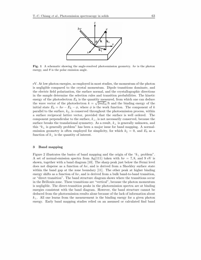
Valence electrons are found within ∼ 10 eV of the Fermi level. They are responsible forthe chemical bonding of atoms in a solid. A basic description of these electronic statesis the band structure, which is of central importance to solid state physics. Despite themany advances made in theoretical band structure calculations over the years, therewere no experimental methods for band mapping, or direct determination of the bandstructure, until the advent of angle-resolved photoemission and development of a goodunderstanding of the photoemission process. Figure 1 shows the typical experimentalgeometry. The energy of the photon hν can range from a few eV to over a thousand
T.-C. Chiang et al., Photoemission spectroscopy in solids 63
x
y
z
hν
k
e
k⊥
kR
θ
Fig. 1 A schematic showing the angle-resolved photoemission geometry. hν is the photonenergy, and θ is the polar emission angle.
eV. At low photon energies, as employed in most studies, the momentum of the photonis negligible compared to the crystal momentum. Dipole transitions dominate, andthe electric field polarization, the surface normal, and the crystallographic directionsin the sample determine the selection rules and transition probabilities. The kineticenergy of the photoelectron Ek is the quantity measured, from which one can deducethe wave vector of the photoelectron k =
√2mEk/h and the binding energy of the
initial state Eb = hν − Ek − φ, where φ is the work function. The component of kparallel to the surface, k‖, is conserved throughout the photoemission process, withina surface reciprocal lattice vector, provided that the surface is well ordered. Thecomponent perpendicular to the surface, k⊥, is not necessarily conserved, because thesurface breaks the translational symmetry. As a result, k⊥ is generally unknown, andthis “k⊥ is generally problem” has been a major issue for band mapping. A normal-emission geometry is often employed for simplicity, for which k‖ = 0, and Eb as afunction of k⊥ is the quantity of interest.
3 Band mapping
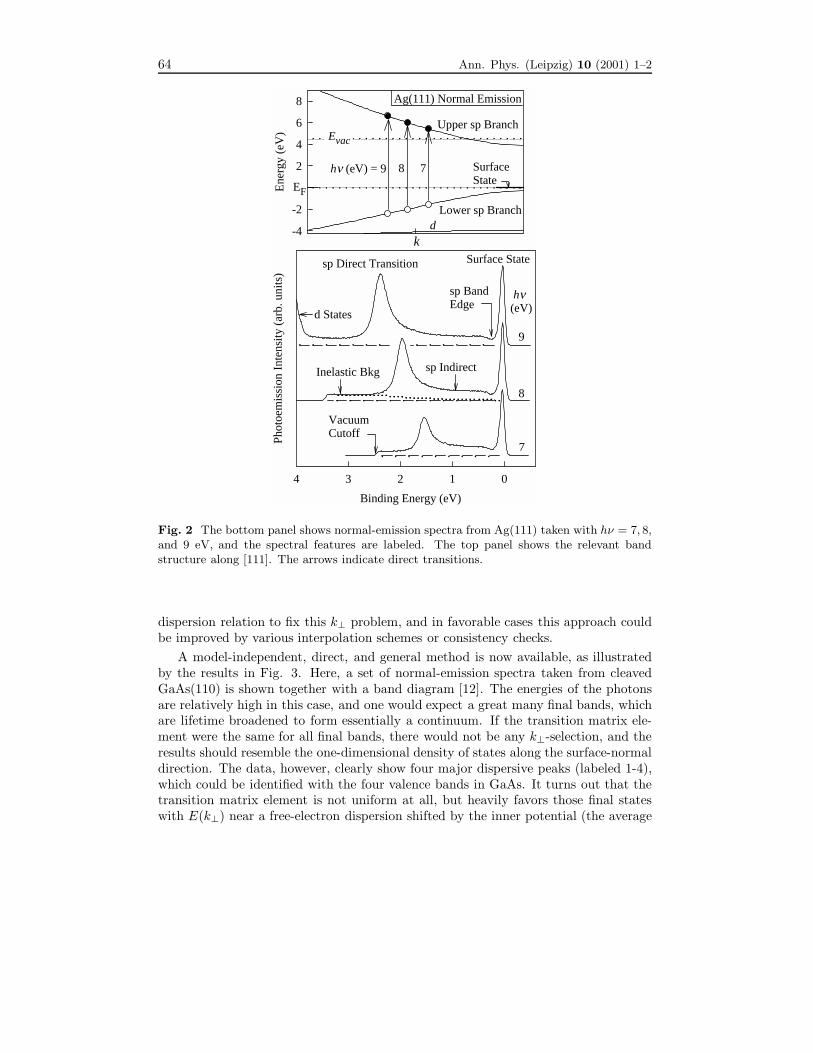
Figure 2 illustrates the basics of band mapping and the origin of the “k⊥ problem”.A set of normal-emission spectra from Ag(111) taken with hν = 7, 8, and 9 eV isshown, together with a band diagram [10]. The sharp peak just below the Fermi leveldoes not disperse as a function of hν , and is derived from a Shockley surface statewithin the band gap at the zone boundary [11]. The other peak at higher bindingenergy shifts as a function of hν , and is derived from a bulk band-to-band transition,or “direct transition”. The band structure diagram shows where the transitions occurin the Brillouin zone. These transitions are “vertical”, because the photon momentumis negligible. The direct-transition peaks in the photoemission spectra are at bindingenergies consistent with the band diagram. However, the band structure cannot bededuced from the photoemission results alone because of the lack of information aboutk⊥. All one learns from the measurement is the binding energy for a given photonenergy. Early band mapping studies relied on an assumed or calculated find band
64 Ann. Phys. (Leipzig) 10 (2001) 1–2
k
Ene
rgy
(eV
)
-4
-2
2
4
6
8
EF
Ag(111) Normal Emission
Upper sp Branch
Lower sp Branchd
SurfaceState
hν (eV) = 9 8 7
Binding Energy (eV)
01234
Phot
oem
issi
on I
nten
sity
(ar
b. u
nits
)
Surface Statesp Direct Transition
d States
sp Band Edge
hν(eV)
7
8
9
VacuumCutoff
sp Indirect
Evac
Inelastic Bkg
Fig. 2 The bottom panel shows normal-emission spectra from Ag(111) taken with hν = 7, 8,and 9 eV, and the spectral features are labeled. The top panel shows the relevant bandstructure along [111]. The arrows indicate direct transitions.
dispersion relation to fix this k⊥ problem, and in favorable cases this approach couldbe improved by various interpolation schemes or consistency checks.A model-independent, direct, and general method is now available, as illustrated
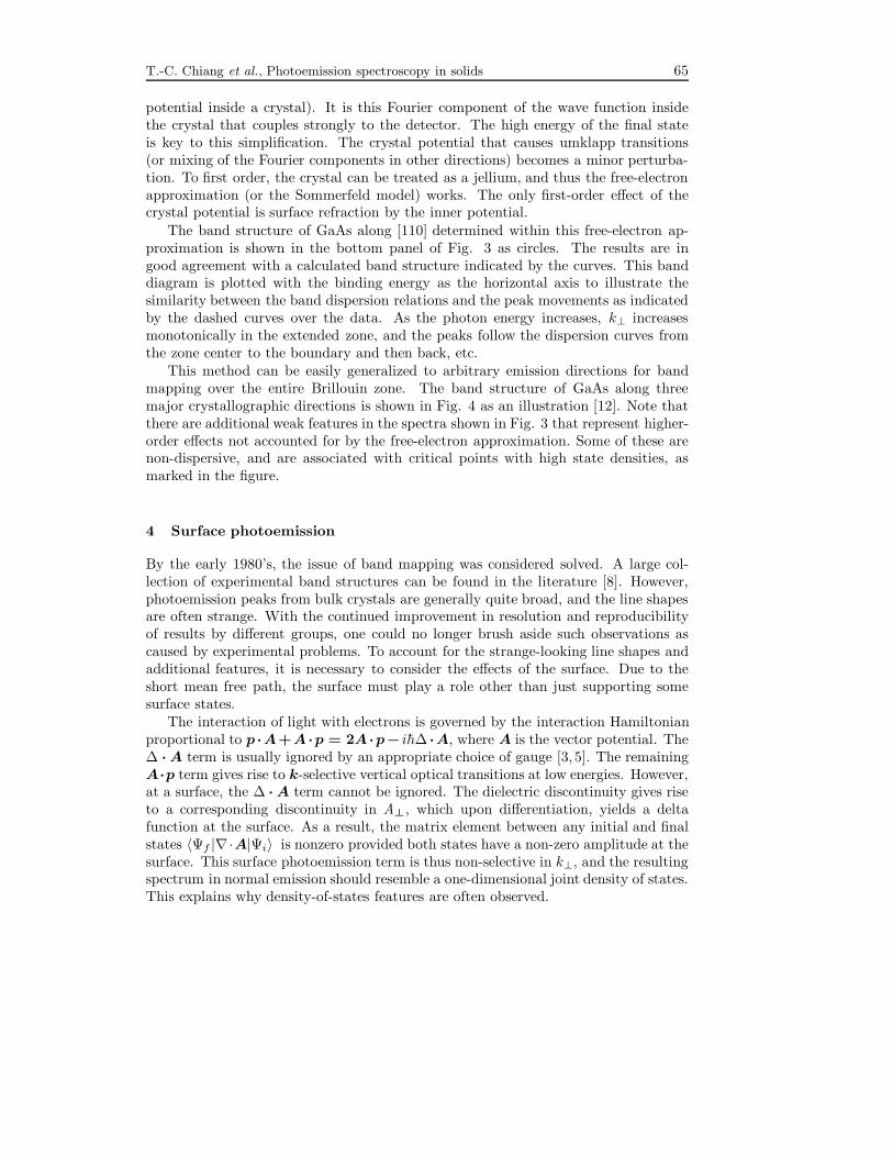
by the results in Fig. 3. Here, a set of normal-emission spectra taken from cleavedGaAs(110) is shown together with a band diagram [12]. The energies of the photonsare relatively high in this case, and one would expect a great many final bands, whichare lifetime broadened to form essentially a continuum. If the transition matrix ele-ment were the same for all final bands, there would not be any k⊥-selection, and theresults should resemble the one-dimensional density of states along the surface-normaldirection. The data, however, clearly show four major dispersive peaks (labeled 1-4),which could be identified with the four valence bands in GaAs. It turns out that thetransition matrix element is not uniform at all, but heavily favors those final stateswith E(k⊥) near a free-electron dispersion shifted by the inner potential (the average
T.-C. Chiang et al., Photoemission spectroscopy in solids 65
potential inside a crystal). It is this Fourier component of the wave function insidethe crystal that couples strongly to the detector. The high energy of the final stateis key to this simplification. The crystal potential that causes umklapp transitions(or mixing of the Fourier components in other directions) becomes a minor perturba-tion. To first order, the crystal can be treated as a jellium, and thus the free-electronapproximation (or the Sommerfeld model) works. The only first-order effect of thecrystal potential is surface refraction by the inner potential.The band structure of GaAs along [110] determined within this free-electron ap-
proximation is shown in the bottom panel of Fig. 3 as circles. The results are ingood agreement with a calculated band structure indicated by the curves. This banddiagram is plotted with the binding energy as the horizontal axis to illustrate thesimilarity between the band dispersion relations and the peak movements as indicatedby the dashed curves over the data. As the photon energy increases, k⊥ increasesmonotonically in the extended zone, and the peaks follow the dispersion curves fromthe zone center to the boundary and then back, etc.This method can be easily generalized to arbitrary emission directions for band
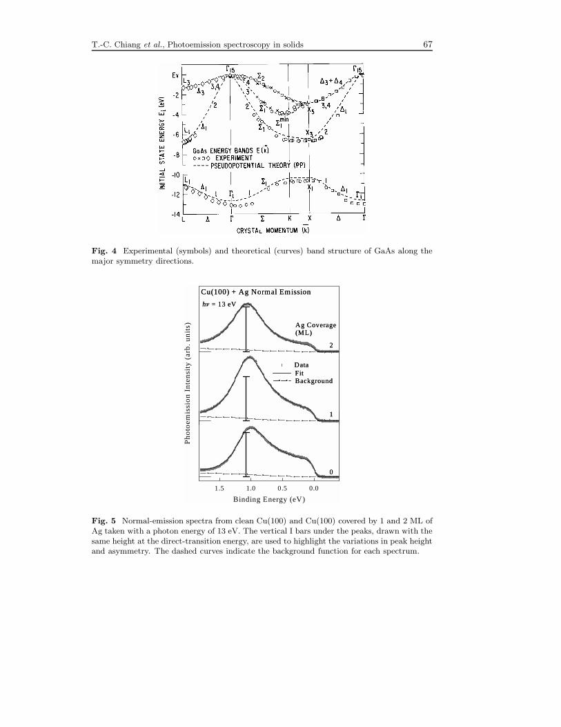
mapping over the entire Brillouin zone. The band structure of GaAs along threemajor crystallographic directions is shown in Fig. 4 as an illustration [12]. Note thatthere are additional weak features in the spectra shown in Fig. 3 that represent higher-order effects not accounted for by the free-electron approximation. Some of these arenon-dispersive, and are associated with critical points with high state densities, asmarked in the figure.
4 Surface photoemission
By the early 1980’s, the issue of band mapping was considered solved. A large col-lection of experimental band structures can be found in the literature [8]. However,photoemission peaks from bulk crystals are generally quite broad, and the line shapesare often strange. With the continued improvement in resolution and reproducibilityof results by different groups, one could no longer brush aside such observations ascaused by experimental problems. To account for the strange-looking line shapes andadditional features, it is necessary to consider the effects of the surface. Due to theshort mean free path, the surface must play a role other than just supporting somesurface states.The interaction of light with electrons is governed by the interaction Hamiltonian
proportional to p ·A+A ·p = 2A ·p− ih∆ ·A, where A is the vector potential. The∆ · A term is usually ignored by an appropriate choice of gauge [3, 5]. The remainingA·p term gives rise to k-selective vertical optical transitions at low energies. However,at a surface, the ∆ · A term cannot be ignored. The dielectric discontinuity gives riseto a corresponding discontinuity in A⊥, which upon differentiation, yields a deltafunction at the surface. As a result, the matrix element between any initial and finalstates 〈Ψf |∇·A|Ψi〉 is nonzero provided both states have a non-zero amplitude at thesurface. This surface photoemission term is thus non-selective in k⊥, and the resultingspectrum in normal emission should resemble a one-dimensional joint density of states.This explains why density-of-states features are often observed.
66 Ann. Phys. (Leipzig) 10 (2001) 1–2
BINDING ENERGY (eV)051015
k /k ΓK
X
0
1
Fig. 3 The top panel shows normal-emission spectra taken from cleaved GaAs(110) forvarious photon energies as indicated. The dashed curves indicate the dispersions of thevalence peaks. The features A and A’ are Auger transitions derived from the Ga and As corelevels, respectively. The vertical dotted lines indicate density-of-state features as labeled.The bottom panel shows the experimental (circles) and theoretical (curves) band structurealong [110].
T.-C. Chiang et al., Photoemission spectroscopy in solids 67
Fig. 4 Experimental (symbols) and theoretical (curves) band structure of GaAs along themajor symmetry directions.
Binding Energy (eV)
0.00.51.01.5
Ph
oto
emis
sio
n I
nte
nsi
ty (
arb
. u
nit
s) Ag Coverage(ML)
2
1
0
h� = 13 eV
Cu(100) + Ag Normal Emission
Fit| Data
Background
Ag Coverage(ML)
2
1
0
h� = 13 eV
Cu(100) + Ag Normal Emission
Fit| Data
Background
Fig. 5 Normal-emission spectra from clean Cu(100) and Cu(100) covered by 1 and 2 ML ofAg taken with a photon energy of 13 eV. The vertical I bars under the peaks, drawn with thesame height at the direct-transition energy, are used to highlight the variations in peak heightand asymmetry. The dashed curves indicate the background function for each spectrum.
68 Ann. Phys. (Leipzig) 10 (2001) 1–2
k/kΓX
0.5 0.6 0.7 0.8 0.9 1.0E
nerg
y (e
V)
0
5
10
15
hν = 14 eV
Ag(100) Normal Emission
Γi (highly exaggerated)
γΓf
Fig. 6 Band diagram for Ag(100). The vertical arrow indicates a direct transition at aphoton energy of 14 eV. The horizontal dashed line is at the Fermi level. The lifetimebroadening of each band is indicated schematically by the dashed curves parallel to the band.
The photoemission spectrum is, however, not a simple sum of the bulk and surfaceintensities. The total matrix element, proportional to 〈Ψf |2A ·p− ih∇·A|〉, involvesa phased sum of the two contributions. Upon squaring to yield the intensity, there canbe an interference effect between the bulk contribution, which is a peak by itself, andthe surface contribution, which is generally a continuum spanning the entire valenceband [10]. The result is then a Fano-like profile. The spectra in Fig. 2 offer anexample; each direct-transition peak is obviously asymmetric. The bulk and surfacecontributions interfere constructively on the low binding energy side, giving rise to abroad emission plateau, traditionally known as the indirect-transition plateau, whichextends towards lower binding energies all the way to the band edge near the surfacestate. On the high binding energy side of the direct-transition peak, the intensity ismuch lower due to destructive interference.
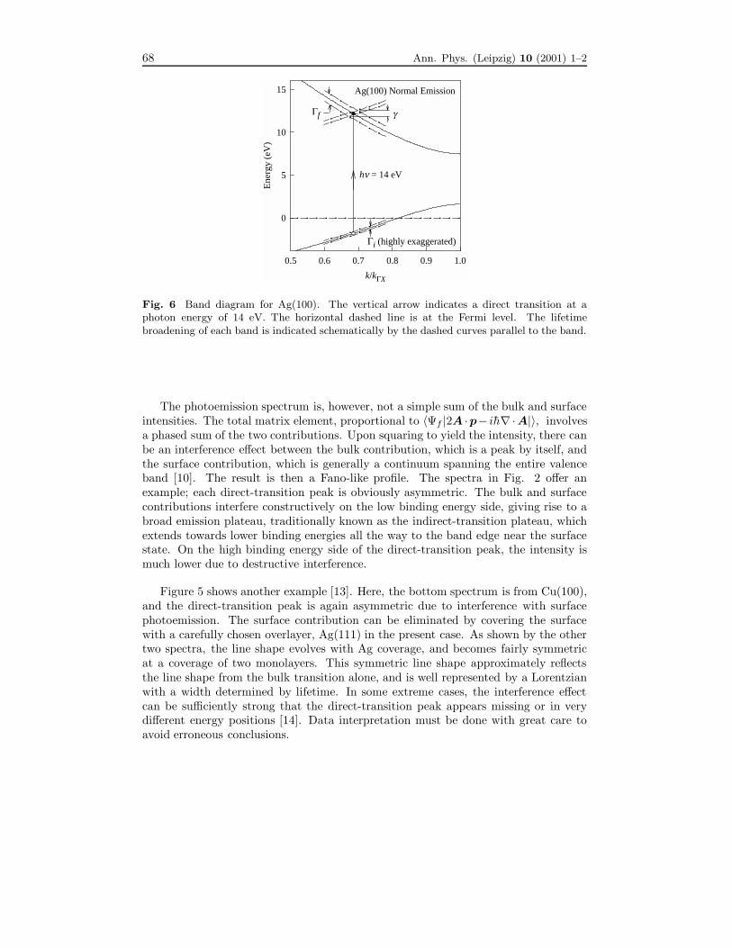
Figure 5 shows another example [13]. Here, the bottom spectrum is from Cu(100),and the direct-transition peak is again asymmetric due to interference with surfacephotoemission. The surface contribution can be eliminated by covering the surfacewith a carefully chosen overlayer, Ag(111) in the present case. As shown by the othertwo spectra, the line shape evolves with Ag coverage, and becomes fairly symmetricat a coverage of two monolayers. This symmetric line shape approximately reflectsthe line shape from the bulk transition alone, and is well represented by a Lorentzianwith a width determined by lifetime. In some extreme cases, the interference effectcan be sufficiently strong that the direct-transition peak appears missing or in verydifferent energy positions [14]. Data interpretation must be done with great care toavoid erroneous conclusions.
T.-C. Chiang et al., Photoemission spectroscopy in solids 69
Photoemission from Ag(100)
Binding Energy (eV)
012
������������������� ���������
hν = 13 eVθ = 0°
hν = 11.25 eVθ = 80°
Fig. 7 Angle-resolved photoemission spectra taken with a normal-emission geometry (topcurve) and a grazing-emission geometry (bottom curve). The photon energies, indicated inthe figure, are chosen to yield a direct-transition peak at about the same binding energy.
5 Line widths and quasiparticle lifetimes
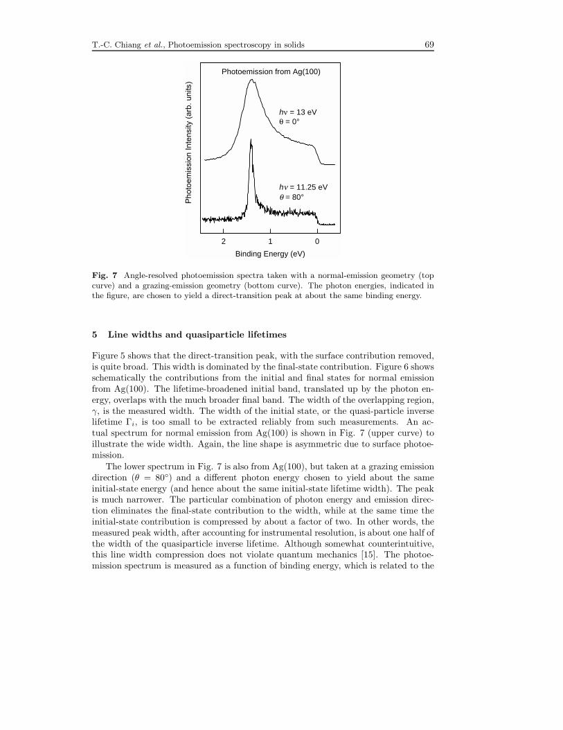
Figure 5 shows that the direct-transition peak, with the surface contribution removed,is quite broad. This width is dominated by the final-state contribution. Figure 6 showsschematically the contributions from the initial and final states for normal emissionfrom Ag(100). The lifetime-broadened initial band, translated up by the photon en-ergy, overlaps with the much broader final band. The width of the overlapping region,γ, is the measured width. The width of the initial state, or the quasi-particle inverselifetime Γi, is too small to be extracted reliably from such measurements. An ac-tual spectrum for normal emission from Ag(100) is shown in Fig. 7 (upper curve) toillustrate the wide width. Again, the line shape is asymmetric due to surface photoe-mission.The lower spectrum in Fig. 7 is also from Ag(100), but taken at a grazing emission
direction (θ = 80◦) and a different photon energy chosen to yield about the sameinitial-state energy (and hence about the same initial-state lifetime width). The peakis much narrower. The particular combination of photon energy and emission direc-tion eliminates the final-state contribution to the width, while at the same time theinitial-state contribution is compressed by about a factor of two. In other words, themeasured peak width, after accounting for instrumental resolution, is about one half ofthe width of the quasiparticle inverse lifetime. Although somewhat counterintuitive,this line width compression does not violate quantum mechanics [15]. The photoe-mission spectrum is measured as a function of binding energy, which is related to the
70 Ann. Phys. (Leipzig) 10 (2001) 1–2
Binding Energy (eV)
01
Pho
toem
issi
on In
tens
ity (
arb.
uni
ts)
71
57
42
27.5
14
Ag/Fe(100)hν = 16 eV
12
42.5
95
Thickness (ML)
28
119
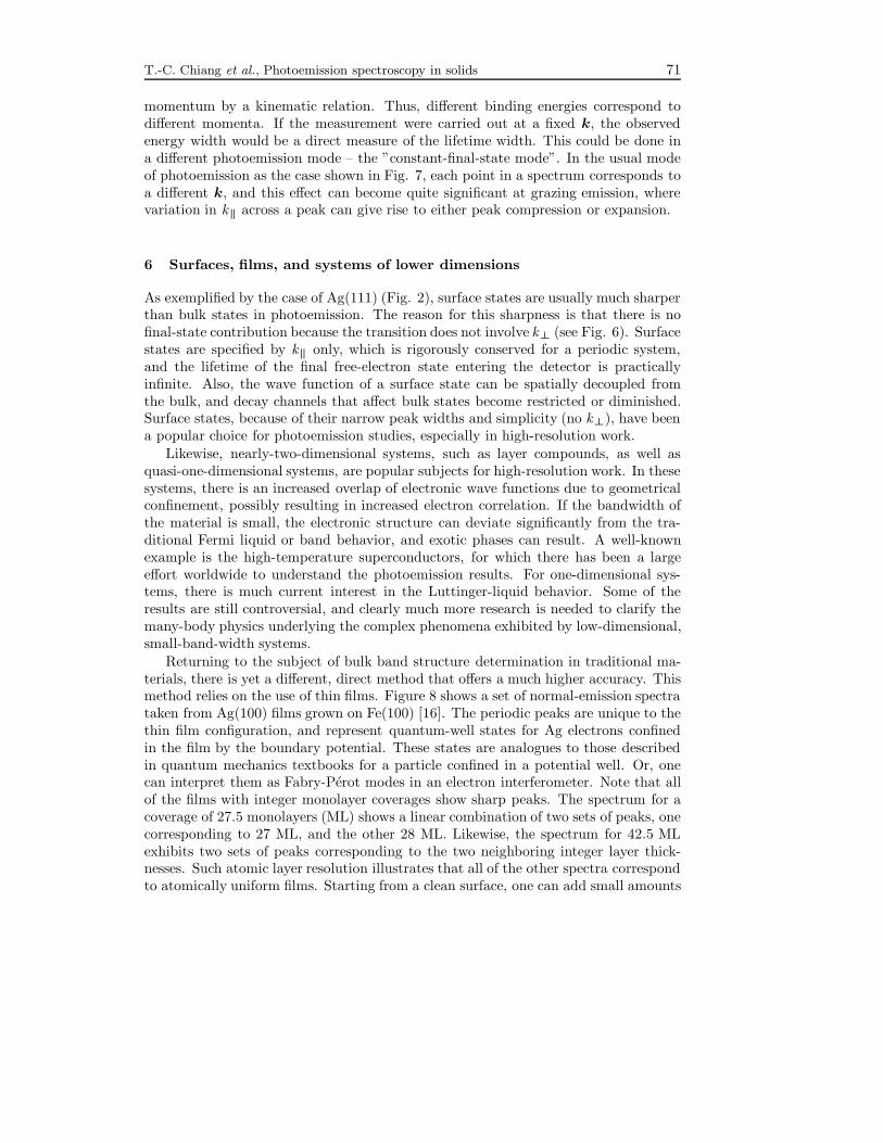
Fig. 8 Normal emission spectra for Ag deposited on Fe(100) at various coverages as indi-cated. The photon energy is hν = 16 eV. The data points are shown as dots, while the fitsto the data and the background functions are shown as curves. The peaks are derived fromquantum well states.
T.-C. Chiang et al., Photoemission spectroscopy in solids 71
momentum by a kinematic relation. Thus, different binding energies correspond todifferent momenta. If the measurement were carried out at a fixed k, the observedenergy width would be a direct measure of the lifetime width. This could be done ina different photoemission mode – the ”constant-final-state mode”. In the usual modeof photoemission as the case shown in Fig. 7, each point in a spectrum corresponds toa different k, and this effect can become quite significant at grazing emission, wherevariation in k‖ across a peak can give rise to either peak compression or expansion.
6 Surfaces, films, and systems of lower dimensions
As exemplified by the case of Ag(111) (Fig. 2), surface states are usually much sharperthan bulk states in photoemission. The reason for this sharpness is that there is nofinal-state contribution because the transition does not involve k⊥ (see Fig. 6). Surfacestates are specified by k‖ only, which is rigorously conserved for a periodic system,and the lifetime of the final free-electron state entering the detector is practicallyinfinite. Also, the wave function of a surface state can be spatially decoupled fromthe bulk, and decay channels that affect bulk states become restricted or diminished.Surface states, because of their narrow peak widths and simplicity (no k⊥), have beena popular choice for photoemission studies, especially in high-resolution work.Likewise, nearly-two-dimensional systems, such as layer compounds, as well as
quasi-one-dimensional systems, are popular subjects for high-resolution work. In thesesystems, there is an increased overlap of electronic wave functions due to geometricalconfinement, possibly resulting in increased electron correlation. If the bandwidth ofthe material is small, the electronic structure can deviate significantly from the tra-ditional Fermi liquid or band behavior, and exotic phases can result. A well-knownexample is the high-temperature superconductors, for which there has been a largeeffort worldwide to understand the photoemission results. For one-dimensional sys-tems, there is much current interest in the Luttinger-liquid behavior. Some of theresults are still controversial, and clearly much more research is needed to clarify themany-body physics underlying the complex phenomena exhibited by low-dimensional,small-band-width systems.Returning to the subject of bulk band structure determination in traditional ma-
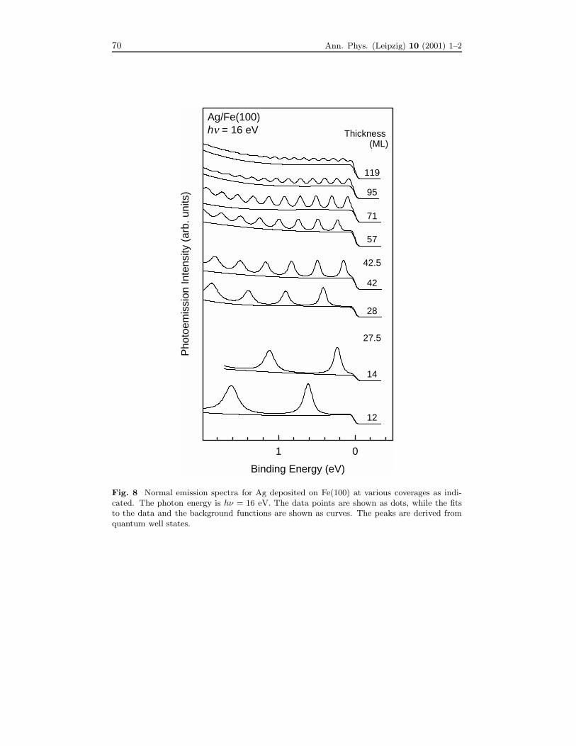
terials, there is yet a different, direct method that offers a much higher accuracy. Thismethod relies on the use of thin films. Figure 8 shows a set of normal-emission spectrataken from Ag(100) films grown on Fe(100) [16]. The periodic peaks are unique to thethin film configuration, and represent quantum-well states for Ag electrons confinedin the film by the boundary potential. These states are analogues to those describedin quantum mechanics textbooks for a particle confined in a potential well. Or, onecan interpret them as Fabry-Perot modes in an electron interferometer. Note that allof the films with integer monolayer coverages show sharp peaks. The spectrum for acoverage of 27.5 monolayers (ML) shows a linear combination of two sets of peaks, onecorresponding to 27 ML, and the other 28 ML. Likewise, the spectrum for 42.5 MLexhibits two sets of peaks corresponding to the two neighboring integer layer thick-nesses. Such atomic layer resolution illustrates that all of the other spectra correspondto atomically uniform films. Starting from a clean surface, one can add small amounts
72 Ann. Phys. (Leipzig) 10 (2001) 1–2
of Ag to build up a film one monolayer at a time, and this layer counting provides anabsolute determination of film thicknesses over a wide range.Using such atomically uniform films, one can deduce the band structure and quasi-
particle lifetime from the measured peak positions and peak widths. The peak posi-tions are determined by the interferometer modes, or standing wave patterns in thefilm. Since the film thicknesses are quantized in terms of the atomic layer thickness,the resulting band structure is very accurate. Results for Ag(100) yield a Fermi wavevector accurate to ∼ 0.1%, which challenges the traditional de Haas-van Alphen mea-surement. The measured lifetime width as a function of temperature, film thickness,and binding energy can be analyzed to yield separate contributions from electron-electron scattering, electron-phonon scattering, and electron-defect scattering [16].
7 Photoemission from core electrons
Limited by surface, only brief remarks will be made here. Core levels are deeply bound,atomic-like states, and show little band dispersions. They require higher energy pho-tons for excitation, and hence the technique is often referred to as x-ray photoelectronspectroscopy (XPS). Kai Siegbahn’s group pioneered the field, for which he was awardthe Nobel Prize in 1981. Emission from each core level gives rise to a peak with aunique energy, which is suitable for chemical analysis. As the instrumental resolutionand sensitivity improved, it was noticed that core level emission from metals gave riseto an asymmetric line shape, which was later understood as arising from the many-body response of a Fermi liquid to a sudden creation of a core hole. Also noticedearly on were satellite features due to shake-up transitions involving the excitationsof other electrons or plasmons. Studies of these phenomena contributed much to thedevelopment of many-body physics [3, 5, 7].An important scientific and industrial application of XPS is analysis of surface
composition, also known as Electron Spectroscopy for Chemical Analysis (ESCA).Many commercial machines are employed in industrial and academic research labora-tories worldwide. With sufficient resolution and in favorable cases, one can distinguishdifferent chemical states of a given element as revealed by shifts of core level peak po-sitions [17]. Such chemical shifts are often analyzed in terms of initial-state effects,including charge transfer, and final-state screening effects. Beginning in the late 1970’sand early 1980’s, the experimental resolution became high enough that intrinsic surfacecore level shifts for films and single-crystal substrates were detected [18, 19]. Differ-ent surface reconstructions of the same material can exhibit different core level shifts,and this information is useful for understanding the relationships between the surfaceatomic structure and electronic properties.It was noticed in early work that core level intensities vary as a function of emission
direction and photon energy. Some of these variations reflect the properties of thecore level wave function. Additional variations are due to final-state effects, includingdiffraction. A core electron emitted from an atom is represented by a wave, and can bescattered by nearby atoms. If the emission is from a surface atom on a crystal, one canvisualize this as a wave emanating from a point source being scattered or diffractedby the underlying three-dimensional crystal structure. Since the mean free path of
T.-C. Chiang et al., Photoemission spectroscopy in solids 73
the photoelectron is rather short, only nearby atoms contribute significantly to thediffraction process. Nevertheless, multiple scattering is important, and early studiesoften employed a fitting procedure starting from an assumed model. The methodologyis in many ways similar to that employed in low energy electron diffraction [20].In the past decade or so, there has been an increased understanding of the diffrac-
tion process as well as an increased efficiency in data acquisition and analysis that hasled to the development of photoelectron holography [21]. In this approach, a large setof intensity data taken over many emission directions and excitation photon energies isused as a hologram for direct mathematical inversion to yield an image of atoms nearthe emitter. This model-independent, direct approach holds great promise for routinestructural analysis. An important, related development is the extended fine-structuremeasurement similar to EXAFS, which allows atomic bond-length determination.
8 Concluding remarks and outlook
Photoemission has a long history, with its evolution intimately tied to the developmentof quantum mechanics. Interaction of light with solids and the resulting emission ofelectrons is a complex phenomenon. Each major improvement in experimental ca-pabilities has led to observations of new phenomena and finer details that require adeeper understanding of the underlying physics. This brief review focuses on the basicsof photoemission and its applications in fundamental scientific studies of solids. Spacelimitations forced the omission of many important subjects, such as spin-resolved,time-resolved, spatially-resolved, and multi-photon photoemission. As photon sourcesand electron analyzers become more powerful and more sophisticated, there will un-doubtedly be many more discoveries and surprises. Current emphasis on electroncorrelation effects should lead to a detailed understanding of the many intriguing as-pects of many-body physics, and such understanding is important for the design andapplication of ”complex functional materials” for future generations of devices. Forfundamental scientific research, we hope that one day we would be able to performtime-, spin-, and angle-resolved photoemission from a single specific atom in a solid,thus yielding a complete specification of the electronic and magnetic properties, atomicstructure, and dynamic behavior.
Acknowledgements
Much of the material presented here is based upon work supported by the U. S. Na-tional Science Foundation, under Grant Nos. DMR-99-75470 and DMR-99-75182,the U. S. Department of Energy, Division of Materials Sciences, under Grant No.DEFG02-91ER45439, and the Donors of the Petroleum Research Fund, administeredby the American Chemical Society. The Synchrotron Radiation Center of the Uni-versity of Wisconsin, where much of the work was performed, is supported by theNational Science Foundation under Grant No. DMR-95-31009.

74 Ann. Phys. (Leipzig) 10 (2001) 1–2
References
[1] H. Hertz, Ann. Physik 31 (1887) 983[2] A. Einstein, Ann. Physik 17 (1905) 132[3] Photoemission in Solids I, edited by M. Cardona and L. Ley, Topics in Applied Physics,
Vol. 26, Springer, Berlin, 1978[4] Photoemission in Solids II, edited by M. Cardona and L. Ley, Topics in Applied Physics,
Vol. 27, Springer, Berlin, 1979[5] Photoemission and the Electronic Properties of Surfaces, edited by B. Feuerbacher, B.
Fitton, and R. F. Willis, Wiley, New York, 1978[6] Angle-resolved Photoemission, edited by S. D. Kevan, Studies in Surface Science and
Catalysis, Vol. 74, Elsevier, Amsterdam, 1992[7] S. Hufner, Photoelectron Spectroscopy - Principles and Applications, Springer Series in
Solid-State Science, Vol. 82, Springer, Berlin, 1995[8] Electronic Structure of Solids: Photoemission Spectra and Related Data, edited by A.
Goldmann and E. E. Koch, Landolt-Bornstein, Numerical Data and Functional Rela-tionships in Science and Technology, New Series, Group III, Vol. 23, Springer, Berlin,1989
[9] G. Margaritondo, Introduction to Synchrotron Radiation, Oxford University Press, NewYork, 1988
[10] T. Miller, W. E. McMahon, and T.-C. Chiang, Phys. Rev. Lett. 77 (1996) 1167; T.Miller, E. D. Hansen, W. E. McMahon, and T.-C. Chiang, Surf. Sci. 376 (1997) 32
[11] P. O. Gartland and B. J. Slagsvold, Phys. Rev. B 12 (1975) 4047[12] T.C. Chiang, J. A. Knapp, D. E. Eastman, and M. Aono, Solid State Commun. 31
(1979) 917; T.C. Chiang, J. A. Knapp, M. Aono, and D. E. Eastman, Phys. Rev. B 21(1980) 3513
[13] E. D. Hansen, T. Miller, and T.-C. Chiang, Phys. Rev. Lett. 78 (1997) 2807[14] D. Claesson, S.-A. Lindgren, L. Wallden, and T.-C. Chiang, Phys. Rev. Lett. 82 (1999)
1740[15] E. D. Hansen, T. Miller, and T.-C. Chiang, Phys. Rev. Lett. 80 (1998) 1766[16] J. J. Paggel, T. Miller, and T.-C. Chiang, Science 283 (1999) 1709; Phys. Rev. Lett. 83
(1999) 1415; Phys. Rev. B 61 (2000) 1804[17] S. Hagstrom, C. Nordling, and K. Siegbahn, Z. Physik 178 (1964) 439[18] P. H. Citrin, G. K. Wertheim, and Y. Baer, Phys. Rev. Lett. 41 (1978) 1425[19] D. E. Eastman, T.C. Chiang, P. Heimann, and F. J. Himpsel, Phys. Rev. Lett. 45 (1980)
656[20] A. Liebsch, Phys. Rev. Lett. 32 (1974) 1203[21] A. Szoke, in Short Wavelength Coherent Radiation: Generation and Applications, edited
by D. T. Attwood and J. Bokor, AIP Conf. Proc. No. 147, American Institute of Physics,New York, 1986; J. J. Barton, Phys. Rev. Lett. 61 (1988) 1356


![1DepartmentofPhysics,UniversityofTexasatArlington, … · 2018. 7. 2. · arXiv:1606.09580v1 [astro-ph.SR] 30 Jun 2016 AboutExobiology: TheCase for Dwarf KStars M. Cuntz1 and E. F](https://img.pdfslide.us/doc/110x75/60d12623ebe6a82c982d6396/1departmentofphysicsuniversityoftexasatarlington-2018-7-2-arxiv160609580v1.jpg)