Embed Size (px)
Citation preview

Photoelastic Analysis of Microelectric-component Thermal Stresses Modeling of integrated-circuit devices is performed using isotropically prestrained material
by Robert Mark
ABSTRACT--Integrated circuit components are subject during manufacture and in service to three-dimensional thermal-stress concentrations from differential thermal expansion between the thin film and wafer (base). A typical microelectronic device is photoelasfically modeled by isotropically prestraining the thin-film material that is later cemented to an annealed wafer. Stresses in the model assembly are then redistributed during a final stress-freezing cycle, as they would be in a prototype subjected to a typical thermal environment, and observed by slicing. Four additional models are also tested to observe the effects of different film-corner and edge configurations and to permit making analytical comparisons to verify the modeling approach. Experimental techniques and teat results are reported and some suggestions are incorporated for microelectronic-circuit ry design.
List of Symbols E = m o d u l u s of elast ici ty h = total t h i c k n e s s of a s sembly
m = ratio of p l a t e -e l emen t t h i c k n e s s e s N = plate in-p lane s t ress resu l t an t n = ratio of p la t e -e lement modul i of e last ic i ty r = radius of curva tu re T = t e m p e r a t u r e or di f ferent ia l t e m p e r a t u r e t~ = t h i cknes s of pla te e l emen t (i) a = coeff icient of different ia l t he rma l e x p a n s i o n be-
t w e e n pla te e l emen t s e , , = i sot ropic p res t ra in in film
= normal ized d a s h p o t v iscos i ty v = P o i s s o n ' s ratio o~ = mode l s t ress
o-0 = isot ropic s t ress in p res t r a ined film r.la• - m a x i m u m shear s t ress at a po in t
Introduction Monoli thic in t eg ra ted c i rcui ts e m p l o y c i rcui t c o m p o n e n t s
Robert Murk is Profvssor of C it)i~ Engineeri~g and Architecture, Prir~ceton Univer- sity, Princeton, NJ 08540 Paper was presented at 1976 SESA Spring Meeting held in Silver Spring, MD on May 9 14. Original mam~script subrnitted. March 29, 1976. Revised version reck;iced: November 1, 1976.
f a b r i c a t e d on t h i n w a f e r s of s i l i co n w h i c h are s u b - s e q u e n t l y d i v i d e d in to ' ch i p s ' a p p r o x i m a t e l y 2o5-mm square. One such chip may con ta in several h u n d r e d th in film dev ices such as t rans is tors , capac i tors and res i s to rs f o rmed of meta ls , insu la tors and s e m i c o n d u c t o r s . A typi- cal sec t ion (Fig. 1) s h o w s a th in (0.0025-mm) film of ther- mal ly g r o w n s i l icon d i o x i d e on a 0 .2-mm-th ick s i l icon wafer. F u r t h e r fabr ica t ion can p r o d u c e ' w i n d o w s ' in the oxide film by chemica l e tch ing , h i g h - t e m p e r a t u r e diffu- sion of d o p a n t s in to t he e x p o s e d si l icon, and d e p o s i t i o n of a p a t t e rn of metal l iza t ion wi th a l u m i n u m . Dur ing t h e s e ope ra t ions , c o n d i t i o n s are p r e s e n t w h i c h can l ead to s t r e s s - concen t r a t ion fai lures as has been n o t e d by work- ers in the field and i l lus t ra ted by the fo l lowing excerp t :
Var ious elastic s t resses i n t r o d u c e d du r ing p rocess - ing coup led wi th i n h e r e n t bu lk anomal i e s , e i t he r g r o w n or d i f fused , c o n t r i b u t e d to p r e m a t u r e j u n c t i o n b r e a k d o w n s . . . . S t ress g rad ien t s w i th in t he elast ic r ange are i n t r o d u c e d du r ing epi taxia l g r o w t h and dif- fus ion . . . . I nves t iga t ions us ing x-ray d i f f rac t ion mi- c ro s co p y have s h o w n a cor re la t ion of the d eg ree of s t ress at var ious areas of a wafer w i th col lec tor - to-base b r e a k d o w n . E x t r e m e s t ress cond i t ions were s h o w n to r e d u c e t h e b r e a k d o w n v o l t a g e to ze ro . . . . T h e mechan ica l - s t r e s s failure m e c h a n i s m has a de l ayed reac t ion t ime w h i c h c a r / c a u s e field fa i lures?
S t res ses b e t w e e n the ox ide film and the wafe r arise also u n d e r serv ice c o n d i t i o n s f rom the i r hav ing d i s s i m i l a r t h e r m a l - e x p a n s i o n coeff ic ients . Sha rp co rne r s of t he film then p r o d u c e t h r e e - d i m e n s i o n a l s t ress concen t r a t ions , i.e., s t r esses w h i c h vary t h r o u g h the t h i c k n e s s of the com- p o n e n t as well as in the p lane of its surface. It is the effect of the film g e o m e t r y on t h e s e s t resses tha t was s t u d i ed by t h r ee -d i men s i o n a l photoe las t ic i ty .
T r a m p o s h and Gera rd c o i n e d t h e t e r m ' P h o t o t h e r - moelas t ic i ty ' in t h e late 1950's to d e s c r i b e d i rec t pho to - elastic obse rva t ions of t r a n s i e n t t h e r m a l s t r e s se s in poly- mer ic m o d e l s w h o s e b o u n d a r i e s were s u b j e c t e d to a s h a r p t e m p e r a t u r e change . The t e c h n i q u e has b e e n e x t e n d e d even to th ree -d imens iona l models~; bu t for p r o b l e m s of
Experimental Mechanics ] 121
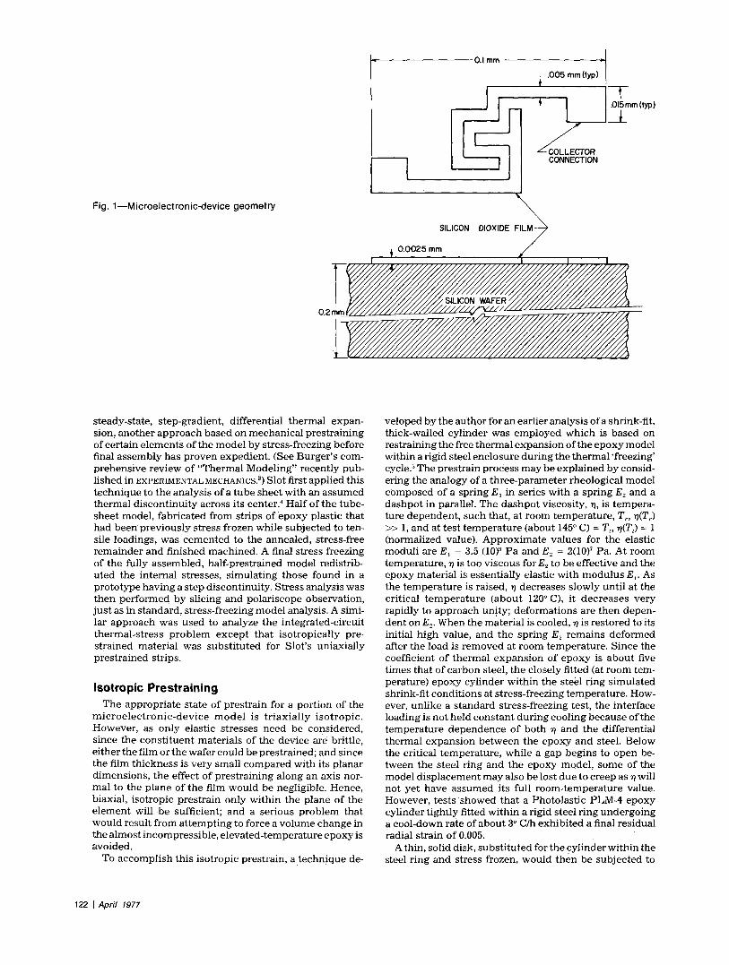
Fig. 1--Microelectronic-device geometry
0.1 mm 1 I .005 rnrn (typ)
I I 'yp)
0.2
steady-state, s tep-gradient , different ial the rmal expan- sion, another approach based on mechan ica l pres t ra in ing of cer ta in e l emen t s of the mode l by stress-freezing before final a s sembly has p roven expedient . (See Burger ' s com- p rehens ive r ev iew of "The rma l Model ing" recent ly pub- l ished in EXPERIMENTAL MECHANICS?) Slot first appl ied this t e c h n i q u e to the analysis of a tube sheet wi th an a s sumed thermal d i scont inu i ty across its center. 4 Hal f of the tube- sheet model , fabr icated f rom strips of e p o x y plastic that had been prev ious ly stress frozen whi le subjec ted to ten- sile loadings, was c e m e n t e d to the annealed, stress-free r ema inde r and f inished machined . A final stress freezing of the fully assembled, half-prestralned mode l redistrib- u ted the internal stresses, s imula t ing those found in a p ro to type hav ing a step discont inui ty . Stress analysis was then pe r fo rmed by sl icing and polar i scope observat ion, jus t as in s tandard, s tress-freezing mode l analysis. A simi- lar approach was used to analyze the in tegrated-ci rcui t thermal -s t ress p r o b l e m e x c e p t that i so t rop ica l ly pre- s t rained mater ia l was subs t i tu ted for Slot 's uniaxial ly pres t ra ined strips.
Isotropic Prestraining The appropr ia te state of pres t ra in for a por t ion of the
m i c r o e l e c t r o n i c - d e v i c e m o d e l is t r i ax i a l l y i so t rop ic . However , as only elastic s tresses need be considered, since the cons t i tuen t mater ia ls of the device are brittle, e i ther the film or the wafer could be prest ra ined; and since the film th ickness is ve ry small compared wi th its p lanar d imensions , the effect of pres t ra in ing along an axis nor- mal to the p lane of the film would be negligible. Hence, biaxial, i sotropic pres t ra in only wi th in the p lane of the e l emen t will be sufficient; and a serious p rob lem that would result f rom a t t empt ing to force a v o l u m e change in the a lmos t incompress ib le , e l eva ted- tempera tu re epoxy is avoided.
To accompl i sh this i sot ropic prestrain, a t echn ique de-
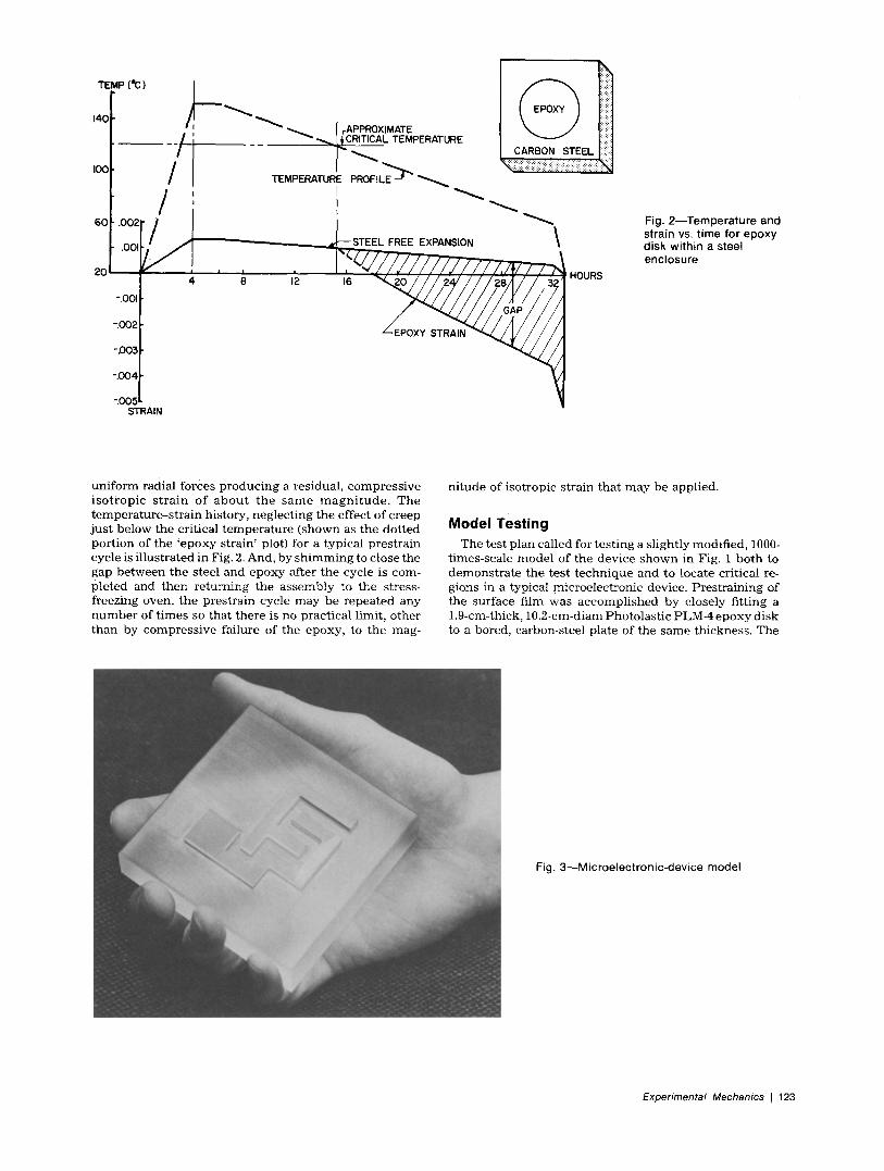
ve loped by the author for an earl ier analysis of a shrink-fit, th ick-wal led cy l inder was emp loyed which is based on restraining the free the rmal expans ion of the e p o x y mode l wi th in a rigid steel enc losure dur ing the the rmal ' f reezing' cycle2 The pres t ra in process may be exp la ined by consid- er ing the analogy of a th ree -paramete r rheologica l mode l composed of a spr ing E, in series wi th a spr ing E2 and a dashpot in parallel. The dashpot viscosi ty, 7, is tempera- ture dependent , such that, at room tempera tu re , Tr, ~(T,.) >> 1, and at test t empera tu re (about 145 ~ C) = T , ~?(T~) = 1 (normalized value). A p p r o x i m a t e va lues for the elastic modul i are E, = 3.5 (10) s Pa and E2 = 2(10) 7 Pa. At room tempera ture , ~ is too v iscous forE2 to be effect ive and the epoxy mater ia l is essent ia l ly elastic wi th modu lus E,. As the t empera tu re is raised, ~ decreases s lowly unt i l at the cri t ical t e m p e r a t u r e (about 120 ~ C), it dec rea se s ve ry rapidly to approach unity; deformat ions are then depen- dent onE2. When the mater ia l is cooled, ~? is res tored to its initial h igh value, and the spr ing E~ remains de fo rmed after the load is r emoved at room tempera ture . S ince the coefficient of thermal expans ion of epoxy is about five t imes that of carbon steel, the closely fitted (at room tem- perature) epoxy cyl inder wi th in the ste~l r ing s imula ted shrink-fit condi t ions at s t ress-freezing tempera ture . How- ever, un l ike a s tandard s tress-freezing test, the interface loading is not he ld cons tan t dur ing cool ing because of the t empera tu re d e p e n d e n c e of both ~ and the differential thermal expans ion be tween the epoxy and steel. Below the critical tempera ture , whi le a gap begins to open be- tween the steel r ing and the epoxy model , some of the mode l d i sp lacement may also be lost due to creep as ~ will not yet have as sumed its full room- tempera tu re value. However , tests s h o w e d that a Photolas t ic PLM-4 epoxy cyl inder t ight ly fitted wi th in a rigid steel r ing undergo ing a cool -down rate of about 3 ~ C/h exh ib i t ed a final residual radial strain of 0.005.
A thin, solid disk, subs t i tu ted for the cyl inder wi th in the steel r ing and stress frozen, would then be subjec ted to
122 I Apri l 1977
TEMP (~C)
140
I00
• / • ' \ \ \ \ ~,CRITICAL TEMPERATURE
, rAPPROXIMATE - / - - F ~ CARBON STEEL
PROFILE~ ~i::i::iiii!::i::i::iii::::::::::::i::i::i!::::i::i::i::i::i::i::iii:: ::i::;~::~::i ::ii ii:i TEMPERATURE
/ 60 ,002 / ~ i ~
,001
20 4 8 ,2 ,6 . . . . "~S//~/3, HOURS o o
-.002
-.005 i -.004
-.005 ! STRAIN
Fig. 2--Temperature and strain vs. time for epoxy disk within a steel enclosure
uni form radial forces p roduc ing a residual , compres s ive i s o t r o p i c s t r a in o f a b o u t t h e s a m e m a g n i t u d e . T h e t empera tu re - s t r a in history, neg lec t ing the effect of creep jus t below the cri t ical t empera tu re (shown as the do t ted por t ion of the ' epoxy strain' plot) for a typical pres t ra in cycle is i l lustrated in Fig. 2. And, by s h i m m i n g to close the gap be tween the steel and epoxy after the cycle is com- ple ted and then re tu rn ing the a s sembly to the stress- f reezing oven, the prestrain cycle may be repea ted any n u m b e r of t imes so that there is no pract ical l imit, o ther than by compress ive fai lure of the epoxy, to the mag-
n i tude of isotropic strain that may be applied.
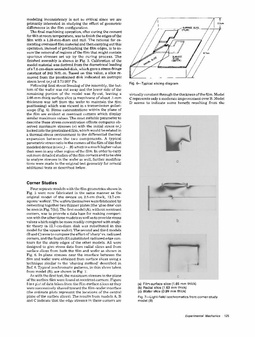
Model Testing The test p lan called for tes t ing a s l ightly modif ied, 1000-
t imes-scale mode l of the dev ice shown in Fig. 1 both to demons t r a t e the tes t t e c h n i q u e and to locate cri t ical re- gions in a typical microelec t ronic device. Pres t ra in ing of the surface film was accompl i shed by closely fit t ing a 1.9-cm-thick, 10.2-cm-diam Photo las t ic PLM-4 epoxy disk to a bored, carbon-steel plate of the same thickness. The
Fig. 3~Microelectronic-device model
Experimental Mechanics I 123

Fig. 4--Light- f ie ld isochromatics in f i lm
m o d e l film mater ia l was pres t ra ined a total of four t imes by adding addi t iona l s h i m m i n g after each heat ing cyclel Observa t ion of the p lane o f the disk after pres t ra in re- vea led the e x p e c t e d zero-order in te r fe rence eve rywhere excep t in small regions near the s t ee l - epoxy interface (this affected mater ia l was discarded): After final pre- straining, the disk was twice sl iced parallel to its surface to p roduce three th in disks. The central d isk was then fly-cut top and bot tom to 0.25-cm thickness , roughly cut to the out l ine of the film g e o m e t r y and c e m e n t e d to a p rev ious ly f inished l l .4 -cm-square , 2.5-cm-thick wafer of the an-
nealed, stress-free mater ia l wi th Tra-Con 2101 epoxy ce- ment. I f the wafer th ickness were kep t to t rue scale, it would need to be ten t imes this th ickness ; however , by using a mode led film to wafer th ickness ratio of 10, it was clearly seen that the in ter face d i s tu rbance did not propa- gate to the bo t tom of the wafer [ e.g., see Fig. 7(b)]. Both the mode l ed film and wafer were fabr icated f rom the same epoxy sheet. This impl ies that the modu lus of elast ici ty of silicon and si l icon d iox ide are very similar. In poin t of fact, the modu lus of elast ici ty of si l icon is 1.6 (10)" Pa and the modu lus of si l icon d iox ide is 7 (10) ~~ Pa. However , this
NOTE: ALL DIMENSIONS IN cm
A B
f b,,,• T,,8
.08R-
.25 v / / / / / / / / A - - ] L
SECT X-X Fig. 5---Film conf igurat ions for corner-study models
C D 5,59 ~ .:~5 .z5
i l ,..: __,.
~" .25 ~ 2 5
SECT Y-Y
124 I April 1977
m o d e l i n g i n c o n s i s t e n c y is no t so cr i t ical s ince we are p r imar i ly i n t e r e s t e d in s t u d y i n g t he e f fec t of g e o m e t r i c d i f fe rences in t he fi lm conf igura t ion .
The final m a c h i n i n g opera t ion , af ter cu r ing t he c e m e n t for 48 h at r o o m t e m p e r a t u r e , was to f in ish t he edges of the film wi th a 1 .59-mm-diam e n d mill. T h e ra t iona l for ce- m e n t i n g overs ized film ma te r i a l and t h e n ca r ry ing o u t th i s opera t ion , i n s t e a d of p r e f i n i s h i n g t he fi lm edges , is to in- sure t h e r e m o v a l of r eg ions of t he fi lm t h a t m i g h t c o n t a i n s p u r i o u s s t r e s s e s se t u p b y t h e c u r i n g p r o c e s s . T h e f in i shed a s s e m b l y is s h o w n in Fig. 3. Ca l i b r a t i o n of t h e m o d e l ma te r i a l was de r i ved f rom the d i a m e t r i c a l l o ad i n g of a 7 .6-cm-diam a n n e a l e d disk, w h i c h gave a s t ress - f r inge c o n s t a n t of 345 N/fr.-m. B a s e d on t h i s va lue , a sl ice re- m o v e d f rom the p r e s t r a i n e d d i sk i n d i c a t e d a n i so t rop ic s t ress level (~o) of 5.71(10) ~ Pa.
Fo l lowing final s t ress f reez ing of t he a s s e m b l y , t h e bot- t om of t he wafe r was cu t away and t he lower s ide of the r e m a i n i n g p o r t i o n of t he m o d e l was fly-cut, l eav ing a 2 .66-ram-thick sur face sl ice (a m e m b r a n e of a b o u t . l - r am t h i c k n e s s was left f r om the wafer to m a i n t a i n t h e film pos i t ion ing) w h i c h was v i e w e d in a t r a n s m i s s i o n polar i - scope (Fig. 4). S t re s s c o n c e n t r a t i o n s w i t h i n t he p l a n e of the film are e v i d e n t at r e e n t r a n t co rne r s w h i c h d i sp lay s imi lar m a x i m u m values . The m o s t su i t ab l e p a r a m e t e r to desc r ibe t h e s e s t r e s s - c o n c e n t r a t i o n ef fec ts c o m p a r e s ob- se rved m a x i m u m s t resses (~) wi th t h e in i t ia l s t r e s s (~ro) locked in to t he p r e s t r a i n e d film, w h i c h w o u l d b e r e l a t ed in a t h e r m a l - s t r e s s e n v i r o n m e n t to the d i f fe ren t i a l t h e r m a l e x p a n s i o n b e t w e e n t h e t w o c o m p o n e n t s . A t y p i c a l p a r a m e t r i c s t ress rat io in t he corners of t he fi lm of t h i s first m o d e l e d dev ice is (~r/~o) = .95 w h i c h is a m u c h h i g h e r va lue t h a n seen in any o the r r eg ion of the film. In o rde r to car ry ou t more de ta i l ed s tud ies of the film co rne r s a n d to be ab le to analyze s t r e s ses in t he wafer as well, f u r t h e r modif ica- t ions were m a d e to t h e or ig ina l t e s t g e o m e t r y for severa l add i t iona l t e s t s as d e s c r i b e d below.
~ . T c m
Fig. 6--Typical slicing diagram
vi r tua l ly c o n s t a n t t h r o u g h t h e t h i c k n e s s of t h e film. Mode l C r e p r e s e n t s on ly a m o d e r a t e i m p r o v e m e n t ove r B. Mode l D s e e m s to i n d i c a t e s o m e b en e f i t r e s u l t i n g f r o m the
Corner Studies Four s epa ra t e m o d e l s w i t h the film g e o m e t r i e s s h o w n in
Fig. 5 were n o w fab r i ca t ed in the s a m e m a n n e r as t h e or iginal m o d e l of t he dev ice on 2.5-cm-thick, 12.7-cm- square 'wafers ' . The wafers t h e m s e l v e s were f a b r i c a t e d by c e m e n t i n g t o g e t h e r two t h i n n e r p la tes [ the 'g lue- l ine ' can be seen in Fig. 7(b)]. The first mode l (A), w i t h o u t r e e n t r a n t corners , was to p r o v i d e a da ta base for m a k i n g compar i - son wi th the o t h e r t h r e e m o d e l s as wel l as to p r o v i d e s t ress va lues w h i c h m i g h t be m o r e readi ly c o m p a r e d w i t h analy- tic t heo ry (a 12.7-cm-diam d isk was s u b s t i t u t e d in th i s mode l for the s q u a r e wafer). The s e c o n d a n d t h i r d m o d e l s (B and C) were to c o m p a r e the effect o f ' s h a r p ' vs. r a d i u s e d corners , and t he fou r th (D) s u b s t i t u t e d r a d i u s e d edge con- tours for t he s h a r p edges of the o t h e r mode l s . All were des igned to give s t ress da ta f rom rad ia l s l ices a n d f rom surface sl ices f rom b o t h t he film and wafe r as s h o w n in Fig. 6. In -p l ane s t resses n e a r the in te r face b e t w e e n the film and wafe r were o b t a i n e d f rom sur face s l ices u s i n g a t e c h n i q u e s imi la r to t he ' s h a v i n g m e t h o d ' d e s c r i b e d in Ref. 6. Typica l i s o c h r o m a t i c pa t te rns , in t h i n s l ices t a k e n f rom mode l (B), are s h o w n in Fig. 7.
As wi th t h e first test , t h e m a x i m u m s t re s ses in the p l ane of the sur face film were f o u n d at r e e n t r a n t corners . F igu re 8 is a plot of da ta t a k e n f rom the f i lm-surface s l ices as they were success ive ly s h a v e d t o w a r d the f i lm-wafe r in t e r face (the o rd ina t e p lo ts r e p r e s e n t the loca t ions of t he cen t ra l p lane of the sur face slices). The resu l t s f rom m o d e l s A, B and C ind ica t e t h a t the edge s t resses in t h e s e co r n e r s are
(a) Film-surface slice (1.65 mm thick) (b) Radial slice (1.63 mm thick) (c) Wafer slice (0.99 mm thick)
Fig. 7--Light-field isochromatics from corner-study model (B)
Experimental Mechanics I 125

radiused-edge contour . B u t this effect is main ly due to the plot ted values be ing t aken at the edge of the newly shaved film surface which is m o v i n g in an ou tward d i rec t ion as the shaving of the slices approaches the in ter face and not at the initial film edge; hence , the lower p lo t ted va lues occur in the fea thered-edge region.
Radial slices, t aken across the inner and ou te r corners, gave data to reveal m a x i m u m shear s tresses in t h e film and wafer and a l lowed two general observa t ions to be made: first, that the pat terns of shearing stress in the region of the outer corners of the film were about twice as act ive as those near the reen t ran t corners; and second, that the m a x i m u m s h e a r s t r e s s e s are v e r y h i g h l y l oca l i zed . M a x i m u m fr inge orders could be read in a t ransmiss ion polar i scope us ing Tardy compensa t ion only wi th the aid of a 20-power m i c r o s c o p e . E x c e p t for m o d e l D, the m a x i m u m shear stress in the wafers occurs ve ry near the surface jus t at the edge of the film (see Fig. 9). The stress ratios repor ted in Fig. 9 are based on compar ing these stresses (rmax) wi th the init ial film pres t ra in m a x i m u m shear stress which, s ince one of the pr incipal s t resses in the p r e s t r a l n e d d i s k is zero, is equa l to 1/2 ~o; hence , the parametr ic stress ratio is t aken as 2r~,ax/~o. F igure 9 shows that the range of m a x i m u m shear stresses in all the mod- els was not ve ry great. The lower stresses in the wafers of mode ls B-D m a y be due to a more localized shear concen- t ra t ion in the v ic in i ty of a corner compared to the more uniform, a lmos t plane-s t ra in field of mode l A. Fur ther - more, it is possible that more highly stressed, local points in the films were not obse rved because the f i lm-corner angle isn ' t normal to the p lane of the slice. [See, for example , the film edge in F igure 7(b); these anomalous regions are indi- ca ted by the heavy, dark film boundar ies in Fig. 9]. Sur- face slices taken a long the top of the wafer [as in F igure 7(c)] served to indica te regions of m a x i m u m shear in the p lane of the surface layer, but they did not o therwise pro- v i d e u s e f u l q u a n t i t a t i v e da ta b e c a u s e o f t h e h i g h l y localized shear-stress concen t ra t ions r ight at the interface surface.
S t r e s s e s f r o m m o d e l A w e r e also c o m p a r e d w i t h stresses p r ed i c t ed by modi f ied T i m o s h e n k o (uniaxial) theory of a b imeta l l ic str ip to ver i fy the mode l ing ap- proach. ~ As no ted by Burge r (Ref. 3, p. 432), for comple te biaxial restraint , the stress is 1/(1 - v) t imes greater than for the uniaxia l case. This t e r m was added to t h e Timo- shenko equa t ions giving:
N tlEi ( 1 - v ) m = t -~ + 2r (1)
N Elt~ + E=t~ (2) 6 hr
L0
0.9
0.8
0,7
0.6
0 . 5 I
0.4
O.3
02
OA
. . . . . . - _ 0 0 ~ 0
~MODEL B
~MODEL C
O s J
s S s ~
sO~'s%MODEL D f
f s S ~-'-MODEL A
. J . . . . o 9 " , o o
J , J o o12 0 6 Iio 14ram -~
Fig. 8~Stress-rat ios (o-/o-.) from" fi lm surface slices vs. locat ion of slice central plane above the f i lm-wafer interface
Fig. 9 - - M a x i m u m stress ratios at outside corners from radial slices
MODEL
A
LOCATION OF CONCENTRATION
~ LM
L MAX WAF!R / - MAX ,, FILM
~ ILM
L MAX.WAFER
FILM
1.35
1.22
1.24
1.25
2 TmoxlO-o
WAFER
1.25
I. I0
I,O4
1.03
126 I April 1977
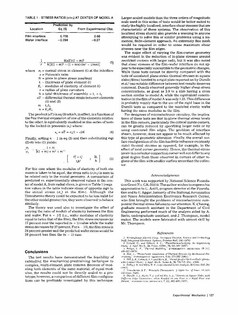
TABLE 1--STRESS RATIOS (o-/o-o) AT CENTER OF MODEL A
Prediction by Location Eq (5) From Experimental Obs.
Film interface 0.706 0.68 Wafer interface -0.294 -0.27
1 6(aT) (1 + m y r = h [3(1 + m) 2 + (1 + r a n ) ( m 2 + 1/mn)] (3)
w h e r e oq = n o r m a l s t ress in e l e m e n t (i) a t t he in t e r f ace = P o i s s o n ' s ra t io
N = p la te i n -p l ane s t ress r e s u l t a n t t, = t h i c k n e s s of p la te e l e m e n t (i)
E~ = m o d u l u s of e las t ic i ty of e l e m e n t (i) r = r ad ius of p la te c u r v a t u r e
'h = to ta l t h i c k n e s s of a s s e m b l y = t~ + t2 aT = d i f fe ren t i a l t h e r m a l s t ra in b e t w e e n e l e m e n t s
(1) a n d (2) m = tj/t~
n = Ej /E2
T h e p r o d u c t (aT) in eq (3) which , in effect, is a f u n c t i o n of the f ree t h e r m a l e x p a n s i o n of one of t he e l e m e n t s re la t ive to t he other , is e q u i v a l e n t l y m o d e l e d in th i s ser ies of t es t s b y t he locked- in p r e s t r a i n (e0) where :
eo = a T = (to(1 - u)/E (4)
Final ly , s e t t ing n = 1 in eq (3) and t h e n s u b s t i t u t i n g eqs (2)-(4) in to (1) yields:
m l + m (r,, 3(1 + m) + m ~ + m -~
t~ + t.~ + ~ ] (5) t ~h ~
For this case where the m o d u l u s of e last ic i ty of b o t h ele- m e n t s is t a k e n to be equal, t he s tress rat io (~r~/cro) is seen to be re la ted on ly to t he m o d e l geomet ry . A c o m p a r i s o n of p r ed i c t ed vs. e x p e r i m e n t a l l y o b s e r v e d va lues at the cen- ter of mode l A, f rom radia l slices, is g i v e n in Tab le 1 [nega- t ive va lues in the t ab le i nd i ca t e s t ress of oppos i t e s ign to t h e i n i t i a l s t r e s s ((%) in t h e f i lm] . A l t h o u g h t h e T i m o s h e n k o t h e o r y cou ld b e e x p e c t e d to be less va l id for t he o t h e r m o d e l geomet r i e s , t h e y we re o b s e r v e d to b e h a v e similar ly.
The t h e o r y was u s e d also to i nves t i ga t e t he ef fec t of va ry ing the ra t io of m o d u l i of e las t ic i ty b e t w e e n t h e film a n d wafer. Fo r n = 1/2 (i.e., wafer m o d u l u s of e las t ic i ty equa l to twice t h a t of t he film), t he fi lm s t r e s s i nc r ea se s by 17 p e r c e n t ove r t he r e p o r t e d (n = 1) va lue whi l e t he wafe r s t ress dec reases by 27 pe rcen t . F o r n = 1/3, t he fi lm s t ress is 24 p e r c e n t g rea te r a n d t he p r e d i c t e d wafe r s t ress w o u l d be 38 p e r c e n t less t h a n the (n = 1) case.
Conclusions The tes t r esu l t s h a v e d e m o n s t r a t e d t he feas ib i l i ty of
e x t e n d i n g t h e m e c h a n i c a l - p r e s t r a i n i n g t e c h n i q u e to complex , mu l t i - e l emen t , p la te sys tems . B e c a u s e of mod- e l ing b o t h e I e m e n t s of t he s ame mater ia l , of equa l mod- ulus , t he resu l t s cou ld no t be d i rec t ly sca led to a pro- to type; however , a c o m p a r i s o n of d i f f e ren t fi lm conf igura- t ions can be p rof i t ab ly i nves t i ga t ed b y th i s t e c h n i q u e .
Larger - sca led m o d e l s t h a n t h e t h r e e o r d e r s of m a g n i t u d e scale u s e d in t h i s ser ies of t e s t s w o u l d b e b e t t e r s u i t e d to s t u d y t h e h i g h l y local ized, i n t e r f ace s h e a r s t r e s se s t h a t are cha rac t e r i s t i c of t h e s e sys tems . T h e o b s e r v a t i o n of th i s local ized s t ress s h o u l d also p r o v i d e a w a r n i n g to a n y o n e a t t e m p t i n g to so lve th i s or s imi la r p r o b l e m s u s i n g a nu- merical , f in i te -e lement approach . A n e x t r e m e l y fine m e s h w o u l d b e r e q u i r e d in o rde r to s e n s e m a x i m u m s h e a r s t resses n e a r t h e fi lm edges .
T h e m a j o r e f fec t of v a r y i n g the f i lm-corne r g e o m e t r y was e v i d e n t in the r educ t i on of in -p lane s t resses a r o u n d r e e n t r a n t c o r n e r s w i t h l a rge r radii , b u t i t was a lso n o t e d t ha t s h e a r s t r e s se s a t t h e f i lm-wafe r i n t e r f a c e do n o t ap- p e a r to b e e spec ia l ly s u s c e p t i b l e to t h e g e o m e t r i c changes . While t h e s e t e s t s c a n n o t b e d i rec t ly c o m p a r e d w i t h t he tes ts of s i m u l a t e d p l ane - s t r a in t h e r m a l s t r e s ses in s q u a r e s labs [films] b o n d e d to a r ig id p la te r e p o r t e d on by Dure l l i et al, 8 one n o t a b l e d i f f e rence b e t w e e n t e s t r e su l t s d e s e r v e s c o m m e n t . Dure l l i o b s e r v e d genera l ly h i g h e r shea r - s t r e s s c o n c e n t r a t i o n s , as g rea t as 3.0 in a s lab h a v i n g a c ross sec t ion s imi la r to m o d e l A, whi l e t he e q u i v a l e n t c oncen - t r a t i on in t he f i lm of m o d e l A was on ly 1.35. Th i s d i f f e r ence is p r o b a b l y m a i n l y due to t he use of t h e r ig id b a s e in t he Durel l i t e s t s as c o m p a r e d to t he m o d e l e d e las t ic wafe r h a v i n g t he s a m e m o d u l u s as t he film.
Fo r d e s i g n e r s of m i c r o e l e c t r o n i c c i rcui t ry , t h e impl ica- t ions of t h e s e t e s t s are t h a t in -p lane t h e r m a l - s t r e s s leve ls in t he fi lm corners , pa r t i cu la r ly the cr i t ica l i n s ide corners , can b e g rea t ly r e d u c e d b y spec i fy ing l a rge r rad i i or by u s ing c o n t o u r e d film edges . The p r o b l e m of in t e r f ace shears , howeve r , does no t a p p e a r to be m u c h a f fec ted by th i s t y p e of g e o m e t r i c a l te ra t ion . F ina l ly , t he overa l l sur- face con f igu ra t i on of t he fi lm has l i t t le i n f luence on ( s teady state) t h e r m a l s t r e s ses as opposed , for e x a m p l e , to t he effect of local c o r n e r geomet ry . Hence , t he t h e r m a l - s t r e s s levels in a co l l ec to r c o n n e c t i o n c o r n e r wil l no t d i f fer to any grea t deg ree f rom those o b s e r v e d in co rne r s of o t h e r re- g ions of t he fi lm w i t h smal l e r sur face areas t h a n t he collec- tor.
A c k n o w l e d g m e n t s
This w o r k was s u p p o r t e d by N a t i o n a l Sd ience F o u n d a - t ion G r a n t No. GK-35510. The a u t h o r w i s h e s to e x p r e s s his a p p r e c i a t i o n to C. Astil l , p r o g r a m d i r e c t o r a t t he F o u n d a - t ion a n d to E. Apgar , fo rmer ly of t he N a t i o n a l A e r o n a u t i c s and S p a c e A d m i n i s t r a t i o n E lec t ron i c s R e s e a r c h Cente r , w h o first b r o u g h t the p r o b l e m s of m i c r o e l e c t r o n i c com- p o n e n t t h e r m a l s t r e s s fa i lures to ou r a t t en t ion . K. C h e u n g , g r adua t e r e sea rch as s i s t an t in t he D e p a r t m e n t of Civil Eng inee r i ng p e r f o r m e d m u c h of t he analys is a ided b y A. Szeto, u n d e r g r a d u a t e ass i s tan t , and J, T h o m p s o n , m o d e l maker . The m o d e l s were f ab r i ca t ed w i t h u t m o s t skil l by Mr. T h o m p s o n .
R e f e r e n c e s
1. Westinghouse Electric Corp., Aerospace Division, Science and Technology Staff, Integrated Electronic Systems, Prentice-Hall, 396 (1,970).
2. Gerard, G., and Gilbert, A. C., "Photothermoelastieity: An Exploratory Study,-J. Appl. Mech., 24, Trans. ASME, 7,9, 355-360 (1,957).
3. Burger, C. P., "'Thermal Modeling," EXPERIMENTAL MECt-IANICS, 15 (11), 430-442 (1,975).
4. Slot, T., -Photoelastic Simulation of Thermal Stresses by Mechanical Pre- straining," EXI'ERIMI~;NqAL MECHANICS, 5 (,9), 273-282 (1,965).
5. Hill, L. R., Cakmak, A. S. and Mark, R., "Shrink-fit of a Thick-walled Cylinder with Contact Shear, 'J. Appl. Mech., Series E, 35, 729-736 (Dec. 1,968).
6. Dally,J. W. and Riley, W. F., Experimental Stress Analysis, McGraw-Hill, 266 (1965).
7. Timoshenko, S. P., "'Bimetalic Thermostats,"J. Optic Soc. uf Arner., 11, 233- 255 (Sept. 1'925).
8. DureUi, A. J., Parks, V. J. and del Rio, C. J., "'Stresses in Square Slabs, with Different Edge Geometries, when Bonded on one Face to a Rigid Plate and Shrunk," EXPEIalXJ~:NTAL M~CH.r 7 (11), 482-484 (1,967).
Experimental Mechanics I 127