Embed Size (px)
Citation preview
Photodetectors
Course: Consumer Optoelectronics (EE594)
Sang Kyu Kwak
2
Contents
• Overview• Concept of Photodetectors• Types and Applications
– Forcus on semiconductor photodetectors
• Recent Technology of Photodetectors• References
3
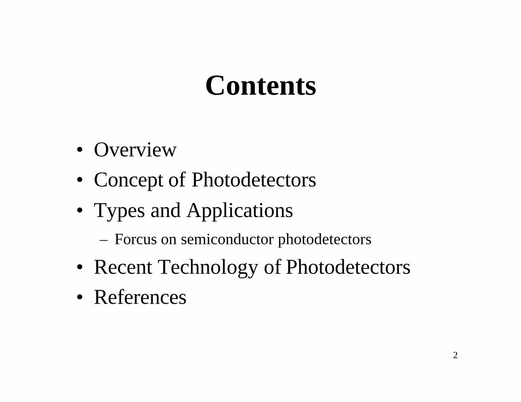
Overview
* ref.: http://hyperphysics.phy-astr.gsu.edu/hbase/electronic/optelcon.html#c1
4
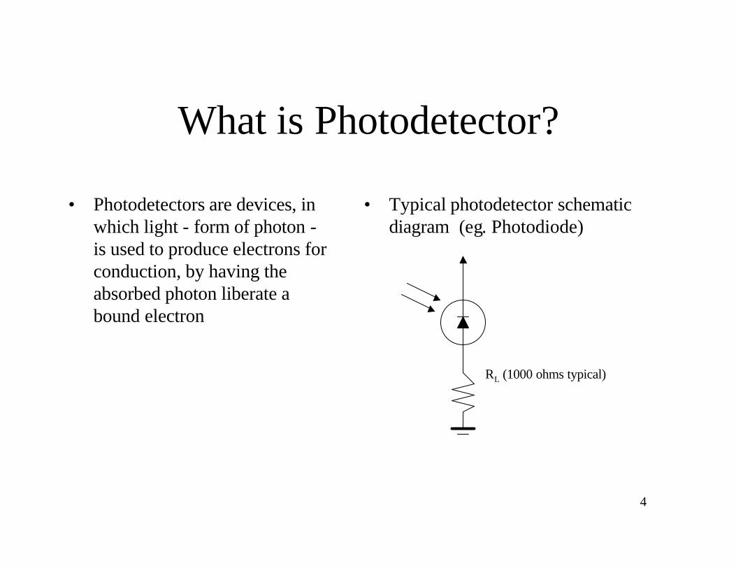
What is Photodetector?
• Photodetectors are devices, in which light - form of photon -is used to produce electrons for conduction, by having the absorbed photon liberate a bound electron
• Typical photodetector schematic diagram (eg. Photodiode)
RL (1000 ohms typical)
5
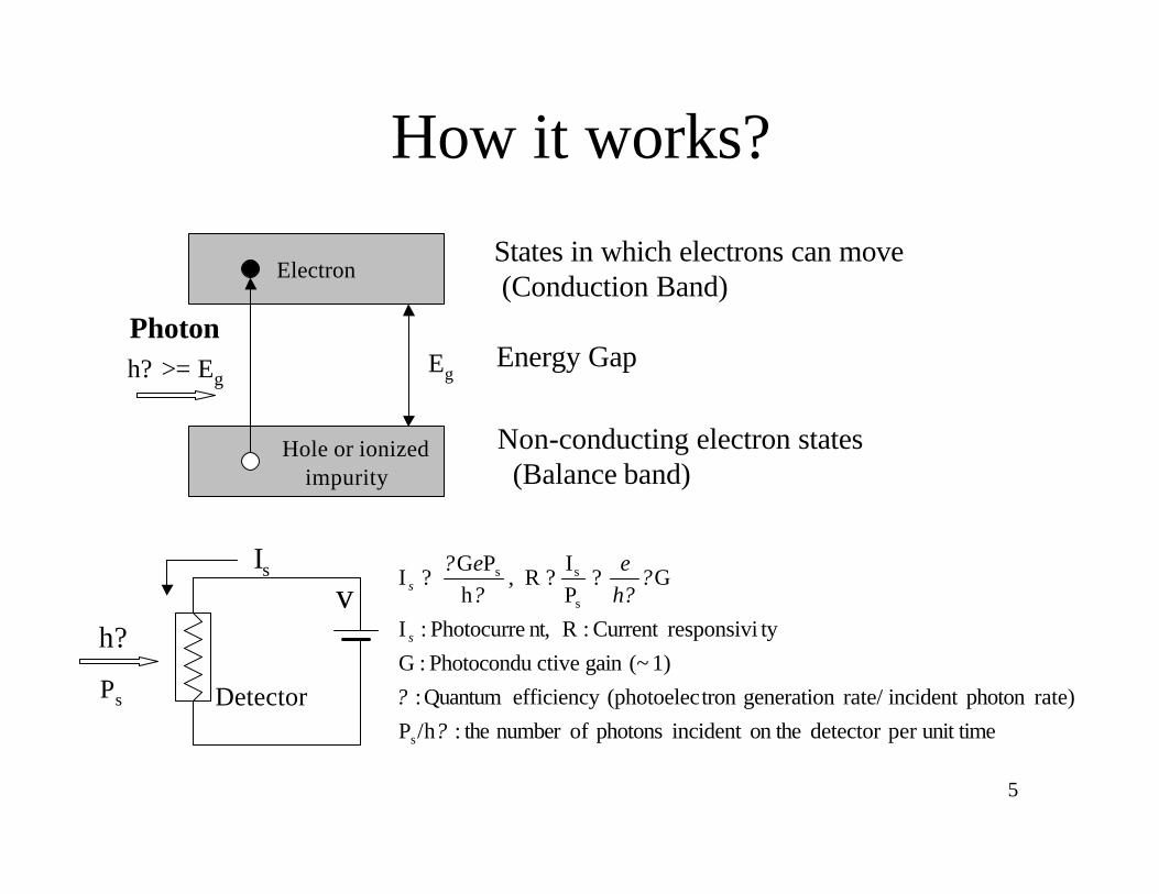
How it works?
Electron
Hole or ionizedimpurity
Photonh? >= Eg
EgEnergy Gap
States in which electrons can move(Conduction Band)
Non-conducting electron states(Balance band)
h?
Is
v
Detectorunit timeper detector on theincident photons ofnumber the:/hP
rate)photon incident rate/ generationtron (photoelec efficiency Quantum :1)(~gain ctivePhotocondu :G
tyresponsiviCurrent :R nt,Photocurre :I
GPI
R , h
PG I
s
s
ss
??
???
?
s
s hee
???
Ps
6
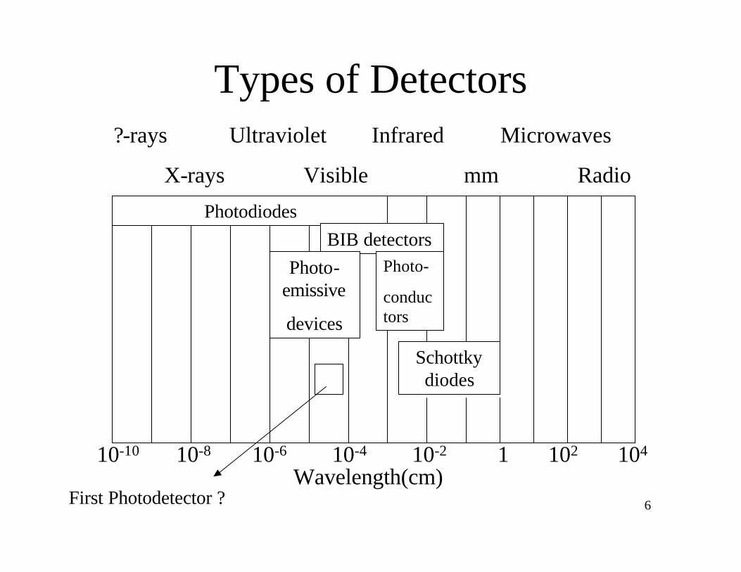
Types of Detectors?-rays Ultraviolet Infrared Microwaves
X-rays Visible mm Radio
10-10 10-8 10-6 10-4 10-2 1 102 104
Wavelength(cm)
PhotodiodesBIB detectors
Photo-
conductors
Photo-emissive
devices
Schottky diodes
First Photodetector ?
7
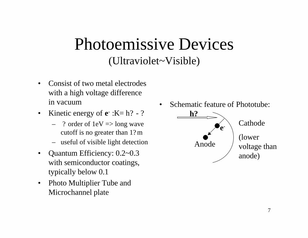
Photoemissive Devices (Ultraviolet~Visible)
• Consist of two metal electrodes with a high voltage difference in vacuum
• Kinetic energy of e- :K= h? - ?– ? order of 1eV => long wave
cutoff is no greater than 1? m– useful of visible light detection
• Quantum Efficiency: 0.2~0.3 with semiconductor coatings, typically below 0.1
• Photo Multiplier Tube andMicrochannel plate
• Schematic feature of Phototube:h?
e-
Anode
Cathode
(lower voltage than anode)
8
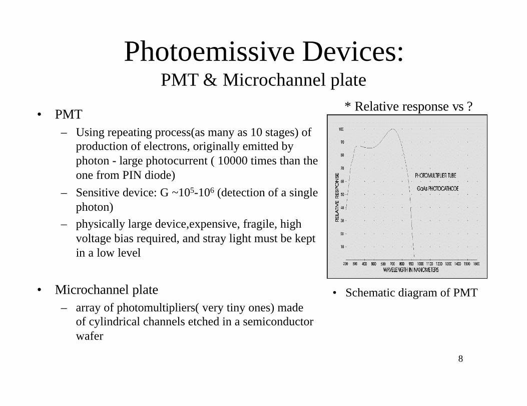
Photoemissive Devices:PMT & Microchannel plate
• PMT– Using repeating process(as many as 10 stages) of
production of electrons, originally emitted by photon - large photocurrent ( 10000 times than the one from PIN diode)
– Sensitive device: G ~105-106 (detection of a single photon)
– physically large device,expensive, fragile, high voltage bias required, and stray light must be kept in a low level
• Microchannel plate– array of photomultipliers( very tiny ones) made
of cylindrical channels etched in a semiconductor wafer
* Relative response vs ?
• Schematic diagram of PMT
9
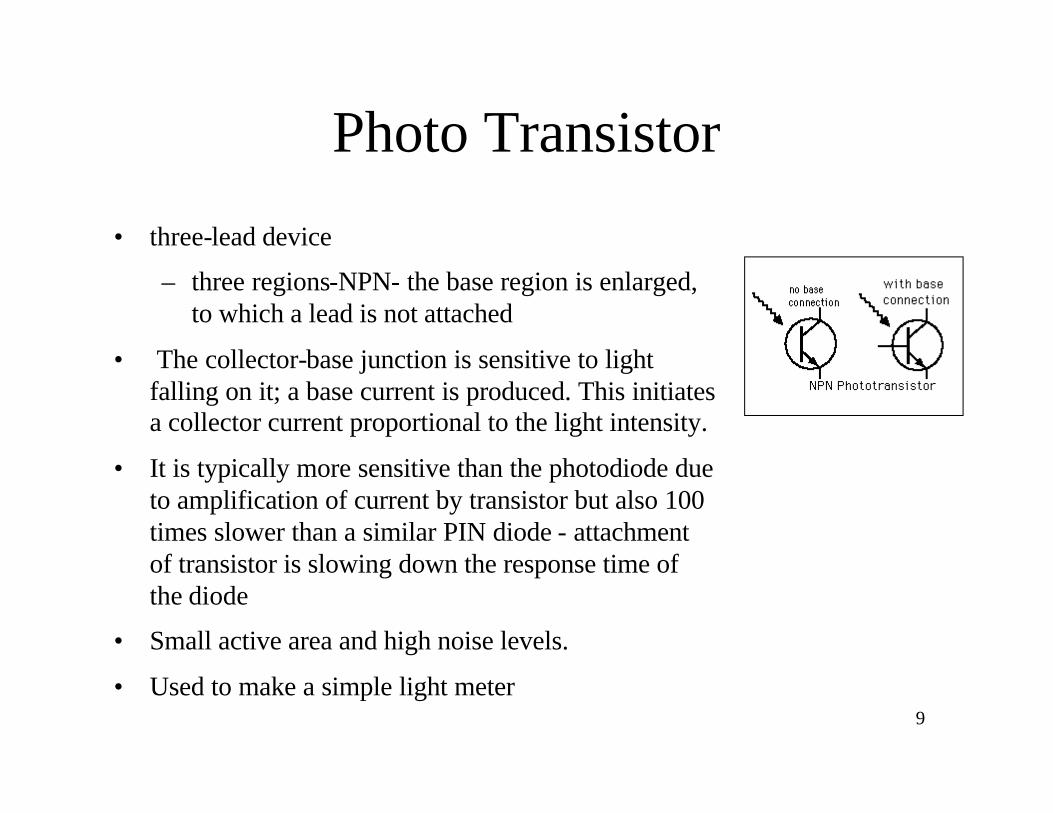
Photo Transistor
• three-lead device
– three regions-NPN- the base region is enlarged, to which a lead is not attached
• The collector-base junction is sensitive to light falling on it; a base current is produced. This initiates a collector current proportional to the light intensity.
• It is typically more sensitive than the photodiode due to amplification of current by transistor but also 100 times slower than a similar PIN diode - attachment of transistor is slowing down the response time of the diode
• Small active area and high noise levels.
• Used to make a simple light meter
10
Photo Resistors
• Low cost, two lead photoresistors using a cadmium sulfide (CdS) element show a dramatic decrease in resistance when illuminated and are commonly used as a light sensing element for security lights, etc. so that they will turn on at night.
• In the dark, the resistance is very high, in the 1 megohm range. When illuminated, the resistance may drop to a few hundred ohms. They are typically more sensitive to green light, and they have a very high sensitivity compared to other types of sensors.
• Not practical for high speed switching or modulation for communications purposes due to a memory effect, requiring on the
order of a second for the resistance to rise to its dark resistance.
11
• Simplest semiconductor detectors• Intrinsic and Extrinsic Semiconductors
– Periodic Table
• Consist of conduction and balance band• Quantum efficiency: as high as 0.7 for short-wavelength,
usually 0.2~0.4
Photoconductors (Infrared)
12
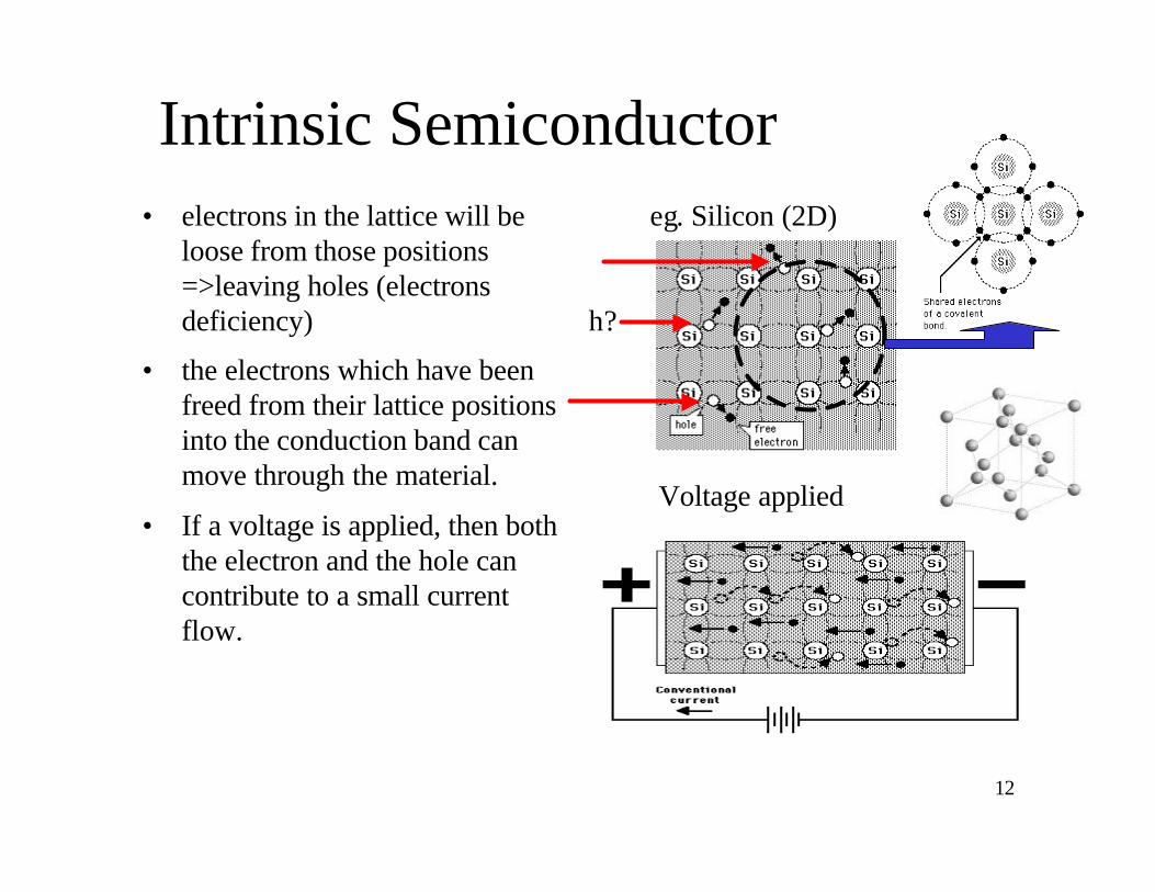
Intrinsic Semiconductor• electrons in the lattice will be
loose from those positions =>leaving holes (electrons deficiency)
• the electrons which have been freed from their lattice positions into the conduction band can move through the material.
• If a voltage is applied, then both the electron and the hole can contribute to a small current flow.
h?
Voltage applied
eg. Silicon (2D)
13
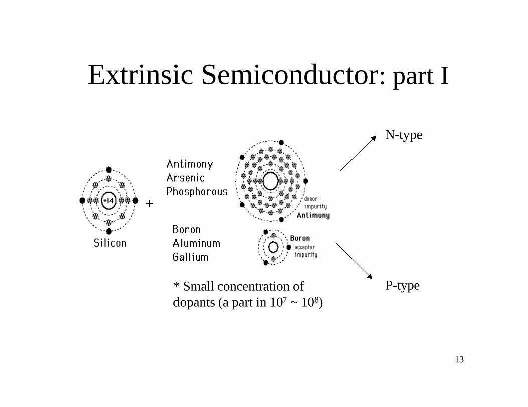
Extrinsic Semiconductor: part I
+
N-type
P-type* Small concentration of dopants (a part in 107 ~ 108)
14
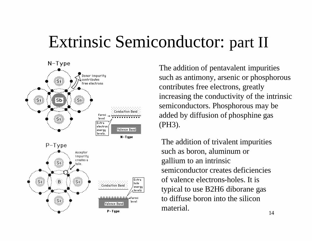
Extrinsic Semiconductor: part IIThe addition of pentavalent impurities such as antimony, arsenic or phosphorous contributes free electrons, greatly increasing the conductivity of the intrinsic semiconductors. Phosphorous may be added by diffusion of phosphine gas (PH3).
The addition of trivalent impurities such as boron, aluminum or gallium to an intrinsic semiconductor creates deficiencies of valence electrons-holes. It is typical to use B2H6 diborane gas to diffuse boron into the silicon material.
15
Intrinsic and Extrinsic semiconductors
• Due to band gap and impurity ionization potential => a long-wavelength threshold for photoresponse
• Energy producing carriers are quite small => need to operate at very low (cryogenic) temperature by a rule kBT<< Eg
• the longer the threshold wavelength, the colder they needed to be– Si extrinsic PCs: T~4-10K– Ge extrinsic PCs (eg. Ge:Ga): T~<4K
* Stressed Ge:Ga works best at T=1.3-1.4K
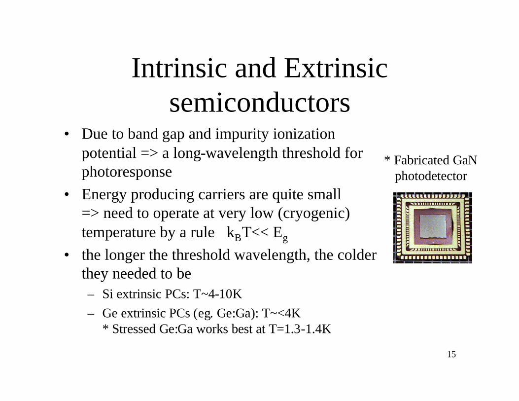
* Fabricated GaN photodetector
16
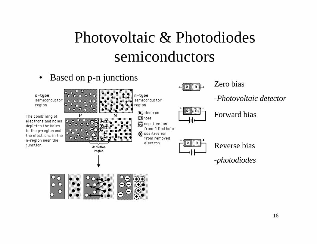
Photovoltaic & Photodiodes semiconductors
• Based on p-n junctionsZero bias
-Photovoltaic detector
Forward bias
Reverse bias
-photodiodes
17
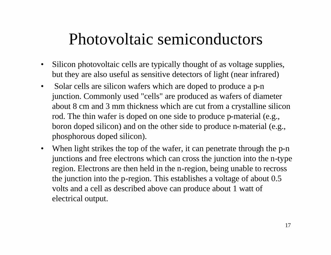
Photovoltaic semiconductors• Silicon photovoltaic cells are typically thought of as voltage supplies,
but they are also useful as sensitive detectors of light (near infrared)• Solar cells are silicon wafers which are doped to produce a p-n
junction. Commonly used "cells" are produced as wafers of diameter about 8 cm and 3 mm thickness which are cut from a crystalline silicon rod. The thin wafer is doped on one side to produce p-material (e.g., boron doped silicon) and on the other side to produce n-material (e.g., phosphorous doped silicon).
• When light strikes the top of the wafer, it can penetrate through the p-n junctions and free electrons which can cross the junction into the n-type region. Electrons are then held in the n-region, being unable to recrossthe junction into the p-region. This establishes a voltage of about 0.5 volts and a cell as described above can produce about 1 watt of electrical output.
18
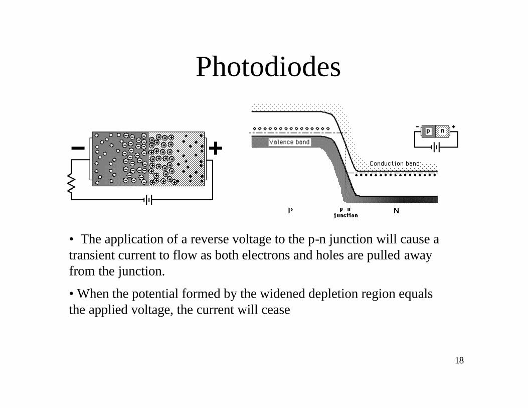
Photodiodes
• The application of a reverse voltage to the p-n junction will cause a transient current to flow as both electrons and holes are pulled away from the junction.
• When the potential formed by the widened depletion region equals the applied voltage, the current will cease
19
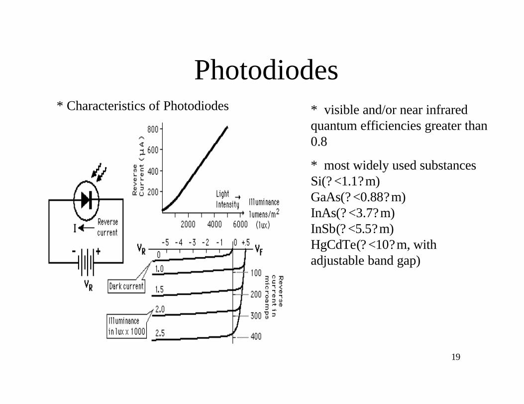
Photodiodes* visible and/or near infrared quantum efficiencies greater than 0.8
* most widely used substances Si(? <1.1?m) GaAs(? <0.88?m) InAs(? <3.7?m) InSb(? <5.5?m) HgCdTe(? <10?m, with adjustable band gap)
* Characteristics of Photodiodes
20
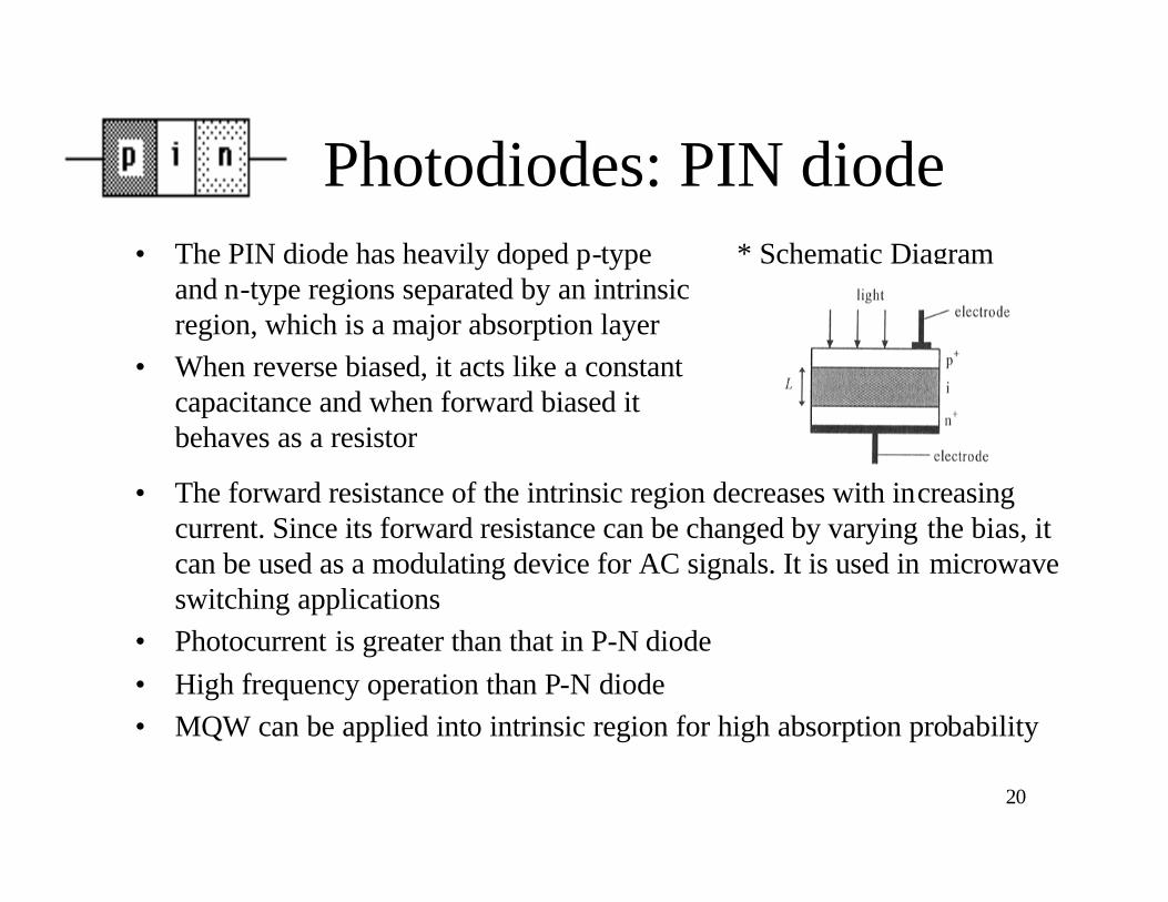
Photodiodes: PIN diode• The PIN diode has heavily doped p-type
and n-type regions separated by an intrinsic region, which is a major absorption layer
• When reverse biased, it acts like a constant capacitance and when forward biased it behaves as a resistor
• The forward resistance of the intrinsic region decreases with increasing current. Since its forward resistance can be changed by varying the bias, it can be used as a modulating device for AC signals. It is used in microwave switching applications
• Photocurrent is greater than that in P-N diode• High frequency operation than P-N diode• MQW can be applied into intrinsic region for high absorption probability
* Schematic Diagram
21
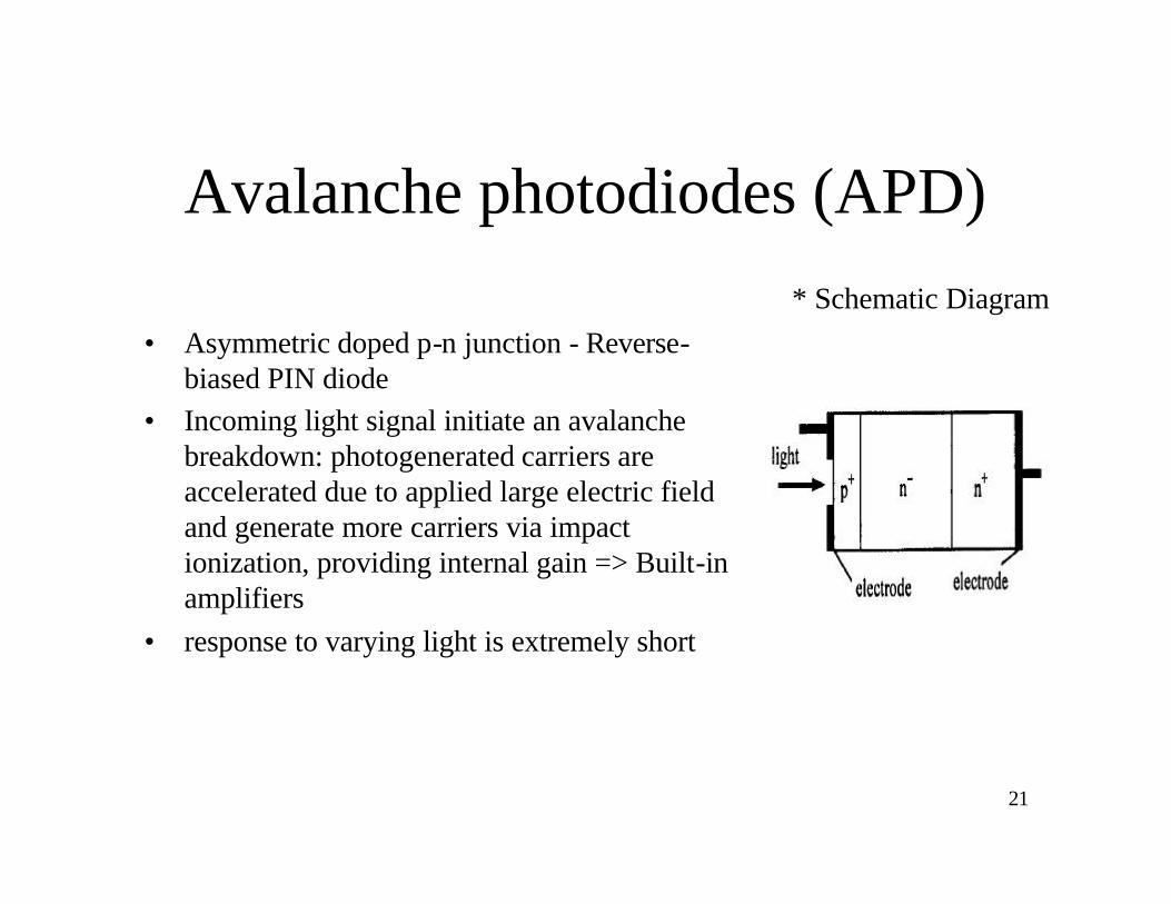
Avalanche photodiodes (APD)
• Asymmetric doped p-n junction - Reverse-biased PIN diode
• Incoming light signal initiate an avalanche breakdown: photogenerated carriers are accelerated due to applied large electric field and generate more carriers via impact ionization, providing internal gain => Built-in amplifiers
• response to varying light is extremely short
* Schematic Diagram
22
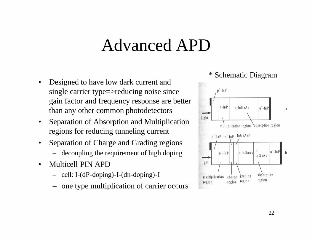
Advanced APD
• Designed to have low dark current and single carrier type=>reducing noise since gain factor and frequency response are better than any other common photodetectors
• Separation of Absorption and Multiplication regions for reducing tunneling current
• Separation of Charge and Grading regions– decoupling the requirement of high doping
• Multicell PIN APD– cell: I-(dP-doping)-I-(dn-doping)-I
– one type multiplication of carrier occurs
* Schematic Diagram
23
Photodiodes applications• Laser guided missiles, Laser warning , Laser range finders • Optical free air communication • Automotive anti collision optical radar • Laser alignment and control systems • Spectral analysis (medical ) • Two color sensor (combined with IR detector chip) • Monitoring of Hg lamps for sterilization • Film processing • Flame monitoring• Scintillator read out • Spectral monitoring of Earth ozone layer (environmental)
• Space applications (solar sensors, star sensors)
24
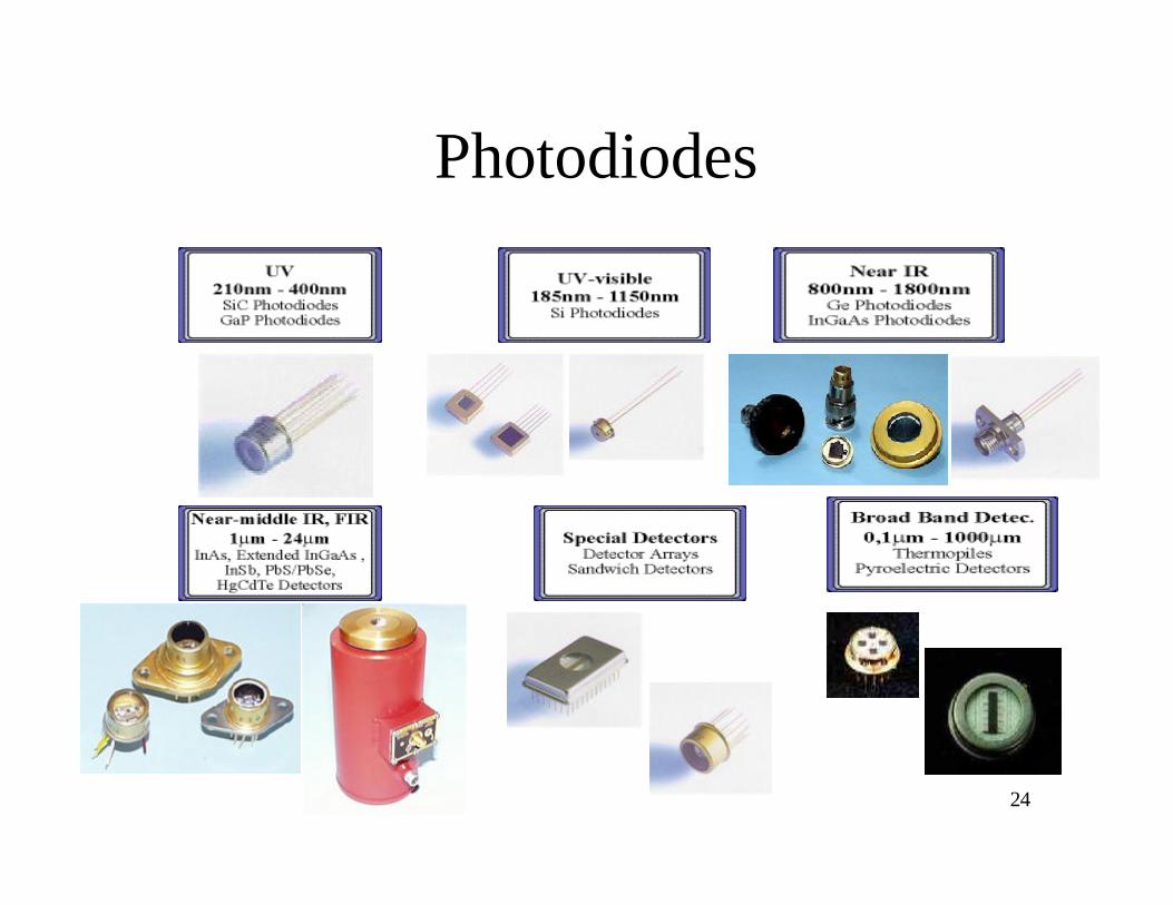
Photodiodes
25
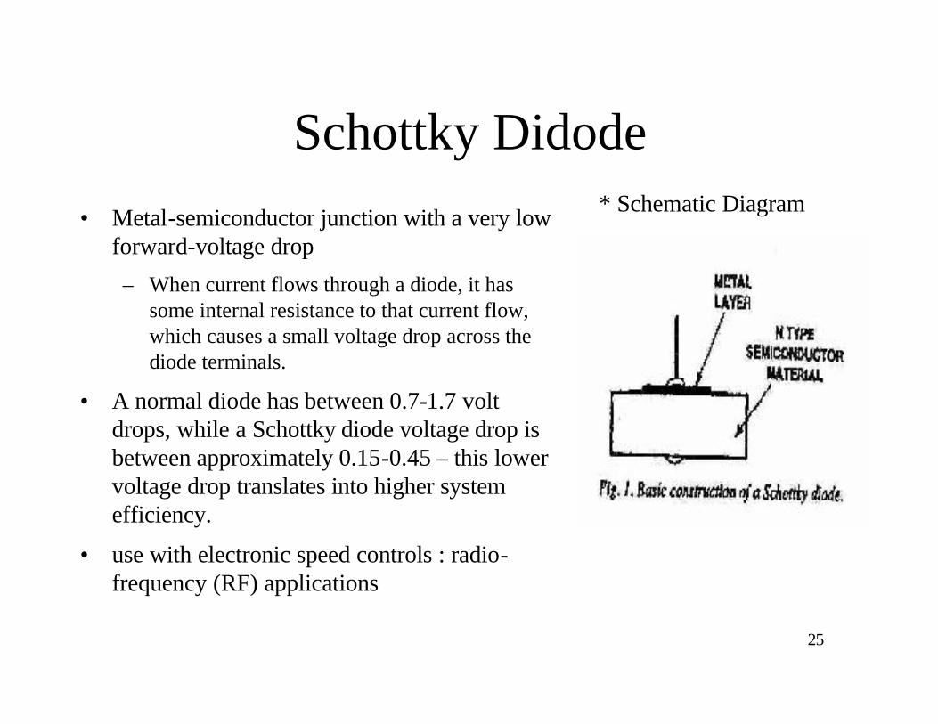
Schottky Didode• Metal-semiconductor junction with a very low
forward-voltage drop
– When current flows through a diode, it has some internal resistance to that current flow, which causes a small voltage drop across the diode terminals.
• A normal diode has between 0.7-1.7 volt drops, while a Schottky diode voltage drop is between approximately 0.15-0.45 – this lower voltage drop translates into higher system efficiency.
• use with electronic speed controls : radio-frequency (RF) applications
* Schematic Diagram
26
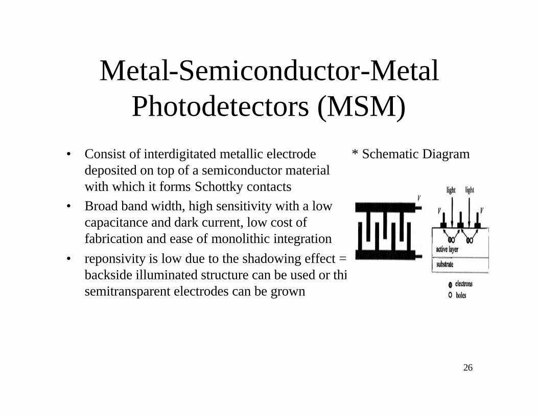
Metal-Semiconductor-Metal Photodetectors (MSM)
• Consist of interdigitated metallic electrode deposited on top of a semiconductor material with which it forms Schottky contacts
• Broad band width, high sensitivity with a low capacitance and dark current, low cost of fabrication and ease of monolithic integration
• reponsivity is low due to the shadowing effect => backside illuminated structure can be used or thin semitransparent electrodes can be grown
* Schematic Diagram
27
Other Photodetectors• Blocked-Impurity-Band detectors (BIB)
– low tunneling dark current for heavily doped and small volume detectors
• Wavelength Selective Photodetectors based on directional couplers– selects a desired wavelength from an incident light and spatially separates by
directional coupler
• Resonant Tunneling Photodetectors (RT)– resonant tunneling structure formed from AlAs barriers surrounding an
InGaAs QW, followed by a thick undoped InGaAs absorber layer on InP substrate: operates at low voltage, not sensitive to temp. changes
– high responsivity, gain-bandwidth efficiency, low switching energies
• Waveguide Photodetectors– side-illuminated waveguide (independently specifying the internal quantum
efficiency and the bandwidth)
• Traveling Wave Photodetectors (TW)– Waveguide Photodetectors whose electrode is supporting traveling electrical
waves with phase velocity matched to that of the external circuit– overcome RC bandwidth limitation of waveguide photodetectors
28
References• http://www.boselec.com/products/detmain.shtml• http://litec.rpi.edu/LITEC_Tutorial_3_7• http://www.semiseeknews.com/press_release2156.htm• http://www.mit-laser.cz/a/photodetectors.htm• http://www.electronicnews.com/enews/news/5734-349NewsDetail.asp• http://www.ame.no/• http://www.spie.org/web/journals/online/home.html• http://www.iis-b.fhg.de/de/jber99/proc_en.html• http://microelec.eng.morgan.edu/~web/photodetector.html• http://hyperphysics.phy-astr.gsu.edu/hbase/solids/diod.html#c3• http://www.multimania.com/jcviel/BTS/sujets/ELECTROTECH99.htm• Daniela Dragoman and Mircea Dragoman: " Advanced Optoelectronic Devices
"
• Astronomy 203 handouts, 1999 University of Rochester