Embed Size (px)
Citation preview
Department of Science and Technology Institutionen för teknik och naturvetenskap Linköpings Universitet Linköpings Universitet SE-601 74 Norrköping, Sweden 601 74 Norrköping
ExamensarbeteLITH-ITN-ED-EX--06/012--SE
Photochromic molecules inpolymer switch diodes
Feng-I Tai
2006-03-20

LITH-ITN-ED-EX--06/012--SE
Photochromic molecules inpolymer switch diodesExamensarbete utfört i Elektronikdesign
vid Linköpings Tekniska Högskola, CampusNorrköping
Feng-I Tai
Handledare xavier CrispinExaminator Xavier Crispin
Norrköping 2006-03-20

RapporttypReport category
Examensarbete B-uppsats C-uppsats D-uppsats
_ ________________
SpråkLanguage
Svenska/Swedish Engelska/English
_ ________________
TitelTitle
FörfattareAuthor
SammanfattningAbstract
ISBN_____________________________________________________ISRN_________________________________________________________________Serietitel och serienummer ISSNTitle of series, numbering ___________________________________
NyckelordKeyword
DatumDate
URL för elektronisk version
Avdelning, InstitutionDivision, Department
Institutionen för teknik och naturvetenskap
Department of Science and Technology
2006-03-20
x
x
LITH-ITN-ED-EX--06/012--SE
Photochromic molecules in polymer switch diodes
Feng-I Tai
Photochromism has been investigated extensively during recent years. The large interest for informationstorage in memory applications is associated with the bi-stable character of the photochromismphenomena.Here we first report the absorption spectra of solid-state films based on the blends consisting of PCmolecules, the spirooxazine1,3-dihydro-1,3,3-trimethylspiro[2H-indole-2,3�-[3H]phenanthr[9,10-b](1,4)oxazine] (PIII,Sigma-Aldrich, 32,256-3) and a polymer matrix host,poly(2-methoxy-5(2�-ethylhexyloxy)-1,4-phenylenevinylene) (MEH-PPV).Thereafter, the electricalperformance of PC-polymer diodes is characterized and reported. The retention time of the diode�s electrical switching fits quite well with the absorption characteristics ofthe blend films; this correspondence builds a good link between the film property and the devicebehavior. we observed a two-trap system in the blend diodes from the I-V curves, and a model is proposed whichcan explain the schematic concept of the trap-limited current modulation. We tested a novel device design based on a bi-layer of the PC and polymer materials, and the promisingresult for future work is presented in the end.
photochromic, polymer diodes, switchable traps
Upphovsrätt
Detta dokument hålls tillgängligt på Internet – eller dess framtida ersättare –under en längre tid från publiceringsdatum under förutsättning att inga extra-ordinära omständigheter uppstår.
Tillgång till dokumentet innebär tillstånd för var och en att läsa, ladda ner,skriva ut enstaka kopior för enskilt bruk och att använda det oförändrat förickekommersiell forskning och för undervisning. Överföring av upphovsrättenvid en senare tidpunkt kan inte upphäva detta tillstånd. All annan användning avdokumentet kräver upphovsmannens medgivande. För att garantera äktheten,säkerheten och tillgängligheten finns det lösningar av teknisk och administrativart.
Upphovsmannens ideella rätt innefattar rätt att bli nämnd som upphovsman iden omfattning som god sed kräver vid användning av dokumentet på ovanbeskrivna sätt samt skydd mot att dokumentet ändras eller presenteras i sådanform eller i sådant sammanhang som är kränkande för upphovsmannens litteräraeller konstnärliga anseende eller egenart.
För ytterligare information om Linköping University Electronic Press seförlagets hemsida http://www.ep.liu.se/
Copyright
The publishers will keep this document online on the Internet - or its possiblereplacement - for a considerable time from the date of publication barringexceptional circumstances.
The online availability of the document implies a permanent permission foranyone to read, to download, to print out single copies for your own use and touse it unchanged for any non-commercial research and educational purpose.Subsequent transfers of copyright cannot revoke this permission. All other usesof the document are conditional on the consent of the copyright owner. Thepublisher has taken technical and administrative measures to assure authenticity,security and accessibility.
According to intellectual property law the author has the right to bementioned when his/her work is accessed as described above and to be protectedagainst infringement.
For additional information about the Linköping University Electronic Pressand its procedures for publication and for assurance of document integrity,please refer to its WWW home page: http://www.ep.liu.se/
© Feng-I Tai
Photochromic molecules in polymer switch diodes
Abstract Photochromism has been investigated extensively during recent years. The large interest
for information storage in memory applications is associated with the bi-stable character of the
photochromism phenomena. In molecular photochromics, two isomers with different
absorption spectrum can be obtained according to the specific wavelength of the light
exposure. This reversible transformation process can be considered as optical writing/erasing
step of a memory.
Here we first report the absorption spectra of solid-state films based on the blends
consisting of PC molecules, the spirooxazine 1,3-dihydro-1,3,3-trimethylspiro[2H-indole-2,3’-
[3H]phenanthr[9,10-b](1,4)oxazine] (PIII, Sigma-Aldrich, 32,256-3) and a polymer matrix
host, poly(2-methoxy-5(2’-ethylhexyloxy)-1,4-phenylenevinylene) (MEH-PPV). The bi-
stability in conjugated polymer matrix is studied by following the time evolution of the optical
properties of the blends.
Thereafter, the electrical performance of PC-polymer diodes is characterized and reported.
While the PIII molecules in the blend bulks are switched to their low energy gap state,
forming external energy levels above the valence band of MEH-PPV, the injected charges
(hole-dominated) will be trapped by the low energy gap isomer of PIII and that leads to
current modulation. PIII molecules can be switched between two energy gap states upon the
photo-stimulation, and the I-V characteristics of the device can also be controlled reversibly
via the photoisomerization. The retention time of the diode’s electrical switching fits quite
well with the absorption characteristics of the blend films; this correspondence builds a good
link between the film property and the device behavior.
Furthermore, we observed a two-trap system in the blend diodes from the I-V curves, and
a model is proposed which can explain the schematic concept of the trap-limited current
modulation. To combine the knowledge and information from the investigations above, we
tested a novel device design based on a bi-layer of the PC and polymer materials, and the
promising result for future work is presented in the end.

1
Table of Contents 1 Introduction.......................................................................................................................... 3
1.1 Background ................................................................................................................. 3
1.2 Photochromism and photochromic molecules ............................................................ 4
1.3 Conjugated polymers .................................................................................................. 7
1.3.1 Basic structure.....................................................................................................7
1.3.2 Electronic properties ...........................................................................................8
1.4 Polymer diodes.......................................................................................................... 10
1.4.1 Basic concept ....................................................................................................10
1.4.2 Injection limited regime....................................................................................13
1.4.3 Space charge limited regime.............................................................................14
1.4.4 Trap filled limited regime .................................................................................15
1.5 Photochromic switch diodes ..................................................................................... 17
2 Materials and Goal............................................................................................................. 21
2.1 Photoisomerization ................................................................................................... 21
2.2 Goal........................................................................................................................... 24
3 Experimental techniques.................................................................................................... 24
3.1 Spincoating ............................................................................................................... 24
3.2 Profilometer .............................................................................................................. 26
3.3 Absorption spectroscopy........................................................................................... 27
3.3.1 UV-Vis absorption spectroscopy ......................................................................27
3.3.2 Spectrometer operating principle......................................................................29
3.4 Electrical measurements ........................................................................................... 30
4 Results and Discussion ...................................................................................................... 30
4.1 Photochromic molecules characterized by optical absorption measurements.......... 30
4.2 Time-dependent absorption spectra of the blends .................................................... 33
4.2.1 The solvent influence on photochromic switching ...........................................36
4.2.2 Annealing..........................................................................................................39
4.2.3 Thickness dependence ......................................................................................41
4.3 Switch diodes ............................................................................................................ 42

2
4.3.1 Basic understanding of MEH-PPV diodes........................................................43
4.3.2 The PIII/MEH-PPV switchable diodes.............................................................47
5 First steps towards a new architecture for the switch diodes............................................. 57
5.1 Absorption of PIII layer on top of MEH-PPV.......................................................... 57
5.2 First device data ........................................................................................................ 60
6 Conclusions........................................................................................................................ 62
7 References.......................................................................................................................... 64
8 Acknowledgement ............................................................................................................. 67

3
1 Introduction
1.1 Background
Organic semiconductors have been widely used in many electronic applications in recent
years, and tremendous efforts have been devoted to develop organic-based electronic devices
that can either compete with the traditional inorganic equivalents or add new functionalities
for (opto)electronic devices. Organic electronics can be manufactured from solution
processing, which has the potential to ensure inexpensive production costs [1]. In addition,
soluble organic molecular and/or polymeric materials make it possible to combine material
properties through solid-state blends or multilayered structures and achieve desired
characteristics. For instance, blends of organic semiconductors have allowed for the
improvement of electroluminescent quantum yield [2] and for improved control of bulk
charge transport in polymer diodes [3].
Among the new generation of “smart materials”, molecular switches are of increasing
interest to functionalize (opto)electronic devices. During the last decade, molecular switches
have been synthesized and employed into optoelectronic elements; for example memory cells
[4] and sensors [5]. A molecular switch is a molecule that can be switched between different
states with external stimulus, such as thermal energy, electrical stress, as well photon
excitation. Photochromic (PC) molecules represent one class of such molecular switches that
can be triggered by light irradiation. This kind of switching often relates to molecular
geometric rearrangement occurring as a consequence of a reversibly chemical process.
Photochromic molecules have been scrutinized for their potential applications in optical
storage [6, 7], electrical switch devices [8, 9], and as molecular wire switches [10, 11]. In
previous work, the device concept based on photochromic switch-diodes is presented; here
we report a special focus given from photochromic molecules blended with conjugated
polymers to build switchable diodes [12, 13].
4
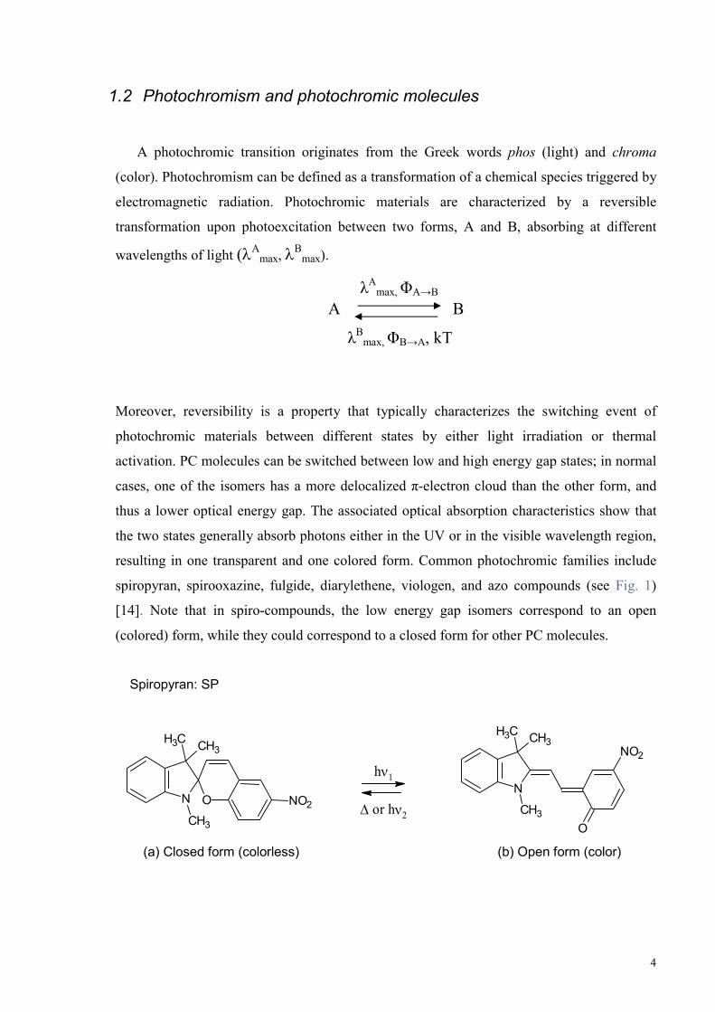
1.2 Photochromism and photochromic molecules
A photochromic transition originates from the Greek words phos (light) and chroma
(color). Photochromism can be defined as a transformation of a chemical species triggered by
electromagnetic radiation. Photochromic materials are characterized by a reversible
transformation upon photoexcitation between two forms, A and B, absorbing at different
wavelengths of light (λAmax, λB
max).
A B
Moreover, reversibility is a property that typically characterizes the switching event of
photochromic materials between different states by either light irradiation or thermal
activation. PC molecules can be switched between low and high energy gap states; in normal
cases, one of the isomers has a more delocalized π-electron cloud than the other form, and
thus a lower optical energy gap. The associated optical absorption characteristics show that
the two states generally absorb photons either in the UV or in the visible wavelength region,
resulting in one transparent and one colored form. Common photochromic families include
spiropyran, spirooxazine, fulgide, diarylethene, viologen, and azo compounds (see Fig. 1)
[14]. Note that in spiro-compounds, the low energy gap isomers correspond to an open
(colored) form, while they could correspond to a closed form for other PC molecules.
Spiropyran: SP
hν1
∆ or hν2
CH3 CH3
N
CH3
O NO2
CH3 CH3
N
CH3
NO2
O (a) Closed form (colorless) (b) Open form (color)
λAmax, ΦA→B
λB
max, ΦB→A, kT

5
Spirooxazine: C26H22N2O (PIII)
hν1
∆ or hν2
CH3 CH3
N
CH3
N
O
CH3 CH3
N
CH3
N
O
(a) Spiro form (colorless) (b) Planar form (color)
Fulgides
hν1
hν2
Me
O
MeO
O
MeMe
OMe
MeO
Me O
O
MeMe OMe
(a) Open form (colorless) (b) Closed form (color)
Diarylethenes
FFF
F
F
F
S
S
MeMe
FFF
F
F
F
S
SMe
Me
hν1
hν2
(a) Open form (colorless) (b) Closed form (color)

6
Azo-benzene
N Nhν1
hν2
N N
(a) Spiro form (colorless) (b) Planar form (color)
Figure 1: Chemical structures of prototypical photochromic molecules.
Typically, upon photoisomerization, the conjugated pathway (part of the molecule
including an alternation between double and single carbon-carbon bond) in the molecule is
modified. The longer the conjugated pathway, the smaller the HOMO-LUMO gap will be.
The structural modification in PC molecules is accompanied by an energy shift of the highest
occupied molecular orbital (HOMO) and/or of the lowest unoccupied molecular orbital
(LUMO). The photoisomerization, like any other chemical reaction, is sensitive to the
external conditions and the environment. Hence, the polarity of a matrix, its rigidity, and the
temperature are expected to have strong effects to the switching performance of PC
molecules. The most significant difference with respect to a liquid phase is that the
photochromic transition is much slower in the solid state.
Photochromic molecules are not yet commercially produced in optical storage or
electronic-switch elements because of their limitations to the technical requirements of such
devices:
Archive storage capability and (thermal) stability of both isomers
Low fatigue, i.e. the photochemical isomerization must be cycled many times
High sensitivity in a specific wavelength range and rapid response
Non-destructive readout capability
Among those requirements, the most important are the thermal stability and the fatigue
resistance. In general, photogenerated colored isomers are thermally unstable and return to

7
their initial structure spontaneously. Fatigue can be described as the loss of retention time,
which is due to chemical degradation. This loss limits the number of photochromic cycles
that the molecules can survive. The efficiency of the degradation routes depends on the
structure of the PC molecules. These switching properties require a lot of effort in research in
order to stabilize the metastable states [15]. To summarize this, most PC molecules can be
reversibly switched between two isomeric states upon light irradiation of specific optical
wavelengths. However, they can often be switched from their excited state by thermal
activation, which forces the PC molecules back to their initial isomeric ground state in
darkness and at room temperature, which is a crucial drawback in optoelectronic devices.
This class of photochromic molecules is classified as thermo-reversible to distinguish them
from the thermally stable but photo-reversible PC compounds.
1.3 Conjugated polymers
1.3.1 Basic structure
In 1977, Heeger, MacDiarmid and Shirakawa discovered that polyacetylene doped with
arsenic pentafluoride (AsF5) had its electrical conductivity increased up to the metallic
regime. For this discovery and their tremendous work on conjugated polymers, they were
awarded the Nobel Prize in chemistry. The π-conjugation in the polymer chain is due to the
alternating single (σ-bond) and double (π-bond) carbon-carbon bonds along the backbone
of the polymer chain. The 2pz atomic orbitals localized on each carbon overlap with
neighboring 2pz orbitals to create delocalized π-molecular orbitals. Electrons in π-orbitals
are delocalized over a certain spatial range. Due to the lack of intrinsic charge carriers, most
organic conjugated polymers are doped to achieve higher conductivity. Doping can be
either described by partial oxidation (p-doping) or partial reduction (n-doping). Such
electrochemical processes create polarons (or bipolarons) which are defined as structural
defects carrying the additional charges. Then these polarons or bipolarons are considered as
localized charges and responsible for the charge transport in conjugated polymers while the
quantum mechanical orbital overlapping is formed, as illustrated in the p-doping process in
Fig. 2 below.

8
Neutral conjugated polymer chain
An electron is removed: Formation
of a positive polaron (radical cation)
Another electron is removed:
Formation of a positive bipolaron
(dication)
Figure 2: Doping process forming polarons and bipolarons in conjugated polymers.
1.3.2 Electronic properties
For instance, while the 2pz electrons on each carbon on an ethylene molecule (CH2=CH2)
interact with each other, they yield a bonding state (π-orbital) and an anti-bonding state (π*-
orbital) in the energy distribution. The anti-bonding orbital is defined as the lowest
unoccupied molecular orbital (LUMO), in contrast the bonding orbital is the highest
occupied molecular orbital (HOMO). Upon increasing the size of the molecules by
attaching additional acetylene molecules, trans-polyacetylene can be formed. Its electronic
structure is composed of a valence band created from the interaction of the HOMO of
ethylene in this long chain, while its conduction band is formed from the LUMO of the
ethylene units. As a result, the electronic structure of a conjugated polymer chain can be
seen as that of a one-dimensional semiconductor. This is also illustrated in Fig. 3.
.+
++

9
Figure 3: Energy band diagram formed from π-π interaction of conjugated polymers.
Imagining that the polarons or bipolarons are carriers formed by charged defects, which
have their energy levels inside the energy gap (see Fig. 4). Doping improves not only the
electrical conductivity of conjugated polymers, but controls the optical properties since
band structure is modified. The spectrum has a new feature at lower energy due to the
appearance of the polaronic (bipolaronic) energy levels inside the band gap. Finally, the
increase of doping levels brings the bipolarons closer to each other on the chain, such that
when their wavefunctions start to overlap, a new bipolaronic band is formed.
Figure 4: Polarons/bipolarons create new energy levels inside the forbidden gap
LUMO
Forbidden energy gap HOMO
Polarons and bipolarons
are formed via oxidation
(p-doping) of the
polymers.
Further oxidation results in
narrowing of the bipolaron
energy levels inside the
gap.

10
1.4 Polymer diodes
1.4.1 Basic concept
Organic diodes are basically based on an active polymer layer that is sandwiched
between two electrodes in a vertical architecture. The nature of the electrode-semiconductor
interface and the charge transport properties in the organic layer define the overall current
density versus voltage (J-V) characteristics of the diode. A wide range of organic materials
have been involved as the active layer in such diodes. A deep understanding of the J-V
characteristics of organic diodes is necessary in order to create new concepts and novel
organic devices. In polymer light emitting diodes, extensive attention has been devoted to
poly(para-phenylenevinylene) (PPV) derivatives which have rather high external quantum
efficiency (the number of emitted photons divided by the number of injected electrons) and
show their promising potential for polymer-based displays.
We illustrate the architecture and the energy diagram of PPV-based diodes in Fig. 5a
and b.
Figure 5a: Fabrication structure schema of PPV diodes (cross-section)

11
Figure 5b: Energy band structure of PPV diodes
In the light emitting diodes, holes and electrons are injected into the conjugated polymer
bulk from positively and negatively biased electrodes, respectively. Holes are injected from
the positive electrode to the highest occupied molecular orbital (HOMO) energy level of the
polymer. In contrast, electrons are injected to the lowest unoccupied molecular orbital
(LUMO) from the negatively biased electrode. The applied potential allows the charges to
migrate through the polymer film. The properties of the two injection interfaces, in
combination with the charge transport features of the polymer, govern the resulting current
density at each voltage (J-V curve).
Varying the energy barriers arising from the band offset at the contact interfaces
between the polymer and the electrodes permits to design three different types of diodes:
Fig. 6 shows the first diode type with one low work function electrode (e.g. aluminum) and
one high work function electrode (e.g. indium tin oxide, ITO). Electrons can be injected
from the negatively biased aluminum electrode, while holes are injected from the positively
biased ITO. Because electrons and holes are injected into the organic semiconductor, and
excitons are possibly formed and light can be emitted from their recombination, which in
turn results in light emitting diodes. The utilization of two high work function electrodes,
such as ITO and gold, will build up a second diode type denoted as a hole-only device,
since the injection barrier of electrons becomes very high at both the anode and the cathode.
The third diode type consists of two low work function electrodes instead, which acts as an
electron-only device.
IP: ionization potential
Φ: work function
EA: electron affinity
ΔE: injection barrier

12
An example of the J-V characteristics for the first type of diode, a light emitting diode,
is illustrated in Fig. 6 This is a diode composed of a polymer bi-layer made of a poly(3,4-
ethylenedioxythiophene)-poly(styrene sulfonate) (PEDOT:PSS) layer and of a
semiconducting poly(2-methoxy-5(2’-ethylhexyloxy)-1,4-phenylenevinylene) (MEH-PPV)
layer sandwiched between ITO and aluminum electrodes. The molecular structures of
MEH-PPV and PEDOT:PSS are in the left side, while the current density versus voltage (J-
V curve) is shown to the right. Since aluminum is used as the negatively biased electrode,
the diode is dominated by holes, i.e. holes are the majority carriers. The rectification ratio at
voltages beyond 2 Volts is approximately 104 and the turn-on voltage occurs around 1.3
Volts [16].
Figure 6: Chemical structures of MEH-PPV (active polymer bulk) and PEDOT:PSS (hole-
injection layer), device architecture and typical J-V characteristic.

13
1.4.2 Injection limited regime
In the reverse direction (i.e. ITO has a negative voltage), low currents are measured
since charges are not easily injected from the electrodes due to the mismatch between the
Fermi level of the ITO (Al) and the bottom of the conduction band (top of the valence band)
at the metal/organic interface. In the forward direction, the current exhibits a quasi-ohmic
behavior at low positive voltages. The current then becomes contact-limited and rises very
steeply with an increasing bias. Note that in the Al/MEH-PPV/ITO diode (see Fig. 7), at
low voltages, the current arises from holes only because the barrier for the electron injection
is larger than the barrier for hole injection.
Charge injection into the organic material conventionally occurs by Richardson-
Schottky thermionic emission or by Fowler-Nordheim tunneling. For very large barriers or
at low temperatures, electron tunneling has been thought to dominate the injection process.
Alternatively, if the injection is thermally activated at room temperature, then the
thermionic emission over the energy barrier is used to describe the J-V characteristics. In the
injection-limited regime, the net injected charge is relatively small such that the bulk of the
organic semiconductor can transport smoothly those charges to the opposite electrode. The
limiting phenomenon to the overall current is the injection of charge in this regime, and the
electric field is nearly uniform, so space charge effects are not important. For this case the
injection current and a backward flowing interface recombination current, which is the time-
reversed process, combine to establish a quasi-equilibrium carrier density. The quasi-
equilibrium current density is bias-dependent because of the image force lowering at the
injection barrier. The net current is determined by the drift of these carriers in the nearly
constant electric field. The net current is much smaller than either the thermionic emission
or the interface recombination current which nearly cancel. At higher bias, injection is
dominated by tunneling. The bias at which tunneling exceeds thermionic emission depends
on the size of the Schottky energy barrier. When tunneling is the dominant injection
mechanism, a combination of tunneling injection current and the backflowing interface
recombination current combine to establish the carrier density instead [17].

14
1.4.3 Space charge limited regime
For large positive voltages, a huge number of charges are injected into to the device and
the current vs. voltage will tend to saturate. The current passing through the device becomes
limited by the overall amount of space charges in the polymer bulk itself. If charge injection
is efficient enough and mobility of migrating charges is low, then accumulation of charges
at the interface occurs. The consequence of the space charge at the electrodes is the buildup
of a field opposing further injection. The overall current passing through the diode is then
limited by the mobility of the organic semiconductor.
Being seen in Fig. 6 above, at higher voltages, a space charge limited current (SCLC)
constrained by charge transport in the bulk is observed. In such hole-dominated devices
employing MEH-PPV as the semiconductor, the hole current is known to follow a SCLC
behavior with a field-dependent mobility [18]. For typical OLED device parameters, the
current flow is space charge limited and the electric field in the structure is highly non-
uniform.
In other words, J-V characteristics are dominated by the bulk conduction properties, and
hole-current is space charge limited. Such a bulk limited property is expected for injection
barriers smaller than 0.2 V. Especially in so called hole-only devices, the work function of
both electrodes is close to the valence band of PPV, and the slope of the logJ-logV plots
shows SCLC behavior [19] In the SCLC regime, the J-V characteristics follow the Mott-
Gurney equation:
2
0 p 3
9 VJ=8 Lγε ε µ
Where ε0 and εγ is the permittivity of the polymer, µp is the hole mobility, L is the thickness
of the semiconducting material, and V is the applied voltage. This equation allows
establishing a criterion in order to determine if a device is in SCLC regime in a voltage
range. Indeed, the current density should inversely follow the cube of the thickness L of the
organic semiconductor (see Fig. 7 below).
15
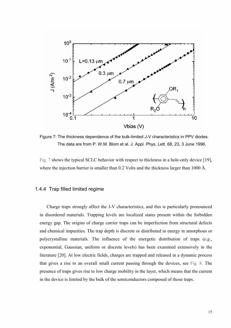
Figure 7: The thickness dependence of the bulk-limited J-V characteristics in PPV diodes.
The data are from P. W.M. Blom et al. J. Appl. Phys. Lett. 68, 23, 3 June 1996.
Fig. 7 shows the typical SCLC behavior with respect to thickness in a hole-only device [19],
where the injection barrier is smaller than 0.2 Volts and the thickness larger than 1000 Å.
1.4.4 Trap filled limited regime
Charge traps strongly affect the J-V characteristics, and this is particularly pronounced
in disordered materials. Trapping levels are localized states present within the forbidden
energy gap. The origins of charge carrier traps can be imperfection from structural defects
and chemical impurities. The trap depth is discrete or distributed in energy in amorphous or
polycrystalline materials. The influence of the energetic distribution of traps (e.g.,
exponential, Gaussian, uniform or discrete levels) has been examined extensively in the
literature [20]. At low electric fields, charges are trapped and released in a dynamic process
that gives a rise to an overall small current passing through the devices, see Fig. 8. The
presence of traps gives rise to low charge mobility in the layer, which means that the current
in the device is limited by the bulk of the semiconductors composed of those traps.

16
Figure 8: Two types of trap levels inside the polymer energy gap
When the electric field is increased, the carriers will cross the charge trap energy levels
and the traps are considered being filled. Further increment of the voltage results in injected
charge carriers cannot fall into traps, which gives rise to a dramatic increase of the current
level. This rapid transition in the J-V characteristic is defined as the trap-filled-limit (TFL)
potential. Assuming that the traps are confined in single discrete energy levels, the Mott-
Gurney equation becomes:
2
SC 0 p 3
9 VJ =8 Lγε ε µ →
2
0 p 3eff
9 VJ=8 Lγε ε µ θ t= / ( + )θ ρ ρ ρ
where Θ is the ratio between the density of free charge carrier density (ρ) and the sum of
free and trapped carrier densities (ρ+ρ t). Note that Θ=1 in the trap-free case. The
thickness is changed into an effective thickness Leff due to inhomogeneous spatial
distribution of free and trapped carriers. After most traps are filled and the TFL is reached, a
transition from trap-limited current to trap-free SCLC is observed as a rapid increase of the
current level.
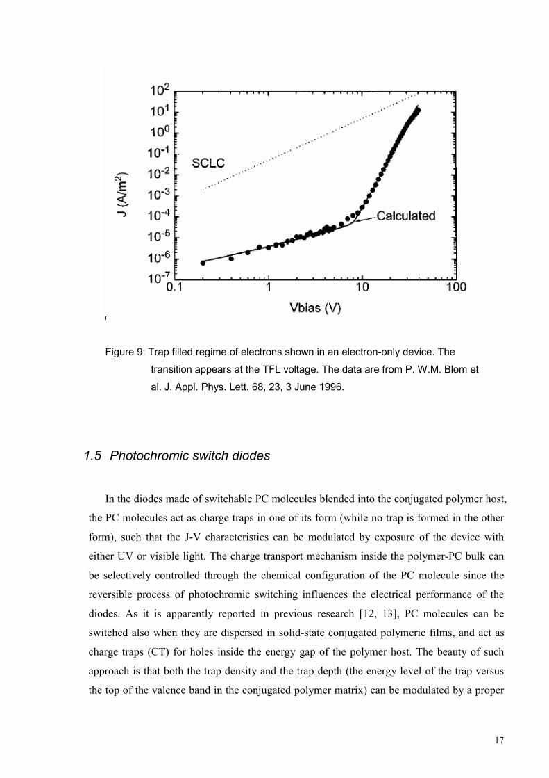
The experimental result for an electron only device with the structure Ca/PPV/Ca is
reported in Fig. 9 [19]. The J-V characteristics shows severe charge trapping and this can be
predicted by the trap model with exponentially distributed charge traps. A rapid increase of
the current appeared at the TFL voltage.
17
Figure 9: Trap filled regime of electrons shown in an electron-only device. The
transition appears at the TFL voltage. The data are from P. W.M. Blom et
al. J. Appl. Phys. Lett. 68, 23, 3 June 1996.
1.5 Photochromic switch diodes
In the diodes made of switchable PC molecules blended into the conjugated polymer host,
the PC molecules act as charge traps in one of its form (while no trap is formed in the other
form), such that the J-V characteristics can be modulated by exposure of the device with
either UV or visible light. The charge transport mechanism inside the polymer-PC bulk can
be selectively controlled through the chemical configuration of the PC molecule since the
reversible process of photochromic switching influences the electrical performance of the
diodes. As it is apparently reported in previous research [12, 13], PC molecules can be
switched also when they are dispersed in solid-state conjugated polymeric films, and act as
charge traps (CT) for holes inside the energy gap of the polymer host. The beauty of such
approach is that both the trap density and the trap depth (the energy level of the trap versus
the top of the valence band in the conjugated polymer matrix) can be modulated by a proper

18
choice of the PC-polymer pair. The device architecture together with the PC compound
utilized here can be seen in Fig. 10.
Figure 10: (a) is the cross-section of the device architecture. (b) is the photoisomerization
of PIII molecules, which corresponds to two energy states. The images are
from P. Andersson et al., Adv. Mater., 2005, 17, 1798-1803.
PIII is the acronym used for the PC molecule 1,3-dihydro-1,3,3-trimethylspiro[2H-indole-
2,3’-[3H]phenanthr[9,10-b](1,4)oxazine] (PIII, Sigma-Aldrich, 32,256-3). This PC molecule
was used as the switching material inside a MEH-PPV polymer matrix, where the latter acts
as the active diode material.
Figure 11: Energy diagram of the solid-state blend consisting of PIII and MEH-PPV. The
PIII can be switched between two energy levels when they are dispersed in
MEH-PPV, which in one of the energy levels, provide the traps for the proposed
device operation. The image is from P. Andersson et al., Adv. Mater., 2005, 17,
1798-1803.

19
The proposed device mechanism is illustrated in Fig. 11. The main idea is to create the
trap levels inside the energy gap of the MEH-PPV bulk by switching the PC molecules
blended into the polymer. PIII has a high energy gap that absorbs at short wavelengths,
typically in the ultra-violet (UV) region about 3.5 eV (denoted as state A). After UV light
irradiation, PIII switches to its low energy gap state, 1.9 eV (state B). In such way the
injected carriers start to fall down into those traps until the TFL potential is reached, which
results in a transition of the current towards SCLC. Simply summarizing, the current through
the device is adjusted via switching of PIII molecules between two states. Note that the lack
of electron injection at low voltage prevents detection of electron traps in this device.
(a) Switchable J-V characteristics
1: Pure MEH-PPV showing
SCLC
2, 4: 20% PIII blended in MEH-
PPV after exposure to visible
light
3: 20% PIII after UV light
exposure showing a transition
from charge trap limited current
behavior (CTLC) to SCLC at the
TFL potential

20
(b) Modulation of current levels and TFL potentials versus the fraction.
Figure 12a and b: (a) Modulation of J-V characteristics in blend diodes consisting of 20%
PIII molecules in MEH-PPV. (b) The fraction of PIII in blends shows the
dependence of the trap-filled-limit voltage. The data are from P.
Andersson et al., Adv. Mater., 2005, 17, 1798-1803.
Fig. 12a shows the J-V characteristics of switchable photochromic diodes based on the PIII
and MEH-PPV blend sandwiched between ITO and Al electrodes. Typically the current is
contact-limited at low forward bias, while at higher voltages the current is space-charge (SC)
or charge-trap (CT) limited. As the applied voltage approaches the activation energy of the
limiting transport mechanism, the current rapidly increases to the level of the next limiting
mechanism. Switchable traps from PC molecules modulate the electrical properties of the
PC-polymer diodes. Furthermore, in Fig. 12b, the inset shows the dependence of the trap-
filled-limit voltage versus the fraction of PIII, while the main figure shows the current
density versus the fraction of PIII. After UV exposure, all the diodes with different fraction
of PIII show roughly the same low current level, even though different voltages are applied
as shown in the inset. Thus, higher fraction of PIII corresponds to larger current modulation.
As mentioned above, the trap filled limit voltage is shifted upwards as the amount of PIII is
increasing in the blends.
Empty squares: current
densities of blend diodes before
UV light exposure
Black squares: current densities
of blend diodes after UV light
exposure
Small graph: estimated TFL
voltages

21
2 Materials and Goal
This diploma work was carried out in order to further understand switchable charge traps
in polymer diodes consisting of blends based on PC molecules and conjugated polymers, as
presented in chapter 1.4. First of all, the basic properties and switching features of the
photochromic material chosen here, PIII, are studied and reported.
2.1 Photoisomerization
PC molecules undergo chemical structural transformation, called photoisomerization,
while irradiated to specific wavelengths. Spiropyran and spirooxazine derivatives can be
switched between two states corresponding to different energy gaps shown in the absorption
spectra. In this project, the spirooxazine 1,3-dihydro-1,3,3-trimethylspiro[2H-indole-2,3’-
[3H]phenanthr[9,10-b](1,4)oxazine] (PIII, Sigma-Aldrich, 32,256-3) is chosen as the
switching material.
Spirooxazine Spiropyran
Spiropyran and spirooxazine are well-known members in the spiro-family; spiro-compounds
induce excellent coloration after irradiation to UV light and their flexible synthesis can yield
a wide variety of colors. Spirooxazine has improved fatigue resistance since a nitrogen atom
substitutes the carbon atom in the methine bridge. It attracts a lot of research interest because
fatigue resistance is an important issue for photochromic compounds. In many features
spirooxazine and spiropyran behave similarly, however the structure of their merocyanine
form leads to differences. The keto form (see Fig. 13a) is usually more stable than the
zwitterionic form (see Fig. 13b) for spirooxazine. However, in a polar surrounding,
spiropyran compounds in the merocyanine state can have a significant amount of the
zwitterionic form.

22
CH3 CH3
N
CH3
NO2
O
CH3 CH3
N+
CH3
NO2
O-
(a) Keto form (b) Zwitterionic form
Figure 13: Two isomers of spiro-compounds in the low energy gap state; the zwitterionic
form is more polar than the keto form.
The initial state of PIII has an orthogonal configuration that is colorless and referred to
the closed form. In this ground state the π-electrons do not interact with one another.
Therefore, upon UV light stimulation, heterocyclic cleavage of the spiro-carbon oxygen bond
occurs, which is allowed by a rotation of the two moieties in the molecule resulting in the
formation of a planar colored form. The colored form is a highly conjugated structure known
as the merocyanine or open form, which absorbs in the visible light region. PIII has two
forms of isomers shown in Fig. 13, and upon UV light irradiation, the PC-polymer blend is
always composed of a mix of both isomers, with a ratio depending on the dose of light
exposure.

23
Figure 14: Illustration of the bounding shapes (HOMO, LUMO) in closed and open forms of
spiropyran, which corresponds to their energy states.
The shape of the HOMO and LUMO levels in the closed and open forms as well as the
corresponding optical absorption spectra for a spiro compound are reported in Fig.14, as
calculated at the quantum-chemical level [21-23].
If PIII molecules are exposed to a wavelength coinciding with the absorption feature of
state B, they will return back to state A, as well as that PIII molecules left in the ambient
environment will switch back to A state spontaneously. Both thermal effects and
photochemistry has an impact on the conversion rate, and the photochromic reaction is
sensitive to the surroundings.
Poly(2-methoxy-5(2’-ethylhexyloxy)-1,4-phenylenevinylene) (MEH-PPV) is chosen in
this project as the host polymer matrix and, hence, the PC-polymer blend considered for the
switch diodes is PIII/MEH-PPV.

24
2.2 Goal
In general, the photochromic transition is extremely sensitive to the environment (solvent,
temperature). On the other hand, the J-V characteristics of photochromic switch diodes are
expected to depend on various device parameters (thickness of the active layer, amount of PC
molecules in the blend). In this work, we aim at understanding the effect of various factors
(solvent polarity, temperature, PC fraction, and film thickness). The polarity of the medium
can change the equilibrium between two conformations by preferential stabilization. The
temperature is another important factor, since PIII molecules can be switched thermally. In
addition, temperature also affects the relaxation of the matrices [16]. The following factors
are considered and their impacts have been investigated in this project:
(i) Solvent effect by varying the polarity
(ii) Annealing effect refers to temperature and solvent surplus inside the films
(iii) Amount of PC molecules in the PC-polymer blend affects the trap system
(iv) Thickness of the blend layer in the diodes, having influence on the J-V characteristics
3 Experimental techniques
3.1 Spincoating
Spincoating is a common process step in the semiconductor industry in order to spread
photoresist on silicon wafers. It is also an important technique in organic electronics since it
provides thin and homogeneous solid-state films. Organic molecules and polymers have the
advantage to be soluble in organic solvents. Consequently, low-cost solution processing steps
in device manufacturing is possible in organic electronics. Spincoating offers a convenient
and simple method based on rheology to obtain homogeneous films of various thicknesses.
Spincoating is done in several steps: (a) deposition of a liquid drop on the substrate, (b) slow
rotation of the substrate to spread the drop over the substrate, (c) ramp up the rotation speed
to remove the excess of viscous material, (d) spin at high speed to dry the films and obtain
homogeneous films. The schematic steps are shown in Fig. 15.

25
Figure 15: Various steps used in spin coating. Figure comes from B.D Washo, Rheology
and Modeling of the Spin Coating Process. IBM J. Res. Develop. March, 1977,
pp. 190-198.
The resulting film thickness, assuming that solvent evaporation is not too fast, can be
controlled via several parameters as illustrated in this time independent relation:
13
2 2=KCvRνδ
ω [24]
More advanced models allow describing the thickness versus time according to:
δ: dry coating thickness (after spin)
Cv: volume fraction of solids in
suspension
ν: kinematic viscosity ( μ/ρ)
ω: angular velocity
R: sample radius
K: constant

26
13
2 2=KCvRνδ
ω
11 2
2 32
41+0.395K tRων
[24]
Spincoating can provide relatively uniform films if the viscosity and the solvent’s boiling
point are appropriate. Except for the parameters mentioned above, there are other concerns
that can influence the spincoating process. First is the compatibility of the materials in term
of surface tension. Can the liquid and the substrate form a stable interface? How well does
the solution wet the surface? The wettability of the drops on the substrate should be
optimized. Secondly, the air and flow above the spinning substrate have a large impact on the
films. Third, the temperature control of the substrate can be crucial in both the spin and bake
steps.
The cons should be noticed despite the fact that spincoating owns strong pros.
The loss of material is up to 99 percent, this situation can be improved if
recycling is available
Evaporation rate can be a problem with solvents having low boiling points
Edge-bead must be removed from the top and bottom surfaces of the
substrate
Not suitable for very large substrates, because the variation in angular
velocity between the center and the edge of the substrate increases with size
3.2 Profilometer
The Profilometer (Dektak) is an instrument used to measure the surface profile of
samples, which comprises film thickness, roughness or other topographical features. Firstly,
a scratch is done in the film. And then a stylus is applied for a contact force on the sample
surface. The stylus is then laterally dragged along the surface to explore the profile of the
scratch. The vertical displacement of stylus as a function of position can deflect the change in
step height, and the vertical variation is ranged between 100 Å to 650,000 Å. The generated

27
signal from stylus movement is analyzed and displayed, and the scan speed and the scan
length control the horizontal resolution. The stylus tracking force is initially set to 5-10
milligrams. The radius of the diamond stylus is 12.5 microns.
3.3 Absorption spectroscopy
3.3.1 UV-Vis absorption spectroscopy
A spectrometer analyzing the light reflected from the surface of a solid or passing
through a liquid is functioning as the human eye; although white light composed of a broad
range of wavelengths in the ultraviolet (UV), visible and near-infrared (NIR) portions of the
spectrum can be detected. The visible light, which can be observed by human eyes, covers a
range of wavelengths from approximately 400 to 780nm. The longest visible wavelength is
red and the shortest is violet. From left to right, the colors shown in the spectrum
correspond to increasing wavelengths in Fig. 16.
Figure 16: The visible spectrum with color series of wavelengths. Image is from
http://www.cem.msu.edu/~reusch/VirtualText/Spectrpy/UV-Vis/spectrum.htm
The visible region of the spectrum includes photon energies from 36 to 72 kcal/mole, and
the near ultraviolet region, outside 200 nm, extends this energy range to 143 kcal/mole.
Generally, the electronic excitation occurs in organic molecules with the energies available
in the 200 to 800 nm spectral range. Consequently, favored electron promotion is excited
from the highest occupied molecular orbital (HOMO) to the lowest unoccupied molecular
orbital (LUMO), which results in excited states. When the molecule is exposed to light with
• Violet: 400 - 420 nm • Indigo: 420 - 440 nm • Blue: 440 - 490 nm • Green: 490 - 570 nm • Yellow: 570 - 585 nm • Orange: 585 - 620 nm • Red: 620 - 780 nm

28
an energy matching a certain electronic transition, part of the light energy will be absorbed
as the electron jumps to a higher energy orbital. The spectrometer records the wavelengths
at which absorption occurs, in combination with the strength of absorption intensity at each
wavelength. Usually the spectrum is plotted as a graph of absorbance (A) versus wavelength.
The intensity of the reference beam, which should have little or no light absorption, is
defined as I0, and the intensity of the sample beam is defined as I1. In addition, absorption
can be presented either as transmittance (T = I1/I0) or absorbance (A= log I0/I1). If no
absorption occurs, T = 1.0 and A= 0. The wavelength of maximum absorbance is a
characteristic value, defined as λmax.
The basic principle of the absorption spectroscopy is introduced from the Beer-Lambert
Law. This law defines a linear relationship between absorbance (A), concentration (M) of
absorbing molecules in the sample and the thickness of the sample crossed by the light. The
ratio between the incident light intensity and the transmitted light intensity (for a specific
wavelength) is exponentially dependent on the concentration c of absorbing molecules (at
that specific wavelength) and the thickness of the sample crossed by the light. Beer-Lambert
law is written as:
1 0- log (I /I )=A= cα
Figure 17: Illustration of Beer-Lambert Law.
Image is from http://en.wikipedia.org/wiki/Beer-Lambert_law
A is the optical absorbance
I0 is the intensity of the incident
light
I1 is the intensity after passing
through the sample
l is the sample thickness
c is the concentration of
absorbing species in the
sample
α is the absorption coefficient or
the molar absorptivity of the
absorber
λ is the wavelength of the light

29
The absorption coefficient α is wavelength-dependent and is specific to a molecule or a
material. The variation of α versus the wavelength allows drawing the absorption spectrum
of a material.
Fig. 17 shows the absorption of light passing through a sample. However, the decreased
intensity of the transmitted light can also be due to other effects such as surface reflectance
and light scattering. The Beer-Lambert Law tends to break down at very high
concentrations, especially if the sample scatters light heavily. When the light is intense,
non-linear optical processes can also cause variances. The limit of the linear relation in
Beer-Lambert Law contains:
Deviations in absorptivity coefficients at high concentrations (>0.01M) due to
electrostatic interactions between molecules in close distance
Strong scattering of light in the sample
Fluorescence or phosphorescence of the sample
Changes in refractive index at high concentration
Shifts in chemical equilibriums as a function of concentration
Stray light
3.3.2 Spectrometer operating principle
The basic components of a typical double-beam spectrometer are shown in Fig. 18.
Figure 18: Simple schematic of the operating elements in the spectrometer.
The image is from
http://www.shu.ac.uk/schools/sci/chem/tutorials/molspec/uvvisab1.htm
Each monochromatic (single wavelength) beam in turn is split into two equal intensity
beams when the source starts light generation. One beam will pass through the sample that
is studied. The other beam will travel through the reference sample; in our case, the films

30
are spun on glass substrates, and thus the transparent glass slide is used as the reference.
The intensities together with the wavelengths are then measured and recorded by the
detectors and the analyzer. For our samples, the full spectrum is taken from the ultraviolet
(UV) region, through the visible region, and to the near infrared region, 300 nm to 800 nm.
Furthermore, when the PC switching effect is recorded, the scan range is shortened to the
visible wavelengths 550nm to 660nm, since PIII molecules have colored form, which
absorbs light corresponding to the wavelengths in the same range.
As described in section 3.3.1, the absorbance is plotted versus wavelengths in the
normal spectra. Either absorbance or transmittance can be used for characterizing the
properties and electronic structures of molecules. The high accuracy of absorption
measurement allows characterizing the switching process of photochromic molecules
investigated in this project.
3.4 Electrical measurements
The electrical measurement reported in this project is focused on the I-V characteristics
of the PC-polymer diodes. A semiconductor parameter analyzer HP 4155B is used to record
the I-V curves. When the bias is applied to both electrodes of the PC-polymer diodes, the
current passing through the bulk is recorded at each voltage; in such way the I-V
characteristics can be observed and analyzed.
4 Results and Discussion
4.1 Photochromic molecules characterized by optical absorption
measurements
Before presenting the absorption spectra of thin films consisting of PIII molecules
blended in a MEH-PPV matrix, we present the information that can be extracted from pure

31
PIII films. The pure PIII film is deposited on top of the glass substrate by spin-coating (spin
speed of 1000 rpm at room temperature). The PIII molecules are dissolved in xylene at a
concentration of 7.5mg/ml solvent. The absorption spectrum of pure PIII switched between
state A and state B is shown in Fig. 19. The absorption spectra are recorded with a Perkin-
Elmer Lambda 900 UV-Vis-NIR absorption spectrometer. The spectrum of the initial A state
is taken first and another spectrum is then recorded when the molecules have been switched
to their B state upon exposure to UV light, for approximately 30 seconds by a Vilbur
Lourmat VL-208BL Hg 2×8 W light source with an intensity of 20 mW/cm2 at 365nm.
400 500 600 700
0.00
0.02
0.04
0.06
0.08
0.10
optic
al a
bsor
banc
e
wavelength (nm)
pure PIII switching PIII in B state
PIII in A state
Figure 19: The switching effect of pure PIII films in the absorption spectrum. The solid line
is the initial curve under ambient light, and the dashed-dotted line is the
spectrum after switching PIII to the B state with UV light exposure.
The solid line in Fig. 19 is the spectrum of PIII in the initial state A, which corresponds to
a high energy gap that absorbs photon energy in the UV region, i.e. at wavelengths smaller
than 400 nm, and the film looks transparent. The dash-dotted line is the spectrum of PIII in
state B taken after 30 seconds of UV light exposure. The switching effect is clearly observed
when the two spectra are compared, as well as by the human eye since the color turns from
transparent to dark blue when PIII is transformed from state A to state B. Note that the

32
absorption intensity at 600 nm of the initial state A in the spectrum indicates that there exists
a small fraction of PIII molecules in the B state before irradiation of UV light.
Fig. 20 shows the absorption spectra of MEH-PPV and PIII. The MEH-PPV peak appears at
a wavelength of roughly 500 nm, which results in an orange color. By comparing the
absorption spectra of MEH-PPV and PIII, we expect that the presence of PIII switching
intensity in a matrix of MEH-PPV will be perceptible at the wavelength about 600 nm after
exposure to UV light.
Figure 20: The spectra of pure MEH-PPV and PIII molecules in their two energy states.
The dashed line is the spectrum curve of PIII in its low energy gap (B) state
while the dotted line corresponds to the high energy gap (A) state.
Fig. 21 shows the absorption spectra of a solid-state blend where the PIII molecules are
switched between two states. The blend consists of 20 wt.-% PIII dispersed in MEH-PPV,
and both solutions have a concentration of 7.5 mg/ml chloroform. The solutions were spin-
coated with spin speed 1000 rpm at room temperature here as well. The switching effect of
PIII from state A to state B upon UV light exposure contributes, as expected from the
previous analysis, to a new absorption feature arising around 600nm. Initially, i.e. with

33
visible light exposure, the blend shows hardly any absorption intensity at this specific
wavelength, since the PIII molecules are assumed to be in their A state.
400 500 600 700
0.0
0.2
0.4
0.6
0.8
1.0op
tical
abs
orba
nce
wavelength (nm)
PIII / MEH-PPV blend switching
blend after UV exposure
initial blend
Figure 21: The switching effect in a blend consisting of PIII molecules and MEH-PPV. The
solid and dashed lines are the spectra after exposed to visible and UV light,
respectively.
4.2 Time-dependent absorption spectra of the blends
As explained in the previous section, the state of the photochromic molecules can be
probed even if the PIII molecules are blended into MEH-PPV. Based on that observation, we
investigate the time-dependence of the absorption spectra and measure how long the PIII
molecules stay in the B state (after UV exposure) in the polymer matrix. The retention time is
defined as the time needed to loose 90% of the absorbance feature at 600 nm after UV light
exposure. The retention time of PIII in blends relates to the stability of two isomers at the low
energy gap state B. Note that exposing several times alternatively to UV and visible light
could add information about fatigue. Importantly, the retention time measured in this work is
not an absolute value since it is strongly affected by the way the measurements are performed.

34
Indeed, to characterize the stability of the low energy gap isomer, visible light needs to be
irradiated onto the sample in order to detect the state. However, visible light switches back
the PIII molecules to the high energy gap isomer. Hence, to avoid artificial diminution of the
retention time estimation, the measurements are performed as follows: the wavelength range
considered is shortened to 550-660 nm for the recording of the time-dependent intensity
decay with the absorption spectrometer since this set-up results in faster scan cycles. In
addition, we have tested that PIII does not switch by the intensity provided by the light beam
from the spectrometer, thus indicating the photoisomerization is negligible when running the
optical absorption measurements. In this manner, we can compare the retention time for
various blends and samples.
Fig. 22 shows absorption scans versus time. From the previous spectra of blends, the
wavelength peak value of PIII switched to the B state locates about 600 nm. The time-
dependent switching behavior of PIII can be determined by following the absorbance at 600
nm.
580 600 620 6400.02
0.04
0.06
0.08
0.10
0.12
abso
rban
ce
wavelength (nm)
initial
after UV
60 sec. after UV
160sec. after UV
1000sec. after UV
Figure 22: The intensity of the absorbance from a blend film after switching by UV light
decays in the order of increasing time.
In Fig. 22 there is a vertical line marked at the wavelength 600 nm, where the PIII molecules
show their B state absorption peak intensity. The line most to the left is the initial absorbance

35
before UV exposure. After UV light exposure the curves are recorded versus time and are
displayed in the order of decreasing absorbance intensities. The peak values at 600 nm are
then used to obtain the graph that determines the retention time in Fig. 23.
0 100 200 300 400 5000.000.020.040.060.080.100.120.140.16
rela
tive
inte
nsity
time (second)
blends switching intensity at peak values (600nm)fitting bi-exponential decay
Figure 23: The time-dependent switching intensity of a blend film. The fitting curve is the
second order of exponential decay (see bi-exponential model following).
The curve in Fig. 23 is plotted from the absorbance values at 600 nm in the different scans
shown in Fig. 22. The five points that were chosen to plot this curve correspond to 0, 20, 60,
160 and 480 seconds after UV light exposure of the sample. The samples were stored in
darkness (without movement of the samples inside the chamber of the spectrometer) during
the measurements in order to prevent visible light exposure. Note that the intensity values are
normalized with the initial intensity before switching with UV light, which is considered to
be zero. These five points are fitted with the second order exponential decay modeling, which
strongly suggests that the switching event of PIII from state B to state A is thermally
activated, since the samples are kept in darkness during the measurement. In general, the
kinetics is multi-exponential in solid-state matrices [25]; many models have been accurately
proposed to predict the photoisomerization of spiro-compounds. The bi-exponential model is
the most common function used for photochromic transformation [26]. Here we employed
the equation of bi-exponential fitting to attract the decay rate constants.

36
[ ]0 1 1 2 2D=D exp(-k t)+ exp(-k t)α α
Where the D and D0 are the current and initial optical densities of the merocyanine form, k1
and k2 are the decay rate constants and α 1 and α 2 are the contributions of the
corresponding terms in absorption. Note that the bi-exponential model should only be
regarded as empirical rather than a mechanistic approach.
4.2.1 The solvent influence on photochromic switching
The polarity of the solvent is the first factor taken into consideration when various
solvents are compared. The influence that the polarity of the solvent has on the
photoisomerization reaction of PC molecules has been studied and reported previously [15].
In general, it is known that a polar environment can help to stabilize PC molecules in the
zwitterionic form of their low energy gap state B (see Fig. 13, section 2.1); especially for
spiropyran derivatives. Moreover, it has been suggested that most isomers of spirooxazine
in the open form exist in the keto form even in a polar solvent. Thus, a polar environment
typically stabilizes the zwitterionic form of the spirooxazine less efficiently compared to the
spiropyran.
The two solvents chosen here have different polarities: xylene has a polarity index of
2.5 and chloroform has a polarity index of 4.1, which indicates that chloroform is more
polar than xylene. Both solvents can dissolve PIII in seconds, and the solvatochromism is
apparently seen at the same time. As observed by the human eye, the color of the solution
from PIII dissolved in xylene is violet, and the color of the chloroform solution is indigo.
In dry films made of PC-polymer blends, the solvent is not expected to have a direct
influence on the isomerization reaction since their amount is likely very small. In contrast,
the solvent is expected to affect the morphology of the blend. Indeed, phase separation
between PIII domains and the MEH-PPV matrix is likely sensitive to the nature of the
solvent (polarity, boiling point). As a result, the contact area between the PIII domains and
the polymer matrix might affect the kinetics of the photoisomerization. The presence of
remaining solvent in the blends, in case of high boiling point solvent, might also influence

37
the kinetic of the isomerization reaction characterized by the retention time (see section
4.2.2).
Fig. 24a and b show the absorption spectra versus time from the blend of PIII/MEH-PPV in
xylene and chloroform. The concentration in both solutions is 7.5 mg/ml, and 20 wt.-% PIII
is mixed into the MEH-PPV polymer host. The films are spun on the glass substrates with
spin speed 1000 rpm during 20 seconds at room temperature. In Fig. 24a, the initial state
corresponds to the spectrum after visible light exposure. In that case, most of the PIII
molecules are in the high energy gap state A. However, one can observe that few PIII
molecules remain in the low energy gap state B and contribute to a weak absorbance around
600 nm. After 60 seconds of UV light exposure, the absorption spectrum is recorded and
characterized in the blend films where most of the PIII molecules now are switched to their
low energy gap state B. The kinetics of the thermally reversible isomerization is monitored
by the absorption spectrum versus time. The intensity goes down as the PIII molecules
spontaneously switch back from the B state to the A state, as shown in Fig. 24a and b.
As indicated by these results, there is hardly any difference in retention time for the
blends obtained from the two different solvents. By comparing Fig. 24a and b, the PIII
molecules switch back in about four minutes. This indicates that if there are residual solvent
molecules in the films, their nature (xylene vs. chloroform) have a negligible influence of
the kinetics of the thermally reversible isomerization.

38
560 580 600 620 640 6600.000
0.015
0.030
0.045
0.060
0.075
0.090 initial after UV 20 sec in darkness 60 sec in darkness 120 sec in darkness 220 sec in darkness
abso
rban
ce
wavelength (nm)
switching intensity v.s. time decayin blend film from xylene
(a) Absorption spectrum of a xylene-based blend films
580 600 620 640 660
0.025
0.050
0.075
0.100
0.125
abso
rban
ce
wavelength(nm)
initial after UV 20 sec in darkness 60 sec in darkness 120 sec in darkness 220 sec in darkness
switching intensity v.s.time decayin blend film from chloroform
(b) Absorption spectrum of a chloroform-based blend films

39
Figure 24: The absorption spectra of blends consisting of 20% PIII dispersed in MEH-PPV.
(a) and (b) show the switching intensity versus time recorded for two different
solvents: xylene and chloroform, respectively.
4.2.2 Annealing
Annealing treatment is an important step in solid-state device fabrication. The annealing
temperature and time of the blends formed from a xylene solution are 80℃ and 5 minutes.
For blends obtained from chloroform solution, the annealing temperature and time are 50 ℃
and 3 minutes, respectively. Xylene has much higher boiling point (135-145 ) compared ℃
to chloroform (60-65 ), which explains the more drastic annealin℃ g conditions for xylene
(increased annealing temperature and time). We annealed the samples for a certain time at a
temperature below the boiling point of the particular solvent used during the film formation.
The main purpose of the annealing treatment is to get rid of the solvent from the films after
the spincoating process. In addition, annealing has a quite obvious effect to the kinetics and
relates to many mechanisms that also could control the properties of the films. For instance,
when the sample is annealed, it gains heat energy and may affect the aggregation of
molecules, or the interface/phase of the blend might be modified.
Fig. 25b shows the time evolution of the absorbance at 600 nm for the blends formed
from the chloroform solution before annealing and after annealing. After annealing, the
retention time is 2.4 times longer. For samples based on xylene (see Fig. 25a), the annealing
treatment increases the retention time by a factor of three. The first observation is that the
annealing treatment improved the retention time of all samples. This is tentatively explained
by the presence of residual solvent molecules in the non-annealed films, which facilitates
the thermoreversible isomerization. The removal of residual solvent thus increases the
retention time. In other words, after annealing, the solvent has evaporated from the samples
and the surrounding environment of the PIII molecules is more suitable for allowing the PIII
molecules to stay in the B state.
Another interesting observation is related to the switching ratio. The switching ratio is
defined as the difference between the absorbance at 600 nm just after UV light exposure
divided by the absorbance at 600 nm after an infinite time. The switching ratio after

40
annealing decreases by 35% in films based on xylene, an effect that does not show up in
films obtained from chloroform solution. Hence, PIII in films made of xylene has more
difficulties to switch upon UV exposure. This might be explained by a higher degree of
crystallization in the PIII domains within the MEH-PPV matrix. PIII is known to crystallize
better in non-polar environments [15], which we also observed in pure PIII films obtained
from xylene (see section 5.1).
0 150 300 450 600
0.0
0.2
0.4
0.6
0.8
1.0annealing effect, blend: 20% PIII/MEH-PPVsolvent: xylene
inte
nsity
time (sec)
relatively normalized intensity, unannealed relatively normalized intensity, annealed
(a) Time-dependent intensity decay of the switching effect in blends from xylene.
The curve indicated with circles is the unannealed sample, and the curve with
triangles is the annealed sample.

41
0 150 300 450 600
0.0
0.2
0.4
0.6
0.8
1.0annealing effect, blend: 20% PIII/MEH-PPVsolvent: chloroform
inte
nsity
time (sec)
relatively normalized intensity, unannealed relatively normalized intensity, annealed
(b) Time-dependent intensity decay of the switching effect in blends from
chloroform. The curve indicated with circles is the unannealed sample,
while the curve with triangles is the annealed sample.
Figure 25: Time-dependence of the switching intensity in blend films based on either
xylene or chloroform. The fitting curve shows exponential decay of the second
order (see section 4.2).
4.2.3 Thickness dependence
Here, we establish the profile of absorbance or transmittance of the light of wavelength
600 nm through the PIII/MEH-PPV blend. The transmittance is recorded for various film
thicknesses using the same incident intensity. The Beer-Lambert law is I=I0 exp (-F×d),
where d is the thickness and F=ln 10×[PC]×α, where [PC] is the concentration of PIII
molecules in the blend and α is the molar absorption coefficient of the PC at 600 nm. Hence,
the transmission recorded for various thicknesses of the PIII-MEH-PPV blend should
follow T=I/I0=exp (-F×d).
Fig. 26 displays the exponential decay of transmittance. For the fraction of PIII used (20%)
in the blend, one can observe that 12.4 % of the light intensity is absorbed for films with a

42
thickness of 320 nm. The devices using blends will have a thickness between 18 nm and
320 nm. For this thickness range, the light can easily switch all PC molecules present in the
film.
0 50 100 150 200 250 300 3500.850.860.870.880.890.900.910.920.930.940.95
trans
mitt
ance
th ickness (nm )
thickness dep. of blends fitting Beer-Lambert Law
Figure 26: Thickness dependence of the blend films recorded as transmittance versus
various thicknesses. For the constant UV light intensity, the exponential
relationship should fit with Beer-Lambert law.
4.3 Switch diodes
After collecting data and features from absorption spectra of the PC-polymer blend films,
we used those films as active layers in an electronic device. In this section, we aim not only
at reproducing switchable diodes based on photochromic molecules, but also to further
characterize them. Two subjects of importance are to see the influence of the thickness of the
PIII/MEH-PPV blends on the I-V characteristics and to observe if switching occurs also at
low voltages, likely in the injection limited regime of the devices. In order to achieve these
goals, we would first like to understand the reproduced data from the literature related to the
MEH-PPV diodes.

43
4.3.1 Basic understanding of MEH-PPV diodes
The polymer diodes based on MEH-PPV have been introduced in chapter 1.3. In this
section, the pure MEH-PPV diodes are used as a reference available for comparison with
the blend diodes. To get four different thicknesses, four concentrations of the solutions in
chloroform are spun on ITO substrates that are pre-covered by the conducting polymer
poly(3,4-ethylenedioxythiophene)-poly(styrene sulfonate) (PEDOT:PSS, 70% Baytron P
from Bayer AG mixed with isopropanol) in order to ensure efficient hole injection from the
positive electrode. The spin speed is 1000 rpm with the time is 20 seconds and the process
is done at room temperature. To complete the device, a 2000 Å thick layer of aluminum is
deposited as the top electrode.
4 6 8 10
10
100
1000
curr
ent d
ensi
ty J
(A/m
2 )
voltage (V)
28nm 58nm 190nm 400nm
pure MEH-PPV diodes thickness dep.
Figure 27: Influence of the thickness on the current-voltage characteristics in pure MEH-
PPV diodes plotted in the high electrical field region under the assumption of
SCLC behavior.
Fig. 27 shows the thickness dependence of pure MEH-PPV diodes in I-V characteristics.
The thicknesses are measured by a DekTak Profilometer and marked at each corresponding
I-V curve. The variation in film thickness is obtained from tuning the concentration of the
solution. According to the project run previously [27], the spin time and solution
temperature have small influence, even negligible, on the thickness of MEH-PPV layer spun

44
from chloroform solution. The concentration represents 95% of the thickness dependence,
and only 5% comes from the spin-speed.
In the space charge limited current (SCLC) regime: the relation between current density
and the thickness of hole-only diodes fits Child’s law: J =c* V2/L3 as observed for MEH-
PPV diodes by Blom et. al.[19]. In an ITO/MEH-PPV/Au, hole only devices, they observed
that the interface-limited injection did not dominate the J-V characteristics even at low
voltages. In our project, the device chosen is different, since a layer of PEDOT:PSS is used
between ITO and MEH-PPV. Note also that the device considered is not a hole-only device
because aluminum is deposited as the top electrode instead of gold, and consequently
electrons are injected from the negative electrode at a certain higher voltage. This is
demonstrated by weak light coming out from the diodes that we made, which would not be
the case in a hole-only device. However, at low voltage region, there are very few electrons
injected and holes are the main charge carriers in the devices.
0.00E+000 2.00E+016 4.00E+016
0
200
400
600
800
1000
1200
cur
rent
den
sity
J (A
/m2 )
1/thickness cubed (1/Angstrom3)
pure PPV diodes thickness dep.bulk limit model in high voltages
Figure 28: Bulk-limited model fitting with pure MEH-PPV diodes in the high voltage range
(4 V). The linear relationship should follow Child’s Law: J =c* V2/L3, which
indicates that the current density is proportional to the inverse of the cubed
thickness. See reference [19].

45
In Fig. 28, the simplified linear relation of J versus 1/L3 is plotted. The values of the current
density at 4 V in each diode are plotted versus the inverse cubed thickness. The line
interpolated through the four points indicates that the MEH-PPV diodes are operating in the
SCLC regime at 4 V, which is in good agreement with the data in the literature [19].
However, at lower voltages (2 V), the relation of J versus 1/L3 is not linear anymore, which
refers to that the devices did not yet reach the SCLC regime. The current stays the same
whatever the thickness of the devices (Fig. 29), which suggests that the current passing
through the devices is charge injection-limited.
-2 0 2 4 6 8 10
1E-8
1E-7
1E-6
1E-5
1E-4
1E-3
curr
ent (
A)
voltage (V)
28nm 58nm 190nm 400nm
pure MEH-PPV diodesthickness-dep.
bulk limit
injection limit
Figure 29: I-V curves of the thickness dependence in pure MEH-PPV diodes. The vertical
line is the constant voltage for the bulk-limited model, and the horizontal line is
the constant current for the injection-limited model.
On the other hand, we have tested the model based on exponentially distributed charge traps
to our diodes, since the electrons may be trapped and the holes are not completely trap-free.
However this determination suggested by Kumar et. al.[28]did not work in our case. So
instead we model the injection-limited condition as reported by Baldo et. al.[29] in order to
see which mechanism that dominates the I-V characteristics in our devices. The voltage for

46
each thickness is plotted at a specific current level of 20µA, see the horizontal line in Fig.
30. The linear thickness dependence should demonstrate that the current is limited by the
injection of charge carriers in the devices at low voltages. This is in good agreement with
the expected behavior since the onset voltage of the diodes is constant for different film
thicknesses.
0 1000 2000 3000 40001.65
1.80
1.95
2.10
2.25
2.40
2.55
volta
ge (V
)
thickness(Angstrom)
pure PPV diodes thickness dep.injectionlimit model at low electrical field
Figure 30: Injection-limited model fitting with pure MEH-PPV diodes in the low voltage
range (current level 20 µA). The linear relationship of voltage versus thickness
is valid here.
We conclude that these diodes are injection-limited in the low electrical field region and
finally end up into the space charge-limited regime at higher applied voltages. The
transition between the two regimes is not easy to establish, but the results are in agreement
with other studies showing that MEH-PPV diodes work in the SCLC regime at higher
voltages.

47
0.00E+000 2.00E-014 4.00E-014 6.00E-014
3.0
3.5
4.0
4.5
5.0
5.5
6.0
6.5 pure PPV diodes thickness dep.bulk limit model at low electrical field
Vol
tage
squ
ared
(V2 )
thickness cubed (Angstrom3)
Figure 31: Bulk-limited model failed at low electrical field. The same current level that was
plotted in Fig. 30 is used here for the squared voltage versus the cubed
thickness.
4.3.2 The PIII/MEH-PPV switchable diodes
4.3.2.1 Typical I-V characteristics
The J-V characteristics of the PIII/MEH-PPV blend diodes have been previously
reported by Andersson P. [12, 13] and described in section 1.4. The authors showed that
switchable charge traps (CT) could control the J-V characteristics of MEH-PPV diodes
through the reversible photoisomerization of PIII molecules. Fig 12 in Chapter 1.5 displays
the J-V characteristics of PIII/MEH-PPV blend diodes as well as a sketch of the device.
The switch diodes can either let pass a low current in the trap filling regime (PIII is in the
low energy gap state) or a high current in the SCLC regime (PIII is in the high energy gap
state and does not act as a trap). Our first goal is to reproduce those results and to
investigate the influence from the thickness-dependence of the PIII/MEH-PPV blend on
the I-V characteristics. The diodes that consist of 20% PIII in MEH-PPV dissolved in

48
chloroform can be switched in a stable manner. The solutions used for the blends have
various concentrations (from 2.5 mg/ml up to 10 mg/ml), and the films are spun on ITO
glass substrates pre-covered by spin-coated PEDOT:PSS. The spin speed is 1000 rpm for
the spin time 20 seconds, and all the samples are processed at room temperature. The I-V
curves were recorded by a HP 4155B parameter analyzer, and the switching is done via 60
seconds of UV light exposure through the backside of the samples while nitrogen was
flowing on the sample surfaces in order to prevent photo-oxidation and chemical
degradation of the organic materials. The electrical performance of the devices is
measured in darkness.
-2 0 2 4 6 8
1E-8
1E-7
1E-6
1E-5
1E-4
1E-3
0.01
curr
ent (
A)
voltage (V)
initial (vis. light)
after UV
TFL
Figure 32: Typical I-V characteristics of blend diodes while PIII switches between the initial
state and the low energy gap state, which results in current modulation. The
trap-filled-limit potential appears in the high voltage range, and then the two
curves perfectly fit in the SCLC regime.
Those two curves are nice and clearly show how the trap-limited and the space charge
limited currents, SCLC are separated. The solid curve is with visible light exposure, while
the dash-dotted curve is after UV light exposure. We succeeded to reproduce similar
results as Andersson et al [12, 13]. Indeed, one can observe a clear increase of the current

49
level in the dashed curve at about 4.5 V, which corresponds to the trap-filled limit voltage
VC. At voltages lower than Vc, the current is lower than before the UV light exposure
because of the presence of traps created by the HOMO of the PIII molecules that is higher
in energy compared to the top of the valence band of MEH-PPV (see Fig. 11 in chapter
1.4). Above VC, all traps are filled and the current rises up to reach the trap-free SCLC
regime. The two curves are perfectly fitting in this region indicating the absence of traps.
Interestingly, there is another reversible phenomenon that was not observed by
Andersson et al. The onset of injection is shifted to a higher threshold voltage (1.5 V after
UV exposure instead of 1 V after visible light exposure). This feature is going to be
discussed in the forthcoming sections.
4.3.2.2 Reversibility of the switch diodes
Figs. 33a and b show three different regions in I-V characteristics of the blend diodes
(20% PIII blended into MEH-PPV dissolved in chloroform and xylene, with the
concentration 7.5mg/ml)). In Fig. 33a, the initial curve (with visible light exposure) is the
solid line very similar to the characteristics of pure MEH-PPV diodes. After UV light
exposure, the current drops down by more than one order of magnitude (dashed line, 10
times lower at 3 V). The dotted line is the characteristics of the diode after waiting a long
time in darkness (10 min). The fact that it is very similar to the initial curve indicates that
the process is unstable as was extensively discussed in the previous section. Indeed, PIII
photochromic molecules are thermoreversible and come back to their high energy gap
isomers in about 10 minutes in the blends (see section 4.2 about time evolution of the
absorption spectra). In Fig. 33b, we show an intermediate situation, where the PIII
molecules are not all back to their initial state. In reality, the dotted line is after 4 minutes
in darkness. One can observe that the I-V characteristic starts to come back to its initial
shape, which suggests that the amount of traps decreases with time. Obviously, in term of
applications, if thermoreversible PC molecules need to be used, one needs to find ways to
tune and increase the retention time.

50
-2 0 2 4 6 8 10 12 14
1E-8
1E-7
1E-6
1E-5
1E-4
1E-3
initial after UV 10min after UV
curr
ent (
A)
voltage (V)
reversibility of blend diodes switching
(a) Reversible switching of PC-polymer blend diodes from chloroform
-2 0 2 4 6 81E-8
1E-7
1E-6
1E-5
1E-4
1E-3
curr
ent (
A)
voltage (V)
uv 4min after UV initial
switching feature in blend diodes
low voltage region
TFL
SCLC
(b) Different transition regimes shown in the I-V curves of blend diodes from xylene
51
Figure 33: Typical I-V characteristics of blend diodes consisting of PIII/MEH-PPV. (a)
Shows the reversible switching effect, where the current modulation occurs
upon photoisomerization of PIII. (b) The behavior of the I-V characteristics
reflects the transition mechanism in each region. From these features the two-
trap system model is proposed in section 4.3.2.3.
In addition, this is our first observation of the interesting I-V behavior in the low
voltage region. The injection current is constrained after UV light exposure, forming a
saturation regime at a current level of about 1µA. When the threshold voltage is reached at
around 3 V, the current rises rapidly. The follow-up is also attractive: after that the device
has been kept in darkness about 10 min, the constrained saturation disappears. In contrast,
the current does not go back completely to the initial current level in the high voltage
range, which can be explained by the retention of some traps inside the bulk of blend. In
order to prove this phenomenon, we involve the thickness dependence to propose a
possible model.
4.3.2.3 Thickness dependence for PIII/MEH-PPV
In this section, we investigate the thickness-dependence of the blend diode I-V
characteristics. The blend films based on PIII/MEH-PPV are spun at a spin-speed of 1000
rpm for 20 seconds in room temperature, and the dependence of the film thickness related
to solution concentration is displayed in following data graphs.
Fig. 34 shows the I-V curves obtained for various thicknesses (18 nm, 48 nm, 150 nm,
320 nm) when the PIII molecules are in their high energy gap isomers. PIII molecules do
not act as traps and the behavior of the blend diodes under the influence of visible light is
similar to pure MEH-PPV diodes. At the onset voltages of the diodes, at about 1-1.5 V, the
current stays at a certain level whatever the thickness is of the devices, which is a good
indication to claim that the current is injection-limited in the low voltage region. As a
conclusion, there is hole-injection at about 1-1.5 V from ITO/PEDOT:PSS to MEH-PPV
for all PIII/MEH-PPV blend thicknesses considered here.

52
-2 0 2 4 6 8 10 12
1E-8
1E-7
1E-6
1E-5
1E-4
1E-3cu
rren
t (A
)
voltage (V)
18nm 48nm 150nm 320nm
injection limited
Figure 34: Thickness-dependence of the blend diodes in the initial state (with visible light
exposure). A constant current level of 20 µA is used for the injection-limited
model in the low voltage region.
Fig. 35 displays the I-V feature of the blend switch diodes after UV light exposure, i.e.
when PIII molecules are switched to the low energy gap state B. As hinted in section
4.3.2.2, there is a systematically knee in the low voltage region, together with an increase
of the slope at higher voltages. The high voltage knee corresponds to a trap-filled-limit,
TFL voltage (labeled here as Vc2) previously reported by Andersson et al [12, 13].
Although it is not easy to determine Vc2, it increases with the thickness of the blend layer.
We now focus on the phenomenon occurring at low potentials. After UV light exposure,
the current stays low and constant over a larger range of potentials. Compared with Fig. 34,
we can see that the injection onset is about 1-1.5 V initially, but after UV light exposure,
the injection current stays around 1µA until it reaches a certain threshold voltage, Vc1,
depending on the thickness (see Fig. 35). The threshold voltage Vc1 increases with the
thickness (2.05 V for d = 18 nm, 2.9 V for d = 48 nm, 4.2 V for d = 150 nm, and 5.7 V for
d = 320 nm).

53
-2 0 2 4 6 8 10 12
1E-8
1E-7
1E-6
1E-5
1E-4
1E-3
0.01
curr
ent (
A)
voltage (V)
18nm 48nm 150nm 320nm
blend diodes after UV switching
shallow traps
deep traps
Figure 35: Thickness-dependence of the blend diodes after UV light exposure, where the
PIII molecules act as charge traps inside the film bulks. The arrow line crosses
the plateau in the low electric field region, marking the deep traps, while the
second region that appears at higher voltages corresponds to shallow traps.
From the operational curves of blend diodes in their initial state, we know that holes
can be injected at 1.5 V into MEH-PPV. Hence, when the devices are exposed to UV light,
holes are also likely injected into MEH-PPV about 1- 1.5 V. However, the current stays
low and form a plateau until the threshold voltage Vc1 is reached, and then it rises rapidly.
We believe that the current in the plateau is bulk-limited and not injection-limited. In order
to further support this hypothesis, the voltage corresponding to a current of 20µA versus
the thickness of the blend films is reported in Fig. 36. The linear relationship found for the
initial state, i.e. the most stable high energy gap PIII isomeric state, indicates a charge
injection-limited regime at low voltages. In contrast, there is no nice linear relationship (at
a current level of 4.6 µA) found after exposure to UV light, which indicates that the
current is not charge injection-limited in that region. Thus, we have to explain the knee in
the I-V curves at Vc1 by a bulk transport phenomenon.

54
0 500 1000 1500 2000 2500 3000 35001.5
2.0
2.5
3.0
3.5
4.0
4.5
5.0
5.5
6.0
volta
ge (V
)
thickness(Angstrom)
initial
after UV
thickness dep. in blend diodesat low voltageinjection limited model
Figure 36: Injection-limited modeling for blend diodes in two states: the linear relationship
is kept in the initial state (with visible light exposure), while the model fails after
UV light exposure.
In order to explain the presence of two knees in the I-V characteristics shown in Fig.
35, we propose a model consisting of a two-trap system for the blends: deep traps (site 1)
and shallow traps (site 2). The holes that are injected first will fall down into the deep traps,
and then lead to the first current plateau. At the trap-filled-limit voltage Vc1, the deep traps
are filled and the current rises up dramatically. However, the holes injected into blend bulk
see the shallow traps, such that the slope of the current is still lower than the trap free
SCLC regime (as measured before UV light exposure). At the second trap-filled-limit
voltage Vc2, the current slope increases and eventually reaches the trap free space-charge-
limited current regime. The thickness dependence is observed for each region, which can
support the assumption that the interface is not too critical for the I-V characteristics, but
the bulk transport properties play an important role instead.

55
Figure 37: Illustration of the two-trap model of the blends. The sites available for charge
trapping are distributed in energy levels.
The energy levels of the two traps are located as two distinct energy distributions that
are attributed to the two isomers of the low band gap isomers: the keto form (shallow trap)
and the zwitterionic form (deep trap). While the amount of the zwitterionic form is
expected to be low in a neutral environment such as MEH-PPV matrix, the zwitterionic
form can be more stabilized in a polar environment such as at the interface with rich
PEDOT:PSS, since PSS is a very polar matrix known to be present at the surface of
PEDOT:PSS films [30].
4.3.2.4 Variation of the PIII fraction (20, 40%) in the MEH-PPV host polymer
Andersson et al. [12, 13] have shown that the switching factor (current ratio before and
after UV light exposure at the TFL potential VC) can be adjusted by the composition of the
blends. Their general conclusion regarding the influence on the PIII fraction is the
following: high fraction of PIII in the blends provides more charge traps, which in turn
switches the onset of the trap-filled-limit regime to a higher voltage (See Fig. 12 in chapter
1.5). After UV light exposure, all the diodes with different fraction of PIII show roughly
the same low current level, even though different voltages are applied. Thus higher
fraction of PIII corresponds to larger current modulation since the number of traps inside
the blends is increased.
ITO/PEDOT:PSS
MEH-PPV
1 2
h+
Site 1: deep trap Site 2: shallow trap Holes are injected from
ITO/PEDOT:PSS and then fall
into traps

56
-2 -1 0 1 2 3 4 5 6 7 8
1E-8
1E-7
1E-6
1E-5
1E-4
1E-3
curr
ent (
A)
voltage (V)
20% initial 20% UV 40% initial 40% UV
deep traps
shallow traps
fraction factor in switching
Figure 38: The PIII fraction effect on the device switching properties. The blend diodes that
contain 40% PIII dispersed in MEH-PPV has higher trap-filled-limit voltage and
steeper slope due to higher trap density and the difference in trap distribution,
respectively.
In order to check if similar trends are found for the first trap-filled limit voltage (VC1)
and the second trap-filled limit voltage (VC2), two fractions of PIII are considered: 20%
and 40% (see Fig. 38). If the low voltage transition is indeed due to a deeper trap, then we
should also be able to obtain various degrees of modulation of the current levels. By
increasing the amount of PIII from 20% to 40%, VC1 shifts towards higher voltage (from
2.5 V to 2.9 V) as expected for a trap-filled-limit voltage [13]. In the second TFL regime,
the slope of the I-V curve from 40% PIII is steeper than for the 20% PIII diode (note that
the second trap-filled-limit voltage (VC2) for the blend with 20% PIII is not easily
estimated). This trend agrees with previous work [13] and the steeper slopes in
combination with the shift of the TFL potential after UV light exposure give a hint that a
higher charge trap density exists when the PIII molecules are switched to their B state.
An important parameter that characterizes those devices is the ratio between the
current levels at the trap-filled-limit potentials Vc1 and Vc2 before and after UV light
exposure. For 20% PIII, the current ratio is 24 at Vc1 and 5.7 at Vc2. For 40% PIII, the

57
current ratio is 18 at Vc1 and 13.2 at Vc2. At Vc1, the current ratio is larger in 20% PIII
than in 40% PIII, while at Vc2, the current ratio is larger for 40% PIII.
5 First steps towards a new architecture for the switch diodes
The motivations for future works are threefold: (i) extend the retention time, (ii)
maximize the switching ratio, and (iii) design a new architecture for the switch diodes. In
order to achieve the first two goals, the PIII molecule is not the ideal candidate. As already
mentioned, PIII belongs to the class of thermoreversible photochromic compounds. They
have the property to switch back to the high energy gap state spontaneously in darkness via
thermally activated processes. Therefore, they are not appropriate for memories that require
long retention time. Instead, photoreversible molecules should be considered. This class of
photochromic molecules requires light stimulation (of a specific wavelength) in order to be
triggered, but they do not switch back at room temperature. Thus, the PIII molecule can be
used as a tool to see if new device architectures can be created.
In this section, we make the first step towards the design of a bi-layered switch diode
composed of a layer of PIII and another layer of MEH-PPV. We will first characterize the
optical properties and the retention time of the bi-layered films.
5.1 Absorption of PIII layer on top of MEH-PPV
Fig. 39 shows the optical absorption spectra of PIII in free-standing films (pure PIII in the
solutions) spincoated from xylene (left panel) and chloroform (right panel). In both graphs,
the solid lines are from their initial state, and the dashed lines are after UV light exposure,
and then the dotted lines are recorded after sample stored in darkness for 24 hours. As seen in
the figure, the differences due to the solvent are that the switching ratio is higher in xylene
films, but the retention time is longer in chloroform. Similar trends have been also observed
in blends. This is attributed to a more crystalline structure in the films obtained with xylene
[15].

58
300 400 500 600 700 800
0.00
0.02
0.04
0.06
0.08
0.10ab
sorb
ance
wavelength (nm)
Free standing filmof xylene
300 400 500 600 700 800
0.03
0.06
0.09
0.12
0.15
0.18Free standing filmof chloroform
abso
rban
ce
wavelength (nm)
Figure 39: Absorption spectra of free-standing films of PIII dissolved in two solvents. The
retention time is increased to more than 24 hours, which is larger than a factor
of 10 compared with the blend films.
However, the major difference is the retention time when films based on blends and free-
standing PIII are compared. We annealed the pure PIII films made from xylene and then
recorded the decay of the switching intensity versus time (see Fig. 40). The retention time of
free-standing PIII films is more than 24 hours, (note for easily comparing the decay versus
time, in Fig. 40 the time is plotted until 800 sec. only) as well as for films based on
chloroform, while the retention time ratio is less than a factor of 10 when compared with
blended films based on xylene.

59
0 200 400 600 8000.0
0.2
0.4
0.6
0.8
1.0no
rmal
ized
inte
nsity
time(sec)
FS unannealed in xylene Fs unannealed in chloroform FS annealed in xylene
annealing effect in free-standing films
Figure 40: Time-dependent intensity decay of the switching in free-standing PIII films with
annealing effect. The curve indicated with circles is the unannealed sample based
on chloroform, while the curve with triangles and squares are the
annealed/unannealed samples based on xylene.
If the I-V characteristics can be modulated in the diodes by switching the PIII layer, the
longer retention time observed in the free-standing PIII films compared to the blends might
also result in a longer retention time in the electrical characteristics of the switch diodes. In
other words, free-standing PIII in combination with pure MEH-PPV, in two separated layers,
could yield longer retention time, stable diode performance, and maximized current
modulation.
The free-standing film of PIII is spun on the top of the MEH-PPV film. Both PIII and
MEH-PPV are dissolved in chloroform in this case. Fig. 41 shows the optical absorption
spectra for this bi-layered film as well as those of the PIII/MEH-PPV blends studied
previously. The switching ratio is much higher in the separated layers compared to the blends.
Here we report that the retention time of the separated layers in the absorption spectra is
about 1.5 hour, which is 6 times of magnitude longer compared to the blends. Note that the

60
interface between MEH-PPV and the top PIII layer is likely not well defined, and rather
results in a blend with a gradient of the PIII fraction. This is due to that the solvent used for
the PIII solution also dissolves MEH-PPV to some extent during the spincoating step of PIII.
560 580 600 620 640 660
0.00
0.05
0.10
0.15
0.20
0.25
0.30
0.35
abso
rban
ce
wavelength (nm)
bi-layer initial bi-layer UV blend 20% initial blend 20% UV blend 40% initial blend 40% UV
bi-layers v.s. blends
Figure 41: Absorption spectra of blends and bi-layered films. The highest switching ratio is
obtained for the bi-layered film, while the lowest ratio is observed for the blend
consisting of 40% PIII. The retention time of this bi-layered film is a factor of 6.
When we record the absorption spectra from the bi-layered samples, the incident light beam
shined through the PIII layer first, and then traveled through the MEH-PPV layer, while the
MEH-PPV itself remains unaffected upon UV light exposure.
5.2 First device data
In the following we fabricate a new device based on the bi-layered active films. The bi-
layered films consisting of free-standing PIII molecules and pure MEH-PPV, both spin-
coated from chloroform solutions, are used as the active layers in the diodes. In order to

61
achieve effective injection of holes, nickel, which has a work function of 5 eV, is deposited
as the top electrode instead of aluminum. Thus, the device architecture from the bottom is
ITO/PEDOT:PSS/MEH-PPV/PIII/Ni. In this diode, holes are injected from the ITO electrode
(Ni electrode) in backward (forward) bias. The first device data is shown in Fig. 42.
-6 -4 -2 0 2 4 6
1E-8
1E-7
1E-6
1E-5
1E-4
1E-3
curr
ent (
A)
voltage (V)
bi-layer initial bi-layer UV 15min after UV
bi-layer diodes switching
Figure 42: I-V characteristics of the bi-layered device. The current modulation ratio
between the two states (initially visible light exposure and after UV light exposure,
respectively) is a factor of 1000.
The initial I-V curve (solid line in Fig. 41) corresponds to the most stable high energy
gap isomer of the PIII molecules. The current level of the hole injection from the ITO
(negative bias in Fig. 41) is higher compared to hole injection from Ni when the device is
positively biased. This is thought to be due to the lower work function of ITO, compared to
the high energy gap state of PIII serving as an injection barrier at the Ni side, which results in
a lower hole injection barrier at the ITO side. When switching the PIII layer to its low
energy gap state B (dashed line), the current level decreases 1000 times at 2 V and –2 V.
Additionally, the injection condition seems inversed. After waiting for 15 minutes, or
exposing the devices to visible light, the I-V characteristics in the dotted line is very similar
to the initial curve, which indicates that this current modulation effect is reversible and likely

62
due to reversible switch of the photochromic layer. Since the low current is observed in both
forward and backward bias, after UV light exposure, it is not defined that the current
modulation originates from control of the hole-injection. Hence, we believe that this
mechanism is possible due to bulk transport again, maybe at the interface between PIII and
MEH-PPV, or as a combination of injection control and introduction of charge traps in the
bulk. More efforts are needed in order to understand this mechanism, but the results are
promising since the current ratio in the two states of the device is one or even two orders of
magnitude larger than for the switch diodes using PIII/MEH-PPV blends.
6 Conclusions
A lot of research efforts have been invested in exploring the predictive, applicable and
general models of the switching in photochromic spiro-compounds. The factors that control
photochromic switching are all important and will continue to attract the researchers’
attention in their strive towards novel achievements in this research field.
In this project photochromic molecules are blended in a conjugated polymer matrix
(MEH-PPV). The annealing of the polymer blend appears to increase the retention time of
the low energy gap isomer of a factor 3. This is attributed to the fact that residual solvent
molecules facilitate the photoisomerization back to the high energy gap form of the
photochromic molecules. Similar observation is done in free-standing films.
Thereafter we moved on to the devices, where the I-V characteristics of the blend diodes
give valuable information and empirical data for proposing a new model. The concept of
switchable charge traps in blend diodes was reproduced according to the work reported
previously [13]. Furthermore, the retention time is consistent when the absorption features of
the blend films and the I-V characteristics of the switch diodes are compared, and this
comparison has proven to be an efficient method in order to analyze the behavior for
different materials and device concepts.
A model involving a two-trap system is proposed to explain the complex electrical
characteristics and modulation of the devices upon visible or ultraviolet light exposure. The
thickness-dependence of the electrical characteristics point out that the charge transport is
switched between injection-limited and bulk-limited upon UV light exposure in the low

63
voltage region. The diodes are operating in two different regimes upon irradiation to light of
either visible or UV wavelengths, which results in the reversible current modulation. Finally,
we designed a new device based on a bi-layered PC-polymer vertical stack serving as the
active films. The more pronounced switching effect in free-standing PIII films, together with
the stable semiconducting MEH-PPV films, provide a desired operating characteristic of the
devices. A higher switching ratio between the I-V curves in the two states has been achieved,
compared to the system based on blend films, which offers a promising possibility for future
work.

64
7 References 1. Bao, Z., Materials and fabrication needs for low-cost organic transistor circuits.
Advanced Materials, 2000. 12(3): p. 227-230.
2. Yu, G., et al., Science, 1995. 270(5243): p. 362.
3. Jakobsson, F.L.E., X. Crispin, and M. Berggren, Towards addressable organic
impedance switch devices. Applied Physics Letters, 2005. 87(6): p. 063503.
4. Ma, L., et al., Organic bistable light-emitting devices. Applied Physics Letters, 2002.
80(3): p. 362.
5. Nilsson, D., An organic electrochemical transistor for printed sensors and logic, in
Science and Technology. 2005, Linköping University: Norrköping. p. 35-45.
6. Tatezono, F., et al., Photochromic rewritable memory media: A new nondestructive
readout method. Japanese Journal of Applied Physics, Part 1: Regular Papers & Short
Notes & Review Papers, 1993. 32(9A): p. 3987-3990.
7. Tsujioka, T., et al., Japanese J. Appl. Phys., 1994. 33: p. 5788.
8. Sworakowski, J., et al. Reversible mobility switching in molecular materials controlled
by photochromic reactions. in Supramolecular Approaches to Organic Electronics and
Nanotechn., May 24-28 2004
Synthetic Metals. 2004. Strasbourg, France: Elsevier Ltd, Oxford, OX5 1GB, United
Kingdom.
9. Tsujioka, T. and K. Masuda, Electrical carrier-injection and transport characteristics
of photochromic diarylethene films. Applied Physics Letters, 2003. 83(24): p. 4978-
4980.
10. Li, J., G. Speyer, and O.F. Sankey, Conduction switching of photochromic molecules.
Physical Review Letters, 2004. 93(24): p. 248302-1.
11. Nespurek, S., P. Toman, and J. Sworakowski. Charge carrier transport on molecular
wire controlled by dipolar species: Towards light-driven molecular switch. in The 5th
International Conference on Nano-Molecular Electronics, Dec 10-12 2002
Thin Solid Films. 2003. Kobe, Japan: Elsevier.
12. Andersson, P., N.D. Robinson, and M. Berggren, Diodes based on blends of molecular
switches and conjugated polymers. Synthetic Metals, 2005. 150(3): p. 217-221.
13. Andersson, P., N.D. Robinson, and M. Berggren, Switchable charge traps in polymer
diodes. Advanced Materials, 2005. 17(14): p. 1798-1803.
14. Bouas-Laurent, H.a.H.D., Pure and Appl. Chem., 2001. 73: p. 639.

65
15. Such, G., et al., Factors Influencing Photochromism of Spiro-Compounds Within
Polymeric Matrices. Journal of Macromolecular Science - Polymer Reviews, 2003.
43(4): p. 547-579.
16. X. Crispin, P.A., N. Robinson, J. Cornil, M. and Berggren, Photochromic diodes, in
Semiconducting Polymers, G.Malliaras, Editor. 2004, Wiley: NY.
17. Davids, P.S., I.H. Campbell, and D.L. Smith, Device model for single carrier organic
diodes. Journal of Applied Physics, 1997. 82(12): p. 6319-6325.
18. Dewar, M.J.S., et al., J. Am., Chem. Soc, 1985. 107: p. 3902.
19. Blom, P.W.M., M.J.M. de Jong, and J.J.M. Vleggaar, Electron and hole transport in
poly(p-phenylene vinylene) devices. Applied Physics Letters, 1996. 68(23): p. 3308 L2
- http://dx.doi.org/10.1063/1.116583.
20. Scott, J.C., et al., Charge transport processes in organic light-emitting devices. 2nd
International Conference on Electroluminescence of Molecular Materials and Related
Phenomena (ICEL-2), May 15-May 18 1999
Synthetic Metals, 2000. 111: p. 289-293.
21. Berkovic, G., V. Krongauz, and V. Weiss, Spiropyrans and spirooxazines for
memories and switches. Chemical Reviews, 2000. 100(5): p. 1741.
22. Krongauz, V.A., In Photochromism: Molecules and Systems, in Environmental Effects
on Organic Photochromic Systems, H.D.a.H. Bous-Laurent, Editor. 1990, Elsevier
Science Publishing House: Amsterdam. p. 793.
23. Krongauz, V., Photochromic polymers. Proceedings of the 1st International
Symposium on Organic Photochromism, Sep 12-16 1993
Molecular Crystals and Liquid Crystals Science and Technology, Section A: Molecular
Crystals and Liquid Crystals, 1994. 246: p. 339-346.
24. Washo, B.D., in Rheology and Modeling of the Spin Coating Process. 1977, IBM J.
Res. Develop. p. 190-198.
25. Gardlund, Z.G., Polymer Science, Polymer Letters, 1968. 7: p. 719.
26. North, N.G.L.a.A.M., Internal rotation in molecules dispersed in polymer matrixes.
Eur. Polym, 1973. 9(4): p. 345-355.
27. Andersson, P., Statistical Process Control and Experimental Design. 2004, ITN,
University Linköping: Norrköping.
28. Kumar, V., et al., Trap density in conducting organic semiconductors determined from
temperature dependence of J-V characteristics. Journal of Applied Physics, 2003.
94(2): p. 1283-1285.

66
29. M.A.Baldo, Interface-limited injection in amorphous organic semiconductors.
PHSICAL REVIEW, 2001. 64,085201: p. 1-17.
30. Crispin, X., et al., Conductivity, morphology, interfacial chemistry, and stability of
poly(3,4-ethylene dioxythiophene)-poly(styrene sulfonate): A photoelectron
spectroscopy study. Organic Semiconductors and Devices
Journal of Polymer Science, Part B: Polymer Physics, 2003. 41(21): p. 2561-2583.

67
8 Acknowledgement In the end of this thesis, I would like to express my sincerest gratitude to the following
people who have joined my studies towards a Master of Science degree. Teachers, co-
workers, colleagues, friends, and my family, without you all, there would not have been
my name on the cover of this thesis.
Supervisor: Xavier Crispin
Je vous remercie de m’avoir offert une telle chance d’accomplir mes etudes de maître à
l ’ITN. C’est une experience plaisante d’être une membre d’Orgel, de pouvoir suivre cet
enseignement et de partager une periode de ma vie parmi vous qui restera une des plus
importantes pour moi.
Vous m’avez donné beaucoup d’instrutions profesionnelles de la façon de recherches et
d’analyse, et aussi m’avez soutenue dans chaques étapes à surmonter toutes les difficultés
que j’ai eu durant mes experiences. Je suis fière de réaliser cette thèse de maître en suivant
votre enseignement, merci.
Handler: Peter Andersson
Det har varit en ovärderlig tid att ha dig som handledare.
Jag uppskattar allting som du har gjort för mig:
Studerat papper, analyserat data, utbytt idéer, lärorika diskussioner och framför allt, allt
labbande. Du är verkligen en jättebra handledare med all din uppmärksamhet, tålamod och
vänskap. Jag värdesätter minnet av att ha arbetat med dig.
Tack så mycket Peter.
Thanks to all the people in the Organic Electronics group at ITN, and the staff at Acreo,
for such a comfortable environment and warm interflow. Tack.
All my classmates, seniors, juniors and friends, all of you enrich and color me.
My good friend, David Montag, thank you for the valuable friendship during my studies
and life spent in Sweden.
My family, sweet Mom, sisters and brother, Wen and Yu 我親愛的家人們, 大感謝.
Finally, my wise and old friend Winston Su, thanks for your encouragement, support and
suggestions through my life. You complete, complicate me. I feel like to share all my
pleasure of my studies abroad with you.