Embed Size (px)
Citation preview
WestminsterResearch http://www.westminster.ac.uk/research/westminsterresearch Compensation technique for nonlinear distortion in RF circuits for multi-standard wireless systems Kasturi Chakrabarty Faculty of Science and Technology This is an electronic version of a PhD thesis awarded by the University of Westminster. © The Author, 2014 This is an exact reproduction of the paper copy held by the University of Westminster library. The WestminsterResearch online digital archive at the University of Westminster aims to make the research output of the University available to a wider audience. Copyright and Moral Rights remain with the authors and/or copyright owners. Users are permitted to download and/or print one copy for non-commercial private study or research. Further distribution and any use of material from within this archive for profit-making enterprises or for commercial gain is strictly forbidden. Whilst further distribution of specific materials from within this archive is forbidden, you may freely distribute the URL of WestminsterResearch: (http://westminsterresearch.wmin.ac.uk/). In case of abuse or copyright appearing without permission e-mail [email protected]
COMPENSATION TECHNIQUE FOR NONLINEAR DISTORTION IN RF
CIRCUITS FOR MULTI-STANDARD WIRELESS
SYSTEMS
Kasturi Chakrabarty
A thesis submitted in partial fulfilment of the requirements of the University of Westminster
for the degree of Doctor of Philosophy
May 2014

i
ABSTRACT
Recent technological advances in the RF and wireless industry has led to
the design requirement of more sophisticated devices which can meet stringent
specifications of bandwidth, data rate and throughput. These devices are
required to be extremely sensitive and hence any external interference from
other systems can severely affect the device and the output.
This thesis introduces the existing problem in nonlinear components in a
multi-standard wireless system due to interfering signals and suggests potential
solution to the problem. Advances in RF and wireless systems with emerging
new communication standards have made reconfigurablility and tunability a very
viable option. RF transceivers are optimised for multi-standard operation, where
one band of frequency can act as an interfering signal to the other band. Due to
the presence of nonlinear circuits in the transceiver chains such as power
amplifiers, reconfigurable and tunable filters and modulators, these interfering
signals produce nonlinear distortion products which can deform the output
signal considerably. Hence it becomes necessary to block these interfering
signals using special components.
The main objective of this thesis is to analyse and experimentally verify the
nonlinear distortions in various RF circuits such as reconfigurable and tunable
filters and devise ways to minimize the overall nonlinear distortion in the
presence of other interfering signals. Reconfigurbality and tunablity in filters can
be achieved using components such as varactor diodes, PIN diodes and optical
switches. Nonlinear distortions in such components are measured using
different signals and results noted.
The compensation method developed to minimize nonlinear distortions in
RF circuits caused due to interfering signals is explored thoroughly in this
thesis. Compensation method used involves the design of novel microstrip
bandstop filters which can block the interfering signals and hence give a clean
output spectrum at the final stage. Recent years have seen the emergence of
electronic band gap technology which has “band gap” properties meaning that a
bandstop response is seen within particular range of frequency. This concept
was utilised in the design of several novel bandstop filters using defected
ii
microstrip structure. Novel tunable bandstop filters has been introduced in order
to block the unwanted signal. Fixed single-band and dual-band filters using
DMS were fabricated with excellent achieved results. These filters were further
extended to tunable structures. A dual-band tunable filter with miniaturized size
was developed and designed.
The designed filters were further used in the compensation technique where
different scenarios showing the effect of interfering signals in wireless
transceiver were described. Mathematical analysis proved the validation of the
use of a bandstop filter as an inter-stage component. Distortion improvements
of around 10dB have been experimentally verified using a power amplifier as
device under test. Further experimental verification was carried out with a
transmitter which included reconfigurable RF filters and power amplifier where
an improvement of 15dB was achieved.
iii
ACKNOWLEDGEMENTS
Firstly, I would like to express my heartfelt thanks to the director of studies,
Dr Djuradj Budimir for his continuous support and help throughout my entire
PhD work. He has not only given me valuable and sound advice but always
steered me in the right direction when things became difficult.
Secondly, I would like to express my heartiest thanks to Dr Andrzej
Tarczynski who has been a great source of inspiration throughout my academic
life in the University of Westminster and has helped me in every way possible.
I would also like to express my sincere thanks to my examiners Dr Zhirun
Hu, Dr Vassilis Kodogiannis and my chair Dr Taj Khesavarz for taking the time
to go through the entire thesis and giving me valuable comments and feedback.
My special thanks and gratitude goes to University of Westminster for the
financial support, which helped me sponsor my studies and living costs in the
United Kingdom. I am extremely grateful for their help as without that I would
not have been able to pursue and finish my studies.
I would like to sincerely thank my Gurudev, my late father, my mother and
my brother who have been responsible for helping and motivating me and
guiding me on the right path. Lastly I would like to thank the rest of my family
and friends who have been a constant source of inspiration, support system and
guidance and without whom this work would not have been possible.
KASTURI CHAKRABARTY
23, SEPTEMBER, 2013

iv
AUTHOR’S DECLARATION
I declare that all materials contained in this thesis are my own work.
v
Table of Contents
Chapter 1 Introduction
1.1 Overview of Past Research ..................................................................................... 7
1.2 Objectives of Research ........................................................................................... 9
1.3 Thesis Organization .............................................................................................. 10
1.4 References ........................................................................................................... 12
Chapter 2 Background
2.1 Microstrip Lines ..................................................................................................... 18
2.2 Nonlinear Distortion Theory .................................................................................. 23
2.3 Filter Theory.......................................................................................................... 26
2.4 References ........................................................................................................... 29
Chapter 3 Nonlinear Distortion in Passive RF Rec onfigurable
Circuits
3.1 Non linearity and Intermodulation Distortion .......................................................... 31
3.1.1 Analysis of Nonlinearity .................................................................................. 32
3.1.2 Power Series Analysis and Two Tone Test .................................................... 33
3.2 Tunable/Reconfigurable elements in RF Circuits ............................................... 36
3.2.1 PIN Diodes ................................................................................................. 36
3.2.2 Varactor Diodes .......................................................................................... 40
3.2.3 Optical Switch ............................................................................................. 43
3.2.4 Comparison between Tuning/Switching Elements ...................................... 44
3.3 Evaluation of Nonlinear Distortion in Reconfigurable Elements ......................... 45
3.4 Distortion Evaluation of RF Reconfigurable Filters ............................................. 54
3.4.1 Filters using PIN diode as Reconfigurable Element ........................................ 55
3.4.2 Filters using Optical Switch as Reconfigurable Element ................................. 65
3.5 Conclusion ............................................................................................................ 71
3.6 References ........................................................................................................... 72
vi
Chapter 4 Compact Microstrip Bandstop Filters
4.1 Microstrip Bandstop Filter Design ......................................................................... 77
4.2 Defected Microstrip Structure (DMS) .................................................................... 84
4.3 Fixed DMS Bandstop Filter Design ....................................................................... 85
4.4 Tunable DMS Bandstop Filter Design ................................................................... 98
4.4 Conclusion .......................................................................................................... 107
4.5 References ......................................................................................................... 108
Chapter 5 Compensation of Nonlinear Distortion using Novel
Bandstop Filters
5.1 Nonlinear Distortion due to Interfering Signals .................................................... 113
5.2 Compensation Techniques for Distortion Suppression ........................................ 117
5.3 Mathematical Analysis showing Interference Suppression using Novel Bandstop Filter ......................................................................................................................... 120
5.4 Experimental Verification of the Concept using Bandstop Filter .......................... 123
5.5 Conclusion .......................................................................................................... 132
5.6 References ......................................................................................................... 134
Chapter 6 Conclusion
6.1 Contributions of the Thesis ................................................................................. 139
6.2 Future Work ........................................................................................................ 140
Publications .............................................................................................................. 142
vii
List of Figures and Tables
Chapter 1
Figure 1-1: Block diagram of the super heterodyne transceiver.
Figure 1-2: Block diagram of a multi-standard system.
Figure 1-3: Block diagram of a multi-band transmitter system.
Chapter 2
Figure 2-1: Side view of microstrip transmission line showing (a) geometry (b)
electromagnetic field distribution.
Figure 2-2: Coupled line EM field distribution for (a) odd and (b) even mode.
Figure 2-3: Microstrip discontinuities and their equivalent lumped element
circuit.
Figure 2-4: Illustration of the 1dB compression point.
Figure 2-5: Illustration of the 3rd order intercept point.
Figure 2-6: Bandstop filter using admittance inverters.
Chapter 3
Figure 3-1 : Illustration of nonlinear effect showing various distortion products.
Figure 3-2: Equivalent circuits for (a) forward biased (b) reversed biased for PIN
diode.
Figure 3-3: Schematic of the PIN diode configuration.
Figure 3-4: Response showing the IMD3 for a PIN diode with Vbias =0.6V.
Figure 3-5: Variation in Pout and IMD3 with reference to different Pin when Vbias =
0.6V or ON stage.
Figure 3-6: Equivalent circuit model for varactor diode.
Figure 3-7: Schematic of the varactor model for two tone testing.
Figure 3-8: Third order intermodulation distortion produced for the varactor
diode when a reverse bias voltage of 30V is used.
Figure 3-9: Variation in Pout and IMD3 with reference to different Pin, for Vbias =
-15V.
Figure 3-10: Equivalent circuit of a silicon switch.
Figure 3-11: Photograph of the surface mounted PIN diode.
viii
Figure 3-12: Photograph of the experimental setup used for testing IMD in the
commercial PIN diode.
Figure 3-13: Spectrum showing the 3rd order intermodulation distortion for a PIN
diode for Pin =15dBm (a) with 0.5MHz (b) with 1MHz spacing.
Figure 3-14: Variation of Pout and IMD3 with respect to various input power Pin
for the PIN diode.
Figure 3-15: Variation of (a) Pout and (b) IMD with respect to various Pin for 3G
signals.
Figure 3-16: Measured 5MHz output spectrum for a 64QAM input signal for an
input power of 15dBm in a PIN diode.
Figure 3-17: Variation of (a) Pout and (b) IMD with respect to various Pin for 4G
signals.
Figure 3-18: Measured 5MHz output spectrum for a 64QAMOFDM input signal
for an input power of 15dBm in a PIN diode.
Figure 3-19: Photograph of the fabricated optical switch.
Figure 3-20: Comparison of intermodulation distortion for QPSK and 16QAM
input signal for varying input power at 2GHz for an optical switch.
Figure 3-21: Measured 5MHz output spectra for the 16QAM input signal.
Figure 3-22: Comparison of intermodulation distortion for 16QAMOFDM and
64QAMOFDM input signal for varying input power at 2GHz for an
optical switch.
Figure 3-23: Measured 5MHz output spectra for the 64QAMOFDM input signal.
Figure 3-24: Experimental set-up for distortion evaluation in reconfigurable
filters.
Figure 3-25: Photograph of the UWB reconfigurable filter (DUT).
Figure 3-26: Spectrum showing the 3rd order intermodulation distortion for a
filter with PIN diode for Pin =15dBm (a) with 0.5MHz (b) with 1MHz
spacing.
Figure 3-27: Variation of Pout and IMD3 with respect to various input power Pin
for the reconfigurable filter using PIN diode.
Figure 3-28: Graphical representation of Pout in digitally modulated signal.
Figure 3-29: Variation of (a) Pout and (b) IMD with respect to various Pin for 3G
signals using the reconfigurable filter as DUT.
Figure 3-30: Measured 5MHz output spectra for the 64QAM input signal.
ix
Figure 3-31: Variation of (a) Pout and (b) IMD with respect to various Pin for 4G
signals using the reconfigurable filter as DUT.
Figure 3-32: Measured 5MHz output spectra for the 64QAMOFDM input signal.
Figure 3-33: Photograph of the switchable filter with inserted PIN switches and
biasing resistors.
Figure 3-34: Measured 5MHz 16 QAM spectra of the filter for (a) 5V and (b) 9V
forward biasing. Measured 5MHz QPSK spectra of the filter for (c)
5V and (d) 9V forward biasing.
Figure 3-35: (a) Comparison of the distortions for a range of input power values
with three different bias voltages for QPSK input signal (b)
Comparison of the distortions for a range of input power values
with three different bias voltages for 16 QAM input signal.
Figure 3-36: Measured 5MHz (a) 16QAMOFDM (b) 64QAMOFDM spectra at
the output of the optical switch filter at 1.5GHz for Pin=10dBm in
the ON state.
Figure 3-37: Comparing the (a) output power spectrum and (b) distortion power
spectrum against the input power for 4G digitally modulated
signals.
Figure 3-38: Proposed fabricated filter with optical switch.
Figure 3-39: Measured response for (a) output power Pout (b) IMD vs Pin for
different digitally modulated signals (3G) for 2.6GHz carrier in the
ON state of the optical switch.
Figure 3-40: Measured 5-MHz (a) QPSK (b) 16 QAM and (c) 64 QAM spectra at
the output of the proposed filter at 2.6GHz carrier for 10dBm input
power in the ON state of the optical switch.
Figure 3-41: Variation of (a) Pout (b) IMD vs. Pin for different 4G digitally
modulated signals for 2.6GHz frequency in the ON state.
Figure 3-42: Measured 5-MHz spectra at the output of the optical switch filter at
2.6GHz for (a) 16QAMOFDM and (b) 64QAMOFDM for 10dBm
input power for different 4G input signals for the ON state.

x
Chapter 4
Figure 4-1: Typical bandstop filter response.
Figure 4-2: (a) Layout and (b) S-parameters of the microstrip bandstop filter.
Figure 4-3: Layout of the proposed structure of the bandstop filter.
Figure 4-4: Measured S-parameters of the designed bandstop filter.
Figure 4-5: Layout of Dual-band Bandstop Filter.
Figure 4-6: S-parameters of the dual-band bandstop filter.
Figure 4-7: Measured S-parameter response of the dual-band filter.
Figure 4-8: Simulated S21 showing tunability of the dual-band BSF.
Figure 4-9: Layout of (a) DGS and (b) DMS.
Figure 4-10: Geometry of the proposed filter using defected microstrip structure.
Figure 4-11: Current distribution of the proposed filter at 2.75GHz.
Figure 4-12: Simulated S-parameters of the proposed filter.
Figure 4-13: Simulated S-parameters of the proposed filter with varying patch
(D) dimensions.
Figure 4-14: Simulated S21 parameter of the proposed filter comparing the
effect of slabs A and B.
Figure 4-15: Photograph of the proposed bandstop filter structure.
Figure 4-16: Measured S-parameters of the proposed bandstop filter.
Figure 4-17: Comparison of measured and simulated S-parameters of the proposed bandstop filter.
Figure 4-18: Geometric configuration of the proposed filter.
Figure 4-19: Current distribution in the DMS structure.
Figure 4-20: Variation of fo with and without (w/o) stepped impedance.
Figure 4-21: Simulated S-Parameter response.
Figure 4-22: Lumped element equivalent circuit.
Figure 4-23: Flowchart of the DMS design procedure used.
Figure 4-24: Comparison of EM simulation and circuit simulation.
Figure 4-25: Photograph of the fabricated bandstop filter.
Figure 4-26: Measured response of the fabricated filter.
Figure 4-27: Geometry of the proposed dual-band DMS filter.
Figure 4-28: Current distribution of the DMS dual-band filter.
Figure 4-29: Simulated S-Parameter response of the proposed filter.

xi
Figure 4-30: Geometry of the proposed filter using varactor diode.
Figure 4-31: Photograph of the proposed tunable bandstop filter.
Figure 4-32: Measured tunable filter response for various reverse bias voltages.
Figure 4-33: Experimental set-up used to test distortion in the filter.
Figure 4-34: Measurement of distortion of proposed tunable filter using two tone
signals for Pout vs Pin and IMD vs Pin.
Figure 4-35: Spectrum showing the nonlinear distortion measurement.
Figure 4-36: Geometry of the tunable DMS filter.
Figure 4-37: Simulated S-parameters of the tunable filter for various reverse
bias voltages.
Figure 4-38: Geometry of the proposed tunable dual-band DMS filter.
Figure 4-39: Simulated S-parameters of the tunable dual-band filter for various
reverse bias voltages.
Chapter 5
Figure 5-1: Block diagram of a multi band transmitter system showing Tx1 and
IM3 suppression by a bandstop filter.
Figure 5-2: IMD products in receiver band due to transmitter.
Figure 5-3: IMD product in receiver due to CW and transmission leakage.
Figure 5-4: Block diagram of the proposed system.
Figure 5-5: Block diagram of the mixer-amplifier system without using bandstop
filter.
Figure 5-6: Simulated two-tone output spectrum of the Tx without BSF.
Figure 5-7: Simulated S-parameters of the bandstop filter.
Figure 5-8: IM3 suppression by bandstop filter.
Figure 5-9: Simulated two-tone output spectrum of the Tx with BSF.
Figure 5-10: Experimental setup for compensation technique.
Figure 5-11: Experimental S-parameters of the bandstop filter.
Figure 5-12: Measured 5MHz QPSK output spectrum of the transmitter (a)
without (b) with the bandstop filter.
Figure 5-13: Shows nonlinear distortion suppression by bandstop filter.
Figure 5-14: Simulated output spectrum comparing the responses of the power
amplifier with and without bandstop filter.
xii
Figure 5-15: Measured output spectrum of the transmitter (a) without (b) with
the bandstop filter.
Figure 5-16: Experimental set-up for Tx interference suppresion.
Figure 5-17: 5MHz QPSK output spectrum (a) without and (b) with bandstop
filter.
Chapter 1
Table 1-1: Comparison of various technologies.
Chapter 3
Table 3-1: Variation of Pout and IMD3 with reference to different Vbias when, Pin =
10dBm.
Table 3-2: Measured data for distortion evaluation using 16QAMOFDM.
Table 3-3: Measured data for distortion evaluation using 64QAMOFDM.
Chapter 4
Table 4-1: Comparison of filter size for the fixed DMS filters.
xiii
List of Acronyms
1G First-generation
2G Second-generation
3G Third-generation
4G Fourth-generation
ACPR Adjacent channel power ratio
AMPS Advanced mobile phone system
BPF Bandpass filter
BRF Band reject filter
BSF Bandstop filter
CDMA Code division multiple access
CW Continuous wave
dB Decibel
DGS Defected ground structure
DMS Defected microstrip structures
DPD Digital pre-distortion
EBG Electromagnetic band gap
EER Envelope elimination and restoration
GPS Global positioning system
GHz Gigahertz
IMD Intermodulation distortion
IMD3 Third order intermodulation product
LINC Linear amplification using nonlinear components
LO Local oscillator
LTE Long term evolution
MEMS Micro-electro-mechanical systems
MIC Microwave integrated circuit
MIMO Multiple input multiple output
mm Millimetre
MMIC Monolithic microstrip integrated circuit
OFDM Orthogonal frequency division multiplexing
xiv
PA Power amplifier
PBG Photonic band gap
PSS Photoconductive silicon switches
PSTN Public switched telephone network
QAM Quadrature amplitude modulation
QPSK Quadrature phase shift keying
RF Radio frequency
Rx Receiver
TDMA Time division multiple access
Tx Transmitter
UMTS Universal mobile telecommunication system
UWB Ultra wide band
WLAN Wireless local area network
WPAN Wireless personal area network
WMAN Wireless metropolitan area network
1
Chapter 1 Introduction
The wireless industry has seen a massive technological revolution with the
introduction of better standards providing excellent data rates, multi-standard
systems and throughput. This has led to the increasing demand for better and
more efficient subsystems which can be integrated easily and are cost effective.
New devices requiring the use of various standards in the same system has led
to an increased concern about interferences and subsequent nonlinear
distortion products in the output spectrum. Before further discussions about the
circuits which contribute to this nonlinearity, the wireless system is briefly
introduced. Wireless systems can be broadly classified as the following [1.1]-
[1.3]:
1. Cellular and fixed wireless
2. Wireless local area networks (WLANs)
3. Wireless personal area networks (WPANs)
4. Wireless metropolitan area networks (WMANs)
The history of cellular networks goes back to the introduction of the first-
generation (1G) system, followed by the more potent digital second-generation
(2G) and then the third-generation (3G) Universal Mobile Telecommunication
System (UMTS) which is based on hybrid time and code division multiple
access (TDMA/CDMA) technology. The more recent development is the 3GPP
long term evolution (LTE) system or the fourth-generation (4G) system which is
based on Multiple Input Multiple Output (MIMO) and Orthogonal Frequency
Division Multiplexing (OFDM). LTE provides a common platform for wireless
carriers and creates a commonality by covering the seventeen LTE FDD bands
and eight LTE TDD bands [1.4].
Fixed wireless networks provide connection from one fixed point such as
Public Switched Telephone Network (PSTN) to homes or business [1.5]-[1.7].
WLAN system comprises the IEEE 802.11 and HiperLAN standards. The
standards vary according to the chosen operating frequency, data rate and
range covered. WPAN systems include devices such as mobile phones,
laptops, bluetooth etc while WMAN includes WiMAX [1.2]-[1.3]. All these
systems such as HSPA, 3GPP LTE, and mobile WiMAX require radio
2
transceivers which can support high data rates and throughput. The
development of more sophisticated systems has led to a massive demand in
having glitch free, cost effective and miniaturized circuits. Hence, a primary
requirement for such advanced system is to have distortion free outputs.
Transceivers in wireless systems are a key component with which signals
are transmitted and received. In literature there are several structures of
transceivers used according to the system and specifications, but speaking
broadly, a simple transceiver consists of a baseband digital signal processing
(DSP) block, mixers, amplifiers and filters. The role of the filter is to selectively
pass or reject certain signals. The amplifier is used to bring the signal to the
appropriate power level for transmission or receiving. The baseband signals are
encoded or decoded onto a high frequency carrier. The mixers help in
converting the frequency of the signals to an appropriate level for transmission
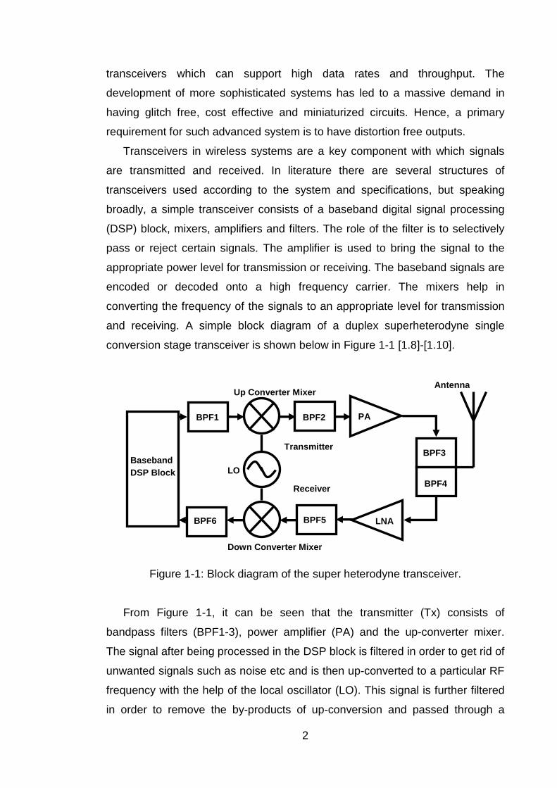
and receiving. A simple block diagram of a duplex superheterodyne single
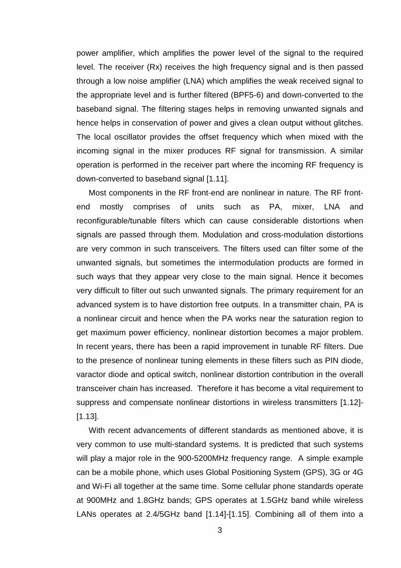
conversion stage transceiver is shown below in Figure 1-1 [1.8]-[1.10].
Figure 1-1: Block diagram of the super heterodyne transceiver.
From Figure 1-1, it can be seen that the transmitter (Tx) consists of
bandpass filters (BPF1-3), power amplifier (PA) and the up-converter mixer.
The signal after being processed in the DSP block is filtered in order to get rid of
unwanted signals such as noise etc and is then up-converted to a particular RF
frequency with the help of the local oscillator (LO). This signal is further filtered
in order to remove the by-products of up-conversion and passed through a
Baseband DSP Block
BPF1
BPF6
BPF2
BPF5
BPF3
BPF4
Up Converter Mixer
Down Converter Mixer
LO
PA
LNA
Antenna
Transmitter
Receiver
3
power amplifier, which amplifies the power level of the signal to the required
level. The receiver (Rx) receives the high frequency signal and is then passed
through a low noise amplifier (LNA) which amplifies the weak received signal to
the appropriate level and is further filtered (BPF5-6) and down-converted to the
baseband signal. The filtering stages helps in removing unwanted signals and
hence helps in conservation of power and gives a clean output without glitches.
The local oscillator provides the offset frequency which when mixed with the
incoming signal in the mixer produces RF signal for transmission. A similar
operation is performed in the receiver part where the incoming RF frequency is
down-converted to baseband signal [1.11].
Most components in the RF front-end are nonlinear in nature. The RF front-
end mostly comprises of units such as PA, mixer, LNA and
reconfigurable/tunable filters which can cause considerable distortions when
signals are passed through them. Modulation and cross-modulation distortions
are very common in such transceivers. The filters used can filter some of the
unwanted signals, but sometimes the intermodulation products are formed in
such ways that they appear very close to the main signal. Hence it becomes
very difficult to filter out such unwanted signals. The primary requirement for an
advanced system is to have distortion free outputs. In a transmitter chain, PA is
a nonlinear circuit and hence when the PA works near the saturation region to
get maximum power efficiency, nonlinear distortion becomes a major problem.
In recent years, there has been a rapid improvement in tunable RF filters. Due
to the presence of nonlinear tuning elements in these filters such as PIN diode,
varactor diode and optical switch, nonlinear distortion contribution in the overall
transceiver chain has increased. Therefore it has become a vital requirement to
suppress and compensate nonlinear distortions in wireless transmitters [1.12]-
[1.13].
With recent advancements of different standards as mentioned above, it is
very common to use multi-standard systems. It is predicted that such systems
will play a major role in the 900-5200MHz frequency range. A simple example
can be a mobile phone, which uses Global Positioning System (GPS), 3G or 4G
and Wi-Fi all together at the same time. Some cellular phone standards operate
at 900MHz and 1.8GHz bands; GPS operates at 1.5GHz band while wireless
LANs operates at 2.4/5GHz band [1.14]-[1.15]. Combining all of them into a
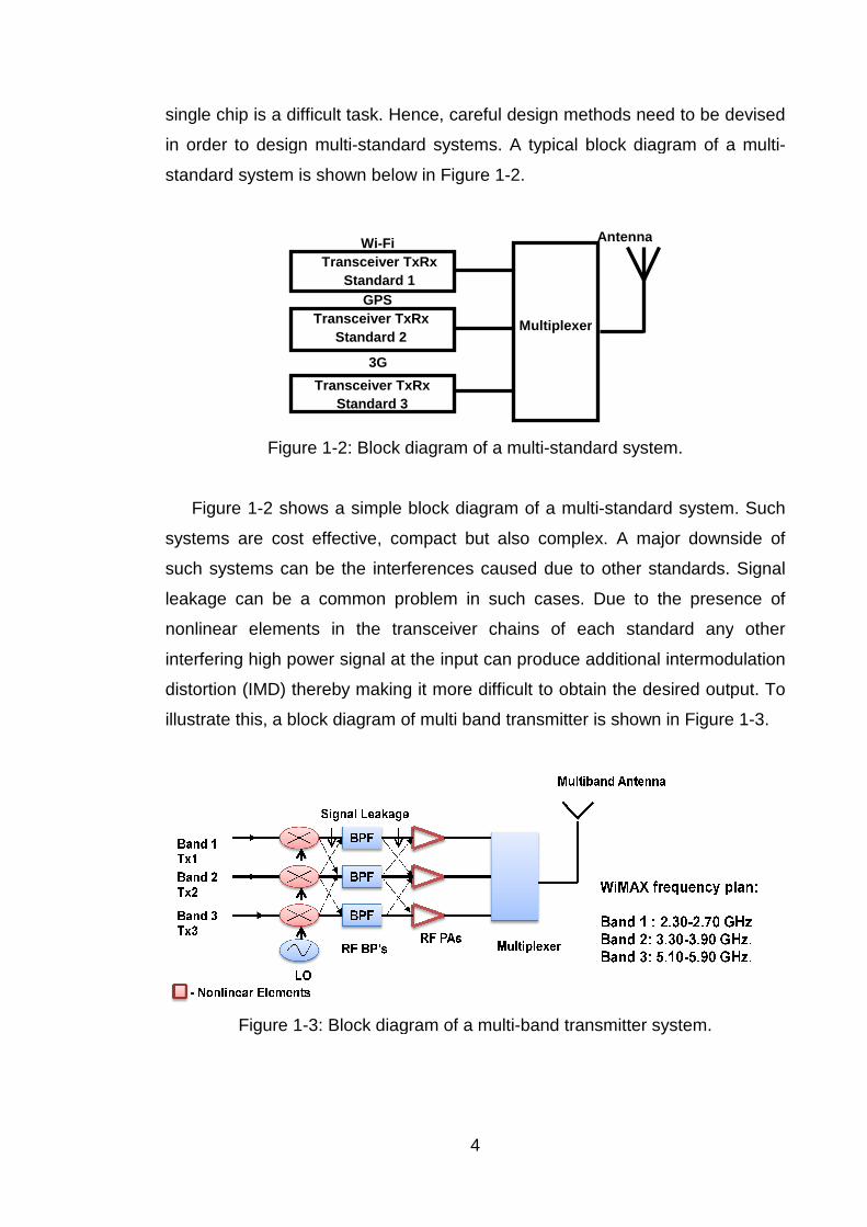
single chip is a difficult task. Hence, careful design methods need to be devised
in order to design multi
standard system is shown below in Figure 1
Figure 1
Figure 1-2 shows a simple block diagram of a multi
systems are cost effective, compact but also complex. A major downside of
such systems can b
leakage can be a common problem in such
nonlinear elements in the transceiver chains of each standard any
interfering high power signal
distortion (IMD) there
illustrate this, a block diagram of multi band transmitter
Figure 1-3: Block diagram of a multi
Transceiver TxRx
4
single chip is a difficult task. Hence, careful design methods need to be devised
in order to design multi-standard systems. A typical block diagram of a multi
tandard system is shown below in Figure 1-2.
Figure 1-2: Block diagram of a multi-standard system
ws a simple block diagram of a multi-standard system. Such
systems are cost effective, compact but also complex. A major downside of
such systems can be the interferences caused due to other standards. Signal
age can be a common problem in such cases. Due to the presence of
linear elements in the transceiver chains of each standard any
interfering high power signal at the input can produce additional
thereby making it more difficult to obtain the desired output.
block diagram of multi band transmitter is shown in Figure 1
3: Block diagram of a multi-band transmitter
Transceiver TxRx Standard 1
Transceiver TxRx Standard 2
Transceiver TxRx Standard 3
Multiplexer
AntennaWi-Fi
GPS
3G
single chip is a difficult task. Hence, careful design methods need to be devised
. A typical block diagram of a multi-
system.
tandard system. Such
systems are cost effective, compact but also complex. A major downside of
e the interferences caused due to other standards. Signal
cases. Due to the presence of
linear elements in the transceiver chains of each standard any other
additional intermodulation
making it more difficult to obtain the desired output. To
shown in Figure 1-3.
ransmitter system.
Antenna

5
Figure 1-3 illustrates the problem in the case of WiMAX signals, where Band
1 which operates at 2.5GHz, acts as an interfering signal for the transmitters in
Band 2 or Band 3. Due to the nonlinear elements in Tx2/Tx3 such as a PA, the
interfering signal causes additional nonlinear distortions making the final output
contain additional distortion components. Therefore potential solutions for such
problems need to be devised. Before a solution can be reached, it is very
important to quantify and evaluate such nonlinear distortions. This thesis partly
deals with the evaluation of nonlinear distortions in RF circuits such as
tunable/reconfigurable filters and the effect of interfering signals to the overall
measured nonlinear distortion and suggests potential compensation methods
that can be used in order to suppress such distortions. Several approaches in
minimising effects of nonlinear distortions have been studied and can be
extensively found in literature. Some of the methods of distortion suppression
can be noted as follows [1.16 – 1.19]:
1) Feed forward
2) Feedback
3) Analogue pre-distortion
4) Digital pre-distortion (DPD)
5) Injection method
This thesis however focuses on using RF filters as a method for
compensation of overall nonlinear distortion due to interfering signals [1.20]-
[1.21]. The other compensation methods have been extensively explored in
literature and each has its own drawbacks. Filters on the other band can be
simple, easily integrated and cost effective. The important question to ask here
is to what kind of filter would be a suitable option for such systems where
interferences are a major issue. In such situations, it is better to use a band
reject filter (BRF) due to the fact that such filters have low transmission loss in
the passband. This makes it a desirable property for systems where the filter is
cascaded with the rest of the structure [1.20]. The typical filter for such
application would have high attenuation properties at the interfering frequency
and low transmission loss at other frequencies.
RF and microwave filters can be designed using several technologies such
as coaxial, waveguide, and microwave integrated circuit (MIC) to name a few.
The following table summarises some of the properties of the few main
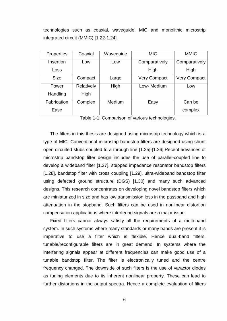
6
technologies such as coaxial, waveguide, MIC and monolithic microstrip
integrated circuit (MMIC) [1.22-1.24].
Properties Coaxial Waveguide MIC MMIC
Insertion
Loss
Low Low Comparatively
High
Comparatively
High
Size Compact Large Very Compact Very Compact
Power
Handling
Relatively
High
High Low- Medium Low
Fabrication
Ease
Complex Medium Easy Can be
complex
Table 1-1: Comparison of various technologies.
The filters in this thesis are designed using microstrip technology which is a
type of MIC. Conventional microstrip bandstop filters are designed using shunt
open circuited stubs coupled to a through line [1.25]-[1.26].Recent advances of
microstrip bandstop filter design includes the use of parallel-coupled line to
develop a wideband filter [1.27], stepped impedance resonator bandstop filters
[1.28], bandstop filter with cross coupling [1.29], ultra-wideband bandstop filter
using defected ground structure (DGS) [1.30] and many such advanced
designs. This research concentrates on developing novel bandstop filters which
are miniaturized in size and has low transmission loss in the passband and high
attenuation in the stopband. Such filters can be used in nonlinear distortion
compensation applications where interfering signals are a major issue.
Fixed filters cannot always satisfy all the requirements of a multi-band
system. In such systems where many standards or many bands are present it is
imperative to use a filter which is flexible. Hence dual-band filters,
tunable/reconfigurable filters are in great demand. In systems where the
interfering signals appear at different frequencies can make good use of a
tunable bandstop filter. The filter is electronically tuned and the centre
frequency changed. The downside of such filters is the use of varactor diodes
as tuning elements due to its inherent nonlinear property. These can lead to
further distortions in the output spectra. Hence a complete evaluation of filters
7
designed is important to check for such imperfections. This thesis explores the
design of novel tunable filters using defected microstrip structures (DMS). Such
structures can help in miniaturization due to the slow wave effect. The
application of such filters as discussed above is further explored in this thesis.
1.1 Overview of Past Research
In the 1950’s microstrip was recognised as a planar transmission line while
being further developed in the following years [1.31]. Thereafter, several planar
MICs were built using microstrip transmission lines. Several components such
as antennas [1.32], filters [1.33], power dividers [1.34], and amplifiers [1.35]
have been developed using microstrip technology. Microstrip filters are an
important part of the whole RF subsystem. A brief history into the microstrip
filter design has been provided in [1.33]. Both bandpass filters and bandstop
filters have been extensively designed in microstrip technology using advanced
design techniques such as in [1.36]-[1.40]. In [1.36], an improved hairpin filter
structure was designed using microstrip while in [1.37] a multi-stage coupled
ring bandpass filter was designed. In [1.38], a very compact dual-mode
resonator has been introduced which has effective dimensions of less than λg/4.
In [1.39] and [1.40] , a dual mode microstrip bandstop filter using inverted open
loop resonators were designed and spilt ring resonators were used in designing
a miniaturized bandstop filter respectively. Later with the introduction of
tunable/reconfigurable filters which required additional components for tuning
such as varactor diodes [1.41], PIN diodes [1.42] and optical switch [1.43] it was
imperative to study the nonlinear effects of these tuning/switching elements.
Varactor diodes having suitable properties for tuning RF circuits are
extensively used for such purposes. However due to the nonlinear characteristic
of varactor diodes, distortion measurement requires to be carried out. In
literature, distortion measurements for varactor diodes are found in several
places such as [1.44]-[1.47]. In these reviews, the varactor diodes are tested for
distortion measurements using the Volterra series. Experimental verification
using two tone signals are used in most cases. There is a lack of experimental
verification of nonlinear distortion in varactor diodes using digitally modulated
8
signals. Recently low distortion varactor diodes have been developed using
anti-parallel and anti-series varactor configuration [1.48].
In a similar fashion distortion evaluation has also been carried out for PIN
diodes and optical switches. This switching element finds application in many
RF reconfigurable filters and devices. In [1.49]-[1.52], PIN diodes have been
tested for nonlinear distortion and a third order intercept point at 40dBm is
measured approximately in [1.49]. The nonlinearity measurements in optical
switch have very little data in literature as it is a fairly new concept. Distortion
performance of an optically controlled microwave switch was proposed by
Loughborough University in [1.53].
After the evaluation of nonlinear distortion in RF filters, it is important to give
a brief history of problems faced due to interfering signals. The problems
generally occur when one signal operating in a particular band leaks and
interfere in another band very close to the original band. Due to the presence of
nonlinear components, the leaked signal combines with the main signals and
forms intermodulation distortion products which can distort the output signal
considerably. In [1.54], the effect of interfering signal is shown with numerical
analysis while [1.55] shows the effect of multi-tone interfering signal within a
communication system which leads to additional nonlinear distortions and its
effect can be seen in the output spectra.
The above problem of nonlinear distortion can be solved by various
methods. In [1.21] several methods to suppress nonlinearity due to interfering
signals are mentioned. Filters, especially bandstop filters seem to be a
favourable option as in [1.20] and [1.56]. The design of bandstop filters using
conventional approaches can be found in literature such as [1.57]-[1.58].
However DMS, a fairly new concept, having been initially proposed in [1.59]-
[1.60], exploits the “band-gap” theory. This technique draws from the previous
DGS structures but is proved to be much better in performance producing
extremely miniaturized circuits with excellent characteristics. Tunable bandstop
filters using DGS have also been proposed in [1.61]-[1.62] with excellent
results. However there is a lack of research in tunable dual-band bandstop
filters using DMS.
The literature review discusses briefly the research that has already been
done and gaps where further research needs to be carried out. There has been
9
a lack of nonlinear distortion evaluation in RF circuits using advanced digitally
modulated signals which has been addressed in this thesis. Compensation
technique using novel BSFs were also explored and experimental verification
provided. DMS filters were developed and fabricated with excellent results.
1.2 Objectives of Research
The research aims at finding a novel solution to suppress the effects of
nonlinearities due to additional interfering signals in RF circuits comprising
nonlinear elements such as PIN diode, varactor diode and optical switch.
Examples of such circuits include reconfigurable filters with optical switch and
PIN switch or a tunable filter with varactor diodes. It aims to create the solution
to the existing problem of nonlinear distortions in RF circuits demonstrating the
feasibility of the method which utilises a novel microstrip highly selective
bandstop filter in improving these distortions due to unwanted signals in various
RF circuits for multi standard wireless systems. The method aims at providing a
good compensation technique at lower cost and relatively less complexity in
design procedures. The following research objectives are undertaken:
1. Research in existing tuning/switching techniques applied to RF circuits.
Research of nonlinear distortion in nonlinear RF devices and circuits.
2. Study the analysis of nonlinear distortion in PIN diode switches, varactor
diodes and optical switches.
3. Experimental evaluation of nonlinear distortions in reconfigurable
elements such as PIN diode switches and optical switches
4. Experimentally evaluate nonlinear distortion in reconfigurable filters using
optical switch and PIN switch.
5. Study the effects of interfering signals in multi-band systems and provide
mathematical explanation to the effect of interfering signals to the overall
distortion.
6. Study methods of nonlinear distortion suppression that can be used.
7. Search for novel bandstop filter techniques that can be used in the
compensation of nonlinear distortion.
10
8. Design of novel highly selective and compact bandstop microstrip filters for
multi standard and multi band wireless applications.
9. To fabricate a novel tunable bandstop microstrip filter suitable for the
proposed technique and SDR next generation wireless multi-standard
systems
10. Investigate the nonlinear distortion compensation technique that can be
applied to bandpass filters based on PIN diode switches, optical switches
and transmitter system.
11. Experimental verification of the approach using a bandstop filter for
nonlinear distortion compensation using nonlinear RF circuit such as a
power amplifier , transmitter and reconfigurable filter as device under test
(DUT).
12. The feasibility of the proposed approach simulated with a 5-MHz digitally
modulated signal. Implement the compensation technique for nonlinear
distortion improvement of RF devices and circuits such as reconfigurable
filters and power amplifiers in transmitters.
1.3 Thesis Organization
This thesis written over a period of three years aims to provide brief
description of the motivation of the thesis, work done and contributions made. It
has been divided into several parts consisting of six chapters.
Chapter 1 provides a brief introduction to the ever changing wireless
systems. It gives an overview of systems already in use and a brief introduction
to 4G or LTE system. It explores the RF transceiver and its subcomponents
which can contribute to nonlinear distortions. This chapter also introduces the
readers to today’s modern systems such as multi-band, multi-standard systems
and the possibility of distortions due to interferences in these systems. Methods
of compensation of such distortions are suggested and the introduction of
bandstop filter as a potential method is given. The chapter details the aims and
objectives of the thesis along with an overview of past research work carried
out.
11
Chapter 2 deals with the background theory of topics covered in this thesis
along with a review of general background theory for microstrip technology. The
pros and cons are discussed. Microstrip coupled lines are introduced along with
the discontinuities of microstrip lines. A brief summary of nonlinear distortion
theory is given which details the causes of distortions, terminologies which help
in defining distortions and the major types of distortions present in wireless
transceivers. The chapter ends with a brief summary of the filter theory used.
The basic bandstop filter theory is explained along with the introduction to DGS
and DMS structures and its later use in the thesis.
Chapter 3 explains the nonlinear distortion concepts in further details with
detailed mathematical analysis. Components such as PIN diodes, varactor
diodes, optical switch etc which are used to switch or tune RF circuits are
evaluated for nonlinear distortions. The later section describes the evaluation of
nonlinear distortions in reconfigurable RF filters in further details.
Chapter 4 talks about microstrip bandstop filters that can be used to
compensate for nonlinear distortions. The chapter begins with a detailed
analysis of microstrip bandstop filter. Few filter structures using conventional
design techniques are designed and fabricated. Theory of defected microstrip
structure is introduced and several fixed single-band and dual-band novel DMS
filters are designed and fabricated. The filter structures were further designed to
be tunable for flexibility and ease of use.
Chapter 5 uses the designed bandstop filters in the compensation
techniques. A brief summary and mathematical analysis of problems in wireless
transceivers due to interfering signals are described. Compensation techniques
available in literature are briefly summarised. The mathematical proof of theory
using the bandstop filter is provided along with experimental verification using
power amplifier as device under test. Finally a transmitter Tx containing the
reconfigurable RF filter and power amplifier is tested using 5MHz QPSK signal
with and without bandstop filter showing 15dB improvement in the case with
filter as an inter-stage device.
Chapter 6 finally concludes the thesis with a brief summary of findings and
results. Contributions made to knowledge are noted and suggestions for future
work are also summarised.
12
1.4 References [1.1] D.Tse and P.Viswanath, Fundamentals of Wireless Communication,
Cambridge University Press, 2005, ISBN 0521845270.
[1.2] W. Webb, The Future of Wireless Communication, Artech House, 2001,
ISBN1580532489.
[1.3] A. Goldsmith, Wireless Communications, Cambridge University Press,
2005, ISBN 0521837162.
[1.4] D. Bondar, and D. Budimir, “Digital baseband predistortion of wideband
power amplifiers with improved memory effects,” Proc. IEEE Radio and
Wireless Symposium, Jan. 2009, pp. 284-287.
[1.5] E. Bostick, G. Bostick, The basic description of MMDS Television Systems,
Electric Press, New York, 1995, ISBN 1888552026.
[1.6] P. M. Shankar, Introduction to Wireless Systems, John Wiley & Sons, Inc.,
2002, ISBN 0471321672.
[1.7] W. E. Evans, K. G. Balb, “Application Consideration for Low-Power
MMDS”, Private cable magazine (USA) and Cable communications (Canada),
October 1991.
[1.8] F. Ellinger, Radio Frequency Integrated Circuits and Technologies, Berlin:
Springer, 2007.
[1.9] Q. Gu, RF System Design of Transceivers for Wireless Communications.
New-York: Springer, 2005.
[1.10] M. N. S. Swamy and K.-L. Du, Wireless Communication Systems: From
RF Subsystems to 4G Enabling Technologies, New York: Cambridge University
Press, 2010.
[1.11] A. Hussain, Advance RF Engineering for Wireless Systems and
Networks, John Wiley, New Jersey, 2005, ISBN 0471674214.
[1.12] D. Bondar, and D. Budimir, “Digital baseband predistortion of wideband
power amplifiers with improved memory effects,” in Proc. IEEE Radio and
Wireless Symposium, Jan. 2009, pp. 284-287.
[1.13] K. M. Gharaibeh, Nonlinear Distortion in Wireless Systems: Modeling and
Simulation with MATLAB, Wiley, 2011.
[1.14] S. Wu and B. Razavi “A 900-MHz/1.8-GHz CMOS Receiver for Dual-
band Applications” IEEE Journal of Solid State Vol-33, No-12, December 1998.

13
[1.15] M. Zargari et. al “A single-chip Dual-band Tri-Mode CMOS Transceiver
for IEEE 802.11a/b/g Wireless LAN IEEE Journal of Solid State Vol-39, No-12,
December 2004.
[1.16] S. P. Stapleton, “Adaptive feed forward linearization for RF power
amplifiers,” in Proc. 55th Automatic RF Techniques Group Conference Digest-
Spring, vol. 37, pp. 1-7, June 2000.
[1.17] Y. Y. Woo, J. Kim, J. Yi, S. Hong, I. Kim, J. Moon, and B. Kim, “Adaptive
digital feedback predistortion technique for linearizing power amplifiers,” IEEE
Trans. Microw. Theory Tech., vol. 55, no. 5, pp. 932-940, May 2007.
[1.18] S. P. Stapleton and F. C. Costescu, “An adaptive predistorter for a power
amplifier based on adjacent channel emission,” IEEE Trans. Microw. Theory
Tech., vol. 41, no. 1, pp. 49–56, Feb. 1992.
[1.19] N. Mizusawa, and S. Kusunoki, “Third- and fifth-order baseband
component injection for linearization of the power amplifier in a cellular phone,”
IEEE Trans. Microw. Theory Tech., vol. 53, no. 4, pp. 3327-3334, Apr. 2005.
[1.20]H.Uchida,H.Kamino,K.Totani,N.YonedaM.Miyazaki,Y.Konishi,S.Makino,J.
Hirokawa and M. Ando, ”Dual-Band-Rejection Filter for Distortion Reduction in
RF Transmitters”, Microwave Symposium Digest (MTT),vol.52,no.11,pp.2550-
2556, 2004.
[1.21] E.C. Niehenke, “Linearization Techniques for Advanced Transmitter
Architectures,” IEEE IMS2003, Workshop, WSB-3, 2003.
[1.22] R. J. Cameron, C. M. Kudsia, and R. R. Mansour, Microwave filters for
communication systems: fundamentals, design, and applications. Hoboken,
New Jersey: John Wiley & Sons, 2007.
[1.23] J. G. Hong and M. J. Lancaster, Microstrip Filters for RF/Microwave
Applications, New York: John Wiley & Sons, 2001.
[1.24] I. C. Hunter, Theory and design of microwave filters. London: Institution of
Electrical Engineers, 2001.
[1.25] G. Matthaei, L. Young, and E.M.T Jones, Microwave impedance-
matching networks, and coupling structures, Artech House, Boston, MA, 1980
[1.26] I. C. Hunter, J.D. Rhodes, "Electronically Tunable Microwave Bandstop
Filters," Microwave Theory and Techniques, IEEE Transactions on, vol.30, no.9,
pp.1361-1367, Sep. 1982.
14
[1.27] M.K. Mandal, K. Divyabramham, and S. Sanyal, “Sharp-rejection
wideband bandstop filters”, IEEE Microw. Wirel. Compon. Lett., vol.18, no.10,
pp. 662-664, 2008.
[1.28] V.K. Velidi, A.B. Guntupalli, and S. Sanyal, “Sharp-rejection ultrawide
bandstop filters”, IEEE Microw. Wirel. Compon. Lett., vol.19, no.8, pp. 503–505,
2009.
[1.29] H. Shaman, and J.S.Hong, “Wideband bandstop filter with cross coup-
ling”, IEEE Trans. Microw. Theory Tech., vol. 55, no.8, pp. 1780–1785m, 2007.
[1.30] F. Chen; N. Zhang; P. Zhang; Q. Chu, "Design of ultra-wideband
bandstop filter using defected ground structure," Electronics Letters, vol.49,
no.16, pp.1010- 1011, Aug. 1 2013.
[1.31] H. Howe “Microwave Integrated Circuits--An Historical Perspective,"
Microwave Theory and Techniques, IEEE Transactions on, vol.32, no.9,
pp.991- 996, Sep 1984.
[1.32] C. Peixeiro, "Microstrip patch antennas: An historical perspective of the
development," Microwave & Optoelectronics Conference (IMOC), 2011
SBMO/IEEE MTT-S International, vol., no., pp.684-688, Oct. 29 2011-Nov. 1
2011.
[1.33] R. Levy, B. Cohn, "A History of Microwave Filter Research, Design, and
Development," Microwave Theory and Techniques, IEEE Transactions on,
vol.32, no.9, pp.1055-1067, Sep 1984.
[1.34] A.M. Moselhy, A.M. Nassar, M.A. El Gazzar, "Analysis and design of
microstrip power divider," Signals, Systems, and Electronics, 1995. ISSSE '95,
Proceedings., 1995 URSI International Symposium on, vol., no., pp.545-548,
25-27 Oct 1995.
[1.35] T.Horng; S. Wu, "Radiation from a microstrip amplifier," Microwave
Theory and Techniques, IEEE Transactions on, vol.50, no.8, pp.2005-2010,
Aug 2002.
[1.36] A. Lotfi-Neyestanak, A. Lalbakhsh, "Improved microstrip hairpin-line
bandpass filters for spurious response suppression," Electronics Letters, vol.48,
no.14, pp.858-859, July 5 2012.
[1.37] A. Griol, J. Marti, L. Sempere, "Microstrip multistage coupled ring
bandpass filters using spur-line filters for harmonic suppression," Electronics
Letters, vol.37, no.9, pp.572-573, 26 Apr 2001.
15
[1.38] J.S. Hong, H. Shaman and Y.H. Chun, “Dual-mode microstrip open-loop
resonators and filters”, IEEE Transactions on Microwave Theory and
Techniques, vol. 55, no. 8, pp. 1764-1770, Aug. 2007.
[1.39] G.M. Eryilmaz, G.B. Elif, G.C. Adnan and K.D. Ceyhun, "Dual-mode
microstrip bandstop filters," Microwave Conference, 2008. APMC 2008. Asia-
Pacific, vol., no., pp.1-4, 16-20 Dec. 2008.
[1.40] J. Lee, Y. Oh and N. Myung, "A novel compact microstrip bandstop filter
based on complementary split-ring resonators," Microwave Conference, 2006.
APMC 2006. Asia-Pacific, vol., no., pp.1435-1438, 12-15 Dec. 2006.
[1.41] B. Kim, S. Yun, “Varactor-tuned combline bandpass filter using step-
impedance microstrip lines”, IEEE Transactions on Microwave Theory and
Techniques, vol. 52, no. 4, pp.1279-1283, Apr. 2004.
[1.42] M.F. Karim, X. Yong, Z.N.; Chen and L.C. Ong, "Miniaturized
reconfigurable filter using PIN diode for UWB applications," Microwave
Symposium Digest, 2008 IEEE MTT-S International , vol., no., pp.1031-1034,
15-20 June 2008.
[1.43] L. Athukorala, K. Rabbi, C. Panagamuwa, J.C. Vardaxoglou, M.
Philippakis and D. Budimir, "Optically reconfigurable microstrip UWB bandpass
filters," Antennas and Propagation Conference (LAPC), 2010 Loughborough ,
vol., no., pp.617- 620, 8-9 Nov. 2010.
[1.44] J.H. Mulligan and A. Paludi, "Varactor Tuning Diodes as a Source of
Intermodulation in RF Amplifiers," Electromagnetic Compatibility, IEEE
Transactions on, vol.EMC-25, no.4, pp.412-421, Nov. 1983.
[1.45] M.F.A. Khalid, A.S. Holland, J.R. Scott and K. Ghorbani, "Analysis of
third-order intermodulation distortion in BST varactors," Microwave Conference
Proceedings (APMC), 2010 Asia-Pacific, vol., no., pp.650-653, 7-10 Dec. 2010.
[1.46] L. Dussopt and G.M. Rebeiz, "Intermodulation distortion and power
handling in RF MEMS switches, varactors, and tunable filters," Microwave
Theory and Techniques, IEEE Transactions on, vol.51, no.4, pp.1247-1256, Apr
2003.
[1.47] B.E. Carey-Smith and P.A. Warr, "Distortion Mechanisms in Varactor
Diode-Tuned Microwave Filters," Microwave Theory and Techniques, IEEE
Transactions on, vol.54, no.9, pp.3492-3500, Sept. 2006.
16
[1.48] K. Buisman, L.C.N. de Vreede, L.E.Larson, M. Spirito, A. Akhnoukh,
T.L.M. Scholtes and L.K. Nanver, "Distortion-free varactor diode topologies for
RF adaptivity," Microwave Symposium Digest, 2005 IEEE MTT-S International ,
12-17 June 2005.
[1.49] R.H. Caverley and G. Hiller, "Distortion properties of MESFET and PIN
diode microwave switches," Microwave Symposium Digest, 1992., IEEE MTT-S
International , vol., no., pp.533-536 vol.2, 1-5 June 1992.
[1.50] R.H. Caverly and G. Hiller, "Distortion in microwave and RF switches by
reverse biased PIN diodes," Microwave Symposium Digest, 1989., IEEE MTT-S
International , vol., no., pp.1073,1076 vol.3, 13-15 June 1989.
[1.51] R.H. Caverly, "Distortion modeling of PIN diode switches and
attenuators," Microwave Symposium Digest, 2004 IEEE MTT-S International ,
vol.2, no., pp.957-962 Vol.2, 6-11 June 2004.
[1.52] R.H. Caverly and G. Phaneuf, "Nonlinear and transient microwave and
RF modeling of the PIN diode," Circuits and Systems, 1989, IEEE International
Symposium on, vol., no., pp.2209-2214 vol.3, 8-11 May 1989.
[1.53] E.K. Kowalczuk, R.D. Seager, C.J. Panagamuwa, K. Bass and J.C.
Vardaxoglou, "Optimising the performance of an optically controlled microwave
switch," Antennas and Propagation Conference (LAPC), 2012 Loughborough ,
vol., no., pp.1-5, 12-13 Nov. 2012.
[1.54] R. W.Ottinger, “The Effect of Hard Limiting in the Presence of Large Out-
of-Band Interfering Signals," Aerospace and Electronic Systems, IEEE
Transactions on, vol.AES-3, no.5, pp.830-834, Sept. 1967.
[1.55] L.B. Milstein, S. Davidovici, D.L. Schilling, "The Effect of Multiple-Tone
Interfering Signals on a Direct Sequence Spread Spectrum Communication
System," Communications, IEEE Transactions on, vol.30, no.3, pp.436-446,
Mar 1982.
[1.56] T. Ito, M. Kanemaru, S. Furuya, D. Huy , K. Okada and A. Matsuzawa,
"A 0.8–1.5GHz multi-standard WCDMA receiver with an inter-stage tunable
notch filter," Microwave Conference (EuMC), 2010 European , pp.1118-1121,
28-30 Sept. 2010.
[1.57] K.S.Chin, J.H. Yeh, and S.H. Chao, “Compact dual-band bandstop filters
using stepped-impedance resonators", IEEE Microw. Wireless Compon.Lett.,
vol.17, no. 12, pp. 849–851, 2007.
17
[1.58] V.K.Velidi and S.Sanyal, “Compact planar dual-wideband bandstop filters
with cross coupling and open-ended stepped impedance resonators”, ETRI
Journal, vol.32, no.1, 2010.
[1.59]J. Lim, Skim, Yulee, D. An and S. Nam, "Design of lowpass filters using
defected ground structure and compensated microstrip line," Electronics
Letters, vol.38, no.22, pp.1357-1358, 24 Oct 2002.
[1.60] J.A. Tirado-Mendez, H. Jardon-Aguilar, "Comparison of defected ground
structure (DGS) and defected microstrip structure (DGS) behaviour at high
frequencies," Electrical and Electronics Engineering, (ICEEE). 1st International
Conference on, vol., no., pp.7-10, 8-10 Sept. 2004.
[1.61] D.Woo, T.Lee, J.Lee, C.Pyo and W.Choi, "Novel U-slot and V-slot DGSs
for bandstop filter with improved Q factor," Microwave Theory and Techniques,
IEEE Transactions on, vol.54, no.6, pp.2840-2847, June 2006.
[1.62] S.Huang and Y.Lee, "A Compact E-Shaped Patterned Ground Structure
and Its Applications to Tunable Bandstop Resonator," Microwave Theory and
Techniques, IEEE Transactions on, vol.57, no.3, pp.657-666, March 2009.
18
Chapter 2 Background
This chapter gives a concise summary of the background theory of the
various topics covered in this thesis. The main consideration of the thesis was
to evaluate and compensate for nonlinear distortions in RF circuits for a multi-
standard wireless system using DMS bandstop filters. In most systems the
occurrence of interfering signals is a common issue. The problem arises when
the interfering signals combine with the other main signals and are passed
through nonlinear elements giving rise to intermodulation distortion components
which affects the final output to a great deal. Nonlinear components in a
wireless transceiver could be a power amplifier, a low noise amplifier, a mixer or
a reconfigurable/ tunable RF filter. In this thesis RF filters having nonlinear
tuning/switching elements such as varactor diode, PIN diode and optical switch
are extensively studied for distortions. A novel bandstop filter using defected
microstrip structure is developed in order to get rid of the problem of interfering
signals and hence reducing the overall distortions.
Hence it is important to delve into the background theory of microstrip
technology which was used to design these RF circuits, the theory of
nonlinearity and finally a glimpse into the bandstop filter theory. These three
major elements form the core of the thesis and therefore briefly described here.
The discussion starts with the overview of microstrip lines and is discussed in
detail in the next section.
2.1 Microstrip Lines
Transmission lines being the medium of propagation between two places for
em waves or other form of energy does so with minimum signal loss and
interference and are commonly used in many applications [2.1]. In literature,
there is a variety of choice in transmission line which includes microstrip,
stripline and finline to name a few. Among these entire collections, microstrip
transmission line has proved to be very popular in the design of filters and other
applications.

19
These can provide a good frequency range up to 110GHz, beyond which the
quasi-TEM approximation of the microstrip line is not valid which results in the
waves travelling at different speeds increasing the dispersion effect
considerably at higher frequencies. The losses in the microstrip line also
increases with higher frequencies which renders it unsuitable [2.2]. The
unloaded quality factor of such lines are around 250 at 30GHz, while the
characteristic impedance ranges from 20-125 Ω and the ease of fabrication
using printed circuit board (PCB) technology are some of the desirable qualities
of this planar transmission line [2.2]-[2.3].
The structure of the microstrip line contains a dielectric substrate which is
present between a thin strip of metal conductor at the top and a ground plane at
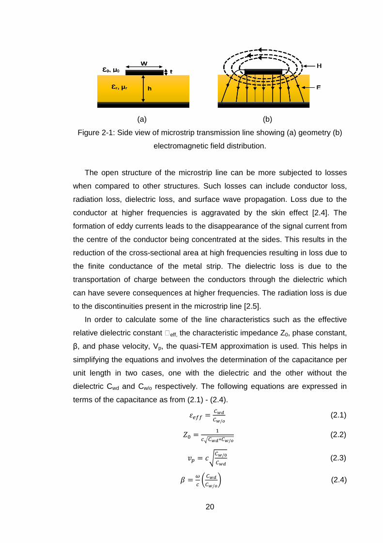
the bottom. Figure 2-1 shows the side view of the microstrip line along with the
field distribution. The thin metallic conductor has a width of W and a thickness
of t which is negligible. The dielectric layer has a height of h and a dielectric
constant of Ԑr and relative permeability of µr. The air dielectric constant is given
as Ԑ0 and the permeability as µ0.
Inhomogeneous nature of microstrip line is due to the presence of two
dielectric media (substrate and air), the electromagnetic field in the microstrip
line, meaning it has its presence in both air and the dielectric as shown from the
field distribution in Figure 2-1 (b). The electric field E is concentrated in the
dielectric medium itself while the magnetic field H extends in both medium. Due
to this inhomogeneous nature a pure transverse electric and magnetic (TEM)
wave cannot be supported. This is due to the varying speeds of propagation of
the waves in two different mediums namely air and dielectric. When the
horizontal components of the field are greater than the longitudinal components,
the quasi-TEM approximation is used while solving the characteristics of the line
[2.2]-[2.5].
20
(a) (b)
Figure 2-1: Side view of microstrip transmission line showing (a) geometry (b)
electromagnetic field distribution.
The open structure of the microstrip line can be more subjected to losses
when compared to other structures. Such losses can include conductor loss,
radiation loss, dielectric loss, and surface wave propagation. Loss due to the
conductor at higher frequencies is aggravated by the skin effect [2.4]. The
formation of eddy currents leads to the disappearance of the signal current from
the centre of the conductor being concentrated at the sides. This results in the
reduction of the cross-sectional area at high frequencies resulting in loss due to
the finite conductance of the metal strip. The dielectric loss is due to the
transportation of charge between the conductors through the dielectric which
can have severe consequences at higher frequencies. The radiation loss is due
to the discontinuities present in the microstrip line [2.5].
In order to calculate some of the line characteristics such as the effective
relative dielectric constant Ԑeff, the characteristic impedance Z0, phase constant,
β, and phase velocity, Vp, the quasi-TEM approximation is used. This helps in
simplifying the equations and involves the determination of the capacitance per
unit length in two cases, one with the dielectric and the other without the
dielectric Cwd and Cw/o respectively. The following equations are expressed in
terms of the capacitance as from (2.1) - (2.4).
/ (2.1)
/ (2.2)
/ (2.3)
/ (2.4)
21
Where, c is the speed of light in free space and ω is the angular frequency.
Recent computation techniques use Maxwell’s equation to be solved using
advanced numerical methods enabling more accurate values for the
transmission line characteristics. Software packages such as Agilent ADS use a
full wave electromagnetic analysis to solve the same characteristics more
accurately [2.6].
Another important concept is that of a microstrip coupled line. This has a
wide range of application including filter design, couplers etc. Due to the
presence of two transmission lines close to each other, coupling occur which
results in the interaction of the electromagnetic field as shown in Figure 2-2.
There are two modes of propagation supported by the coupled lines which are
the even and the odd mode as shown.
(a) (b)
Figure 2-2: Coupled line EM field distribution for (a) odd and (b) even mode.
The odd mode is created when the two transmission lines have opposite
voltage which gives rise to an electric wall. The even mode is caused due to
equivalent potential for the coupled transmission lines. This in turn gives rise to
a symmetric magnetic wall. The distribution of the EM field is irregular in nature
and this property gives rise to different phase velocities, effective dielectric
constant and other characteristics of the line .In order to analyze such cases,
characteristics due to both even and odd mode needs to be considered. When
designing coupled resonators, it becomes imperative to set the coupling
strength. Even though the coupling is a contribution of both fields, the structure
can be designed in such a way so as to create a destructive coupling or a
constructive coupling depending on the need [2.7]-[2.8].
22
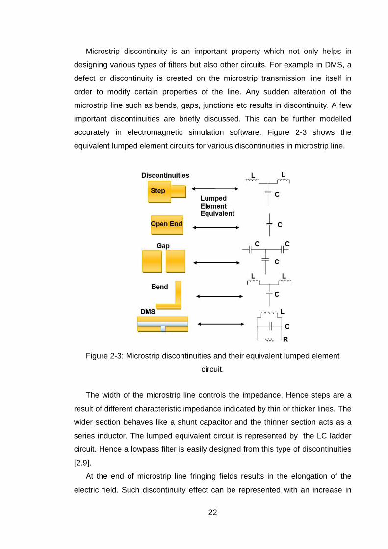
Microstrip discontinuity is an important property which not only helps in
designing various types of filters but also other circuits. For example in DMS, a
defect or discontinuity is created on the microstrip transmission line itself in
order to modify certain properties of the line. Any sudden alteration of the
microstrip line such as bends, gaps, junctions etc results in discontinuity. A few
important discontinuities are briefly discussed. This can be further modelled
accurately in electromagnetic simulation software. Figure 2-3 shows the
equivalent lumped element circuits for various discontinuities in microstrip line.
Figure 2-3: Microstrip discontinuities and their equivalent lumped element
circuit.
The width of the microstrip line controls the impedance. Hence steps are a
result of different characteristic impedance indicated by thin or thicker lines. The
wider section behaves like a shunt capacitor and the thinner section acts as a
series inductor. The lumped equivalent circuit is represented by the LC ladder
circuit. Hence a lowpass filter is easily designed from this type of discontinuities
[2.9].
At the end of microstrip line fringing fields results in the elongation of the
electric field. Such discontinuity effect can be represented with an increase in
23
length of transmission line or by an equivalent capacitance .This can be used as
microstrip bandpass filter elements.
Gaps are another fundamental discontinuity and are widely used in filter
design. Gaps can increase the series capacitance of the structure. An
equivalent circuit for gap consists of series and shunt capacitors to model the
microstrip line. The capacitive gaps are widely used to couple two microstrip
lines [2.3].
Bends appears at the junctions of the line. A T-network which is made of two
series inductor and a shunt capacitor can be used to represent such
discontinuity. These are another popular discontinuities appearing in various RF
circuits. Another important phenomenon described in respect to discontinuity is
the defected microstrip structure. A T-shaped structure is etched on the
microstrip line creating a discontinuity and multiple current paths. Such etching
creates a band gap which can be very useful in designing bandstop filters as
discussed in chapter 4. The equivalent circuit is a simple bandstop resonator
consisting of an inductor, capacitor and resistor in parallel.
2.2 Nonlinear Distortion Theory
This section gives a brief introduction to nonlinear distortion theory. The
wireless transceiver consists of many nonlinear components; hence it becomes
important to learn about the nonlinear distortion contribution of each element.
The transmitter alone is designed using various components such as a mixer,
power amplifier, reconfigurable filter etc. The mixer is used for up/down-
conversion of frequency in a wireless transceiver and is inherently nonlinear.
Another important contribution of nonlinearity comes from the local oscillator
which fails to be exactly ninety degree out of phase leading to phase imbalance.
This introduces distortions in the final output. Power amplifier, on the other hand
operates near the saturation zone which is the nonlinear zone for better
efficiency reason. This leads to the introduction of harmonics and
intermodulation distortion products. In order to analyse the nonlinear distortion,
Taylor’s series is used to model the nonlinear transfer function as follows:
24
!" # $
&!" ( !(
#& $ )!" *
!* #) $ + $
,!" -
!- #, (2.5)
Where, V0 = Output Voltage and Vin =Input Voltage. When two closely spaced
signals are taken as Vin, then the 2nd term of the series results into a D.C.
component, a 2nd harmonic also some frequency terms at f1 ± f2. A similar
operation happens due to the 3rd term. This results in the output to not only
have the main signal but also several other unnecessary side signals at various
frequencies. This is the nonlinearity that is seen very frequently in wireless
transmitters.
The disruption to the output spectrum caused due to the presence of the 3rd
order intermodulation product has the maximum effect. In a digital signal this
can cause spread spectrum, where the adjacent channel signal leaks into the
main channel signal. Signal accuracy is therefore compromised along with
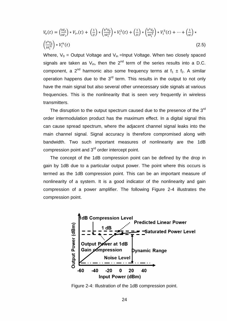
bandwidth. Two such important measures of nonlinearity are the 1dB
compression point and 3rd order intercept point.
The concept of the 1dB compression point can be defined by the drop in
gain by 1dB due to a particular output power. The point where this occurs is
termed as the 1dB compression point. This can be an important measure of
nonlinearity of a system. It is a good indicator of the nonlinearity and gain
compression of a power amplifier. The following Figure 2-4 illustrates the
compression point.
Figure 2-4: Illustration of the 1dB compression point.
25
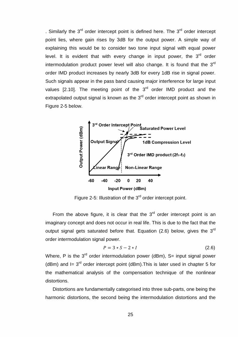
. Similarly the 3rd order intercept point is defined here. The 3rd order intercept
point lies, where gain rises by 3dB for the output power. A simple way of
explaining this would be to consider two tone input signal with equal power
level. It is evident that with every change in input power, the 3rd order
intermodulation product power level will also change. It is found that the 3rd
order IMD product increases by nearly 3dB for every 1dB rise in signal power.
Such signals appear in the pass band causing major interference for large input
values [2.10]. The meeting point of the 3rd order IMD product and the
extrapolated output signal is known as the 3rd order intercept point as shown in
Figure 2-5 below.
Figure 2-5: Illustration of the 3rd order intercept point.
From the above figure, it is clear that the 3rd order intercept point is an
imaginary concept and does not occur in real life. This is due to the fact that the
output signal gets saturated before that. Equation (2.6) below, gives the 3rd
order intermodulation signal power.
. 3 0 1 2 3 (2.6)
Where, P is the 3rd order intermodulation power (dBm), S= input signal power
(dBm) and I= 3rd order intercept point (dBm).This is later used in chapter 5 for
the mathematical analysis of the compensation technique of the nonlinear
distortions.
Distortions are fundamentally categorised into three sub-parts, one being the
harmonic distortions, the second being the intermodulation distortions and the
26
third being the cross-modulation distortions. The harmonic distortions are
generally formed outside the main passband. These lie at multiples of the
fundamental frequency. In order to evaluate the harmonic distortions, the ratio
of the amplitude of the harmonic distortion VHDx and the main signal VM are
evaluated as in equation (2.7), where x denotes the order of the harmonics.
456 789 : (2.7)
The intermodulation distortions contribute to the majority of the nonlinear
distortion. The reason being that, this type of distortion can also appear inside
the passband of the system. This type of distortion is produced when there are
more than one signal component, forming distortion products at combinations of
frequency terms. It is measured by the amplitude ratio of the intermodulation
distortion to the fundamental frequency. The cross modulation distortion is also
very common type of distortion which is formed by the transference of the
amplitude modulation to another signal. The analysis of cross modulation
distortion is carried out by using a single tone signal and another amplitude
modulated signal [2.11] – [2.14]. A detailed discussion will be carried out in
chapter 3 where nonlinear distortion evaluation is mathematically explained.
2.3 Filter Theory
A filter performs by selecting a band of frequencies to pass through while
attenuating the other set. Different filtering techniques are already in place such
as a lowpass filter where only the lower range of frequency is allowed to pass
through while attenuating the rest. A highpass acts in the inverse way as a
lowpass. It only allows the higher range of frequencies to pass through while
attenuating the lower range. A bandpass filter selects a certain band of
frequencies to pass through while attenuating the rest. The bandstop filter is an
inverse of the bandpass filter where a selected range of frequency is attenuated
and the rest is allowed to pass. The allpass filter allows all frequencies to pass
through without exception. A maximum gain of 1 can be reached using a
passive filter. Hence for applications requiring a higher gain, active filter needs
to be chosen. Example of passive filter includes the LC ladder circuit. An
example of an active filter can be a sallen key lowpass filter using operational
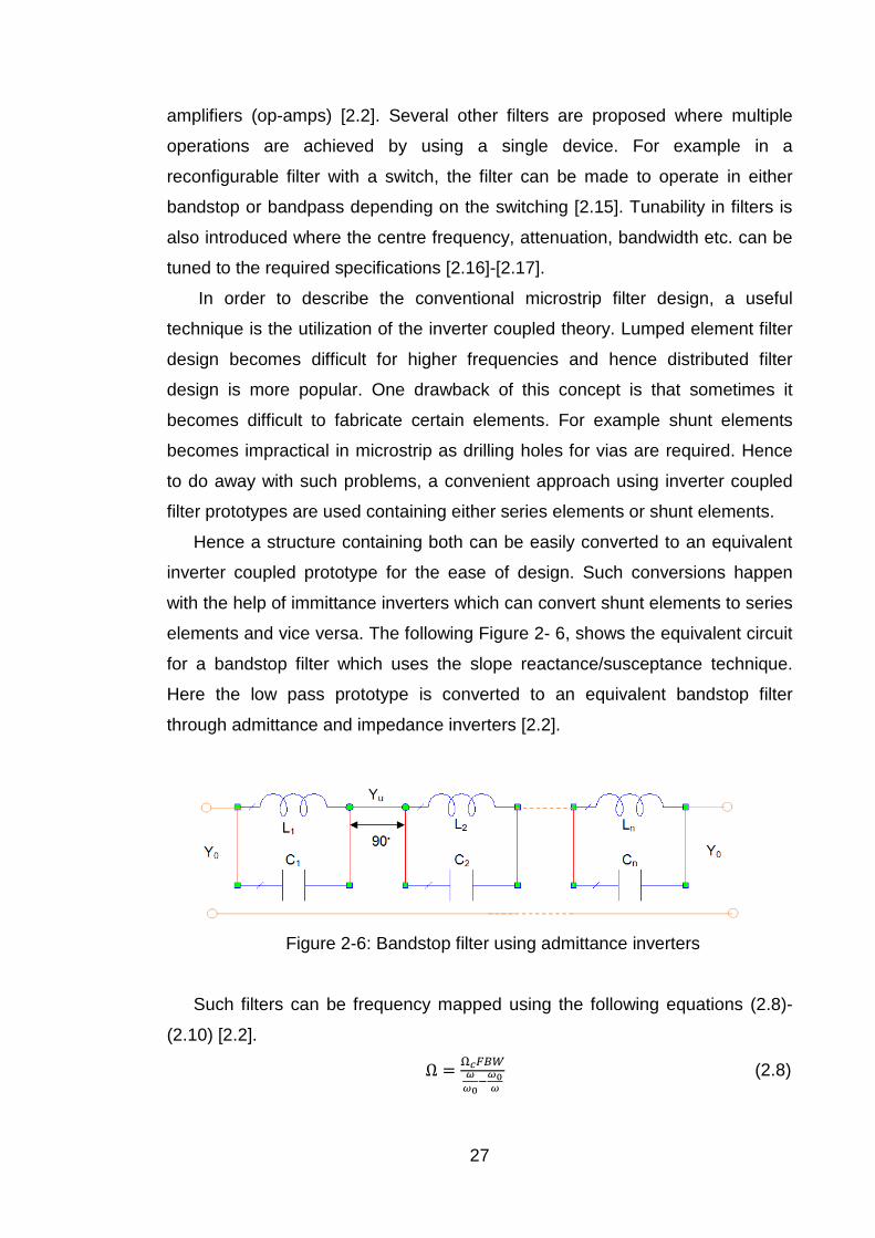
27
amplifiers (op-amps) [2.2]. Several other filters are proposed where multiple
operations are achieved by using a single device. For example in a
reconfigurable filter with a switch, the filter can be made to operate in either
bandstop or bandpass depending on the switching [2.15]. Tunability in filters is
also introduced where the centre frequency, attenuation, bandwidth etc. can be
tuned to the required specifications [2.16]-[2.17].
In order to describe the conventional microstrip filter design, a useful
technique is the utilization of the inverter coupled theory. Lumped element filter
design becomes difficult for higher frequencies and hence distributed filter
design is more popular. One drawback of this concept is that sometimes it
becomes difficult to fabricate certain elements. For example shunt elements
becomes impractical in microstrip as drilling holes for vias are required. Hence
to do away with such problems, a convenient approach using inverter coupled
filter prototypes are used containing either series elements or shunt elements.
Hence a structure containing both can be easily converted to an equivalent
inverter coupled prototype for the ease of design. Such conversions happen
with the help of immittance inverters which can convert shunt elements to series
elements and vice versa. The following Figure 2- 6, shows the equivalent circuit
for a bandstop filter which uses the slope reactance/susceptance technique.
Here the low pass prototype is converted to an equivalent bandstop filter
through admittance and impedance inverters [2.2].
Figure 2-6: Bandstop filter using admittance inverters
Such filters can be frequency mapped using the following equations (2.8)-
(2.10) [2.2].
Ω <=>?@AABAA
(2.8)
28
CDC"&
EE-FG (2.9)
H# IJ# K! L CD
C"& EE!<=>?@ (2.10)
Where the normalized frequency of the lowpass prototype is represented by Ω,
FBW is the fractional bandwidth; ω0 is the centre frequency of the BSF, Yu and
Y0 are the characteristic admittance of the inverter and terminal admittance
respectively, bi represents the slope susceptance and i range from 1 to n, g is
the lowpass prototype element value. Hence the conventional bandstop filters
can be designed using this concept.
The coupled bandstop filters on the other hand requires the use of coupling
coefficient and EM simulation in order to get the correct spacing in between the
resonators. The coupling coefficient can be expressed as K as in equation
(2.11).
M ((BG(((NG( (2.11)
Hence the spacing of the filter is adjusted in order to get the correct value of the
calculated coupling. This way the external quality factor of the filter can also be
calculated [2.2].
Recent demands in higher filtering capabilities with miniaturized size have
led to the development of several new approaches. One such recent concept
uses etching in the ground plane to achieve excellent results with circuit
miniaturization. This technique is widely known as the defected ground structure
[2.18]-[2.20]. One drawback of this kind of structures is the difficulty in modelling
as there are number of parameters which can have effect on the structure such
as the etched design lattice, the number of such lattice etc. On the basis of
DGS, DMS was introduced in order to inculcate some of the benefits of DGS.
DMS modelling can be done by breaking the structure into parts and modelling
individual components. A gap is modelled by a pi network of capacitance.
Similarly a bandgap represents a parallel combination of inductor and capacitor
[2.20]-[2.21]. Chapter 4 details some of the filters that have been designed
using this concept.
29
2.4 References
[2.1] H. Howe, “Microwave Integrated Circuits--An Historical Perspective,"
Microwave Theory and Techniques, IEEE Transactions on, vol.32, no.9,
pp.991-996, Sep 1984.
[2.2] J. Hong and J. Lancaster, Microstrip Filters for RF/Microwave Applications,
New York, John Wiley & Sons, 2001.
[2.3] D. M. Pozar, Microwave engineering, 3rd edition, New York: John Wiley &
Sons, 2004.
[2.4] R.A. Pucel, D.J. Masse and C. P. Hartwig, “Losses in Microstrip”, IEEE
Transactions on Microwave Theory and Techniques, vol. 16, no. 6, pp. 342 -
350, Jun. 1968.
[2.5] K.C. Gupta, R. Garg, I.J. Bahl and P. Bhartia Microstrip Lines and
Slotlines, 2nd edition. Boston: Artech House, 1996.
[2.6] T. Edwards, Foundations for microstrip circuit design. 2nd edition,
Chichester, U.K.: John Wiley & Sons, 1991.
[2.7] S. B. Cohn, “Dissipation Loss in Multiple-Coupled-Resonator Filters”,
Proceedings of the IRE, vol. 47, no. 8, pp. 1342 - 1348, Aug. 1959.
[2.8] R. Garg and I. J. Bahl, "Characteristics of Coupled Microstrip lines," IEEE
Trans. on Microwave Theory and Tech., vol.27, no.7, pp. 700-705, July 1979.
[2.9] A.K. Verma, H. Singh, Nasimuddin, "Closed-form model of shunt
capacitance of microstrip step discontinuity," Microwave Conference
Proceedings, 2005. APMC 2005. Asia-Pacific Conference Proceedings, vol.1,
no., pp.3 pp., 4-7 Dec. 2005.
[2.10] R. G. Meyer, M. J. Shensa, and R. Eschenbach, "Cross modulation and
Intermodulation in amplifiers at high frequencies," IEEE Journal of Solid-State
Circuits, vol. 7, no. 1, pp. 16-23, Feb. 1972.
[2.11] J. Vuolevi and T. Rahkonen, Distortion in RF Power Amplifiers, Artech
House Inc., 2003, ISBN 1580535399.
[2.12] W. Sansen, “Distortion in elementary transistor circuits,” IEEE
Transactions on Circuits and Systems-II: Analog and Digital Signal Processing,
vol. 46, no. 3, pp.315-325, Mar. 1999.
[2.13] S. C. Cripps, RF Power Amplifiers for Wireless Communications, Artech
House Inc., 1999, ISBN 0890069891.
30
[2.14] S. Maas, Nonlinear Microwave and RF Circuits, Artech House Publishers,
2003, ISBN 1580534848.
[2.15] M.F. Karim, G. Yong-Xin, Z.N. Chen and L.C. Ong, "Miniaturized
reconfigurable and switchable filter from UWB to 2.4GHz WLAN using PIN
diodes," Microwave Symposium Digest, 2009. MTT '09. IEEE MTT-S
International, vol., no., pp.509-512, 7-12 June 2009.
[2.16] R. Douglas Jachowski and C. Rauscher, "Frequency-agile bandstop filter
with tunable attenuation," Microwave Symposium Digest, 2009. MTT '09. IEEE
MTT-S International, vol., no., pp.649-652, 7-12 June 2009.
[2.17] I. C. Hunter and J.D. Rhodes, "Electronically Tunable Microwave
Bandstop Filters," Microwave Theory and Techniques, IEEE Transactions on ,
vol.30, no.9, pp.1361,1367, Sep. 1982.
[2.18] Dal Ahn; Jun-Seok Park; Chul-Soo Kim; Juno Kim; Yongxi Qian; T. Itoh ,
"A design of the low-pass filter using the novel microstrip defected ground
structure," Microwave Theory and Techniques, IEEE Transactions on , vol.49,
no.1, pp.86,93, Jan 2001.
[2.19] Jae-Kwan Lee; Young-Sik Kim, "Ultra-Wideband Bandpass Filter With
Improved Upper Stopband Performance Using Defected Ground
Structure," Microwave and Wireless Components Letters, IEEE , vol.20, no.6,
pp.316,318, June 2010.
[2.20] D.Woo, T.Lee, J.Lee, C.Pyo and W.Choi, "Novel U-slot and V-slot DGSs
for bandstop filter with improved Q factor," Microwave Theory and Techniques,
IEEE Transactions on, vol.54, no.6, pp.2840-2847, June 2006.
[2.21] Jong-Sik Lim; Chul-Soo Kim; Young-Taek Lee; Dal Ahn; Sangwook Nam,
"Design of lowpass filters using defected ground structure and compensated
microstrip line," Electronics Letters , vol.38, no.22, pp.1357,1358, 24 Oct 2002.
[2.22] J.A. Tirado-Mendez, H. Jardon-Aguilar, "Comparison of defected ground
structure (DGS) and defected microstrip structure (DGS) behaviour at high
frequencies," Electrical and Electronics Engineering, 2004. (ICEEE). 1st
International Conference on, vol., no., pp.7, 10, 8-10 Sept. 2004.
31
Chapter 3 Nonlinear Distortion in Passive RF Reconfigurable Circuits
This chapter deals with the discussions on nonlinear elements in
transceivers. Such elements can include a power amplifier, a low noise
amplifier, mixers, and reconfigurable or tunable filters. Elements such as
varactor diode, PIN diode, optical switch, MEMS are discussed here due to their
inherent nonlinear property and their use in reconfigurability and tunability of
filters and other devices. Such elements are an important part of RF circuits
today. Hence, applications of such elements in RF circuits namely filters are
also discussed. Due to their inherent nonlinear property, it is imperative to
analyse the effect of nonlinear distortion in the final outputs. Interfering signals
when mixed with main signals are passed through such components; an
increase in nonlinear distortion is noticed. Hence it is imperative to carry out a
complete evaluation of the above components as nonlinear elements to
understand the contribution of nonlinear distortion due to such components on
its own. This can enable an easier analysis in later chapters where such
components in a Tx chain are subjected to interfering signals.
3.1 Non linearity and Intermodulation Distortion
A system can be defined to be an object which gives a response y(t) when a
signal x(t) passes through it. Examples are a transceiver, mixer, filter, power
amplifier etc. A system can be expressed as follows:
y(t) =A[x(t)] (3.1)
Where, y(t) is the response of the system, x(t) is the input signal, A is the
operation performed by the system and t is the independent time variable. A
linear system is defined as one which follows the principle of superposition,
such that the output is a linear combination of two or more outputs of the
32
system when two or more input signals is passed through them. Mathematically
such a system can be defined as:
A[k1x1(t) + k2x2(t)]= k1A[x1(t)] + k2A[x2(t)] (3.2)
Where, k1 and k2 are constants. Hence a system which does not follow the
relationship in (3.2) is defined as nonlinear systems [3.1]-[3.3]. In reality all
systems are nonlinear but act linear within a specified set of conditions. In order
to describe the measure of nonlinearity in RF transceivers it is important to
understand a few terms related to nonlinear distortions. The following
subsections explain the terms related to nonlinear distortion.
3.1.1 Analysis of Nonlinearity
There are several approaches to analyse an electronic device. The four
main methods are listed as follows [3.2]:
1. Load Pulling
2. Scattering Parameter Analysis
3. Time domain (Transient ) Analysis
4. Frequency domain Analysis
Load pulling Analysis is mostly applied to large signal circuits where the
contours of the load impedances are plotted on a Smith Chart. Such a system
requires the use of various impedance loads thus making it practically difficult.
On the other hand, the analysis has little use of the multi-tone input signals
which can significantly decrease the possibility of a wider measurement system.
Scattering parameter analysis (S-parameter) is mainly used to determine the
impendence matching for the source and load of a circuit. The applications of
this analysis are limited in the nonlinear context as the two port S- parameters
itself are linear parameters. These are mostly used for large signal circuits as
well.
Time domain analysis is used for both low and high frequency and digital
circuits. The time domain method of moments is used in solving Maxwell’s
equations. It uses the time domain differential equations to characterise the
circuits. Such analysis is not very compatible with multiple frequency input
signal. It can however be used in large circuits with strong nonlinearities.
33
Frequency domain analysis is applicable to both types of nonlinearity which
are categorised as weakly nonlinear and strongly nonlinear. The power series
and the Volterra series are commonly used in the weakly nonlinear circuit
analysis while the harmonic balance is mostly used for the strongly nonlinear
circuits. This analysis method is very important as it considers the excitation of
circuits due to multi-tone inputs. Due to its simplicity the power series has
become an important tool and will be discussed here to theoretically describe
the nonlinear effects [3.2].
3.1.2 Power Series Analysis and Two Tone Test
The power series is a convenient method of nonlinear analysis especially in
a power amplifier [3.4]-[3.5]. Such series is a polynomial approximation of a
nonlinear transfer function and is given by the following expression:
O # $ O& #& $ O) #) $ + $ O, #, (3.3)
The expression can be written in a more concise form as:
∑ O,#,Q,R (3.4)
Where, = Output Voltage and #=Input Voltage and O,= coefficient at the nth
term. A power series as described by (3.4) assumes a memoryless effect which
means that there is no effect on the final output due to previous input
excitations. But in reality, circuits having energy storage elements such as
inductors and capacitors affect the output signal not only due to the current
input excitations but also previous excitations. This is also known as the
memory effect. This changes the standard equation in (3.4) and a new variable
needs to be added in order to cater for the memory effect. This is done by using
a time constant in the equation (3.4) which can now be written as follows [3.6]:
∑ O,#,Q,R 1 , (3.5)
This expression can be expanded further as:
O # 1 $ O& #& 1 & $ O) #) 1 )
$ + $ O, #, 1 , (3.6)
Hence when amplitude modulated and phase modulated signal is passed
through such a system represented by the above equation (3.6), it results in
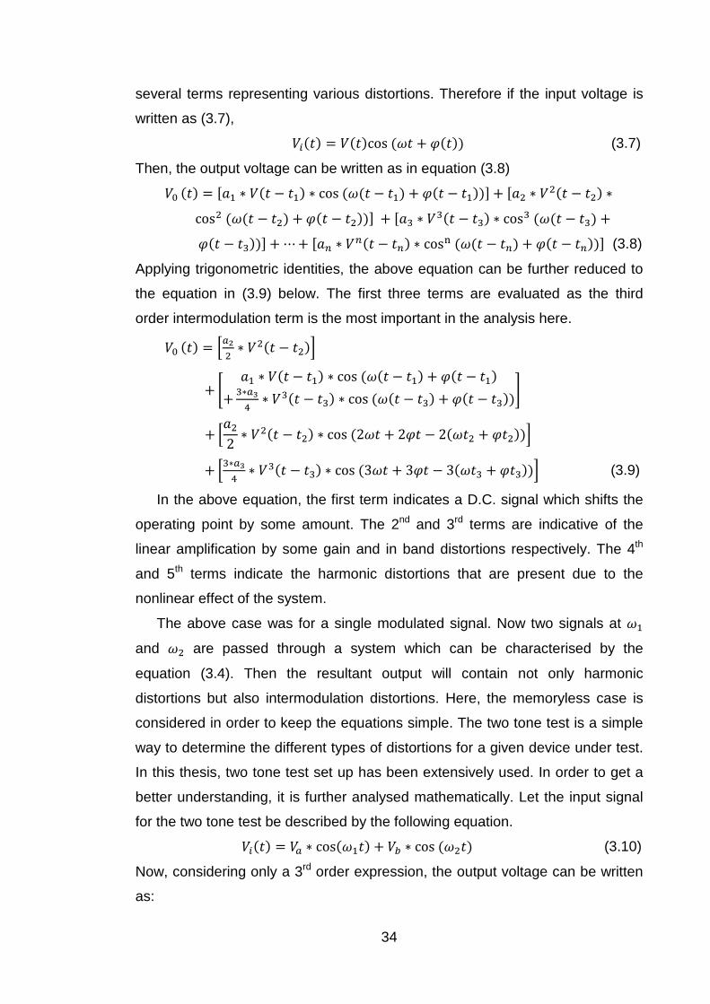
34
several terms representing various distortions. Therefore if the input voltage is
written as (3.7),
# cos I $ V (3.7)
Then, the output voltage can be written as in equation (3.8)
WO 1 cos I 1 $ V 1 X $ WO& & 1 & cos& I 1 & $ V 1 &X $ WO) ) 1 ) cos) I 1 ) $ V 1 )X $ + $ WO, , 1 , cosY I 1 , $ V 1 ,X (3.8)
Applying trigonometric identities, the above equation can be further reduced to
the equation in (3.9) below. The first three terms are evaluated as the third
order intermodulation term is the most important in the analysis here.
Z[(& & 1 &\
$ ] O 1 cos I 1 $ V 1 $ )[*
^ ) 1 ) cos I 1 ) $ V 1 )_ $ ZO&2 & 1 & cos 2I $ 2V 1 2I& $ V&\
$ Z)[*^ ) 1 ) cos 3I $ 3V 1 3I) $ V)\ (3.9)
In the above equation, the first term indicates a D.C. signal which shifts the
operating point by some amount. The 2nd and 3rd terms are indicative of the
linear amplification by some gain and in band distortions respectively. The 4th
and 5th terms indicate the harmonic distortions that are present due to the
nonlinear effect of the system.
The above case was for a single modulated signal. Now two signals at I
and I& are passed through a system which can be characterised by the
equation (3.4). Then the resultant output will contain not only harmonic
distortions but also intermodulation distortions. Here, the memoryless case is
considered in order to keep the equations simple. The two tone test is a simple
way to determine the different types of distortions for a given device under test.
In this thesis, two tone test set up has been extensively used. In order to get a
better understanding, it is further analysed mathematically. Let the input signal
for the two tone test be described by the following equation.
# [ cosI $ cos I& (3.10)
Now, considering only a 3rd order expression, the output voltage can be written
as:

35
[( a(& $ [( b(&
$ O[ $ )[* a*^ $ )[* a b(& " cosI $ O $ )[* b*^ $ )[* b a(
& " cosI&
$ [( a(& cos2I $ [( b(& cos2I& $ [* a*
^ cos3I $ [* b*^ cos3I&
$O&[ cosI 1 I& $ O&[ cosI $ I& $ [* a( b^ Wcos2I 1
I& $ cos2I$ I& X $ [* b( a^ c cos2I& 1 I $ cos2I&$ I d (3.11)
The components of the above equations includes the D.C. signal (the
constant terms), harmonics of the fundamental frequency
(I, I&, 2I, 2I&, 3I, 3I&) and the intermodulation distortions arising due to the
mixing of the two frequencies (IOfg I&. Hence the second order
intermodulation terms are denoted by (I 1 I& Ofg I $ I&. The third order
intermodulation terms are denoted by (2I 1 I& , 2I $ I&, I 1 2I& Ofg I $2I&).The following figure is an illustration to show the intermodulation
distortions.
Figure 3-1 : Illustration of nonlinear effect showing various distortion products.
Most of the harmonics and D.C. components can be easily filtered out as
they are mostly out-of band distortions. On the other hand, the odd order
intermodulation products formed due to the mixing of two or more frequencies
fall in the in-band region causing significant distortions in the output level as it
becomes difficult to filter out such components. The power level of the 3rd order
intermodulation distortion is found to be the highest and most significant and
Nonlinear System f1 f2
f1 f2
2f1-f2 2f2-f1
3f1
f2-f1
2f1 - f2, 2f2 - f1, 2f1 + f2, 2f2 + f1
3rd Oder Inter Modulation Product
f2 - f1 and f 2 + f1
2nd Oder Inter Modulation Product
f1 and f 2 fundamental frequency
2f1 2f2
f2+f1 2f2+f1
2f1+f2
3f2
2f1, 2f2, 3f1 and 3f 2
2nd and 3 rd Harmonic
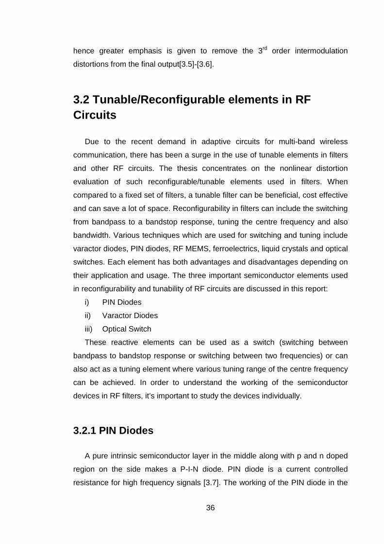
36
hence greater emphasis is given to remove the 3rd order intermodulation
distortions from the final output[3.5]-[3.6].
3.2 Tunable/Reconfigurable elements in RF Circuits
Due to the recent demand in adaptive circuits for multi-band wireless
communication, there has been a surge in the use of tunable elements in filters
and other RF circuits. The thesis concentrates on the nonlinear distortion
evaluation of such reconfigurable/tunable elements used in filters. When
compared to a fixed set of filters, a tunable filter can be beneficial, cost effective
and can save a lot of space. Reconfigurability in filters can include the switching
from bandpass to a bandstop response, tuning the centre frequency and also
bandwidth. Various techniques which are used for switching and tuning include
varactor diodes, PIN diodes, RF MEMS, ferroelectrics, liquid crystals and optical
switches. Each element has both advantages and disadvantages depending on
their application and usage. The three important semiconductor elements used
in reconfigurability and tunability of RF circuits are discussed in this report:
i) PIN Diodes
ii) Varactor Diodes
iii) Optical Switch
These reactive elements can be used as a switch (switching between
bandpass to bandstop response or switching between two frequencies) or can
also act as a tuning element where various tuning range of the centre frequency
can be achieved. In order to understand the working of the semiconductor
devices in RF filters, it’s important to study the devices individually.
3.2.1 PIN Diodes
A pure intrinsic semiconductor layer in the middle along with p and n doped
region on the side makes a P-I-N diode. PIN diode is a current controlled
resistance for high frequency signals [3.7]. The working of the PIN diode in the

forward biased condition depends on the holes and electrons which are injected
from the P and N region to the I region. Since the charges do not
immediately this is stored in it [
forward resistance, which is varied because of the modulation of this stored
charge by the microwave signal [3.9
stored charge in the
Where, IF is denoted as the forward bias current and
carrier lifetime. The total series resistance can be expressed as an inverse
proportion of the total charge
also result in the variation
and leads to distortions
analysis shown in
diode is much lesser for small RF
BAP65-02, a s
nonlinear effects [3.11
order to switch it from bandpass to bandstop response
circuits for the PIN
Figure 3-2. The ON state can be modelled by a simple series resistance R
a parasitic inductance L
denoted by a capacitance C and shunt loss element R
represents parasitic inductance. In the ON state, the forward resistance is low,
while in the off state the resistance tends be much higher. This is how the
diode acts a switch in RF circuits [
(a)
Figure 3-2: Equivalent circuits for (a) forward biased (b) r
37
forward biased condition depends on the holes and electrons which are injected
from the P and N region to the I region. Since the charges do not
immediately this is stored in it [3.8]. Non linearity arises due to the time varying
forward resistance, which is varied because of the modulation of this stored
icrowave signal [3.9]. In order to mathematically define the
charge in the PIN diode, we consider Qs as the stored
Qi Ikτ is denoted as the forward bias current and τ is the minority charge
carrier lifetime. The total series resistance can be expressed as an inverse
proportion of the total charge QS. Hence any variation in the stored charge will
also result in the variation of the resistance. This makes the
distortions in the output spectrum [3.7].
analysis shown in [3.7], [3.9], and [3.10] proved that the distortion due a
diode is much lesser for small RF signals as compared to varactor diode
silicon PIN diode has been used in order to analy
nonlinear effects [3.11]. These diodes are further used in filters
order to switch it from bandpass to bandstop response [3.12
PIN diode for both forward bias and reverse bias
2. The ON state can be modelled by a simple series resistance R
a parasitic inductance LS. The OFF state or the reverse biased condition can be
capacitance C and shunt loss element RL. The inductance L
represents parasitic inductance. In the ON state, the forward resistance is low,
while in the off state the resistance tends be much higher. This is how the
diode acts a switch in RF circuits [3.13].
(a)
2: Equivalent circuits for (a) forward biased (b) r
PIN diode.
forward biased condition depends on the holes and electrons which are injected
from the P and N region to the I region. Since the charges do not recombine
]. Non linearity arises due to the time varying
forward resistance, which is varied because of the modulation of this stored
In order to mathematically define the
as the stored charge [3.7].
(3.12)
τ is the minority charge
carrier lifetime. The total series resistance can be expressed as an inverse
. Hence any variation in the stored charge will
e resistance. This makes the PIN diode nonlinear
]. Nonlinear distortion
that the distortion due a PIN
ompared to varactor diode.
diode has been used in order to analyse the
]. These diodes are further used in filters as switches in
[3.12].The equivalent
diode for both forward bias and reverse bias are given in
2. The ON state can be modelled by a simple series resistance RS and
. The OFF state or the reverse biased condition can be
. The inductance LP
represents parasitic inductance. In the ON state, the forward resistance is low,
while in the off state the resistance tends be much higher. This is how the PIN
(b)
2: Equivalent circuits for (a) forward biased (b) reversed biased for
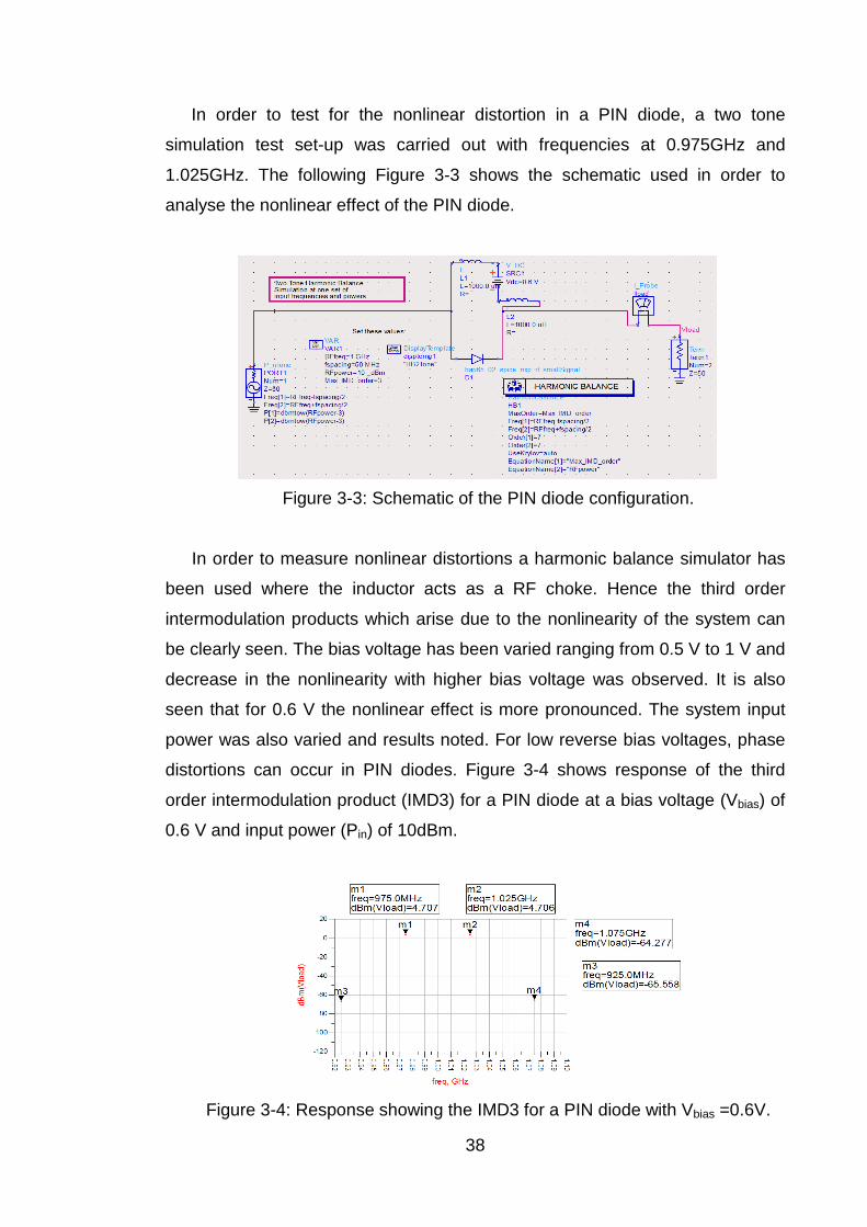
38
In order to test for the nonlinear distortion in a PIN diode, a two tone
simulation test set-up was carried out with frequencies at 0.975GHz and
1.025GHz. The following Figure 3-3 shows the schematic used in order to
analyse the nonlinear effect of the PIN diode.
Figure 3-3: Schematic of the PIN diode configuration.
In order to measure nonlinear distortions a harmonic balance simulator has
been used where the inductor acts as a RF choke. Hence the third order
intermodulation products which arise due to the nonlinearity of the system can
be clearly seen. The bias voltage has been varied ranging from 0.5 V to 1 V and
decrease in the nonlinearity with higher bias voltage was observed. It is also
seen that for 0.6 V the nonlinear effect is more pronounced. The system input
power was also varied and results noted. For low reverse bias voltages, phase
distortions can occur in PIN diodes. Figure 3-4 shows response of the third
order intermodulation product (IMD3) for a PIN diode at a bias voltage (Vbias) of
0.6 V and input power (Pin) of 10dBm.
Figure 3-4: Response showing the IMD3 for a PIN diode with Vbias =0.6V.

39
As can be seen from the above figure, the third order intermodulation
product appears at 2f1-f2 (925MHz) and 2f2-f1 (1.975GHz) at marker m3 and m4,
and has a power level of -64dBm. The main tone output signals occur at f1 and
f2 at 975MHz and 1.025GHz. The distortion level measured is relatively low but
it is still not a desirable property in a filter, due to the filter’s utilization in
removing distortions and unwanted signal.
The PIN diode shows distortions in both ON and OFF state. In the OFF
state, the distortion is generated due to the capacitance modulation [3.14].
Figure 3-5 shows the effects of change in output power (Pout) with respect to
change in input power (Pin) at the bias voltage of 0.6 V. It also shows the
change of the higher 3rd order intermodulation product (IMD3) at frequency
1.975GHz with respect to the input power (Pin) which ranges from -10 to
20dBm.
-10 0 10 20Pin(dBm)
-140
-120
-100
-80
-60
-40
3rd
Od
er I
MD
(d
Bm
)
-16
-12
-8
-4
0
4
8
Po
ut(
dB
m)
3rd Order IMDPout
Figure 3-5: Variation in Pout and IMD3 with reference to different Pin when
Vbias = 0.6V or ON stage.
As can be seen from Figure 3-5, the Pout curve is not linear. A saturation
point is seen around -5dBm for the input power Pin. For higher input power
levels, the third order intermodulation is much higher reaching to as high as -
40dBm which can cause problem in many RF applications.
40
3.2.2 Varactor Diodes
As compared to the PIN diode, a varactor diode’s main mode of operation is
as a variable capacitor, which can change the centre frequency of a filter. Since
it works in reverse bias condition, there is no current flow, but the capacitance is
varied by the bias voltage. The changing thickness of the depletion layer that is
formed in the diode gives rise to the capacitance [3.15]. In order to describe this
mathematically we use the following equation (3.13).
Jm noNpqrns
tn (3.13)
Where, Cj0 is defined as the junction capacitance at zero bias, vR is the voltage
for the reverse bias, mj is the doping coefficient and Vj is the junction potential.
The nonlinearity of the varactor diode arises because of the modulation of the
capacitance by the RF signal [3.16]. The capacitance is also a nonlinear
function of the bias voltage as can be seen from the equation (3.13). For lower
bias voltages, when the RF signal is comparable to the D.C. biasing, the
distortions seen are more severe [3.15], [3.16] and [3.17]. An equivalent circuit
model for the varactor is shown in Figure 3-6.
Figure 3-6: Equivalent circuit model for varactor diode.
The variable junction capacitance Cj and the junction resistance Rs are
both functions of the junction voltage. The parasitic capacitance Cp and
inductance Lp are also modelled in the equivalent circuit. An ADS harmonic
balance simulation is carried out on a varactor model to analyse nonlinearity, as
it contributes towards further distortions in the output signal. A two tone test was
for the commercial varactor diode model NXP BB135 with different sets of input
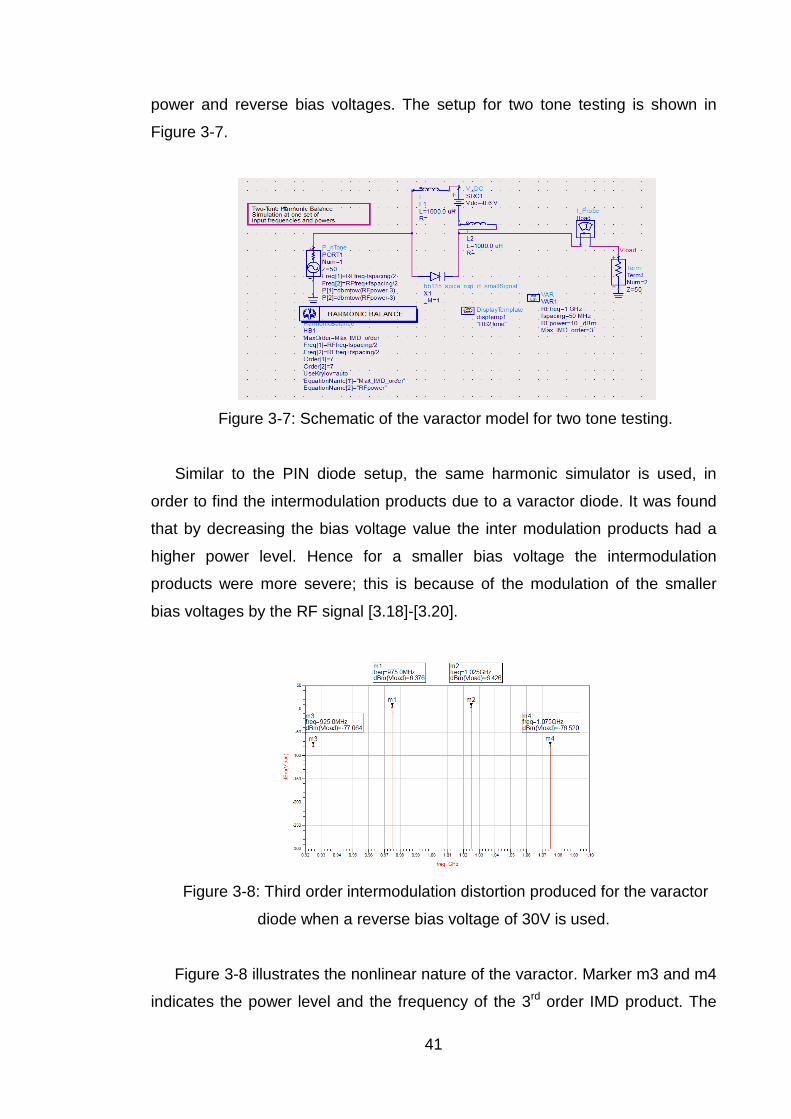
41
power and reverse bias voltages. The setup for two tone testing is shown in
Figure 3-7.
Figure 3-7: Schematic of the varactor model for two tone testing.
Similar to the PIN diode setup, the same harmonic simulator is used, in
order to find the intermodulation products due to a varactor diode. It was found
that by decreasing the bias voltage value the inter modulation products had a
higher power level. Hence for a smaller bias voltage the intermodulation
products were more severe; this is because of the modulation of the smaller
bias voltages by the RF signal [3.18]-[3.20].
Figure 3-8: Third order intermodulation distortion produced for the varactor
diode when a reverse bias voltage of 30V is used.
Figure 3-8 illustrates the nonlinear nature of the varactor. Marker m3 and m4
indicates the power level and the frequency of the 3rd order IMD product. The
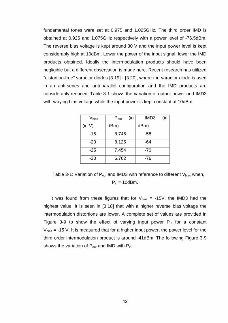
42
fundamental tones were set at 0.975 and 1.025GHz. The third order IMD is
obtained at 0.925 and 1.075GHz respectively with a power level of -76.5dBm.
The reverse bias voltage is kept around 30 V and the input power level is kept
considerably high at 10dBm. Lower the power of the input signal, lower the IMD
products obtained. Ideally the intermodulation products should have been
negligible but a different observation is made here. Recent research has utilized
“distortion-free” varactor diodes [3.19] - [3.20], where the varactor diode is used
in an anti-series and anti-parallel configuration and the IMD products are
considerably reduced. Table 3-1 shows the variation of output power and IMD3
with varying bias voltage while the input power is kept constant at 10dBm:
Vbias
(in V)
Pout (in
dBm)
IMD3 (in
dBm)
-15 8.745 -58
-20 8.125 -64
-25 7.454 -70
-30 6.762 -76
Table 3-1: Variation of Pout and IMD3 with reference to different Vbias when,
Pin = 10dBm.
It was found from these figures that for Vbias = -15V, the IMD3 had the
highest value. It is seen in [3.18] that with a higher reverse bias voltage the
intermodulation distortions are lower. A complete set of values are provided in
Figure 3-9 to show the effect of varying input power Pin for a constant
Vbias = -15 V. It is measured that for a higher input power, the power level for the
third order intermodulation product is around -41dBm. The following Figure 3-9
shows the variation of Pout and IMD with Pin.

43
-20 -10 0 10 20Pin(dBm)
-30
-20
-10
0
10
20
Po
ut(
dB
m)
-100
-80
-60
-40
IMD
3(dB
m)
PoutIMD
Figure 3-9: Variation in Pout and IMD3 with reference to different Pin, for
Vbias = -15V.
The above figure shows the variation of Pout and IMD3 to the Pin. The plot for
the output power sees a slight saturation around 7-10dBm. The IMD increases
with the power level reaching -40dBm for a Pin = 20dBm.
3.2.3 Optical Switch
In recent years, photoconductive silicon switches (PSS) are used as a
switch in RF circuits. These switches are optically controlled and can be used in
tuning circuits because of the change in their conductivity when subjected to
optical illumination. The light should have a particular wavelength and flux
density in order to change the conductivity of the silicon switch [3.19]-[3.20].The
switches used here to model distortions have been diced from silicon wafers
having a very high resistivity (>6000Ωcm) . In the original form, the silicon dices
acts as insulators but on illumination, the switches starts conducting.
Phosphorus is often used to dope the n-type switches to increase the static
conductivity [3.21]-[3.25].
The equivalent circuit for an optical switch can be modelled as given in
Figure 3-10. Experimental data in [3.23]-[3.25] suggests that in the ON state,
the values of RG and RS decrease while CG and CS increase. Additionally in
[3.24], an overall insertion-loss of around 0.68dB was found in the ON state
(under an illumination of 200mW optical power) of a single silicon switch while
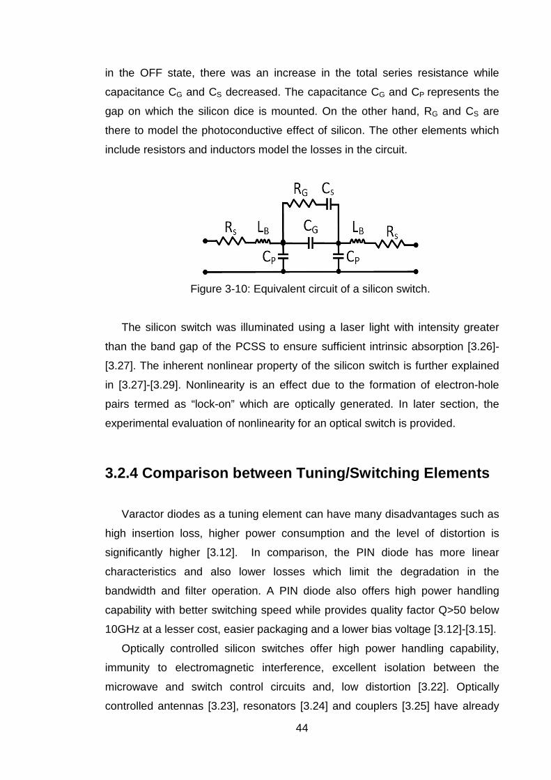
44
in the OFF state, there was an increase in the total series resistance while
capacitance CG and CS decreased. The capacitance CG and CP represents the
gap on which the silicon dice is mounted. On the other hand, RG and CS are
there to model the photoconductive effect of silicon. The other elements which
include resistors and inductors model the losses in the circuit.
Figure 3-10: Equivalent circuit of a silicon switch.
The silicon switch was illuminated using a laser light with intensity greater
than the band gap of the PCSS to ensure sufficient intrinsic absorption [3.26]-
[3.27]. The inherent nonlinear property of the silicon switch is further explained
in [3.27]-[3.29]. Nonlinearity is an effect due to the formation of electron-hole
pairs termed as “lock-on” which are optically generated. In later section, the
experimental evaluation of nonlinearity for an optical switch is provided.
3.2.4 Comparison between Tuning/Switching Elements
Varactor diodes as a tuning element can have many disadvantages such as
high insertion loss, higher power consumption and the level of distortion is
significantly higher [3.12]. In comparison, the PIN diode has more linear
characteristics and also lower losses which limit the degradation in the
bandwidth and filter operation. A PIN diode also offers high power handling
capability with better switching speed while provides quality factor Q>50 below
10GHz at a lesser cost, easier packaging and a lower bias voltage [3.12]-[3.15].
Optically controlled silicon switches offer high power handling capability,
immunity to electromagnetic interference, excellent isolation between the
microwave and switch control circuits and, low distortion [3.22]. Optically
controlled antennas [3.23], resonators [3.24] and couplers [3.25] have already
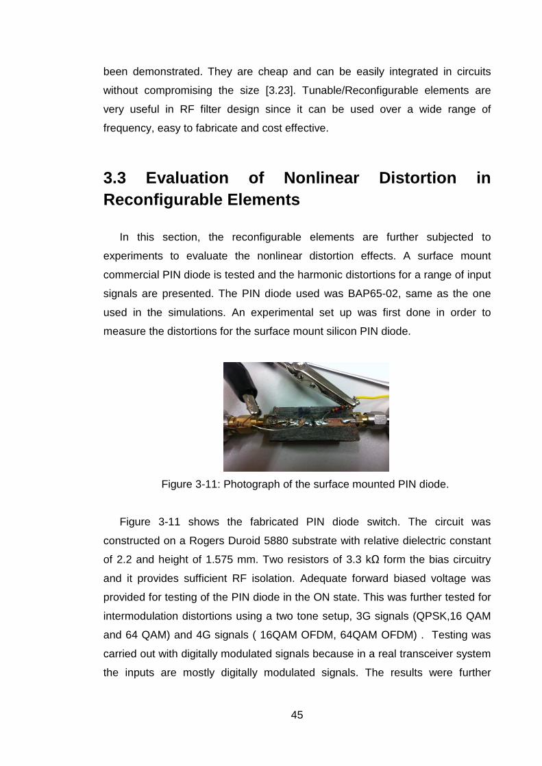
45
been demonstrated. They are cheap and can be easily integrated in circuits
without compromising the size [3.23]. Tunable/Reconfigurable elements are
very useful in RF filter design since it can be used over a wide range of
frequency, easy to fabricate and cost effective.
3.3 Evaluation of Nonlinear Distortion in Reconfigurable Elements
In this section, the reconfigurable elements are further subjected to
experiments to evaluate the nonlinear distortion effects. A surface mount
commercial PIN diode is tested and the harmonic distortions for a range of input
signals are presented. The PIN diode used was BAP65-02, same as the one
used in the simulations. An experimental set up was first done in order to
measure the distortions for the surface mount silicon PIN diode.
Figure 3-11: Photograph of the surface mounted PIN diode.
Figure 3-11 shows the fabricated PIN diode switch. The circuit was
constructed on a Rogers Duroid 5880 substrate with relative dielectric constant
of 2.2 and height of 1.575 mm. Two resistors of 3.3 kΩ form the bias circuitry
and it provides sufficient RF isolation. Adequate forward biased voltage was
provided for testing of the PIN diode in the ON state. This was further tested for
intermodulation distortions using a two tone setup, 3G signals (QPSK,16 QAM
and 64 QAM) and 4G signals ( 16QAM OFDM, 64QAM OFDM) . Testing was
carried out with digitally modulated signals because in a real transceiver system
the inputs are mostly digitally modulated signals. The results were further
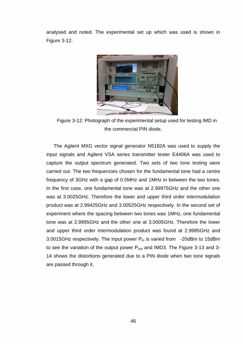
46
analysed and noted. The experimental set up which was used is shown in
Figure 3-12.
Figure 3-12: Photograph of the experimental setup used for testing IMD in
the commercial PIN diode.
The Agilent MXG vector signal generator N5182A was used to supply the
input signals and Agilent VSA series transmitter tester E4406A was used to
capture the output spectrum generated. Two sets of two tone testing were
carried out. The two frequencies chosen for the fundamental tone had a centre
frequency of 3GHz with a gap of 0.5MHz and 1MHz in between the two tones.
In the first case, one fundamental tone was at 2.99975GHz and the other one
was at 3.0025GHz. Therefore the lower and upper third order intermodulation
product was at 2.99425GHz and 3.00525GHz respectively. In the second set of
experiment where the spacing between two tones was 1MHz, one fundamental
tone was at 2.9995GHz and the other one at 3.0005GHz. Therefore the lower
and upper third order intermodulation product was found at 2.9985GHz and
3.0015GHz respectively. The input power Pin is varied from -20dBm to 15dBm
to see the variation of the output power Pout and IMD3. The Figure 3-13 and 3-
14 shows the distortions generated due to a PIN diode when two tone signals
are passed through it.
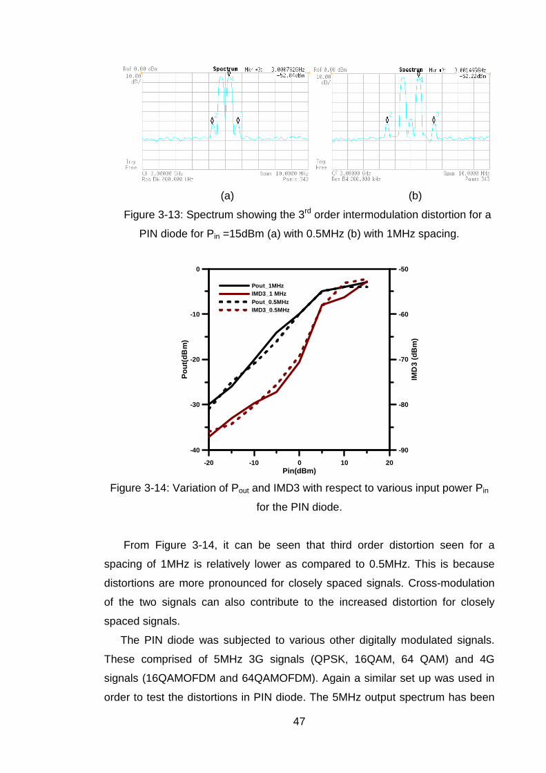
Figure 3-13: Spectrum showing the 3
PIN diode for
-40
-30
-20
-10
0
Pou
t(dB
m)
Figure 3-14: Variation of P
From Figure 3
spacing of 1MHz is relatively lower as compared to 0.5
distortions are more pronounced fo
of the two signals can also contribute to the increased distortion for closely
spaced signals.
The PIN diode was subje
These comprised of 5MHz 3G signals (QPSK, 16QAM, 64 QAM) and 4G
signals (16QAMOFDM and 64QAMOFDM). Again a similar set up was used in
order to test the distortions in
47
(a) (b)
13: Spectrum showing the 3rd order intermodulation
diode for Pin =15dBm (a) with 0.5MHz (b) with 1MHz
-20 -10 0 10 20Pin(dBm)
-40
-30
-20
-10
0
Pout_1MHzIMD3_1 MHzPout_0.5MHzIMD3_0.5MHz
14: Variation of Pout and IMD3 with respect to various input power
for the PIN diode.
From Figure 3-14, it can be seen that third order distortion seen for a
is relatively lower as compared to 0.5MHz
distortions are more pronounced for closely spaced signals. Cross
of the two signals can also contribute to the increased distortion for closely
diode was subjected to various other digitally modulated signals.
These comprised of 5MHz 3G signals (QPSK, 16QAM, 64 QAM) and 4G
signals (16QAMOFDM and 64QAMOFDM). Again a similar set up was used in
order to test the distortions in PIN diode. The 5MHz output spectrum ha
(a) (b)
ntermodulation distortion for a
MHz spacing.
-90
-80
-70
-60
-50
IMD
3 (d
Bm
)
and IMD3 with respect to various input power Pin
14, it can be seen that third order distortion seen for a
MHz. This is because
r closely spaced signals. Cross-modulation
of the two signals can also contribute to the increased distortion for closely
cted to various other digitally modulated signals.
These comprised of 5MHz 3G signals (QPSK, 16QAM, 64 QAM) and 4G
signals (16QAMOFDM and 64QAMOFDM). Again a similar set up was used in
diode. The 5MHz output spectrum has been
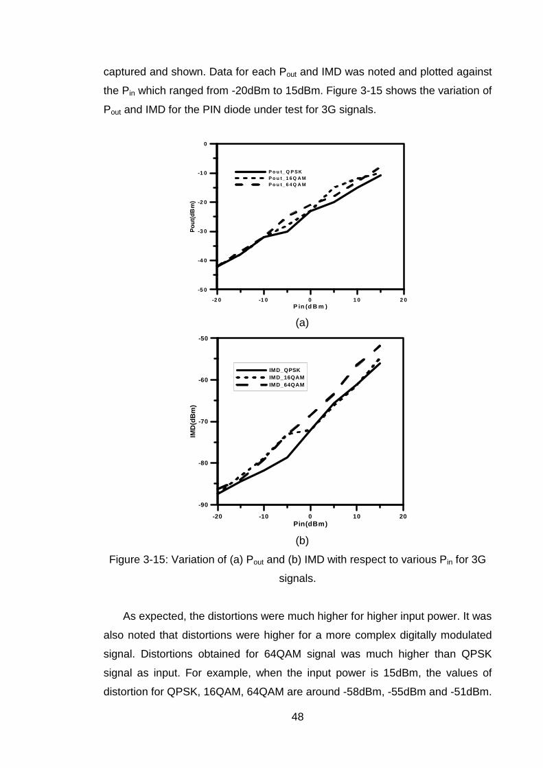
48
captured and shown. Data for each Pout and IMD was noted and plotted against
the Pin which ranged from -20dBm to 15dBm. Figure 3-15 shows the variation of
Pout and IMD for the PIN diode under test for 3G signals.
-2 0 -1 0 0 1 0 2 0P in (d B m )
-5 0
-4 0
-3 0
-2 0
-1 0
0
Pou
t(dB
m)
P o u t_ Q P S KP o u t_ 1 6 Q A MP o u t_ 6 4 Q A M
(a)
-20 -10 0 10 20Pin(dBm)
-90
-80
-70
-60
-50
IMD
(dB
m)
IMD_QPSKIMD_16QAMIMD_64QAM
(b)
Figure 3-15: Variation of (a) Pout and (b) IMD with respect to various Pin for 3G
signals.
As expected, the distortions were much higher for higher input power. It was
also noted that distortions were higher for a more complex digitally modulated
signal. Distortions obtained for 64QAM signal was much higher than QPSK
signal as input. For example, when the input power is 15dBm, the values of
distortion for QPSK, 16QAM, 64QAM are around -58dBm, -55dBm and -51dBm.
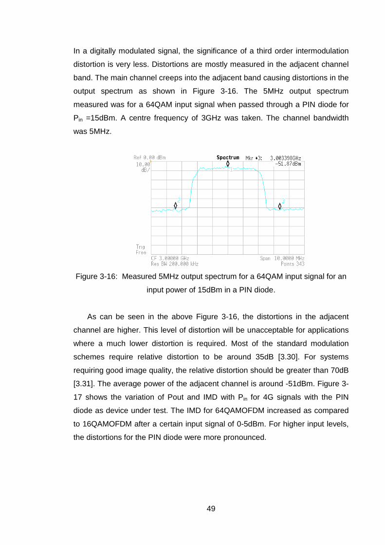
49
In a digitally modulated signal, the significance of a third order intermodulation
distortion is very less. Distortions are mostly measured in the adjacent channel
band. The main channel creeps into the adjacent band causing distortions in the
output spectrum as shown in Figure 3-16. The 5MHz output spectrum
measured was for a 64QAM input signal when passed through a PIN diode for
Pin =15dBm. A centre frequency of 3GHz was taken. The channel bandwidth
was 5MHz.
Figure 3-16: Measured 5MHz output spectrum for a 64QAM input signal for an
input power of 15dBm in a PIN diode.
As can be seen in the above Figure 3-16, the distortions in the adjacent
channel are higher. This level of distortion will be unacceptable for applications
where a much lower distortion is required. Most of the standard modulation
schemes require relative distortion to be around 35dB [3.30]. For systems
requiring good image quality, the relative distortion should be greater than 70dB
[3.31]. The average power of the adjacent channel is around -51dBm. Figure 3-
17 shows the variation of Pout and IMD with Pin for 4G signals with the PIN
diode as device under test. The IMD for 64QAMOFDM increased as compared
to 16QAMOFDM after a certain input signal of 0-5dBm. For higher input levels,
the distortions for the PIN diode were more pronounced.
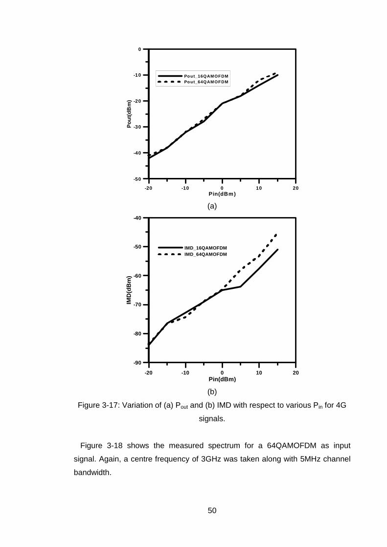
50
-20 -10 0 10 20Pin(dBm)
-50
-40
-30
-20
-10
0
Pou
t(dB
m)
Pout_16QAMOFDMPout_64QAMOFDM
(a)
-20 -10 0 10 20Pin(dBm)
-90
-80
-70
-60
-50
-40
IMD
(dB
m)
IMD_16QAMOFDMIMD_64QAMOFDM
(b)
Figure 3-17: Variation of (a) Pout and (b) IMD with respect to various Pin for 4G
signals.
Figure 3-18 shows the measured spectrum for a 64QAMOFDM as input
signal. Again, a centre frequency of 3GHz was taken along with 5MHz channel
bandwidth.
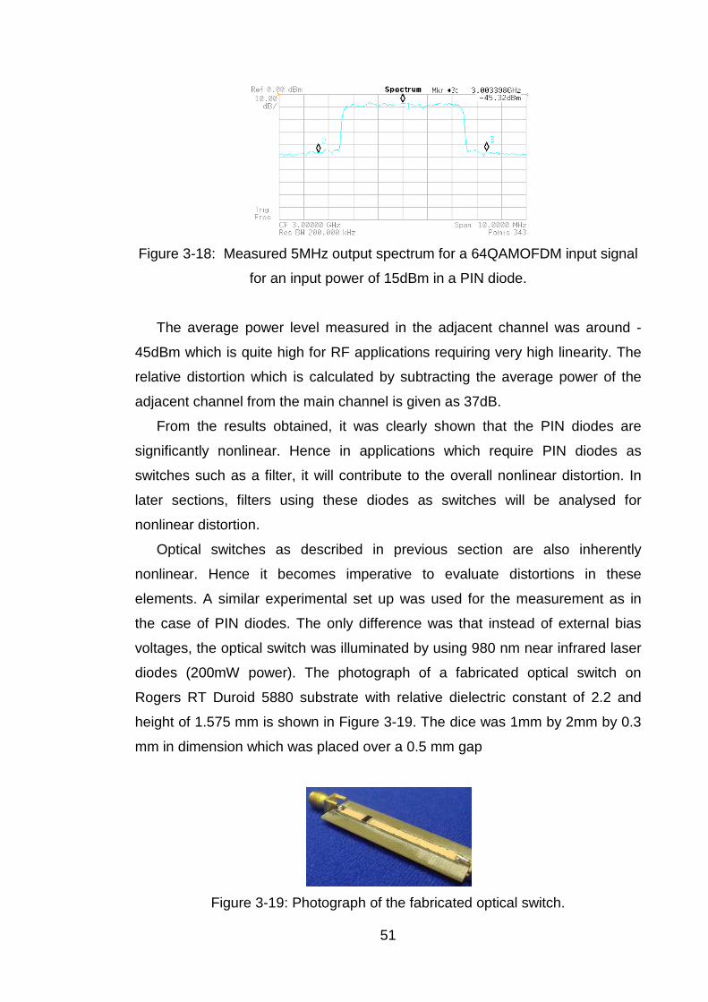
51
Figure 3-18: Measured 5MHz output spectrum for a 64QAMOFDM input signal
for an input power of 15dBm in a PIN diode.
The average power level measured in the adjacent channel was around -
45dBm which is quite high for RF applications requiring very high linearity. The
relative distortion which is calculated by subtracting the average power of the
adjacent channel from the main channel is given as 37dB.
From the results obtained, it was clearly shown that the PIN diodes are
significantly nonlinear. Hence in applications which require PIN diodes as
switches such as a filter, it will contribute to the overall nonlinear distortion. In
later sections, filters using these diodes as switches will be analysed for
nonlinear distortion.
Optical switches as described in previous section are also inherently
nonlinear. Hence it becomes imperative to evaluate distortions in these
elements. A similar experimental set up was used for the measurement as in
the case of PIN diodes. The only difference was that instead of external bias
voltages, the optical switch was illuminated by using 980 nm near infrared laser
diodes (200mW power). The photograph of a fabricated optical switch on
Rogers RT Duroid 5880 substrate with relative dielectric constant of 2.2 and
height of 1.575 mm is shown in Figure 3-19. The dice was 1mm by 2mm by 0.3
mm in dimension which was placed over a 0.5 mm gap
Figure 3-19: Photograph of the fabricated optical switch.
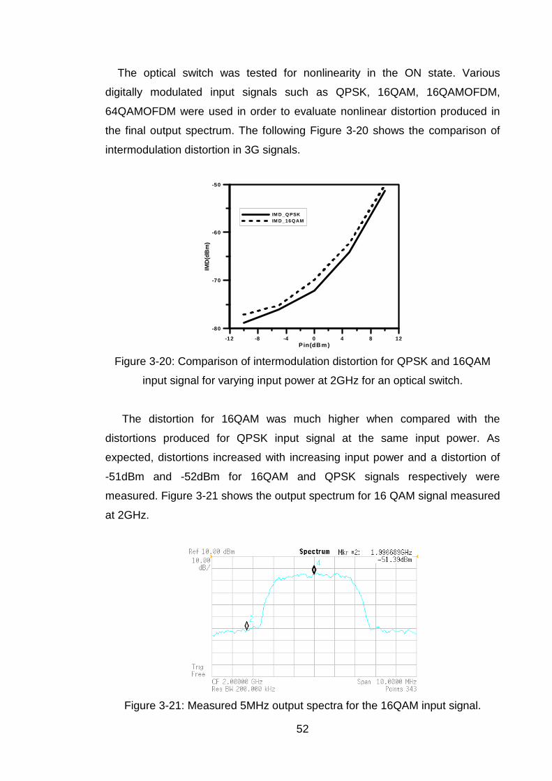
52
The optical switch was tested for nonlinearity in the ON state. Various
digitally modulated input signals such as QPSK, 16QAM, 16QAMOFDM,
64QAMOFDM were used in order to evaluate nonlinear distortion produced in
the final output spectrum. The following Figure 3-20 shows the comparison of
intermodulation distortion in 3G signals.
-12 -8 -4 0 4 8 12Pin(dBm )
-80
-70
-60
-50
IMD
(dB
m)
IM D_Q PSKIM D_16QAM
Figure 3-20: Comparison of intermodulation distortion for QPSK and 16QAM
input signal for varying input power at 2GHz for an optical switch.
The distortion for 16QAM was much higher when compared with the
distortions produced for QPSK input signal at the same input power. As
expected, distortions increased with increasing input power and a distortion of
-51dBm and -52dBm for 16QAM and QPSK signals respectively were
measured. Figure 3-21 shows the output spectrum for 16 QAM signal measured
at 2GHz.
Figure 3-21: Measured 5MHz output spectra for the 16QAM input signal.
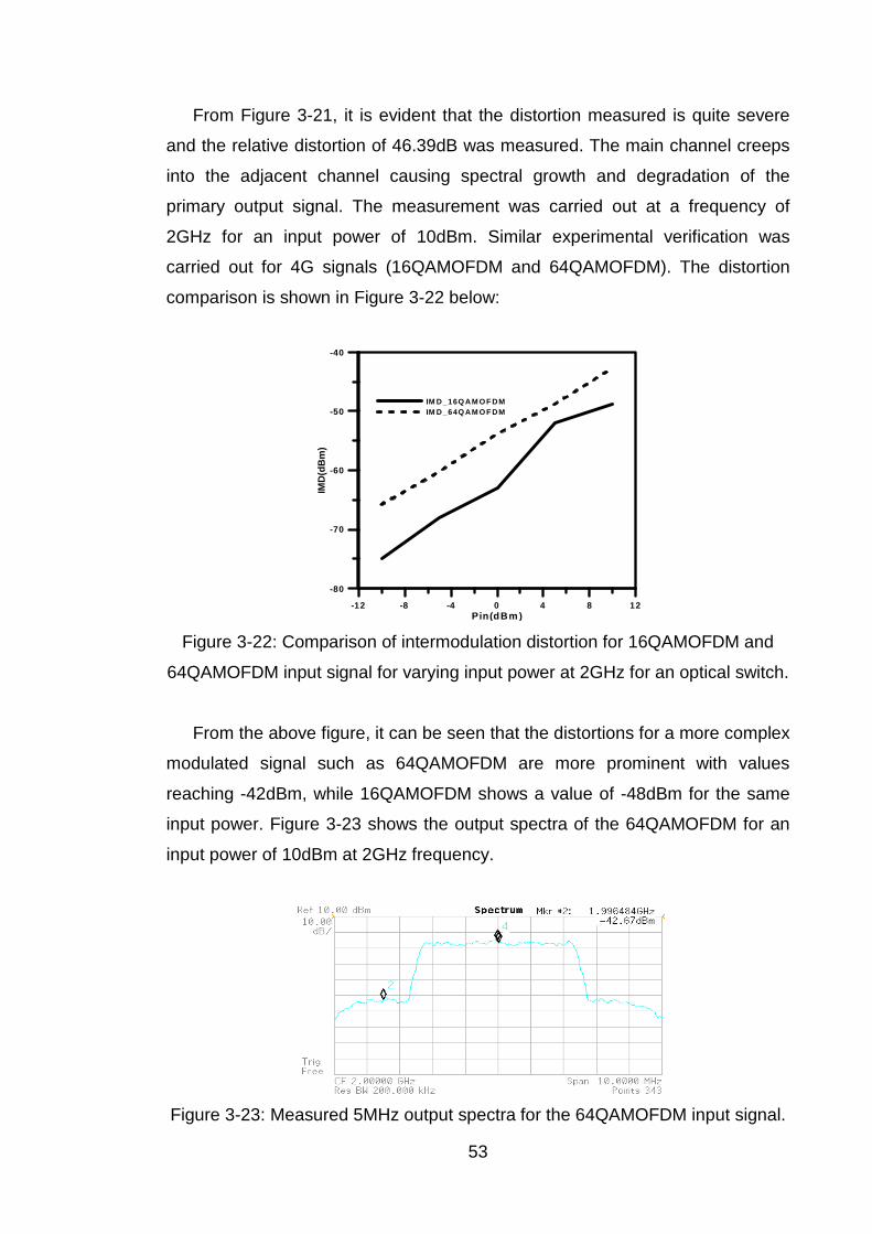
53
From Figure 3-21, it is evident that the distortion measured is quite severe
and the relative distortion of 46.39dB was measured. The main channel creeps
into the adjacent channel causing spectral growth and degradation of the
primary output signal. The measurement was carried out at a frequency of
2GHz for an input power of 10dBm. Similar experimental verification was
carried out for 4G signals (16QAMOFDM and 64QAMOFDM). The distortion
comparison is shown in Figure 3-22 below:
-12 -8 -4 0 4 8 12Pin(dBm )
-80
-70
-60
-50
-40
IMD
(dB
m)
IM D_16Q AM O F DMIM D_64Q AM O F DM
Figure 3-22: Comparison of intermodulation distortion for 16QAMOFDM and
64QAMOFDM input signal for varying input power at 2GHz for an optical switch.
From the above figure, it can be seen that the distortions for a more complex
modulated signal such as 64QAMOFDM are more prominent with values
reaching -42dBm, while 16QAMOFDM shows a value of -48dBm for the same
input power. Figure 3-23 shows the output spectra of the 64QAMOFDM for an
input power of 10dBm at 2GHz frequency.
Figure 3-23: Measured 5MHz output spectra for the 64QAMOFDM input signal.
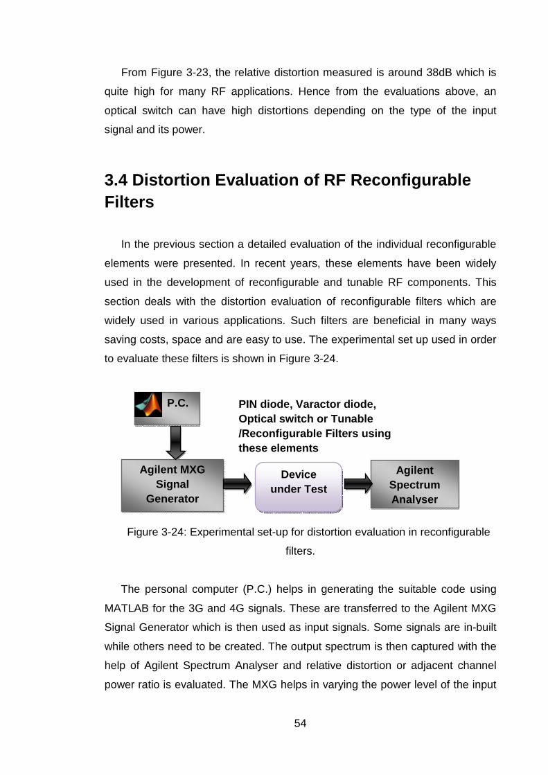
54
From Figure 3-23, the relative distortion measured is around 38dB which is
quite high for many RF applications. Hence from the evaluations above, an
optical switch can have high distortions depending on the type of the input
signal and its power.
3.4 Distortion Evaluation of RF Reconfigurable Filters
In the previous section a detailed evaluation of the individual reconfigurable
elements were presented. In recent years, these elements have been widely
used in the development of reconfigurable and tunable RF components. This
section deals with the distortion evaluation of reconfigurable filters which are
widely used in various applications. Such filters are beneficial in many ways
saving costs, space and are easy to use. The experimental set up used in order
to evaluate these filters is shown in Figure 3-24.
Figure 3-24: Experimental set-up for distortion evaluation in reconfigurable
filters.
The personal computer (P.C.) helps in generating the suitable code using
MATLAB for the 3G and 4G signals. These are transferred to the Agilent MXG
Signal Generator which is then used as input signals. Some signals are in-built
while others need to be created. The output spectrum is then captured with the
help of Agilent Spectrum Analyser and relative distortion or adjacent channel
power ratio is evaluated. The MXG helps in varying the power level of the input
P.C.
Agilent MXG Signal
Generator
Device under Test
Agilent Spectrum Analyser
PIN diode, Varactor diode, Optical switch or Tunable /Reconfigurable Filters using these elements

55
signal. Hence a comprehensive set of results are obtained to evaluate
distortions.
3.4.1 Filters using PIN diode as Reconfigurable Ele ment
Filters using PIN diode as reconfigurable elements are widely found in
literature. In [3.32] and [3.33], reconfigurable filters have been designed using
PIN diodes. Such filters help in switching from one response to another. For
example in [3.32], four PIN diodes are used in order to switch from a bandpass
to a bandstop response. Here a reconfigurable ultra wide band (UWB) filter was
chosen as DUT [3.34]. The filter is briefly described and then distortion results
are presented.
The structure of the filter is shown below in Figure 3-25. The filter works as a
bandpass filter in the ON state and as a bandstop filter in the OFF state. The
PIN diode (BAP65-02) is placed on a 0.3 mm gap. The filter operates within 3.1-
5GHz with the mid-band frequency at 4GHz.
Figure3-25: Photograph of the UWB reconfigurable filter (DUT).
The above filter is then evaluated for distortions using various input signals
with varying power level. A two tone set up was used where the signals were
placed 0.5MHz and 1MHz apart with centre frequency at 3.5GHz which falls in
the passband of the filter. For the first case where 0.5MHz was used to space
the two fundamental tones, it was found that the two fundamental frequencies
were at 3.49975GHz and 3.50025GHz. Hence the third order intermodulation
distortions will arise at 3.49925GHz and 3.50075GHz. For the second case, the
fundamental tones were at 3.4995GHz and 3.5005GHz while the third order

56
IMD occurs at 3.4985GHz and 3.5015GHz. Figure 3-26 shows the spectrum
captured in Agilent spectrum analyser. The IMD3 is prominently visible. The
input power of 15dBm was chosen to show the maximum effect of distortions.
(a) (b)
Figure 3-26: Spectrum showing the 3rd order intermodulation distortion for a
filter with PIN diode for Pin =15dBm (a) with 0.5MHz (b) with 1MHz spacing.
It is clear from the above figure that the distortions for 0.5MHz spaced
fundamental signals are more than the distortions for 1MHz spaced signals. A
similar result was found when the PIN diode was evaluated for distortions in the
previous section. Figure 3-27 shows the comparison of the third order IMD for
both cases along with the output power Pout when the input power Pin is varied.
-20 -10 0 10Pin(dBm)
-40
-30
-20
-10
0
Pou
t(dB
m)
-90
-80
-70
-60
-50
-40
IMD
3 (d
Bm
)
Pout_0.5Pout_1IMD3_0.5IMD3_1
Figure 3-27: Variation of Pout and IMD3 with respect to various input power Pin
for the reconfigurable filter using PIN diode.
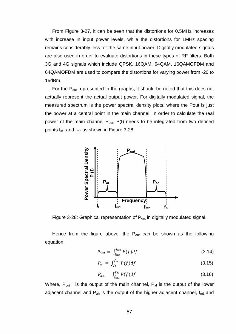
57
From Figure 3-27, it can be seen that the distortions for 0.5MHz increases
with increase in input power levels, while the distortions for 1MHz spacing
remains considerably less for the same input power. Digitally modulated signals
are also used in order to evaluate distortions in these types of RF filters. Both
3G and 4G signals which include QPSK, 16QAM, 64QAM, 16QAMOFDM and
64QAMOFDM are used to compare the distortions for varying power from -20 to
15dBm.
For the Pout represented in the graphs, it should be noted that this does not
actually represent the actual output power. For digitally modulated signal, the
measured spectrum is the power spectral density plots, where the Pout is just
the power at a central point in the main channel. In order to calculate the real
power of the main channel Pout, P(f) needs to be integrated from two defined
points fm1 and fm2 as shown in Figure 3-28.
Figure 3-28: Graphical representation of Pout in digitally modulated signal.
Hence from the figure above, the Pout can be shown as the following
equation.
.uv w .xgxt(tG (3.14)
.[y w .xgxtGz (3.15)
.[ w .xgx|t( (3.16)
Where, Pout is the output of the main channel, Pal is the output of the lower
adjacent channel and Pah is the output of the higher adjacent channel, fm1 and
f l fm1 fm2 fh
Pout
Pah Pal
Frequency Pow
er S
pect
ral D
ensi
ty
P (
f)
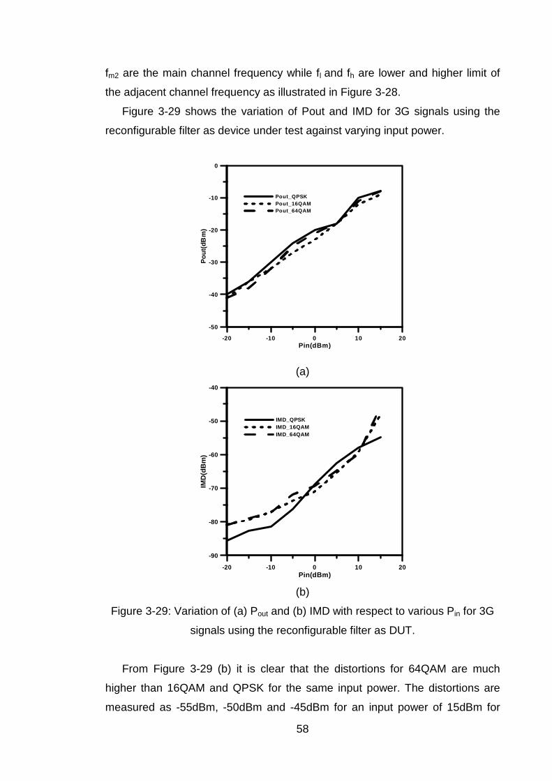
58
fm2 are the main channel frequency while fl and fh are lower and higher limit of
the adjacent channel frequency as illustrated in Figure 3-28.
Figure 3-29 shows the variation of Pout and IMD for 3G signals using the
reconfigurable filter as device under test against varying input power.
-20 -10 0 10 20Pin(dBm)
-50
-40
-30
-20
-10
0
Pou
t(dB
m)
Pout_QPSKPout_16QAMPout_64QAM
(a)
-20 -10 0 10 20Pin(dBm)
-90
-80
-70
-60
-50
-40
IMD
(dB
m)
IMD_QPSKIMD_16QAMIMD_64QAM
(b)
Figure 3-29: Variation of (a) Pout and (b) IMD with respect to various Pin for 3G
signals using the reconfigurable filter as DUT.
From Figure 3-29 (b) it is clear that the distortions for 64QAM are much
higher than 16QAM and QPSK for the same input power. The distortions are
measured as -55dBm, -50dBm and -45dBm for an input power of 15dBm for
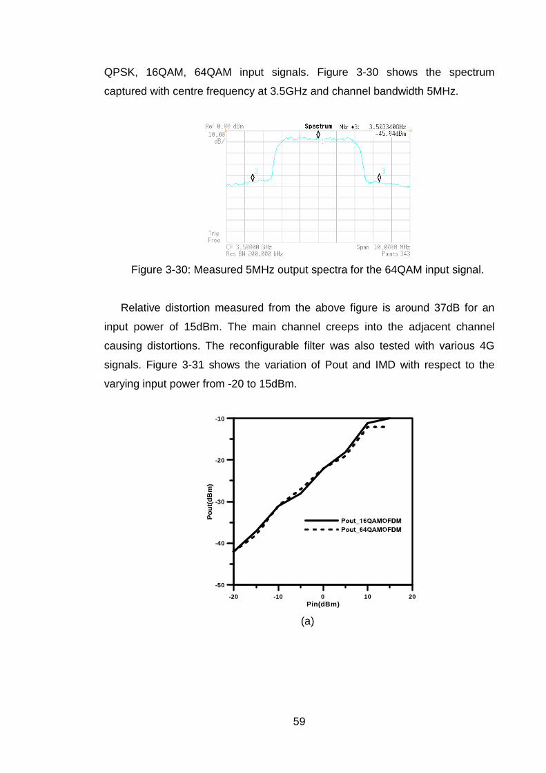
59
QPSK, 16QAM, 64QAM input signals. Figure 3-30 shows the spectrum
captured with centre frequency at 3.5GHz and channel bandwidth 5MHz.
Figure 3-30: Measured 5MHz output spectra for the 64QAM input signal.
Relative distortion measured from the above figure is around 37dB for an
input power of 15dBm. The main channel creeps into the adjacent channel
causing distortions. The reconfigurable filter was also tested with various 4G
signals. Figure 3-31 shows the variation of Pout and IMD with respect to the
varying input power from -20 to 15dBm.
-20 -10 0 10 20
Pin(dBm)
-50
-40
-30
-20
-10
Pou
t(dB
m)
(a)
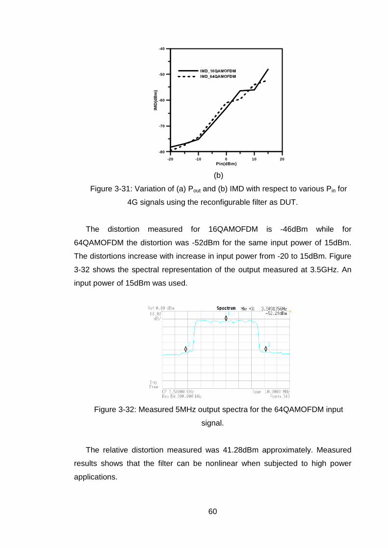
60
-20 -10 0 10 20Pin(dBm)
-80
-70
-60
-50
-40
IMD
(dB
m)
(b)
Figure 3-31: Variation of (a) Pout and (b) IMD with respect to various Pin for
4G signals using the reconfigurable filter as DUT.
The distortion measured for 16QAMOFDM is -46dBm while for
64QAMOFDM the distortion was -52dBm for the same input power of 15dBm.
The distortions increase with increase in input power from -20 to 15dBm. Figure
3-32 shows the spectral representation of the output measured at 3.5GHz. An
input power of 15dBm was used.
Figure 3-32: Measured 5MHz output spectra for the 64QAMOFDM input
signal.
The relative distortion measured was 41.28dBm approximately. Measured
results shows that the filter can be nonlinear when subjected to high power
applications.
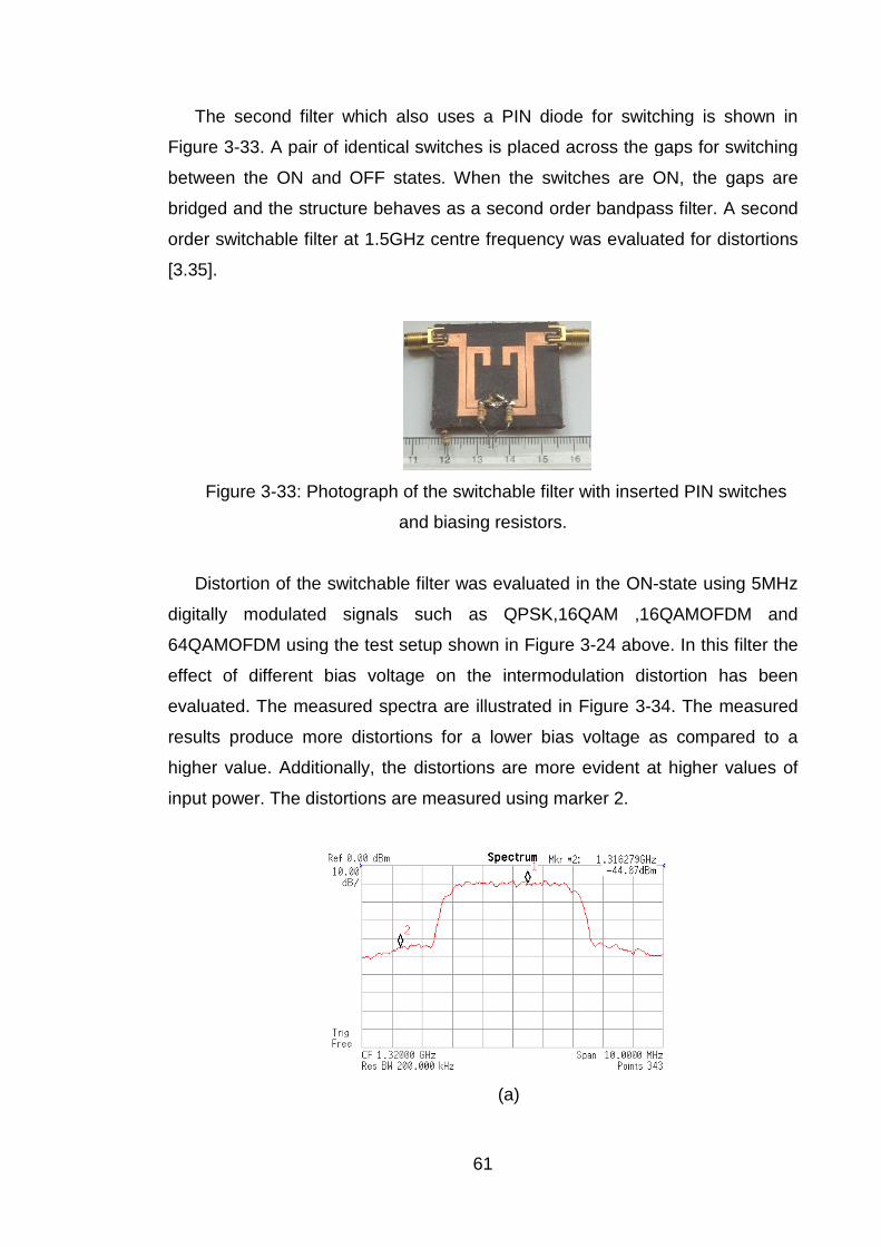
The second filter which also uses a
Figure 3-33. A pair of identical switches
between the ON and OFF states. When the switches are ON, the gaps are
bridged and the structure behave
order switchable filter at 1.5
[3.35].
Figure 3-33: Photograph of the s
Distortion of the
digitally modulated signals
64QAMOFDM using th
effect of different bias voltage on the intermodulation
evaluated. The measured spectr
results produce more distortions
higher value. Additionally, the distortions are more evident at higher values of
input power. The distortions are measured using marker 2.
61
The second filter which also uses a PIN diode for switching is shown in
A pair of identical switches is placed across the gaps for switching
between the ON and OFF states. When the switches are ON, the gaps are
bridged and the structure behaves as a second order bandpass filter. A sec
order switchable filter at 1.5GHz centre frequency was evaluate
Photograph of the switchable filter with inserted
and biasing resistors.
Distortion of the switchable filter was evaluated in the ON
digitally modulated signals such as QPSK,16QAM ,16QAMOFDM and
using the test setup shown in Figure 3-24 above
effect of different bias voltage on the intermodulation distortion has been
The measured spectra are illustrated in Figure 3
results produce more distortions for a lower bias voltage as compared to a
higher value. Additionally, the distortions are more evident at higher values of
ut power. The distortions are measured using marker 2.
(a)
witching is shown in
placed across the gaps for switching
between the ON and OFF states. When the switches are ON, the gaps are
s as a second order bandpass filter. A second
evaluated for distortions
witchable filter with inserted PIN switches
switchable filter was evaluated in the ON-state using 5MHz
such as QPSK,16QAM ,16QAMOFDM and
above. In this filter the
distortion has been
a are illustrated in Figure 3-34. The measured
for a lower bias voltage as compared to a
higher value. Additionally, the distortions are more evident at higher values of
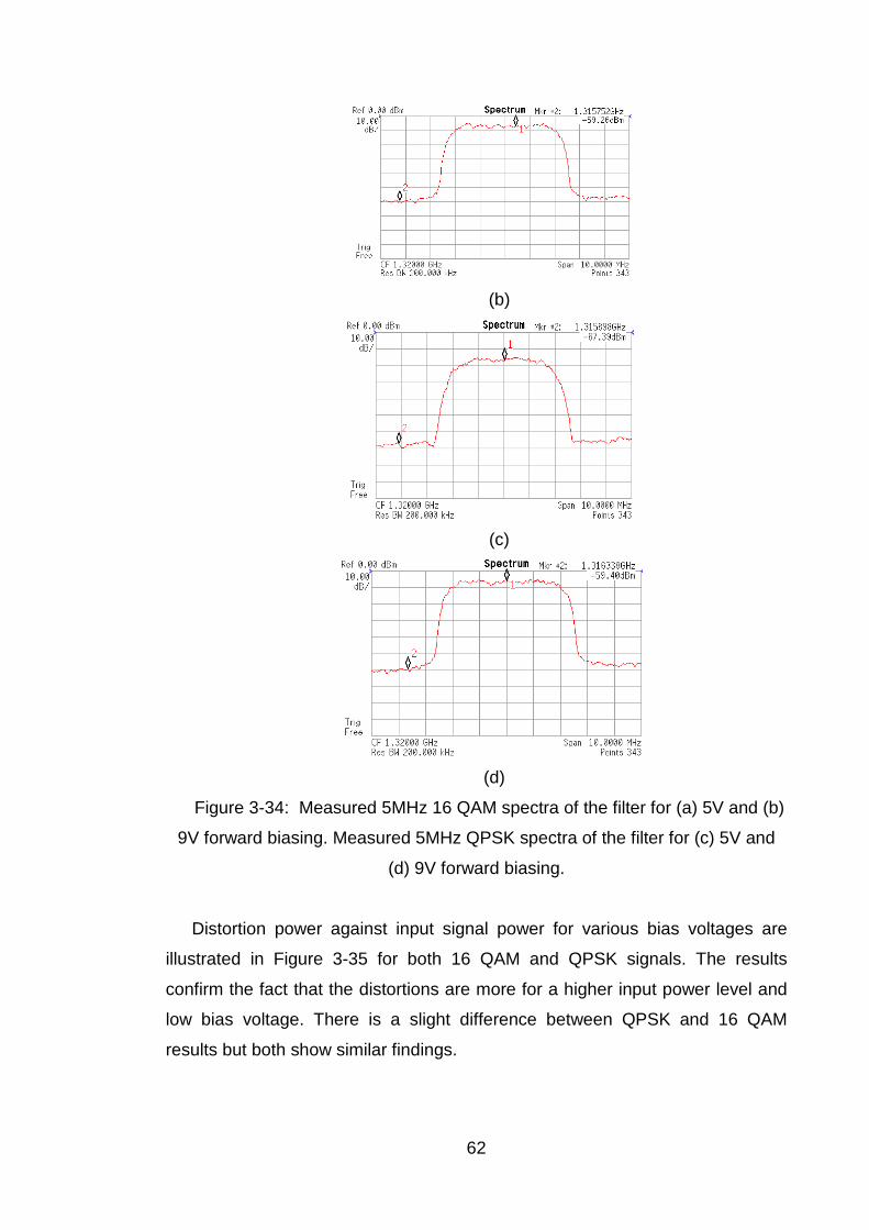
62
(b)
(c)
(d)
Figure 3-34: Measured 5MHz 16 QAM spectra of the filter for (a) 5V and (b)
9V forward biasing. Measured 5MHz QPSK spectra of the filter for (c) 5V and
(d) 9V forward biasing.
Distortion power against input signal power for various bias voltages are
illustrated in Figure 3-35 for both 16 QAM and QPSK signals. The results
confirm the fact that the distortions are more for a higher input power level and
low bias voltage. There is a slight difference between QPSK and 16 QAM
results but both show similar findings.
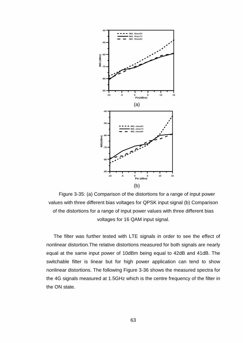
63
-10 -5 0 5 10 15Pin(dBm)
-90
-80
-70
-60
-50
-40
IMD
(dB
m)
IMD_Vbias5VIMD_Vbias7VIMD_Vbias9V
(a)
-10 -5 0 5 10 15Pin (dBm)
-90
-80
-70
-60
-50
-40
IMD
(dB
m)
IMD_vbias5VIMD_vbias7VIMD_vbias9V
(b)
Figure 3-35: (a) Comparison of the distortions for a range of input power
values with three different bias voltages for QPSK input signal (b) Comparison
of the distortions for a range of input power values with three different bias
voltages for 16 QAM input signal.
The filter was further tested with LTE signals in order to see the effect of
nonlinear distortion.The relative distortions measured for both signals are nearly
equal at the same input power of 10dBm being equal to 42dB and 41dB. The
switchable filter is linear but for high power application can tend to show
nonlinear distortions. The following Figure 3-36 shows the measured spectra for
the 4G signals measured at 1.5GHz which is the centre frequency of the filter in
the ON state.
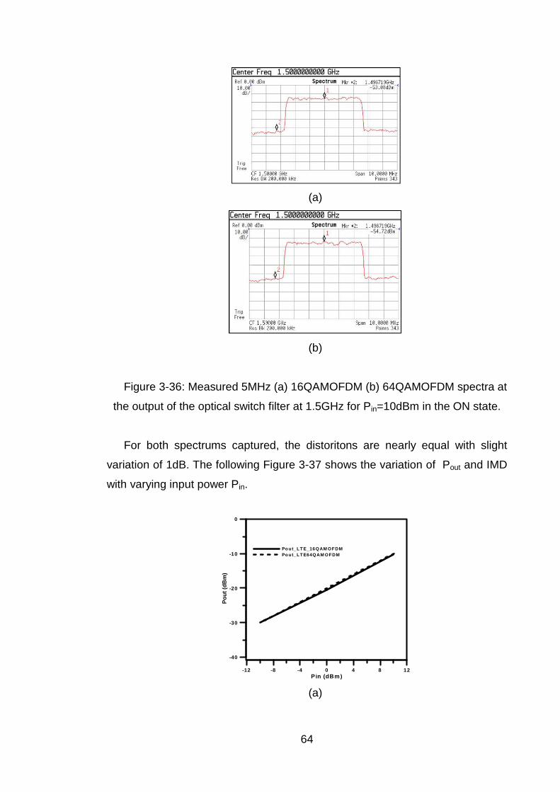
64
(a)
(b)
Figure 3-36: Measured 5MHz (a) 16QAMOFDM (b) 64QAMOFDM spectra at
the output of the optical switch filter at 1.5GHz for Pin=10dBm in the ON state.
For both spectrums captured, the distoritons are nearly equal with slight
variation of 1dB. The following Figure 3-37 shows the variation of Pout and IMD
with varying input power Pin.
-12 -8 -4 0 4 8 12Pin (dBm)
-40
-30
-20
-10
0
Pou
t (dB
m)
Po ut_LT E_16QAM OFDMPo ut_LT E64QAM OFDM
(a)

65
-12 -8 -4 0 4 8 12Pin(dBm)
-68
-64
-60
-56
-52
-48
-44
IMD
(dB
m)
IMD_LTE_16QAMOFDMIMD_LTE64QAMOFDM
(b)
Figure 3-37: Comparing the (a) output power spectrum and (b) distortion
power spectrum against the input power for 4G digitally modulated signals.
The above figure shows the output spectrum using 4G 16QAM and 64QAM
OFDM respectively as input signals. The output clearly has certain amount of
distortions. The IMD has been plotted against the input power and it is clearly
seen that the distortions increases for higher power levels. The plot for the
output power spectrum is linear indicating that the filter is also linear in nature.
Nonlinear distortion evaluation of a dual-mode PIN switched microstrip
bandpass filter was presented. As expected, the linearity of the filter suffers
more at higher input powers.
3.4.2 Filters using Optical Switch as Reconfigurabl e
Element
This section deals with the evaluation of distortion of RF filters using optical
switch as the switching element. For this purpose a reconfigurable UWB
bandpass filter, is taken and distortions evaluated. The filter layout is shown in
Figure 3-38 which has a 3dB passband from 3.1GHz – 5.0GHz with a mid-band
frequency of 4GHz [3-34] & [3-36].
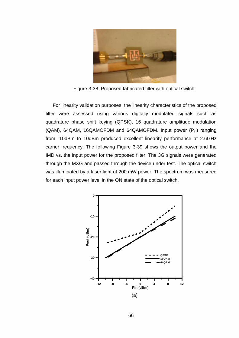
66
Figure 3-38: Proposed fabricated filter with optical switch.
For linearity validation purposes, the linearity characteristics of the proposed
filter were assessed using various digitally modulated signals such as
quadrature phase shift keying (QPSK), 16 quadrature amplitude modulation
(QAM), 64QAM, 16QAMOFDM and 64QAMOFDM. Input power (Pin) ranging
from -10dBm to 10dBm produced excellent linearity performance at 2.6GHz
carrier frequency. The following Figure 3-39 shows the output power and the
IMD vs. the input power for the proposed filter. The 3G signals were generated
through the MXG and passed through the device under test. The optical switch
was illuminated by a laser light of 200 mW power. The spectrum was measured
for each input power level in the ON state of the optical switch.
-12 -8 -4 0 4 8 12Pin (dBm)
-40
-30
-20
-10
0
Po
ut
(dB
m)
QPSK16QAM64QAM
(a)

67
-12 -8 -4 0 4 8 12Pin(dBm)
-72
-68
-64
-60
-56
IMD
(dB
m)
QPSK16QAM64QAM
(b)
Figure 3-39: Measured response for (a) output power Pout (b) IMD vs. Pin for
different digitally modulated signals (3G) for 2.6GHz carrier in the ON state of
the optical switch.
The distortions occur near the junction of the main channel and the adjacent
channel as shown in Figure 3-40. Using the spectrum, the relative distortion for
each can be calculated. The figure shows the output spectrum at 2.6GHz for an
input power of 10dBm.
(a)
(b)
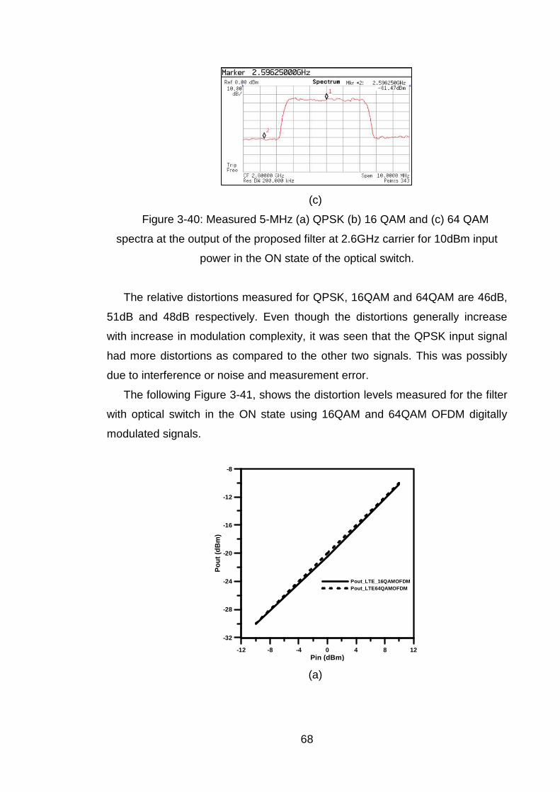
68
(c)
Figure 3-40: Measured 5-MHz (a) QPSK (b) 16 QAM and (c) 64 QAM
spectra at the output of the proposed filter at 2.6GHz carrier for 10dBm input
power in the ON state of the optical switch.
The relative distortions measured for QPSK, 16QAM and 64QAM are 46dB,
51dB and 48dB respectively. Even though the distortions generally increase
with increase in modulation complexity, it was seen that the QPSK input signal
had more distortions as compared to the other two signals. This was possibly
due to interference or noise and measurement error.
The following Figure 3-41, shows the distortion levels measured for the filter
with optical switch in the ON state using 16QAM and 64QAM OFDM digitally
modulated signals.
-12 -8 -4 0 4 8 12Pin (dBm)
-32
-28
-24
-20
-16
-12
-8
Po
ut
(dB
m)
Pout_LTE_16QAMOFDMPout_LTE64QAMOFDM
(a)
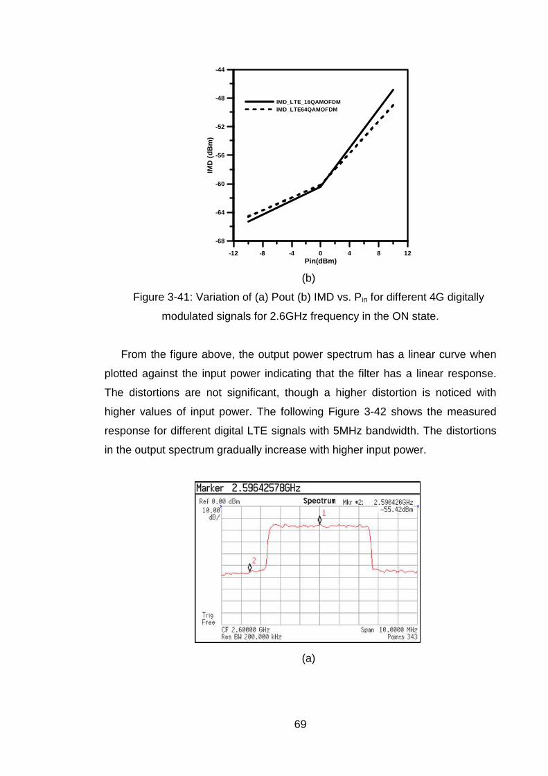
69
-12 -8 -4 0 4 8 12Pin(dBm)
-68
-64
-60
-56
-52
-48
-44
IMD
(d
Bm
)
IMD_LTE_16QAMOFDMIMD_LTE64QAMOFDM
(b)
Figure 3-41: Variation of (a) Pout (b) IMD vs. Pin for different 4G digitally
modulated signals for 2.6GHz frequency in the ON state.
From the figure above, the output power spectrum has a linear curve when
plotted against the input power indicating that the filter has a linear response.
The distortions are not significant, though a higher distortion is noticed with
higher values of input power. The following Figure 3-42 shows the measured
response for different digital LTE signals with 5MHz bandwidth. The distortions
in the output spectrum gradually increase with higher input power.
(a)
70
(b)
Figure 3-42: Measured 5-MHz spectra at the output of the optical switch
filter at 2.6GHz for (a) 16QAMOFDM and (b) 64QAMOFDM for 10dBm input
power for different 4G input signals for the ON state.
Figure 3-42 shows that the increase of nonlinear distortions with input
power. The upper adjacent channel power ratio (ACPR) is also measured and
tabulated in Table 3-2 & 3-3 for both 16QAM and 64QAM OFDM input signals
respectively. Marker 1 represents the average power level of the main channel
(Pout) while Marker 2 represents the average power level of the lower adjacent
channel (IMD). The output spectra for the higher input power level of 10dbm are
presented. This is a measure of the relative distortion in the lower channel or
the difference between the main channel average power level and the lower
adjacent channel average power level. Due to the effects of nonlinearity, the
signal in the adjacent channel sometimes interferes with the main channel
signal. This leads to spectral regrowth. Hence relative distortion gives a good
measure for digitally modulated signals. Higher the relative distortion more is
the linearity of the DUT.
PIN
(dBm)
POUT
(dBm)
IMD
(dBm)
ACPR
(dB)
-10 -30 -70.6 40.6
0 -20.5 -60.4 39.9
10 -10.2 -46.8 36.6
Table 3-2: Measured data for distortion evaluation using 16QAMOFDM.
71
PIN
(dBm)
POUT
(dBm)
IMD
(dBm)
ACPR
(dB)
-10 -30 -71.2 41.2
0 -20 -60.17 40.17
10 -10 -49.02 39.02
Table 3-3: Measured data for distortion evaluation using 64QAMOFDM.
Table 3-2 & 3-3 shows the tabulated measured value of the output spectrum
for 16QAM OFDM and 64QAM OFDM input signal respectively. By comparing
the relative distortion or ACPR we can see that with higher power levels,
distortion increases. Overall the filter is highly linear and can be used in most
applications.
3.5 Conclusion
This chapter introduced the main concepts of nonlinear distortions including
numerical analysis of third order intermodulation distortion, power series
analysis and using two tone tests for distortion measurements. The various
elements used in RF reconfigurable/tunable circuits such as PIN diodes,
varactor diodes and optical switches were introduced. A comprehensive set of
simulations to establish the amount of distortion were presented for all three
components.
Further experimental verification was made for PIN diodes and optical
switches using various input signals with power varying from -20dBm to 15dBm.
The results were thoroughly discussed and a set of comparison was given
among various other tunable/switchable elements such as RF MEMS, liquid
crystal etc. Few reconfigurable filters using PIN switch and optical switch were
further evaluated for distortions. A variation of input power, bias voltage, 3G and
4G signals have been used to measure and evaluate distortions to get a
complete picture. Measuring the nonlinear distortion of these components helps
in quantifying the amount of nonlinear distortion contribution made by such
elements in a transceiver system when interfering signals form additional
distortion products in the final output.

72
3.6 References [3.1] Q.Gu, RF System Design of Transceivers for Wireless Communications,
Springer, 2005, ISBN: 978-0-387-24161-6.
[3.2] S. Maas, Nonlinear Microwave and RF Circuits, Artech House Publishers,
2003, ISBN 1580534848.
[3.3] D. Pozar, Microwave Engineering, 3rd edition, John Wiley & Sons, 2004,
ISBN0471170968.
[3.4] J. C. Pedro, and N. B. De Carvalho, "On the use of multi-tone techniques
for assessing RF components' intermodulation distortion," IEEE Transactions
on Microwave Theory and Techniques, vol. 47, no. 12, pp. 2393-2402, Dec.
1999.
[3.5] J. Vuolevi, T. Rahkonen, Distortion in RF Power Amplifiers, Artech House
Inc., 2003, ISBN 1580535399.
[3.6] G. Collins, and D. W. Runton, "Nonlinear analysis of power amplifiers,"
Microwave Journal, vol. 50, no. 9, p. 164, Sept. 2007.
[3.7] B. Carey-Smith, and P. Warr, “Distortion Mechanisms in Varactor Diode-
Tuned Microwave Filters”, IEEE Transactions on Microwave Theory and
Techniques, Vol-54, No-9, Sept 2006, pp. 3492-3500.
[3.8] B. Doherty, “PIN Diode Fundamentals”, Microsemi Watertown, MicroNote
Series 701, available from < http://www.microsemi.com/micnotes/701.pdf>
accessed on 14th January, 2011.
[3.9] R.Caverly and G. Hiller, “Distortion Properties of MESFET and PIN Diode
Microwave Switches” IEEE MTT-S Digest, 1992, pp. 533-536.
[3.10] R.Caverly and G. Hiller, “Distortion in p-i-n Diode Control Circuits” IEEE
Transactions on Microwave Theory and Techniques, Vol.MTT-35,No-5,May
1987, pp.492-501.
[3.11] BAP65-02 Product Data Sheet, NXP Semiconductors, January 2008.
[3.12] K.Rabbi, L. Athukorala, C.J. Panagamuwa, J.C. Vardaxoglou, D.Budimir,
“High-Linearity Reconfigurable Microstrip UWB Bandpass Filters” IEEE
Microwave and Wireless Components Letters, Oct 2010.
[3.13] M. Watertown, “The PIN diode circuit designers’ handbook,” Microsemi
Corporation, Santa-Ana, CA, Jul. 1992.
73
[3.14] V. Cojocaru and F. Sischka, "Non-linear modelling of microwave PIN
diode switches for harmonic and intermodulation distortion simulation,"
Microwave Symposium Digest, 2003 IEEE MTT-S International , vol.2, no.,
pp.655,658 vol.2, 8-13 June 2003.
[3.15] B. Carey-Smith, and P. Warr, “Distortion Mechanisms in Varactor Diode-
Tuned Microwave Filters”, IEEE Transactions on Microwave Theory and
Techniques, Vol-54, No-9, Sept 2006, pp. 3492-3500.
[3.16] V. Sekar and K. Entesari, “ Nonlinear Nodal Analysis of Varactor-tuned
Microwave Filters” ,Proceedings of the 40th European Microwave Conference ,
Paris, Sept 2010, pp. 1241-1244
[3.17]Skyworks Solutions “Varactor Diodes”, available from
<http://www.skyworksinc.com/uploads/documents/200824a.pdf> accessed on
20th September, 2012.
[3.18] V. Sekar and K. Entesari, “ Nonlinear Nodal Analysis of Varactor-tuned
Microwave Filters” ,Proceedings of the 40th European Microwave Conference ,
Paris, Sept 2010, pp. 1241-1244.
[3.19] K.Buisman, L.C.N. de Vreede, L.K. Nanver, ““Distortion-Free” Varactor
Diode Topologies for RF Adaptivity” IEEE, 2005, pp.157-160.
[3.20] K.Buisman, C.Huang, A.Akhnoukh, L.K.Nanver,”Varactor Topologies for
RF Adaptivity with Improved Power Handling and Linearity”, IEEE, 2007, pp-
319-322.
[3.21] C. H. Lee, P. S. Mak, and A. P. DeFonzo, “Optical control of millimetre
wave propagation in dielectric waveguides,” IEEE J. Quantum Electron., vol. 16,
no. 3, pp. 277–288, 1980
[3.22] D. Draskovic and D. Budimir, “Optically controlled negative refractive
index transmission lines”, European Conference on Antennas and Propagation,
pp. 1672-1674, 2009.
[3.23] C.J. Panagamuwa, A. Chauraya and J.Y.C Vardaxoglu, “Frequency and
beam reconfigurable antenna using photoconducting switches”, IEEE
Transactions of Antennas and Propagation, vol. 54, No. 2, pp. 449 -454, 2006.
[3.24] G. Zouganelis and D. Budimir, “Silicon gap-loaded microstrip slit-
tetragonal resonator under IR-radiation”, Microwave and Optical Technology
Letters, vol. 49, pp. 699-702, 2007.
74
[3.25] D. Draskovic and D. Budimir, “Optically reconfigurable dual-band
compact branch-line couplers”, European Conference on Antennas and
Propagation, pp. 1-3, 2007.
[3.26] G.M.Loubriel, F.J. Zutavern, A.G. Baca, H.P. Hjalmarson, T.A. Plut, W.D.
Helgeson, M.W. O'Malley, M.H. Ruebush and D.J. Brown, "Photoconductive
semiconductor switches," Plasma Science, IEEE Transactions on , vol.25, no.2,
pp.124,130, Apr 1997.
[3.27] A. Karabegovic, M. Robert O’Connell and W.C. Nunnally,
"Photoconductive Semiconductor Switch for Microwave Applications," IEEE
International Power Modulators and High Voltage Conference, Proceedings of
the 2008, vol., no., pp.9, 12, 27-31 May 2008.
[3.28] T. Bouchemat, F. Hobar, A. Koster, S. Laval, M. Bouchemat, and D.
Pascal. "Theoretical study of a nonlinear fast silicon photoconductive
switch." The European Physical Journal Applied Physics 6, no. 02, 1999, pp:
165-169.
[3.29] G.M.Loubriel, et al., “Longevity of optically activated, high gain GaAs
photoconductive semiconductor switches”, IEEE Transactions on Plasma
Science, vol. 26, no. 5, October 1998, pp1393–1402.
[3.30]Federal Communication Commission, “Revision of part 15 of the
Commission’s rules regarding ultra-wideband transmission systems”,
<http://transition.fcc.gov/Bureaus/Engineering_Technology/Orders/2002/fcc020
48.pdf > Accessed on 19th Aug 2014.
[3.31] National Telecommunication and Information Administration, “Spectrum
Sharing Innovation Test-bed Pilot Program Phase 1 Test Plan”, February 2009,
<http://www.ntia.doc.gov/files/ntia/publications/phase_i_test_plan_final_021220
09.pdf> Accessed on 20th Aug 2014.
[3.32] M.F. Karim, Y.X Guo, Z.N. Chan and L.C. Ong, “Miniaturized
reconfigurable and switchable filter from UWB to 2.4 Hz LAN using PIN diodes”,
IEEE MTT-S, pp. 509-512, 2009.
[3.33]Y.H. Chun, H. Shamman, J.S. Hong, “Switchable embedded notch
structure for UWB bandpass filter”, IEEE Microwave and Wireless Component
Letters, vol. 18, no. 9, pp. 590 –592, 2008.
[3.34] K. Rabbi, L. Athukorala, C.J. Panagamuwa, J.C. Vardaxoglou, D.
Budimir, "High-linearity reconfigurable microstrip UWB bandpass filters,"

75
Microwave Integrated Circuits Conference (EuMIC), 2011 European , vol., no.,
pp.172,175, 10-11 Oct. 2011.
[3.36] K. Chakrabarty, L. Athukorala and D. Budimir, "High linearity switchable
dual-mode microstrip bandpass filters," Microwave Conference Proceedings
(APMC), 2011 Asia-Pacific , vol., no., pp.1019,1022, 5-8 Dec. 2011.
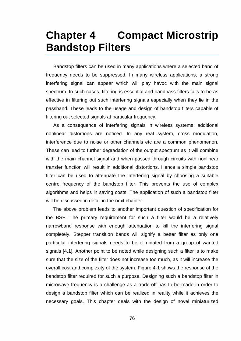
76
Chapter 4 Compact Microstrip Bandstop Filters
Bandstop filters can be used in many applications where a selected band of
frequency needs to be suppressed. In many wireless applications, a strong
interfering signal can appear which will play havoc with the main signal
spectrum. In such cases, filtering is essential and bandpass filters fails to be as
effective in filtering out such interfering signals especially when they lie in the
passband. These leads to the usage and design of bandstop filters capable of
filtering out selected signals at particular frequency.
As a consequence of interfering signals in wireless systems, additional
nonlinear distortions are noticed. In any real system, cross modulation,
interference due to noise or other channels etc are a common phenomenon.
These can lead to further degradation of the output spectrum as it will combine
with the main channel signal and when passed through circuits with nonlinear
transfer function will result in additional distortions. Hence a simple bandstop
filter can be used to attenuate the interfering signal by choosing a suitable
centre frequency of the bandstop filter. This prevents the use of complex
algorithms and helps in saving costs. The application of such a bandstop filter
will be discussed in detail in the next chapter.
The above problem leads to another important question of specification for
the BSF. The primary requirement for such a filter would be a relatively
narrowband response with enough attenuation to kill the interfering signal
completely. Stepper transition bands will signify a better filter as only one
particular interfering signals needs to be eliminated from a group of wanted
signals [4.1]. Another point to be noted while designing such a filter is to make
sure that the size of the filter does not increase too much, as it will increase the
overall cost and complexity of the system. Figure 4-1 shows the response of the
bandstop filter required for such a purpose. Designing such a bandstop filter in
microwave frequency is a challenge as a trade-off has to be made in order to
design a bandstop filter which can be realized in reality while it achieves the
necessary goals. This chapter deals with the design of novel miniaturized
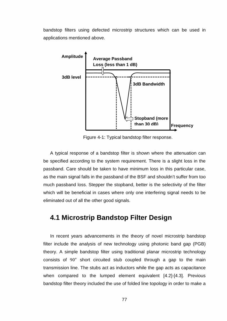
77
bandstop filters using defected microstrip structures which can be used in
applications mentioned above.
Figure 4-1: Typical bandstop filter response.
A typical response of a bandstop filter is shown where the attenuation can
be specified according to the system requirement. There is a slight loss in the
passband. Care should be taken to have minimum loss in this particular case,
as the main signal falls in the passband of the BSF and shouldn’t suffer from too
much passband loss. Stepper the stopband, better is the selectivity of the filter
which will be beneficial in cases where only one interfering signal needs to be
eliminated out of all the other good signals.
4.1 Microstrip Bandstop Filter Design
In recent years advancements in the theory of novel microstrip bandstop
filter include the analysis of new technology using photonic band gap (PGB)
theory. A simple bandstop filter using traditional planar microstrip technology
consists of 90° short circuited stub coupled through a gap to the main
transmission line. The stubs act as inductors while the gap acts as capacitance
when compared to the lumped element equivalent [4.2]-[4.3]. Previous
bandstop filter theory included the use of folded line topology in order to make a
3dB level
Amplitude
Frequency
Average Passband Loss (less than 1 dB)
3dB Bandwidth
Stopband (more than 30 dB)
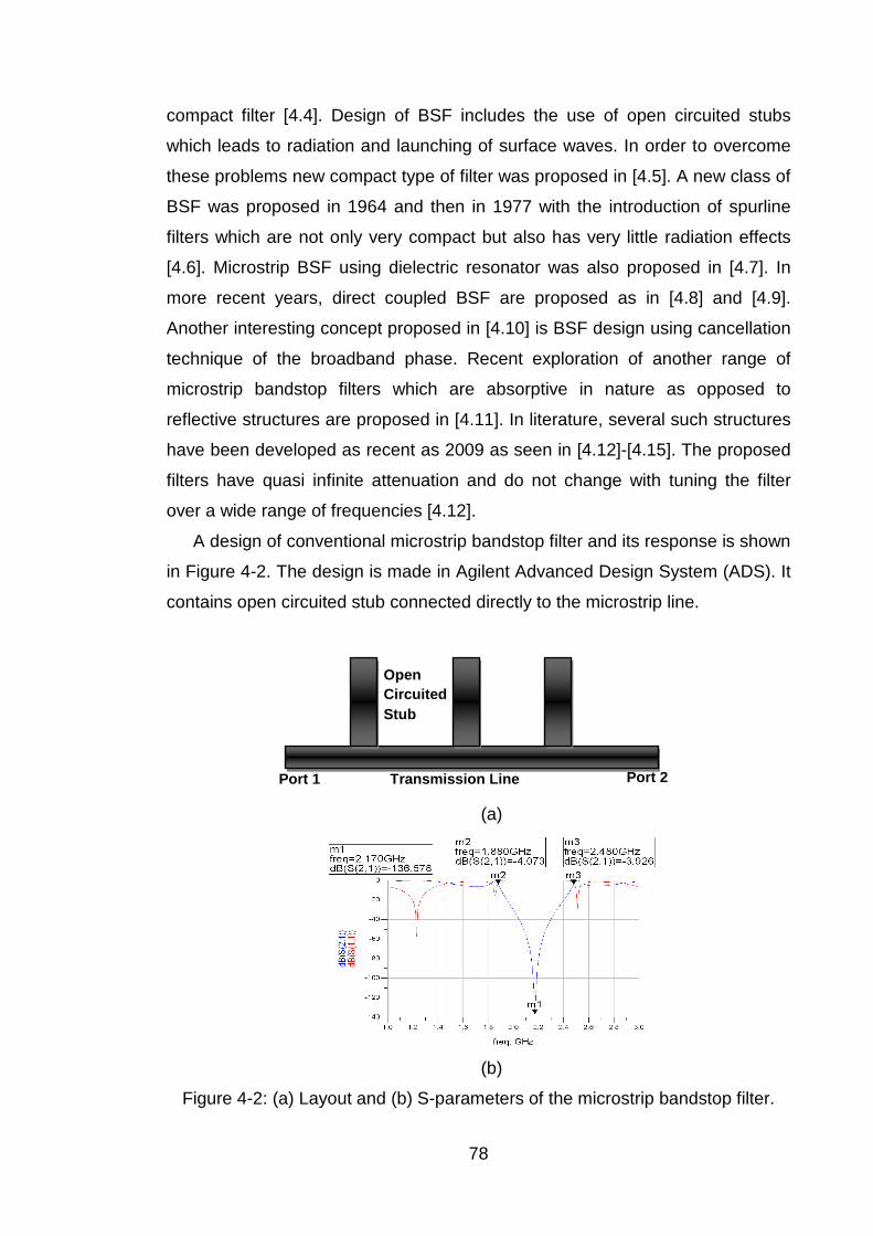
78
compact filter [4.4]. Design of BSF includes the use of open circuited stubs
which leads to radiation and launching of surface waves. In order to overcome
these problems new compact type of filter was proposed in [4.5]. A new class of
BSF was proposed in 1964 and then in 1977 with the introduction of spurline
filters which are not only very compact but also has very little radiation effects
[4.6]. Microstrip BSF using dielectric resonator was also proposed in [4.7]. In
more recent years, direct coupled BSF are proposed as in [4.8] and [4.9].
Another interesting concept proposed in [4.10] is BSF design using cancellation
technique of the broadband phase. Recent exploration of another range of
microstrip bandstop filters which are absorptive in nature as opposed to
reflective structures are proposed in [4.11]. In literature, several such structures
have been developed as recent as 2009 as seen in [4.12]-[4.15]. The proposed
filters have quasi infinite attenuation and do not change with tuning the filter
over a wide range of frequencies [4.12].
A design of conventional microstrip bandstop filter and its response is shown
in Figure 4-2. The design is made in Agilent Advanced Design System (ADS). It
contains open circuited stub connected directly to the microstrip line.
(a)
(b)
Figure 4-2: (a) Layout and (b) S-parameters of the microstrip bandstop filter.
Open Circuited Stub
Transmission Line Port 1 Port 2
79
The above structure has been designed in ADS using transmission lines and
quarter wavelength resonators. The transmission zeroes for the above circuit is
created at 2.18GHz. The S-parameter response of the BSF shows an
attenuation of nearly 140dB. As can be seen from the above response, the filter
has a very good attenuation but while calculating the 3dB bandwidth of the BSF
from the markers m2 and m3 it was found to be 0.6GHz. While trying to
optimize the circuit further it was noticed that there is an inverse relationship to
the amount of attenuation that can be achieved and the bandwidth of the filter.
Hence a balance was created, but this structure can be further improvised to
get a narrower bandwidth but at the expense of attenuation in the stopband.
The downside of the structure is the increased size of the filter.
Another example of a coupled microstrip bandstop filter is shown in Figure
4-3. The design which is discussed here is that of a compact microstrip
bandstop filter and has a miniaturized structure with a narrower bandwidth, but
the attenuation of the filter, is reduced to around 16dB. The following Figure 4-3
shows the layout of the structure developed in EM Sonnet.
Figure 4-3: Layout of the proposed structure of the bandstop filter.
As can be seen, there is a strong coupling between the two transmission
lines as shown in the figure above. A hairpin structure has been implemented
with the u-shaped resonator folded in order to reduce space. The resonator is
strongly coupled to the main transmission line through a gap. The gap is
capacitive in nature. The variation of the coupling determines the response of
the filter. With a weaker coupling the stopband response is degraded. Figure 4-
4 shows the measured response of the fabricated filter.
Strong coupling
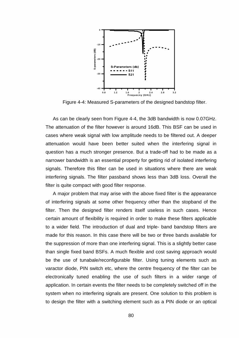
80
0 .8 1 .2 1 .6 2 2.4 2.8 3.2Freq uecny (G H z)
-40
-30
-20
-10
0
S-p
aram
ete
rs (
dB)
Figure 4-4: Measured S-parameters of the designed bandstop filter.
As can be clearly seen from Figure 4-4, the 3dB bandwidth is now 0.07GHz.
The attenuation of the filter however is around 16dB. This BSF can be used in
cases where weak signal with low amplitude needs to be filtered out. A deeper
attenuation would have been better suited when the interfering signal in
question has a much stronger presence. But a trade-off had to be made as a
narrower bandwidth is an essential property for getting rid of isolated interfering
signals. Therefore this filter can be used in situations where there are weak
interfering signals. The filter passband shows less than 3dB loss. Overall the
filter is quite compact with good filter response.
A major problem that may arise with the above fixed filter is the appearance
of interfering signals at some other frequency other than the stopband of the
filter. Then the designed filter renders itself useless in such cases. Hence
certain amount of flexibility is required in order to make these filters applicable
to a wider field. The introduction of dual and triple- band bandstop filters are
made for this reason. In this case there will be two or three bands available for
the suppression of more than one interfering signal. This is a slightly better case
than single fixed band BSFs. A much flexible and cost saving approach would
be the use of tunabale/reconfigurable filter. Using tuning elements such as
varactor diode, PIN switch etc, where the centre frequency of the filter can be
electronically tuned enabling the use of such filters in a wider range of
application. In certain events the filter needs to be completely switched off in the
system when no interfering signals are present. One solution to this problem is
to design the filter with a switching element such as a PIN diode or an optical
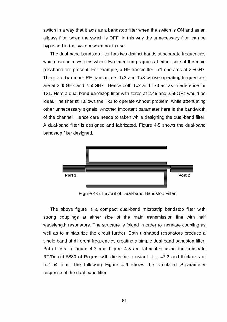
81
switch in a way that it acts as a bandstop filter when the switch is ON and as an
allpass filter when the switch is OFF. In this way the unnecessary filter can be
bypassed in the system when not in use.
The dual-band bandstop filter has two distinct bands at separate frequencies
which can help systems where two interfering signals at either side of the main
passband are present. For example, a RF transmitter Tx1 operates at 2.5GHz.
There are two more RF transmitters Tx2 and Tx3 whose operating frequencies
are at 2.45GHz and 2.55GHz. Hence both Tx2 and Tx3 act as interference for
Tx1. Here a dual-band bandstop filter with zeros at 2.45 and 2.55GHz would be
ideal. The filter still allows the Tx1 to operate without problem, while attenuating
other unnecessary signals. Another important parameter here is the bandwidth
of the channel. Hence care needs to taken while designing the dual-band filter.
A dual-band filter is designed and fabricated. Figure 4-5 shows the dual-band
bandstop filter designed.
Figure 4-5: Layout of Dual-band Bandstop Filter.
The above figure is a compact dual-band microstrip bandstop filter with
strong couplings at either side of the main transmission line with half
wavelength resonators. The structure is folded in order to increase coupling as
well as to miniaturize the circuit further. Both u-shaped resonators produce a
single-band at different frequencies creating a simple dual-band bandstop filter.
Both filters in Figure 4-3 and Figure 4-5 are fabricated using the substrate
RT/Duroid 5880 of Rogers with dielectric constant of εr =2.2 and thickness of
h=1.54 mm. The following Figure 4-6 shows the simulated S-parameter
response of the dual-band filter:
Port 1 Port 2
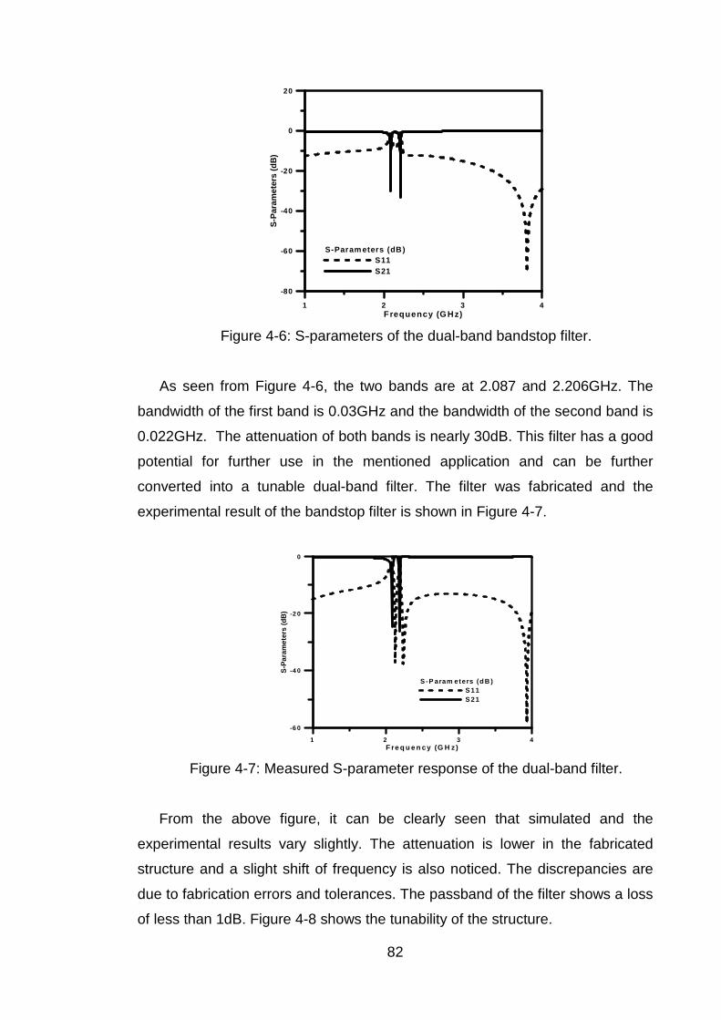
82
1 2 3 4Frequency (G Hz)
-80
-60
-40
-20
0
20
S-P
aram
eter
s (d
B)
S-Param eters (dB)S11S21
Figure 4-6: S-parameters of the dual-band bandstop filter.
As seen from Figure 4-6, the two bands are at 2.087 and 2.206GHz. The
bandwidth of the first band is 0.03GHz and the bandwidth of the second band is
0.022GHz. The attenuation of both bands is nearly 30dB. This filter has a good
potential for further use in the mentioned application and can be further
converted into a tunable dual-band filter. The filter was fabricated and the
experimental result of the bandstop filter is shown in Figure 4-7.
1 2 3 4F re q u e n c y (G H z)
-6 0
-4 0
-2 0
0
S-P
aram
eter
s (d
B)
S -P aram eters (d B )S 11S 21
Figure 4-7: Measured S-parameter response of the dual-band filter.
From the above figure, it can be clearly seen that simulated and the
experimental results vary slightly. The attenuation is lower in the fabricated
structure and a slight shift of frequency is also noticed. The discrepancies are
due to fabrication errors and tolerances. The passband of the filter shows a loss
of less than 1dB. Figure 4-8 shows the tunability of the structure.
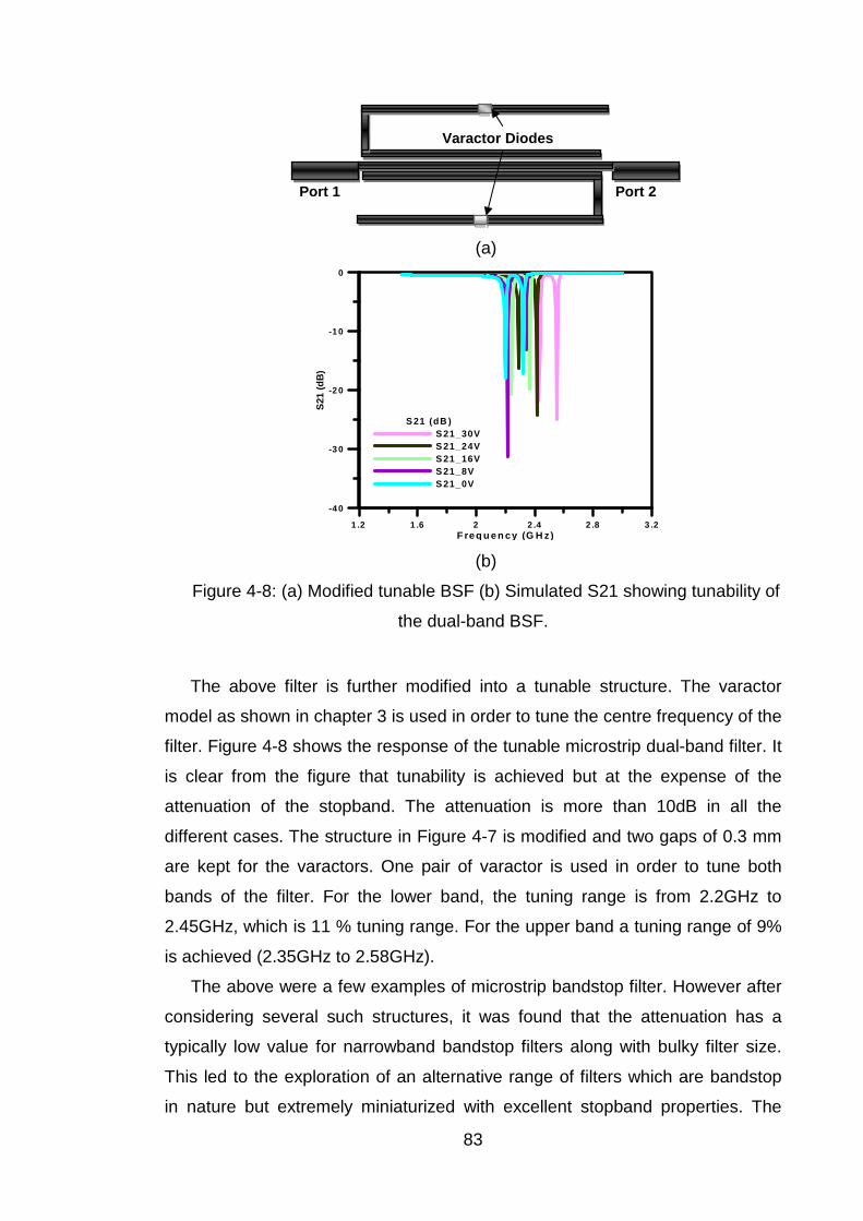
83
(a)
1 .2 1 .6 2 2 .4 2 .8 3 .2F req u en cy (G H z)
-4 0
-3 0
-2 0
-1 0
0
S21
(dB
)
S 21 (dB )S 21_30VS 21_24VS 21_16VS 21_8VS 21_0V
(b)
Figure 4-8: (a) Modified tunable BSF (b) Simulated S21 showing tunability of
the dual-band BSF.
The above filter is further modified into a tunable structure. The varactor
model as shown in chapter 3 is used in order to tune the centre frequency of the
filter. Figure 4-8 shows the response of the tunable microstrip dual-band filter. It
is clear from the figure that tunability is achieved but at the expense of the
attenuation of the stopband. The attenuation is more than 10dB in all the
different cases. The structure in Figure 4-7 is modified and two gaps of 0.3 mm
are kept for the varactors. One pair of varactor is used in order to tune both
bands of the filter. For the lower band, the tuning range is from 2.2GHz to
2.45GHz, which is 11 % tuning range. For the upper band a tuning range of 9%
is achieved (2.35GHz to 2.58GHz).
The above were a few examples of microstrip bandstop filter. However after
considering several such structures, it was found that the attenuation has a
typically low value for narrowband bandstop filters along with bulky filter size.
This led to the exploration of an alternative range of filters which are bandstop
in nature but extremely miniaturized with excellent stopband properties. The
Port 1 Port 2
Varactor Diodes
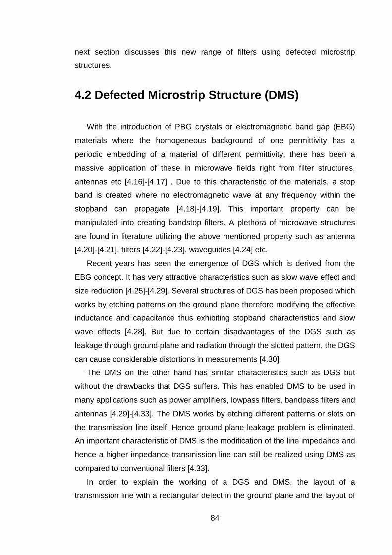
84
next section discusses this new range of filters using defected microstrip
structures.
4.2 Defected Microstrip Structure (DMS)
With the introduction of PBG crystals or electromagnetic band gap (EBG)
materials where the homogeneous background of one permittivity has a
periodic embedding of a material of different permittivity, there has been a
massive application of these in microwave fields right from filter structures,
antennas etc [4.16]-[4.17] . Due to this characteristic of the materials, a stop
band is created where no electromagnetic wave at any frequency within the
stopband can propagate [4.18]-[4.19]. This important property can be
manipulated into creating bandstop filters. A plethora of microwave structures
are found in literature utilizing the above mentioned property such as antenna
[4.20]-[4.21], filters [4.22]-[4.23], waveguides [4.24] etc.
Recent years has seen the emergence of DGS which is derived from the
EBG concept. It has very attractive characteristics such as slow wave effect and
size reduction [4.25]-[4.29]. Several structures of DGS has been proposed which
works by etching patterns on the ground plane therefore modifying the effective
inductance and capacitance thus exhibiting stopband characteristics and slow
wave effects [4.28]. But due to certain disadvantages of the DGS such as
leakage through ground plane and radiation through the slotted pattern, the DGS
can cause considerable distortions in measurements [4.30].
The DMS on the other hand has similar characteristics such as DGS but
without the drawbacks that DGS suffers. This has enabled DMS to be used in
many applications such as power amplifiers, lowpass filters, bandpass filters and
antennas [4.29]-[4.33]. The DMS works by etching different patterns or slots on
the transmission line itself. Hence ground plane leakage problem is eliminated.
An important characteristic of DMS is the modification of the line impedance and
hence a higher impedance transmission line can still be realized using DMS as
compared to conventional filters [4.33].
In order to explain the working of a DGS and DMS, the layout of a
transmission line with a rectangular defect in the ground plane and the layout of

85
a transmission line with a T-shaped defect on the line itself respectively are
shown. When the ground plane is defected, the current distribution changes
along with the change in the propagation properties. A similar case is seen in the
case of the DMS, where the current distribution is affected because of the
etched slot on the line. Figure 4-9 shows the layout of the two structures. The
shape of the defects and the periodicity of the defect can be varied in order to
create different effects and hence different components [4.34]-[4.35].
(a) (b)
Figure 4-9: Layout of (a) DGS and (b) DMS.
4.3 Fixed DMS Bandstop Filter Design
Bandstop filters are very important in recent years due to the emergence of
multi-standard systems. A basic application of such a bandstop filter can be in
multi-standard transceivers where one band can act as interfering signal to the
other band. Such applications also require the use of tunable bandstop filter
which can adapt to the change in frequencies as will be further discussed in
chapter 5. Miniaturization is therefore an important necessity for such
applications where size restriction is of paramount importance.
In this section the design techniques of a few bandstop filter using novel
defected microstrip structures are discussed and fabricated. These filters range
from single-band to dual-band structures. When compared with traditional
filters, the designed ones are far better in terms of size, filter characteristics and
cost. These filters also give excellent bandstop responses with stopband
attenuation reaching 50dB in some cases. A fixed filter with centre frequency of
Top layer Transmission Line
Ground Plane
Defect in Ground Plane Defect in Transmission Line
Ground Plane
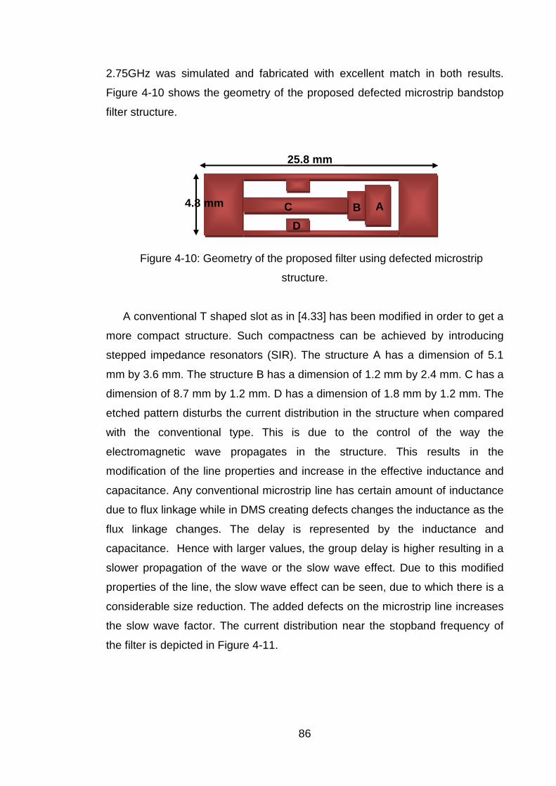
86
2.75GHz was simulated and fabricated with excellent match in both results.
Figure 4-10 shows the geometry of the proposed defected microstrip bandstop
filter structure.
Figure 4-10: Geometry of the proposed filter using defected microstrip
structure.
A conventional T shaped slot as in [4.33] has been modified in order to get a
more compact structure. Such compactness can be achieved by introducing
stepped impedance resonators (SIR). The structure A has a dimension of 5.1
mm by 3.6 mm. The structure B has a dimension of 1.2 mm by 2.4 mm. C has a
dimension of 8.7 mm by 1.2 mm. D has a dimension of 1.8 mm by 1.2 mm. The
etched pattern disturbs the current distribution in the structure when compared
with the conventional type. This is due to the control of the way the
electromagnetic wave propagates in the structure. This results in the
modification of the line properties and increase in the effective inductance and
capacitance. Any conventional microstrip line has certain amount of inductance
due to flux linkage while in DMS creating defects changes the inductance as the
flux linkage changes. The delay is represented by the inductance and
capacitance. Hence with larger values, the group delay is higher resulting in a
slower propagation of the wave or the slow wave effect. Due to this modified
properties of the line, the slow wave effect can be seen, due to which there is a
considerable size reduction. The added defects on the microstrip line increases
the slow wave factor. The current distribution near the stopband frequency of
the filter is depicted in Figure 4-11.
C B A
D
25.8 mm
4.8 mm
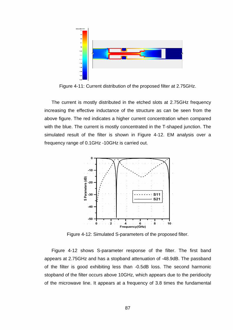
87
Figure 4-11: Current distribution of the proposed filter at 2.75GHz.
The current is mostly distributed in the etched slots at 2.75GHz frequency
increasing the effective inductance of the structure as can be seen from the
above figure. The red indicates a higher current concentration when compared
with the blue. The current is mostly concentrated in the T-shaped junction. The
simulated result of the filter is shown in Figure 4-12. EM analysis over a
frequency range of 0.1GHz -10GHz is carried out.
Figure 4-12: Simulated S-parameters of the proposed filter.
Figure 4-12 shows S-parameter response of the filter. The first band
appears at 2.75GHz and has a stopband attenuation of -48.9dB. The passband
of the filter is good exhibiting less than -0.5dB loss. The second harmonic
stopband of the filter occurs above 10GHz, which appears due to the peridiocity
of the microwave line. It appears at a frequency of 3.8 times the fundamental
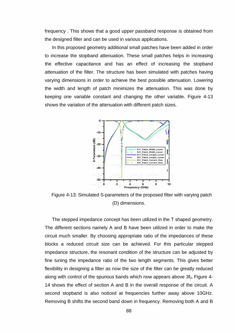
88
frequency . This shows that a good upper passband response is obtained from
the designed filter and can be used in various applications.
In this proposed geometry additional small patches have been added in order
to increase the stopband attenuation. These small patches helps in increasing
the effective capacitance and has an effect of increasing the stopband
attenuation of the filter. The structure has been simulated with patches having
varying dimensions in order to achieve the best possible attenuation. Lowering
the width and length of patch minimizes the attenuation. This was done by
keeping one variable constant and changing the other variable. Figure 4-13
shows the variation of the attenuation with different patch sizes.
Figure 4-13: Simulated S-parameters of the proposed filter with varying patch
(D) dimensions.
The stepped impedance concept has been utilized in the T shaped geometry.
The different sections namely A and B have been utilized in order to make the
circuit much smaller. By choosing appropriate ratio of the impedances of these
blocks a reduced circuit size can be achieved. For this particular stepped
impedance structure, the resonant condition of the structure can be adjusted by
fine tuning the impedance ratio of the two length segments. This gives better
flexibility in designing a filter as now the size of the filter can be greatly reduced
along with control of the spurious bands which now appears above 3f0. Figure 4-
14 shows the effect of section A and B in the overall response of the circuit. A
second stopband is also noticed at frequencies further away above 10GHz.
Removing B shifts the second band down in frequency. Removing both A and B
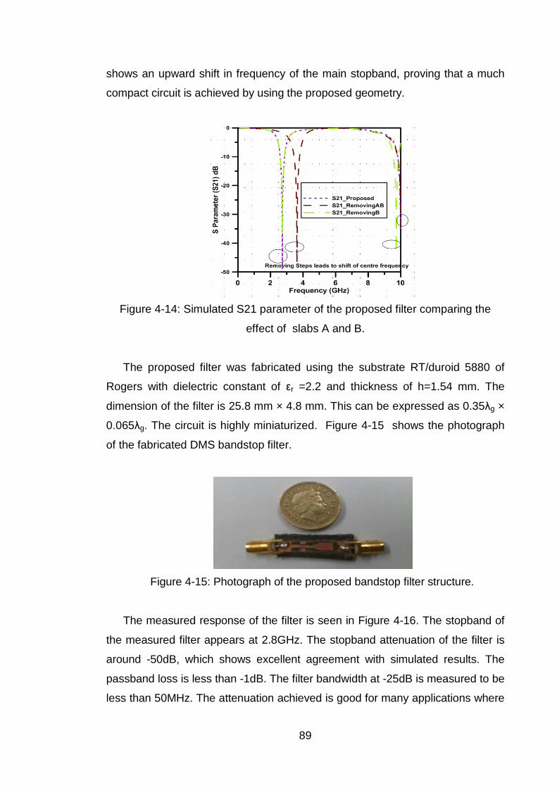
89
shows an upward shift in frequency of the main stopband, proving that a much
compact circuit is achieved by using the proposed geometry.
Figure 4-14: Simulated S21 parameter of the proposed filter comparing the
effect of slabs A and B.
The proposed filter was fabricated using the substrate RT/duroid 5880 of
Rogers with dielectric constant of εr =2.2 and thickness of h=1.54 mm. The
dimension of the filter is 25.8 mm × 4.8 mm. This can be expressed as 0.35λg ×
0.065λg. The circuit is highly miniaturized. Figure 4-15 shows the photograph
of the fabricated DMS bandstop filter.
Figure 4-15: Photograph of the proposed bandstop filter structure.
The measured response of the filter is seen in Figure 4-16. The stopband of
the measured filter appears at 2.8GHz. The stopband attenuation of the filter is
around -50dB, which shows excellent agreement with simulated results. The
passband loss is less than -1dB. The filter bandwidth at -25dB is measured to be
less than 50MHz. The attenuation achieved is good for many applications where

90
unwanted distortion signals need to be filtered out. There is a slight shift of the
centre frequency of the filter. This is because of fabrication tolerances.
Figure 4-16: Measured S-parameters of the proposed bandstop filter.
Figure 4-17: Comparison of measured and simulated S-parameters of the
proposed bandstop filter.
One such novel fixed bandstop filter was created using a new concept of
DMS which showed excellent results. Another example of a bandstop filter is
given below which has been designed to be more compact as compared to the
previous DMS filter. The filter has a 3dB fractional bandwidth of 10%. The
stopband attenuation is around 40dB. The equivalent circuit has been extracted
and experimental results are presented. Furthermore the upper spurious
response occurs nearly 4 times the fundamental frequency. The filter hence has
an extended upper pass band which is beneficial in many applications one of
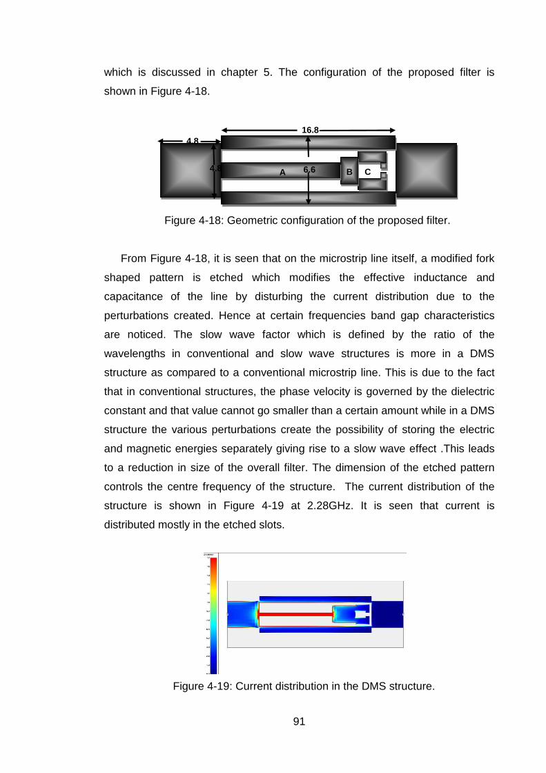
91
which is discussed in chapter 5. The configuration of the proposed filter is
shown in Figure 4-18.
Figure 4-18: Geometric configuration of the proposed filter.
From Figure 4-18, it is seen that on the microstrip line itself, a modified fork
shaped pattern is etched which modifies the effective inductance and
capacitance of the line by disturbing the current distribution due to the
perturbations created. Hence at certain frequencies band gap characteristics
are noticed. The slow wave factor which is defined by the ratio of the
wavelengths in conventional and slow wave structures is more in a DMS
structure as compared to a conventional microstrip line. This is due to the fact
that in conventional structures, the phase velocity is governed by the dielectric
constant and that value cannot go smaller than a certain amount while in a DMS
structure the various perturbations create the possibility of storing the electric
and magnetic energies separately giving rise to a slow wave effect .This leads
to a reduction in size of the overall filter. The dimension of the etched pattern
controls the centre frequency of the structure. The current distribution of the
structure is shown in Figure 4-19 at 2.28GHz. It is seen that current is
distributed mostly in the etched slots.
Figure 4-19: Current distribution in the DMS structure.
16.8
A B C 6.6
4.8
4.8
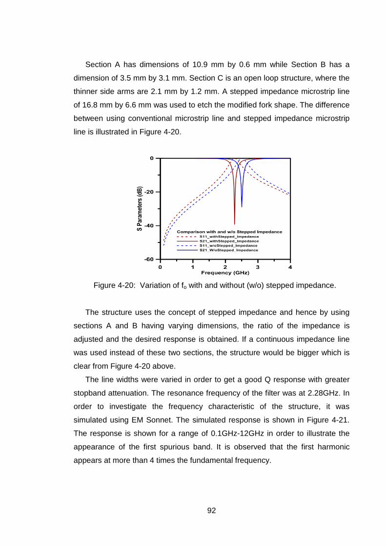
92
Section A has dimensions of 10.9 mm by 0.6 mm while Section B has a
dimension of 3.5 mm by 3.1 mm. Section C is an open loop structure, where the
thinner side arms are 2.1 mm by 1.2 mm. A stepped impedance microstrip line
of 16.8 mm by 6.6 mm was used to etch the modified fork shape. The difference
between using conventional microstrip line and stepped impedance microstrip
line is illustrated in Figure 4-20.
Figure 4-20: Variation of fo with and without (w/o) stepped impedance.
The structure uses the concept of stepped impedance and hence by using
sections A and B having varying dimensions, the ratio of the impedance is
adjusted and the desired response is obtained. If a continuous impedance line
was used instead of these two sections, the structure would be bigger which is
clear from Figure 4-20 above.
The line widths were varied in order to get a good Q response with greater
stopband attenuation. The resonance frequency of the filter was at 2.28GHz. In
order to investigate the frequency characteristic of the structure, it was
simulated using EM Sonnet. The simulated response is shown in Figure 4-21.
The response is shown for a range of 0.1GHz-12GHz in order to illustrate the
appearance of the first spurious band. It is observed that the first harmonic
appears at more than 4 times the fundamental frequency.
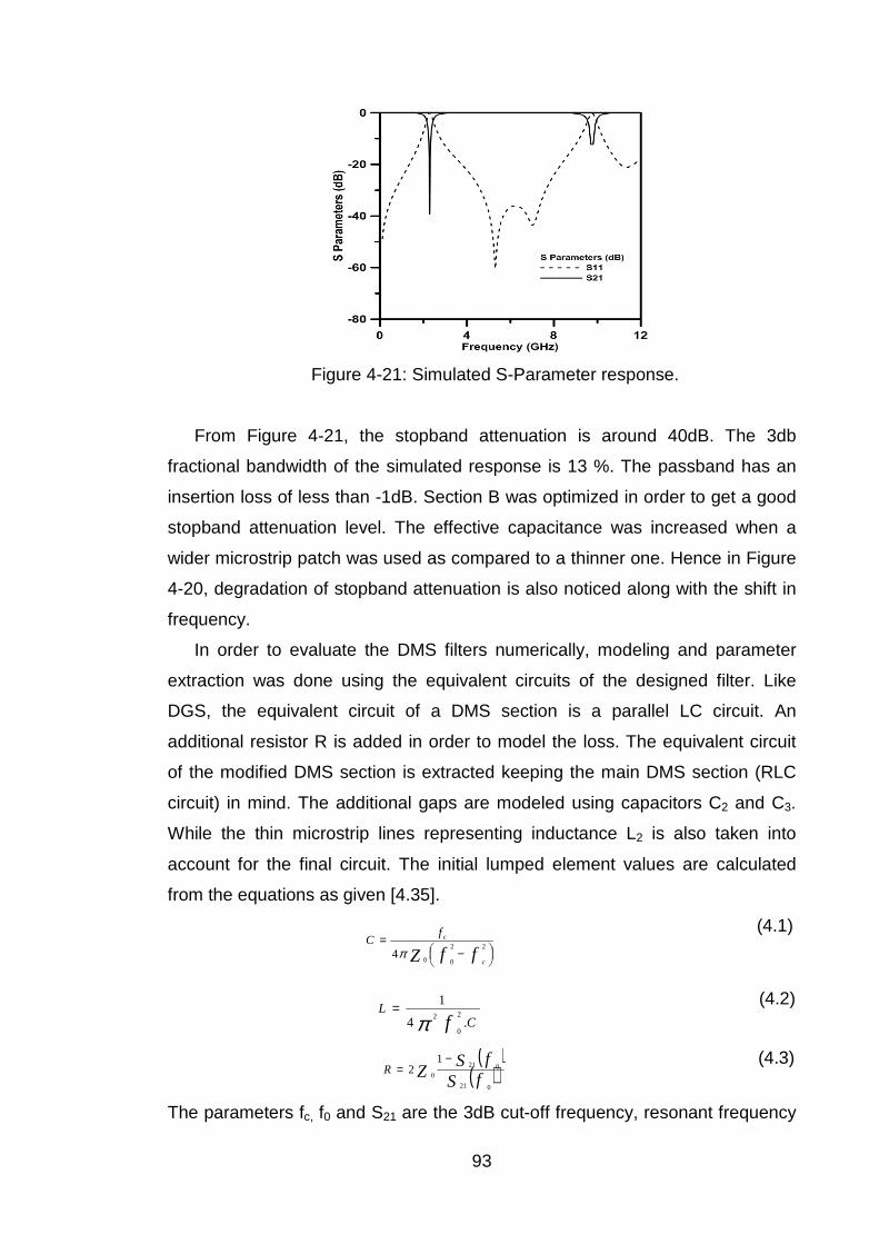
93
Figure 4-21: Simulated S-Parameter response.
From Figure 4-21, the stopband attenuation is around 40dB. The 3db
fractional bandwidth of the simulated response is 13 %. The passband has an
insertion loss of less than -1dB. Section B was optimized in order to get a good
stopband attenuation level. The effective capacitance was increased when a
wider microstrip patch was used as compared to a thinner one. Hence in Figure
4-20, degradation of stopband attenuation is also noticed along with the shift in
frequency.
In order to evaluate the DMS filters numerically, modeling and parameter
extraction was done using the equivalent circuits of the designed filter. Like
DGS, the equivalent circuit of a DMS section is a parallel LC circuit. An
additional resistor R is added in order to model the loss. The equivalent circuit
of the modified DMS section is extracted keeping the main DMS section (RLC
circuit) in mind. The additional gaps are modeled using capacitors C2 and C3.
While the thin microstrip lines representing inductance L2 is also taken into
account for the final circuit. The initial lumped element values are calculated
from the equations as given [4.35].
−
=ffZ c
cfC
22
004π
(4.1)
C
Lf .4
12
0
2π= (4.2)
( )( )fS
fSZR
021
021
0
12
−=
(4.3)
The parameters fc, f0 and S21 are the 3dB cut-off frequency, resonant frequency
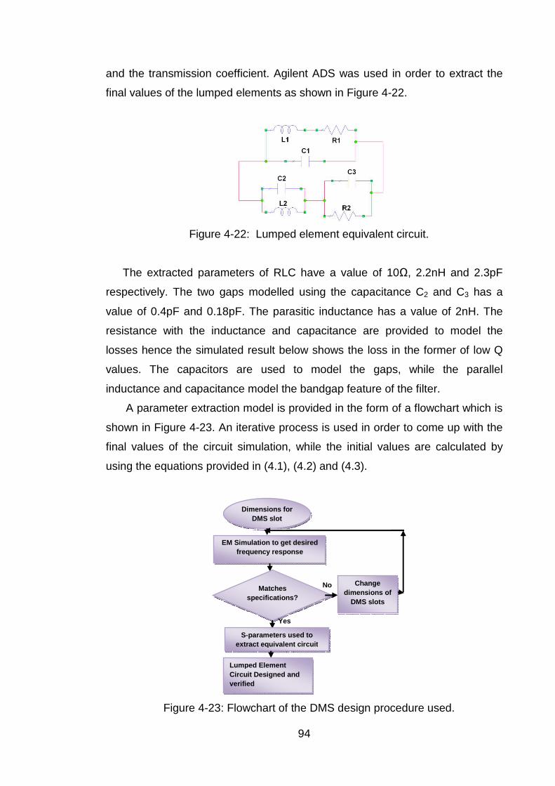
94
and the transmission coefficient. Agilent ADS was used in order to extract the
final values of the lumped elements as shown in Figure 4-22.
Figure 4-22: Lumped element equivalent circuit.
The extracted parameters of RLC have a value of 10Ω, 2.2nH and 2.3pF
respectively. The two gaps modelled using the capacitance C2 and C3 has a
value of 0.4pF and 0.18pF. The parasitic inductance has a value of 2nH. The
resistance with the inductance and capacitance are provided to model the
losses hence the simulated result below shows the loss in the former of low Q
values. The capacitors are used to model the gaps, while the parallel
inductance and capacitance model the bandgap feature of the filter.
A parameter extraction model is provided in the form of a flowchart which is
shown in Figure 4-23. An iterative process is used in order to come up with the
final values of the circuit simulation, while the initial values are calculated by
using the equations provided in (4.1), (4.2) and (4.3).
Figure 4-23: Flowchart of the DMS design procedure used.
Dimensions for DMS slot
EM Simulation to get desired frequency response
Matches specifications?
Change dimensions of
DMS slots
No
Yes
S-parameters used to extract equivalent circuit
Lumped Element Circuit Designed and verified
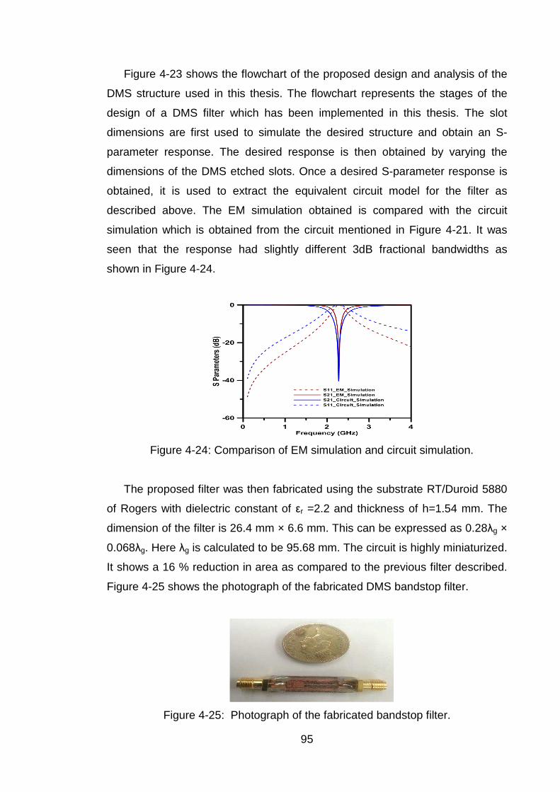
95
Figure 4-23 shows the flowchart of the proposed design and analysis of the
DMS structure used in this thesis. The flowchart represents the stages of the
design of a DMS filter which has been implemented in this thesis. The slot
dimensions are first used to simulate the desired structure and obtain an S-
parameter response. The desired response is then obtained by varying the
dimensions of the DMS etched slots. Once a desired S-parameter response is
obtained, it is used to extract the equivalent circuit model for the filter as
described above. The EM simulation obtained is compared with the circuit
simulation which is obtained from the circuit mentioned in Figure 4-21. It was
seen that the response had slightly different 3dB fractional bandwidths as
shown in Figure 4-24.
Figure 4-24: Comparison of EM simulation and circuit simulation.
The proposed filter was then fabricated using the substrate RT/Duroid 5880
of Rogers with dielectric constant of εr =2.2 and thickness of h=1.54 mm. The
dimension of the filter is 26.4 mm × 6.6 mm. This can be expressed as 0.28λg ×
0.068λg. Here λg is calculated to be 95.68 mm. The circuit is highly miniaturized.
It shows a 16 % reduction in area as compared to the previous filter described.
Figure 4-25 shows the photograph of the fabricated DMS bandstop filter.
Figure 4-25: Photograph of the fabricated bandstop filter.
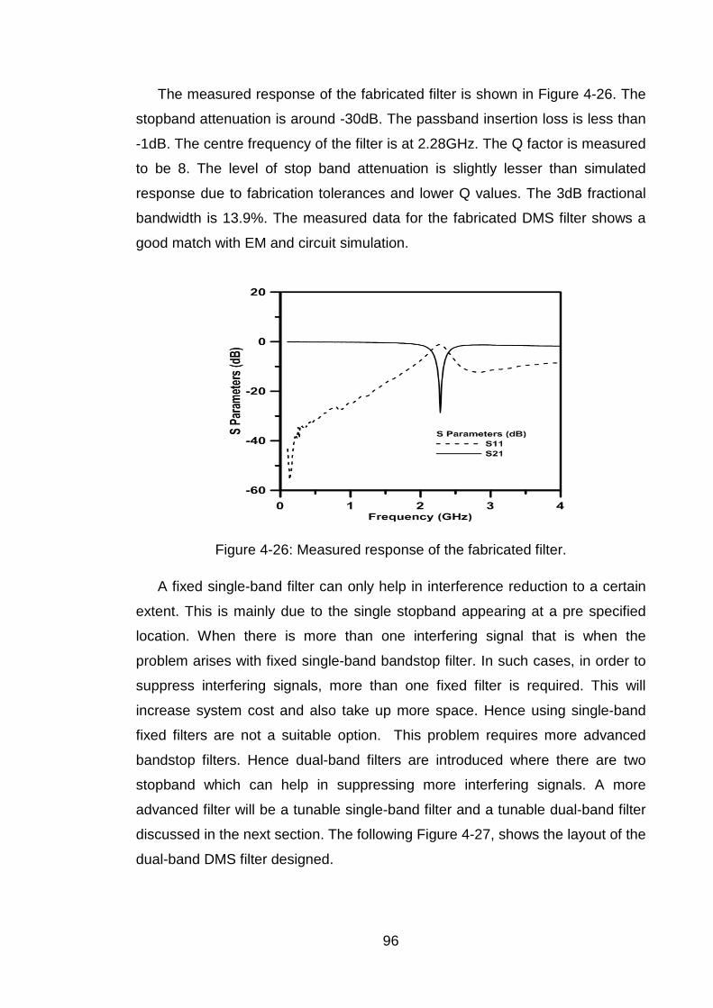
96
The measured response of the fabricated filter is shown in Figure 4-26. The
stopband attenuation is around -30dB. The passband insertion loss is less than
-1dB. The centre frequency of the filter is at 2.28GHz. The Q factor is measured
to be 8. The level of stop band attenuation is slightly lesser than simulated
response due to fabrication tolerances and lower Q values. The 3dB fractional
bandwidth is 13.9%. The measured data for the fabricated DMS filter shows a
good match with EM and circuit simulation.
Figure 4-26: Measured response of the fabricated filter.
A fixed single-band filter can only help in interference reduction to a certain
extent. This is mainly due to the single stopband appearing at a pre specified
location. When there is more than one interfering signal that is when the
problem arises with fixed single-band bandstop filter. In such cases, in order to
suppress interfering signals, more than one fixed filter is required. This will
increase system cost and also take up more space. Hence using single-band
fixed filters are not a suitable option. This problem requires more advanced
bandstop filters. Hence dual-band filters are introduced where there are two
stopband which can help in suppressing more interfering signals. A more
advanced filter will be a tunable single-band filter and a tunable dual-band filter
discussed in the next section. The following Figure 4-27, shows the layout of the
dual-band DMS filter designed.
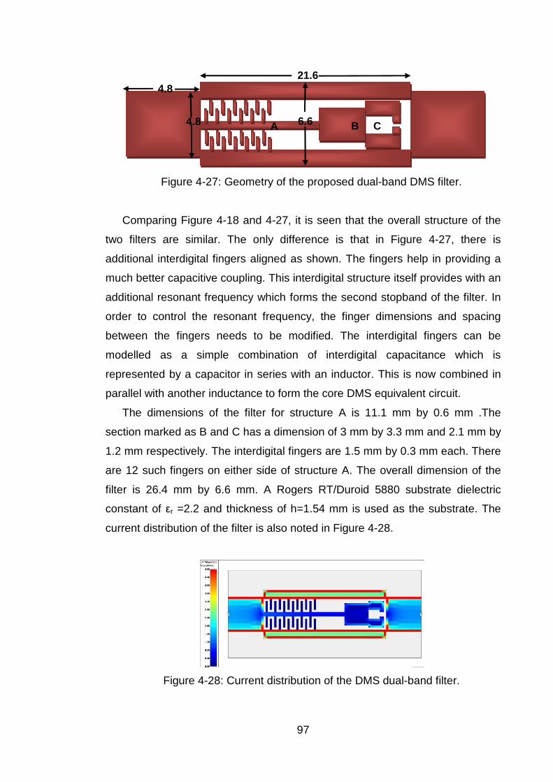
97
Figure 4-27: Geometry of the proposed dual-band DMS filter.
Comparing Figure 4-18 and 4-27, it is seen that the overall structure of the
two filters are similar. The only difference is that in Figure 4-27, there is
additional interdigital fingers aligned as shown. The fingers help in providing a
much better capacitive coupling. This interdigital structure itself provides with an
additional resonant frequency which forms the second stopband of the filter. In
order to control the resonant frequency, the finger dimensions and spacing
between the fingers needs to be modified. The interdigital fingers can be
modelled as a simple combination of interdigital capacitance which is
represented by a capacitor in series with an inductor. This is now combined in
parallel with another inductance to form the core DMS equivalent circuit.
The dimensions of the filter for structure A is 11.1 mm by 0.6 mm .The
section marked as B and C has a dimension of 3 mm by 3.3 mm and 2.1 mm by
1.2 mm respectively. The interdigital fingers are 1.5 mm by 0.3 mm each. There
are 12 such fingers on either side of structure A. The overall dimension of the
filter is 26.4 mm by 6.6 mm. A Rogers RT/Duroid 5880 substrate dielectric
constant of εr =2.2 and thickness of h=1.54 mm is used as the substrate. The
current distribution of the filter is also noted in Figure 4-28.
Figure 4-28: Current distribution of the DMS dual-band filter.
21.6
A B C 6.6
4.8
4.8
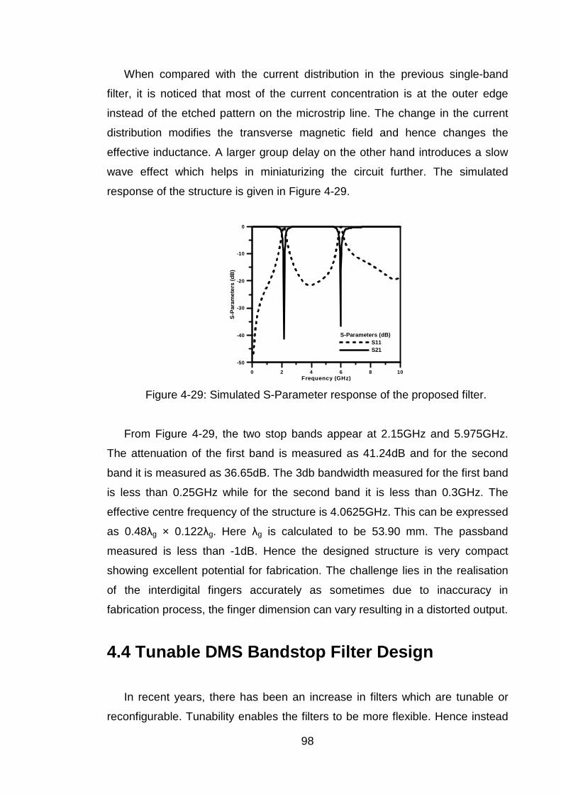
98
When compared with the current distribution in the previous single-band
filter, it is noticed that most of the current concentration is at the outer edge
instead of the etched pattern on the microstrip line. The change in the current
distribution modifies the transverse magnetic field and hence changes the
effective inductance. A larger group delay on the other hand introduces a slow
wave effect which helps in miniaturizing the circuit further. The simulated
response of the structure is given in Figure 4-29.
0 2 4 6 8 10Frequency (GHz)
-50
-40
-30
-20
-10
0S
-Par
amet
ers
(dB
)
S-Parameters (dB)S11S21
Figure 4-29: Simulated S-Parameter response of the proposed filter.
From Figure 4-29, the two stop bands appear at 2.15GHz and 5.975GHz.
The attenuation of the first band is measured as 41.24dB and for the second
band it is measured as 36.65dB. The 3db bandwidth measured for the first band
is less than 0.25GHz while for the second band it is less than 0.3GHz. The
effective centre frequency of the structure is 4.0625GHz. This can be expressed
as 0.48λg × 0.122λg. Here λg is calculated to be 53.90 mm. The passband
measured is less than -1dB. Hence the designed structure is very compact
showing excellent potential for fabrication. The challenge lies in the realisation
of the interdigital fingers accurately as sometimes due to inaccuracy in
fabrication process, the finger dimension can vary resulting in a distorted output.
4.4 Tunable DMS Bandstop Filter Design
In recent years, there has been an increase in filters which are tunable or
reconfigurable. Tunability enables the filters to be more flexible. Hence instead
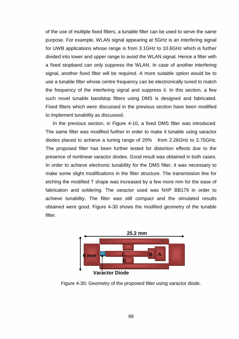
99
of the use of multiple fixed filters, a tunable filter can be used to serve the same
purpose. For example, WLAN signal appearing at 5GHz is an interfering signal
for UWB applications whose range is from 3.1GHz to 10.6GHz which is further
divided into lower and upper range to avoid the WLAN signal. Hence a filter with
a fixed stopband can only suppress the WLAN. In case of another interfering
signal, another fixed filter will be required. A more suitable option would be to
use a tunable filter whose centre frequency can be electronically tuned to match
the frequency of the interfering signal and suppress it. In this section, a few
such novel tunable bandstop filters using DMS is designed and fabricated.
Fixed filters which were discussed in the previous section have been modified
to implement tunability as discussed.
In the previous section, in Figure 4-10, a fixed DMS filter was introduced.
The same filter was modified further in order to make it tunable using varactor
diodes placed to achieve a tuning range of 20% from 2.26GHz to 2.75GHz.
The proposed filter has been further tested for distortion effects due to the
presence of nonlinear varactor diodes. Good result was obtained in both cases.
In order to achieve electronic tunability for the DMS filter, it was necessary to
make some slight modifications in the filter structure. The transmission line for
etching the modified T shape was increased by a few more mm for the ease of
fabrication and soldering. The varactor used was NXP BB179 in order to
achieve tunability. The filter was still compact and the simulated results
obtained were good. Figure 4-30 shows the modified geometry of the tunable
filter.
Figure 4-30: Geometry of the proposed filter using varactor diode.
C B A
Varactor Diode
25.2 mm
D 6 mm
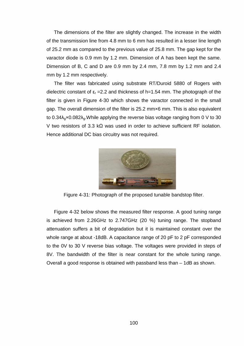
100
The dimensions of the filter are slightly changed. The increase in the width
of the transmission line from 4.8 mm to 6 mm has resulted in a lesser line length
of 25.2 mm as compared to the previous value of 25.8 mm. The gap kept for the
varactor diode is 0.9 mm by 1.2 mm. Dimension of A has been kept the same.
Dimension of B, C and D are 0.9 mm by 2.4 mm, 7.8 mm by 1.2 mm and 2.4
mm by 1.2 mm respectively.
The filter was fabricated using substrate RT/Duroid 5880 of Rogers with
dielectric constant of εr =2.2 and thickness of h=1.54 mm. The photograph of the
filter is given in Figure 4-30 which shows the varactor connected in the small
gap. The overall dimension of the filter is 25.2 mm×6 mm. This is also equivalent
to 0.34λg×0.082λg.While applying the reverse bias voltage ranging from 0 V to 30
V two resistors of 3.3 kΩ was used in order to achieve sufficient RF isolation.
Hence additional DC bias circuitry was not required.
Figure 4-31: Photograph of the proposed tunable bandstop filter.
Figure 4-32 below shows the measured filter response. A good tuning range
is achieved from 2.26GHz to 2.747GHz (20 %) tuning range. The stopband
attenuation suffers a bit of degradation but it is maintained constant over the
whole range at about -18dB. A capacitance range of 20 pF to 2 pF corresponded
to the 0V to 30 V reverse bias voltage. The voltages were provided in steps of
8V. The bandwidth of the filter is near constant for the whole tuning range.
Overall a good response is obtained with passband less than – 1dB as shown.
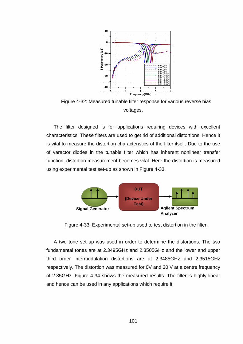
101
Figure 4-32: Measured tunable filter response for various reverse bias
voltages.
The filter designed is for applications requiring devices with excellent
characteristics. These filters are used to get rid of additional distortions. Hence it
is vital to measure the distortion characteristics of the filter itself. Due to the use
of varactor diodes in the tunable filter which has inherent nonlinear transfer
function, distortion measurement becomes vital. Here the distortion is measured
using experimental test set-up as shown in Figure 4-33.
Figure 4-33: Experimental set-up used to test distortion in the filter.
A two tone set up was used in order to determine the distortions. The two
fundamental tones are at 2.3495GHz and 2.3505GHz and the lower and upper
third order intermodulation distortions are at 2.3485GHz and 2.3515GHz
respectively. The distortion was measured for 0V and 30 V at a centre frequency
of 2.35GHz. Figure 4-34 shows the measured results. The filter is highly linear
and hence can be used in any applications which require it.
DUT
(Device Under Test)
Signal Generator Agilent Spectrum Analyzer
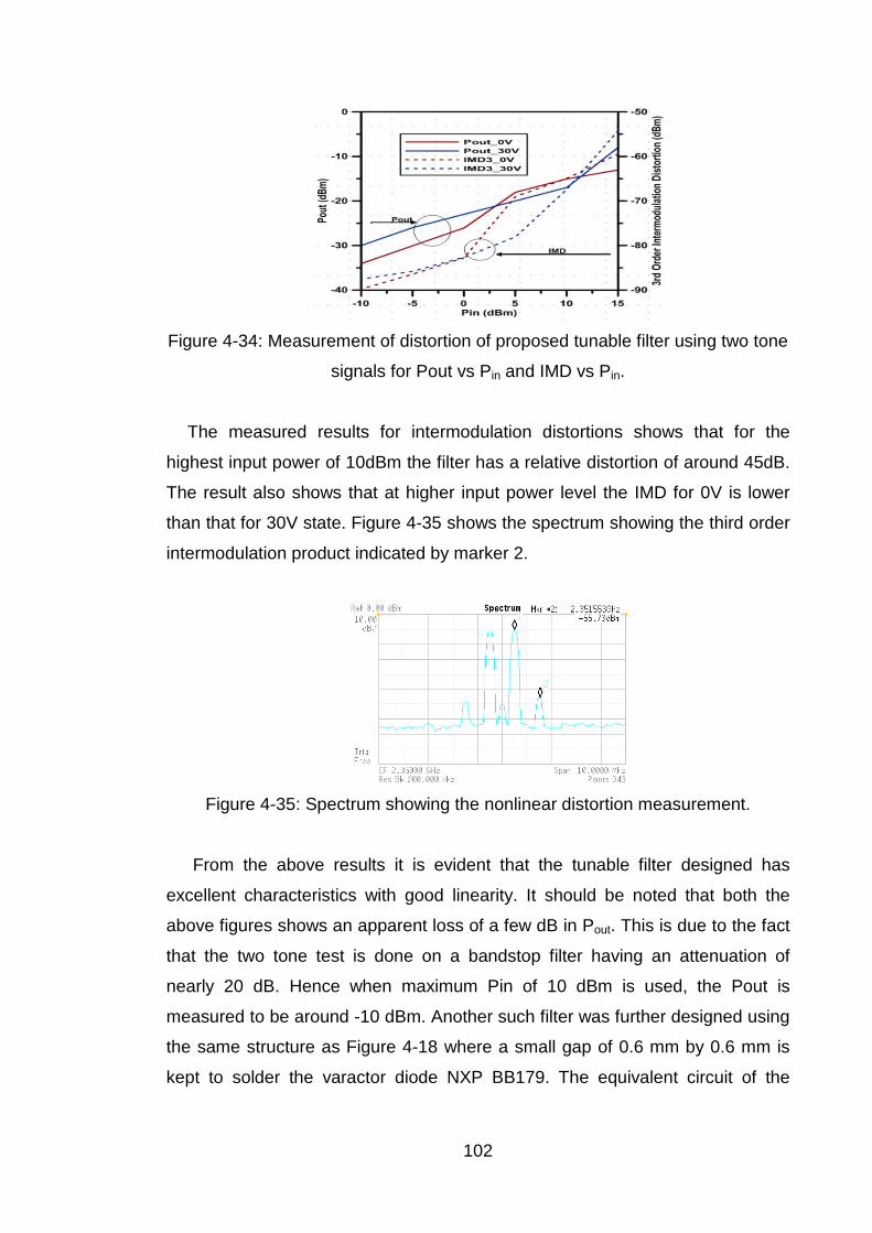
102
Figure 4-34: Measurement of distortion of proposed tunable filter using two tone
signals for Pout vs Pin and IMD vs Pin.
The measured results for intermodulation distortions shows that for the
highest input power of 10dBm the filter has a relative distortion of around 45dB.
The result also shows that at higher input power level the IMD for 0V is lower
than that for 30V state. Figure 4-35 shows the spectrum showing the third order
intermodulation product indicated by marker 2.
Figure 4-35: Spectrum showing the nonlinear distortion measurement.
From the above results it is evident that the tunable filter designed has
excellent characteristics with good linearity. It should be noted that both the
above figures shows an apparent loss of a few dB in Pout. This is due to the fact
that the two tone test is done on a bandstop filter having an attenuation of
nearly 20 dB. Hence when maximum Pin of 10 dBm is used, the Pout is
measured to be around -10 dBm. Another such filter was further designed using
the same structure as Figure 4-18 where a small gap of 0.6 mm by 0.6 mm is
kept to solder the varactor diode NXP BB179. The equivalent circuit of the
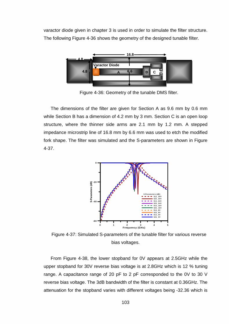
103
varactor diode given in chapter 3 is used in order to simulate the filter structure.
The following Figure 4-36 shows the geometry of the designed tunable filter.
Figure 4-36: Geometry of the tunable DMS filter.
The dimensions of the filter are given for Section A as 9.6 mm by 0.6 mm
while Section B has a dimension of 4.2 mm by 3 mm. Section C is an open loop
structure, where the thinner side arms are 2.1 mm by 1.2 mm. A stepped
impedance microstrip line of 16.8 mm by 6.6 mm was used to etch the modified
fork shape. The filter was simulated and the S-parameters are shown in Figure
4-37.
0 1 2 3 4 5Frequency (GHz)
-60
-40
-20
0
S-P
aram
eter
s (d
B)
S-Param ete rs (dB )S11_30VS21_30VS11_24VS21_24VS11_16VS21_16VS11_8VS21_8VS11_0VS21_0V
Figure 4-37: Simulated S-parameters of the tunable filter for various reverse
bias voltages.
From Figure 4-38, the lower stopband for 0V appears at 2.5GHz while the
upper stopband for 30V reverse bias voltage is at 2.8GHz which is 12 % tuning
range. A capacitance range of 20 pF to 2 pF corresponded to the 0V to 30 V
reverse bias voltage. The 3dB bandwidth of the filter is constant at 0.36GHz. The
attenuation for the stopband varies with different voltages being -32.36 which is
16.8
A B C 6.6
4.8
4.8
Varactor Diode

104
the maximum at 30V. The stopband attenuation for all other reverse bias
voltages is more than -25dB. The passband of the filter is noted to be always
less than -1dB showing excellent results.
The filter was designed using substrate RT/Duroid 5880 of Rogers with
dielectric constant of εr =2.2 and thickness of h=1.54 mm. The overall dimension
of the filter is 26.4 mm×6.6 mm. This is also equivalent to 0.321λg×0.080λg. This
shows that the filter size for the tunable DMS mentioned in Figure 4-35 is better
than the filter in Figure 4-30. This filter can be further fabricated and tested for
distortions.
The third tunable filter which is discussed in this section is that of a dual-band
tunable filter. Tunable dual-band filters have a much wider application when
compared to single-band tunable filters. The main reason for that is that a lot
more flexibility and control is given to the user. In the previous section, an
example of the fixed dual-band filter was given in Figure 4-27. The same filter
was modified in order to incorporate a tuning element, a varactor in this case. A
varactor model NXP BB179 was used in order to electronically tune the
stopbands. Figure 4-38 shows the geometry of the tunable dual-band DMS filter.
Figure 4-38: Geometry of the proposed tunable dual-band DMS filter.
The filter dimensions undergo a slight modification in order to incorporate
the varactor diode. A gap of 0.6 mm by 0.6 mm is kept for the varactor diode as
shown in Figure 4-38. The interdigital fingers are changed from twelve to eleven
in number. This leads to the change in the resonant frequency of the second
band. The dimensions of the filter for structure A is 10.5 mm by 0.6 mm .The
section marked as B and C has a dimension of 3 mm by 3.3 mm and 2.1 mm by
1.2 mm respectively. The interdigital fingers are 1.5 mm by 0.3 mm each. The
21.6
A B C 6.6
4.8
4.8 Varactor Diode
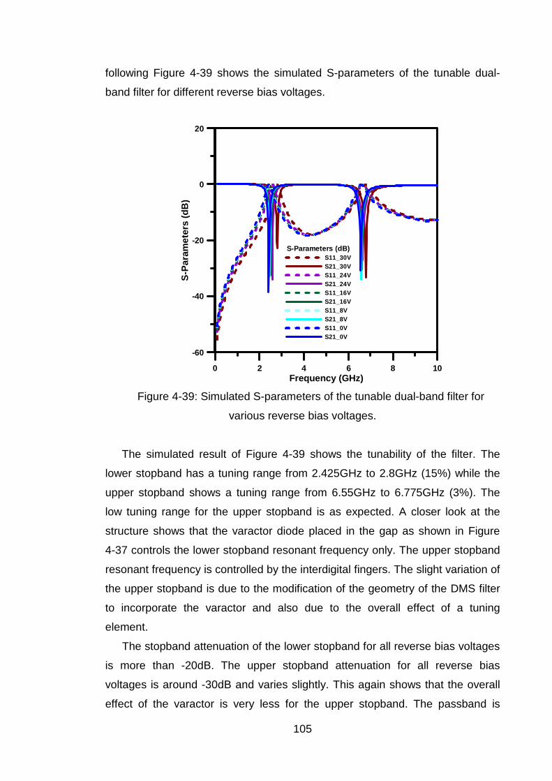
105
following Figure 4-39 shows the simulated S-parameters of the tunable dual-
band filter for different reverse bias voltages.
0 2 4 6 8 10Frequency (GHz)
-60
-40
-20
0
20
S-P
aram
eter
s (d
B)
S-Parameters (dB)S11_30VS21_30VS11_24VS21_24VS11_16VS21_16VS11_8VS21_8VS11_0VS21_0V
Figure 4-39: Simulated S-parameters of the tunable dual-band filter for
various reverse bias voltages.
The simulated result of Figure 4-39 shows the tunability of the filter. The
lower stopband has a tuning range from 2.425GHz to 2.8GHz (15%) while the
upper stopband shows a tuning range from 6.55GHz to 6.775GHz (3%). The
low tuning range for the upper stopband is as expected. A closer look at the
structure shows that the varactor diode placed in the gap as shown in Figure
4-37 controls the lower stopband resonant frequency only. The upper stopband
resonant frequency is controlled by the interdigital fingers. The slight variation of
the upper stopband is due to the modification of the geometry of the DMS filter
to incorporate the varactor and also due to the overall effect of a tuning
element.
The stopband attenuation of the lower stopband for all reverse bias voltages
is more than -20dB. The upper stopband attenuation for all reverse bias
voltages is around -30dB and varies slightly. This again shows that the overall
effect of the varactor is very less for the upper stopband. The passband is
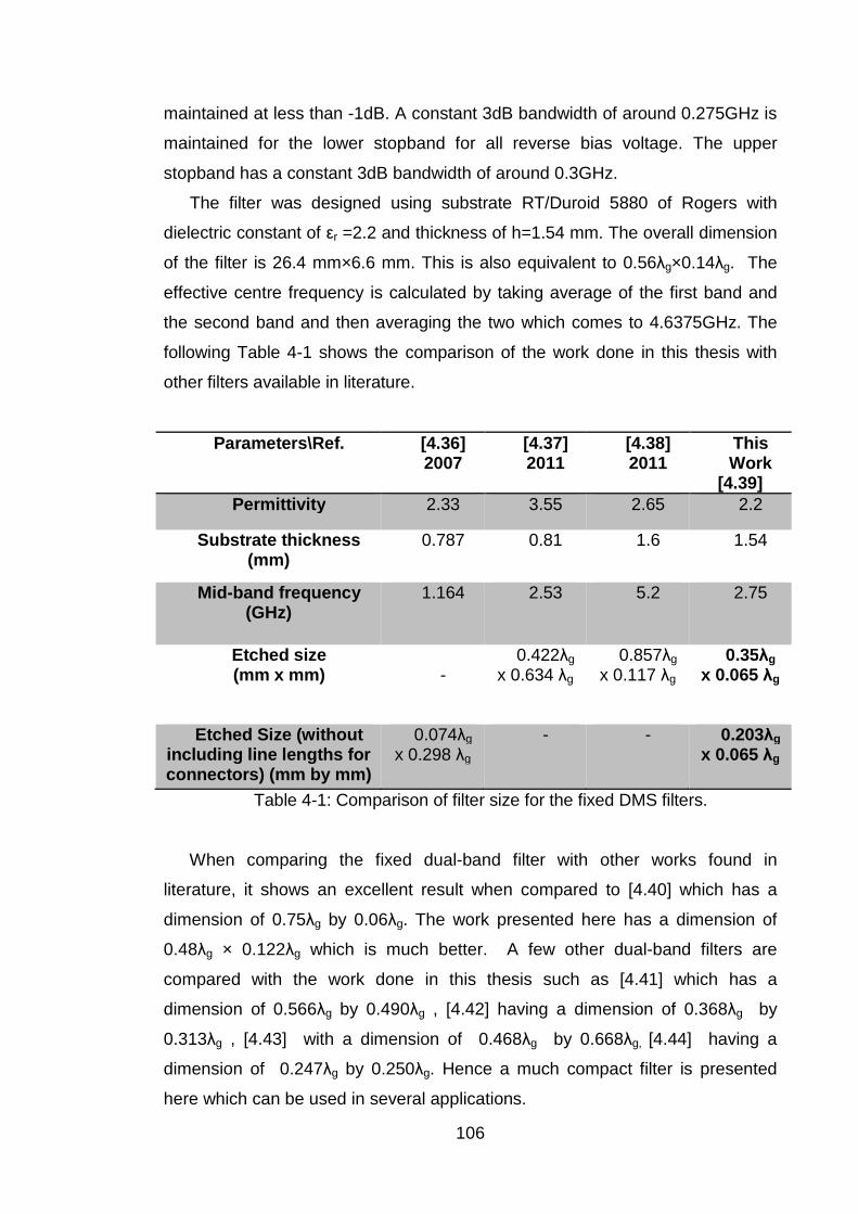
106
maintained at less than -1dB. A constant 3dB bandwidth of around 0.275GHz is
maintained for the lower stopband for all reverse bias voltage. The upper
stopband has a constant 3dB bandwidth of around 0.3GHz.
The filter was designed using substrate RT/Duroid 5880 of Rogers with
dielectric constant of εr =2.2 and thickness of h=1.54 mm. The overall dimension
of the filter is 26.4 mm×6.6 mm. This is also equivalent to 0.56λg×0.14λg. The
effective centre frequency is calculated by taking average of the first band and
the second band and then averaging the two which comes to 4.6375GHz. The
following Table 4-1 shows the comparison of the work done in this thesis with
other filters available in literature.
Parameters \Ref. [4.36] 2007
[4.37] 2011
[4.38] 2011
This Work
[4.39] Permittivity 2.33 3.55 2.65 2.2
Substrate thickness (mm)
0.787 0.81 1.6 1.54
Mid-band frequency (GHz)
1.164 2.53 5.2 2.75
Etched size (mm x mm)
-
0.422λg x 0.634 λg
0.857λg x 0.117 λg
0.35λg x 0.065 λg
Etched Size (without including line lengths for connectors) (mm by mm)
0.074λg x 0.298 λg
- - 0.203λg x 0.065 λg
Table 4-1: Comparison of filter size for the fixed DMS filters.
When comparing the fixed dual-band filter with other works found in
literature, it shows an excellent result when compared to [4.40] which has a
dimension of 0.75λg by 0.06λg. The work presented here has a dimension of
0.48λg × 0.122λg which is much better. A few other dual-band filters are
compared with the work done in this thesis such as [4.41] which has a
dimension of 0.566λg by 0.490λg , [4.42] having a dimension of 0.368λg by
0.313λg , [4.43] with a dimension of 0.468λg by 0.668λg, [4.44] having a
dimension of 0.247λg by 0.250λg. Hence a much compact filter is presented
here which can be used in several applications.
107
4.4 Conclusion
This chapter gives an overview of the microstrip bandstop filter and briefly
discusses the relevant applications. The importance of the BSF lies in the
suppression of interfering signals in this thesis. A brief summary of conventional
microstrip bandstop filter is given along with a few examples which include
single-band and dual-band bandstop filters as well as tunable filters.
Defected microstrip structure being a new way of designing bandstop filter is
discussed and a brief literature review is provided. Several different structures
of bandstop filter using DMS is presented. Two such novel fixed single-band
bandstop filters were presented along with experimental verification. The filters
were highly miniaturized with excellent stopband attenuation and passband
characteristics. A novel dual-band fixed bandstop filter is also presented which
had attenuations of more than -30dB for both bands.
Tunable bandstop filters using DMS are also provided. One such filter was
fabricated and tested for further distortions. Tuning element used for the filter
was a varactor having inherent nonlinear properties. Hence the filter was
measured for distortion and good linearity was observed. An example of a
novel tunable dual-band filter was also provided. The filters presented in this
thesis were highly miniaturized and the size was further compared with other
such filters available in literature.
108
4.5 References [4.1] R.L. Sleven A. J. Anselmo, D. S. Levinson, J.J. Taub and N. Worontzoff,
"Bandstop Filter Design for Ultra-Low Loss and High Power," Microwave
Conference, 1973. 3rd European, vol.1, no., pp.1, 4, 4-7 Sept. 1973.
[4.2] L. Young, G.L. Matthaei and E.M.T. Jones, “Microwave Bandstop Filters
with Narrow Stop Bands”, PGMTT National Symposium Digest vol: 62, no: 1,
pp: 46 – 51.
[4.3] E.G. Cristal, L. Young, B.M. Schiffman and D.B. Weller, “Bandstop Filter
Formulas (Correspondence)," Microwave Theory and Techniques, IEEE
Transactions on, vol.15, no.3, pp.195, 195, March 1967.
[4.4] P.A. Dupuis, E.G. Cristal, "Folded-Line and Hybrid Folded-Line Bandstop
Filters," Microwave Symposium Digest, 1974 S-MTT International, vol.74, no.1,
pp.162, 164, 12-14 June 1974.
[4.5] R.E. Pearson, "Novel microstrip bandstop filter," Electronics Letters,
vol.13, no.19, pp.561, 562, September 15 1977.
[4.6] R. N. Bates, "Design of microstrip spur-line band-stop filters," Microwaves,
Optics and Acoustics, IEE Journal on, vol.1, no.6, pp.209, 214, November 1977.
[4.7] P. Guillon, S. Mekerta and Y. Garault, "Microstrip bandstop filter using a
dielectric resonator," Microwaves, Optics and Antennas, IEE Proceedings H,
vol.128, no.3, pp.151, 154, June 1981.
[4.8] S. Amari and U. Rosenberg, “Direct synthesis of a new class of bandstop
filters,” IEEE Trans. Microwave Theory Tech., vol. 52, pp. 607-616, February
2004.
[4.9] R.J. Cameron, Ying Wang and Ming Yu, "Direct-coupled realizations for
microwave bandstop filters," Microwave Symposium Digest, 2005 IEEE MTT-S
International , vol., no., pp.4 pp.,, 12-17 June 2005.
[4.10] L. Cheng-Jung, K. M K H Leong, and T. Itoh, "Metamaterial Transmission
Line Based Bandstop and Bandpass Filter Designs Using Broadband Phase
Cancellation," Microwave Symposium Digest, 2006. IEEE MTT-S International,
vol., no., pp.935, 938, 11-16 June 2006.
[4.11] D. R. Jachowski, “Passive Enhancement of Resonator Q in Microwave
Notch Filters” IEEE MTT-S, Digest, 2004.

109
[4.12] D. R. Jachowski, “Compact Frequency-Agile, Absorptive Bandstop
Filters” IEEE MTT-S, Digest, 2005.
[4.13] D.R. Jachowski and A.C. Guyette “Sub-Octave-Tunable Microstrip Notch
Filter” IEEE International Symposium on Electromagnetic Compatibility, 2009.
[4.14] D. R. Jachowski, "Cascadable lossy passive biquad bandstop filter." In
Microwave Symposium Digest, 2006. IEEE MTT-S International, pp. 1213-1216.
IEEE, 2006.
[4.15] A. C. Guyette, I. C. Hunter, D. P. Roger, and D. R. Jachowski. "Perfectly-
matched bandstop filters using lossy resonators." In Microwave Symposium
Digest, 2005 IEEE MTT-S International, pp. 4-pp. IEEE, 2005.
[4.16] F. Frezza, L. Pajewski, and G. Schettini. "Fractal two-dimensional
electromagnetic bandgap structures." Microwave Theory and Techniques, IEEE
Transactions on 52, no. 1 (2004): 220-227.
[4.17] J. D. Joannopoulos, S. G. Johnson, J. N. Winn, and R. D. Meade
Photonic Crystals Moulding the Flow of Light , Princeton, 2008.
[4.18] L. Pajewski and G. Schettini, "Photonic Band-Gap Structures with
Periodicity Interruptions: Theory and Applications," Transparent Optical
Networks, 2007. ICTON '07. 9th International Conference on, vol.2, no., pp.88,
91, 1-5 July 2007.
[4.19] F. Frezza, L. Pajewski and G. Schettini, "Periodic defects in 2D-PBG
materials: full-wave analysis and design," Nanotechnology, IEEE Transactions
on, vol.2, no.3, pp.126, 134, Sept. 2003.
[4.20] H.C.C. Fernandes, A.R.B. Rocha and A. Teixeira, "Analysis of antennas
with PBG substrate," Microwave and Optoelectronics Conference, 2003. IMOC
2003. Proceedings of the 2003 SBMO/IEEE MTT-S International , vol.1, no.,
pp.207,209 vol.1, 20-23 Sept. 2003.
[4.21] W. Y. Leung, R. Biswas, S. D. Cheng, M. M. Sigalas, S. McCalmont, G.
Tuttle, and K.-M. Ho, “Slot antennas on photonic band gap crystals,” IEEE
Trans. Antennas Propagat., vol. 45, pp. 1569–1570, Oct. 1997.
[4.22] S. T. Chew and T. Itoh, “PBG-excited split-mode resonator bandpass
filter,” IEEE Microwave Wireless Comp. Lett., vol. 11, pp. 364–366,Sept. 2001.
[4.23] P. Dansas, N. A. Paraire, and S. Laval, “Feasibility of optical filters and
switches using plastic photonic bandgap structures”, Proc. SPIE, vol.3135, pp.
219–229, 1997.
110
[4.24] J. G. Maloney, M. P. Kesler, B. L. Shirley, and G. S. Smith, “A simple
description for waveguiding in photonic bandgap materials,” MicrowaveOpt.
Technol. Lett., vol. 14, pp. 261–266, Apr. 1997.
[4.25] X. Wang, B.Wang, H. Zhang, and K.J.Shen, “A Tunable Bandstop
Resonator Based on a Compact Slotted Ground Structure”, Microwave Theory
and Techniques, IEEE Transactions on, vol.55, no.9, pp.1912-1918, Sept.
2007.
[4.26] D. Ahn, J. Park, C. Kim, J. Kim, J. Qian and T. Itoh, "A design of the low-
pass filter using the novel microstrip defected ground structure," Microwave
Theory and Techniques, IEEE Transactions on , vol.49, no.1, pp.86-93, Jan
2001.
[4.27] D. Woo, T. Lee, J. Lee, C. Pyo and W. Choi, "Novel U-slot and V-slot
DGSs for bandstop filter with improved Q factor," Microwave Theory and
Techniques, IEEE Transactions on , vol.54, no.6, pp.2840-2847, June 2006.
[4.28] S.Huang and Y.Lee, "A Compact E-Shaped Patterned Ground Structure
and Its Applications to Tunable Bandstop Resonator," Microwave Theory and
Techniques, IEEE Transactions on, vol.57, no.3, pp.657-666, March 2009.
[4.29] G. Chaudhary, Y. Jeong, J. Lim, C. Kim, D. Kim, J. Kim and J. Park,“
DMS harmonic termination load network for high efficiency power amplifier
applications, "Microwave Conference (Emu), 2010 European , vol., no., pp.946-
949, 28-30 Sept. 2010.
[4.30] J.Chen, Q.Xue, J.Wang, W.Shao and L.Xue, “Compact microstrip
lowpass filter based on defected ground structure and compensated microstrip
line," Microwave Symposium Digest, 2005 IEEE MTT-S International , vol., no.,
pp. 4 pp., 12-17 June 2005.
[4.31] H.W. Liu, J.C. Zhang, S.Wang, L.Zhu, X.H.Guan, J.S. Lim and D.Ahn,
"Compact dual-band bandpass filter using defected microstrip structure for GPS
and WLAN applications," Electronics Letters , vol.46, no.21, pp.1444-1445,
October 2010 .
[4.32] J J.A.T. Mendez, H.J. Aguilar, F.I. Sanchez, I.G. Ruiz, V.M. Lopez and
R.A. Herrera, “ A proposed Defected Microstrip Structure (DMS) behaviour of
for reduced Rectangular Antenna size” Microwave Optical Tech. Letters,
vol.43, no.6, pp. 481-484, Dec. 2004.
111
[4.33] J. Wang; H. Ning; L. Mao and M. Li; , "Miniaturized dual-band bandstop
filter using defected microstrip structure and defected ground
structure," Microwave Symposium Digest (MTT), 2012 IEEE MTT-S
International , vol., no., pp.1-3, 17-22 June 2012.
[4.34] M. K. Mandal, and S. Sanyal, “A novel defected ground structure for
planar circuits,” IEEE Microwave Compon. Lett., vol. 16, No. 2, pp. 93–95, 2006
[4.35] C. S. Kim, J. S. Park, D. Ahn, and J. B. Lim, “A novel 1-D periodic
defected ground structure for planar circuits,” IEEE Microw. Wireless Compon.
Lett., Vol. 10, no. 4, pp. 131–133, Apr. 2000.
[4.36] W. Tong and Z. Hu, “Left-handed L-band notch bandstop filter with
significantly reduced size,” IET Microw. Antennas Propagation, vol.1, no. 1, pp.
45–49, 2007.
[4.37] M. Naghshvarian-Jahromi and M.Tayarani, "Defected ground structure
bandstop filter by semi complementary split ring resonators", IET Microw.
Antennas Propagation, vol.5, no. 11, pp. 1386–1391, 2011.
[4.38] D. La, Y. Lu, S. Sun, N. Liu and J. Zhang," A Novel Compact Bandstop
Filter using Defected Microstrip Structure", Microwave and Optical Technology
Letters, vol.53, no.. 2, pp. 433–435, 2011.
[4.39] K. Chakrabarty and D. Budimir, "Compact tunable bandstop filters using
Defected Microstrip Structure for multi-standard wireless systems," Microwave
Conference (EuMC), 2013 European, vol., no., pp.1031, 1034, 6-10 Oct. 2013.
[4.40] H.W. Liu, Z.C. Zhang, S. Wang, L. Zhu, X.H. Guan, J.S. Lim and D. Ahn,
"Compact dual-band bandpass filter using defected microstrip structure for GPS
and WLAN applications," Electronics Letters , vol.46, no.21, pp.1444,1445,
October 2010.
[4.41] Z. Ma, K. Kikuchi, Y. Kobayashi, T. Anada, and O. Hagiwara, "Novel
Microstrip dual-band bandstop filter with controllable dual-stopband response,"
Proc. Asia-Pacific Microw.Con, pp. 1177-1180, December 2007.
[4.42] K.S. Chin, J.H. Yeh, and S.H. Chao, "Compact dual-band bandstop filters
using stepped-impedance resonators," IEEE Microw. Wireless Compon. Lett.,
vol. 17, no. 12, pp. 849-851, December 2007.
[4.43] X. Hu, Q. Zhang, and S. He, "Dual-band-rejection filter based on split ring
resonator (SRR) and complimentary SRR", Microw. Opt. Technol. Lett., vol. 51,
no. 10, October 2009.

112
[4.44] V. K. VeIidi, and S. Sanyal, "Compact planar dual-wideband bandstop
filters with cross coupling and open-ended stepped impedance resonators",
ETRI Journal, vol. 32, no.1, February 2010.
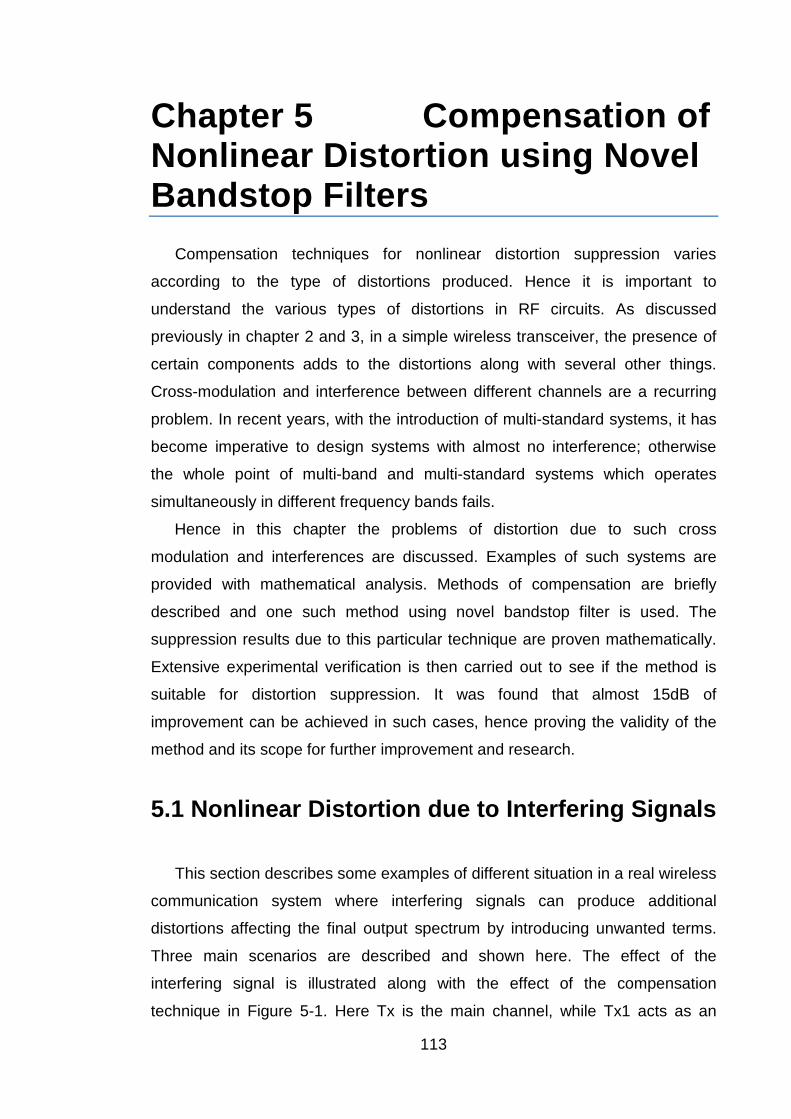
113
Chapter 5 Compensation of Nonlinear Distortion using Novel Bandstop Filters
Compensation techniques for nonlinear distortion suppression varies
according to the type of distortions produced. Hence it is important to
understand the various types of distortions in RF circuits. As discussed
previously in chapter 2 and 3, in a simple wireless transceiver, the presence of
certain components adds to the distortions along with several other things.
Cross-modulation and interference between different channels are a recurring
problem. In recent years, with the introduction of multi-standard systems, it has
become imperative to design systems with almost no interference; otherwise
the whole point of multi-band and multi-standard systems which operates
simultaneously in different frequency bands fails.
Hence in this chapter the problems of distortion due to such cross
modulation and interferences are discussed. Examples of such systems are
provided with mathematical analysis. Methods of compensation are briefly
described and one such method using novel bandstop filter is used. The
suppression results due to this particular technique are proven mathematically.
Extensive experimental verification is then carried out to see if the method is
suitable for distortion suppression. It was found that almost 15dB of
improvement can be achieved in such cases, hence proving the validity of the
method and its scope for further improvement and research.
5.1 Nonlinear Distortion due to Interfering Signals
This section describes some examples of different situation in a real wireless
communication system where interfering signals can produce additional
distortions affecting the final output spectrum by introducing unwanted terms.
Three main scenarios are described and shown here. The effect of the
interfering signal is illustrated along with the effect of the compensation
technique in Figure 5-1. Here Tx is the main channel, while Tx1 acts as an
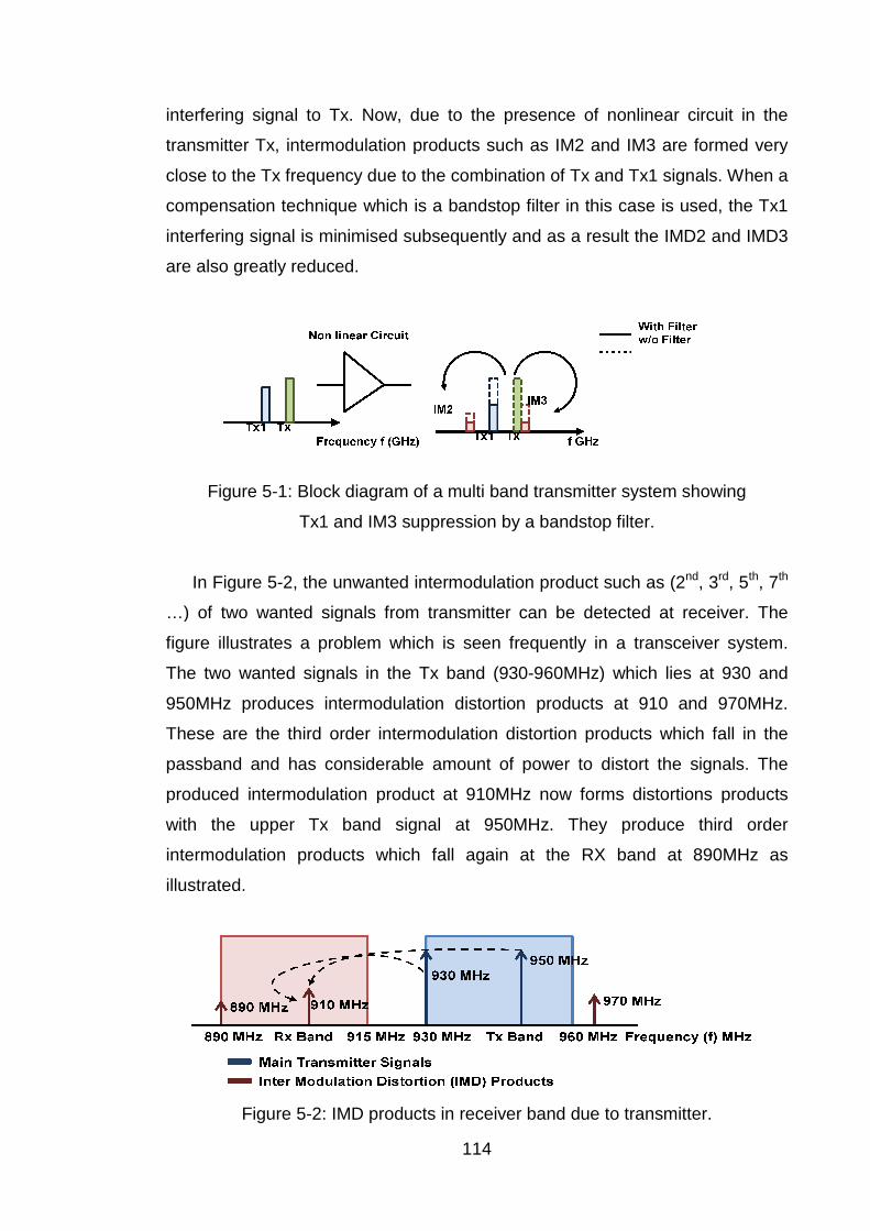
interfering signal to Tx.
transmitter Tx, intermodulation products such as IM2 and IM3 are formed very
close to the Tx frequency due to
compensation technique which is a bandstop
interfering signal is minimised subsequently and as a result the IMD2 and IMD3
are also greatly reduced.
Figure 5-1: Block d
Tx1 and IM3 suppression by
In Figure 5-2, the unwanted intermodulation product such as (2
…) of two wanted signals from transmitter can be detected at receiver. The
figure illustrates a problem which is seen frequently in a transceiver system.
The two wanted signals in the Tx band (930
950MHz produces intermodulation distortion products at 910 and 970
These are the third order
passband and has considerable amount of power to distort the signals. The
produced intermodulation product at 910
with the upper Tx band signal at 950
intermodulation products which fall again at the RX band at 890
illustrated.
Figure 5-2:
114
interfering signal to Tx. Now, due to the presence of nonlinear circuit in the
transmitter Tx, intermodulation products such as IM2 and IM3 are formed very
close to the Tx frequency due to the combination of Tx and Tx1 signals.
compensation technique which is a bandstop filter in this case is used
interfering signal is minimised subsequently and as a result the IMD2 and IMD3
greatly reduced.
1: Block diagram of a multi band transmitter system showing
Tx1 and IM3 suppression by a bandstop filter
the unwanted intermodulation product such as (2
…) of two wanted signals from transmitter can be detected at receiver. The
re illustrates a problem which is seen frequently in a transceiver system.
The two wanted signals in the Tx band (930-960MHz) which lies at 930 and
produces intermodulation distortion products at 910 and 970
These are the third order intermodulation distortion products which fall in the
passband and has considerable amount of power to distort the signals. The
produced intermodulation product at 910MHz now forms distortions products
Tx band signal at 950MHz. They produce
intermodulation products which fall again at the RX band at 890
2: IMD products in receiver band due to transmitter.
nonlinear circuit in the
transmitter Tx, intermodulation products such as IM2 and IM3 are formed very
the combination of Tx and Tx1 signals. When a
in this case is used, the Tx1
interfering signal is minimised subsequently and as a result the IMD2 and IMD3
iagram of a multi band transmitter system showing
filter.
the unwanted intermodulation product such as (2nd, 3rd, 5th, 7th
…) of two wanted signals from transmitter can be detected at receiver. The
re illustrates a problem which is seen frequently in a transceiver system.
) which lies at 930 and
produces intermodulation distortion products at 910 and 970MHz.
intermodulation distortion products which fall in the
passband and has considerable amount of power to distort the signals. The
now forms distortions products
. They produce third order
intermodulation products which fall again at the RX band at 890MHz as
products in receiver band due to transmitter.
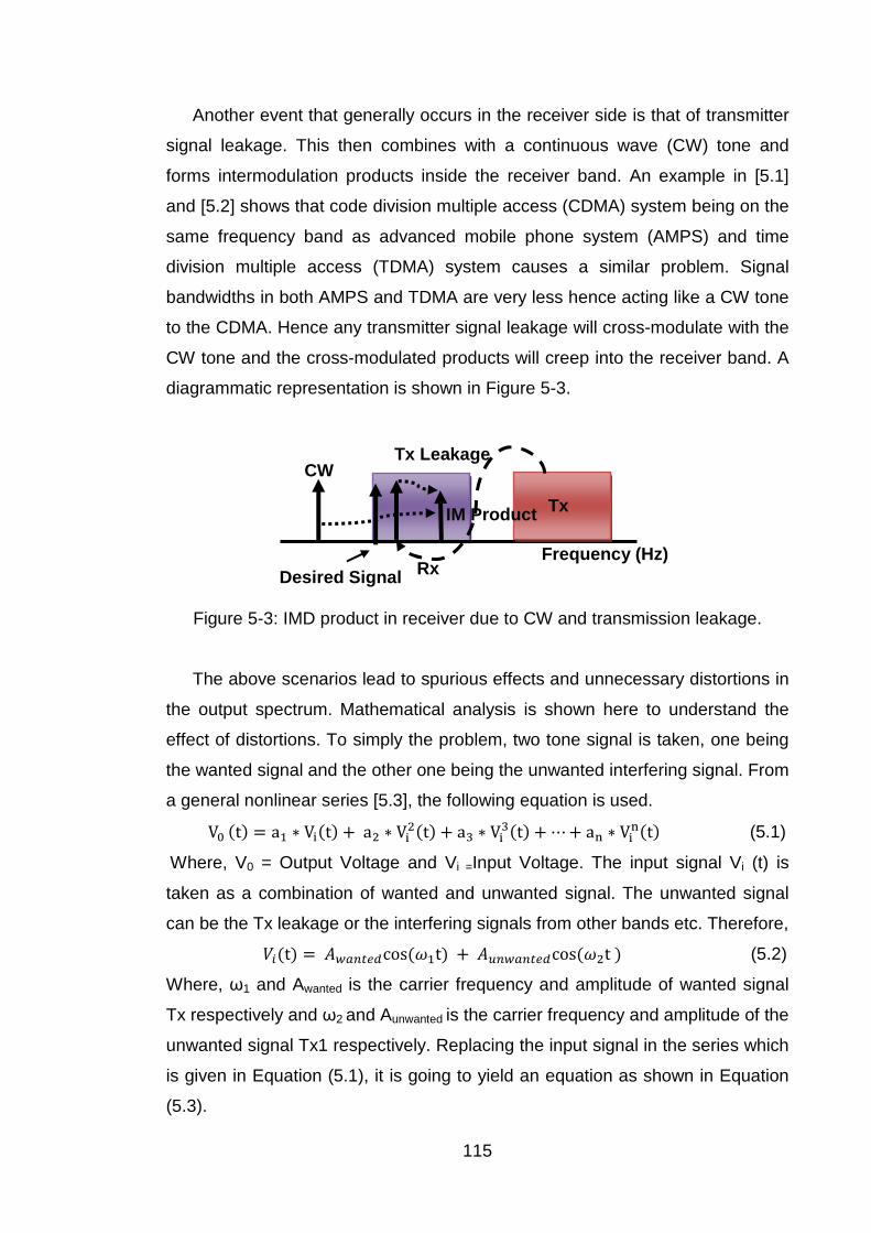
115
Another event that generally occurs in the receiver side is that of transmitter
signal leakage. This then combines with a continuous wave (CW) tone and
forms intermodulation products inside the receiver band. An example in [5.1]
and [5.2] shows that code division multiple access (CDMA) system being on the
same frequency band as advanced mobile phone system (AMPS) and time
division multiple access (TDMA) system causes a similar problem. Signal
bandwidths in both AMPS and TDMA are very less hence acting like a CW tone
to the CDMA. Hence any transmitter signal leakage will cross-modulate with the
CW tone and the cross-modulated products will creep into the receiver band. A
diagrammatic representation is shown in Figure 5-3.
Figure 5-3: IMD product in receiver due to CW and transmission leakage.
The above scenarios lead to spurious effects and unnecessary distortions in
the output spectrum. Mathematical analysis is shown here to understand the
effect of distortions. To simply the problem, two tone signal is taken, one being
the wanted signal and the other one being the unwanted interfering signal. From
a general nonlinear series [5.3], the following equation is used.
V t a Vt $ a& V&t $ a) V)t $ + $ aY VYt (5.1)
Where, V0 = Output Voltage and Vi =Input Voltage. The input signal Vi (t) is
taken as a combination of wanted and unwanted signal. The unwanted signal
can be the Tx leakage or the interfering signals from other bands etc. Therefore,
#t [,vcosIt $ u,[,vcosI&t (5.2)
Where, ω1 and Awanted is the carrier frequency and amplitude of wanted signal
Tx respectively and ω2 and Aunwanted is the carrier frequency and amplitude of the
unwanted signal Tx1 respectively. Replacing the input signal in the series which
is given in Equation (5.1), it is going to yield an equation as shown in Equation
(5.3).
Tx
Rx
Tx Leakage CW
IM Product
Frequency (Hz) Desired Signal
116
V t a WAY cos ωt $ AYY cos ω&tX $ a& WAY cos ωt $ AYY cos ω&tX& $ a) WAY cos ωt $ AYY cos ω&tX) $ + $ aY WAY cos ωt $ AYY cos ω&tXY (5.3)
In this case, the first three terms are the most important because of the fact
that these intermodulation products appear in the passband or in the vicinity of
the passband, the first three power term are evaluated separately for the ease
of calculation. The second term O& W[,v cos I $ u,[,v cos I&X& can be expanded using simple trigonometric equation where the
final result is as in Equation (5.5).
#& O& W[,v cos I $ u,[,v cos I&X& (5.4)
O& Za-(& $ D-a-(
& $ a-(& cos2I $ D-a-(
& cos2I&" $ cos I 1 I& $ cos I $ I&\ O& [,v& Z
& $ (& $
& cos2I $ (& cos2I&" $ cos I 1
I& $ cos I $ I&\ (5.5)
Where, D-a-a- , the ratio of the amplitudes of the unwanted and wanted
signal. Hence from this, the effect of the amplitude of the unwanted signal on
the 2nd order intermodulation products which occurs at ω1 - ω2 and ω1 + ω2 can
be seen. If the amplitude of the unwanted signal is zero, then β is zero. When
unwanted signal is high, β is also high. The value of β is greater than one when
the amplitude of the unwanted signal exceeds the amplitude of the wanted
signal. Now similarly evaluating the third term O& W[,v cos I $u,[,v cos I&X) the following results can be obtained as in Equation
(5.7) and (5.8).
#) O) Z)a-*^ $ )a- D-a-(
& cos I" $ )D-a-*^ $
)D-a- a-(& cos I&" $ a-*
^ cos 3I" $ D-a-*^
cos 3I&" $ )D-a- a-(^ cos 2I 1 I& $ cos 2I $
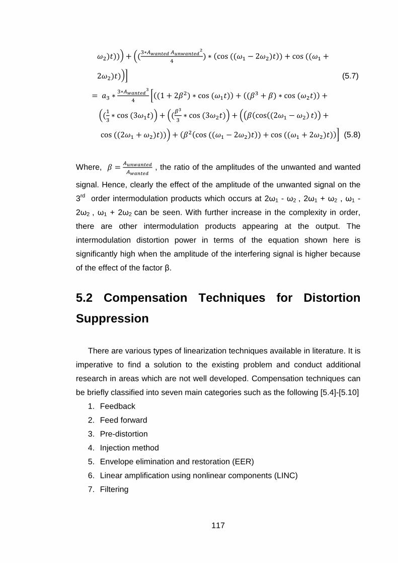
117
I&" $ )a- D-a-(^ cos I 1 2I& $ cos I $
2I&"\ (5.7)
O) )a-*^ Z1 $ 2& cos I $ ) $ cos I& $
) cos 3I" $ *
) cos 3I&" $ cos2I 1 I& $ cos 2I $ I&" $ &cos I 1 2I& $ cos I $ 2I&\ (5.8)
Where, D-a-a- , the ratio of the amplitudes of the unwanted and wanted
signal. Hence, clearly the effect of the amplitude of the unwanted signal on the
3rd order intermodulation products which occurs at 2ω1 - ω2 , 2ω1 + ω2 , ω1 -
2ω2 , ω1 + 2ω2 can be seen. With further increase in the complexity in order,
there are other intermodulation products appearing at the output. The
intermodulation distortion power in terms of the equation shown here is
significantly high when the amplitude of the interfering signal is higher because
of the effect of the factor β.
5.2 Compensation Techniques for Distortion
Suppression
There are various types of linearization techniques available in literature. It is
imperative to find a solution to the existing problem and conduct additional
research in areas which are not well developed. Compensation techniques can
be briefly classified into seven main categories such as the following [5.4]-[5.10]
1. Feedback
2. Feed forward
3. Pre-distortion
4. Injection method
5. Envelope elimination and restoration (EER)
6. Linear amplification using nonlinear components (LINC)
7. Filtering
118
The feedback linearization technique is a broader term for many different
types of feedback linearization such as RF feedback [5.11], modulation
feedback [5.12], polar loop [5.13] and Cartesian loop [5.14]. In its simplest form,
the feedback linearizer works by feeding back the distorted output signal which
is then passed through a voltage divider with a particular gain, the result from
this is then compared to the input signal forming the error signal. The main goal
is to correct the input signal as much as possible hence providing a linearized
output. The feedback system suffers from problems such as stability issues and
a reduction in the overall system gain. Several methods have been proposed in
order to get rid of it as in [5.15].
To do away with the disadvantages of the feedback method, feed forward
linearization technique is introduced. The fundamental concept of feed forward
lies in having two separate loops one for signal cancellation and the other for
error cancellation. The main input signal is passed through the nonlinear power
amplifier and is subtracted from a delayed version of itself, hence obtaining the
IMD products. These obtained distortion products are amplified to the required
level and then subtracted from the original signal thus obtaining a distortion free
linearized output signal. This takes place in the error loop [5.16]-[5.17]. The
problem with the feed forward system is the use of another Class A linear
amplifier, which sometimes can be high in cost and contribute to the overall
complexity of the system.
The concept of predistortion technique involves both analogue [5.18] and
digital [5.19] predistortions. The underlying concept lies in the introduction of a
previously inversed PA output which when combined with the real distorted
signal, gives a linearized output. The main difference between analogue and
digital predistortion technique lies in the fact that the former is used in the RF or
IF domain while the latter is used in the digital domain. While analogue
predistortion suffers from power loss due to additional RF components, digital
predistortion techniques can be extremely complex due to the lack of memory
effect consideration leading to an increase in circuit cost and size. In [5.20], an
adaptive digital predistortion technique is proposed with improved memory
effects.
Another common type of distortion suppression technique is the injection
method [5.21]-[5.23]. Injecting particular frequency components back into the
119
original circuit can cancel out the 3rd or 5th order harmonics according to the
components injected. This is mostly done with the frequency difference
component such as cosI 1 I& and the second harmonic component
cos 2I.These when mixed with the fundamental tone cos I , forms
additional third order intermodulation products at cos2I 1 I& This can be
then amplitude and phase adjusted to cancel out the third order distortion
product already produced. Hence a linear output can be achieved. The major
drawback of such techniques is the inability of the phase and the gain to be
accurately adjusted leading to further problems. Additional low amplitude
distortion products formed can also distort the output signal in some cases.
The envelope elimination and restoration method [5.24] comprises of the
input signal being divided into two parts, one of which is passed through an
envelope detector forming the AM part and the other a limiter, forming the PM
part. The AM part is subsequently amplified by a baseband amplifier while the
PM part is amplified by a RF amplifier. The final envelope restoration happens
when the AM signal is used to modulate the final RF signal. The limiter helps in
getting rid of the AM/PM distortions and hence a linearized output is obtained.
Few possible disadvantages of the EER method are nonlinearity of the
baseband amplifier, envelope detector etc., and delays in the path and reduced
efficiency of the system [5.25].
Another linearizer concept is the linear amplification using nonlinear
components [5.26]-[5.27]. This type of linearizer uses nonlinear components to
achieve a linear output. The main task involved is to split the incoming signal
into two parts of phase modulated signal having constant envelopes using an
AM-PM modulator. Each individual part is then amplified using highly efficient
power amplifiers, and added at the output. This signal has a linear relationship
with the input signal thus eliminating distortions and giving a linearized effect.
There are many drawbacks of this system including complexity, realization of a
AM-PM modulator and phase and gain imbalance of the two branches using
identical power amplifiers [5.28]-[5.29].
The filtering concept has been explained in [5.30] and [5.31] where filtering
is used both before and after the power amplifier in order to get rid of
distortions. Filtering can be done either by a bandpass filter or a bandstop filter.
120
The BPF has resonators which resonate in the passband. These can however
induce transmission loss due to the resistance of the resonators. A steep phase
change response is seen due to resonance which can also contribute to the
loss. On the other hand, the BSF has resonators which resonate in the stop
band. These have lower transmission loss and variation in group delay as
compared to BPF. In cases where a BSF is used after the power amplifier, a
dual-band filter is required in order to filter out both sides of distortions. Such
filters needs to be designed with the power requirements in mind. In cases
where interfering signals are present, these can further contribute to nonlinearity
as mathematically shown in the next section. Such cases require inter-stage
bandstop filters as in [5.2].
5.3 Mathematical Analysis showing Interference
Suppression using Novel Bandstop Filter
As previously mentioned in Section 5.2, using a bandstop filter for distortion
suppression due to interfering signals is the most convenient method in terms of
implementation, size and cost. In order to have an initial proof of theory
mathematical expressions were derived which showed that filters could be a
possible way of interference reduction and hence an overall reduction in
distortions in the output spectrum can be achieved. This will be proved in this
section and in the next. This section mostly deals with the proof of theory and
mathematical derivations along with both simulation and experimental
verification using a nonlinear power amplifier as DUT.
The proposed method shown has been developed and tested using a PA as
the DUT. Operating the power amplifier in the saturation region has become
vital with the onset of 4G LTE systems which provides excellent data rates and
faster communication. This will result in higher efficiency for the amplifier but
with reduced linearity. Correction of such IMD products in wireless transmitters
is therefore a necessity [5.20].
High power interfering signal along with the main signal can make the
intermodulation distortion much worse and can distort the output spectrum
considerably. Different methods of PA linearization can be used to overcome
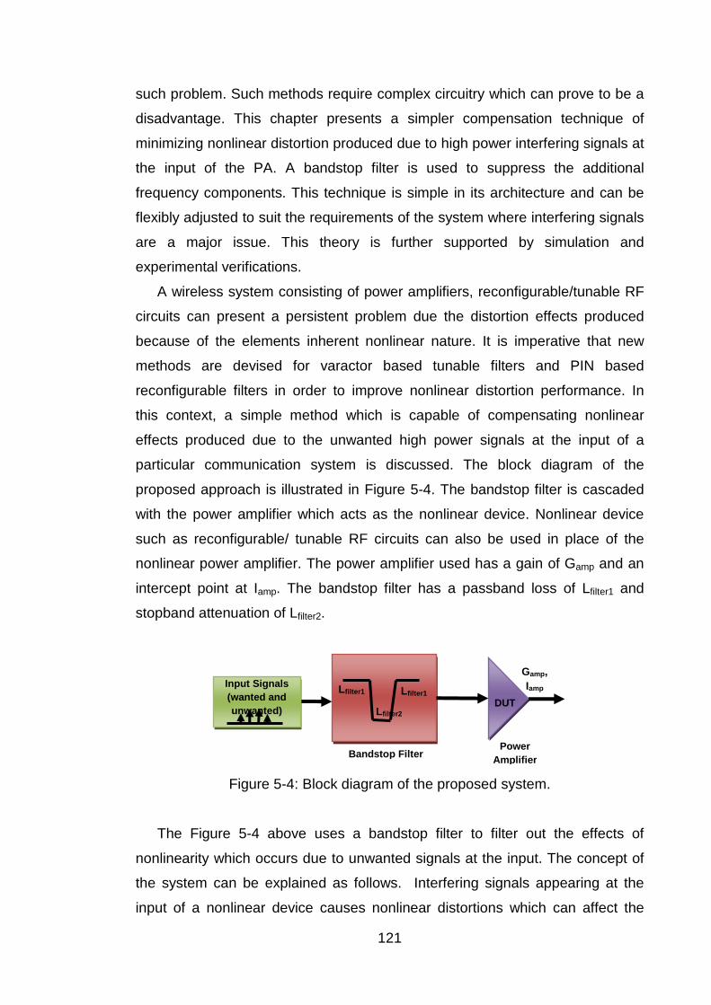
121
such problem. Such methods require complex circuitry which can prove to be a
disadvantage. This chapter presents a simpler compensation technique of
minimizing nonlinear distortion produced due to high power interfering signals at
the input of the PA. A bandstop filter is used to suppress the additional
frequency components. This technique is simple in its architecture and can be
flexibly adjusted to suit the requirements of the system where interfering signals
are a major issue. This theory is further supported by simulation and
experimental verifications.
A wireless system consisting of power amplifiers, reconfigurable/tunable RF
circuits can present a persistent problem due the distortion effects produced
because of the elements inherent nonlinear nature. It is imperative that new
methods are devised for varactor based tunable filters and PIN based
reconfigurable filters in order to improve nonlinear distortion performance. In
this context, a simple method which is capable of compensating nonlinear
effects produced due to the unwanted high power signals at the input of a
particular communication system is discussed. The block diagram of the
proposed approach is illustrated in Figure 5-4. The bandstop filter is cascaded
with the power amplifier which acts as the nonlinear device. Nonlinear device
such as reconfigurable/ tunable RF circuits can also be used in place of the
nonlinear power amplifier. The power amplifier used has a gain of Gamp and an
intercept point at Iamp. The bandstop filter has a passband loss of Lfilter1 and
stopband attenuation of Lfilter2.
Figure 5-4: Block diagram of the proposed system.
The Figure 5-4 above uses a bandstop filter to filter out the effects of
nonlinearity which occurs due to unwanted signals at the input. The concept of
the system can be explained as follows. Interfering signals appearing at the
input of a nonlinear device causes nonlinear distortions which can affect the
Power Amplifier Bandstop Filter
Gamp, Iamp Lfilter1
Lfilter2
Lfilter1 Input Signals (wanted and unwanted)
DUT
122
clarity of the output signal. Thus when a bandstop filter designed at the same
centre frequency as the unwanted signals is used; the distortions can be filtered
out. The stopband attenuation of the designed filter will determine the amount
by which the IMD distortions get reduced [5.31]. To calculate the nonlinear
distortion of the nonlinear device, such as a power amplifier in this case, the
block diagram in Figure 5-4 can be used, which shows a bandstop filter with
Lfilter2 as the stopband attenuation and Lfilter1 as the passband attenuation, the
power amplifier has a gain Gamp1 and third order intercept (TOI) point Iamp1.
The interfering signals of power level Pin dBm combines with the wanted
signals producing intermodulation components as the system has nonlinear
blocks. Due to the placement of the bandstop filter where the interfering signals
falls in the stopband and the input signal (wanted signal) is assumed to be in
the passband of the system, the distortions are greatly reduced. The output
power level of the IMD signals at the output is calculated for both cases. The
case to be considered is when no bandstop filter is used. Nonlinear distortion
products produced due to the amplifier will have an output power level as
follows:
.@/ 3 .#, 1 2 3[ $ [ 1 #yv¡ (5.9)
Where, Pw/o = 3rd order IMD power without bandstop filter, Pin = unwanted input
signal power, Iamp1 = 3rd order intercept point and Lfilter1 = passband attenuation
of the bandstop filter which is negligible, Gamp1 = gain of PA. Similarly the case
where bandstop filter is used can be now considered. The equation (5.10)
shows the power level of the IMD when filter is used. This is now expanded to
give equation (5.11).
./#yv¡ 3 .#, 1 #yv¡& 1 2 3[ $ [ (5.10)
./#yv¡ 3 .#, 1 2 3[ $ [ 1 3 #yv¡& (5.11)
Where, Pw/filter = 3rd order IMD power after using filter, Pin = unwanted input
signal power, Iamp1 = 3rd order intercept point and Lfilter2 = stopband attenuation
of the bandstop filter, Gamp1 = gain of PA.
When the above results are compared , it is clearly seen from equation (5.9)
and equation (5.11) that for the reduction of third order intermodulation power,
the bandstop filter plays a major role. The two expressions can be written in
terms of each other as in equation (5.12).
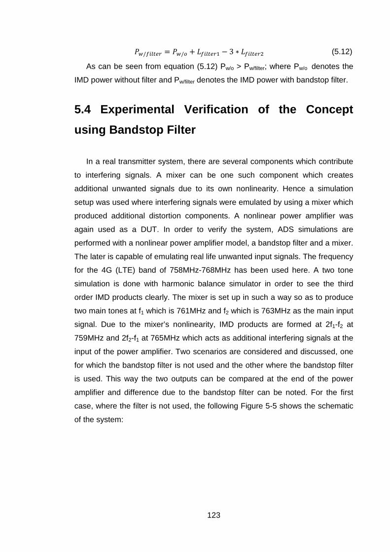
123
./#yv¡ ./ $ #yv¡ 1 3 #yv¡& (5.12)
As can be seen from equation (5.12) Pw/o > Pw/filter; where Pw/o denotes the
IMD power without filter and Pw/filter denotes the IMD power with bandstop filter.
5.4 Experimental Verification of the Concept
using Bandstop Filter
In a real transmitter system, there are several components which contribute
to interfering signals. A mixer can be one such component which creates
additional unwanted signals due to its own nonlinearity. Hence a simulation
setup was used where interfering signals were emulated by using a mixer which
produced additional distortion components. A nonlinear power amplifier was
again used as a DUT. In order to verify the system, ADS simulations are
performed with a nonlinear power amplifier model, a bandstop filter and a mixer.
The later is capable of emulating real life unwanted input signals. The frequency
for the 4G (LTE) band of 758MHz-768MHz has been used here. A two tone
simulation is done with harmonic balance simulator in order to see the third
order IMD products clearly. The mixer is set up in such a way so as to produce
two main tones at f1 which is 761MHz and f2 which is 763MHz as the main input
signal. Due to the mixer’s nonlinearity, IMD products are formed at 2f1-f2 at
759MHz and 2f2-f1 at 765MHz which acts as additional interfering signals at the
input of the power amplifier. Two scenarios are considered and discussed, one
for which the bandstop filter is not used and the other where the bandstop filter
is used. This way the two outputs can be compared at the end of the power
amplifier and difference due to the bandstop filter can be noted. For the first
case, where the filter is not used, the following Figure 5-5 shows the schematic
of the system:
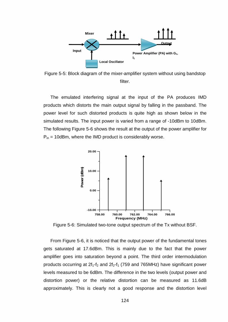
124
Figure 5-5: Block diagram of the mixer-amplifier system without using bandstop
filter.
The emulated interfering signal at the input of the PA produces IMD
products which distorts the main output signal by falling in the passband. The
power level for such distorted products is quite high as shown below in the
simulated results. The input power is varied from a range of -10dBm to 10dBm.
The following Figure 5-6 shows the result at the output of the power amplifier for
Pin = 10dBm, where the IMD product is considerably worse.
Figure 5-6: Simulated two-tone output spectrum of the Tx without BSF.
From Figure 5-6, it is noticed that the output power of the fundamental tones
gets saturated at 17.6dBm. This is mainly due to the fact that the power
amplifier goes into saturation beyond a point. The third order intermodulation
products occurring at 2f1-f2 and 2f2-f1 (759 and 765MHz) have significant power
levels measured to be 6dBm. The difference in the two levels (output power and
distortion power) or the relative distortion can be measured as 11.6dB
approximately. This is clearly not a good response and the distortion level
758.00 760.00 762.00 764.00 766.00
-10.00
0.00
10.00
20.00
Frequency (MHz)
Pow
er (dB
m)
Mixer
Power Amplifier (PA) with G 1, I1
Local Oscillator
Output Input

125
needs to be further improved. Hence in the next simulated case, a bandstop
filter with centre frequency same as the interfering tones are used, which in this
case are 759MHz and 765MHz.
The utility of the inter-stage bandstop filter lies in the fact that it can block
unnecessary signals which in turn can minimise the IMD product to a large
extent. This particular example case requires a dual-band bandstop filter due to
the appearance of multiple unwanted signals. The centre frequencies of both
bands are chosen so as to attenuate the unwanted signals falling in the
stopband. The stopband attenuation is chosen to be 30dB. The following shows
the response of the bandstop filter block used. It has two bands with centre
frequencies located at 753MHz and 771MHz. The choice of centre frequency is
critical as it has the capability to minimise other interfering signals that may
occur in that particular band.
Figure 5-7: Simulated S-parameters of the bandstop filter.
From Figure 5-7, it is clear that the characteristics of the dual-band bandstop
filter are critical. Here a narrow bandwidth (approximately 30MHz) is used in
order to minimise distortions. The solid line represents the S21 response, while
the dotted line shows the S11 response of the filter. From equation (5.12)
above, the power of the intermodulation distortion product will be considerably
reduced when the interferers fall in the stopband of the filter. The main signal at
the input of the power amplifier passes unscathed due to its placement in the
passband of the filter. Figure 5-8 shows the simulation setup used.
700.00 720.00 740.00 760.00 780.00 800.00
-80.00
-60.00
-40.00
-20.00
0.00
S-p
aram
eter
(dB
)
Frequency (MHz)
S11
S21
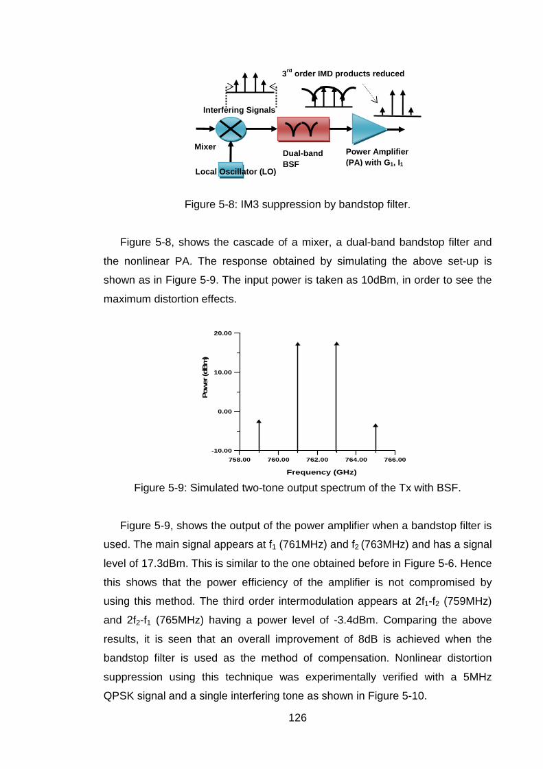
126
Figure 5-8: IM3 suppression by bandstop filter.
Figure 5-8, shows the cascade of a mixer, a dual-band bandstop filter and
the nonlinear PA. The response obtained by simulating the above set-up is
shown as in Figure 5-9. The input power is taken as 10dBm, in order to see the
maximum distortion effects.
Figure 5-9: Simulated two-tone output spectrum of the Tx with BSF.
Figure 5-9, shows the output of the power amplifier when a bandstop filter is
used. The main signal appears at f1 (761MHz) and f2 (763MHz) and has a signal
level of 17.3dBm. This is similar to the one obtained before in Figure 5-6. Hence
this shows that the power efficiency of the amplifier is not compromised by
using this method. The third order intermodulation appears at 2f1-f2 (759MHz)
and 2f2-f1 (765MHz) having a power level of -3.4dBm. Comparing the above
results, it is seen that an overall improvement of 8dB is achieved when the
bandstop filter is used as the method of compensation. Nonlinear distortion
suppression using this technique was experimentally verified with a 5MHz
QPSK signal and a single interfering tone as shown in Figure 5-10.
758.00 760.00 762.00 764.00 766.00
-10.00
0.00
10.00
20.00
Pow
er (dB
m)
Frequency (GHz)
Mixer
3rd order IMD products reduced
Dual -band BSF
Interfering Signals
Power Amplifier (PA) with G 1, I1
Local Oscillator (LO)
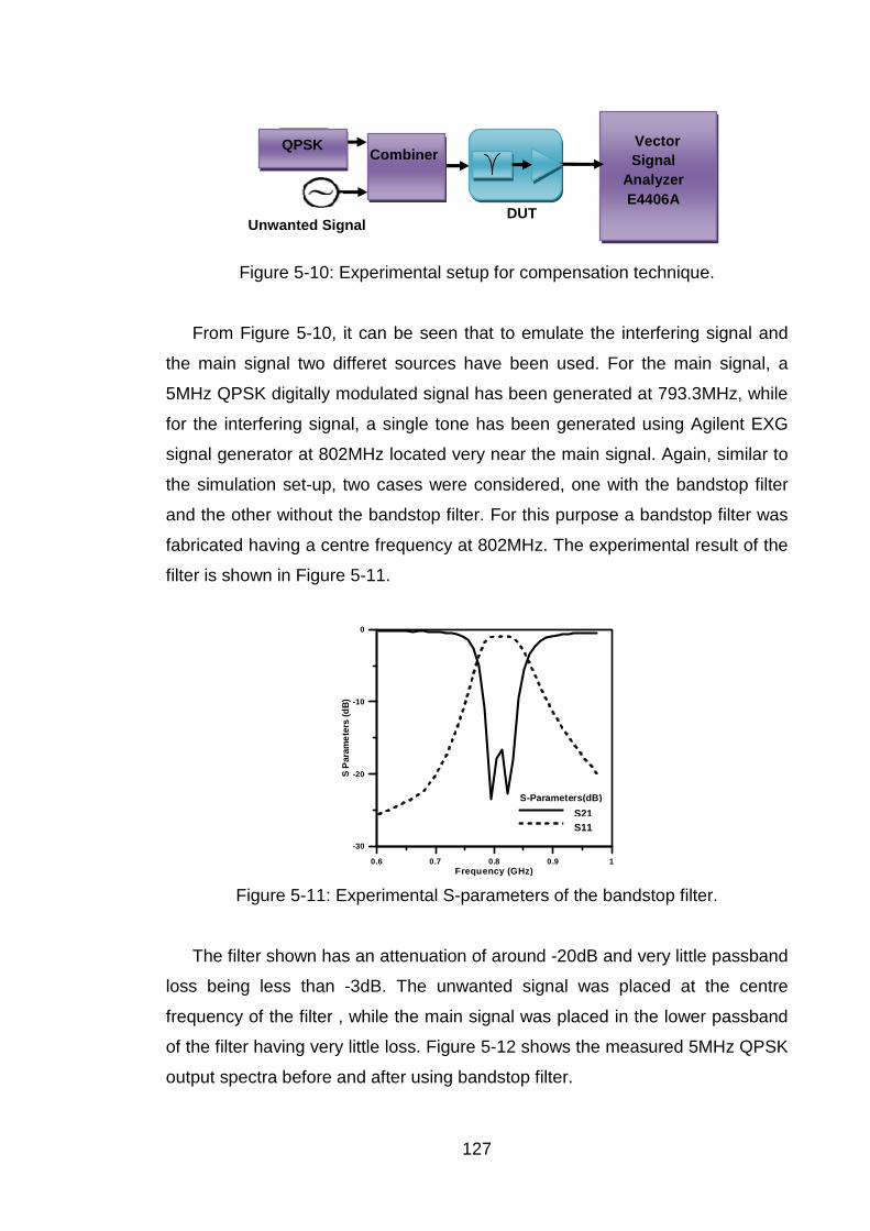
127
Figure 5-10: Experimental setup for compensation technique.
From Figure 5-10, it can be seen that to emulate the interfering signal and
the main signal two differet sources have been used. For the main signal, a
5MHz QPSK digitally modulated signal has been generated at 793.3MHz, while
for the interfering signal, a single tone has been generated using Agilent EXG
signal generator at 802MHz located very near the main signal. Again, similar to
the simulation set-up, two cases were considered, one with the bandstop filter
and the other without the bandstop filter. For this purpose a bandstop filter was
fabricated having a centre frequency at 802MHz. The experimental result of the
filter is shown in Figure 5-11.
0.6 0.7 0.8 0.9 1Frequency (GHz)
-30
-20
-10
0
SP
aram
ete
rs(d
B)
S-Parameters(dB)S11S21
Figure 5-11: Experimental S-parameters of the bandstop filter.
The filter shown has an attenuation of around -20dB and very little passband
loss being less than -3dB. The unwanted signal was placed at the centre
frequency of the filter , while the main signal was placed in the lower passband
of the filter having very little loss. Figure 5-12 shows the measured 5MHz QPSK
output spectra before and after using bandstop filter.
DUT
QPSK Combiner
Unwanted Signal
Vector Signal
Analyzer E4406A
S21 S11
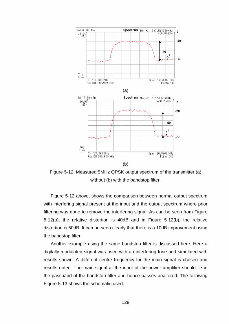
128
(a)
(b)
Figure 5-12: Measured 5MHz QPSK output spectrum of the transmitter (a)
without (b) with the bandstop filter.
Figure 5-12 above, shows the comparison between normal output spectrum
with interfering signal present at the input and the output spectrum where prior
filtering was done to remove the interfering signal. As can be seen from Figure
5-12(a), the relative distortion is 40dB and in Figure 5-12(b), the relative
distortion is 50dB. It can be seen clearly that there is a 10dB improvement using
the bandstop filter.
Another example using the same bandstop filter is discussed here. Here a
digitally modulated signal was used with an interfering tone and simulated with
results shown. A different centre frequency for the main signal is chosen and
results noted. The main signal at the input of the power amplifier should lie in
the passband of the bandstop filter and hence passes unaltered. The following
Figure 5-13 shows the schematic used.
40
0
-60
50
0
-70
-20
-20
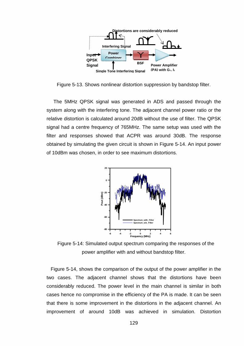
129
Figure 5-13. Shows nonlinear distortion suppression by bandstop filter.
The 5MHz QPSK signal was generated in ADS and passed through the
system along with the interfering tone. The adjacent channel power ratio or the
relative distortion is calculated around 20dB without the use of filter. The QPSK
signal had a centre frequency of 765MHz. The same setup was used with the
filter and responses showed that ACPR was around 30dB. The response
obtained by simulating the given circuit is shown in Figure 5-14. An input power
of 10dBm was chosen, in order to see maximum distortions.
-6 -4 -2 0 2 4 6Frequency (MHz)
-80
-60
-40
-20
0
20
Pou
t(dB
m)
Spectrum_with_FilterSpectrum_w/o_Filter
Figure 5-14: Simulated output spectrum comparing the responses of the
power amplifier with and without bandstop filter.
Figure 5-14, shows the comparison of the output of the power amplifier in the
two cases. The adjacent channel shows that the distortions have been
considerably reduced. The power level in the main channel is similar in both
cases hence no compromise in the efficiency of the PA is made. It can be seen
that there is some improvement in the distortions in the adjacent channel. An
improvement of around 10dB was achieved in simulation. Distortion
Power Combiner
BSF
Interfering Signal
Single Tone Interfering Signal
Power Amplifier (PA) with G 1, I1
Input QPSK Signal
Distortions are considerably reduced
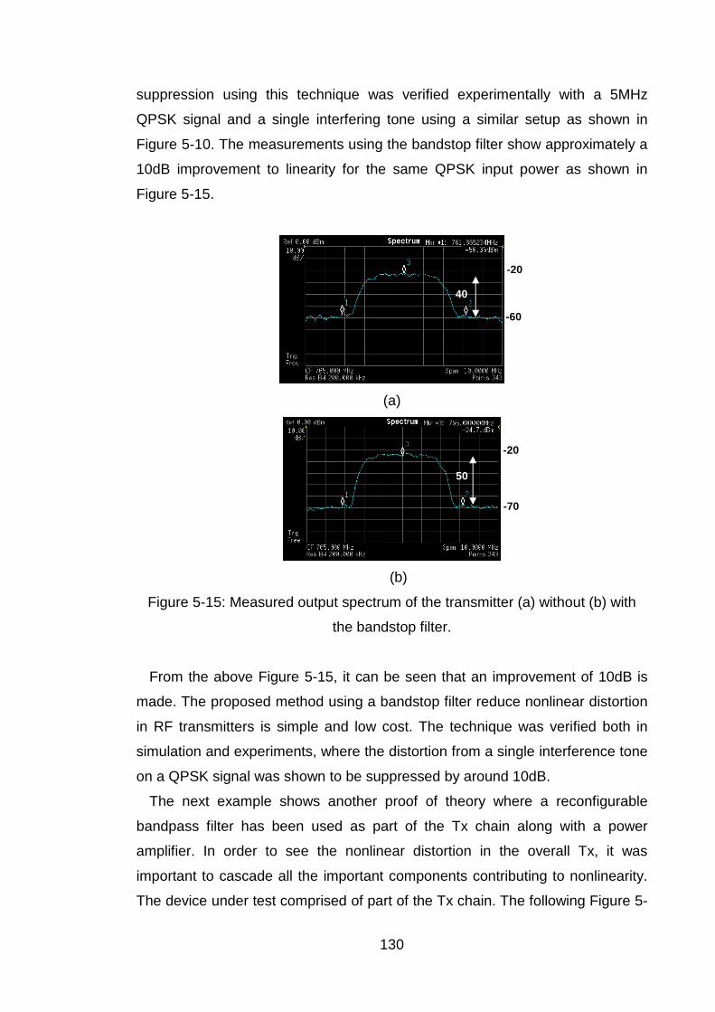
130
suppression using this technique was verified experimentally with a 5MHz
QPSK signal and a single interfering tone using a similar setup as shown in
Figure 5-10. The measurements using the bandstop filter show approximately a
10dB improvement to linearity for the same QPSK input power as shown in
Figure 5-15.
(a)
(b)
Figure 5-15: Measured output spectrum of the transmitter (a) without (b) with
the bandstop filter.
From the above Figure 5-15, it can be seen that an improvement of 10dB is
made. The proposed method using a bandstop filter reduce nonlinear distortion
in RF transmitters is simple and low cost. The technique was verified both in
simulation and experiments, where the distortion from a single interference tone
on a QPSK signal was shown to be suppressed by around 10dB.
The next example shows another proof of theory where a reconfigurable
bandpass filter has been used as part of the Tx chain along with a power
amplifier. In order to see the nonlinear distortion in the overall Tx, it was
important to cascade all the important components contributing to nonlinearity.
The device under test comprised of part of the Tx chain. The following Figure 5-
40
-60
-20
-20
-70
50

131
16 shows the setup used where a 5MHz QPSK signal at a center frequency of
2.14GHz was used as the main input signal. The interference tone was located
at 2.28GHz. The signals were generated separately and combined with a power
combiner. The power amplifier had a gain of 10dB. Hence when interfering
signals are present, due to amplification in subsequent stages, the effect of a
very strong interfering signal is seen, while in the case where interfering signal
is already attenuated by the BSF, very little effect is seen as discussed below.
Figure 5-16: Experimental set-up for Tx interference suppresion.
The interfering signal power was hence 20dBm after the amplifier stage.
Hence a relative distortion of around 35dB is noticed with the case when no
bandstop filter is used. The adjacent channel shows the effect of the strong
interfering signal as shown in Figure 5-17. The bandstop filter has a center
frequency of 2.28GHz and has a filter response as shown in chapter 4, Figure
4-25. The 5MHz QPSK output spectrum shown for the case where bandstop
filter is used has a much better response with a relative distortion of around
51dB. It was noticed that the output power level of the main channel remains
the same for both cases with no effect in efficiency of the Tx system. Figure 5-
17 below shows the output spectrum for both cases with and without filter.
(a)
QPSK Power
Combiner
Signal Generator A
Agilent Vector Signal Analyser
E4406A
DUT
35dB
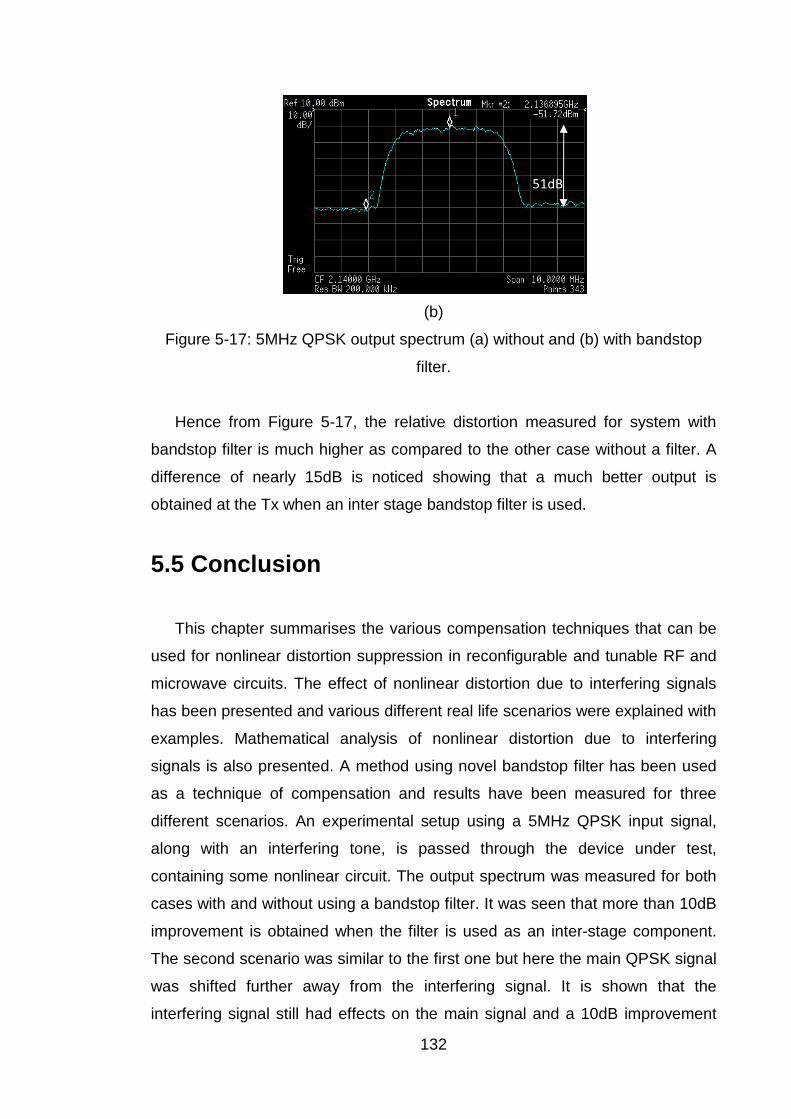
132
(b)
Figure 5-17: 5MHz QPSK output spectrum (a) without and (b) with bandstop
filter.
Hence from Figure 5-17, the relative distortion measured for system with
bandstop filter is much higher as compared to the other case without a filter. A
difference of nearly 15dB is noticed showing that a much better output is
obtained at the Tx when an inter stage bandstop filter is used.
5.5 Conclusion
This chapter summarises the various compensation techniques that can be
used for nonlinear distortion suppression in reconfigurable and tunable RF and
microwave circuits. The effect of nonlinear distortion due to interfering signals
has been presented and various different real life scenarios were explained with
examples. Mathematical analysis of nonlinear distortion due to interfering
signals is also presented. A method using novel bandstop filter has been used
as a technique of compensation and results have been measured for three
different scenarios. An experimental setup using a 5MHz QPSK input signal,
along with an interfering tone, is passed through the device under test,
containing some nonlinear circuit. The output spectrum was measured for both
cases with and without using a bandstop filter. It was seen that more than 10dB
improvement is obtained when the filter is used as an inter-stage component.
The second scenario was similar to the first one but here the main QPSK signal
was shifted further away from the interfering signal. It is shown that the
interfering signal still had effects on the main signal and a 10dB improvement
51dB
133
was achieved using a bandstop filter. The third scenario tested a combination of
a reconfigurable bandpass filter along with power amplifier forming part of the
Transmitter system. It was seen that a 15dB improvement was achieved using
an inter-stage bandstop filter. This technique of nonlinear distortion
compensation shows a good suppression till 15dB. It is superior to other such
methods available in literature in terms of cost as very inexpensive microstrip
bandstop filters can be designed. This method can directly be used in the RF
section of the transceiver without the need of any digital signal processing. This
in term reduces complexity and makes the process much simpler.
134
5.6 References [5.1] Q. Gu, RF System Design of Transceivers for Wireless Communications,
Springer USA, 2005.
[5.2] T. Ito, M. Kanemaru and A. Matsuzawa, “A 0.8-1.5GHz Multi-Standard
WCDMA Receiver with an Inter-Stage Tunable Notch Filter”, European
Microwave Conference, France, Sept 2010, pp. 1118-1121.
[5.3] W. Eberle, “Wireless Transceiver Systems Design" Springer USA, 2008
[5.4] A. F. Mitchell, “A 135MHz feedback amplifier,” IEE Colloq. Broadband High
Frequency Amplifiers: Practice and Theory, pp. 2/1-2/6, London, Nov. 1979.
[5.5] Y. Yang, and B. Kim, “A new linear amplifier using low-frequency second-
order intermodulation component feedforwarding,” IEEE Microwave and Guided
Wave Letters, vol. 9, no. 10, pp. 419–421, Oct. 1999.
[5.6] S. Chung, J. W. Holloway, and J. L. Dawson, “Energy-efficient digital
predistortion with lookup table training using analog cartesian feedback,” IEEE
Transactions on Microwave Theory Tech. vol. 56, no. 10, pp. 385-392, Oct.
2008.
[5.7] C. S. Aitchison, M. Mbabele, M. R. Moazzam., D. Budimir, and F. Ali,
“Improvement of third order intermodulation products of RF and microwave
amplifiers by injection," IEEE Transactions on Microwave Theory and
Techniques, vol. 49, no. 6, pp. 1148-1154, June 2001.
[5.8] F. H. Raab, “Envelope-elimination-and-restoration system concepts,” In
Proc. 1987-RF Expo East, Boston, MA, pp. 167 - 177, Nov. 1987.
[5.9] D.C. Cox, “Linear amplification with nonlinear components”, IEEE
Transactions on Communication Technology, vol. 22, no 12, pp 1942-1945,
Dec. 1974.
[5.10] C. Rauscher, "Varactor-tuned active notch filter with low passband noise
and signal distortion," Microwave Theory and Techniques, IEEE Transactions
on, vol.49, no.8, pp.1431-1437, Aug 2001.
[5.11] A. F. Mitchell, “A 135MHz feedback amplifier,” IEE Colloq. Broadband
High Frequency Amplifiers: Practice and Theory, pp. 2/1-2/6, London, Nov.
1979.
[5.12] T. Arthanayake, and H. B. Wood, “Linear amplification using envelope
feedback,” IEE Electronics Letters, vol. 7, no. 7, pp. 145-146, Apr. 1971.
135
[5.13] V. Petrovic, and W. Gosling, “Polar-loop transmitter”, IEE Electronics
Letters, vol. 15, no. 10, pp. 286-288, May 1979.
[5.14] M. Johansson, and L. Sundstrom, “Linearization of RF multicarrier
amplifiers using Cartesian feedback,” IEE Electronics Letters, vol. 30, no. 14,
pp. 1110-1111, Jul. 1994.
[5.15] M. Faulkner, “Amplifier linearization using RF feedback and feedforward
techniques,” IEEE Transactions on Vehicular Technology, vol. 47, pp. 209-215,
Feb., 1998.
[5.16] Y. K. G. Hau, V. Postoyalko, and J. R. Richardson, “Design and
characterization of a microwave feed-forward amplifier with improved wide-band
distortion cancellation,” IEEE Transactions on Microwave Theory Tech. vol. 49,
no. 1, pp. 200-203, Jan. 2001.
[5.17] S. P. Stapleton, “Adaptive feedforward linearization for RF power
amplifiers,” 55th ARFTG Conference Digest-Spring, vol. 37, pp. 1-7, Jun. 2000.
[5.18] W. Huang, R.E. Sand, "Novel third-order distortion generator with residual
IM2 suppression capabilities," IEEE Transactions on Microwave Theory and
Techniques, vol.46, no.12, pp.2372-2382, Dec 1998.
[5.19] S. Chung, J. W. Holloway, and J. L. Dawson, “Open-loop digital
predistortion using Cartesian feedback for adaptive RF power amplifier
linearization,” in Proc. IEEE MTT-S Int. Microw. Symp. Dig., Jun. 2007, pp.
1449–1452.
[5.20] D. Bondar, and D. Budimir, “Digital baseband predistortion of wideband
power amplifiers with improved memory effects,” in Proc. IEEE Radio and
Wireless Symposium, Jan. 2009, pp. 284-287.
[5.21] N. Males-Ilic, B. Milovanovic, and D. Budimir, “Improvement in second
harmonics linearization technique for multichannel amplifiers,” Microwave and
Optical Technology Letters, vol.38, no. 2, pp. 150-153, Jul. 2003.
[5.22] M. R. Moazzam, C. S. Aitchison, “A low third order intermodulation
amplifier with harmonic feedback circuitry,” IEEE MTT-S Int. Microwave Symp.
Dig., vol.2, pp.827-830, 1996.
[5.23] M. Modeste, et al., “Analysis and Practical Performance of Difference
Frequency Technique for Improving the Multicarrier IMD Performance of RF
Amplifiers,” IEEE MTT Symposium on Technologies for Wireless Applications,
Vancouver, pp.53-56, Feb. 1999.
136
[5.24] L. R. Kahn, “Single sideband transmission by envelope elimination and
restoration,” Proc. of the Institute of Radio Engineers, vol.40 no.7, pp.803-806,
Jul. 1952.
[5.25] F. H. Raab,”Envelope-elimination-and-restoration system concepts,” In
Proc. 1987-RF Expo East, Boston, MA, pp. 167 - 177, Nov. 1987.
[5.26] D.C. Cox, “Linear amplification with nonlinear components”, IEEE
Transactions on Communication Technology, vol. 22, no 12, pp 1942-1945,
Dec. 1974.
[5.27] X. Zhang, L. E. Larson, “Gain and phase error-free LINC transmitter,”
IEEE Transactions on Vehicular Technology, vol. 49, no. 5, pp. 1986-1994,
Sept. 2000.
[5.28] F. J. Casadevall, and A. Valdorinos, “Performance analysis of QAM
modulations applied to the LINC transmitter,” IEEE Trans. Veh. Technol., vol.
42, no. 4, pp. 399-406, Nov. 1993.
[5.29] A. Grebennikov, “RF and Microwave Transmitter Design”, John Wiley &
Sons, Inc., 2011.
[5.30] H. Uchida, H. Kamino, K. Totani, N. Yoneda , M. Miyazaki, Y. Konishi, S.
Makino, J. Hirokawa, M. Ando, "Dual-band-rejection filter for distortion reduction
in RF transmitters," Microwave Theory and Techniques, IEEE Transactions on ,
vol.52, no.11, pp.2550,2556, Nov. 2004.
[5.31] J.D. Rhodes and I.C. Hunter, “Synthesis of reflection-mode prototype
networks with dissipative circuit elements” IEE Proc. Microwave Antenna
Propagation, Vol.144, No.6 December 1997, pp.437-442.
137
Chapter 6 Conclusion
This chapter summarises some of the main concepts of this thesis including
a recap of the work done, original contributions made and potential future works
that can be carried out. The most important part of this thesis is to develop
novel bandstop filters for the use in distortion compensation in RF circuits due
to the presence of strong interfering signals in multi-standard wireless system.
Prior to that, RF circuits showing nonlinear property was experimentally verified
for nonlinear distortion effects using advanced digitally modulated signals.
The thesis aims to address some gaps in research such as the evaluation of
nonlinear distortions in RF circuits which includes reconfigurable/tunable filters
using digitally modulated signal , creating new tunable bandstop filter using
defected microstrip structure, which produces extremely miniaturized circuits
due to the inherent properties. A detailed literature review was provided to see
these gaps more clearly and problems that needed to be rectified.
A major part of the thesis was to evaluate nonlinear distortions in PIN
diodes, varactor diodes and optical switches and filters which use these
elements for reconfigurability and tunability. These elements contain inherent
nonlinear properties and the amount of nonlinear distortion needs to be
tabulated using real life signals. An experimental setup was created where
these circuits were used as device under test to test for nonlinearity. Among the
digitally modulated signals QPSK, 16 QAM, 64 QAM, 16QAM OFDM and 64
QAM OFDM are extensively used as 3G and 4G signals to give a complete
picture of nonlinear distortion measure for PIN diodes, optical switches and
reconfigurable filters using PIN diodes and optical switches as reconfigurable
elements.
The second most important part of the thesis deals with the development of
RF bandstop filters using defected microstrip structure. These can be divided
into two parts .The first part deals with the development of novel fixed band
filters. A fixed bandstop filter was built using stepped impedance T shaped
structure etched on the transmission line. The filter showed excellent stopband
attenuation of around 50dB in both simulated and experimental results. The
second fixed single-band filter was 16 % reduced in size as compared to the
138
previous one. This one had a fork shaped structure etched on the transmission
line. The measured result showed a 30dB of stopband attenuation. A flowchart
was created with design steps clearly mentioned to design a DMS bandstop
filter. An equivalent lumped element circuit was developed which showed an
excellent agreement with the EM simulation. Another DMS filter having dual-
band function was designed. The filter was an extension of the previously
designed fixed filter with extra interdigital lines forming the second resonant
frequency. This filter showed excellent results with more than 35dB stopband
attenuation for both bands.
The second part of the above filter design was extended to create tunable
filters. In order to do that, a varactor diode was used as the tuning element. The
first filter having the stepped impedance T shaped structure was modified
slightly to incorporate the varactor diode in order to make the filter tunable. A 20
% tuning range was achieved and intermodulation distortion was measured in
order to establish the linearity of the filter. The second designed filter was found
to have a tuning range of 12 %. The dual-band filter was also incorporated with
a varactor diode to make the filter tunable. The first band showed a tuning
range of 15 % and the second band showed a tuning range of 3%. The varactor
was incorporated in such a way so as to tune the first band rather than the
second band.
The third major part of the thesis was the implementation of the designed
filter in order to compensate for nonlinear distortion due to interfering signals.
Various scenarios regarding nonlinear distortion due to interfering signals are
discussed along with mathematical proofs. The proof of theory was given by
setting up a few experimental setup to emulate the real life scenario with a main
input signal and an unwanted interfering signal. The bandstop filter was used to
block the interfering signal showing mathematically an improvement in
distortions. Three separate cases were considered, one with main signal and
interfering signal closer to each other and the second one with main signal and
interfering signal further apart. Both cases showed an improvement of 10dB.
The third case involved the use of a part of the transmitter consisting of power
amplifier, reconfigurable filter where an improvement of 15dB was verified. The
next section aims to describe the various contributions to knowledge made.
139
6.1 Contributions of the Thesis
The original contributions to research are enlisted in the following
paragraphs giving a rough overview of the work done in this thesis:
1. Evaluation of nonlinear distortion in reconfigurable/tunable RF circuits
such as bandpass filters for multi standard and multi band wireless
systems have been done leading to an extension in existing research in
distortion mechanism. The nonlinear distortion in RF devices and circuits
such as PIN diodes, optical switches, reconfigurable bandpass filters
based on PIN diodes/optical switches and power amplifiers were
investigated and evaluated.
- For the first time evaluation of distortion in RF switchable filters
has been investigated using LTE standard signals and a summary
of findings provided.
- Digitally modulated signals such as 5MHz QPSK, 16 QAM, 64
QAM, 16 QAM OFDM and 64 QAM OFDM have been used to
determine the nonlinearity measure of various switching elements
such as PIN diode, optical switch and varactor diodes.
2. A novel microstrip bandstop filter was proposed using defected microstrip
structure. For the first time, a tunable defected microstrip Structure has
been proposed. Several novel bandstop filters based on this concept was
developed including dual-band tunable bandstop filter.
- Fabrication of DMS fixed band filter using stepped impedance T
shaped structure has been done with excellent results.
- Fabrication of DMS fixed band filter using fork shaped structure
had been done with a 16 % size reduction as compared to
previous structure
- Dual-band bandstop filter using DMS structure with extremely
miniaturized size was proposed with excellent bandstop
responses for both bands.
- Flowchart for designing DMS bandstop filter structures has been
devised.
140
- Lumped equivalent circuit extraction to match EM simulation
results.
- Fabrication of tunable DMS BSF having a tuning range of 20 %.
- Extending both single-band and dual-band filter into tunable filter
structures with tuning range greater than 10 %.
3. The novel bandstop filter structures with improved selectivity
performance and size reduction for Interference suppression are
investigated, designed, fabricated and tested. These filters were further
used in the nonlinear distortion compensation technique in RF circuits
due to the presence of interfering/unwanted signals in the multi standard
and multi band wireless systems. This bandstop filter was capable of
compensating the nonlinear distortion for 3.9G/4G systems (LTE, LTE-
Advanced and Mobile WiMAX). The extension of proposed technique
can be used for beyond-4G wireless systems based on software defined
radio due to its adjustable nature. The proposed solution reduces costs
and the overall complexity of the subsystem without sacrificing
performance of RF circuits (DUTs) for a broad area of potential
applications such as next generation high-speed wireless systems.
- Compensation technique using inter-stage bandstop filter has
been described and comparison between simulated and
experimental data have been provided with a 10dB improvement
in linearity.
- Implementation and testing of the complete RF subsystem for
multi standard and multi band wireless transceiver applications
was carried out with an improvement of 15dB in linearity.
6.2 Future Work
Future direction of research for this thesis has some scope of expansion.
Even though most of the aspects were covered in the allotted time frame there
141
can be further improvements made to the overall research. Several points of
investigations can be carried out and is presented here briefly.
Nonlinear distortion measurements using digitally modulated signals can be
extended to several other switching/tuning devices such as MEMS, liquid
crystals etc. in order to provide a wider range of nonlinearity evaluation for
switching/tuning devices. A detailed mathematical analysis can be carried out to
see the effect of nonlinearity in RF filters.
Bandstop filters using defected microstrip structure can be extended to tri
band quad band in order to be more flexibly used in interference suppressions.
Bandstop filters with a sharper stopband attenuation level can be designed
maintaining miniaturized sizes as mentioned in the thesis. Tunability can be
extended by using a varactor stack configuration in order to make a better
tunable filter. Reconfigurability can be introduced in the filter by using switches.
These switches can help the filter to operate as an all pass filter in the OFF
condition and bandstop filter in the ON condition. This can help in situations
where the filter needs to be bypassed when no unwanted signals are present.
Compensation techniques such as DPD, injection methods etc. can be used
in conjunction with the filter method to achieve further improvement in distortion.
These advanced methods could be further tested using reconfigurable/tunable
filters. A real life implementation of the whole circuit needs to be created in
order to better understand the results and make corrections if needed before
production.
142
Publications
• K. Chakrabarty, L.Athukorala, Z.Golubicic and D. Budimir, “Enhanced Wireless
Transmitters using an inter-stage notch filter”, International Conference in
Telecommunication in Modern Satellite Cable and Broadcasting Services
(TELSIKS), vol.2, pp. 489-492, Oct. 2011
• K. Chakrabarty, L.Athukorala, and D. Budimir, “High linearity switchable dual-
mode microstrip bandpass filters”, Asia Pacific Microwave Conference
Proceedings(APMC), pp. 1019-1022, Dec. 2011
• K. Chakrabarty, K. Rabbi, C. J. Panagamuwa, J. C. Vardaxoglou, and D.
Budimir, “Linearity Evaluation of Optically Reconfigurable UWB Microstrip
Bandpass Filter”, IEEE International Symposium of Antenna and Propagation
(APS), 2013
• K. Chakrabarty and D. Budimir, “Compact Tunable Bandstop Filters using
Defected Microstrip Structure for Multi-Standard Wireless Systems”, IEEE
European Microwave Conference (EuMC), 2013
• K. Chakrabarty, B. Bukvic, N. Mohottige and D. Budimir , “Nonlinear Distortion
Evaluation of Reconfigurable RF Circuits in Wireless Communication Systems”, Microwave & Optoelectronics Conference (IMOC), 2013 SBMO/IEEE MTT-S
International, 2013
• K. Chakrabarty, K. Rabbi, C. J. Panagamuwa, J. C. Vardaxoglou, and D.
Budimir, “Evaluation of Nonlinear Distortion in Optically Switchable UWB
Filters”, Microwave and Optical Technology Letters,2014
• K. Chakrabarty and D.Budimir, “Compensation of Nonlinear Distortion using
Inter-stage Compact Bandstop Filter for Multi-Standard Wireless Systems”,
IEEE Mediterranean Microwave Symposium 2014 (accepted)