Embed Size (px)
Citation preview
CSE 577 Spring 2011
Phase Locked LooppDesign
KyoungTae Kang, Kyusun Choi
Electrical Engineering
Computer Science and EngineeringComputer Science and Engineering
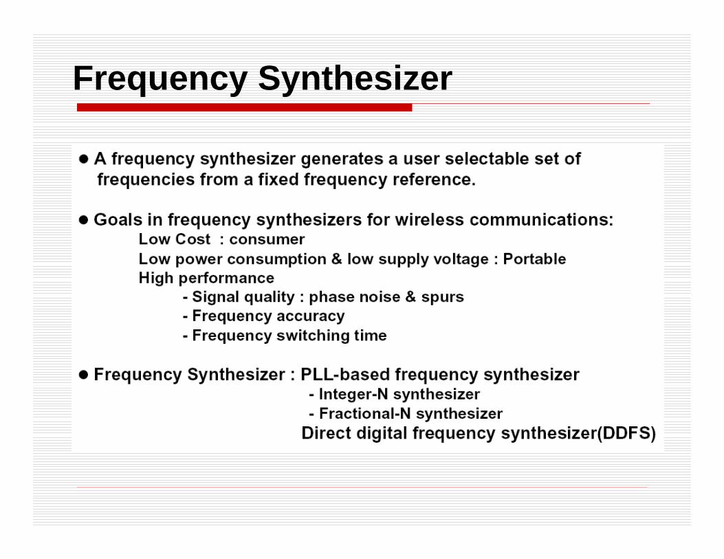
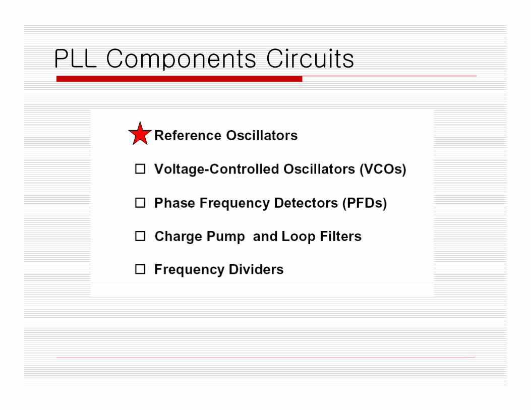
Frequency Synthesizer
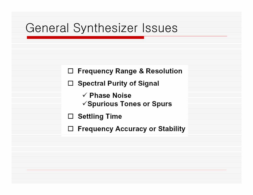
General Synthesizer Issues
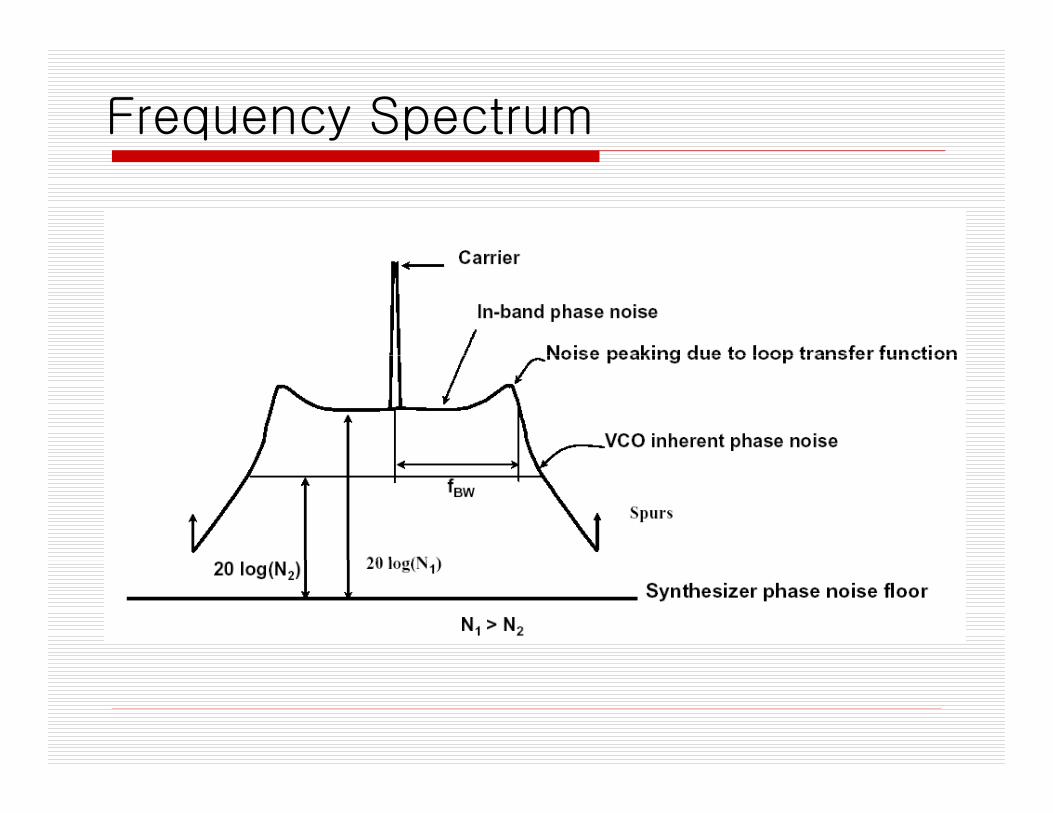
Frequency Spectrum
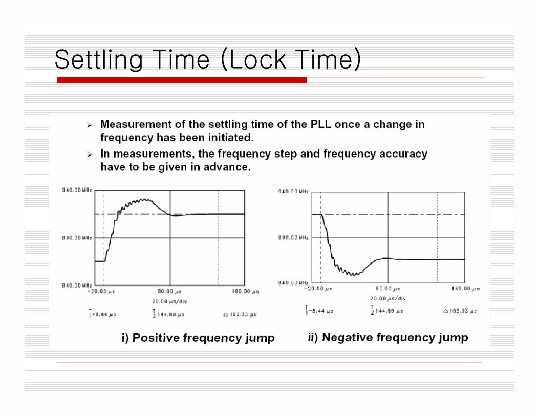
Settling Time (Lock Time)
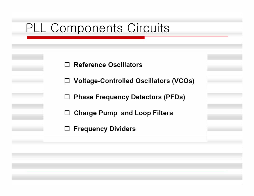
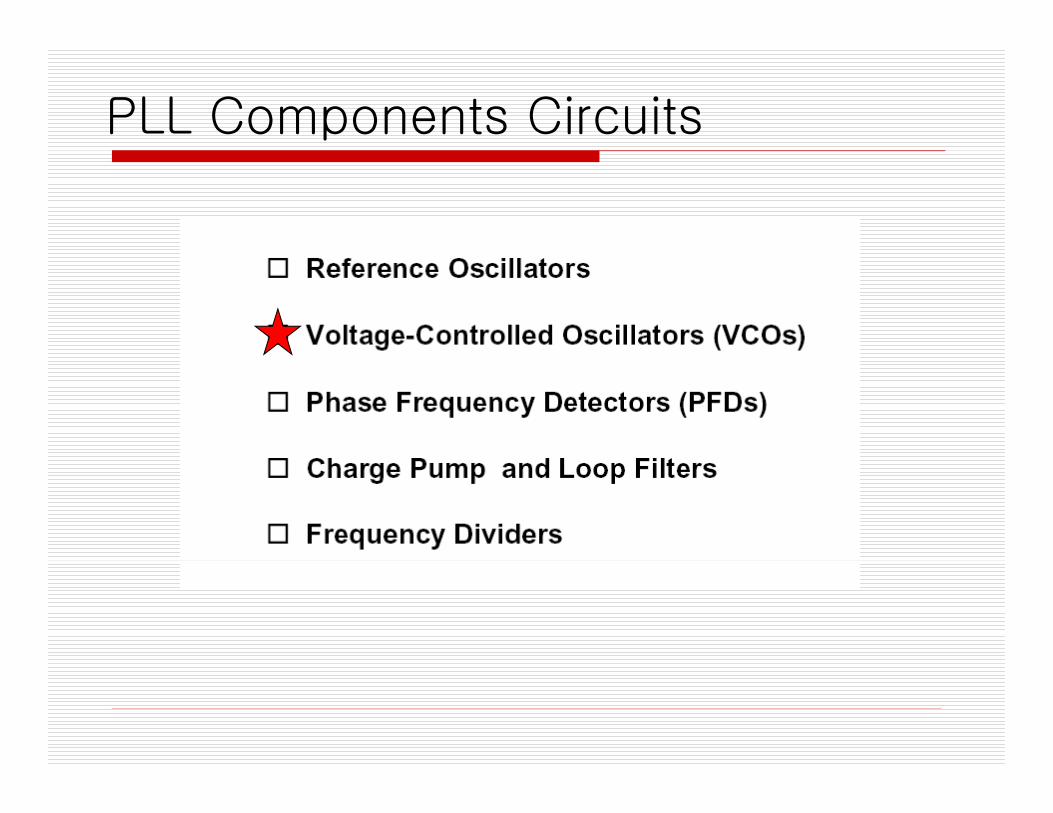
PLL Components Circuits
PLL Components Circuits
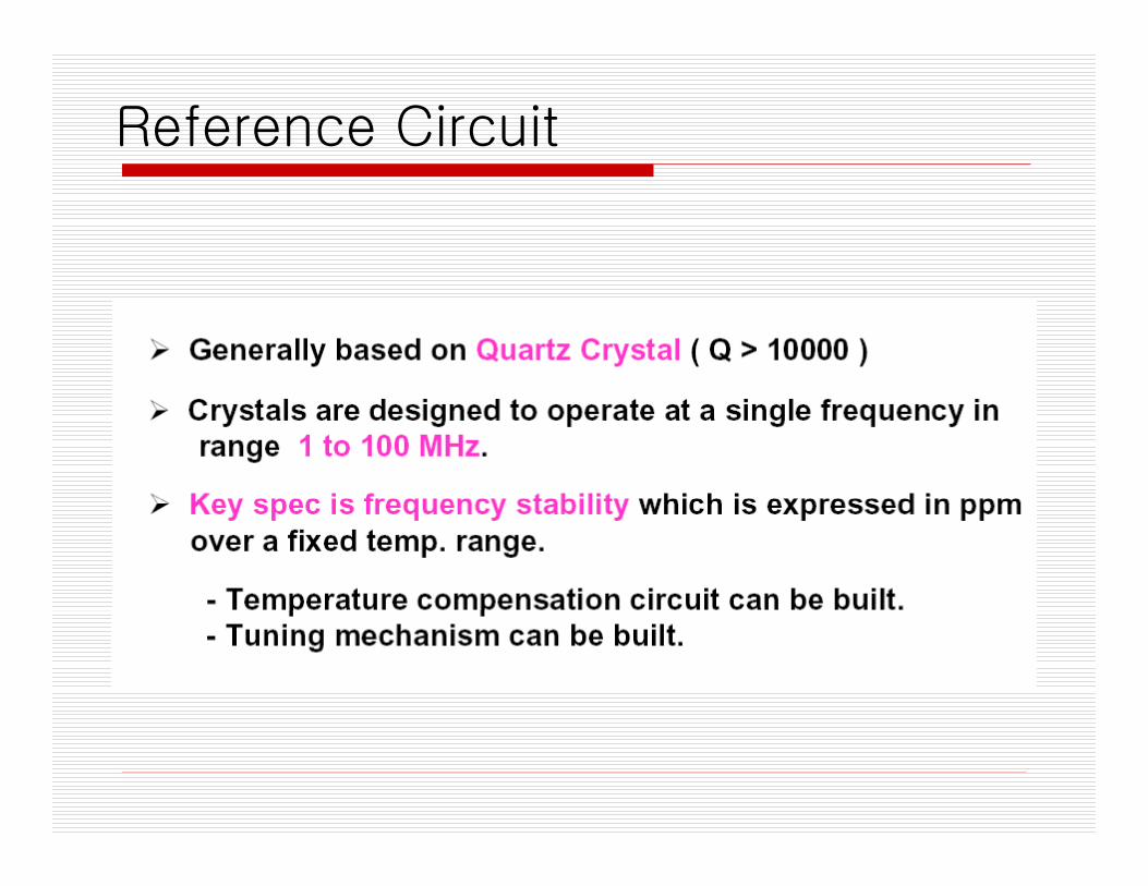
Reference Circuit
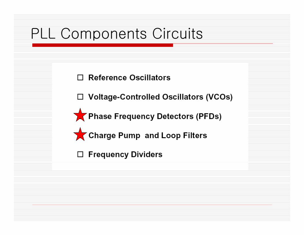
PLL Components Circuits
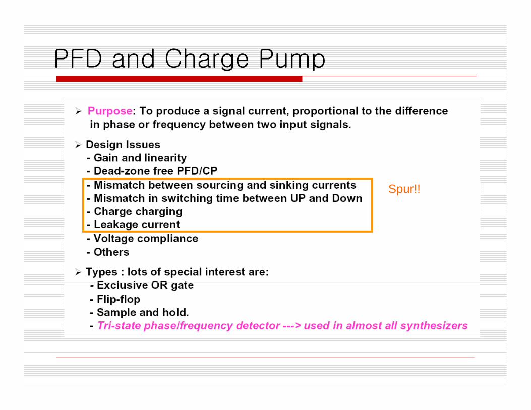
PFD and Charge Pump
Spur!!
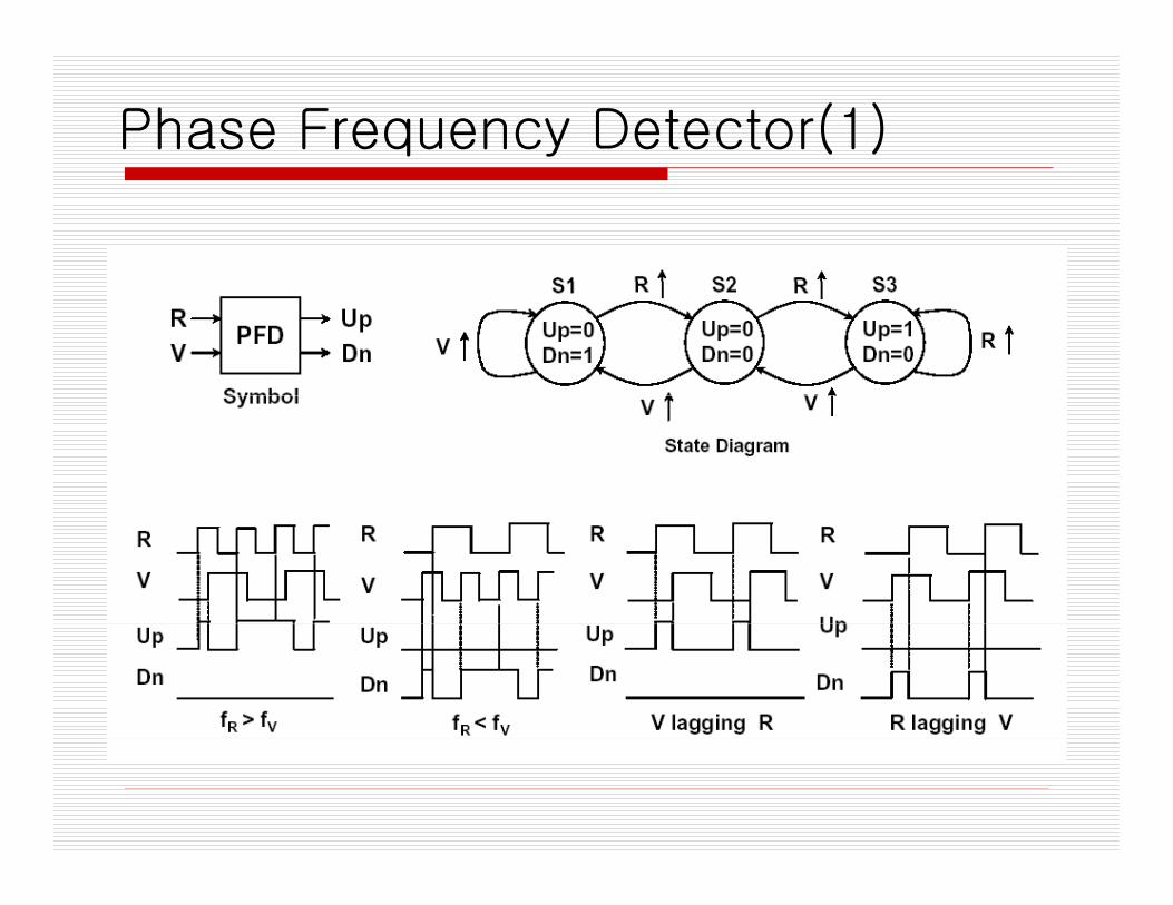
Phase Frequency Detector(1)
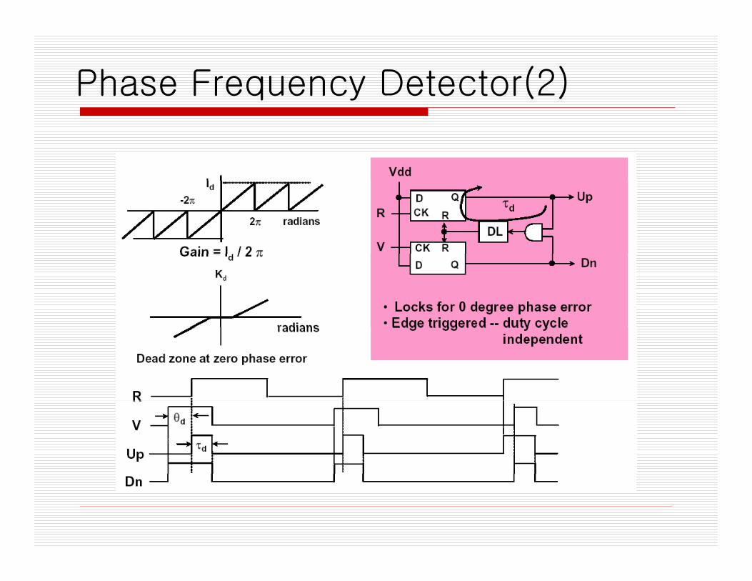
Phase Frequency Detector(2)
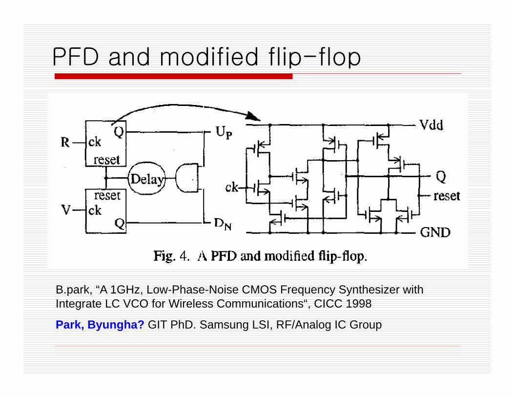
PFD and modified flip-flop
B.park, “A 1GHz, Low-Phase-Noise CMOS Frequency Synthesizer with Integrate LC VCO for Wireless Communications“, CICC 1998
Park Byungha? GIT PhD Samsung LSI RF/Analog IC GroupPark, Byungha? GIT PhD. Samsung LSI, RF/Analog IC Group
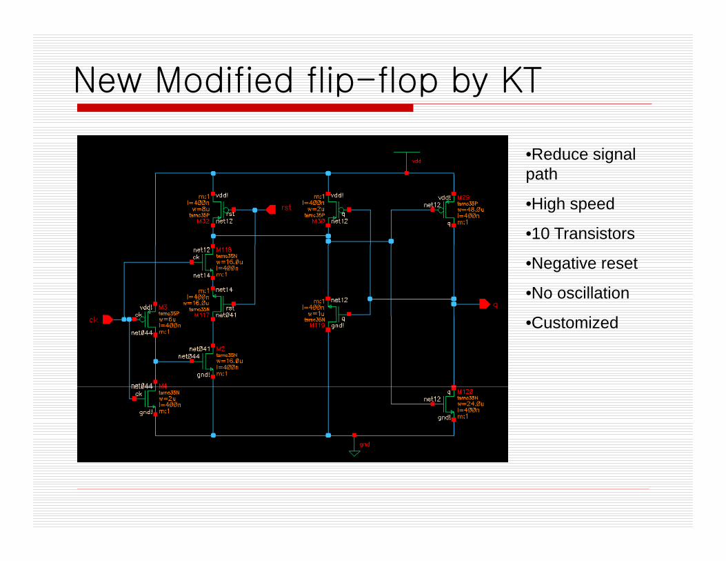
New Modified flip-flop by KT
•Reduce signal pathpath
•High speed
•10 Transistors
•Negative reset
•No oscillation
•Customized
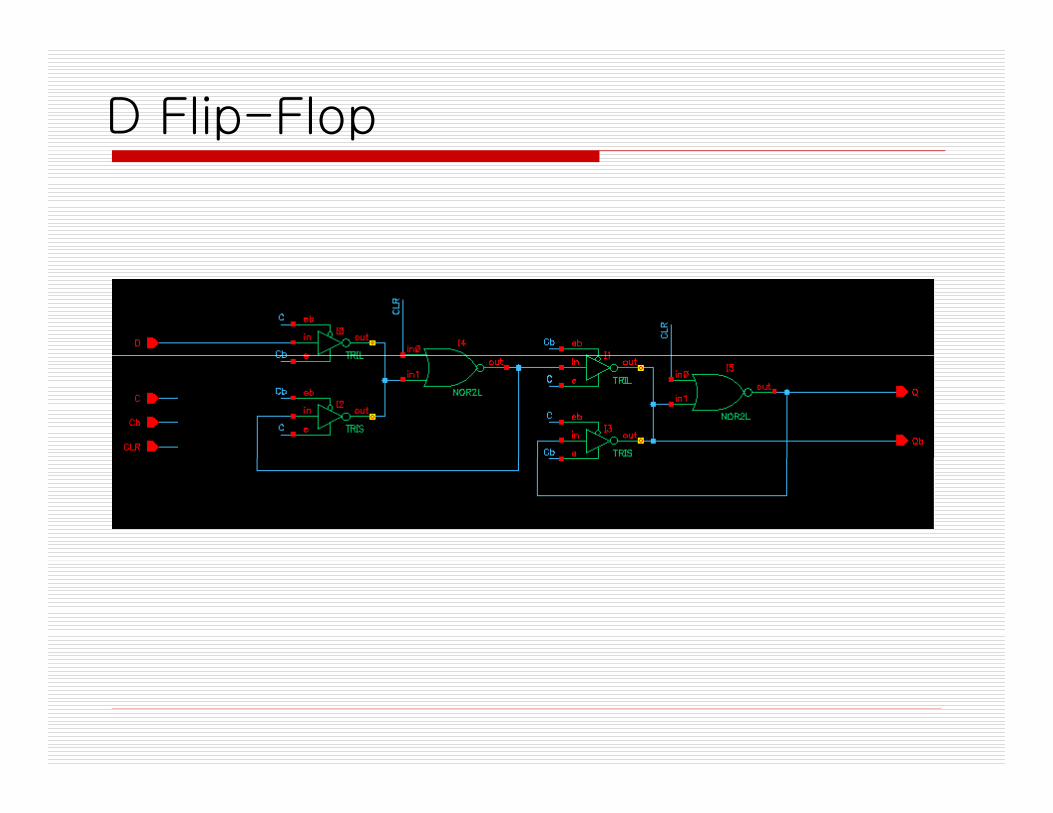
D Flip-Flop
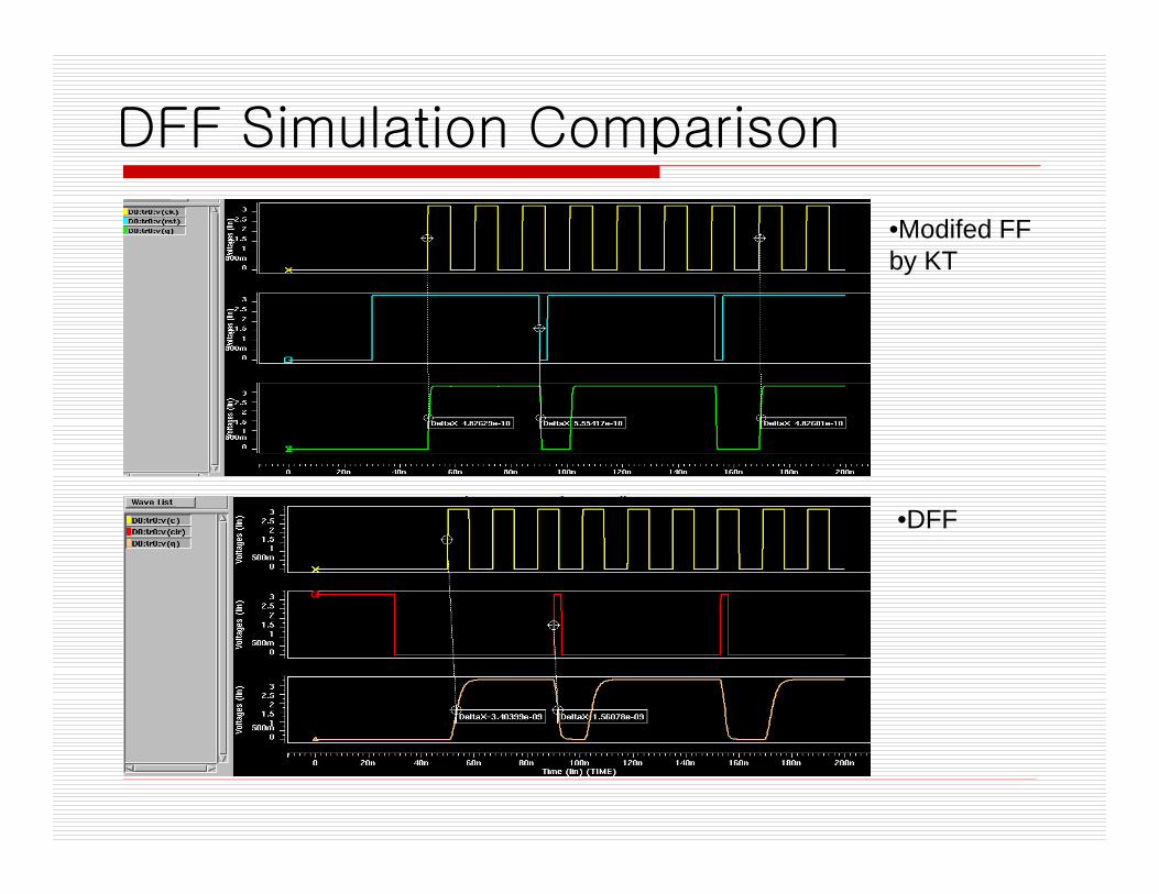
DFF Simulation Comparison
•Modifed FF by KT
•DFF
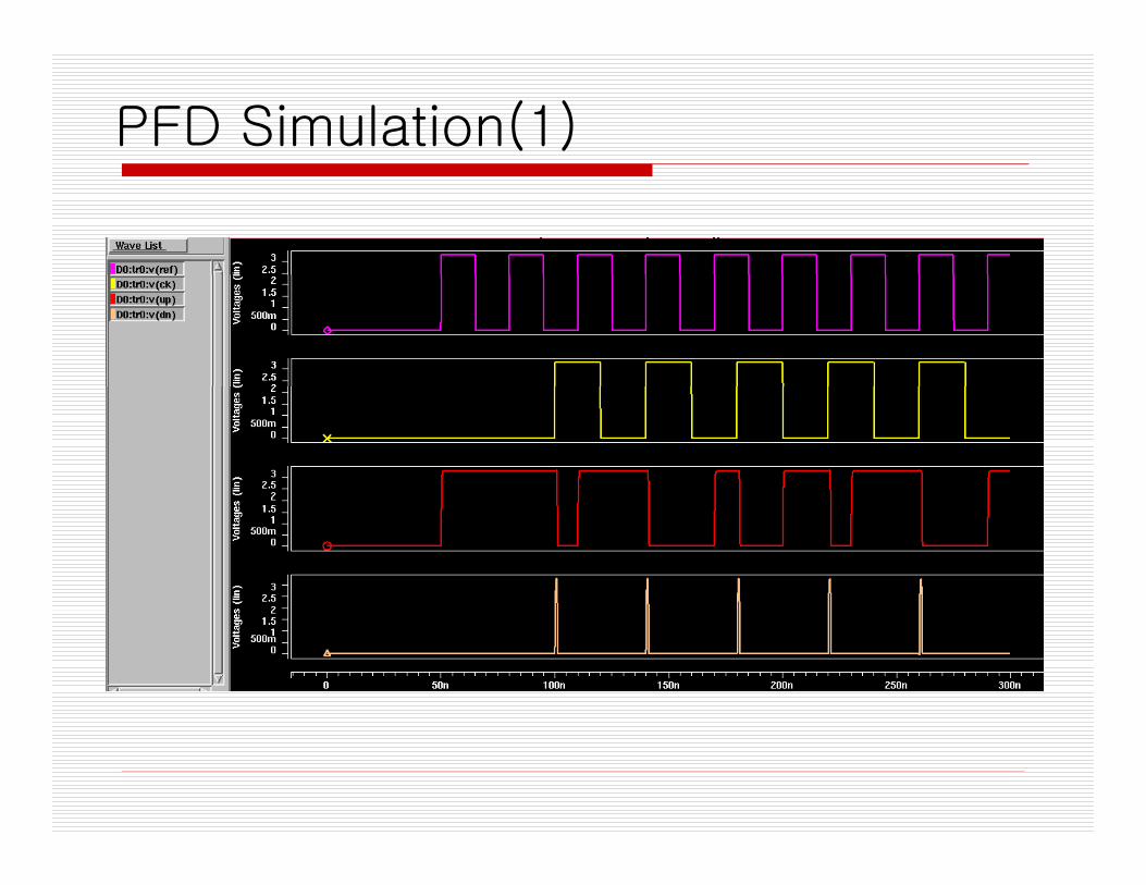
PFD Simulation(1)
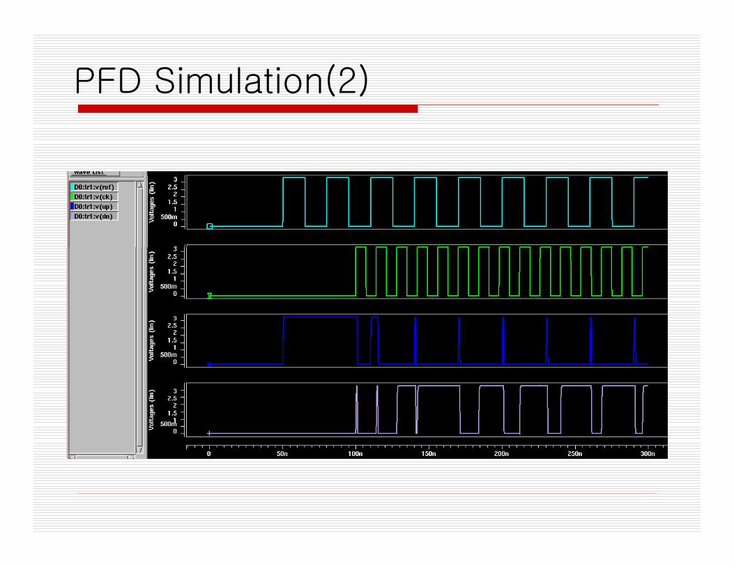
PFD Simulation(2)
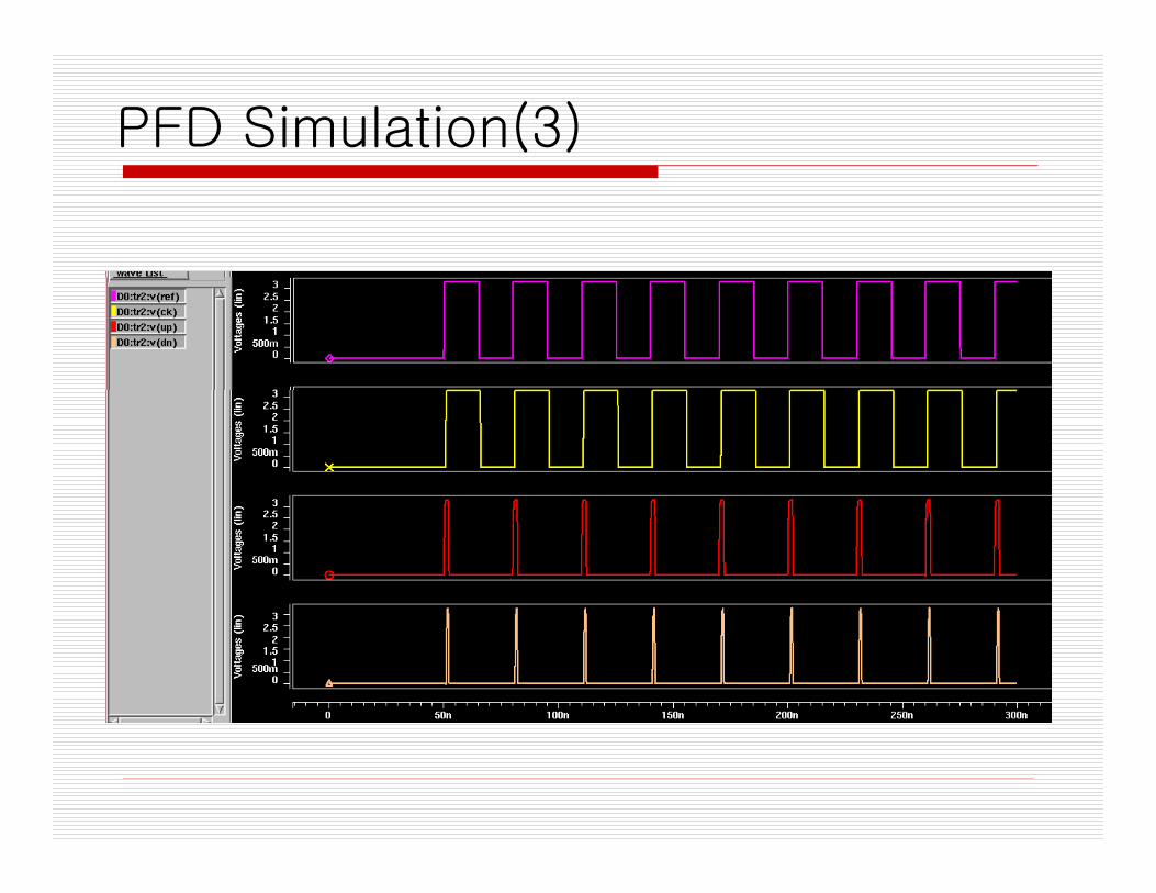
PFD Simulation(3)
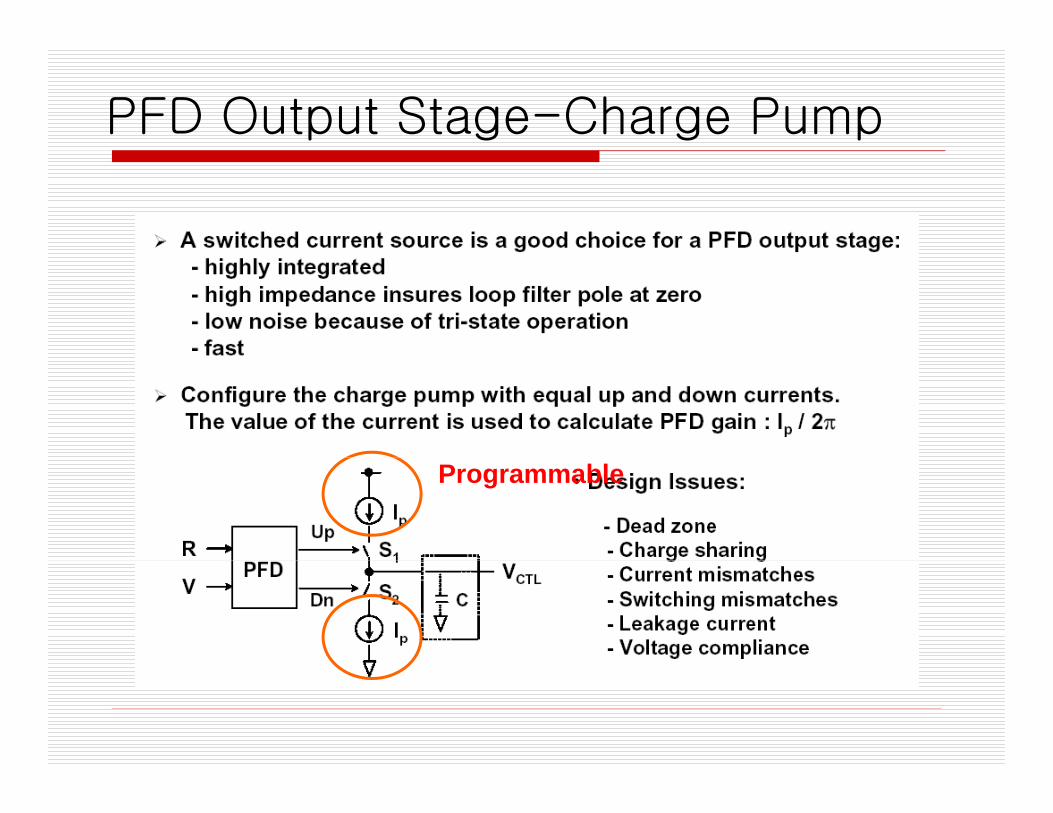
PFD Output Stage-Charge Pump
Programmable
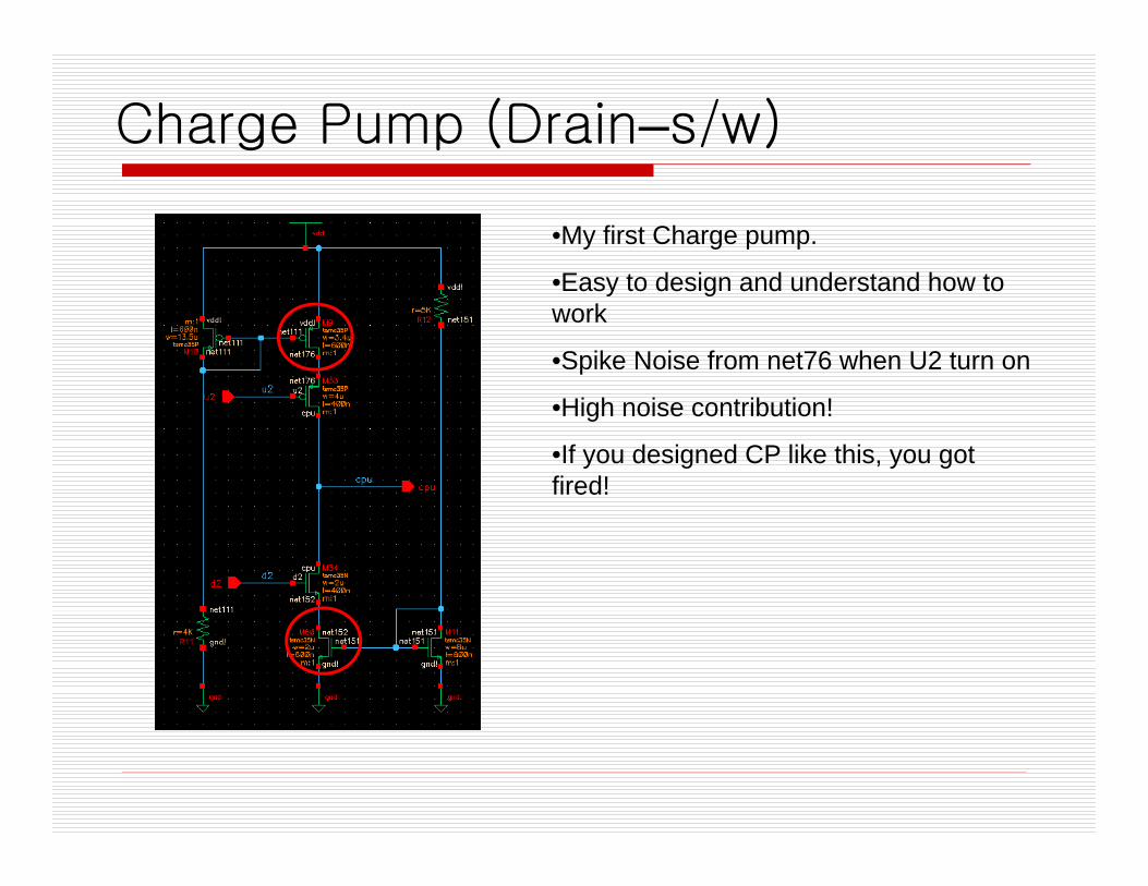
Charge Pump (Drain–s/w)
•My first Charge pump.
E t d i d d t d h t•Easy to design and understand how to work
•Spike Noise from net76 when U2 turn on
•High noise contribution!
•If you designed CP like this, you got fired!
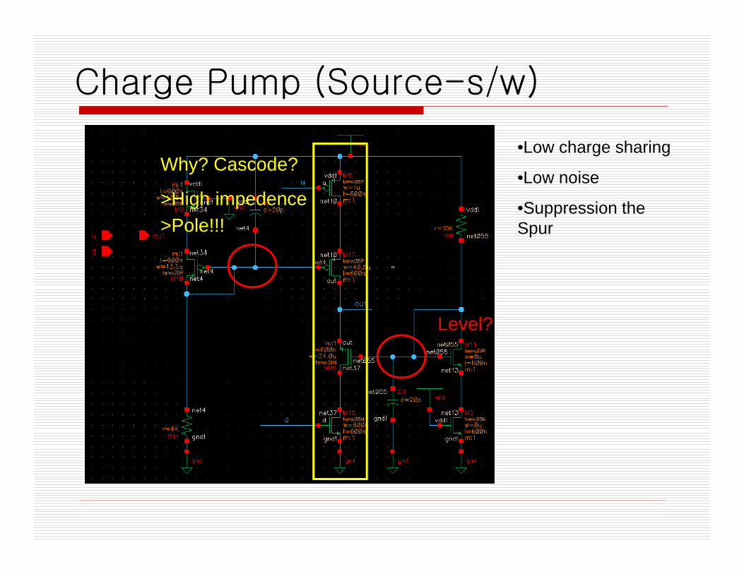
Charge Pump (Source-s/w)
•Low charge sharing
•Low noiseWhy? Cascode?
•Low noise
•Suppression the Spur
>High impedence>Pole!!!
Level?Level?
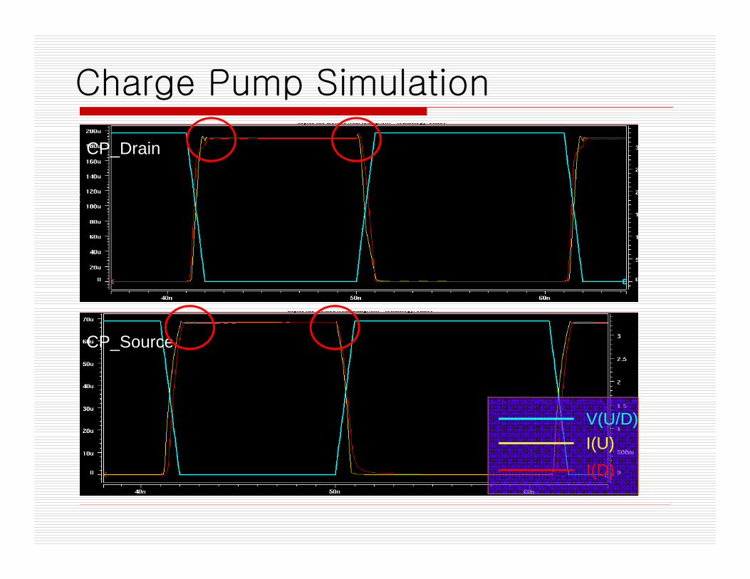
Charge Pump Simulation
CP_Drain
CP_Source
V(U/D)I(U)I(D)I(D)
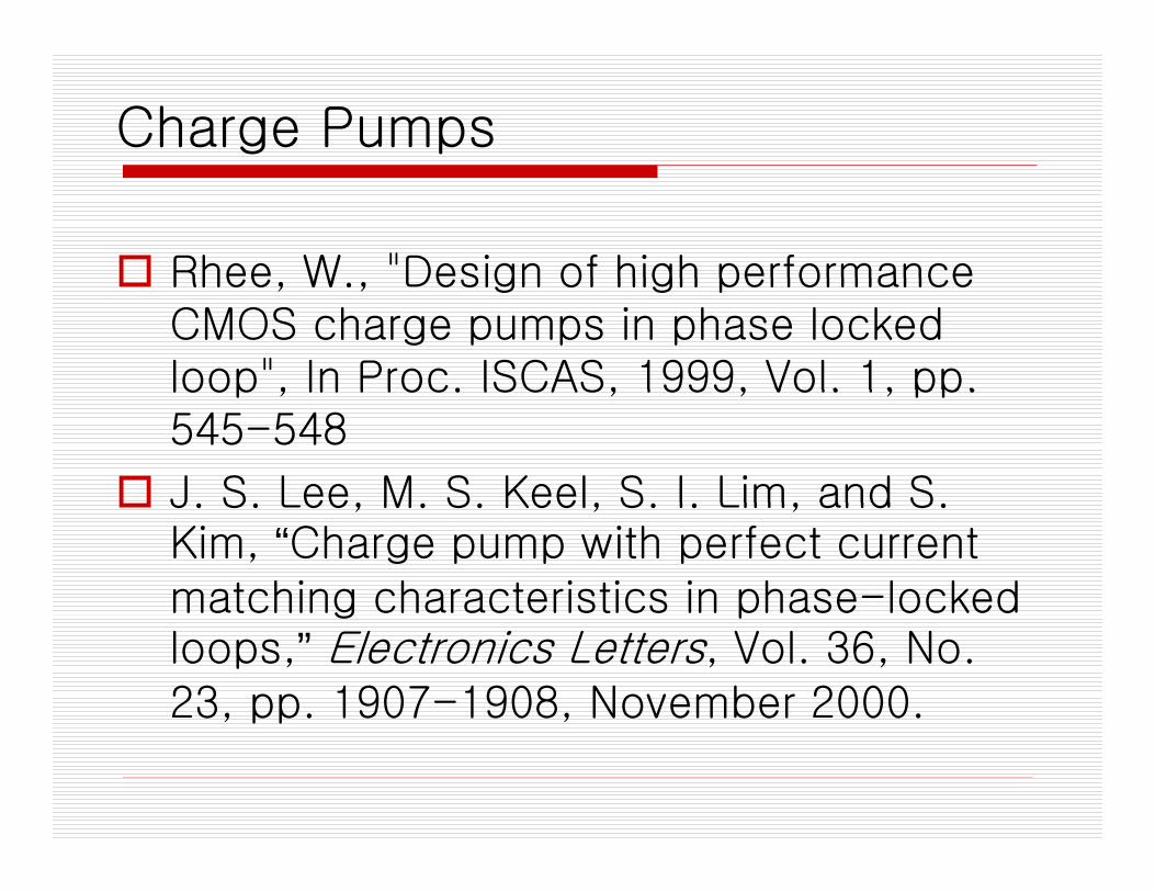
Charge Pumps
Rhee W "Design of high performanceRhee, W., Design of high performance CMOS charge pumps in phase locked loop", In Proc. ISCAS, 1999, Vol. 1, pp.loop , In Proc. ISCAS, 1999, Vol. 1, pp. 545-548
J S Lee M S Keel S I Lim and SJ. S. Lee, M. S. Keel, S. I. Lim, and S. Kim, “Charge pump with perfect current matching characteristics in phase-locked g ploops,” Electronics Letters, Vol. 36, No. 23, pp. 1907-1908, November 2000.
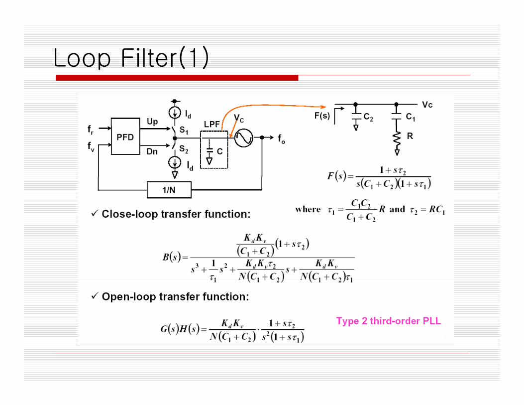
Loop Filter(1)
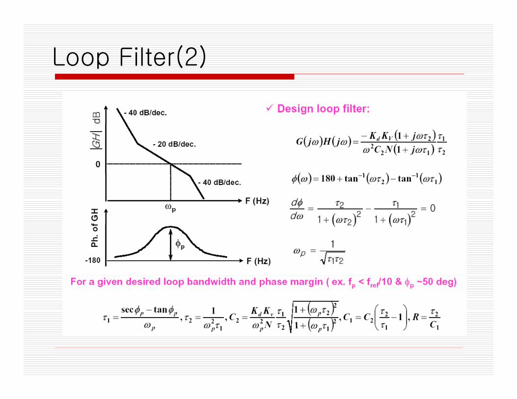
Loop Filter(2)
PLL Components Circuits
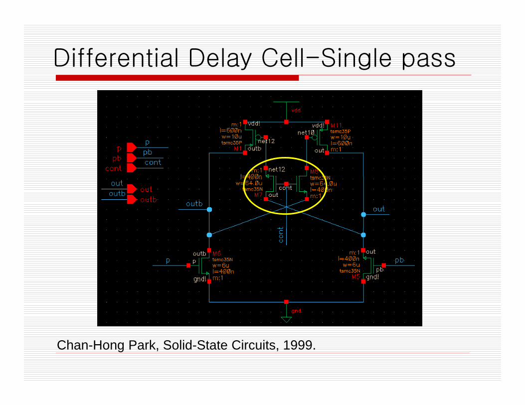
Differential Delay Cell-Single pass
Chan-Hong Park, Solid-State Circuits, 1999.
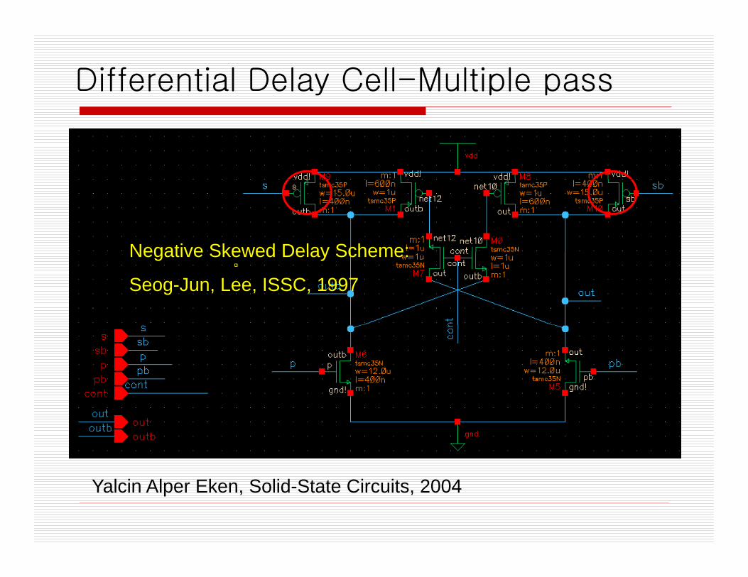
Differential Delay Cell-Multiple pass
Negative Skewed Delay Scheme:Negative Skewed Delay Scheme:
Seog-Jun, Lee, ISSC, 1997
Yalcin Alper Eken, Solid-State Circuits, 2004
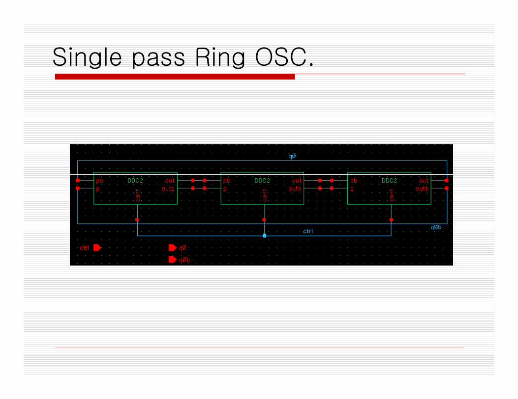
Single pass Ring OSC.
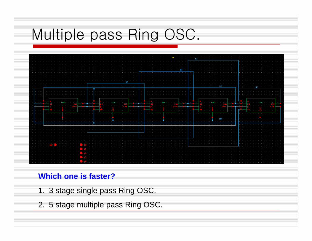
Multiple pass Ring OSC.
Which one is faster?
1. 3 stage single pass Ring OSC.
2. 5 stage multiple pass Ring OSC.
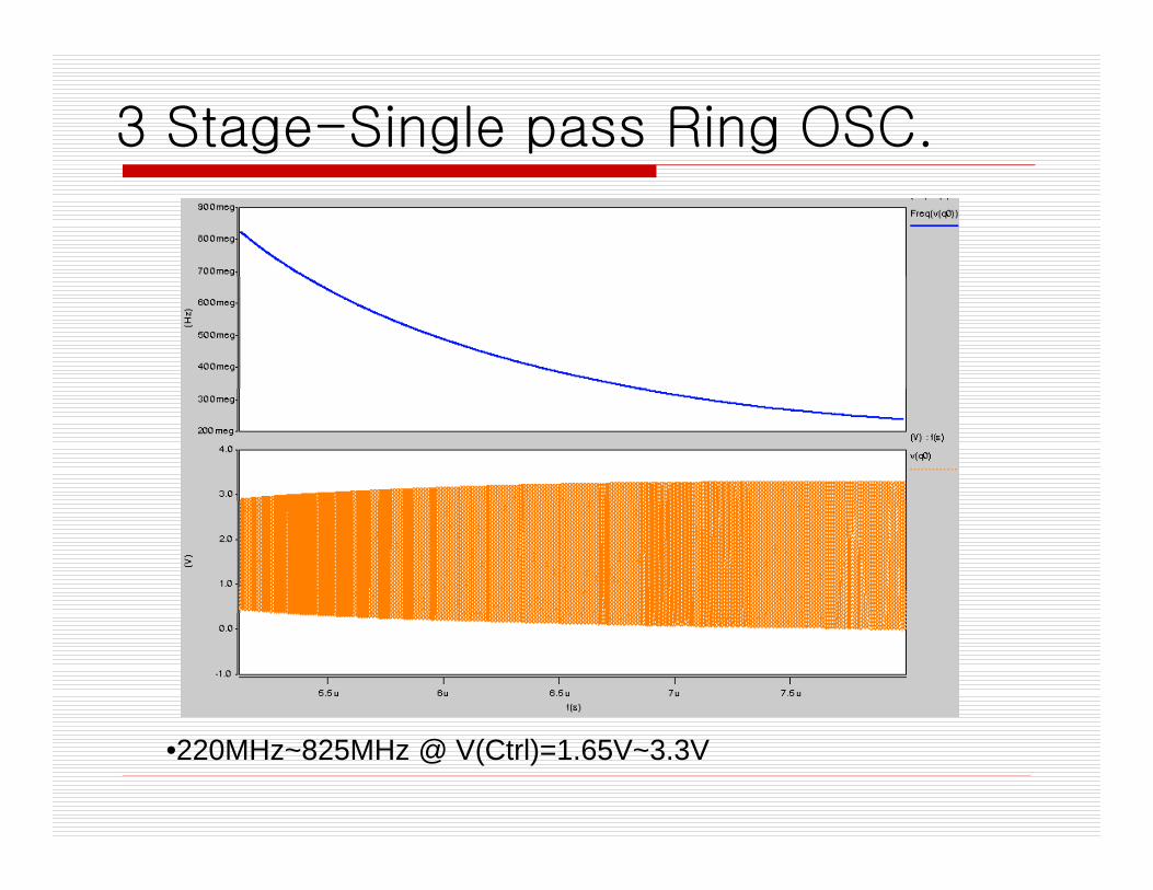
3 Stage-Single pass Ring OSC.
•220MHz~825MHz @ V(Ctrl)=1.65V~3.3V
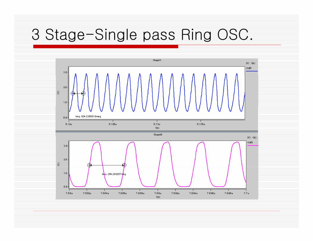
3 Stage-Single pass Ring OSC.
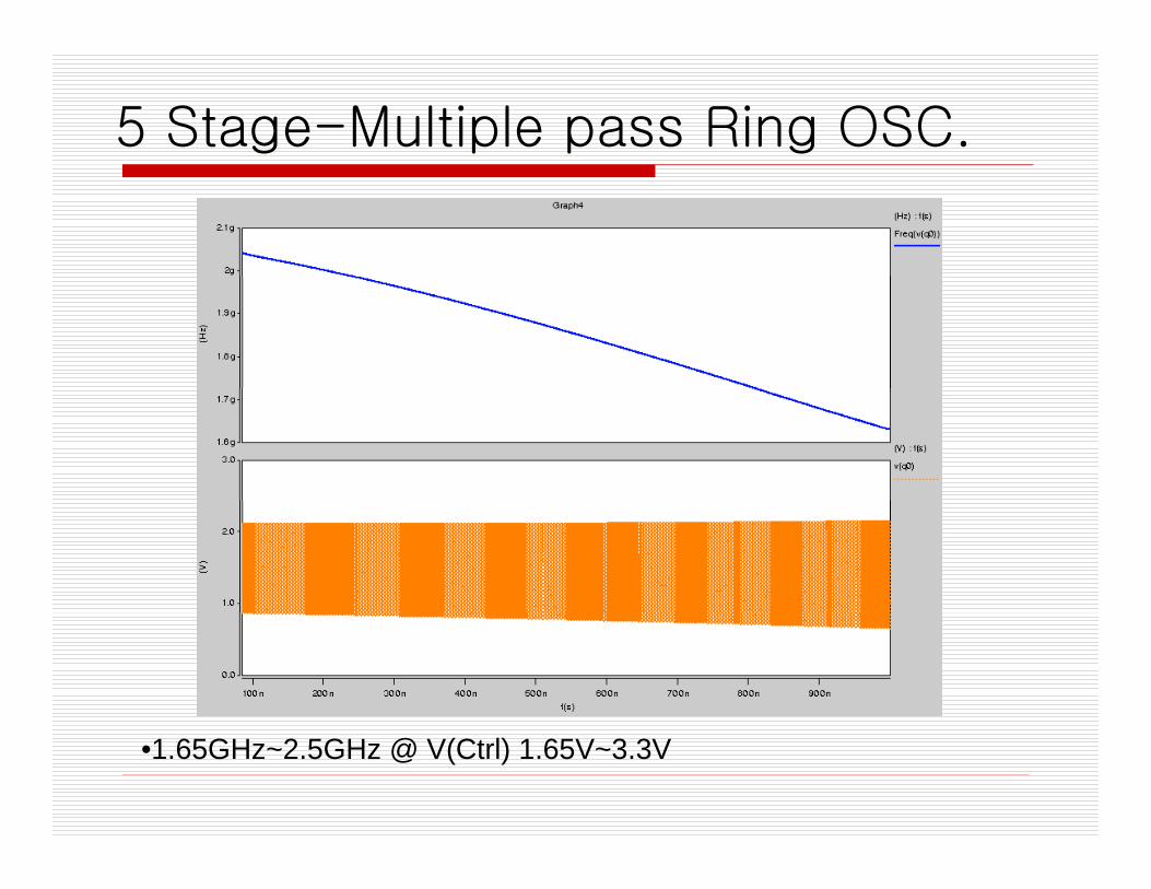
5 Stage-Multiple pass Ring OSC.
•1.65GHz~2.5GHz @ V(Ctrl) 1.65V~3.3V
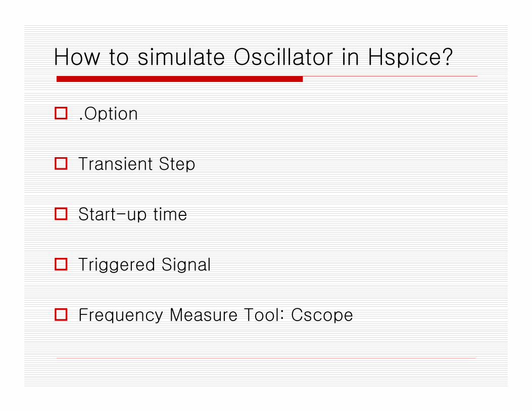
How to simulate Oscillator in Hspice?
.Option
Transient Step
Start-up time
Triggered Signal
Frequency Measure Tool: Cscope
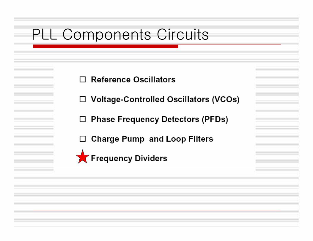
PLL Components Circuits
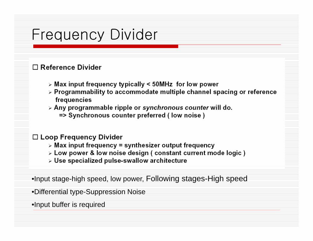
Frequency Divider
•Input stage-high speed, low power, Following stages-High speed•Differential type-Suppression Noise
•Input buffer is required
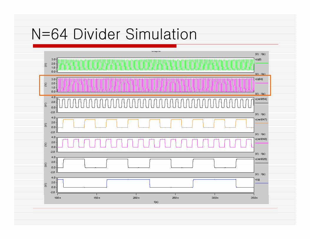
N=64 Divider Simulation
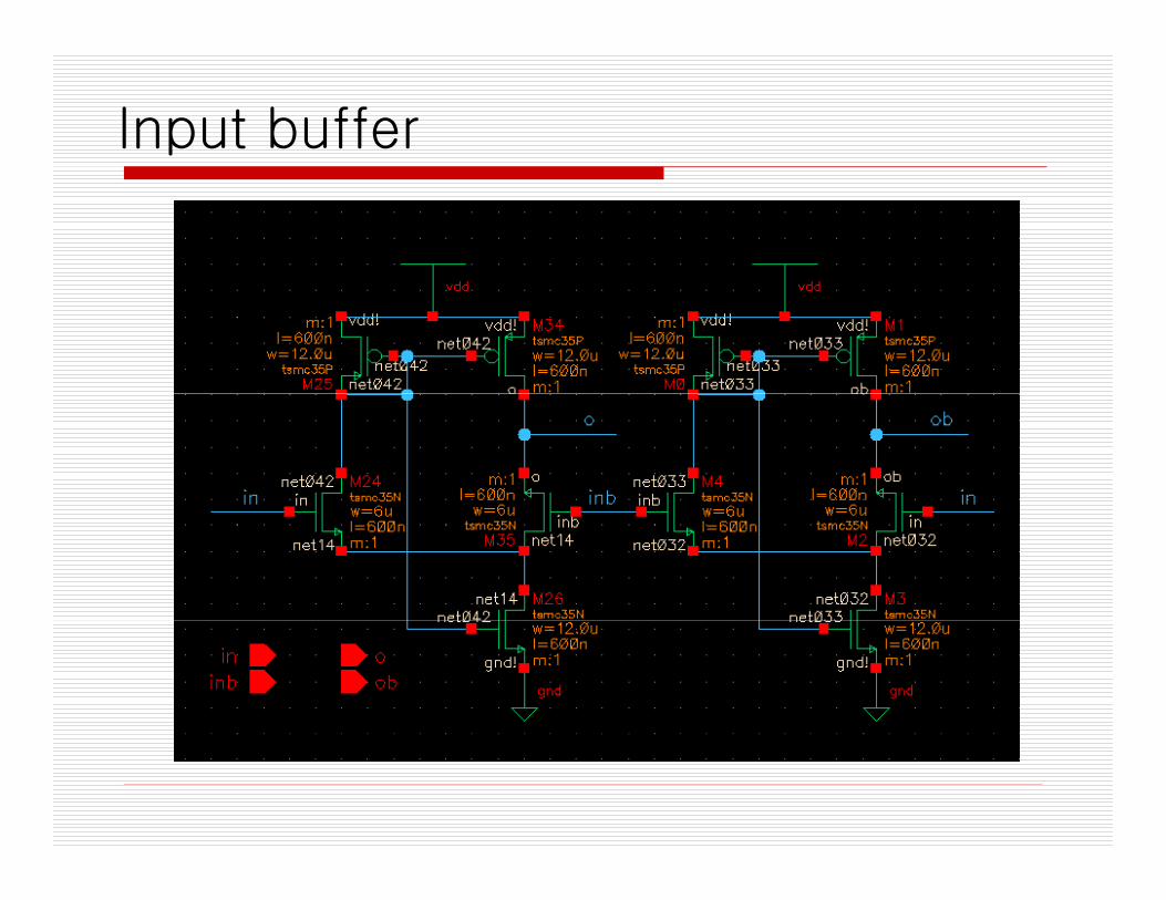
Input buffer
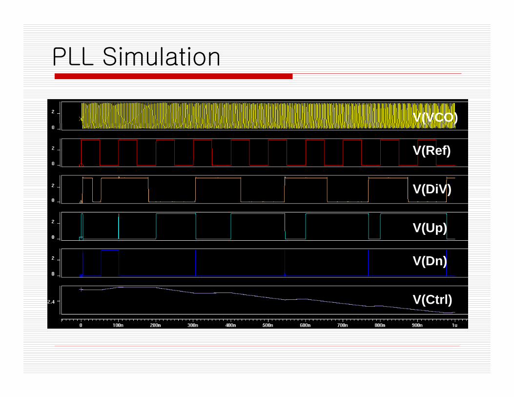
PLL Simulation
V(VCO)( )
V(Ref)
V(DiV)
V(U )V(Up)
V(Dn)
V(Ctrl)


![DESIGN AND ANALYSIS OF EFFICIENT PHASE LOCKED LOOP … · Phase Locked Loop (PLL) mainly for synchronization, clock synthesis, skew and jitter reduction [5]. Phase locked loops find](https://img.pdfslide.us/doc/110x75/5e9d540ca2a49a4e746bfacd/design-and-analysis-of-efficient-phase-locked-loop-phase-locked-loop-pll-mainly.jpg)

![PHASE-LOCKED LOOP SIMULATIONS USING T-SPICE Contents · Phase Lock Loop Simulations [1] PHASE-LOCKED LOOP SIMULATIONS USING T-SPICE Contents: • A Brief Introduction to T-Spice •](https://img.pdfslide.us/doc/110x75/5adfd3d67f8b9a1c248c7fb4/phase-locked-loop-simulations-using-t-spice-lock-loop-simulations-1-phase-locked.jpg)