Embed Size (px)
Citation preview
PHASE LOCKED LOOP DESIGN
by
Kristen Elserougi, Ranil Fernando, Luca Wei
SENIOR DESIGN PROJECT REPORT
Submitted in partial fulfillment of the requirements for the degree of
Bachelor of Science in Electrical Engineering School of Engineering Santa Clara University
Santa Clara, California
June 20, 2006
1
Abstract
Our team chose to do a complete mixed signal IC design process. With this purpose, we
decided to design a Phase Locked Loop (PLL) because the design process would incorporate
topics from digital, analog, IC design, and control systems theory. This range of topics is an
adequate way to incorporate the primary electrical engineering theories into one project.
A PLL is a closed loop frequency system that locks the phase of an output signal to an
input reference signal. The term “lock” refers to a constant or zero phase difference between two
signals. The signal from the feedback path, ffb, is compared to the input reference signal, fref,
until the two signals are locked. If the phase is unmatched, this is called the unlocked state, and
the signal is sent to each component in the loop to correct the phase difference. These
components consist of the Phase Frequency Detector (PFD), the charge pump (CP), the low pass
filter (LPF), and the voltage controlled oscillator (VCO). The PFD detects any phase differences
in fref and ffb and then generates an error signal. According to that error signal the CP either
increases or decreases the amount of charge to the LPF. This amount of charge either speeds up
or slows down the VCO. The loop continues in this process until the phase difference between
fref and ffb is zero or constant—this is the locked mode. After the loop has attained a locked
status, the loop still continues in the process but the output of each component is constant. The
output signal, fout, has the same phase and/or frequency as fref.
This design flow process included design and simulation of the components/system and it
also included the VCO layout. The application we chose in designing the PLL was a clock
generator and frequency synthesizer. A clock generator generates a digital clock signal and a
frequency synthesizer generates a frequency that can have a different frequency from the original
reference signal.

2
Acknowledgments
We would like to thank Dr. Shoba Krishnan for her advising. She helped our team with
the theory, design, and presentation of our project. She was a major contributing factor to the
success of this project and to our team. Thank you, Dr. Shoba Krishnan.
3
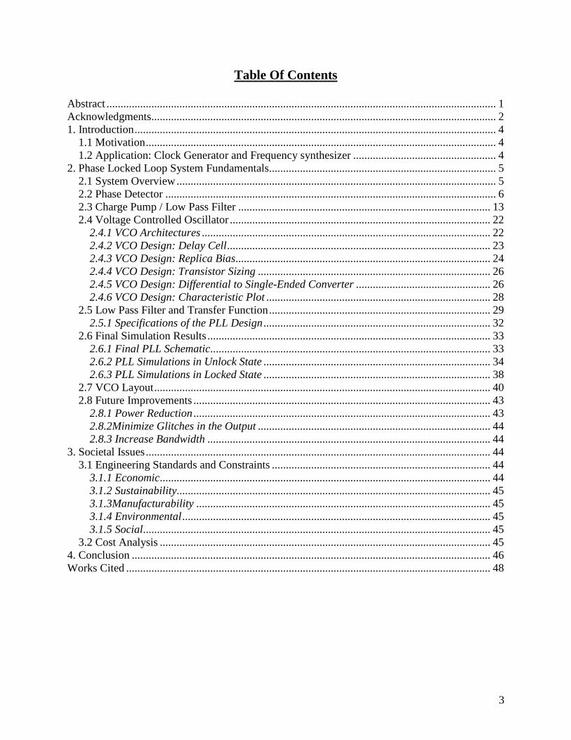
Table Of Contents
Abstract ........................................................................................................................................... 1 Acknowledgments........................................................................................................................... 2 1. Introduction................................................................................................................................. 4
1.1 Motivation............................................................................................................................. 4 1.2 Application: Clock Generator and Frequency synthesizer ................................................... 4
2. Phase Locked Loop System Fundamentals................................................................................. 5 2.1 System Overview.................................................................................................................. 5 2.2 Phase Detector ...................................................................................................................... 6 2.3 Charge Pump / Low Pass Filter .......................................................................................... 13 2.4 Voltage Controlled Oscillator ............................................................................................. 22
2.4.1 VCO Architectures ....................................................................................................... 22 2.4.2 VCO Design: Delay Cell.............................................................................................. 23 2.4.3 VCO Design: Replica Bias........................................................................................... 24 2.4.4 VCO Design: Transistor Sizing ................................................................................... 26 2.4.5 VCO Design: Differential to Single-Ended Converter ................................................ 26 2.4.6 VCO Design: Characteristic Plot ................................................................................ 28
2.5 Low Pass Filter and Transfer Function............................................................................... 29 2.5.1 Specifications of the PLL Design................................................................................. 32
2.6 Final Simulation Results..................................................................................................... 33 2.6.1 Final PLL Schematic.................................................................................................... 33 2.6.2 PLL Simulations in Unlock State ................................................................................. 34 2.6.3 PLL Simulations in Locked State ................................................................................. 38
2.7 VCO Layout........................................................................................................................ 40 2.8 Future Improvements .......................................................................................................... 43
2.8.1 Power Reduction .......................................................................................................... 43 2.8.2Minimize Glitches in the Output ................................................................................... 44 2.8.3 Increase Bandwidth ..................................................................................................... 44
3. Societal Issues........................................................................................................................... 44 3.1 Engineering Standards and Constraints .............................................................................. 44
3.1.1 Economic...................................................................................................................... 44 3.1.2 Sustainability................................................................................................................ 45 3.1.3Manufacturability ......................................................................................................... 45 3.1.4 Environmental.............................................................................................................. 45 3.1.5 Social............................................................................................................................ 45
3.2 Cost Analysis ...................................................................................................................... 45 4. Conclusion ................................................................................................................................ 46 Works Cited .................................................................................................................................. 48
4
1. Introduction
A Phase Locked Loop (PLL) is a system that locks the phase or frequency to an input
reference signal. PLL’s are widely used in computer, radio, and telecommunications systems
where it is necessary to stabilize a generated signal or to detect signals.
1.1 Motivation
Our team chose to complete a mixed signal IC design process. With this purpose, we
decided to design a Phase Locked Loop (PLL) because the design process would incorporate
topics from digital, analog, IC design, and control systems theory. This range of topics is an
adequate way to incorporate the primary electrical engineering theories into one project.
Furthermore, designing a system that incorporates many different topics from our schooling
allows us to apply our knowledge to a real world technology.
1.2 Application: Clock Generator and Frequency synthesizer
The input of the PLL is a reference frequency, fref from the user. The VCO sends another
input frequency, ffb into the PFD to compare the reference frequency with the VCO frequency.
After the PLL corrects the frequency to have zero offset phase, or to be in the lock mode, the
frequency is taken as an output at the VCO, fout. Therefore, a frequency is synthesized. (Note:
Constraints on the input frequency, fref, must be within the tuning range of the VCO and the PLL
as a whole system. The tuning range is the range in which the VCO functions properly. If fref
isn’t within this tuning range, a divider is necessary). A divider can be used in the feedback path
to synthesize a frequency different than that of the reference signal. Furthermore, since the
reference signal is a clock signal, the output is also a clock signal—thus a clock generator.
5
2. Phase Locked Loop System Fundamentals
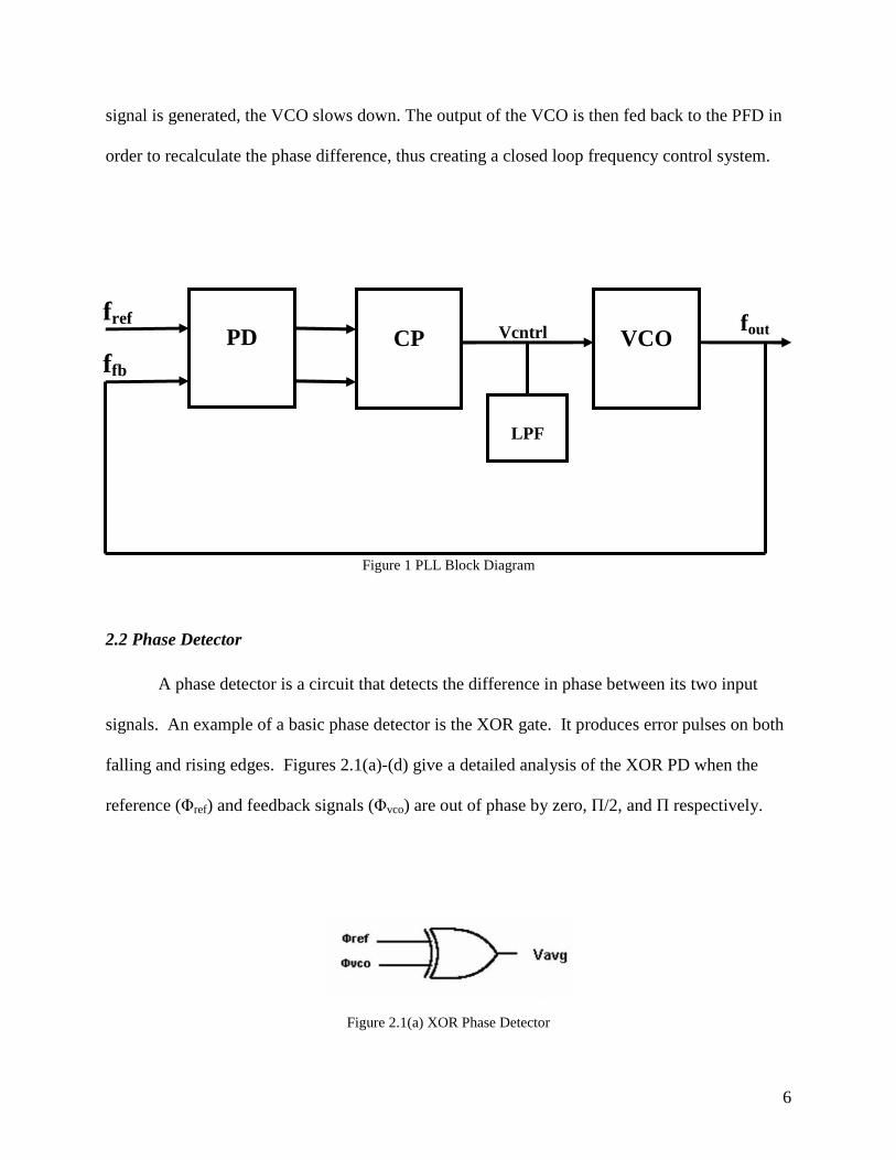
2.1 System Overview
A PLL is a negative feedback control system circuit. As the name implies, the purpose of
a PLL is to generate a signal in which the phase is the same as the phase of a reference signal.
This is done after many iterations of comparing the reference and feedback signals (refer to
Figure 1). The overall goal of the PLL is to match the reference and feedback signals in phase—
this is the lock mode. After this, the PLL continues to compare the two signals but since they are
in lock mode, the PLL output is constant. A basic form of a PLL consists of four main blocks:
1. Phase Detector or Phase Frequency Detector (PD or PFD) 2. Charge Pump (CP) 3. Low Pass Filter (LPF) 4. Voltage Controlled Oscillator (VCO)
The phase frequency detector, PFD, measures the difference in phase between the
reference and feedback signals. If there is a phase difference between the two signals, it
generates “up” or “down” synchronized signals to the charge pump/ low pass filter. If the error
signal from the PFD is an “up” signal, then the charge pump pumps charge onto the LPF
capacitor which increases the control voltage, Vcntrl. On the contrary, if the error signal from
the PFD is a “down” signal, the charge pump removes charge from the LPF capacitor, which
decreases Vcntrl. Vcntrl is the input to the VCO. Thus, the LPF is necessary to only allow DC
signals into the VCO and is also necessary to store the charge from the CP. The purpose of the
VCO is to either speed up or slow down the feedback signal according to the error generated by
the PFD. If the PFD generates an “up” signal, the VCO speeds up. On the contrary, if a “down”
6
ffb
fout Vcntrl
PD
CP
VCO
LPF
fref
signal is generated, the VCO slows down. The output of the VCO is then fed back to the PFD in
order to recalculate the phase difference, thus creating a closed loop frequency control system.
Figure 1 PLL Block Diagram
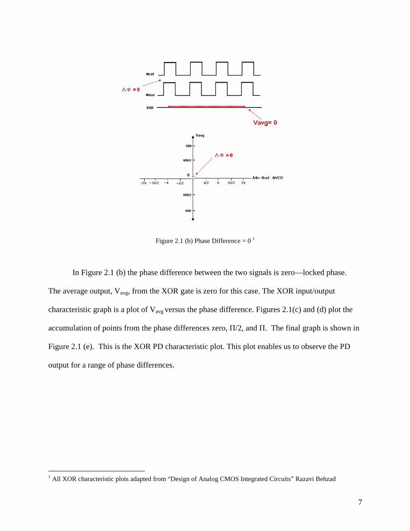
2.2 Phase Detector
A phase detector is a circuit that detects the difference in phase between its two input
signals. An example of a basic phase detector is the XOR gate. It produces error pulses on both
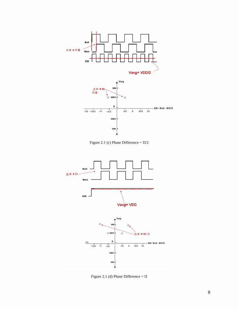
falling and rising edges. Figures 2.1(a)-(d) give a detailed analysis of the XOR PD when the
reference (Φref) and feedback signals (Φvco) are out of phase by zero, Π/2, and Π respectively.
Figure 2.1(a) XOR Phase Detector
7
Figure 2.1 (b) Phase Difference = 0 1
In Figure 2.1 (b) the phase difference between the two signals is zero—locked phase.
The average output, Vavg, from the XOR gate is zero for this case. The XOR input/output
characteristic graph is a plot of Vavg versus the phase difference. Figures 2.1(c) and (d) plot the
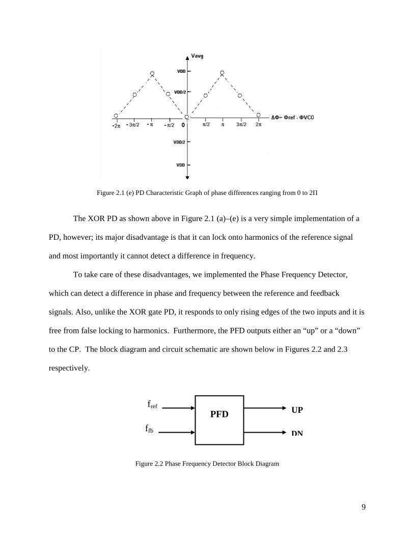
accumulation of points from the phase differences zero, Π/2, and Π. The final graph is shown in
Figure 2.1 (e). This is the XOR PD characteristic plot. This plot enables us to observe the PD
output for a range of phase differences.
1 All XOR characteristic plots adapted from “Design of Analog CMOS Integrated Circuits” Razavi Behzad
8
Figure 2.1 (c) Phase Difference = Π/2
Figure 2.1 (d) Phase Difference = Π
9
Figure 2.1 (e) PD Characteristic Graph of phase differences ranging from 0 to 2Π
The XOR PD as shown above in Figure 2.1 (a)–(e) is a very simple implementation of a
PD, however; its major disadvantage is that it can lock onto harmonics of the reference signal
and most importantly it cannot detect a difference in frequency.
To take care of these disadvantages, we implemented the Phase Frequency Detector,
which can detect a difference in phase and frequency between the reference and feedback
signals. Also, unlike the XOR gate PD, it responds to only rising edges of the two inputs and it is
free from false locking to harmonics. Furthermore, the PFD outputs either an “up” or a “down”
to the CP. The block diagram and circuit schematic are shown below in Figures 2.2 and 2.3
respectively.
Figure 2.2 Phase Frequency Detector Block Diagram
UP
PFD fref
f fb DN
10
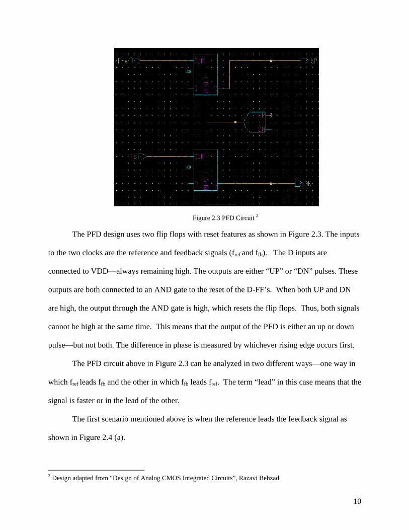
Figure 2.3 PFD Circuit 2
The PFD design uses two flip flops with reset features as shown in Figure 2.3. The inputs
to the two clocks are the reference and feedback signals (fref and ffb). The D inputs are
connected to VDD—always remaining high. The outputs are either “UP” or “DN” pulses. These
outputs are both connected to an AND gate to the reset of the D-FF’s. When both UP and DN
are high, the output through the AND gate is high, which resets the flip flops. Thus, both signals
cannot be high at the same time. This means that the output of the PFD is either an up or down
pulse—but not both. The difference in phase is measured by whichever rising edge occurs first.
The PFD circuit above in Figure 2.3 can be analyzed in two different ways—one way in
which fref leads ffb and the other in which ffb leads fref. The term “lead” in this case means that the
signal is faster or in the lead of the other.
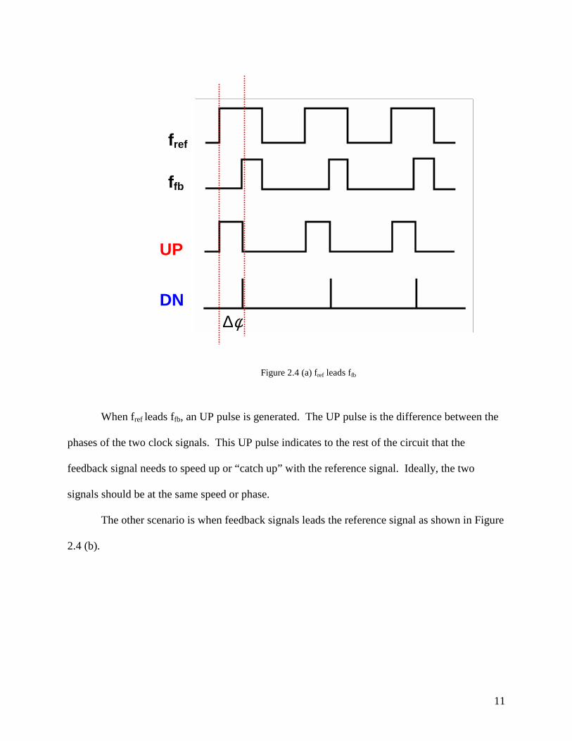
The first scenario mentioned above is when the reference leads the feedback signal as
shown in Figure 2.4 (a).
2 Design adapted from “Design of Analog CMOS Integrated Circuits”, Razavi Behzad
11
Figure 2.4 (a) fref leads ffb
When fref leads ffb, an UP pulse is generated. The UP pulse is the difference between the
phases of the two clock signals. This UP pulse indicates to the rest of the circuit that the
feedback signal needs to speed up or “catch up” with the reference signal. Ideally, the two
signals should be at the same speed or phase.
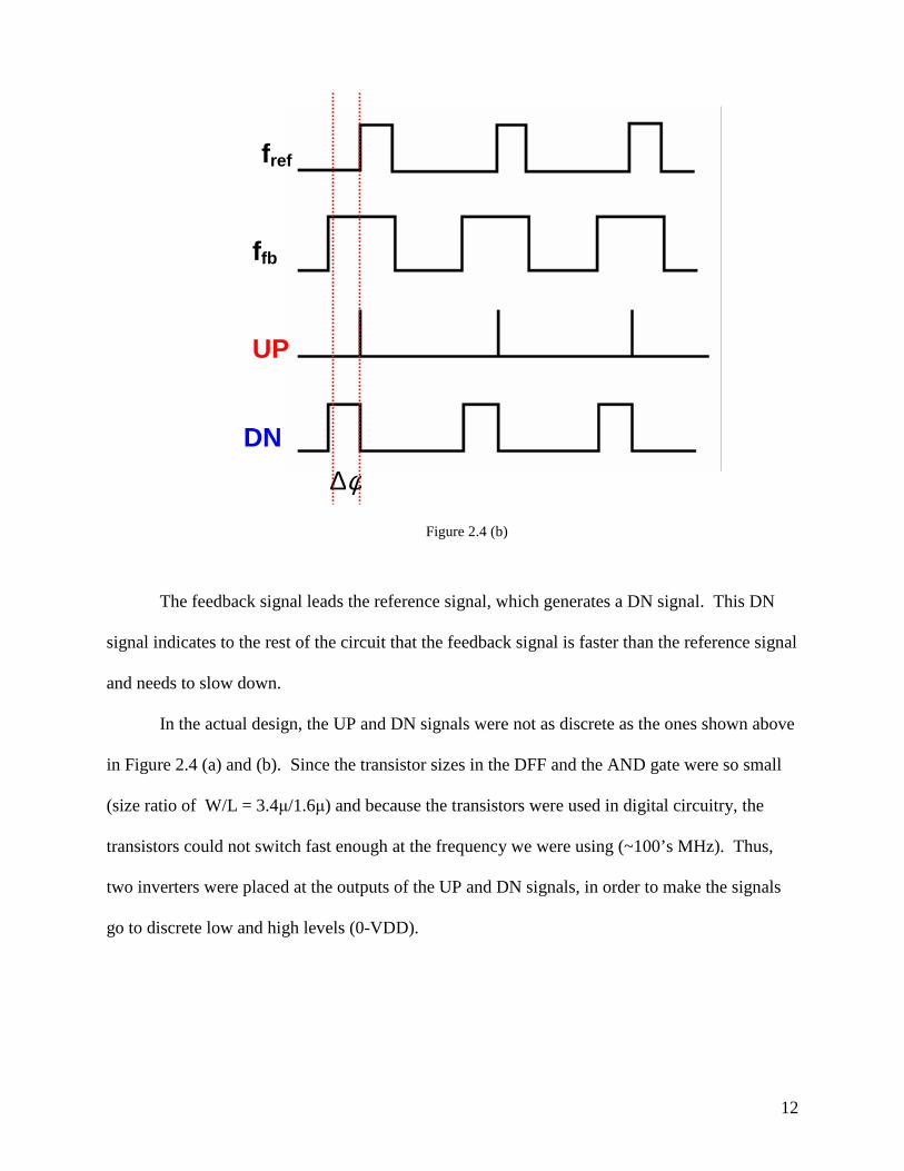
The other scenario is when feedback signals leads the reference signal as shown in Figure
2.4 (b).
fref
UP
ffb
DN φ∆
12
Figure 2.4 (b)
The feedback signal leads the reference signal, which generates a DN signal. This DN
signal indicates to the rest of the circuit that the feedback signal is faster than the reference signal
and needs to slow down.
In the actual design, the UP and DN signals were not as discrete as the ones shown above
in Figure 2.4 (a) and (b). Since the transistor sizes in the DFF and the AND gate were so small
(size ratio of W/L = 3.4µ/1.6µ) and because the transistors were used in digital circuitry, the
transistors could not switch fast enough at the frequency we were using (~100’s MHz). Thus,
two inverters were placed at the outputs of the UP and DN signals, in order to make the signals
go to discrete low and high levels (0-VDD).
fref
UP
ffb
DN
φ∆
13
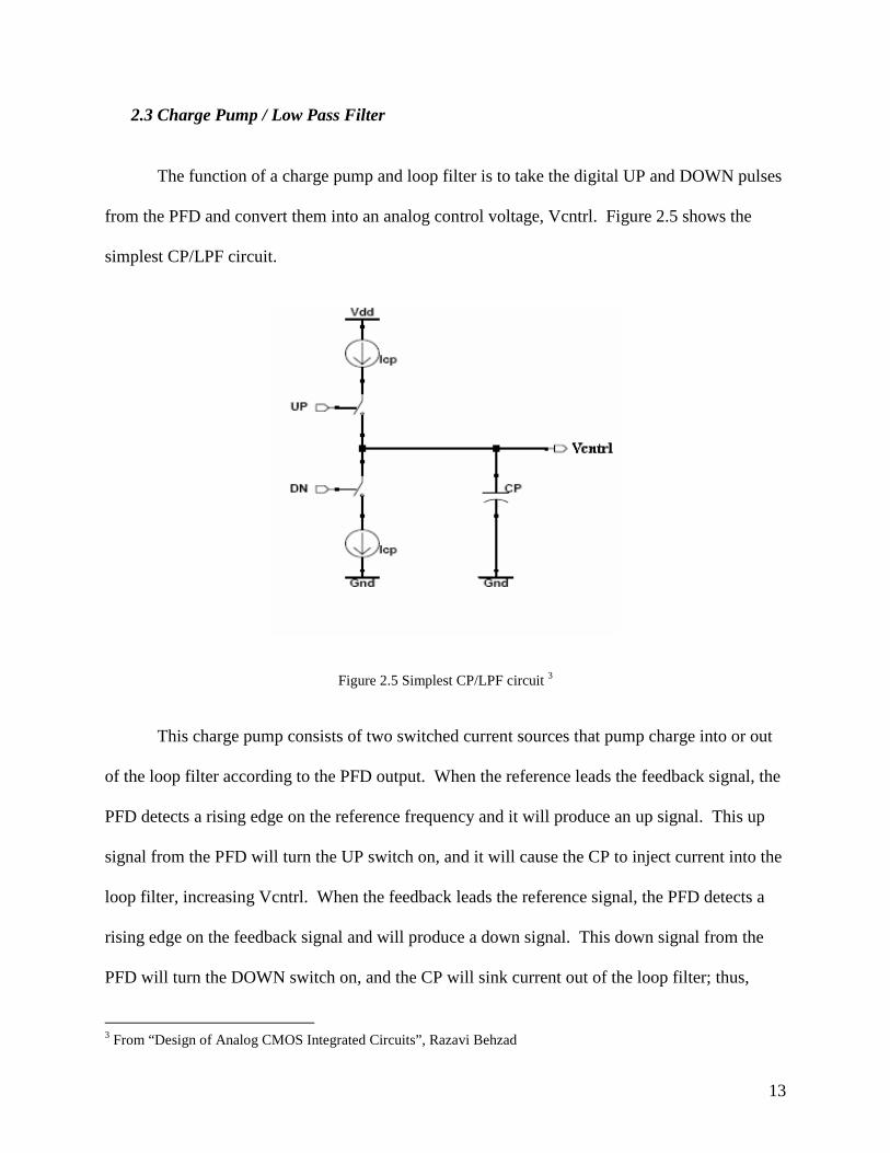
2.3 Charge Pump / Low Pass Filter
The function of a charge pump and loop filter is to take the digital UP and DOWN pulses
from the PFD and convert them into an analog control voltage, Vcntrl. Figure 2.5 shows the
simplest CP/LPF circuit.
Figure 2.5 Simplest CP/LPF circuit 3
This charge pump consists of two switched current sources that pump charge into or out
of the loop filter according to the PFD output. When the reference leads the feedback signal, the
PFD detects a rising edge on the reference frequency and it will produce an up signal. This up
signal from the PFD will turn the UP switch on, and it will cause the CP to inject current into the
loop filter, increasing Vcntrl. When the feedback leads the reference signal, the PFD detects a
rising edge on the feedback signal and will produce a down signal. This down signal from the
PFD will turn the DOWN switch on, and the CP will sink current out of the loop filter; thus,
3 From “Design of Analog CMOS Integrated Circuits”, Razavi Behzad
14
decreasing Vcntrl. The current through the UP switch, Iup, and the current through the down
switch, Idown , need to be equal in order to avoid any current mismatch. The minimum charge
pump current is limited by the switching speed requirements.
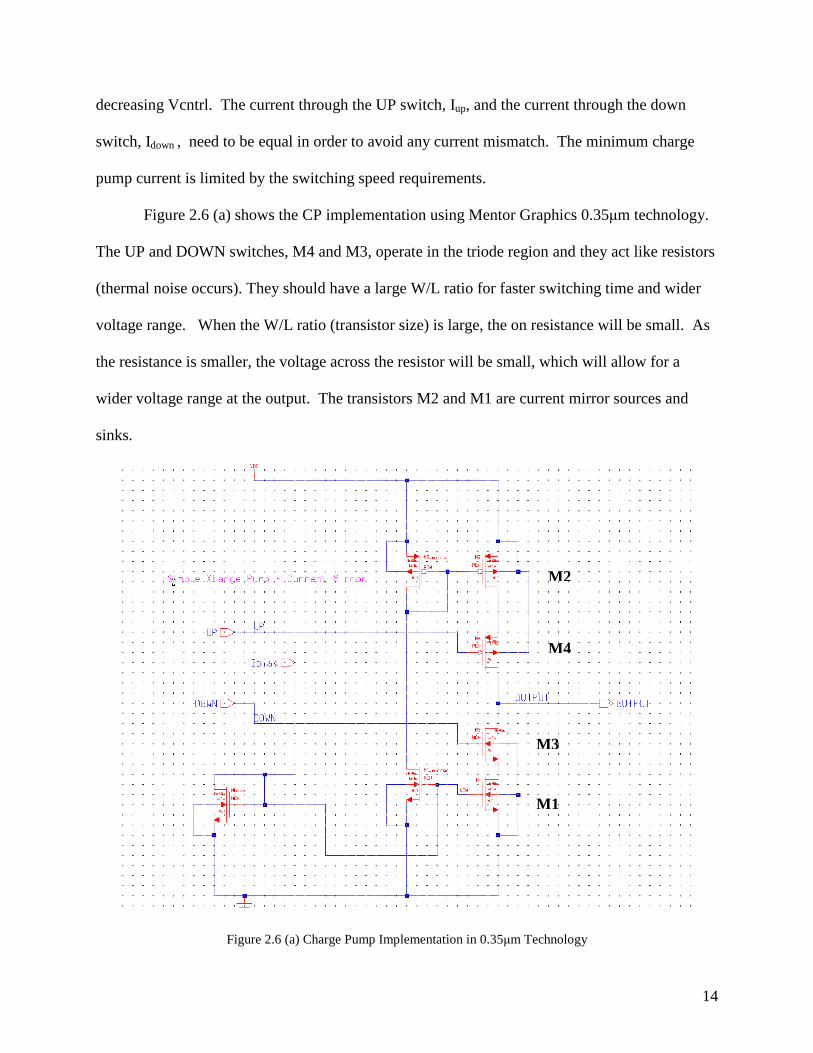
Figure 2.6 (a) shows the CP implementation using Mentor Graphics 0.35µm technology.
The UP and DOWN switches, M4 and M3, operate in the triode region and they act like resistors
(thermal noise occurs). They should have a large W/L ratio for faster switching time and wider
voltage range. When the W/L ratio (transistor size) is large, the on resistance will be small. As
the resistance is smaller, the voltage across the resistor will be small, which will allow for a
wider voltage range at the output. The transistors M2 and M1 are current mirror sources and
sinks.
Figure 2.6 (a) Charge Pump Implementation in 0.35µm Technology
M2
M1
M4
M3
15
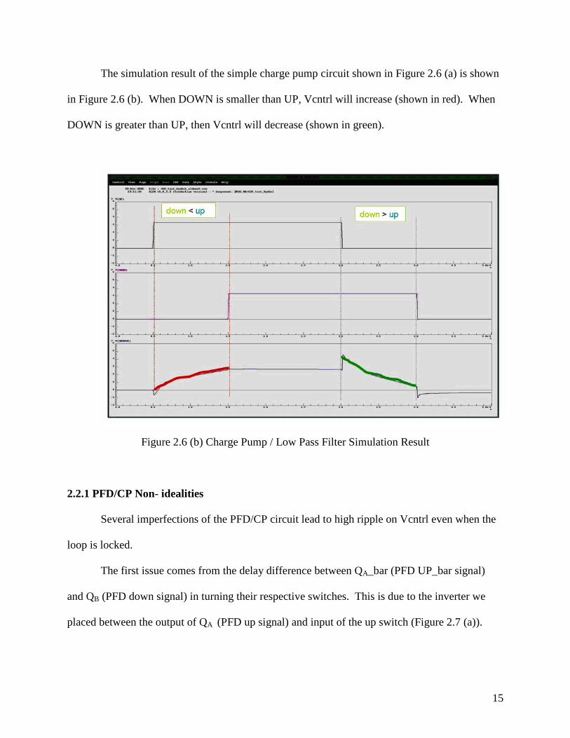
The simulation result of the simple charge pump circuit shown in Figure 2.6 (a) is shown
in Figure 2.6 (b). When DOWN is smaller than UP, Vcntrl will increase (shown in red). When
DOWN is greater than UP, then Vcntrl will decrease (shown in green).
Figure 2.6 (b) Charge Pump / Low Pass Filter Simulation Result
2.2.1 PFD/CP Non- idealities
Several imperfections of the PFD/CP circuit lead to high ripple on Vcntrl even when the
loop is locked.
The first issue comes from the delay difference between QA_bar (PFD UP_bar signal)
and QB (PFD down signal) in turning their respective switches. This is due to the inverter we
placed between the output of QA (PFD up signal) and input of the up switch (Figure 2.7 (a)).
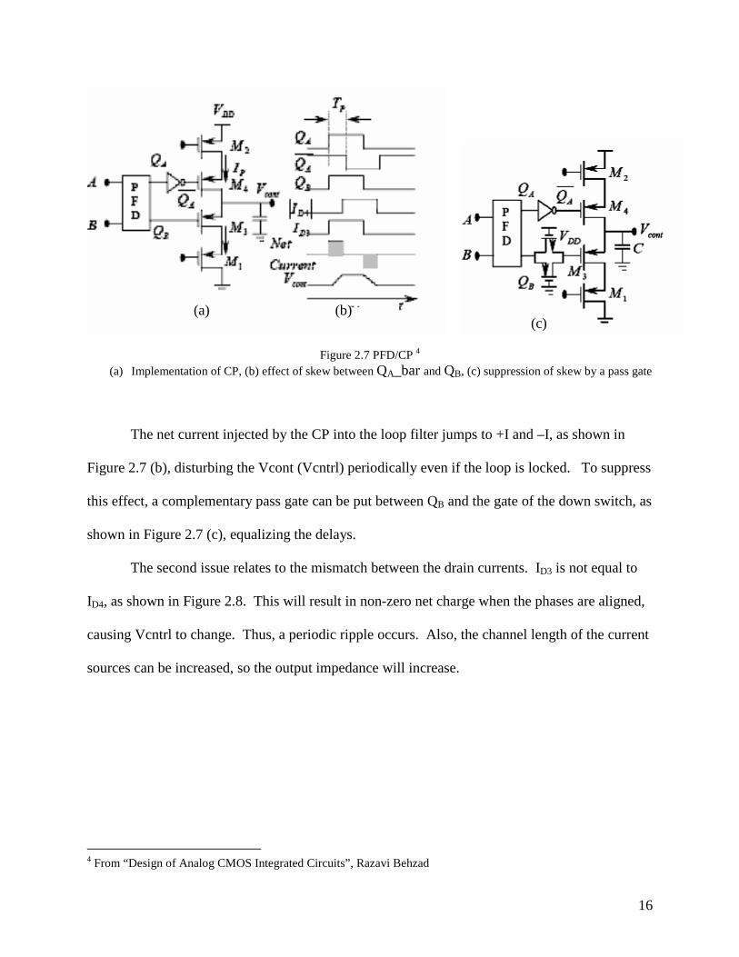
16
Figure 2.7 PFD/CP 4 (a) Implementation of CP, (b) effect of skew between QA_bar and QB, (c) suppression of skew by a pass gate
The net current injected by the CP into the loop filter jumps to +I and –I, as shown in
Figure 2.7 (b), disturbing the Vcont (Vcntrl) periodically even if the loop is locked. To suppress
this effect, a complementary pass gate can be put between QB and the gate of the down switch, as
shown in Figure 2.7 (c), equalizing the delays.
The second issue relates to the mismatch between the drain currents. ID3 is not equal to
ID4, as shown in Figure 2.8. This will result in non-zero net charge when the phases are aligned,
causing Vcntrl to change. Thus, a periodic ripple occurs. Also, the channel length of the current
sources can be increased, so the output impedance will increase.
4 From “Design of Analog CMOS Integrated Circuits”, Razavi Behzad
(a) (b) (c)
17
Figure 2.8 Charge Pump Current Mismatch 5
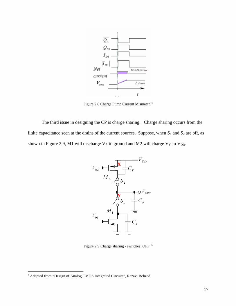
The third issue in designing the CP is charge sharing. Charge sharing occurs from the
finite capacitance seen at the drains of the current sources. Suppose, when S1 and S2 are off, as
shown in Figure 2.9, M1 will discharge Vx to ground and M2 will charge VY to VDD.
Figure 2.9 Charge sharing - switches: OFF 5
5 Adapted from “Design of Analog CMOS Integrated Circuits”, Razavi Behzad
X
Y
18
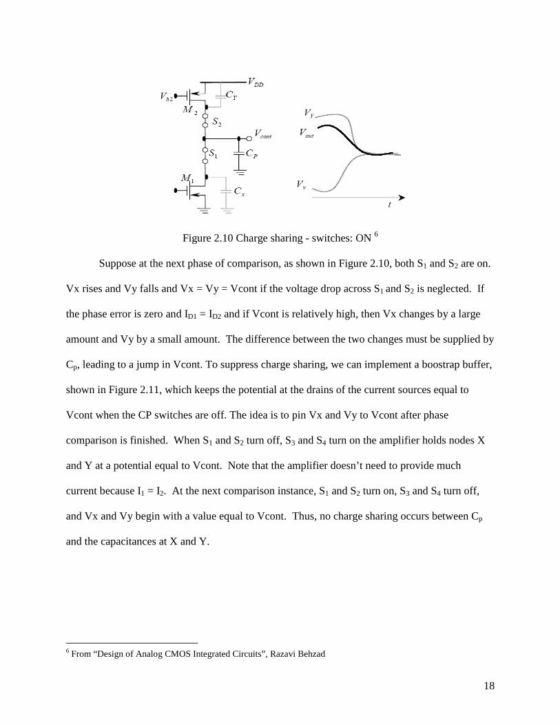
Figure 2.10 Charge sharing - switches: ON 6
Suppose at the next phase of comparison, as shown in Figure 2.10, both S1 and S2 are on.
Vx rises and Vy falls and Vx = Vy = Vcont if the voltage drop across S1 and S2 is neglected. If
the phase error is zero and ID1 = ID2 and if Vcont is relatively high, then Vx changes by a large
amount and Vy by a small amount. The difference between the two changes must be supplied by
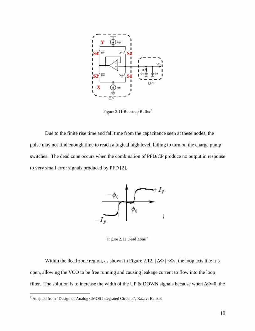
Cp, leading to a jump in Vcont. To suppress charge sharing, we can implement a boostrap buffer,
shown in Figure 2.11, which keeps the potential at the drains of the current sources equal to
Vcont when the CP switches are off. The idea is to pin Vx and Vy to Vcont after phase
comparison is finished. When S1 and S2 turn off, S3 and S4 turn on the amplifier holds nodes X
and Y at a potential equal to Vcont. Note that the amplifier doesn’t need to provide much
current because I1 = I2. At the next comparison instance, S1 and S2 turn on, S3 and S4 turn off,
and Vx and Vy begin with a value equal to Vcont. Thus, no charge sharing occurs between Cp
and the capacitances at X and Y.
6 From “Design of Analog CMOS Integrated Circuits”, Razavi Behzad
19
Figure 2.11 Boostrap Buffer7
Due to the finite rise time and fall time from the capacitance seen at these nodes, the
pulse may not find enough time to reach a logical high level, failing to turn on the charge pump
switches. The dead zone occurs when the combination of PFD/CP produce no output in response
to very small error signals produced by PFD [2].
Figure 2.12 Dead Zone 7
Within the dead zone region, as shown in Figure 2.12, | ∆Φ | <Φo, the loop acts like it’s
open, allowing the VCO to be free running and causing leakage current to flow into the loop
filter. The solution is to increase the width of the UP & DOWN signals because when ∆Φ=0, the
7 Adapted from “Design of Analog CMOS Integrated Circuits”, Razavi Behzad
S1
S2 S4
S3
X
Y
20
pulses always turn on the charge pump if they are sufficiently wide. One solution is to add a
delay into the reset path of the PFD.
Fig 3.18 (a) Improved Charge Pump Design Using .35u Technology
Fig 3.18 (a) Improved Charge Pump Design Using .35u Technology
Fig 3.18 (a) Improved Charge Pump Design Using .35u Technology
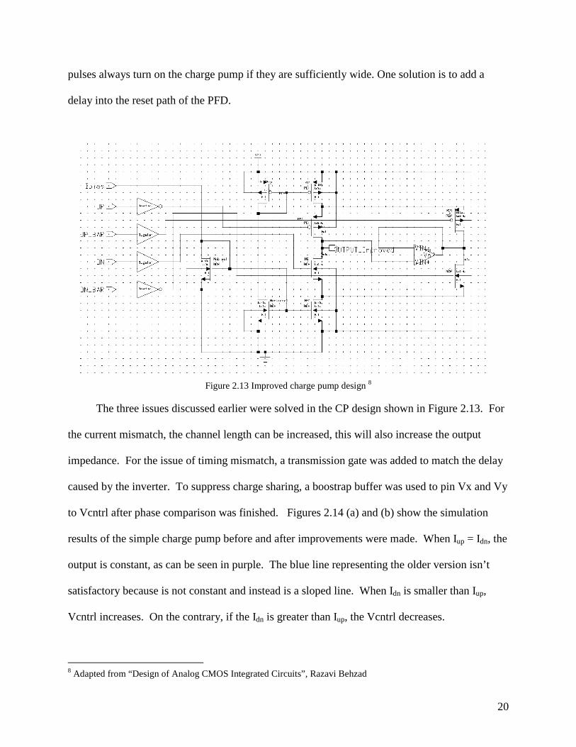
Figure 2.13 Improved charge pump design 8
The three issues discussed earlier were solved in the CP design shown in Figure 2.13. For
the current mismatch, the channel length can be increased, this will also increase the output
impedance. For the issue of timing mismatch, a transmission gate was added to match the delay
caused by the inverter. To suppress charge sharing, a boostrap buffer was used to pin Vx and Vy
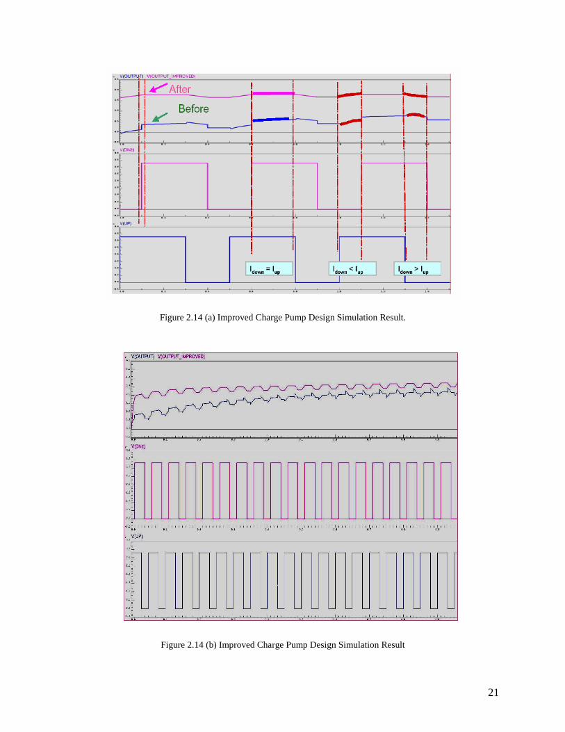
to Vcntrl after phase comparison was finished. Figures 2.14 (a) and (b) show the simulation
results of the simple charge pump before and after improvements were made. When Iup = Idn, the
output is constant, as can be seen in purple. The blue line representing the older version isn’t
satisfactory because is not constant and instead is a sloped line. When Idn is smaller than Iup,
Vcntrl increases. On the contrary, if the Idn is greater than Iup, the Vcntrl decreases.
8 Adapted from “Design of Analog CMOS Integrated Circuits”, Razavi Behzad
21
Figure 2.14 (a) Improved Charge Pump Design Simulation Result.
Figure 2.14 (b) Improved Charge Pump Design Simulation Result
A
B Z
22
2.4 Voltage Controlled Oscillator
The purpose of the VCO is to vary an output frequency proportional to the Vcntrl input.
2.4.1 VCO Architectures
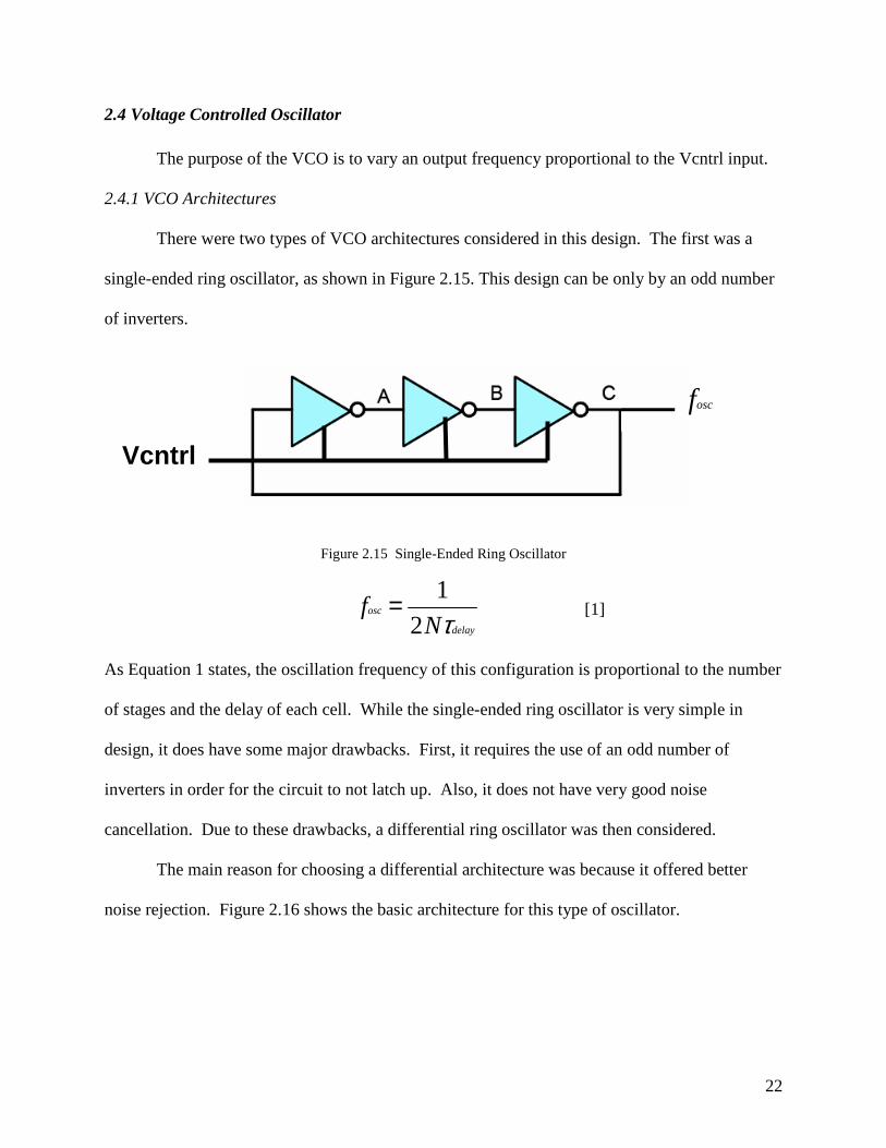
There were two types of VCO architectures considered in this design. The first was a
single-ended ring oscillator, as shown in Figure 2.15. This design can be only by an odd number
of inverters.
Figure 2.15 Single-Ended Ring Oscillator
[1]
As Equation 1 states, the oscillation frequency of this configuration is proportional to the number
of stages and the delay of each cell. While the single-ended ring oscillator is very simple in
design, it does have some major drawbacks. First, it requires the use of an odd number of
inverters in order for the circuit to not latch up. Also, it does not have very good noise
cancellation. Due to these drawbacks, a differential ring oscillator was then considered.
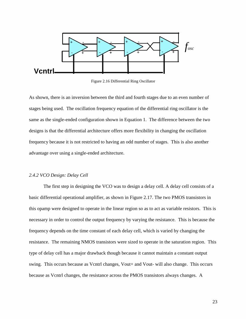
The main reason for choosing a differential architecture was because it offered better
noise rejection. Figure 2.16 shows the basic architecture for this type of oscillator.
oscf
Vcntrl
delay
osc
Nf
τ2
1=
23
Figure 2.16 Differential Ring Oscillator
As shown, there is an inversion between the third and fourth stages due to an even number of
stages being used. The oscillation frequency equation of the differential ring oscillator is the
same as the single-ended configuration shown in Equation 1. The difference between the two
designs is that the differential architecture offers more flexibility in changing the oscillation
frequency because it is not restricted to having an odd number of stages. This is also another
advantage over using a single-ended architecture.
2.4.2 VCO Design: Delay Cell
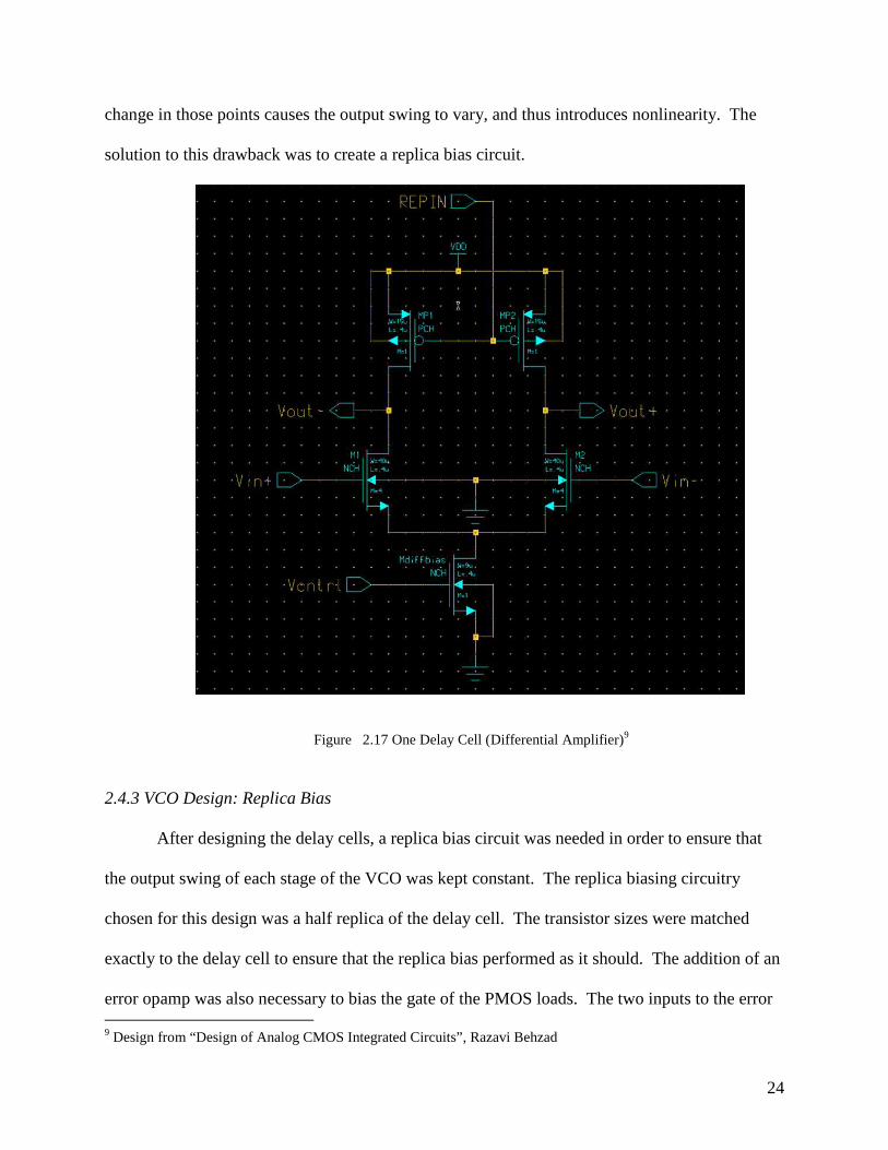
The first step in designing the VCO was to design a delay cell. A delay cell consists of a
basic differential operational amplifier, as shown in Figure 2.17. The two PMOS transistors in
this opamp were designed to operate in the linear region so as to act as variable resistors. This is
necessary in order to control the output frequency by varying the resistance. This is because the
frequency depends on the time constant of each delay cell, which is varied by changing the
resistance. The remaining NMOS transistors were sized to operate in the saturation region. This
type of delay cell has a major drawback though because it cannot maintain a constant output
swing. This occurs because as Vcntrl changes, Vout+ and Vout- will also change. This occurs
because as Vcntrl changes, the resistance across the PMOS transistors always changes. A
Vcntrl
oscf
24
change in those points causes the output swing to vary, and thus introduces nonlinearity. The
solution to this drawback was to create a replica bias circuit.
Figure 2.17 One Delay Cell (Differential Amplifier)9
2.4.3 VCO Design: Replica Bias
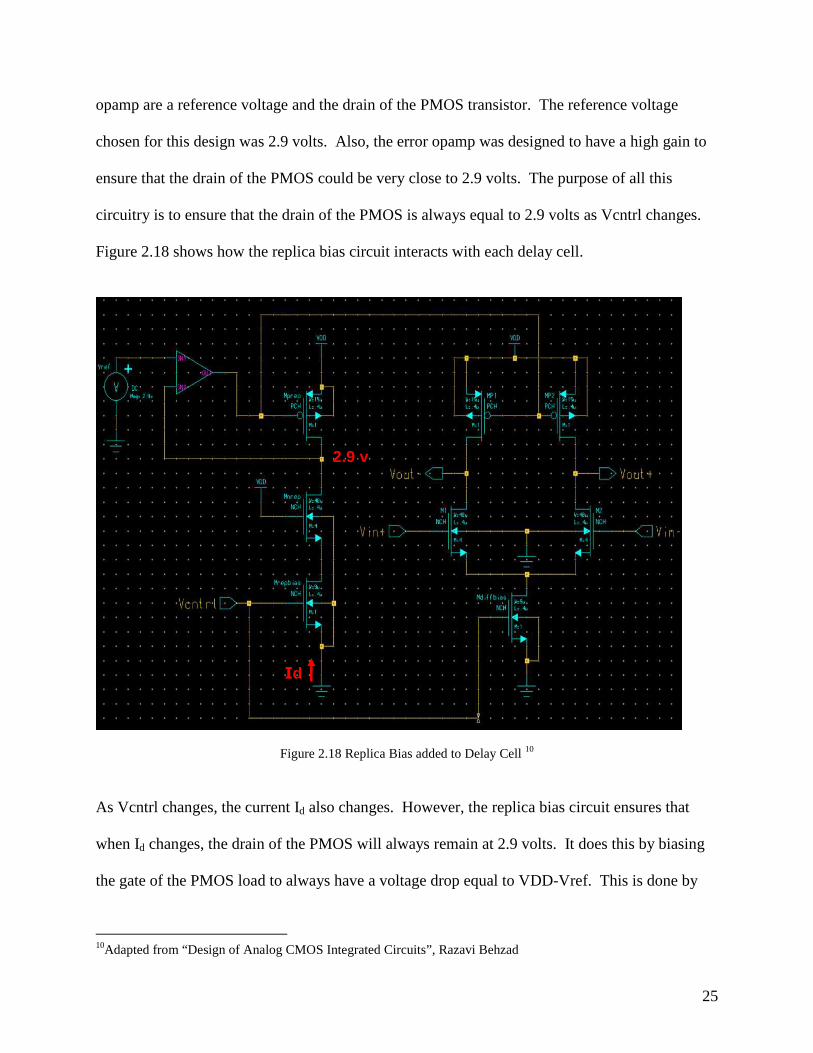
After designing the delay cells, a replica bias circuit was needed in order to ensure that
the output swing of each stage of the VCO was kept constant. The replica biasing circuitry
chosen for this design was a half replica of the delay cell. The transistor sizes were matched
exactly to the delay cell to ensure that the replica bias performed as it should. The addition of an
error opamp was also necessary to bias the gate of the PMOS loads. The two inputs to the error 9 Design from “Design of Analog CMOS Integrated Circuits”, Razavi Behzad
25
opamp are a reference voltage and the drain of the PMOS transistor. The reference voltage
chosen for this design was 2.9 volts. Also, the error opamp was designed to have a high gain to
ensure that the drain of the PMOS could be very close to 2.9 volts. The purpose of all this
circuitry is to ensure that the drain of the PMOS is always equal to 2.9 volts as Vcntrl changes.
Figure 2.18 shows how the replica bias circuit interacts with each delay cell.
Figure 2.18 Replica Bias added to Delay Cell 10
As Vcntrl changes, the current Id also changes. However, the replica bias circuit ensures that
when Id changes, the drain of the PMOS will always remain at 2.9 volts. It does this by biasing
the gate of the PMOS load to always have a voltage drop equal to VDD-Vref. This is done by
10Adapted from “Design of Analog CMOS Integrated Circuits”, Razavi Behzad
2.9 v
Id
26
varying the resistance of the PMOS load, which is equal to [(VDD – Vref)/Id]. Thus, in order to
maintain a constant voltage drop of VDD-Vref across the PMOS load, the resistance value has to
change according to Vcntrl. Furthermore, while the differential opamp undergoes full switching,
the replica bias will exactly match the delay cell, and thus enable the VCO to have a constant
swing.
2.4.4 VCO Design: Transistor Sizing
As mentioned before, the PMOS transistors were sized in order to operate as variable
resistors in the linear region while the NMOS transistors were all designed to operate in the
saturation region. Equations 2 and 3 show how the transistor sizing can affect the oscillation
frequency of the VCO.
[2] [2] [3] Changing the transistor sizes can affect the overall capacitance in each delay cell. Also the
oscillation frequency can be changed by changing ‘N,’ which is the number of stages in the
VCO. For the purposes of this design, four stages were used.
2.4.5 VCO Design: Differential to Single-Ended Converter
The next step was to design a differential to single-ended converter in order to create a
single-ended rail-to-rail output. This would give the output of the VCO a pulse going from 0 to
3.3 volts (Note: VDD = 3.3v). The first step in designing the converter was to implement a
totalop
osc
CRRNf
on )||(2
1=
inl CCC outtota +=
27
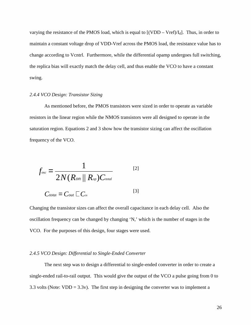
comparator. This comparator would have to shift the output swing from the last stage of the
delay cell (2.9-3.3 volts) down to a common mode of about 1.65 volts. This is necessary so the
signal can go through an inverter and properly output a discrete rail to rail signal. Figure 2.19
illustrates the configuration used for the comparator.
Figure 2.19 Comparator Design
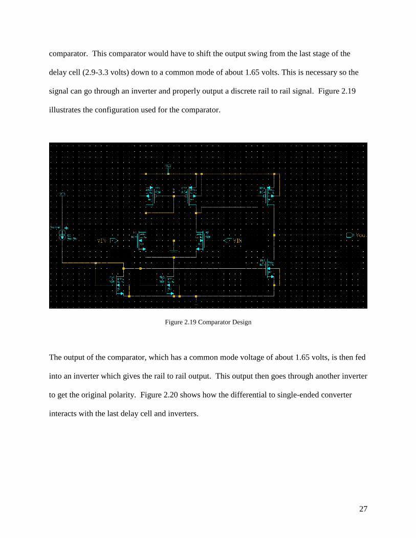
The output of the comparator, which has a common mode voltage of about 1.65 volts, is then fed
into an inverter which gives the rail to rail output. This output then goes through another inverter
to get the original polarity. Figure 2.20 shows how the differential to single-ended converter
interacts with the last delay cell and inverters.
28
Figure 2.20 Comparator interaction with delay cell and inverters
The next issue to consider was the fact that the output of the last delay cell was connected
to the comparator. This introduced extra capacitance to the last delay cell and thus made the four
delay cells asymmetrical. In order to make all of the delay cells symmetrical, dummy cells had
to be added to the other three delay cells. These dummy cells contained the same amount of
capacitance as the input transistors of the comparator, thus giving all four stages the same load.
2.4.6 VCO Design: Characteristic Plot
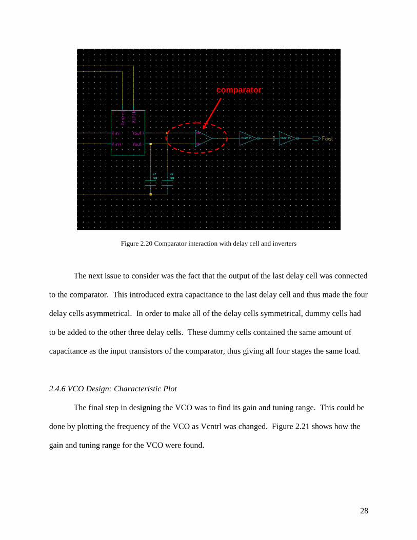
The final step in designing the VCO was to find its gain and tuning range. This could be
done by plotting the frequency of the VCO as Vcntrl was changed. Figure 2.21 shows how the
gain and tuning range for the VCO were found.
comparator
29
Vcontrol vs Frequency
0
100
200
300
400
500
600
700
800
900
0.67 0.
70.
80.
9 11.
05 1.1
1.15 1.
21.
25 1.3
1.35 1.
41.
45 1.5
1.55 1.
61.
71.
81.
9 22.
22.
3
Vcontrol (volts)
Fre
qu
ency
(M
Hz)
Figure 2.21
The tuning range of the VCO (321-538 MHz) was found by looking at the most linear region of
the curve, which was from 1 to 1.4 volts. The slope of that line gave the gain of the VCO, Kvco,
which was 542.5 MHz/v.
2.5 Low Pass Filter and Transfer Function
The loop filter is a really important part of the PLL, as it affects and determines the loop
stability. It also provides the necessary control voltage that is required to adjust the frequency of
the VCO. Figure 2.22 shows the RC network, which includes a resistor in series with the filter
capacitor. Each time the charge pump drives the R and C1 combination, a current is injected into
the filter, and the control voltage experiences a jump. To suppress this effect, a second capacitor
V1=1v F1 = 321 MHz
V2=1.4v F2 = 538 MHz
Kvco= 542.5 MHz/v
30
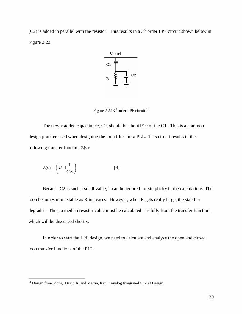
(C2) is added in parallel with the resistor. This results in a 3rd order LPF circuit shown below in
Figure 2.22.
Figure 2.22 3rd order LPF circuit 11
The newly added capacitance, C2, should be about1/10 of the C1. This is a common
design practice used when designing the loop filter for a PLL. This circuit results in the
following transfer function Z(s):
Z(s) =
+sC
R1
1 [4]
Because C2 is such a small value, it can be ignored for simplicity in the calculations. The
loop becomes more stable as R increases. However, when R gets really large, the stability
degrades. Thus, a median resistor value must be calculated carefully from the transfer function,
which will be discussed shortly.
In order to start the LPF design, we need to calculate and analyze the open and closed
loop transfer functions of the PLL.
11 Design from Johns, David A. and Martin, Ken “Analog Integrated Circuit Design
R C2
Vcntrl
C1
31
Acronyms used in the analysis:
Icp = charge pump current
Kvco=gain of the VCO (MHz/Volt)
Z(s) = loop filter transfer function
N = divider ratio (which will be further discussed shortly)
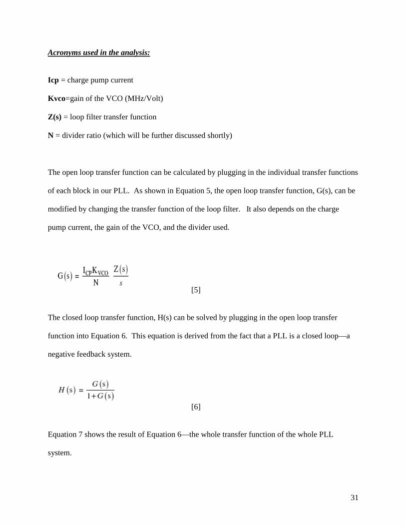
The open loop transfer function can be calculated by plugging in the individual transfer functions
of each block in our PLL. As shown in Equation 5, the open loop transfer function, G(s), can be
modified by changing the transfer function of the loop filter. It also depends on the charge
pump current, the gain of the VCO, and the divider used.
[5]
The closed loop transfer function, H(s) can be solved by plugging in the open loop transfer
function into Equation 6. This equation is derived from the fact that a PLL is a closed loop—a
negative feedback system.
[6]
Equation 7 shows the result of Equation 6—the whole transfer function of the whole PLL
system.
32
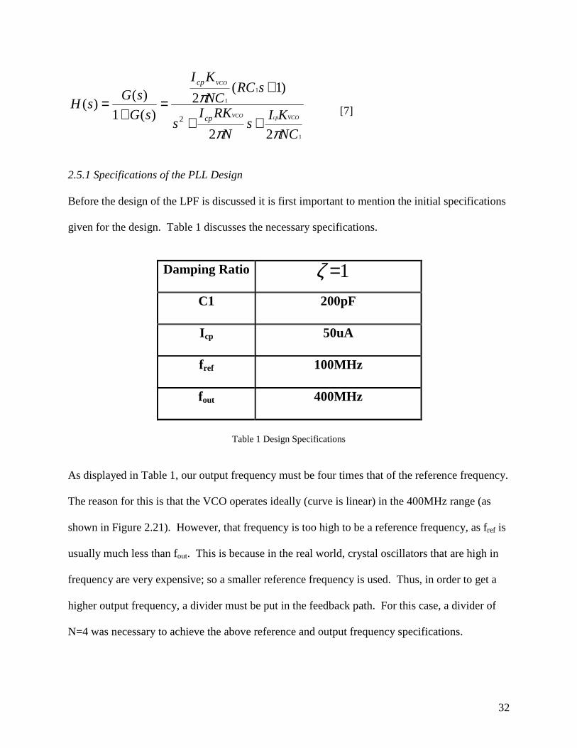
1
1
1
22
)1(2
)(1
)()(
2
NC
KIs
N
RKIs
sRCNC
KI
sG
sGsH
VCOcpVCO
VCO
cp
cp
ππ
π
++
+=
+= [7]
2.5.1 Specifications of the PLL Design
Before the design of the LPF is discussed it is first important to mention the initial specifications
given for the design. Table 1 discusses the necessary specifications.
Damping Ratio
C1 200pF
Icp 50uA
fref 100MHz
fout 400MHz
Table 1 Design Specifications
As displayed in Table 1, our output frequency must be four times that of the reference frequency.
The reason for this is that the VCO operates ideally (curve is linear) in the 400MHz range (as
shown in Figure 2.21). However, that frequency is too high to be a reference frequency, as fref is
usually much less than fout. This is because in the real world, crystal oscillators that are high in
frequency are very expensive; so a smaller reference frequency is used. Thus, in order to get a
higher output frequency, a divider must be put in the feedback path. For this case, a divider of
N=4 was necessary to achieve the above reference and output frequency specifications.
1=ζ
33
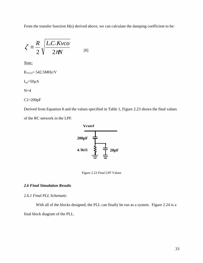
From the transfer function H(s) derived above, we can calculate the damping coefficient to be:
N
KvcoCIR cp
πζ
22
1= [8]
Note:
KVCO= 542.5MHz/V
Icp=50µA
N=4
C1=200pF
Derived from Equation 8 and the values specified in Table 1, Figure 2.23 shows the final values
of the RC network in the LPF.
Figure 2.23 Final LPF Values
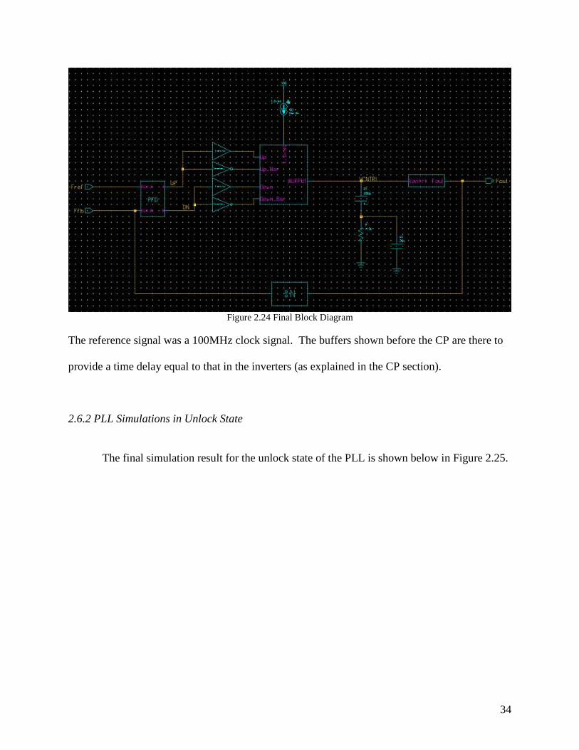
2.6 Final Simulation Results 2.6.1 Final PLL Schematic With all of the blocks designed, the PLL can finally be run as a system. Figure 2.24 is a
final block diagram of the PLL.
200pF
20pF
Vcntrl
4.3kΩ
34
Figure 2.24 Final Block Diagram
The reference signal was a 100MHz clock signal. The buffers shown before the CP are there to
provide a time delay equal to that in the inverters (as explained in the CP section).
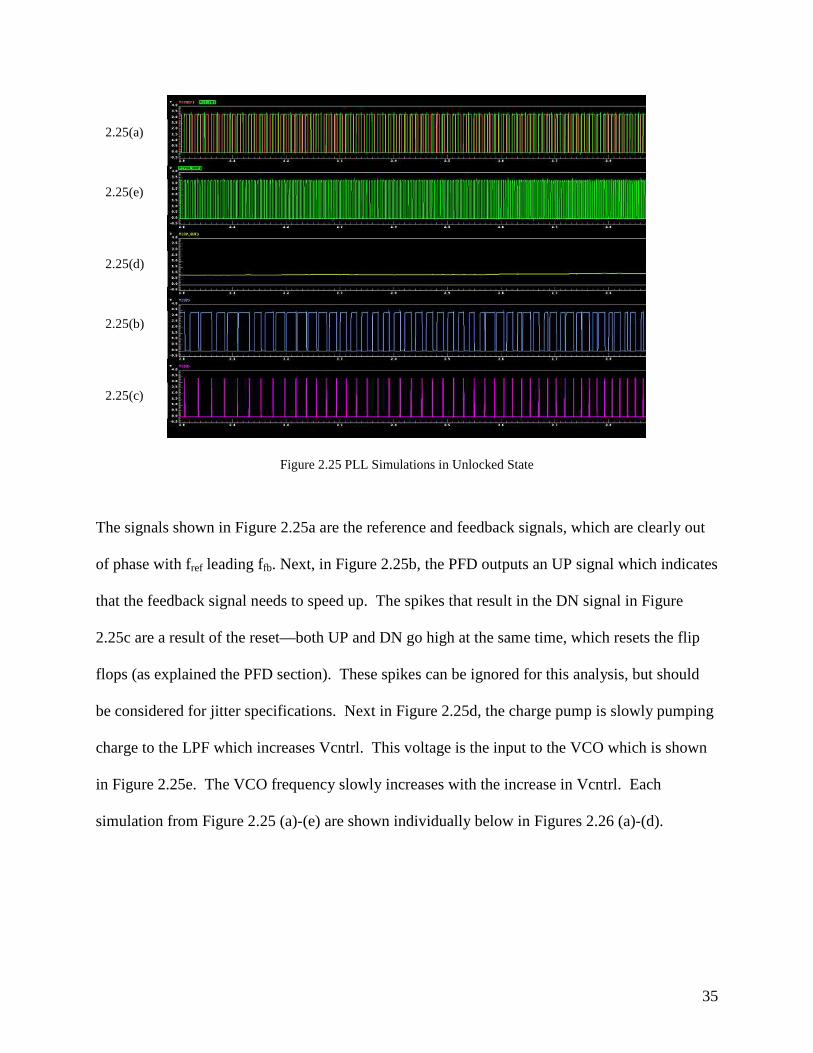
2.6.2 PLL Simulations in Unlock State The final simulation result for the unlock state of the PLL is shown below in Figure 2.25.
35
Figure 2.25 PLL Simulations in Unlocked State
The signals shown in Figure 2.25a are the reference and feedback signals, which are clearly out
of phase with fref leading ffb. Next, in Figure 2.25b, the PFD outputs an UP signal which indicates
that the feedback signal needs to speed up. The spikes that result in the DN signal in Figure
2.25c are a result of the reset—both UP and DN go high at the same time, which resets the flip
flops (as explained the PFD section). These spikes can be ignored for this analysis, but should
be considered for jitter specifications. Next in Figure 2.25d, the charge pump is slowly pumping
charge to the LPF which increases Vcntrl. This voltage is the input to the VCO which is shown
in Figure 2.25e. The VCO frequency slowly increases with the increase in Vcntrl. Each
simulation from Figure 2.25 (a)-(e) are shown individually below in Figures 2.26 (a)-(d).
2.25(b)
2.25(a)
2.25(d)
2.25(e)
2.25(c)
36
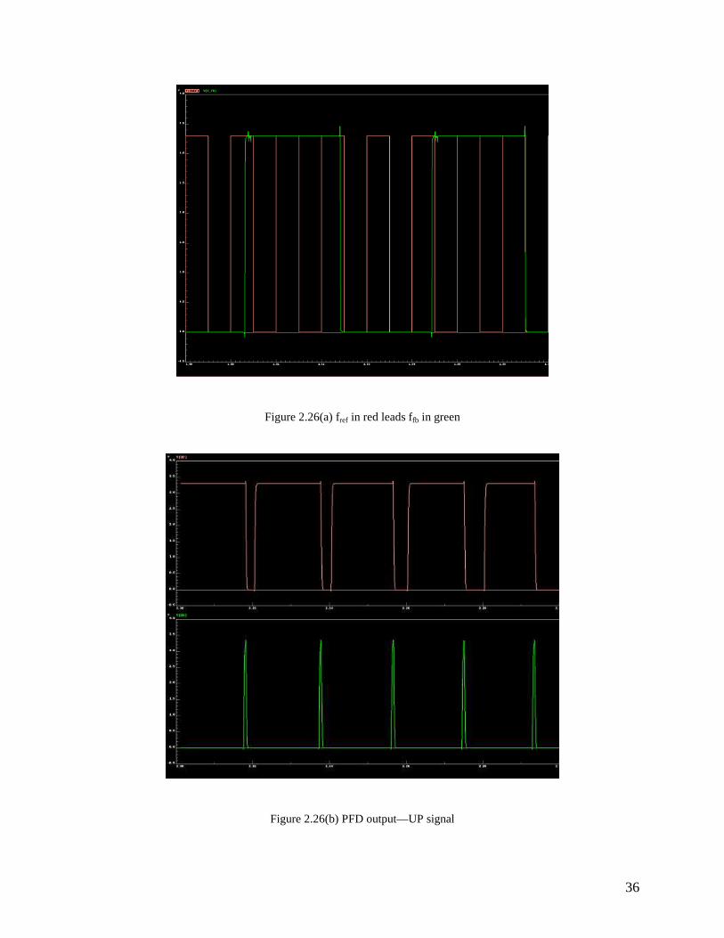
Figure 2.26(a) fref in red leads ffb in green
Figure 2.26(b) PFD output—UP signal
37
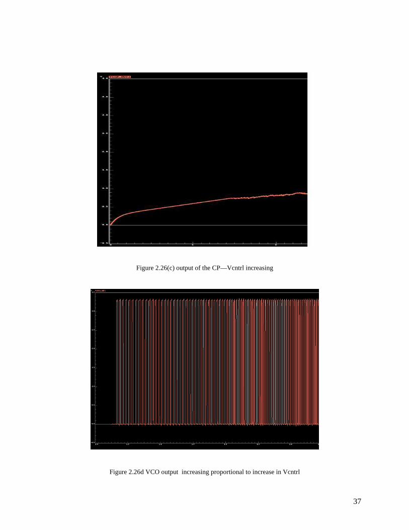
Figure 2.26(c) output of the CP—Vcntrl increasing
Figure 2.26d VCO output increasing proportional to increase in Vcntrl
38
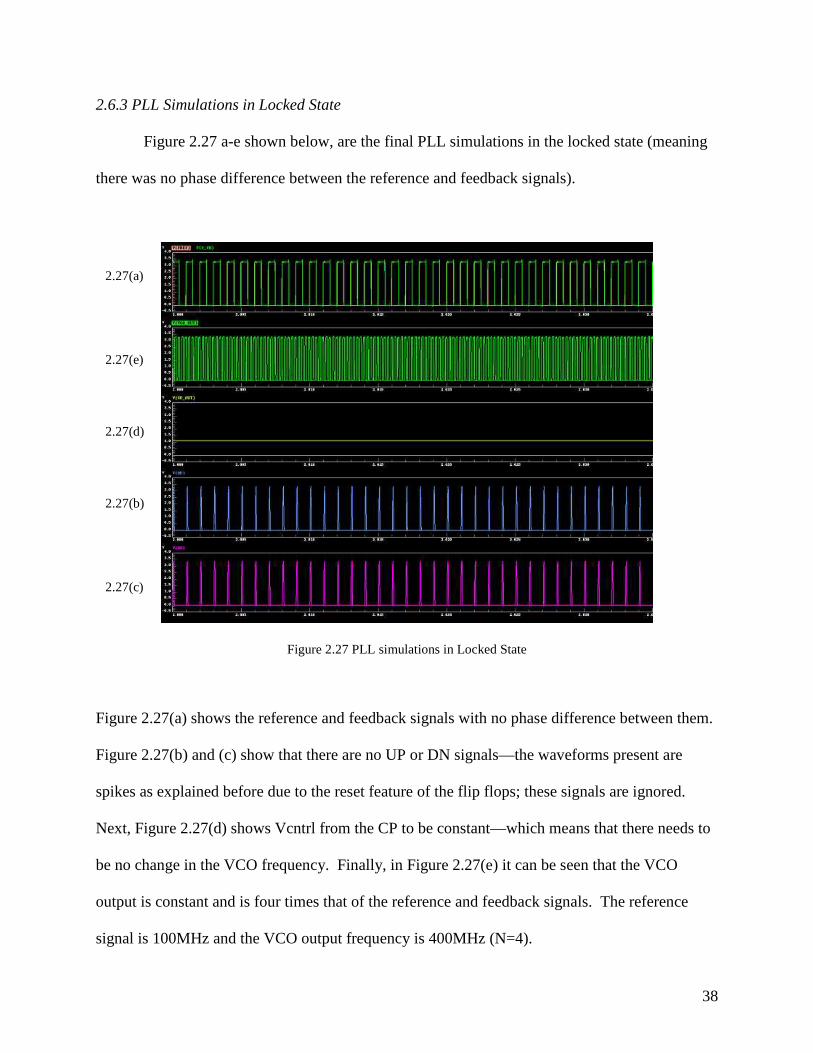
2.6.3 PLL Simulations in Locked State Figure 2.27 a-e shown below, are the final PLL simulations in the locked state (meaning
there was no phase difference between the reference and feedback signals).
Figure 2.27 PLL simulations in Locked State
Figure 2.27(a) shows the reference and feedback signals with no phase difference between them.
Figure 2.27(b) and (c) show that there are no UP or DN signals—the waveforms present are
spikes as explained before due to the reset feature of the flip flops; these signals are ignored.
Next, Figure 2.27(d) shows Vcntrl from the CP to be constant—which means that there needs to
be no change in the VCO frequency. Finally, in Figure 2.27(e) it can be seen that the VCO
output is constant and is four times that of the reference and feedback signals. The reference
signal is 100MHz and the VCO output frequency is 400MHz (N=4).
2.27(b)
2.27(a)
2.27(c)
2.27(d)
2.27(e)
39
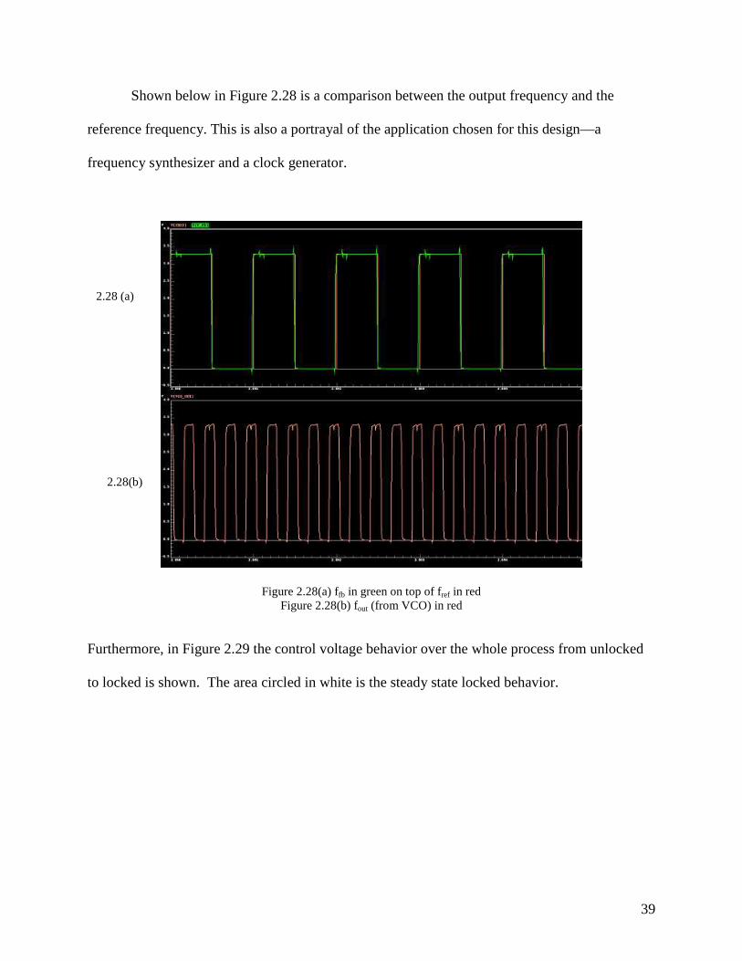
Shown below in Figure 2.28 is a comparison between the output frequency and the
reference frequency. This is also a portrayal of the application chosen for this design—a
frequency synthesizer and a clock generator.
Figure 2.28(a) ffb in green on top of fref in red Figure 2.28(b) fout (from VCO) in red
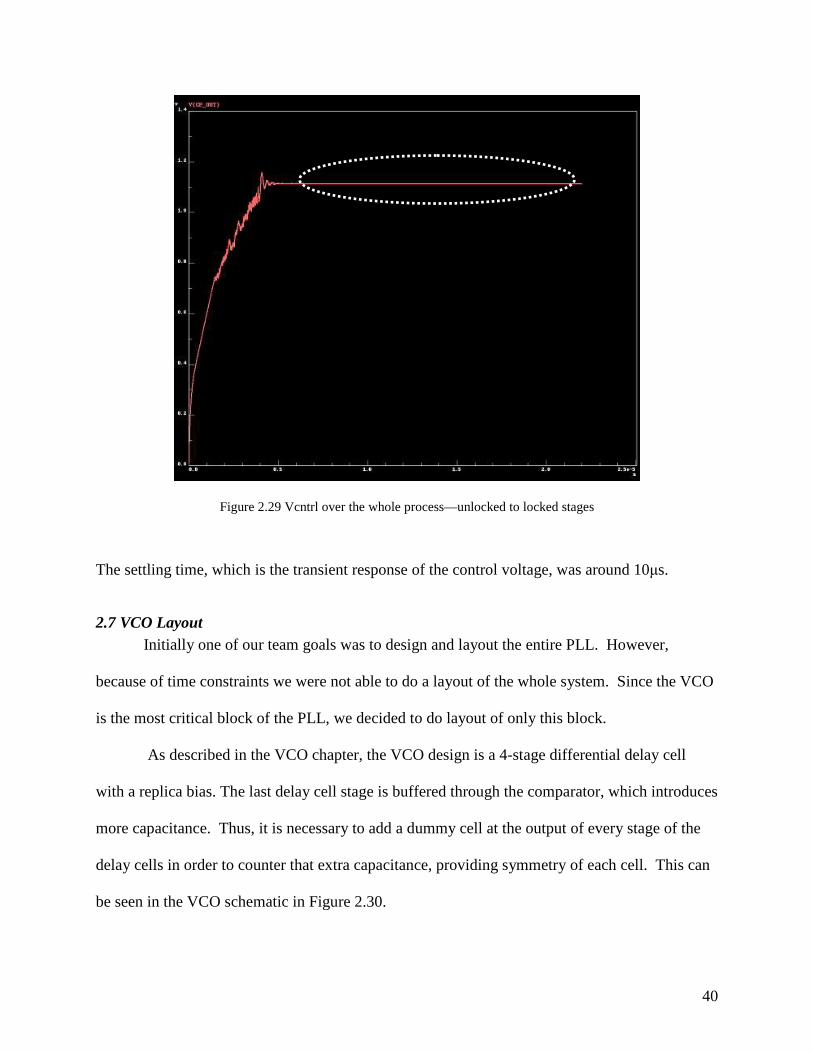
Furthermore, in Figure 2.29 the control voltage behavior over the whole process from unlocked
to locked is shown. The area circled in white is the steady state locked behavior.
2.28(b)
2.28 (a)
40
Figure 2.29 Vcntrl over the whole process—unlocked to locked stages
The settling time, which is the transient response of the control voltage, was around 10µs.
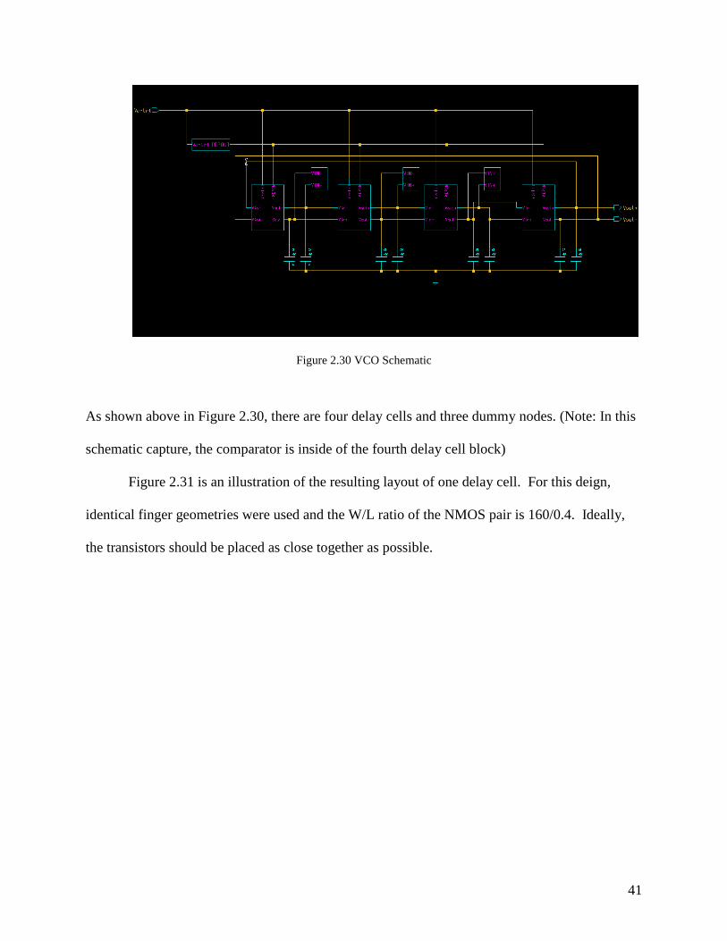
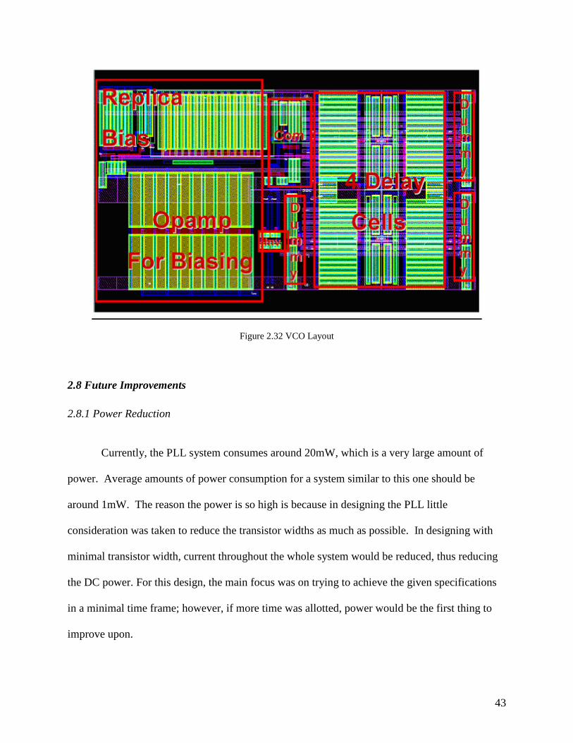
2.7 VCO Layout Initially one of our team goals was to design and layout the entire PLL. However,
because of time constraints we were not able to do a layout of the whole system. Since the VCO
is the most critical block of the PLL, we decided to do layout of only this block.
As described in the VCO chapter, the VCO design is a 4-stage differential delay cell
with a replica bias. The last delay cell stage is buffered through the comparator, which introduces
more capacitance. Thus, it is necessary to add a dummy cell at the output of every stage of the
delay cells in order to counter that extra capacitance, providing symmetry of each cell. This can
be seen in the VCO schematic in Figure 2.30.
41
Figure 2.30 VCO Schematic
As shown above in Figure 2.30, there are four delay cells and three dummy nodes. (Note: In this
schematic capture, the comparator is inside of the fourth delay cell block)
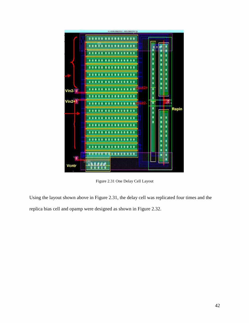
Figure 2.31 is an illustration of the resulting layout of one delay cell. For this deign,
identical finger geometries were used and the W/L ratio of the NMOS pair is 160/0.4. Ideally,
the transistors should be placed as close together as possible.
42
Figure 2.31 One Delay Cell Layout
Using the layout shown above in Figure 2.31, the delay cell was replicated four times and the
replica bias cell and opamp were designed as shown in Figure 2.32.
43
Figure 2.32 VCO Layout
2.8 Future Improvements
2.8.1 Power Reduction
Currently, the PLL system consumes around 20mW, which is a very large amount of
power. Average amounts of power consumption for a system similar to this one should be
around 1mW. The reason the power is so high is because in designing the PLL little
consideration was taken to reduce the transistor widths as much as possible. In designing with
minimal transistor width, current throughout the whole system would be reduced, thus reducing
the DC power. For this design, the main focus was on trying to achieve the given specifications
in a minimal time frame; however, if more time was allotted, power would be the first thing to
improve upon.
44
2.8.2Minimize Glitches in the Output
As shown in Figure 2.28 there are glitches in both the output and feedback signals. These
glitches can be a result of the comparator used at the last stage of the VCO delay cell. The
glitches might occur from some instability in the op-amp used in the comparator. Thus, if more
time was allotted, it would be optimal to design a more stable op-amp in the comparator.
2.8.3 Increase Bandwidth
Currently the BW of this PLL is around 1.16Mrad/s. Although this is much less than the
design practice of 1/10 of the reference frequency, it is ideal to have a BW as large as possible.
In increasing BW, the lock time will decrease, which will decrease power. However, the
tradeoff with an increase in BW is that the phase noise will increase. Thus, a middle range that
will give the highest BW with the least amount of phase noise as possible is ideal. Furthermore
to decrease the phase noise a different VCO design that does not incorporate resistances should
be considered.
3. Societal Issues
3.1 Engineering Standards and Constraints 3.1.1 Economic
From an economic standpoint our project is very cost effective. Budget constraints
would only apply in choosing test equipment for the PLL. Furthermore, the PLL is sometimes a
cheaper alternative to engineering solutions. For example, for clock synthesis quartzes are used
to generate certain clock frequencies. However, as the frequency increases so does the cost. So
it is cheaper to use lower frequency quartz and use a multiplier in the PLL to increase the quartz
frequency to avoid high costs.
45
3.1.2 Sustainability PLL’s are only sustainable in systems that don’t change with technology. However,
since there are very few of these systems, the PLL can also be unsustainable. Technology is
always updating and with newer technologies comes different approaches to building PLL’s. For
example, transistor lengths are continuing to decrease in size. This means that the sub-systems
within the PLL might have to be re-designed in accordance with the newer technologies.
3.1.3Manufacturability The PLL is not easy to manufacture. The PLL is made in an integrated circuit package
which means that due to constraints in size on wafers, manufacturability is extremely difficult.
This is why PLL’s must be sent out to fabrication labs to be manufactured—this process takes
three to six months.
3.1.4 Environmental
The environmental affects by the PLL are minimal. The PLL can serve as an alternative
to high frequency quartzes. Quartzes are natural resources and by using PLL’s we can reduce the
amount of this resource used.
3.1.5 Social PLL indirectly improves the quality of human life. PLL’s are used in a lot of electrical
engineering technologies. For example, the PLL is used in wireless communications. With
wireless communication, we are able to fly airplanes, send satellites into outer space, be able to
talk with each other on telephones from anywhere in the world. All of these applications use
PLL technology and without the PLL, humans wouldn’t be living in such an advanced society.
3.2 Cost Analysis
46
The cost associated with implementing and simulating an all software PLL system by
Mentor Graphics or other software is negligible in our case. In our design, all the functions of
the PLL are performed by using the Mentor Graphics software, which is readily available at the
Design Center at Santa Clara University for free. Software for PLL design offers freedom and it
is can be economically justified. However, we do recognize the simulation program does not
represent a real-time system. So, if we were to buy a board to test, the cost would be around
$150.00.
4. Conclusion PLL design is very hard work. Initially, we all knew that designing a PLL was going to be a
very challenging subject; however, when we actually started the design process the challenge
was bigger than we had anticipated. Since, PLL theory is usually not taught at the undergraduate
level, it was necessary to learn the theory on our own. With the help of our advisor and a few
good text books, we were able to learn all of the theory. However, we quickly learned that
design and theory are very different. We ran into issues during the design that we sometimes
couldn’t figure out using the theory in the text books. In order to solve this problem, we had to
seek outside help (advisor or people from industry) or we had to read technical papers that we
found through the IEEE website that explained such design practices.
Furthermore, our team learned a lot of teamwork skills. Since we initially split up the
work into blocks we had to learn to work together in putting all of the blocks together to create a
whole system. In doing so, we learned to adapt to each other’s work habits and we also had to
learn time management. It wasn’t easy working in a team but in the end, we learned to work
together and were able to finish the design.

47
Although the design process was long and extremely challenging, in the end we learned
very advanced concepts that are invaluable to take with us to industry. In designing a real-world
technology we learned design principles that are not taught in school—this knowledge is
extremely valuable. All of the hard work was worth the knowledge that we are able to walk away
with and furthermore, the hard work especially pays off when the design works. There is no
better feeling than that of getting your own design to work!
48
Works Cited
Behzad Razavi. “Design of Analog CMOS Integrated Circuits.” McGraw-Hall.
Johns, David A., Martin, Ken. “Analog Integrated Circuit Design.” John Wiley & Sons, Inc., 1997.
Kim, D Helman, P.R. Gray. “A 30-MHz Hybrid Analog/Digital Clock Recovery Circuit in 2µm CMOS,” IEEE Journal of Solid State Circuits, Vol. 25, No.6, pp.1385-1394, December 1990.
Leenaerts, J. van der Tang, C. Vaucher. “Circuit Design for RF Transceivers,” Boston: Kluwer Academic Publishers, 2001.
Maxim, Adrian. “Design Challenges In Multi-GHz PLL Frequency Synthesizers.” Silicon Laboratories. Accessed on 1 Dec. 2005. http://www.cerc.utexas.edu/msrf-seminar/y2005/tk050503_slides_maxim.pdf
Van Roon, Tony. “Phase Locked Loops”. 2001. Accessed on: 1 Dec. 2005. http://www.uoguelph.ca/~antoon/gadgets/pll/pll.html