Embed Size (px)
Citation preview
Phase Locked Loop
Ayman KhattabMohamed Saleh
Mostafa El-KhoulyTarek El-Rifai
Outline
• PLL Overview• Type (I) PLL
• Phase detector• Low Pass Filter• Voltage Controlled Oscillator
• Type (II) PLL• Phase/Frequency Detector• Charge Pump PLL
• Drawbacks of PLL • Applications
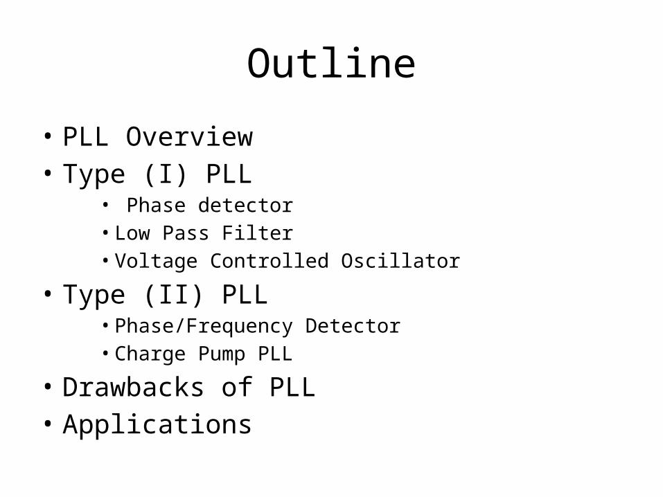
What is PLL ?!
• PLL is an electronic circuit that locks the phase of the output to the input.
Phase Locked LoopVin Vout
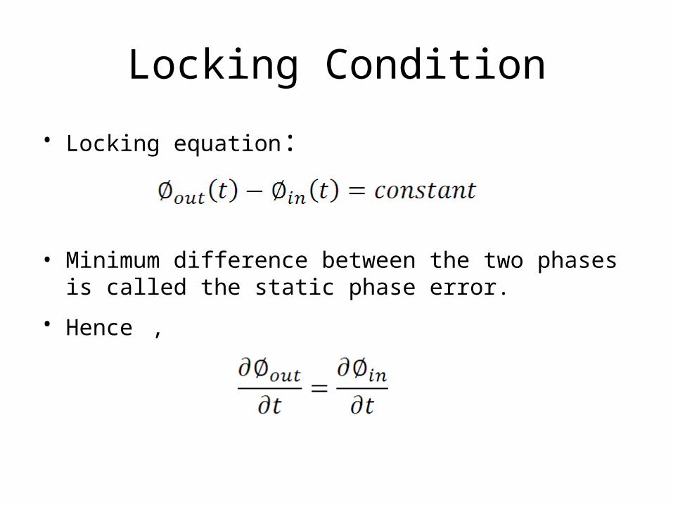
Locking Condition
• Locking equation:
• Minimum difference between the two phases is called the static phase error.
• Hence ,
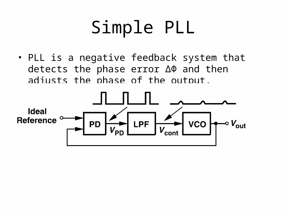
Simple PLL
• PLL is a negative feedback system that detects the phase error ΔΦ and then adjusts the phase of the output.
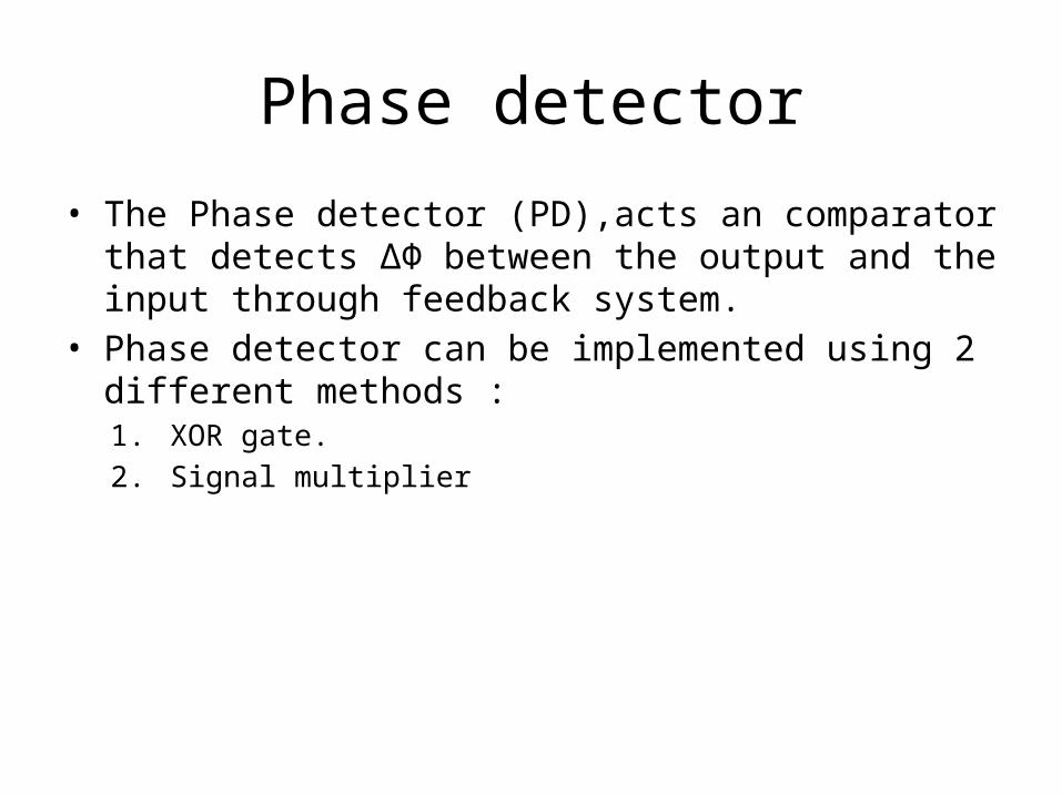
Phase detector
• The Phase detector (PD),acts an comparator that detects ΔΦ between the output and the input through feedback system.
• Phase detector can be implemented using 2 different methods : 1. XOR gate.2. Signal multiplier
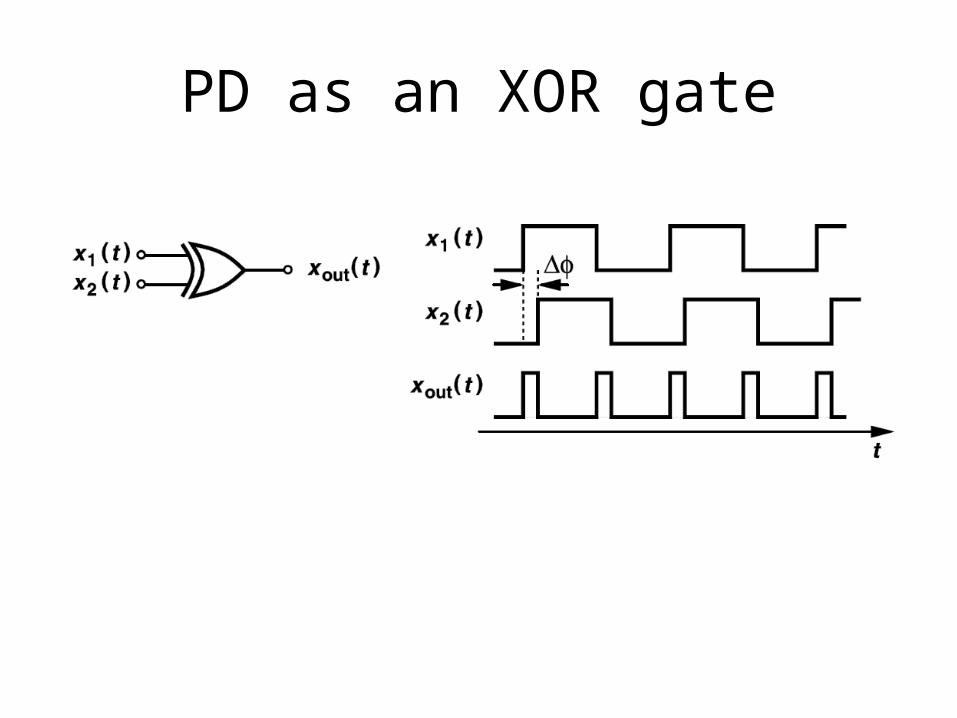
PD as an XOR gate
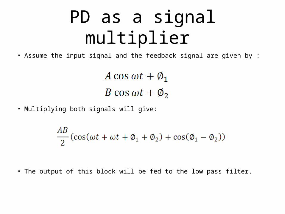
PD as a signal multiplier • Assume the input signal and the feedback signal are given by :
• Multiplying both signals will give:
• The output of this block will be fed to the low pass filter.
Low Pass Filter
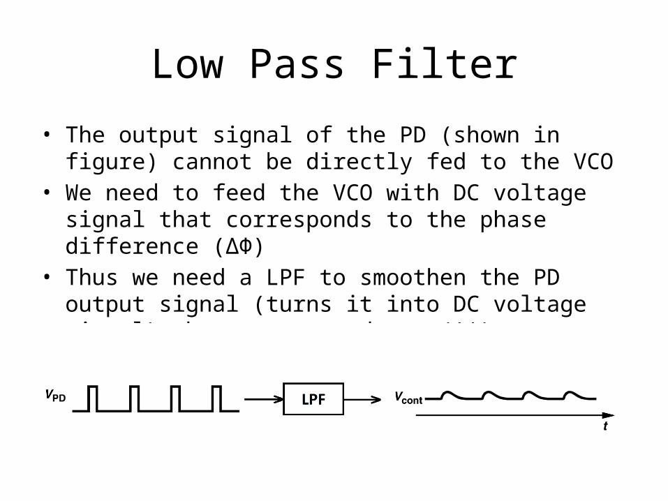
• The output signal of the PD (shown in figure) cannot be directly fed to the VCO
• We need to feed the VCO with DC voltage signal that corresponds to the phase difference (ΔΦ)
• Thus we need a LPF to smoothen the PD output signal (turns it into DC voltage signal) that corresponds to (ΔΦ)
LPF output
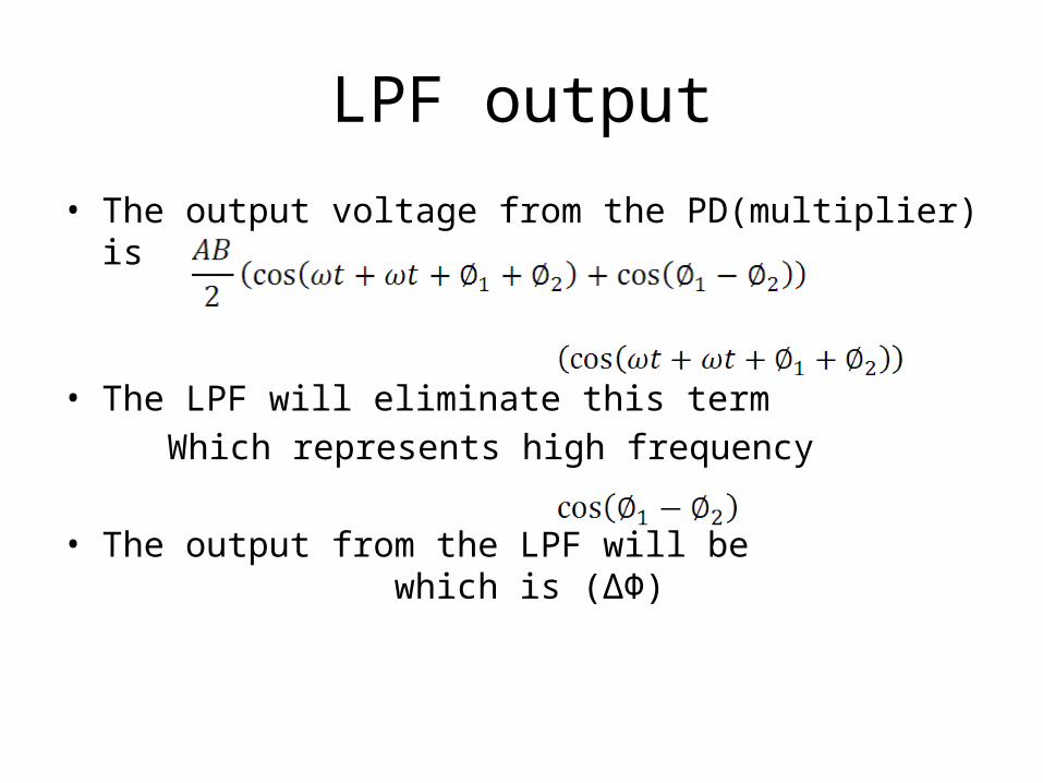
• The output voltage from the PD(multiplier) is
• The LPF will eliminate this term Which represents high frequency
• The output from the LPF will be which is (ΔΦ)
Voltage Controlled Oscillator
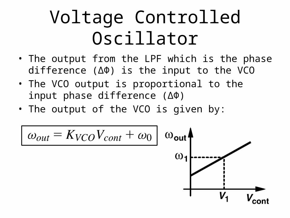
• The output from the LPF which is the phase difference (ΔΦ) is the input to the VCO
• The VCO output is proportional to the input phase difference (ΔΦ)
• The output of the VCO is given by:
Alignment of the VCO’s phase
• The VCO oscillates at the same frequency as an ideal reference but with a finite phase error.
• It is required to eliminate the phase error by adjusting the phase of the VCO.
• But the phase does not change instantaneously so the frequency of the VCO must be changed, allowing it to accumulate phase faster or slower than the reference eventually eliminating the phase error.
• After the phase is eliminated the frequency of the VCO is returned to its initial value.
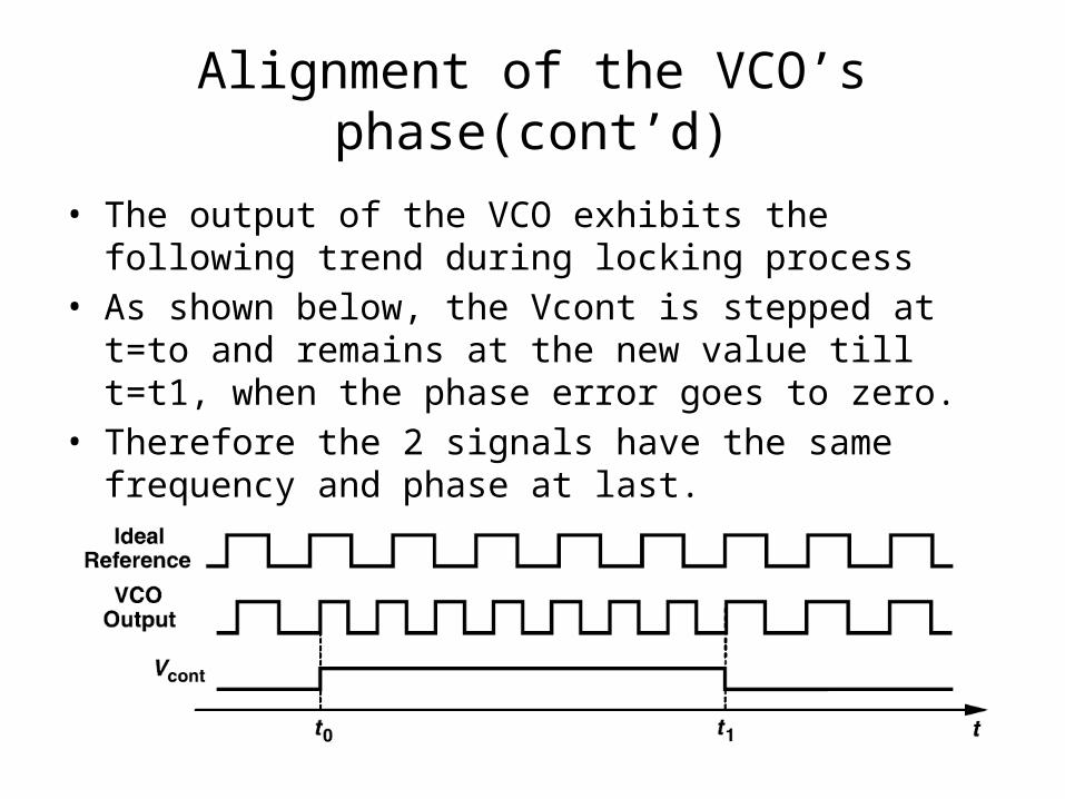
Alignment of the VCO’s phase(cont’d)
• The output of the VCO exhibits the following trend during locking process
• As shown below, the Vcont is stepped at t=to and remains at the new value till t=t1, when the phase error goes to zero.
• Therefore the 2 signals have the same frequency and phase at last.
Type(II) PLL
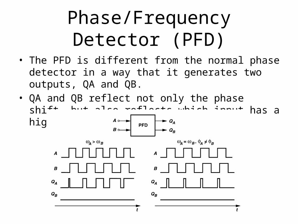
Phase/Frequency Detector (PFD)
• The PFD is different from the normal phase detector in a way that it generates two outputs, QA and QB.
• QA and QB reflect not only the phase shift, but also reflects which input has a higher frequency.
Phase/Frequency Detector (PFD)
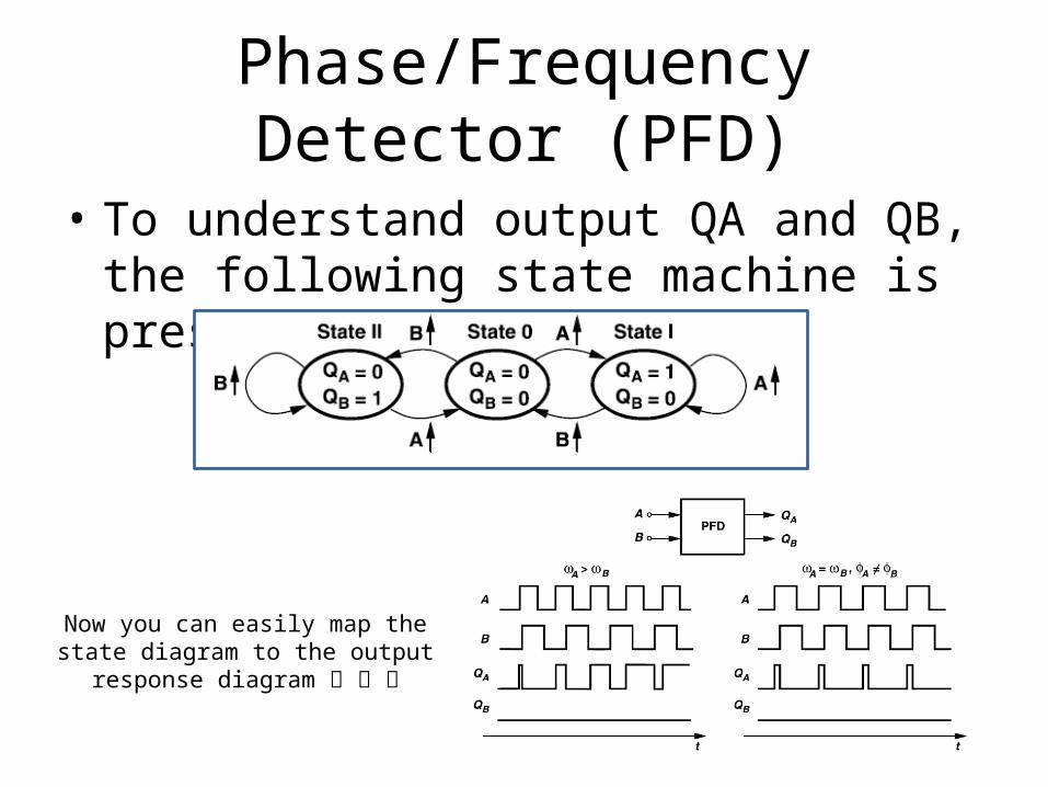
• To understand output QA and QB, the following state machine is presented
Now you can easily map the state diagram to the output response diagram
Phase/Frequency Detector (PFD)
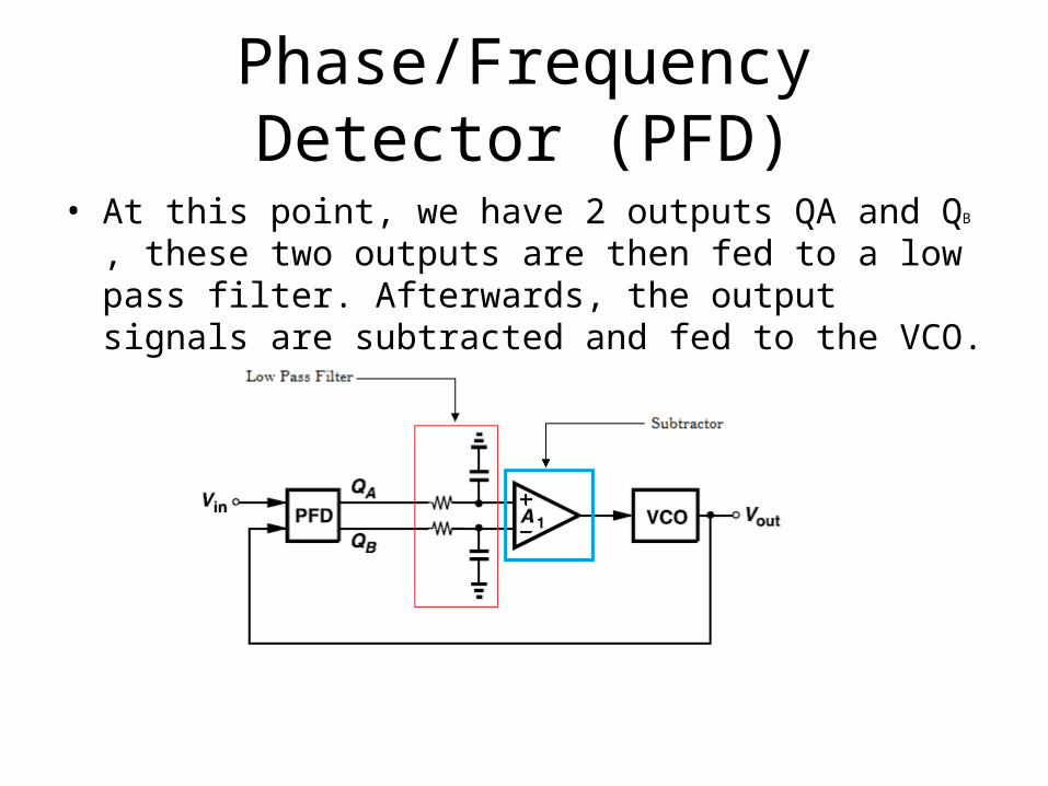
• At this point, we have 2 outputs QA and QB , these two outputs are then fed to a low pass filter. Afterwards, the output signals are subtracted and fed to the VCO.
Phase/Frequency Detector (PFD)
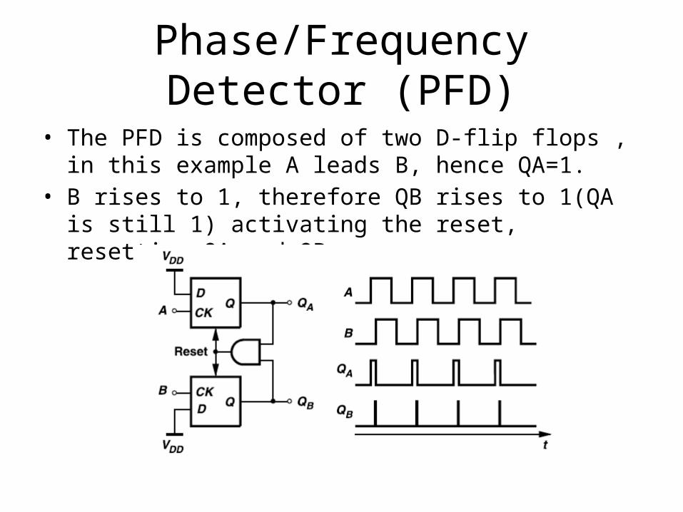
• The PFD is composed of two D-flip flops , in this example A leads B, hence QA=1.
• B rises to 1, therefore QB rises to 1(QA is still 1) activating the reset, resetting QA and QB.
PD vs. PFD
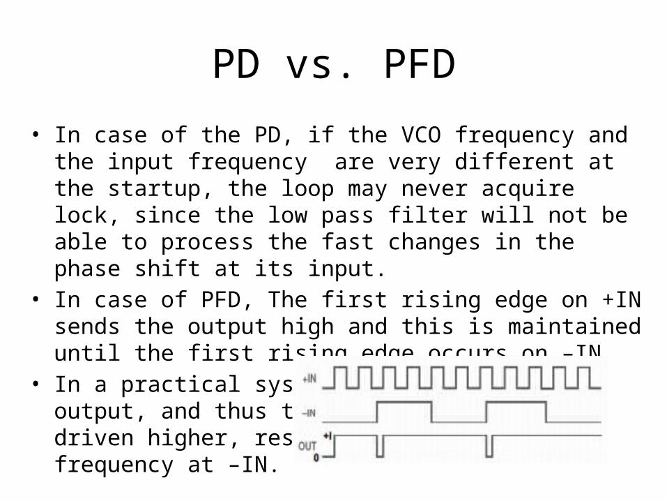
• In case of the PD, if the VCO frequency and the input frequency are very different at the startup, the loop may never acquire lock, since the low pass filter will not be able to process the fast changes in the phase shift at its input.
• In case of PFD, The first rising edge on +IN sends the output high and this is maintained until the first rising edge occurs on –IN.
• In a practical system this means that the output, and thus the input to the VCO, is driven higher, resulting in an increase in frequency at –IN.
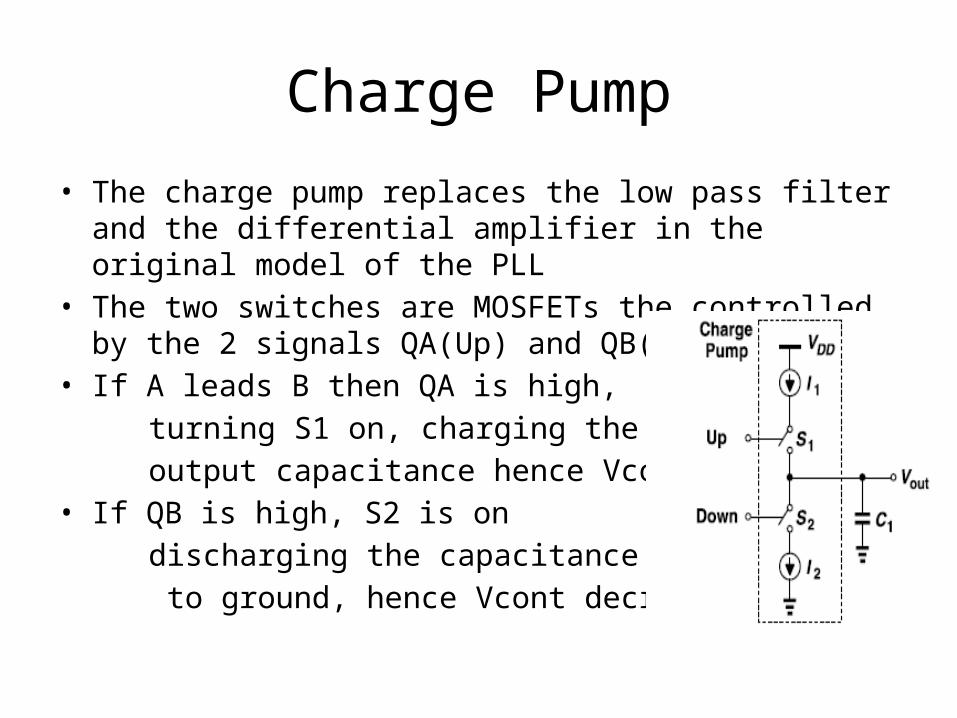
Charge Pump
• The charge pump replaces the low pass filter and the differential amplifier in the original model of the PLL
• The two switches are MOSFETs the controlled by the 2 signals QA(Up) and QB(Down).
• If A leads B then QA is high, turning S1 on, charging the output capacitance hence Vcont increases.• If QB is high, S2 is on discharging the capacitance to ground, hence Vcont decreases.
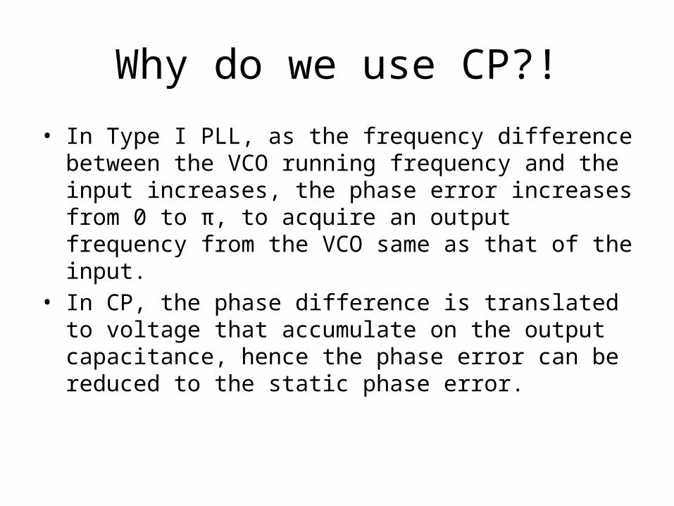
Why do we use CP?!
• In Type I PLL, as the frequency difference between the VCO running frequency and the input increases, the phase error increases from 0 to π, to acquire an output frequency from the VCO same as that of the input.
• In CP, the phase difference is translated to voltage that accumulate on the output capacitance, hence the phase error can be reduced to the static phase error.
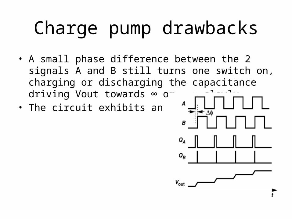
Charge pump drawbacks
• A small phase difference between the 2 signals A and B still turns one switch on, charging or discharging the capacitance driving Vout towards ∞ or - ∞ slowly.
• The circuit exhibits an infinite gain.
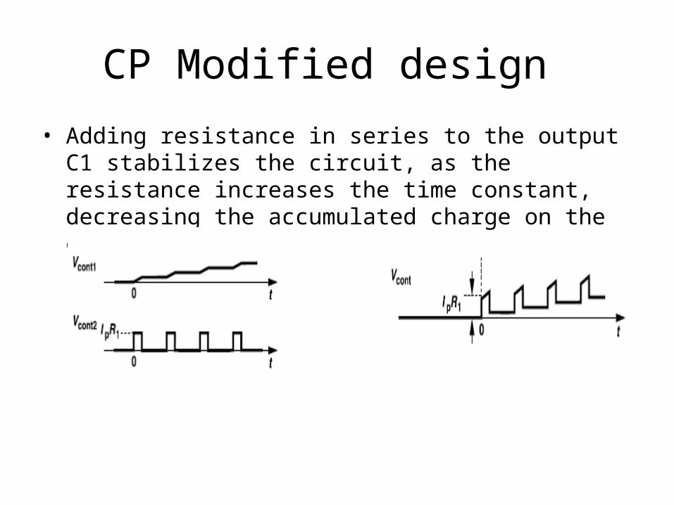
CP Modified design
• Adding resistance in series to the output C1 stabilizes the circuit, as the resistance increases the time constant, decreasing the accumulated charge on the output.
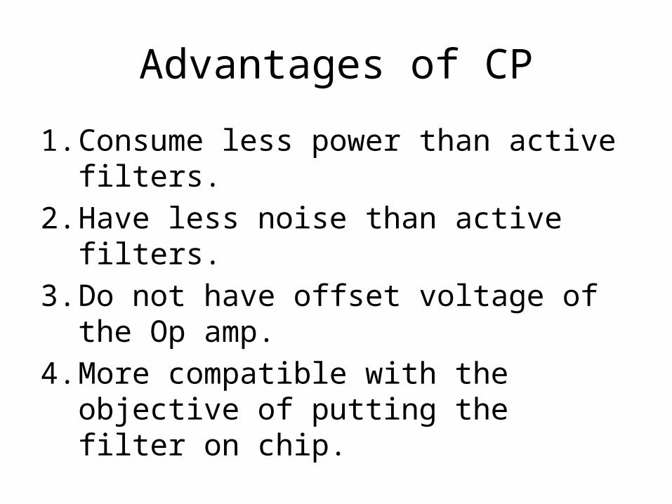
Advantages of CP
1. Consume less power than active filters.2. Have less noise than active filters.3. Do not have offset voltage of the Op amp.4. More compatible with the objective of
putting the filter on chip.
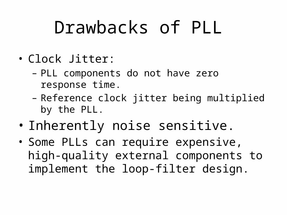
Drawbacks of PLL
• Clock Jitter:– PLL components do not have zero response time.– Reference clock jitter being multiplied by the PLL.
• Inherently noise sensitive.• Some PLLs can require expensive, high-quality
external components to implement the loop-filter design.
PLL Applications
1. FM Demodulator.2. Frequency synthesizer.
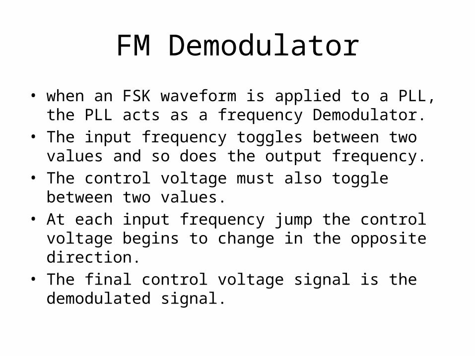
FM Demodulator
• when an FSK waveform is applied to a PLL, the PLL acts as a frequency Demodulator.
• The input frequency toggles between two values and so does the output frequency.
• The control voltage must also toggle between two values.• At each input frequency jump the control voltage begins to
change in the opposite direction.• The final control voltage signal is the demodulated signal.
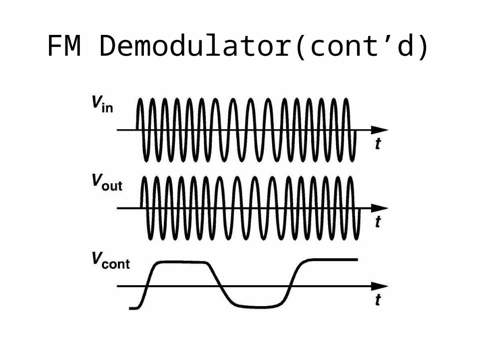
FM Demodulator(cont’d)
FM Demodulator Example:
• For the FM modulator, If and , find for solution
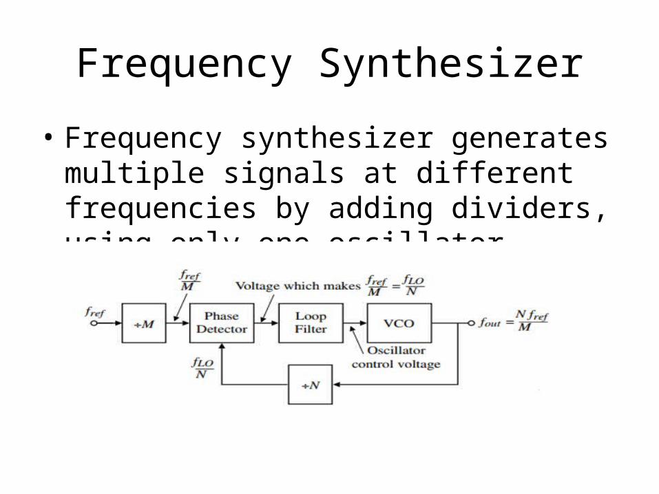
Frequency Synthesizer
• Frequency synthesizer generates multiple signals at different frequencies by adding dividers, using only one oscillator (VCO).
Any Questions ?!
References• RF microelectronics, Behzad Razavi, 2nd version, chapter 9
• PLL Phase Detector / Comparator, http://www.radio-electronics.com/info/rf-technology-design/pll-synthesizers/phase-locked-loop-detector.php
• Introduction to PLL, http://www.digitavid.net/VirtualUniveristy/Presentations/IntroductiontoPLL.pdf
• LECTURE 170 – APPLICATIONS OF PLLS AND FREQUENCY DIVIDERS (PRESCALERS), http://users.ece.gatech.edu/pallen/Academic/ECE_6440/Summer_2003/L170-FreqSyn-I(2UP).pdf
• Introduction to Phase Locked Loops, Kenneth Finnegan, https://www.youtube.com/watch?v=0jzLDe950AY
Thank You ! =)