Embed Size (px)
Citation preview
Phase Change Material Based Ohmic Switches for
Reconfigurable RF Applications
by
Muzhi Wang
A dissertation submitted in partial fulfillment
of the requirements for the degree of
Doctor of Philosophy
(Electrical Engineering)
in the University of Michigan
2017
Doctoral Committee:
Professor Mina Rais-Zadeh, Chair
Professor Katsuo Kurabayashi
Professor Becky Peterson
Professor Kamal Sarabandi

ii
DEDICATION
To my family and friends
iii
ACKNOWLEDGEMENTS
First and foremost, I would like to express my most sincere gratitude to my advisor,
Professor Mina Rais-Zadeh, for the precious opportunity to pursue my Ph.D. degree in
her research group at the University of Michigan, and for her constant guidance and
inspiration throughout the years in my research project. Professor Rais-Zadeh gave me
the chance to work on one of her research projects on my third year as an undergraduate
student. That was the first time that I was introduced to RF MEMS as well as the hands-
on fabrication experience in the cleanroom. This valuable research experience with her
made me decide to continue working on the related field as a graduate Ph.D. student in
her group. In my Ph.D. study, she has inspired a lot of motivation and enthusiasm in our
group, and her guidance and advice has been the key to our research work. My research
project would not have been made possible without her knowledge in RF circuits and
modules, MEMS and integrated Microsystems and phase change materials. I will always
be thankful to her for supporting me and believing in me, and this great Ph.D. study
experience with her will have long-lasting influence in my future career.
I would also like to thank my dissertation committee members for their support on my
research work. Professor Becky Peterson has been both a great professor and a wonderful
friend. She has provided me with great ideas and inspiration that helped me with the
issues and difficulties in my research. Professor Kamal Sarabandi has provided me with
valuable knowledge in RF circuits and systems, and great advice in the direction and big
iv
picture of my research work. Professor Katsuo Kurabayashi’s knowledge mechanical and
thermal related topics and aspects has been a great inspiration to an important part of my
research work.
The Resonant MEMS Group has been a brilliant team of great colleagues and friends
led by Professor Rais-Zadeh. When I first joined the group, it was Dr. Vikram Thakar and
Dr. Yonghyun Shim that mentored me on the research work and the fabrication processes
in the cleanroom. They have provided me with useful knowledge, great techniques and
valuable experience with my research work. Dr. Vikrant Gokhale, Dr. Zhengzheng Wu,
Dr. Azadeh Ansari, Dr. Adam Peczalski, Dr. Roozbeh Tabrizian and Dr. Haoshen Zhu
have also helped me a lot with the theoretical knowledge and in-lab equipment operations.
I am honored to have worked closely with Dr. Feng Lin together on my research related
projects, and grateful for his help with the difficulties I experienced. Mohsen, Cesar and
Milad have also been my great lab mates. I would like to thank all of them for being such
great colleagues and friends.
I would certainly also like to thank all the staff members at the Lurie Nanofabrication
Facility (LNF) at the University of Michigan. None of the research work would have
been possible without their support on the equipment operations and process
development. Their expertise in the fabrication processes and efforts in the tool
maintenance have been the key to my fabrication process. The staff members at the
Michigan Center for Materials Characterization (MC2) have also been very helpful with
the material characterization and electron microscopic imaging processes that I needed to
perform. I am most grateful for their help in the years of my Ph.D. study.
v
I am very grateful to have had the great friends at the University of Michigan and in
Ann Arbor. We share great appreciation for the great college and the wonderful city, and
we value the friendship among one another. Being a graduate student in the College of
Engineering could sometimes be stressful, and the support from my friends has powered
me through times of doubt and depression. I will always cherish the great friendship.
Last but certainly not least, I would like to express my deepest appreciation to my
family, especially my parents, for supporting and encouraging me to pursue my dream,
and for their unconditional love. Finally, I would like to thank my girlfriend Yue for her
love and care. I could not have imagined how wonderful my life would get from the
moment I met her.

vi
TABLE OF CONTENTS
Dedication ....................................................................................................................... ii
Acknowledgements ........................................................................................................ iii
List of Figures .............................................................................................................. viii
List of Tables .............................................................................................................. xviii
List of Abbreviations .................................................................................................... xix
Abstract ....................................................................................................................... xxii
CHAPTER 1 Introduction ................................................................................................... 1
1.1. Motivation and Background ..................................................................................... 1
1.2. Overview of RF Switch Technologies ..................................................................... 3
1.3. Phase Change Materials in Switching Applications .............................................. 11
1.4. Research Objectives and Contributions ................................................................. 13
1.5. Organization of Dissertation .................................................................................. 15
CHAPTER 2 Chalcogenide Phase Change Material ........................................................ 17
2.1. GST Based Phase Change Materials ...................................................................... 18
2.2. Phase Change Material Applications in Non-Volatile Memory ............................ 20
2.3. GeTe Phase Change Material and Switching Activities ........................................ 26
2.3.1. Amorphous versus Crystalline GeTe ............................................................... 26
2.3.2. Phase Transitions between Amorphous and Crystalline States of GeTe ......... 32
2.3.3. GeTe Fabrication Process for RF Switch Applications ................................... 35
2.3.3.1. GeTe Film Deposition Process and Basic Electrical Properties ............... 35
2.3.3.2. GeTe Annealing Process and Crystallization Optimization ..................... 38
2.3.3.3. Atomistic Study of Crystalline GeTe Films.............................................. 40
CHAPTER 3 GeTe Phase Change Material Based RF Ohmic Switches .......................... 44
3.1. Early Designs of Phase Change Material Based RF Switches ............................... 45
3.1.1. RF Switches Using Different Phase Change Materials ................................... 45
3.1.2. Low-Loss Two-Terminal GeTe Based RF Switch .......................................... 47
3.2. Four-Terminal GeTe RF Switches ......................................................................... 51
vii
3.2.1. Four-Terminal GeTe RF Switch with Direct Heating Scheme ....................... 52
3.2.1.1. Device Structure........................................................................................ 53
3.2.1.2. Fabrication Process ................................................................................... 57
3.2.1.3. Measurement Results ................................................................................ 61
3.2.2. Four-Terminal GeTe RF Switch with Indirect Heating Scheme ..................... 73
3.2.2.1. Device Structure........................................................................................ 74
3.2.2.2. Fabrication Process ................................................................................... 77
3.2.2.3. Measurement Results ................................................................................ 86
3.3. Power Handling Analysis and Thermoelectric Modeling ...................................... 93
3.4. Reliability Analysis and Improvement ................................................................... 99
3.4.1. Switch Breakdown Analysis .......................................................................... 100
3.4.2. Switch Reliability Evaluation ........................................................................ 107
3.5. Summary .............................................................................................................. 109
CHAPTER 4 Reconfigurable Bandpass Filter Using GeTe RF Switches ...................... 111
4.1. Motivation and Background ................................................................................. 111
4.2. Design Procedure ................................................................................................. 114
4.3. Fabrication Process .............................................................................................. 120
4.4. Measurement Results ........................................................................................... 122
CHAPTER 5 Conclusions and Future Directions ........................................................... 125
5.1. Thesis Contributions ............................................................................................ 125
5.2. Future Research Directions .................................................................................. 129
5.2.1. GeTe Atomistic Structure Modeling and Analysis........................................ 129
5.2.2. Performance Improvement of GeTe RF Switches ......................................... 130
5.2.2.1. Structural Variations ............................................................................... 131
5.2.2.2. Fabrication Process Improvements ......................................................... 134
Bibliography ................................................................................................................ 137

viii
LIST OF FIGURES
Figure 1.1. The technology trend in semiconductor industry indicating the need for
performance improvement by functional diversification in the “More-than-Moore” era [4].
............................................................................................................................................. 2
Figure 1.2. A FET structure of a microwave switching element proposed in [8]............... 5
Figure 1.3. Simplified cross-sectional view of a GaAs p-i-n diode based on design in [10].
............................................................................................................................................. 6
Figure 1.4. Schematic of a switch using stacking structure to handle higher power [13]. . 8
Figure 1.5. Voltage imbalance caused in switch stacking due to different current flowing
through each transistor [14]. ............................................................................................... 9
Figure 1.6. An RF MEMS switch with a low spring-constant bridge structure [20]. ....... 10
Figure 2.1. Timing diagram of typical temperature profiles for chalcogenide phase
change materials to achieve phase transitions between the crystalline and amorphous
states. ................................................................................................................................. 19
Figure 2.2. Cross-sectional schematic of a typical phase change optical disk with laser
induction as the phase transition method [39] [41] [42]. .................................................. 21
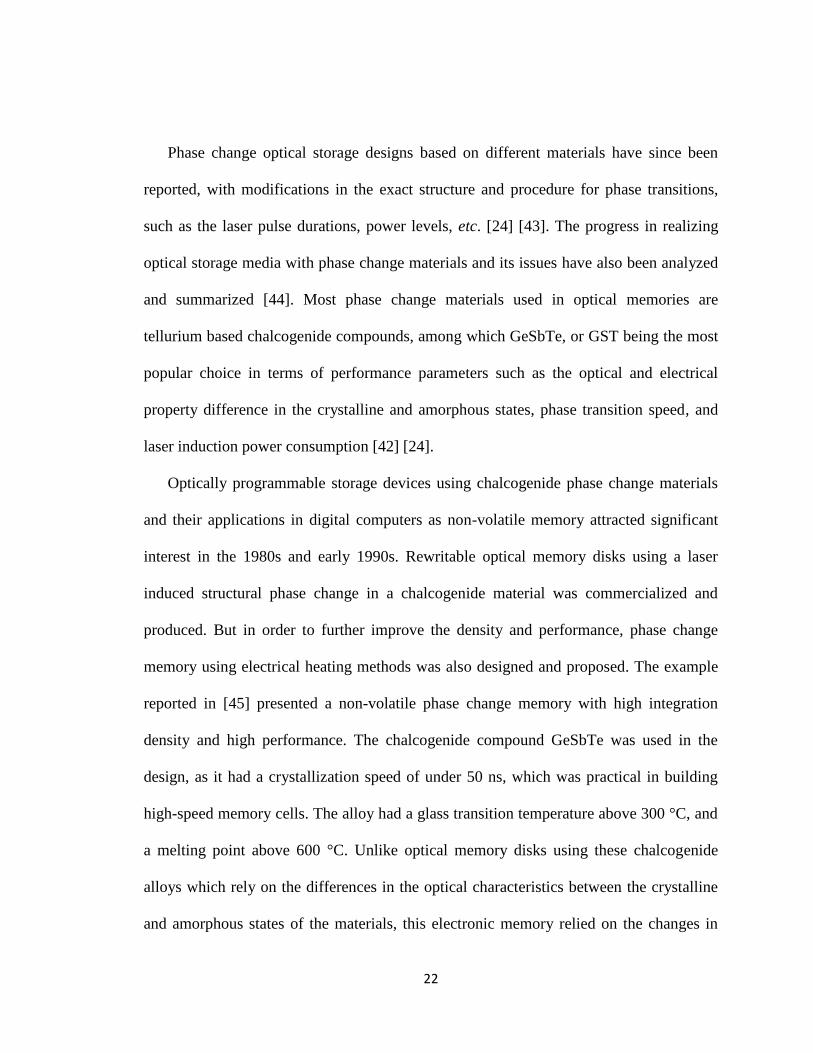
Figure 2.3. Simplified schematic illustration of a memory array circuitry built using
chalcogenide alloy, showing four adjacent memory cells [45]......................................... 23
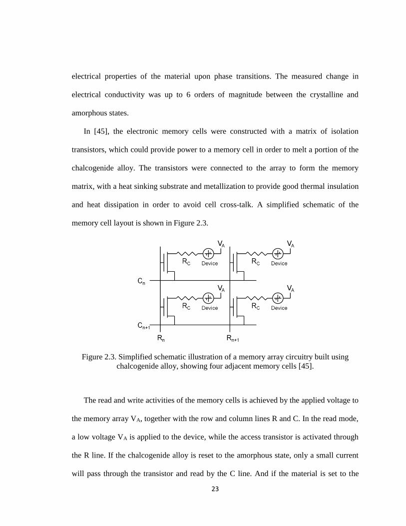
Figure 2.4. Cross-sectional diagram of the phase change via in the memory cell [45]. ... 24
ix
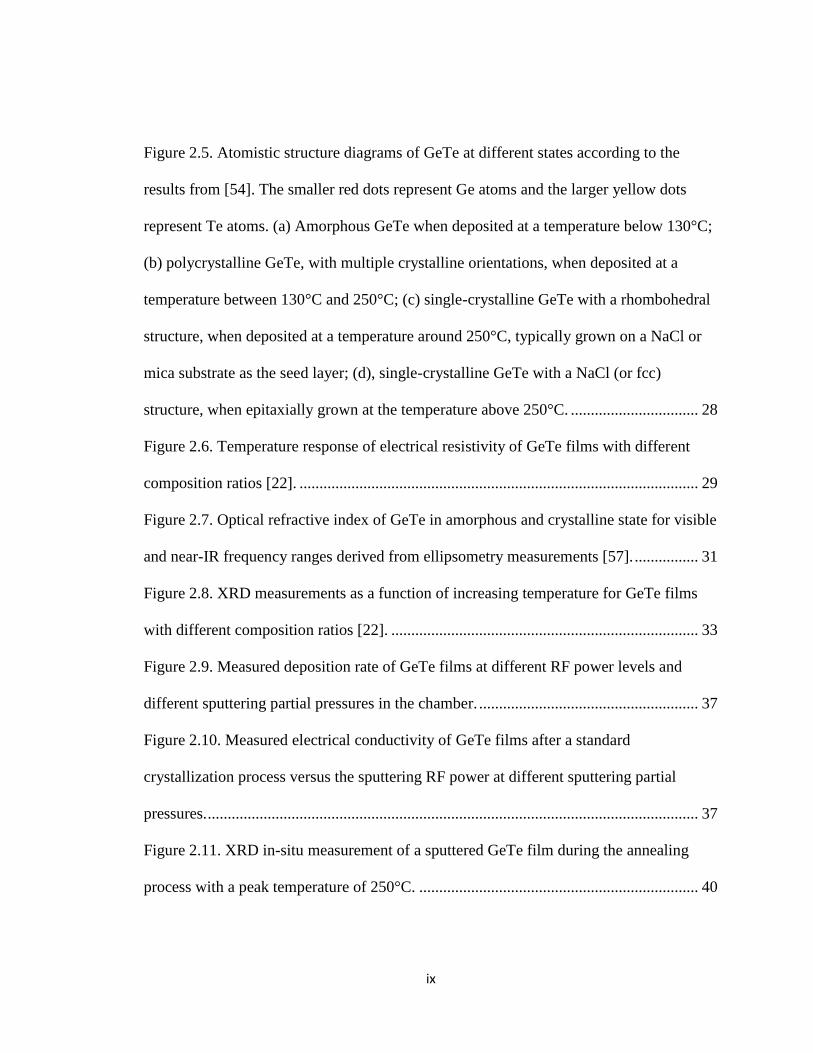
Figure 2.5. Atomistic structure diagrams of GeTe at different states according to the
results from [54]. The smaller red dots represent Ge atoms and the larger yellow dots
represent Te atoms. (a) Amorphous GeTe when deposited at a temperature below 130°C;
(b) polycrystalline GeTe, with multiple crystalline orientations, when deposited at a
temperature between 130°C and 250°C; (c) single-crystalline GeTe with a rhombohedral
structure, when deposited at a temperature around 250°C, typically grown on a NaCl or
mica substrate as the seed layer; (d), single-crystalline GeTe with a NaCl (or fcc)
structure, when epitaxially grown at the temperature above 250°C. ................................ 28
Figure 2.6. Temperature response of electrical resistivity of GeTe films with different
composition ratios [22]. .................................................................................................... 29
Figure 2.7. Optical refractive index of GeTe in amorphous and crystalline state for visible
and near-IR frequency ranges derived from ellipsometry measurements [57]. ................ 31
Figure 2.8. XRD measurements as a function of increasing temperature for GeTe films
with different composition ratios [22]. ............................................................................. 33
Figure 2.9. Measured deposition rate of GeTe films at different RF power levels and
different sputtering partial pressures in the chamber. ....................................................... 37
Figure 2.10. Measured electrical conductivity of GeTe films after a standard
crystallization process versus the sputtering RF power at different sputtering partial
pressures. ........................................................................................................................... 37
Figure 2.11. XRD in-situ measurement of a sputtered GeTe film during the annealing
process with a peak temperature of 250°C. ...................................................................... 40

x
Figure 2.12. XRD in-situ measurement of a sputtered GeTe film during the annealing
process with a peak temperature of 550°C. ...................................................................... 41
Figure 2.13. TEM images of a crystalline GeTe film showing (a) multiple crystalline
orientations within a small imaging area and (b)(c)(d) enlarged view of each area
showing a different crystalline orientation. (e) The diffraction imaging pattern also
suggests a poly-crystalline structure for the GeTe film. ................................................... 43
Figure 2.14. TEM images showing large grain sizes of single crystalline orientations
within the poly-crystalline GeTe film. .............................................................................. 43
Figure 3.1. Cross-sectional schematic of the two-port GeTe-based RF switch [61]. ....... 47
Figure 3.2. SEM images of the GeTe-based RF switches reported in [61] with (a) a single
3m×3m via configuration and (b) a multi-via configuration with five 2m×2m vias
connected in parallel [61]. ................................................................................................. 49
Figure 3.3. Measured resistance of GeTe RF switches with a single-via and multi-via
configurations from DC to 3 GHz when the GeTe via is at the (a) crystalline state and (b)
amorphous state [61]. ........................................................................................................ 49
Figure 3.4. Measured intrinsic capacitance of the GeTe RF switches when the GeTe is at
the amorphous state........................................................................................................... 49
Figure 3.5. Measured and de-embedded S11 and S21 of the GeTe RF switch with the
single-via configuration (a) at the crystalline and (b) amorphous states of GeTe. ........... 50
Figure 3.6. Cross-sectional schematic showing the structure of the four-terminal GeTe RF
switch using the direct heating method. ............................................................................ 53
xi
Figure 3.7. (a) Top-view layout of the heater path in the GeTe switch and its material
combinations. (b) Simplified equivalent circuit model of the heater path. ....................... 54
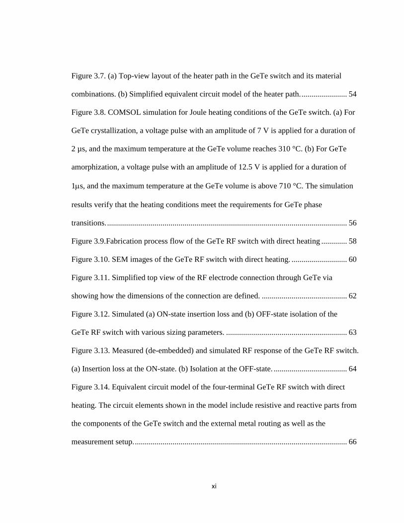
Figure 3.8. COMSOL simulation for Joule heating conditions of the GeTe switch. (a) For
GeTe crystallization, a voltage pulse with an amplitude of 7 V is applied for a duration of
2 µs, and the maximum temperature at the GeTe volume reaches 310 °C. (b) For GeTe
amorphization, a voltage pulse with an amplitude of 12.5 V is applied for a duration of
1s, and the maximum temperature at the GeTe volume is above 710 °C. The simulation
results verify that the heating conditions meet the requirements for GeTe phase
transitions. ......................................................................................................................... 56
Figure 3.9.Fabrication process flow of the GeTe RF switch with direct heating ............. 58
Figure 3.10. SEM images of the GeTe RF switch with direct heating. ............................ 60
Figure 3.11. Simplified top view of the RF electrode connection through GeTe via
showing how the dimensions of the connection are defined. ........................................... 62
Figure 3.12. Simulated (a) ON-state insertion loss and (b) OFF-state isolation of the
GeTe RF switch with various sizing parameters. ............................................................. 63
Figure 3.13. Measured (de-embedded) and simulated RF response of the GeTe RF switch.
(a) Insertion loss at the ON-state. (b) Isolation at the OFF-state. ..................................... 64
Figure 3.14. Equivalent circuit model of the four-terminal GeTe RF switch with direct
heating. The circuit elements shown in the model include resistive and reactive parts from
the components of the GeTe switch and the external metal routing as well as the
measurement setup. ........................................................................................................... 66

xii
Figure 3.15. Demonstration RF power flow within the GeTe switch with direct heating
when it is in the (a) ON-state and (b) OFF-state. In the OFF-state, the high impedance
between the two RF terminals will force a big portion of RF power to flow through the
heater terminals, and thus it is important to ensure good isolation between the heater and
RF terminals. ..................................................................................................................... 69
Figure 3.16. Schematic of the GeTe switch with RF choke modules connected to the
heater terminals during measurement to ensure high isolation between RF and heater
terminals. ........................................................................................................................... 70
Figure 3.17. The S21 response between an RF terminal and a heater terminal from
measurement and simulation with a 100 nH RF choke connected to the heater terminal. 71
Figure 3.18. Simplified block diagram showing the setup for switching speed
measurement for GeTe RF switches. ................................................................................ 72
Figure 3.19. Switching speed measurement of GeTe RF switch with direct heating
scheme (a) from ON to OFF and (b) from OFF to ON. .................................................... 73
Figure 3.20. Cross-sectional schematic showing the structure of the four-terminal GeTe
RF switch using the indirect heating method. ................................................................... 75
Figure 3.21. Thermal simulation using COMSOL FEA software showing the temperature
distribution on the cross-section of the GeTe RF switch with indirect heating when a
heating pulse is applied through the heater layer. ............................................................. 76
Figure 3.22. Fabrication process flow of the GeTe RF switch with direct heating .......... 78
Figure 3.23. Heater embedding process for GeTe RF switches with indirect heating. (a)
Heater embedding without pre-etching of passivation layer, yielding an uneven surface.
xiii
(b) Pre-etching process applied prior to heater layer patterning, resulting in a flat surface.
........................................................................................................................................... 85
Figure 3.24. Heater embedding process with multiple isolation layer deposition and
polishing processes in order to obtain a flat surface before the deposition of GeTe layer.
........................................................................................................................................... 85
Figure 3.25. SEM images of the GeTe RF switch with indirect heating. ......................... 86
Figure 3.26. Measured (de-embedded) and simulated RF response of the GeTe RF switch.
(a) Insertion loss at the ON-state. (b) Isolation at the OFF-state. ..................................... 87
Figure 3.27. Equivalent circuit model of the four-terminal GeTe RF switch with indirect
heating. The circuit elements shown in the model include resistive and reactive parts from
the components of the GeTe switch and the external metal routing as well as the
measurement setup. ........................................................................................................... 88
Figure 3.28. TEM images showing the GeTe RF switch (a) when in the OFF state, (b) the
enhanced view of the GeTe film where only the GeTe volume at the via area is
amorphous, and most GeTe volume remains crystalline. (c) High-resolution TEM image
showing the crystalline-amorphous interface of the GeTe film. ....................................... 90
Figure 3.29. Measured (de-embedded) and simulated RF response of the GeTe RF switch
with modified design showing improved loss performance. (a) Insertion loss at the ON-
state. (b) Isolation at the OFF-state. .................................................................................. 91
Figure 3.30. Switching speed measurement of GeTe RF switch with indirect heating
scheme (a) from ON to OFF and (b) from OFF to ON. .................................................... 92
xiv
Figure 3.31. The thermoelectric model of the GeTe based RF switches. This model
consists of a simplified equivalent circuit model of the phase change switch, and the heat
transfer function as well as the modeling of the changing electrical resistivity of GeTe
with changing temperature and voltage across the phase change layer. ........................... 94
Figure 3.32. Simulated and measured IIP3 of a directly heated switch at (a), (b) crystalline
state and (c), (d) amorphous state with (a), (c) changing center frequency and a constant
50 kHz frequency offset, and (b), (d) changing frequency offset and a constant 2 GHz
center frequency. (a’) – (d’) show the corresponding plots for an indirectly heated switch.
........................................................................................................................................... 98
Figure 3.33. P1dB measurement results for GeTe RF switches (a), (b) with direct heating
scheme and (a’), (b’) indirect scheme and (a), (a’) in ON state and (b), (b’) in OFF state.
The results show that both types of devices have P1dB higher than 20 dBm at both states.
........................................................................................................................................... 99
Figure 3.34. SEM images of a GeTe phase change switch with a breaking point along the
heater path. This breakdown is cause by the high stress generated due to the high voltage
of the heating pulses during phase transitions. ............................................................... 101
Figure 3.35. Thermal simulations using COMSOL on the heater structure with the (a)
SiO2-W-Si3N4 and the (b) AlN-W-AlN material configuration. For both simulations, the
structures and dimensions are kept the same, and the electrical heating pulses are tuned
separately for each simulation to ensure the same temperature profile (with a peak
temperature of approximately 750 °C) is achieved. In the thermal simulations, the thermal
boundaries are defined such that the back side of the Si substrate and the top of the air
xv
box (with a thickness of 100 μm above the device) are at room temperature, and thermal
conduction models are used among the material domains in contact with each other. The
peak stress generated is approximately 228 MPa in (a) and 45.2 MPa in (b)................. 102
Figure 3.36. TEM image of the GeTe layer showing the amorphous-crystalline interface
in the RF switch. In the crystalline GeTe area a lattice orientation can be clearly seen, and
in the amorphous (bright) GeTe area the lattice can hardly be seen. .............................. 103
Figure 3.37. TEM image of amorphous GeTe with material fatigue failing further phase
transitions. In the image, small scattered crystalline areas can be seen, but the GeTe is
mostly amorphous. .......................................................................................................... 104
Figure 3.38. Energy-dispersive X-ray spectroscopy (EDXS) measurements of the GeTe
film in the RF switch (a) before any switching activities have been applied and (b) after
the device has failed switching after a certain amount of switching activity. ................ 106
Figure 3.39. Resistance response of the indirectly heated switch measured with repeated
switching activities using thermal actuations. ................................................................ 107
Figure 3.40. : ON and OFF state resistance of GeTe switches using indirect heating, after
each time a successful phase transition through a heating pulse is observed. (a) a
resistance value above 10 kΩ is treated as a successful transition to the OFF state, and the
resistance values at both states are generally stable with occasional fluctuations; (b) a
resistance value above 1 kΩ is treated as a successful transition to the OFF state, and the
ON state resistance values are more stable in comparison to (a). ................................... 108
Figure 4.1. The schematics of the X-band reconfigurable bandpass filter using GeTe
based RF switches showing (a) the entire circuit model, (b) the section with the coupled

xvi
resonators, and (c) the circuit model of the resonator with the external coupling circuit.
......................................................................................................................................... 116
Figure 4.2. Desired and achieved coupling coefficients of the coupled resonators in the
filter as a function of frequency. ..................................................................................... 117
Figure 4.3. Simulated S-parameters of the GeTe RF switch showing the insertion loss and
isolation used as a reference for the simulation of the filter design................................ 119
Figure 4.4. Top-view layout of the reconfigurable bandpass filter using GeTe based RF
switches. A zoomed-in view of a GeTe RF phase change switch is also included. ....... 119
Figure 4.5. Cross-sectional schematic showing structure of the filter design. The
microstrip lines share the gold layer from the GeTe switches. This diagram is intended to
show the layer configuration, and does not reflect the actual device layout. The device
layout is shown in Figure 4.4. ......................................................................................... 120
Figure 4.6. Fabrication process flow of reconfigurable bandpass filters using GeTe phase
change switches. ............................................................................................................. 121
Figure 4.7. Microscope image of the fabricated reconfigurable bandpass filter. ........... 122
Figure 4.8. Measured and simulated S-parameters of the reconfigurable bandpass filter
using GeTe switches. ...................................................................................................... 123
Figure 4.9. Measured IIP3 at the (a) downlink band (7.45 GHz) (b) uplink band (8.07
GHz) of the reconfigurable bandpass filter. .................................................................... 123
Figure 4.10. Measured S21 of the filter at varying input power levels at the (a) downlink
band (7.45 GHz) (b) uplink band (8.07 GHz). ................................................................ 123
xvii
Figure 5.1. An alternative structure of the four-terminal GeTe based RF ohmic switch
using direct heating with two heater terminals laterally connected and two RF terminals
vertically connected by the GeTe via.............................................................................. 131
Figure 5.2. An alternative structure of the four-terminal GeTe based RF ohmic switch
using indirect heating with a top heater configuration. ................................................... 132
Figure 5.3. An alternative structure of the four-terminal GeTe based RF ohmic switch
using indirect heating with an embedded heater and a vertically connected RF signal path.
......................................................................................................................................... 133
xviii
LIST OF TABLES
Table 2.1. Electrical conductivity measurements of GeTe films crystallized at different
peak oven temperatures..................................................................................................... 39
Table 3.1. Material properties of dielectric layers and parameters used in thermal analysis
........................................................................................................................................... 81
Table 3.2. Comparison of performance among different GeTe RF switch designs ......... 93
Table 3.3. Comparison of RF switch designs using different technologies.................... 110
Table 4.1. Constant parameters used in the design calculations. .................................... 117
Table 4.2. Performance comparison of the GeTe RF switch based reconfigurable
bandpass filter to other reported designs targeting the similar frequency range. ........... 124
xix
LIST OF ABBREVIATIONS
AC Alternating current
ACP Air coplanar
AlN Aluminum nitride
BW Bandwidth
CABW Constant absolute bandwidth
CMOS Complementary metal-oxide-semiconductor
CMP Chemical mechanical planarization
DC Direct current
DRAM Dynamic random access memory
EDXS Energy-dispersive X-ray spectrometry
fcc Face-centered cubic
FEA Finite element analysis
FET Field-effect transistor
FIB Focused ion beam
GaAs Gallium arsenide
GeSb Germanium antimonide
GeTe Germanium Telluride
GGG Gadolinium gallium garnet
GSG Ground-signal-ground
xx
GST/GeSbTe Germanium antimony telluride
IIP3 Input third-order intercept point
IoT Internet of Thing
ITRS International Technology Roadmap for Semiconductors
LNF Lurie Nanofabrication Facility
MEMS Micro-electromechanical system
MOSFET Metal-oxide-semiconductor field-effect transistor
NaCl Sodium chloride
OIP3 Output third-order intercept point
P1dB 1-dB compression point
PECVD Plasma-enhanced chemical vapor deposition
HEMT High electron mobility transistor
RAM Random access memory
RF Radio frequency
SEM Scanning electron microscopy
Si3N4 Silicon nitride
SiO2 Silicon dioxide
SOI Silicon-on-insulator
SOS Silicon-on-Sapphire
SP6T Single-pole-6-throw
SPDT Single-pole-dual-throw
SPMT Single-pole-multiple-throw

xxi
SPST Single-pole-single-throw
TCR Temperature coefficient of resistance
TEM Transmission electron microscopy
TiN Titanium nitride
TiW Titanium-tungsten
Tx/Rx Transmitter/receiver
XRD X-ray diffraction
YIG Yttrium iron garnet
xxii
ABSTRACT
This research work is focused on the study and development of chalcogenide phase
change materials and their applications in reconfigurable RF modules and systems.
Germanium telluride (GeTe), one of the chalcogenide phase change materials, is studied
and used in the development process of RF ohmic switches. This thesis presents the study
of GeTe and other phase change materials, the design, fabrication and measurements of
GeTe phase change material based RF switches, and the performance evaluation as well
as the operation and breakdown analysis of the GeTe phase change RF switches. It also
discusses the potential applications of GeTe RF switches in reconfigurable RF modules
by demonstrating a bandpass filter design.
RF switches based on solid-state transistors and diodes, and micro-electromechanical
system (MEMS) as well as other technologies have been reported and used in integrated
circuits and systems for RF and microwave applications. Each of these technologies for
RF switches shows some limitations regarding RF performance, integration compatibility,
cost, fabrication yield, or reliability. This thesis presents a novel alternative for RF switch
development using GeTe phase change material. The special phase transition properties
of phase change materials have drawn attention for decades. Material study and
characterization of phase change materials have been performed for a better
understanding of their properties. Phase change materials have since been developed for
different applications, with non-volatile memory modules being the most successful
xxiii
application. With the success in phase change memory design, we have directed our
attention to RF switching applications based on phase change materials. Two main types
of GeTe phase change material based RF ohmic switches are developed and the design
and fabrication of each is discussed in detail. The RF switches designed using GeTe have
shown very competitive performance results compared to other existing RF switch
designs. Analysis and modeling of the switches have also been performed for a better
understanding of the devices and phase change materials as well as their phase transition
process. A reconfigurable bandpass filter using GeTe switches have verified the good
functionality of phase change RF switches and their promising potential in reconfigurable
RF applications.
1
CHAPTER 1 Introduction
1.1. Motivation and Background
Radio Frequency (RF) modules are widely used in wireless communication systems
such as radars and wireless transceivers. In modern designs, RF systems are commonly
realized with on-chip integrated circuits. In mobile wireless communication systems, for
example, they usually serve as the signal transmitting and receiving front-ends for the
baseband analog and digital processing systems. Due to the coexistence of different
wireless communication standards in the radios, band switching among different
frequencies is often required, which is realized through module or system level
reconfigurability. In reconfigurable systems, the key element is the RF switch. Some of
the requirements for RF switches include low transmission or insertion loss, high
isolation between the input and output RF terminals in the OFF mode, fast switching
speed, high RF power handling capability, and high operation linearity across a certain
RF power level.
In modern wireless communication systems, RF switches are commonly used for
purposes such as Tx/Rx selection, frequency band selection, signal relay and other
network reconfiguration activities. Along other tuning/reconfiguring techniques, RF
switches are critical in achieving system level reconfigurability in emerging technologies
such as the internet of things (IoT). A vast number of solid-state based RF switches have
been designed and used in RF systems since several decades ago using various
2
semiconductor techniques such as silicon on insulator (SOI) or gallium arsenide (GaAs)
based integrated circuitry [1, 2, 3]. As predicted by Moore’s Law, the number of
transistors on a densely integrated circuit doubles in approximately every two years, and
the semiconductor industry has been able to follow Moore’s Law over the past several
decades. In the progression of transistor integration density, miniaturization has played a
critical role, with the size of transistors reduced as fabrication technology improved. In
recent years, however, as transistor sizes get closer to their physical limits, Moore’s Law
regarding transistor density is becoming harder to follow. In order to sustain the
performance improvement of integrated circuits, utilization of new materials and novel
device structures is becoming more critical. This trend in semiconductor technology
development is known as the “More-than-Moore” era according to the International
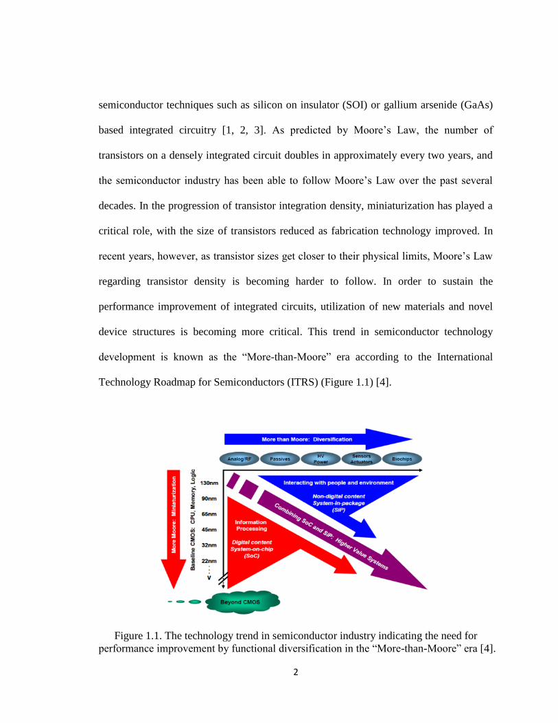
Technology Roadmap for Semiconductors (ITRS) (Figure 1.1) [4].
Figure 1.1. The technology trend in semiconductor industry indicating the need for
performance improvement by functional diversification in the “More-than-Moore” era [4].
3
1.2. Overview of RF Switch Technologies
RF and microwave switches have been designed and used in semiconductor
integrated circuits and microsystems for control and signal relay purposes. They are
among the most effective ways to achieve system configurability. One example of RF
switch applications is the RF front-end for wireless communications. In a typical front-
end module, single-pole double-throw (SPDT) antenna switches are usually used for
selection between the transmitter and receiver modules. For a multi-band front-end
module, single-pole multiple-throw (SPMT) RF switches are used for band selection. As
wireless products, such as radio transceivers, hand-held devices and other portable
devices, become popular in industry and consumer market, the need for improving
performance and reducing costs of RF transceivers becomes more noticeable [5]. As RF
switches are an important part of wireless RF modules, their performance and cost
requirements are also becoming stringent. One of the most important performance
requirements for RF switches is the signal transmission and isolation values. High-
performance RF switches need to have low signal insertion loss when turned ON, and
high signal isolation when turned OFF. Other performance requirements that are common
among RF modules include switching speed, indicating how fast the switch can be turned
ON or OFF, linearity, indicating whether the switch can operate with minimal harmonics
and intermodulation products at frequencies, power consumption, and power handling
capability, showing what RF power level the switch can handle without showing
degraded functionality. Other than the common performance requirements for RF
switches, there are also requirements for good integration compatibility, reasonable
4
device size, and ease of fabrication technology. RF switches are also preferred to have a
low-cost fabrication process with a high yield, in order to reduce the overall cost. Taking
all the requirements and specifications into account, a number of RF switch designs have
been proposed, built, and used in RF systems.
In semiconductor integrated systems, field effect transistor (FET) based switches are
among the earliest switch designs that were developed. Considering the physical
properties of FETs, they can be readily implemented as gate-controlled switching devices.
Their fabrication process also makes them compatible for co-integration with other
semiconductor based modules and systems [6]. Different types of FETs and their
microwave operation have been comprehensively summarized in [6], and a dual-gate
metal-oxide-semiconductor FET (MOSFET) based amplifier design has been reported,
demonstrating a 60-dB dynamic switching range and high switching speed at 4 8 GHz
[7]. Significant progress has been made in the development of FETs for microwave
applications since 1970’s, and various FET based switch designs have been proposed.
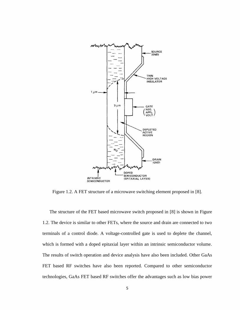
One of the proposed designs is an FET microwave switch based on gallium arsenide
(GaAs) [8].
5
Figure 1.2. A FET structure of a microwave switching element proposed in [8].
The structure of the FET based microwave switch proposed in [8] is shown in Figure
1.2. The device is similar to other FETs, where the source and drain are connected to two
terminals of a control diode. A voltage-controlled gate is used to deplete the channel,
which is formed with a doped epitaxial layer within an intrinsic semiconductor volume.
The results of switch operation and device analysis have also been included. Other GaAs
FET based RF switches have also been reported. Compared to other semiconductor
technologies, GaAs FET based RF switches offer the advantages such as low bias power
6
in both states and low loss [2]. The GaAs FET based RF switches reported in [1] also
show good power handling capability. An integrated SPDT switch based on GaAs FET
has also been reported for mobile communication systems, showing a high-power
handling capability of over 5 W (37 dBm) [9]. GaAs FET-based switches have been
popular in RF and microwave applications, but they also show certain limitations, such as
high level of distortion, especially in the OFF state, caused by the junction capacitance
non-linearity [2].
Other than FET-based RF switches, GaAs p-i-n diode based switches have also been
designed. RF and microwave switches built with p-i-n diodes are also very popular due to
their high breakdown voltages, fast switching characteristics, variable resistance with bias
and broadband application capability [3].
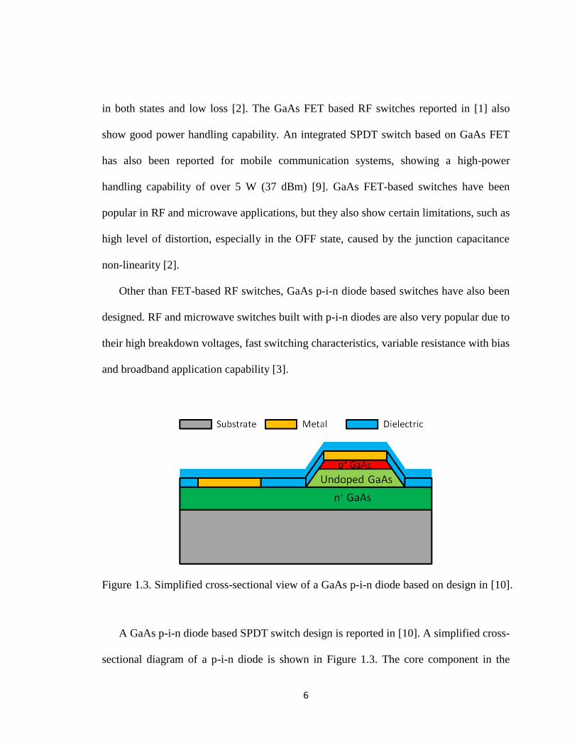
Figure 1.3. Simplified cross-sectional view of a GaAs p-i-n diode based on design in [10].
A GaAs p-i-n diode based SPDT switch design is reported in [10]. A simplified cross-
sectional diagram of a p-i-n diode is shown in Figure 1.3. The core component in the

7
device is the p-type and n-type doped GaAs regions, separated by an undoped GaAs
region. Based on p-i-n junction physics, the conductivity between the p and n terminals of
the switch is controlled by the DC bias voltage, and this is how the switching activities
are controlled. The design in [10] has shown an insertion loss of approximately 1 dB and
an isolation above 35 dB up to 30 GHz, which indicates high performance and broadband
capability.
The silicon-on-sapphire (SOS) technology, which utilizes a structure of a thin silicon
layer on top of a sapphire layer on a silicon substrate, has provided higher performance in
RF and microwave applications. Compared to traditional silicon processes, the SOS
process is able to eliminate the parasitic capacitances generated from the bulk substrate,
and therefore is preferred for high frequency operations. An example of a SOS CMOS
RF switch design is proposed in [11]. The reported switch with an SP6T structure was
able to provide an insertion loss of less than 1 dB, and an isolation above 40 dB up to 2.5
GHz, and a high power handling with a 1-dB compression (P1dB) of 20 W (43 dBm), and
an output third-order intercept point (OIP3) above 70 dBm, which indicates good RF
performance, linearity, and power handling capability.
Silicon-on-insulator (SOI) is another commonly used technology for RF integrated
circuits. SOI based RF switches are designed and used in RF transceivers and other
applications. SOI structure uses a stack with a thin silicon layer on top of a buried oxide
layer on the handling wafer. Like SOS, this insulating structure is also used to reduce the
issue with substrate parasitic coupling [12]. While GaAs and SOS technologies tend to
8
suffer from cost and integration disadvantages, SOI offers a lower cost and easier
integration process into silicon based systems, while maintaining good performance.
One issue that is common to Si, SOI, and SOS FET-based devices is the relatively
low breakdown voltage. In order for the switches to handle higher voltages without
breaking down, the method of switch stacking is very commonly used. This method
involves stacking multiple FET switches in series, and through the voltage distribution
across the switches, a higher voltage or power can be handled [11, 13].
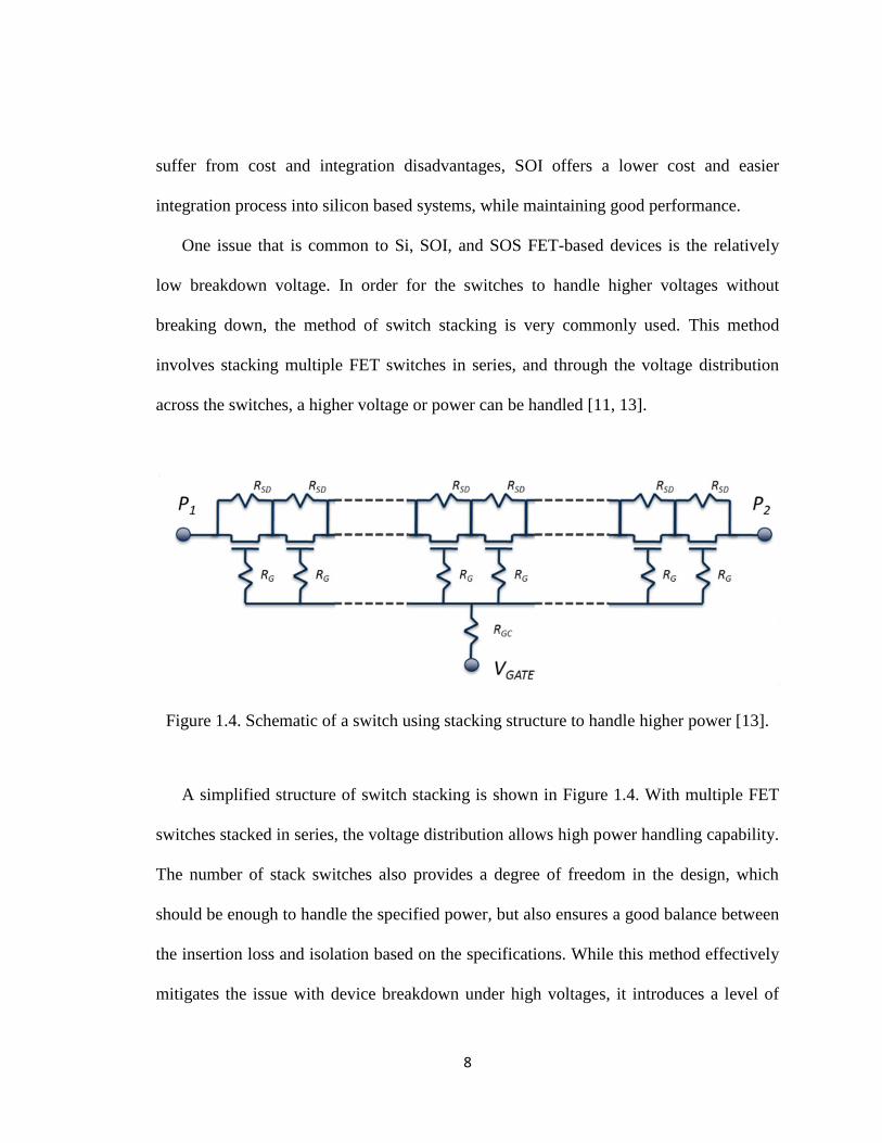
Figure 1.4. Schematic of a switch using stacking structure to handle higher power [13].
A simplified structure of switch stacking is shown in Figure 1.4. With multiple FET
switches stacked in series, the voltage distribution allows high power handling capability.
The number of stack switches also provides a degree of freedom in the design, which
should be enough to handle the specified power, but also ensures a good balance between
the insertion loss and isolation based on the specifications. While this method effectively
mitigates the issue with device breakdown under high voltages, it introduces a level of
9
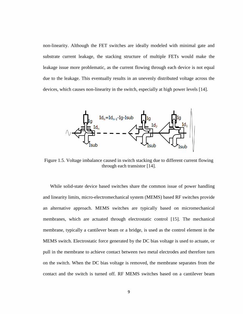
non-linearity. Although the FET switches are ideally modeled with minimal gate and
substrate current leakage, the stacking structure of multiple FETs would make the
leakage issue more problematic, as the current flowing through each device is not equal
due to the leakage. This eventually results in an unevenly distributed voltage across the
devices, which causes non-linearity in the switch, especially at high power levels [14].
Figure 1.5. Voltage imbalance caused in switch stacking due to different current flowing
through each transistor [14].
While solid-state device based switches share the common issue of power handling
and linearity limits, micro-electromechanical system (MEMS) based RF switches provide
an alternative approach. MEMS switches are typically based on micromechanical
membranes, which are actuated through electrostatic control [15]. The mechanical
membrane, typically a cantilever beam or a bridge, is used as the control element in the
MEMS switch. Electrostatic force generated by the DC bias voltage is used to actuate, or
pull in the membrane to achieve contact between two metal electrodes and therefore turn
on the switch. When the DC bias voltage is removed, the membrane separates from the
contact and the switch is turned off. RF MEMS switches based on a cantilever beam

10
structure have been reported with successful switching activities and good RF
performance [16, 17]. In order to reduce the DC bias voltage required for switch
actuation, alternative structures have been proposed. A bridge structure design with
meandering supports of the membrane has shown a DC bias voltage as low as 9 V to
successfully actuate the MEMS switch [18]. Other than ohmic RF MEMS switches,
where the metal electrodes come in direct contact when the switch is turned on, a
capacitive RF MEMS switch has a structure where the membrane forms a capacitor with
the bottom metal, and is functional at high frequencies [19].
Figure 1.6. An RF MEMS switch with a low spring-constant bridge structure [20].

11
A top view of an RF MEMS switch is shown in Figure 1.6 [20]. The top membrane in
the switch is built into a bridge structure that is anchored at the four corners. The
membrane is connected to the anchors through four folded beam in order to reduce the
spring constant, which reduces the pull-in voltage required. The membrane has a top and
bottom pull-in electrodes, and a center capacitive area that comes in contact with the
bottom structure when an actuation voltage is applied. Since RF MEMS ohmic switches
use mechanical structures where metal electrodes come in contact to achieve switching,
they tend to provide very low insertion loss and high isolation compared to solid-state
transistor or diode based switches. However, due to the mechanical structures and mobile
components, the fabrication process is usually complicated and has relatively low yield,
and the size of MEMS devices are usually much larger compared to transistors or diodes.
Therefore MEMS-based RF switches have the limitations of high cost and non-ideal
integration compatibility.
1.3. Phase Change Materials in Switching Applications
A new approach of RF ohmic switch implementation has been introduced with the
study of phase change materials. Phase change, or resistance change materials, refer to a
class of chalcogenide compounds that possess two phases at room temperature: a
crystalline phase and an amorphous phase, which can be thermally driven from one state
to the other [21]. One of the most significant differences between the crystalline and
amorphous states is the drastically different electrical resistivity, which can be several
orders of magnitude [22]. The phase transition property and the difference in electrical
12
resistivity makes phase change material an excellent switching element that can
potentially be used in RF and microwave applications.
Phase change materials were first discovered and identified as a type of disordered
semiconductors that can experience rapid and reversible transitions between a highly
resistive state and highly conductive state [23]. Phase change materials that have been
discovered include chalcogenide compounds consisting of a combination of tellurium
(Te), germanium (Ge) and/or antimony (Sb) with doping elements such as indium (In),
oxygen (O), selenium (Se), tin (Sn), etc. Although they do not behave the same under
certain thermal and electrical conditions, they share the same property of phase
transitions. Because of this property, phase change materials have been used to develop
non-volatile memory modules for the past few decades in response to the scalability
challenges of non-volatile memory based on floating gate and other technologies [24, 25].
Phase change materials can be scaled down to very small resistive vias, which satisfies
the size requirements for memory cells. Their resistivity ratio between the amorphous and
crystalline states makes it easy to store information, which ensures good functionality of
the memory designs. More details about phase change materials and their applications in
non-volatile memory are discussed in the following chapter.
With the same properties that are being used in memory applications, phase change
materials are also showing great potential in switching modules for RF and microwave
applications. Their low electrical resistivity in the crystalline state ensures low resistance
when connecting RF terminals, which is the key to low insertion loss for switch designs.
The high electrical resistivity in the amorphous state, on the other hand, ensures high
13
isolation between RF signal transmission terminals. Compared to solid-state based
switches, phase change material based switches offer higher performance, and with the
simple resistive via structure, they offer higher integration density than transistor based
switches. Compared to MEMS based RF switches, they have the advantages of small size
and simple structure, which essentially means easier fabrication process, lower cost, and
better integration compatibility. Because of the great potential of phase change materials
and their successful insertion non-volatile memory applications, phase change material
based RF switches offer a novel and promising solution to switching applications for
integrated circuits and systems for the “More-than-Moore” era.
1.4. Research Objectives and Contributions
The main objective of this work is to develop GeTe-based ohmic switches for RF
applications with RF performance that is comparable to or better than existing solid-state
and MEMS-based RF switches. The performance requirements include good insertion
loss and isolation value in the target frequency range, good power handling capability and
high linearity performance, as well as reliable switching performance.
This research work to develop a GeTe phase change material based ohmic switch for
RF applications has achieved the following milestones:
Design and fabrication of four-terminal GeTe-based phase change RF switches
using direct heating or indirect heating methods: Both types of switches have been
measured to have an insertion loss below 0.5 dB and isolation above 13 dB
through the frequency range from DC to 20 GHz. The figure-of-merit cut-off
14
frequency (𝑓𝑐𝑜, defined as 1/(2 ⋅ 𝜋 ⋅ 𝑅𝑜𝑛 ⋅ 𝐶𝑜𝑓𝑓)) is above 4 THz. The switches
have shown reliable switching activities of up to hundreds of cycles. The four-
terminal switch design using direct heating method was the first to be
demonstrated in the literature and has been patented.
Development of a thermoelectric model to analyze the electrical and thermal
response of the switches at varying RF power levels and with different heating
power levels: This modeling method is used to explore the linearity performance
and power handling capability of the switch. Corresponding 1-dB compression
point (P1dB) and input third-order intercept point (IIP3) measurements are taken to
verify this model.
Design and fabrication of a reconfigurable bandpass filter for X-band applications
using the GeTe phase change material based RF switches: This design uses the
GeTe switches as a proof of concept to show their application in reconfigurable
RF modules. The bandpass filter has two operating bands, both of which show an
insertion loss of less than 3.2 dB, a bandwidth around 500 MHz and an estimated
quality factor of 59.
Material study of GeTe with the assistance of scanning electron microscopy
(SEM), transmission electron microscopy (TEM) and other optical measurements
and imaging methods to better understand the phase transition process of GeTe on
the atomic level as well as the cause of phase transition failures.
15
1.5. Organization of Dissertation
This dissertation is divided into five chapters to discuss the related research work in
different perspectives. Chapter 1 of the dissertation provided an introduction of Ohmic
switch applications in RF modules, and the motivation behind the development of novel
RF switches using phase change materials. Chapter 2 discusses the properties of phase
change materials. It summarizes the discovery and development process of chalcogenide
phase change materials of different types, and their applications in non-volatile memory
modules. It then specifically discusses GeTe properties reported in literature as well as
those characterized during the course of this Ph.D. research. It also provides detailed
observation of GeTe phase transition behavior and its corresponding electrical and optical
property change. Chapter 3 discusses detail design and development procedure of RF
ohmic switches based on GeTe. In Chapter 3, different types of GeTe-based RF ohmic
switches are shown and their structure, principle of operation, design procedure,
fabrication process and performance evaluation are detailed. Chapter 3 also provides the
thermoelectric modeling method for the GeTe RF switches that relates the thermal
properties of the switches to their electrical properties. Testing and characterization
results of the switch reliability study are also shown in Chapter 3. Chapter 4 of this
dissertation presents a reconfigurable bandpass filter using GeTe RF switches for X-band
wireless applications. In Chapter 4, the design process, device structure, fabrication
process, and the measurement results of the phase change filter are provided to prove the
applicability of phase change switches in reconfigurable RF modules. Finally, Chapter 5
16
of this dissertation summarizes the achievements and contributions of this research work,
and it also provides possible future research directions for continuation of this research.
17
CHAPTER 2 Chalcogenide Phase Change Material
Over the past few decades, chalcogenide compounds, or chalcogenide materials have
received increased attention for consumer electronics applications. A series of shared
special properties among various chalcogenide compounds have been observed.
Chalcogenide compounds are most recognized by their interchangeable states at room
temperature. Typically, a chalcogenide material possesses two or more states at which it
exhibits different material properties. Some of the most studied properties of
chalcogenide compounds include material crystallinity, electrical resistivity, dielectric
relative permittivity, and optical index of refraction. One of the earliest reports on such
material behaviors is by Ovshinsky [23], in which various materials called disordered
semiconducting materials were observed to experience rapid and reversible transitions
between a highly resistive and a highly conductive state effected by an electrical field.
One reported experiment in [23] used a sputtered film of an amorphous semiconductor
containing 48 at.% tellurium (Te), 30 at.% arsenic (As), 12 at.% silicon (Si) and 10 at.%
germanium (Ge). The specimen was structured with two carbon electrodes where voltage
signals of different frequencies were applied. The measurements showed repeatable
switching activities between a highly resistive state and a highly conductive state,
achieved by crossing above or below a holding voltage, Vh, across the electrodes.
Since [23], more efforts have been made to achieve phase transitions of chalcogenide
materials through different measures and to systematically categorize and analyze the
18
phase transition activities of these materials. Reported methods to achieve repeatable
phase transitions within chalcogenide materials, other than application of electrical field
mentioned in [23], include laser (light) excitation [26], surface-nucleation through
melting and quenching [27], etc. In the early reported works, the materials used in the
experiments consisted of an element combination of arsenic (As), germanium (Ge),
tellurium (Te), antimony (Sb) and/or sulfur (S).
More phase transition experiments and analysis on chalcogenide materials have since
been reported [28] [29] [30] [31]. The most commonly recognized chalcogenide materials
with the phase transition property include semiconductor compounds with Ge, Sb and Te,
with various combinations and stoichiometric percentages. Due to the state transitions
between a highly conductive state and a highly resistive state, this type of chalcogenide
materials is also known as phase change, or resistance change materials.
2.1. GST Based Phase Change Materials
GST, or GeSbTe, refers to the type of phase change materials with the combination of
Ge, Sb and Te. Common examples of this family of phase change materials include
germanium telluride (GexTey, or GeTe), germanium antimony telluride (GexSbyTez, or
GeSbTe) and germanium antimonide (GexSby, or GeSb). Most GST-based materials
possess two states at room temperature, known as the crystalline state and the amorphous
state, distinguished by their very different material crystallinity [22]. In the crystalline
state, they tend to exhibit very low, metal-like electrical resistivity, while in the
amorphous state, they usually behave like dielectric materials with very high electrical
19
resistivity and varying dielectric constants [32]. Other differences such as optical
properties can also be observed. These differences between the two states are due to the
different atomic structures [33]. Phase transitions between the two states within these
materials are essentially achieved by thermal actuation, with the material heated up to a
certain temperature, followed by a cooling process with a certain cooling speed [21].
Typically, the phase transition process from the crystalline state to the amorphous state
(also known as amorphization process) involves a heating process with a high peak
temperature, in some cases above the material’s melting point, and a cooling process that
is relatively fast. The phase transition process from the amorphous state to the crystalline
state (also known as crystallization process) has a relatively lower peak temperature,
normally within what is known as the crystallization temperature zone, and a lower
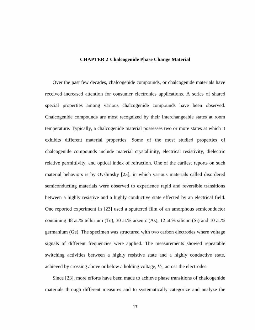
cooling speed in comparison, to allow the process of crystallization [34]. A graphic
illustration and comparison of the temperature profiles for phase transitions in both
directions is shown in Figure 2.1.
Figure 2.1. Timing diagram of typical temperature profiles for chalcogenide phase
change materials to achieve phase transitions between the crystalline and amorphous
states.
Te
mp
era
ture
t
Crystallization
Temp. zone
Melting temperature
Temp. with OFF Pulse
Temp. with ON PulseOFF Pulse
ON Pulse
Glass Temp. zone
20
Due to the large electrical resistance ratio [22] [32] and fast phase transition time [34],
phase change materials have been used for various applications where fast changes of
electrical resistances can be conveniently utilized. The earliest and most common
applications of phase change materials include non-volatile memory [35] and switching
devices [36], which are detailed below.
2.2. Phase Change Material Applications in Non-Volatile Memory
Optical storage applications based on the reversible phase transformation between the
crystalline and amorphous states of chalcogenide materials were first studied in the early
1970s [26]. Earliest efforts on realizing phase change reversible storage have been made
using materials such as TeGeSnOx [37], TeGeSnAu [38], InSe [39], GeTe [35] and
GeSeTe [40]. In order to achieve reversible phase transitions from/to the crystalline state
to/from the amorphous state, most commonly reported methods include laser induction,
with a more rapid crystallization/amorphization process, and heating state induction,
which can be realized by either the application of electrical pulses or in some cases
programmed ovenization.
At the early development stages of phase change memories, laser induction was very
commonly used as the phase transition method [38] [39] [41] due to the ease of the power
delivery process and effectiveness in phase transitions. The typical power level of the
applied laser pulses has been within 100 mW, with a pulse duration of less than 500 ns
[39] [41], depending on the structure of the memory cell, the phase change material used
as the recording film, and whether the phase transition is crystallization or amorphization.

21
Normally a dual beam configuration is required in the structure, since the crystallization
time of the phase change material is usually less than 100 ns, typically around 50 ns, and
the amorphization time is between 200 ns and 500 ns; the time difference is too large for
the same pulse duration of laser to be used for both phase transition processes. In the
example reported in [41], though, where a stoichiometric compound of GeSb2Te4 was
used as the phase change material, a laser pulse duration of 50 ns was used for both
directions of phase transitions, with the crystallization process at a power level of 8 mW,
and the amorphization process at 20 mW. This reported prototype was used to perform
direct overwriting cycle tests on a revolving disk system for 105 times using a single laser
beam configuration, proving the material applicable to high data rate direct over-writable
disk media. This revolving disk based structure has individual phase change memory
cells laid out on the disk tracks, with the phase change recording film sandwiched by
protective layers on both the top and bottom sides. Then specific adjacent layers are
designed to suit the laser light pulse induction setup, typically with a light curing resin on
the top or bottom of the recording film, and the laser light pulses applied on the opposite
side [39] [41]. A typical layer configuration for phase change optical storage systems is
shown in Figure 2.2.
Figure 2.2. Cross-sectional schematic of a typical phase change optical disk with laser
induction as the phase transition method [39] [41] [42].
22
Phase change optical storage designs based on different materials have since been
reported, with modifications in the exact structure and procedure for phase transitions,
such as the laser pulse durations, power levels, etc. [24] [43]. The progress in realizing
optical storage media with phase change materials and its issues have also been analyzed
and summarized [44]. Most phase change materials used in optical memories are
tellurium based chalcogenide compounds, among which GeSbTe, or GST being the most
popular choice in terms of performance parameters such as the optical and electrical
property difference in the crystalline and amorphous states, phase transition speed, and
laser induction power consumption [42] [24].
Optically programmable storage devices using chalcogenide phase change materials
and their applications in digital computers as non-volatile memory attracted significant
interest in the 1980s and early 1990s. Rewritable optical memory disks using a laser
induced structural phase change in a chalcogenide material was commercialized and
produced. But in order to further improve the density and performance, phase change
memory using electrical heating methods was also designed and proposed. The example
reported in [45] presented a non-volatile phase change memory with high integration
density and high performance. The chalcogenide compound GeSbTe was used in the
design, as it had a crystallization speed of under 50 ns, which was practical in building
high-speed memory cells. The alloy had a glass transition temperature above 300 °C, and
a melting point above 600 °C. Unlike optical memory disks using these chalcogenide
alloys which rely on the differences in the optical characteristics between the crystalline
and amorphous states of the materials, this electronic memory relied on the changes in
23
electrical properties of the material upon phase transitions. The measured change in
electrical conductivity was up to 6 orders of magnitude between the crystalline and
amorphous states.
In [45], the electronic memory cells were constructed with a matrix of isolation
transistors, which could provide power to a memory cell in order to melt a portion of the
chalcogenide alloy. The transistors were connected to the array to form the memory
matrix, with a heat sinking substrate and metallization to provide good thermal insulation
and heat dissipation in order to avoid cell cross-talk. A simplified schematic of the
memory cell layout is shown in Figure 2.3.
Figure 2.3. Simplified schematic illustration of a memory array circuitry built using
chalcogenide alloy, showing four adjacent memory cells [45].
The read and write activities of the memory cells is achieved by the applied voltage to
the memory array VA, together with the row and column lines R and C. In the read mode,
a low voltage VA is applied to the device, while the access transistor is activated through
the R line. If the chalcogenide alloy is reset to the amorphous state, only a small current
will pass through the transistor and read by the C line. And if the material is set to the
24
crystalline state, a larger current, which is limited by the resistance RC, will be read
through the C line. In the reset mode, where the chalcogenide alloy needs to be reset to
the amorphous state, a high voltage VA is applied to the cell while the transistor is biased
to conduct sufficient current to heat up the material above its melting temperature. When
the current is removed, the material will rapidly quench into the amorphous state, given
that the thermal time constant of the device has been properly designed to allow a fast
cooling speed. In the set mode, a high voltage VA is also applied but the transistor is
biased to allow a smaller current so that the material is heated up, but not melted. The
duration of the voltage pulse must be sufficiently long to allow the nucleation and
formation of the crystal.
Figure 2.4. Cross-sectional diagram of the phase change via in the memory cell [45].
The design from [45] shows successful integration of a chalcogenide phase change
material into electronic memory cells. The structure of the phase change device is also
simple, with the chalcogenide alloy sandwiched by top and bottom contacts. The via is
defined by etching through the insulating layer, obtaining a circular pillar shaped via. A
cross-sectional diagram of the device is shown in Figure 2.4. This design ensured a
simple device structure that is integration compatible to the memory matrix and it showed

25
performance comparable to existing memories such as dynamic RAM, flash memory, etc.,
with great potential in terms of density, speed, and ease of fabrication.
With these promising results being reported, more phase change electronic memory
designs featuring mainly GST and GeTe have been reported with both structural and
performance enhancements. Efforts have also been made to study the memory device at
the atomistic level using both electronic measurements and electron microscopy to
physically model the GST [25] and GeTe [46] material structures in different phases and
during their phase transitions. Atomistic models of phase change materials have been
proposed to account for their electronic behaviors and temperature response [47]. By the
time of early 2000s, chalcogenide material-based phase change electronic memories were
commercialized and showed very competitive performance, with a typical cell set/reset
time within 50 ns, and number of phase transition cycles over 1012 [48]. Special heating
structures have also developed to further enhance the reliability of the memory cells.
From a cell structure similar to the one shown in Figure 2.4 [45], for example, a
modification with a titanium nitride (TiN) heater layer was introduced in contact with the
phase change material layer, with certain levels of oxidization in the TiN film, and the
performance was compared and evaluated among the variations, proving that an oxidized
layer of TiN in contact with the phase change material layer helped with the stabilization
of the memory cells. There have been other reported designs of phase change memories
with new structures such as phase change material nanowires [49] and hybrid memory
structure combining a phase change memory and a DRAM buffer to improve the
performance [50]. With the great success that the chalcogenide phase change memory has

26
achieved [51], phase change materials have drawn attention for other applications, such
as switching applications [36] [52]. Among different types of phase change materials
used for memories, phase change material based ohmic switches have most commonly
used GeTe as the phase change material [53].
2.3. GeTe Phase Change Material and Switching Activities
Germanium telluride (GexTey, or GeTe) with some similar properties to other GST
based chalcogenide compounds, consists of only Ge and Te, with different possible
stoichiometric combinations. Early material studies identified GeTe as a type of
semiconductor based on its electronic behaviors, and it was recognized to possess two
stable and interchangeable states, amorphous and crystalline, at room temperature.
Further studies have been performed on GeTe regarding its atomistic structures, phase
transition mechanism, electrical and optical properties as well as the material growth. The
phase transition property of GeTe has been put into use in multiple application areas
including non-volatile memory and ohmic switch applications.
2.3.1. Amorphous versus Crystalline GeTe
Like other chalcogenide compounds, GeTe has been known to exhibit amorphous and
crystalline states, stable at room temperature. The crystalline form of GeTe can vary in
structure, depending on the growth method and conditions [54]. According to the study
reported in [54], GeTe films can be prepared with different states by controlling the
deposition conditions such as the temperature, applied electric field on the substrate, seed

27
layer structure and deposition method (i.e., evaporation, sputtering, epitaxial growth).
Deposited GeTe films are in polycrystalline state when they are deposited at a
temperature above 130°C and below 250°C. When deposited at temperatures above
250°C, a crystalline state GeTe film with a NaCl structure (or fcc structure) can be grown.
If the GeTe film is grown on a substrate of NaCl or mica as the seed layer, and the
deposition temperature is near 250°C, a crystalline state GeTe film with the
rhombohedral structure is formed. GeTe films deposited at a temperature below 130°C
are found to be amorphous. A graphic illustration of different GeTe states is shown in
Figure 2.5. Similar results have also been reported in [31] and [33]. Discrepancies across
different reported works could be due to in-lab film preparation process variations.
(a) (b)

28
(c) (d)
Figure 2.5. Atomistic structure diagrams of GeTe at different states according to the
results from [54]. The smaller red dots represent Ge atoms and the larger yellow dots
represent Te atoms. (a) Amorphous GeTe when deposited at a temperature below 130°C;
(b) polycrystalline GeTe, with multiple crystalline orientations, when deposited at a
temperature between 130°C and 250°C; (c) single-crystalline GeTe with a rhombohedral
structure, when deposited at a temperature around 250°C, typically grown on a NaCl or
mica substrate as the seed layer; (d), single-crystalline GeTe with a NaCl (or fcc)
structure, when epitaxially grown at the temperature above 250°C.
Based on the most distinct electrical and optical properties that GeTe films exhibit at
different atomistic states, they can be generally categorized into the crystalline (single-
crystalline or polycrystalline) state and the amorphous state. In terms of electrical
resistivity, crystalline state GeTe films exhibit a low, metal-like resistivity at room
temperature, which generally changes with temperature very slowly and linearly at low
temperature (near or below room temperature), and more rapidly at higher temperatures
(close to the crystallization temperature); amorphous state GeTe films have a much
higher electrical resistivity at room temperature in comparison, usually several orders of
magnitude higher than that of the crystalline GeTe, and the resistivity in the amorphous
phase changes much more rapidly with a changing temperature [55]. Another very
29
important factor that affects the electrical resistivity of the GeTe films in either state is
the stoichiometric ratio between Ge and Te in the GeTe alloy-like compound. As reported
in both [22] and [32], GeTe films with variable composition ratios exhibit very different
crystalline and amorphous state electrical resistivity values. In each of the GeTe film with
a certain composition ratio, the amorphous versus crystalline state typically shows an
electrical resistivity ratio of 3 – 6 orders of magnitude. For readers’ convenience, a
temperature response chart of electrical resistivity of GeTe films with different
composition ratios from [22] is used and shown in Figure 2.6.
Figure 2.6. Temperature response of electrical resistivity of GeTe films with different
composition ratios [22].
The GeTe films shown in Figure 2.6 have a Ge atomic percentage from 30 at.% to 70
at.%. It can be seen that Ge30Te70, Ge40Te60 and Ge50Te50 films have a relatively larger
amorphous to crystalline electrical resistivity ratio than Ge60Te40 and Ge70Te30 films, and
Ge40Te60 and Ge50Te50 films have a much lower crystalline-state electrical resistivity than

30
Ge30Te70, Ge60Te40 and Ge70Te30 films. Figure 2.6 also reflects the phase transition
behavior between the crystalline and amorphous states, which will be discussed in the
next section.
Other than the electrical resistivity, optical properties of GeTe films at the crystalline
and amorphous states are also significantly different. Due to process variations during in-
lab film preparation and differences in crystallinity of GeTe films, reported works on
GeTe film optical properties show slight discrepancies, while following a general trend in
terms of optical behaviors in the crystalline and amorphous states. The observations in
[56] state that at the wavelength of 1.5 m, the crystalline state GeTe film shows a
relatively higher refractive index (n = 5.5) than the amorphous state GeTe film (n = 4.2).
Across the wavelength range from 0.83 m to 2.5 m, the amorphous GeTe film
(thickness of 9300 Å) shows a much higher transmittance than the crystalline GeTe film
(thickness of 5800 Å). The observed trend is in good agreement with the results in [57]
and [58], which states that the amorphous GeTe film shows a lower refractive index and
extinction coefficient, as well as a higher transmittance than the crystalline state in the
mid-IR and near-IR wavelength range. This optical property is used in [57] to build an
optical modulator with an integrated heater as the phase transition vehicle. Figure 2.7
shows the refractive index measurements through ellipsometry for Ge50Te50 films in
crystalline and amorphous states for visible light and near-IR ranges. The real and
imaginary components of the refractive index of GeTe are quite different between the
crystalline and amorphous states.
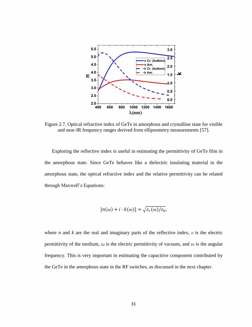
31
Figure 2.7. Optical refractive index of GeTe in amorphous and crystalline state for visible
and near-IR frequency ranges derived from ellipsometry measurements [57].
Exploring the reflective index is useful in estimating the permittivity of GeTe film in
the amorphous state. Since GeTe behaves like a dielectric insulating material in the
amorphous state, the optical refractive index and the relative permittivity can be related
through Maxwell’s Equations:
[𝑛(𝜔) + 𝑖 ∙ 𝑘(𝜔)] = √𝜀𝑟(𝜔)/𝜀0,
where n and k are the real and imaginary parts of the reflective index, ε is the electric
permittivity of the medium, ε0 is the electric permittivity of vacuum, and ω is the angular
frequency. This is very important in estimating the capacitive component contributed by
the GeTe in the amorphous state in the RF switches, as discussed in the next chapter.
32
2.3.2. Phase Transitions between Amorphous and Crystalline States of GeTe
While both the amorphous and crystalline states of GeTe films can be found at room
temperature, phase transitions between the two states can be achieved at elevated
temperatures. As mentioned before, the temperature change during a phase transition
process of phase change materials can be divided into a heating process and a cooling
process. The transition from the amorphous to the crystalline state is known as
crystallization, and the phase transition from the crystalline to the amorphous state is
known as amorphization.
In order for an amorphous GeTe film to experience the crystallization process, the
temperature needs to be elevated for the nucleation process to happen within the film. As
discussed in [54], at an elevated temperature (above the crystallization temperature), the
nucleation process will start to take place within the GeTe film rapidly via multiple
nucleation centers, and eventually expands across the entire volume of the GeTe film.
When the film is cooled down to room temperature, the crystallization process is
complete and the crystalline GeTe film is formed. The crystallization temperature, at
which nucleation happens within the GeTe films, can vary according to factors including
film preparation conditions, substrate properties [54], and GeTe stoichiometric ratio [59].
Most reported crystallization temperatures are above 145°C.
In order to monitor the formation of crystalline structure within the GeTe films during
the crystallization process, an X-ray diffraction (XRD) insitu measurement is commonly
used. Intensity peaks shown in the XRD measurements can indicate the formation of
crystallized structures, and multiple peaks at the same time means multiple crystalline
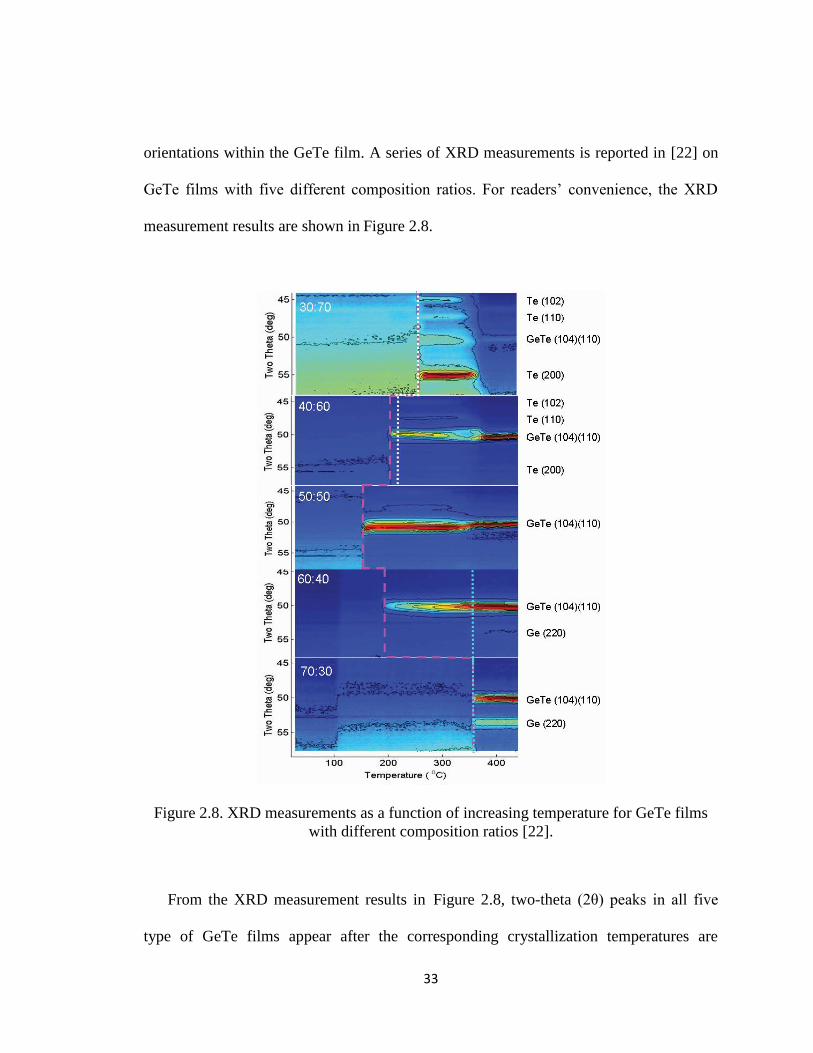
33
orientations within the GeTe film. A series of XRD measurements is reported in [22] on
GeTe films with five different composition ratios. For readers’ convenience, the XRD
measurement results are shown in Figure 2.8.
Figure 2.8. XRD measurements as a function of increasing temperature for GeTe films
with different composition ratios [22].
From the XRD measurement results in Figure 2.8, two-theta (2θ) peaks in all five
type of GeTe films appear after the corresponding crystallization temperatures are

34
reached, which indicate that a certain level of crystalline structure is formed in all GeTe
films. Among these five samples, Ge50Te50 has the lowest crystallization temperature of
approximately 180°C, and Ge70Te30 has the highest crystallization temperature of
approximately 360°C. The crystalline orientations corresponding to each peak are also
listed in the figure, indicating that most GeTe films crystallized through this annealing
process are showing a polycrystalline structure. In the case of Ge50Te50, an initial 2θ peak
at about 50° appears above 180°C, and another sharper peak at the similar angle appears
above 360°C, which could potentially indicate different orientations that have different
crystallization temperatures and coinciding 2θ peaks.
Unlike the crystallization process, the amorphization process of GeTe films take place
under a different annealing temperature profile and has a different mechanism. While it
also requires a heating and a cooling process, the amorphization process of GeTe films
typically needs a higher peak temperature that is well above the crystallization
temperature, and is often preferred to be above the melting temperature of the GeTe film.
The cooling process during amorphization needs to be even faster than that for
crystallization, so that the nucleation process does not have enough time to take place and
after the temperature is quickly dropped back to room temperature, the atoms in the film
are locked in their disordered state, without being able to nucleate unless temperature is
raised again. Thus, the amorphous GeTe film is formed and the amorphization process is
complete. The crystallization time is typically several times slower than the
amorphization time (Figure 2.1).
35
2.3.3. GeTe Fabrication Process for RF Switch Applications
This section will be focused on the results and findings from the GeTe film
preparation process, sample annealing process, as well as other material study
experiments that have been performed here at the University of Michigan. Process
variations play a significant role in the final physical properties of the film. Therefore,
while the results reported in this section is generally in agreement with the results from
reported works summarized in the previous sections, differences in details can be seen.
2.3.3.1. GeTe Film Deposition Process and Basic Electrical Properties
In this work, GeTe films are prepared at the Lurie Nanofabrication Facility (LNF) at
the University of Michigan. The thin-film deposition process of GeTe, both for film
property characterizations and for RF Ohmic switch fabrication, is performed on
passivated silicon substrates. The deposition of GeTe films are done by sputtering using a
Lab 18 Modular Thin Film Deposition System manufactured by Kurt J. Lesker Company.
The sputtering process uses an RF power enabled plasma sputtering source on a single
target of Ge50Te50 alloy, and is performed under a high vacuum chamber condition, with
a base chamber pressure of 3×10⁻⁶ Torr or lower. The RF power used for sputtering varies
from 40 W to 70 W, without the presence of DC voltage bias. The partial pressure during
the sputtering process varies from 3.5 mTorr to 5 mTorr. The sputtering process is done
at room temperature. In order to optimize the sputtering process to obtain GeTe films
with best quality, the base chamber pressure, the RF power and the partial pressure have

36
been varied in the sputtering experiment in order to find a combination that yields the
best result.
The as-sputtered GeTe film is in the amorphous state, with an electrical resistivity
higher than 0.1 Ω∙m. Phase transition from the amorphous to the crystalline state is
achieved by a standard ovenization at 200°C for approximately 30 min. The temperature
ramping rate from room temperature to 200°C is about 6°C/min. After successful
crystallization, the GeTe film exhibits the crystalline state, with an electrical resistivity
lower than 5×10⁻⁵ Ω∙m, which shows an amorphous/crystalline resistivity ratio higher
than 2×10³. Other than the standard ovenization used for crystallization, different
methods have also been characterized to achieve higher effectiveness of phase transition.
Both the GeTe film sputtering process and the crystallization process have been proven to
directly affect the crystalline quality of the GeTe film after the as-deposited amorphous
GeTe is transitioned into crystalline GeTe.
During the GeTe sputtering process, the sputtering speed, or film deposition rate, can
affect the film quality. Generally, a higher deposition rate tends to result in a better film
quality with lower electrical resistivity after crystallization and less introduced impurity
in the film [60]. The measured film deposition rate of GeTe films varies from 0.5 Å/s to
1.8 Å/s, depending on the combinations of sputtering conditions. With the RF sputtering
power varying from 40 W to 70 W, and the partial sputtering pressure between 3.5 mTorr
and 5 mTorr, a series of measured deposition rates are plotted in Figure 2.9. The trend
shows that the combination of a higher power and a lower partial pressure tends to yield a
higher deposition rate. The electrical conductivity of GeTe film samples of the same
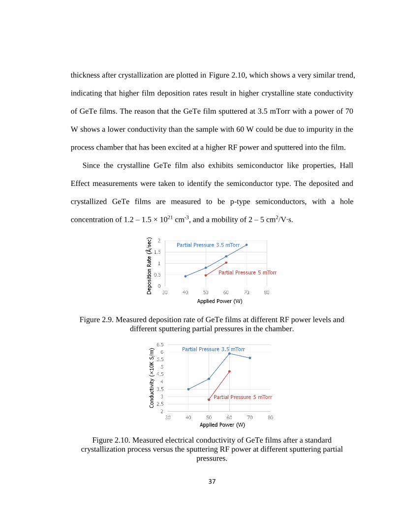
37
thickness after crystallization are plotted in Figure 2.10, which shows a very similar trend,
indicating that higher film deposition rates result in higher crystalline state conductivity
of GeTe films. The reason that the GeTe film sputtered at 3.5 mTorr with a power of 70
W shows a lower conductivity than the sample with 60 W could be due to impurity in the
process chamber that has been excited at a higher RF power and sputtered into the film.
Since the crystalline GeTe film also exhibits semiconductor like properties, Hall
Effect measurements were taken to identify the semiconductor type. The deposited and
crystallized GeTe films are measured to be p-type semiconductors, with a hole
concentration of 1.2 – 1.5 × 1021 cm-3, and a mobility of 2 – 5 cm2/V∙s.
Figure 2.9. Measured deposition rate of GeTe films at different RF power levels and
different sputtering partial pressures in the chamber.
Figure 2.10. Measured electrical conductivity of GeTe films after a standard
crystallization process versus the sputtering RF power at different sputtering partial
pressures.
38
2.3.3.2. GeTe Annealing Process and Crystallization Optimization
The deposited GeTe are annealed using a standard ovenization process. Multiple
samples of GeTe films are tested under the ovenization process with various peak
temperatures to determine the crystallization temperature of the GeTe film. Based on this
study, GeTe starts to crystallize at temperatures above 180°C. While the crystallization
temperature is in good agreement with [22], the electrical conductivity of GeTe measured
after crystallization is about 5 to 10 time lower in many samples, which indicates poor
crystalline film quality. In order to improve the film quality and reduce the electrical
resistivity of crystalline GeTe films, further efforts have been made to optimize the
annealing process parameters, including the annealing temperature, annealing duration
and oven environment (pressure, air/N2 gas, etc.). It has been found out that a low-
pressure annealing process (< 250 mTorr) with a N2 based oven environment tends to
result in the best crystalline GeTe film quality. This is possibly because in air, GeTe is
prone to oxidization, which results in the formation of nano-crystalline structures
consisting of GeOx and TeOx. The reduced oven pressure also contributes to reduced
chance of oxidization.
After the optimal oven conditions for GeTe crystallization has been characterized, the
crystallization temperature is determined by comparing the quality of GeTe film samples
crystallized with different crystallization temperatures under the same oven condition
described above. From the lowest crystallization temperature of 180°C that has been
observed to be able to crystallize the GeTe films, temperature is varied from 180°C to
350°C. All of the GeTe film samples are annealed in a 250 mTorr low-pressure N2
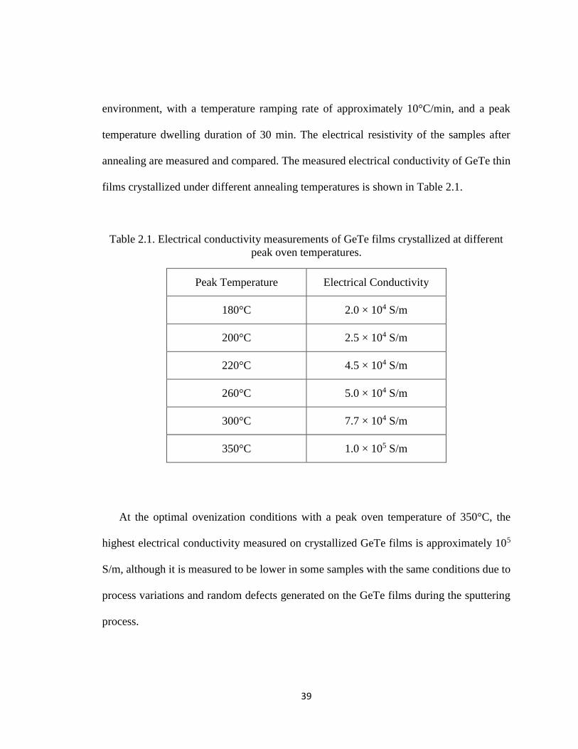
39
environment, with a temperature ramping rate of approximately 10°C/min, and a peak
temperature dwelling duration of 30 min. The electrical resistivity of the samples after
annealing are measured and compared. The measured electrical conductivity of GeTe thin
films crystallized under different annealing temperatures is shown in Table 2.1.
Table 2.1. Electrical conductivity measurements of GeTe films crystallized at different
peak oven temperatures.
Peak Temperature Electrical Conductivity
180°C 2.0 × 10⁴ S/m
200°C 2.5 × 10⁴ S/m
220°C 4.5 × 10⁴ S/m
260°C 5.0 × 10⁴ S/m
300°C 7.7 × 10⁴ S/m
350°C 1.0 × 10⁵ S/m
At the optimal ovenization conditions with a peak oven temperature of 350°C, the
highest electrical conductivity measured on crystallized GeTe films is approximately 105
S/m, although it is measured to be lower in some samples with the same conditions due to
process variations and random defects generated on the GeTe films during the sputtering
process.
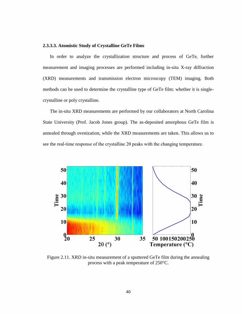
40
2.3.3.3. Atomistic Study of Crystalline GeTe Films
In order to analyze the crystallization structure and process of GeTe, further
measurement and imaging processes are performed including in-situ X-ray diffraction
(XRD) measurements and transmission electron microscopy (TEM) imaging. Both
methods can be used to determine the crystalline type of GeTe film: whether it is single-
crystalline or poly crystalline.
The in-situ XRD measurements are performed by our collaborators at North Carolina
State University (Prof. Jacob Jones group). The as-deposited amorphous GeTe film is
annealed through ovenization, while the XRD measurements are taken. This allows us to
see the real-time response of the crystalline 2θ peaks with the changing temperature.
Figure 2.11. XRD in-situ measurement of a sputtered GeTe film during the annealing
process with a peak temperature of 250°C.

41
Figure 2.12. XRD in-situ measurement of a sputtered GeTe film during the annealing
process with a peak temperature of 550°C.
The XRD in-situ measurements results with a peak ovenization temperature of 250°C
and 500°C are shown in Figure 2.11 and Figure 2.12, respectively. Figure 2.11 shows that
as the temperature ramps up from room temperature to 250°C, a dominating 2θ peak at
approximately 30° appears when the temperature reaches 220°C (at 13 min), but several
other peaks at different 2θ angles are also showing as the temperature rises. The second
XRD measurement (shown in Figure 2.12) with a higher annealing temperature on a
crystalline GeTe indicates that when the temperature reaches about 350°C, the XRD peak
at 2θ = 30° is slightly twisted with an increased sharpness. This measurement also
indicates that 550°C is not sufficiently high to completely melt GeTe and remove all
crystalline sites. The multiple peaks in XRD measurement results indicate that the GeTe
film samples deposited and annealed under the conditions discussed above are showing a
poly-crystalline structure, with multiple crystalline orientations within the same sample.
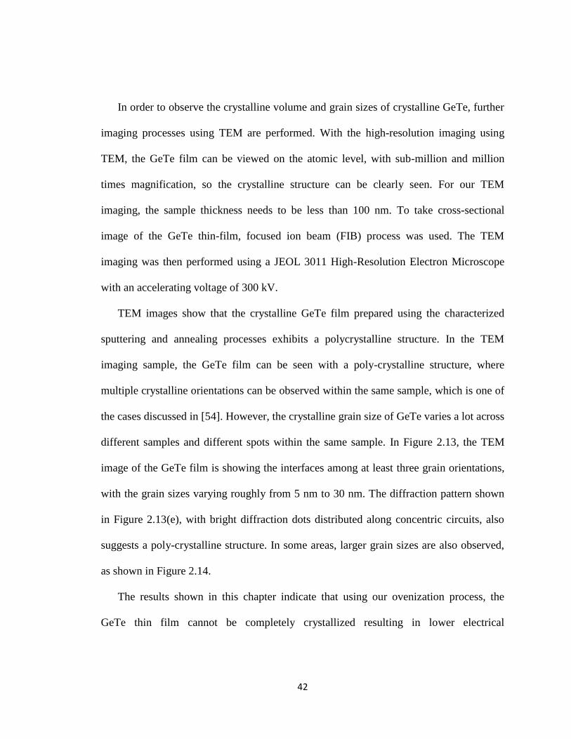
42
In order to observe the crystalline volume and grain sizes of crystalline GeTe, further
imaging processes using TEM are performed. With the high-resolution imaging using
TEM, the GeTe film can be viewed on the atomic level, with sub-million and million
times magnification, so the crystalline structure can be clearly seen. For our TEM
imaging, the sample thickness needs to be less than 100 nm. To take cross-sectional
image of the GeTe thin-film, focused ion beam (FIB) process was used. The TEM
imaging was then performed using a JEOL 3011 High-Resolution Electron Microscope
with an accelerating voltage of 300 kV.
TEM images show that the crystalline GeTe film prepared using the characterized
sputtering and annealing processes exhibits a polycrystalline structure. In the TEM
imaging sample, the GeTe film can be seen with a poly-crystalline structure, where
multiple crystalline orientations can be observed within the same sample, which is one of
the cases discussed in [54]. However, the crystalline grain size of GeTe varies a lot across
different samples and different spots within the same sample. In Figure 2.13, the TEM
image of the GeTe film is showing the interfaces among at least three grain orientations,
with the grain sizes varying roughly from 5 nm to 30 nm. The diffraction pattern shown
in Figure 2.13(e), with bright diffraction dots distributed along concentric circuits, also
suggests a poly-crystalline structure. In some areas, larger grain sizes are also observed,
as shown in Figure 2.14.
The results shown in this chapter indicate that using our ovenization process, the
GeTe thin film cannot be completely crystallized resulting in lower electrical
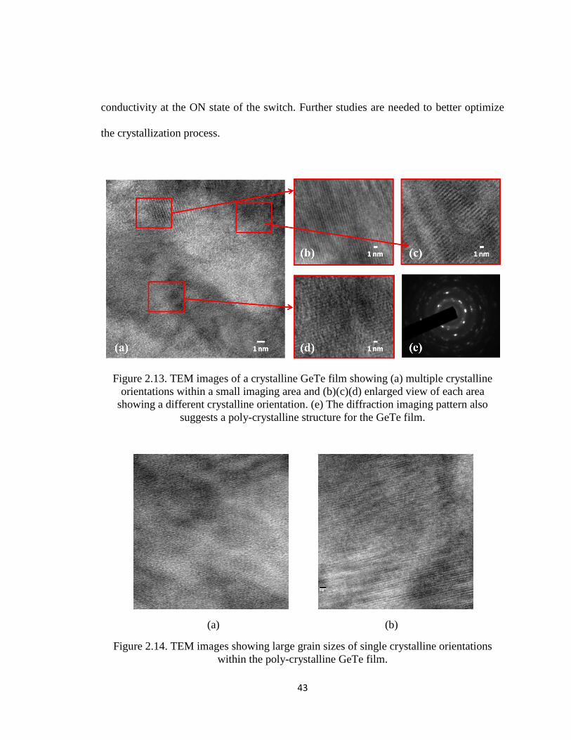
43
conductivity at the ON state of the switch. Further studies are needed to better optimize
the crystallization process.
Figure 2.13. TEM images of a crystalline GeTe film showing (a) multiple crystalline
orientations within a small imaging area and (b)(c)(d) enlarged view of each area
showing a different crystalline orientation. (e) The diffraction imaging pattern also
suggests a poly-crystalline structure for the GeTe film.
(a) (b)
Figure 2.14. TEM images showing large grain sizes of single crystalline orientations
within the poly-crystalline GeTe film.
44
CHAPTER 3 GeTe Phase Change Material Based RF Ohmic Switches
As discussed in the previous chapter, GeTe films have been proven to possess a low-
resistivity crystalline state and a high-resistivity amorphous state at room temperature,
and phase transitions between these two states are achievable with thermal actuation at a
fast speed. Optical storage applications using GeTe have also demonstrated good
reliability of GeTe film. Therefore, GeTe is a strong candidate for RF switching
applications. In phase change material-based RF switches using GeTe or GST materials
in general, the core structure is the phase change material via connecting two or more RF
terminals to form the switch connection. In order to achieve phase transitions for
switching activities, thermal actuation structures need to be designed along with the RF
switching element. The most commonly used methods for thermal actuation include laser
induction [28] [29], and joule heating using a heating current drawn through a resistive
heater. The latter is a more popular way for RF switch designs, and will be talked about
in detail in this chapter.

45
3.1. Early Designs of Phase Change Material Based RF Switches
3.1.1. RF Switches Using Different Phase Change Materials
One of the earliest proposed designs of phase change RF switches uses Ge2Sb2Te5 via
as the switching element, and a lateral heater path through the via as the thermal actuation
conduit [36]. In this design, the two switch terminals are vertically connected by the GST
via and the prototype device is fabricated in a standard 180-nm CMOS copper back-end
technology. As one of the earliest proof-of-concept designs of an Ohmic switch using
phase change materials, this work has reported successful phase transitions of the GST
material and showed switching activities of the device for up to 100 switching cycles
with a stable OFF/ON DC resistance ratio of over 200. In the ON state, the DC resistance
of the switch was approximately 5 kΩ, which is very high for most applications. The high
ON-state resistance is due to the material properties of Ge2Sb2Te5, which has a relatively
high crystalline state resistivity. While this is acceptable in memory-related applications
as long as the amorphous-crystalline resistivity ratio is high and stable, it creates great
limitations in RF switch designs. For this reason, alternative phase change materials such
as GeSb and GeTe have been investigated for designing Ohmic switches. A novel three-
terminal phase change switch design has been reported using Ge50Sb50, or GeSb as the
switching element [52]. The GeSb electronic switches are demonstrated in a
reconfigurable inductor design where the GeSb switches are used to reconfigure the
inductance value. In this reported work, the switches use the structure where lateral metal
electrodes are connected by the GeSb vias, and through switching activities, the
46
integrated spiral shaped inductor is reconfigured into different inductance values. In order
to reduce the via size of each individual GeSb via, this design uses a parallel array
configuration of multiple GeSb vias, which reduces the required switching current level.
The phase transitions of GeSb are measured to be stable with an OFF/ON resistance ratio
of approximately 100. This work provided the idea of a novel structure for phase change
switch design that requires a switching power level that is more acceptable in many
integrated systems.
Among different phase change materials, a low crystalline state resistivity is much
preferred in Ohmic switch designs, as it is the key to achieve a low ON-state insertion
loss and therefore a better performance. Compared to the two phase change switch
designs discussed above using Ge2Sb2Te5 and GeSb, another proposed design of phase
change switch using GeTe has shown much lower ON-state resistance and a much higher
switch isolation [53]. The improved performance of this design is mostly because of the
material properties of GeTe. The GeTe film deposited and measured in [53] is reported to
have a crystalline state resistivity of 4×10⁻⁶ Ω∙m, and an amorphous state resistivity of 76
Ω∙m, showing an amorphous-crystalline state resistivity ratio of 1.9×10⁷. The switch uses
a vertical RF connection structure, with a top and a bottom electrode connected through
the GeTe via, and the via area is defined by a SiO2 layer patterned through etching. The
switch after fabrication is measured to have an ON-state resistance of 180 Ω and an OFF-
state resistance of approximately 1.3 MΩ, showing an OFF/ON resistance ratio of 7×10³
for the switch, which is a significant performance improvement compared to the designs
reported in [36] and [52].

47
Early designs of phase change material switches, especially GeTe-based switches
have shown their great potential in RF switching applications. Compared to solid-state
based RF switches using different technologies, such as bulk-Si, SOI, SOS, pHEMT, etc.,
phase change material based switches have the advantage of lower ON state resistance
and higher linearity, as will be shown in this chapter. Since the reported works discussed
above, efforts have been made to build phase change RF switches with improved
performance that is comparable to or better than other switch technologies.
3.1.2. Low-Loss Two-Terminal GeTe Based RF Switch
The switch designs discussed above have proven good functionality of phase change
materials in switching applications, but the reported performance parameters such as
insertion loss are not competitive compared to existing switch designs. Improving the
performance is critical for phase change material based switches to show their advantages
against other types of switches, especially in reconfigurable RF applications. A two-
terminal RF Ohmic switch using GeTe has since been proposed, showing very low loss
across a wide frequency range [61]. The cross-sectional schematic of the GeTe RF switch
proposed in [61] is shown in Figure 3.1 for easier understanding of the structure.
Figure 3.1. Cross-sectional schematic of the two-port GeTe-based RF switch [61].
48
This two-port switch uses a vertical connection of two metal electrodes as the two
terminals. These two terminals are responsible for both RF signal transmission and GeTe
thermal actuation for phase transitions. The GeTe connection via area between the top
and bottom electrodes is defined by the SiO2 interlayer patterned through plasma etching.
When the GeTe via is in the crystalline state, the insertion loss of the switch is mainly
determined by the electrical resistivity of the GeTe film and the dimensions of the
connection via. Since the resistivity of crystalline GeTe and the film thickness are fixed
by the fabrication process, the sizing of the connection via area is used to balance the
ON-state insertion loss and OFF-state isolation.
For a lower insertion loss when the switch is turned on, it is preferred to have a larger
GeTe via area connecting the two RF terminals. However, a larger area will result in a
slower switching speed due to the increased volume of GeTe that needs to go through the
phase transitions. Therefore, an alternative structure of multiple GeTe via connections is
also proposed in this work, where the RF terminals are connected by multiple GeTe vias
in parallel with each GeTe via having a small area. This structure results in both a low
insertion loss and a fast switching speed. The SEM images in Figure 3.2 show the
examples of the GeTe based RF switches with a single-via and a multi-via configuration.

49
(a) (b)
Figure 3.2. SEM images of the GeTe-based RF switches reported in [61] with (a) a single
3m×3m via configuration and (b) a multi-via configuration with five 2m×2m vias
connected in parallel [61].
(a) (b)
Figure 3.3. Measured resistance of GeTe RF switches with a single-via and multi-via
configurations from DC to 3 GHz when the GeTe via is at the (a) crystalline state and (b)
amorphous state [61].
Figure 3.4. Measured intrinsic capacitance of the GeTe RF switches when the GeTe is at
the amorphous state.
0.0 0.5 1.0 1.5 2.0 2.5 3.00.0
0.5
1.0
1.5
2.0
2.5
3.0
Re
sis
tan
ce
(
)
Frequency (GHz)
Single 3x3m2 via
Five 2x2m2 vias
0.0 0.5 1.0 1.5 2.0 2.5 3.00
2
4
6
8
10
Re
sis
tan
ce
(k
)
Frequency (GHz)
Single 3x3m2 via
Five 2x2m2 vias
0.0 0.5 1.0 1.5 2.0 2.5 3.00
20
40
60
80
100
Cap
acit
an
ce (
fF)
Frequency (GHz)
Single 3x3m2 via
Five 2x2m2 vias

50
The measured resistances of the switches with the single-via and multi-via
configurations at the GeTe crystalline and amorphous states are shown in Figure 3.3, and
the measured capacitances of the switches when the GeTe is at the amorphous state is
shown in Figure 3.4. When the switch is turned ON with GeTe at the crystalline state, the
low resistance between the two RF terminals determines the insertion loss, and when the
switch is turned OFF with GeTe at the amorphous state, although the resistance of the
switch is much higher, capacitance across the terminals becomes dominant in the
isolation, especially at higher frequencies. The measured scattering (S)-parameters of the
switch with the single-via configuration in both the ON and OFF states are shown in
Figure 3.5, which show competitive insertion loss and isolation of this type of switch
design compared to other existing technologies.
(a) (b)
Figure 3.5. Measured and de-embedded S11 and S21 of the GeTe RF switch with the
single-via configuration (a) at the crystalline and (b) amorphous states of GeTe.
0 5 10 15 20 25-80
-60
-40
-20
0
Measured S21
De-embedded S21
Measured S11
De-embedded S11
S-p
ara
me
ters
(d
B)
Frequency (GHz)
0 5 10 15 20 25-80
-60
-40
-20
0
S-P
ara
mete
rs (
dB
)
Frequency (GHz)
Measured S21
De-embedded S21
Measured S11
De-embedded S11

51
In this two-terminal switch structure, the RF signal path and the heating path share
the same two terminals. However, the requirements for the terminals used for RF signal
transmissions and thermal actuations are very different. For RF signal transmissions, it is
preferred to have low-resistance metal electrodes for good loss performance, but for
thermal actuations, the heating path needs to have a high resistance level. Therefore, the
two-terminal structure has a limited performance as both heating and RF structures
cannot be optimized simultaneously. To deal with this problem, we have proposed four-
terminal structures with two RF terminals and two separate heating terminals.
3.2. Four-Terminal GeTe RF Switches
The four-terminal structure of GeTe-based RF switches is intended to separate the
thermal actuation signal path from the RF path. With the RF signal path and the heating
path separated, it is possible to separately design the two paths to be optimal for each
function. An early proposed design of a four-terminal GeTe-based RF switch is reported
in [62] and later in [63]. This four-terminal RF switch uses an inline structure with the
two RF terminals laterally connected by the GeTe via whose size is defined by directly
patterning the GeTe film. The two heating terminals are connected through a resistive
heater path that is electrically isolated from the RF signal path. Thermal actuation is
achieved by drawing heating current from the heater path to heat up the GeTe via through
thermal coupling. In this design, only the RF terminals are in direct contact with the
GeTe via, which reduces the parasitics associated with the heater terminals and both the
performance and reliability are improved from previous designs.

52
With the similar idea in mind, we have proposed a novel phase change RF switch
design having four terminals. In this section, two different structures of four-terminal
GeTe RF switches will be discussed. Their design procedures, structures, fabrication
processes, and performance will be discussed in detail. A comparison between the two
structures will also be presented.
3.2.1. Four-Terminal GeTe RF Switch with Direct Heating Scheme
The directly heated switch structure, similar to the one in [62], has four terminals, two
RF ports and two for Joule heating. The most significant difference between the in-line
four terminal structure in [62] and our design is that in the directly heated switch, the
heating current is drawn through the GeTe via itself to achieve phase transitions. This
design offers a higher heating efficiency compared to the design with a separated heater
in [62]. The directly heated phase change switch design was first published in [64], with a
brief discussion of the working principle, structure, fabrication process, and the
performance evaluation. The structure and fabrication process were then slightly
modified for an improved performance and the results were then reported in [65]. This
structure is similar to the one reported in [36], where a resistive heater is placed through
the GST via, but in this design the GeTe via is not in a simple pillar or via shape, but
instead has been designed into a more complicated structure considering the functionality,
thermal actuation effectiveness, and RF performance [66]. Details about the GeTe RF
switch with direct heating scheme will be discussed in this sub-section.
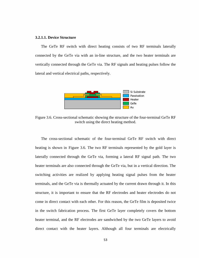
53
3.2.1.1. Device Structure
The GeTe RF switch with direct heating consists of two RF terminals laterally
connected by the GeTe via with an in-line structure, and the two heater terminals are
vertically connected through the GeTe via. The RF signals and heating pulses follow the
lateral and vertical electrical paths, respectively.
Figure 3.6. Cross-sectional schematic showing the structure of the four-terminal GeTe RF
switch using the direct heating method.
The cross-sectional schematic of the four-terminal GeTe RF switch with direct
heating is shown in Figure 3.6. The two RF terminals represented by the gold layer is
laterally connected through the GeTe via, forming a lateral RF signal path. The two
heater terminals are also connected through the GeTe via, but in a vertical direction. The
switching activities are realized by applying heating signal pulses from the heater
terminals, and the GeTe via is thermally actuated by the current drawn through it. In this
structure, it is important to ensure that the RF electrodes and heater electrodes do not
come in direct contact with each other. For this reason, the GeTe film is deposited twice
in the switch fabrication process. The first GeTe layer completely covers the bottom
heater terminal, and the RF electrodes are sandwiched by the two GeTe layers to avoid
direct contact with the heater layers. Although all four terminals are electrically

54
connected to the GeTe via, a high resistive material is used for the heater layers to ensure
good isolation between the RF signals and the heating pulses, and also to maximize the
heating efficiency. The RF terminals, on the other hand, are designed with very low
resistance for good loss performance of the switch.
The design of the heating terminals in this type of GeTe switch is critical to obtain
both good heating effectiveness and minimal interference with RF signal transmission. In
terms of resistance, the heater path needs to be designed with good impedance matching
to get to heat delivery to the GeTe via. In the meantime, since the RF electrodes are in
indirect contact with the heater electrodes through the GeTe layer, the heaters also need
to have a high enough resistance to ensure good isolation between the two paths in order
to minimize the heating pulse interference to RF signals. This essentially limits the
choices of material for heater paths. In the initial designs, titanium nitride (TiN) was used
as the resistive heater material, which was also proven to be a very effective and reliable
choice. The TiN film is a metal-like ceramic material, which has a much higher resistivity
than most conductive metals, but can be used as resistors. It has also been tested with
good stability at high temperatures.
(a) (b)
Figure 3.7. (a) Top-view layout of the heater path in the GeTe switch and its material
combinations. (b) Simplified equivalent circuit model of the heater path.

55
The layout of the heater path in the GeTe RF switch with direct heating scheme and
its simplified equivalent circuit model are shown in Figure 3.7. In Figure 3.7(b), resistor
R1 represents the vertical resistance of GeTe, which varies between the crystalline and
amorphous states. Resistors R2 represent the TiN sections of the heater path, which are
next to and in direct contact with the GeTe via. Finally, resistors R3 are the resistance of
each DC pad covered with gold. From modeling and simulation, the value of R1 (GeTe
resistance) is smaller than 5 Ω at the crystalline state, and is above 5 kΩ at amorphous
state. R3 is within 5 Ω as gold is a good conductor. R2 is designed to be greater than 0.5
kΩ. Therefore, when GeTe is at crystalline state, the resistance along the heater path is
concentrated at the TiN sections, ensuring that the heat is effectively delivered to the
GeTe via. When GeTe is at the amorphous state, R1 becomes the dominant resistance,
and the resistance of TiN (R2) serves as protection for GeTe, so that once GeTe is back to
the crystalline state, most power is dissipated in the TiN sections and GeTe is not
accidentally heated back to the amorphous state. The basic heater path structure used in
directly heated switches is the one shown in Figure 3.7, but the sizing, material choice
and fabrication process have been modified slightly as the switch design was matured.
To verify the required conditions for Joule heating of GeTe, thermal simulations are
performed using COMSOL multi-physics FEA simulation tool. As previously discussed,
to convert GeTe from crystalline to amorphous state, the Joule heating temperature
should rise above the GeTe melting point. Heat dissipation to the substrate needs to be
rapid enough, so the atoms in the GeTe layer cannot nucleate and re-crystallize. Thus,
GeTe should have good thermal coupling to the substrate. In order to achieve phase

56
transition from the amorphous state back to the crystalline state, lower power needs to be
applied. The temperature must rise above the crystallization temperature of 250°C or
higher, while remaining below the melting temperature. The switch should cool down
gradually by slow removal of the heating current to convert the via back to the crystalline
state. In COMSOL simulations, is the crystallization and amorphization conditions are
realized by applying appropriate heating pulses, and the thermal responses are shown in
Figure 3.8. It is shown that both crystallization and amorphization requirements are met
with the heater design.
(a) (b)
Figure 3.8. COMSOL simulation for Joule heating conditions of the GeTe switch. (a) For
GeTe crystallization, a voltage pulse with an amplitude of 7 V is applied for a duration of
2 µs, and the maximum temperature at the GeTe volume reaches 310 °C. (b) For GeTe
amorphization, a voltage pulse with an amplitude of 12.5 V is applied for a duration of
1s, and the maximum temperature at the GeTe volume is above 710 °C. The simulation
results verify that the heating conditions meet the requirements for GeTe phase
transitions.

57
3.2.1.2. Fabrication Process
The fabrication process of the GeTe RF switch with direct heating is performed on a
silicon substrate, passivated with a dielectric layer. Throughout the development process,
silicon substrates with different quality and properties have been used. Based on the
measurement results from devices fabricated on different substrates, it is believed that the
doping type of the silicon substrate does not affect the quality of the fabricated devices
significantly. However, devices on a high resistivity substrate is found to have improved
performance at high frequencies compared to those on a substrate with low resistivity.
For example, a device fabricated on a 1000 Ω∙cm silicon substrate is measured to perform
better than a device fabricated on a 30 Ω∙cm silicon substrate having an insertion loss that
is lower by a few dB at frequencies over 1 GHz. In the measurement process, however,
the performance degradation caused by substrate loss can be de-embedded based on
reference devices. Details about the measurement process will be discussed later.
Details of the fabrication process of the GeTe switches have been repeatedly modified
in terms of both material choice and process flow in order to improve the overall device
quality, but a general fabrication process flow is shown in Figure 3.9.
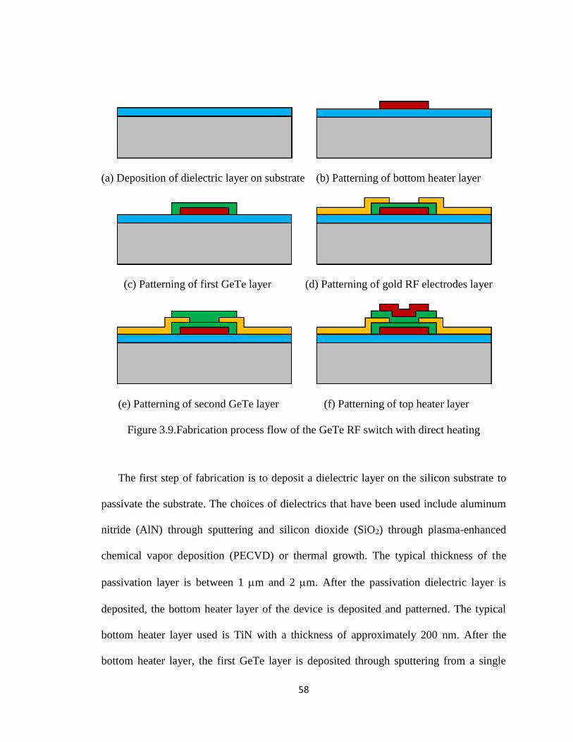
58
(a) Deposition of dielectric layer on substrate (b) Patterning of bottom heater layer
(c) Patterning of first GeTe layer (d) Patterning of gold RF electrodes layer
(e) Patterning of second GeTe layer (f) Patterning of top heater layer
Figure 3.9.Fabrication process flow of the GeTe RF switch with direct heating
The first step of fabrication is to deposit a dielectric layer on the silicon substrate to
passivate the substrate. The choices of dielectrics that have been used include aluminum
nitride (AlN) through sputtering and silicon dioxide (SiO2) through plasma-enhanced
chemical vapor deposition (PECVD) or thermal growth. The typical thickness of the
passivation layer is between 1 m and 2 m. After the passivation dielectric layer is
deposited, the bottom heater layer of the device is deposited and patterned. The typical
bottom heater layer used is TiN with a thickness of approximately 200 nm. After the
bottom heater layer, the first GeTe layer is deposited through sputtering from a single

59
GeTe target, as discussed in the previous chapter. The thickness of the GeTe layer is
about 100 nm. The patterned GeTe layer needs to completely cover the bottom heater
layer in order to prevent any direct contact between the heater line and the RF electrodes,
which are deposited after the GeTe layer. After the gold RF electrode layer with a
thickness of 200 nm is patterned, the second GeTe layer is deposited with the same
pattern as the first GeTe layer. The two GeTe layers form a sandwiching structure against
the RF electrodes. The second GeTe layer also has a thickness of about 100 nm, giving a
total thickness of 200 nm at the via area. Finally, a top heater layer of 200 nm TiN is
patterned to form the heating signal path. After the major steps, an additional gold layer
patterning is performed on both the RF and heater terminals to reduce the resistance of
the heater and RF pads. A top passivation layer is also deposited in some batches of
devices as a protection layer, and also for performance comparison.
In this fabrication process, all non-dielectric layers are patterned through lift-off. A
photoresist layer is built with patterns created by photo-lithography before the layer
deposition. A standard photoresist lift-off process is performed after the deposition with
an overnight acetone treatment, followed by an acetone-IPA-deionized (DI) water
cleaning cycle while applying an ultrasonic agitation. The sample is finally rinsed with
DI water and dried with compressed N2 gas.
After patterning of each GeTe layer, it is preferred to immediately perform the
annealing process for GeTe crystallization, since the as-deposited GeTe film is
amorphous, as previously discussed. The annealing process is generally performed in a
convection oven at a temperature of at least 220°C for good crystallization results. In
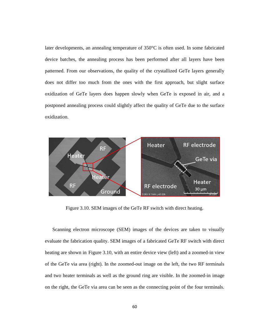
60
later developments, an annealing temperature of 350°C is often used. In some fabricated
device batches, the annealing process has been performed after all layers have been
patterned. From our observations, the quality of the crystallized GeTe layers generally
does not differ too much from the ones with the first approach, but slight surface
oxidization of GeTe layers does happen slowly when GeTe is exposed in air, and a
postponed annealing process could slightly affect the quality of GeTe due to the surface
oxidization.
Figure 3.10. SEM images of the GeTe RF switch with direct heating.
Scanning electron microscope (SEM) images of the devices are taken to visually
evaluate the fabrication quality. SEM images of a fabricated GeTe RF switch with direct
heating are shown in Figure 3.10, with an entire device view (left) and a zoomed-in view
of the GeTe via area (right). In the zoomed-out image on the left, the two RF terminals
and two heater terminals as well as the ground ring are visible. In the zoomed-in image
on the right, the GeTe via area can be seen as the connecting point of the four terminals.
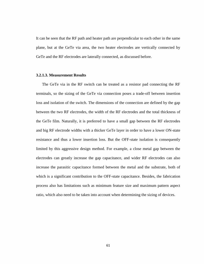
61
It can be seen that the RF path and heater path are perpendicular to each other in the same
plane, but at the GeTe via area, the two heater electrodes are vertically connected by
GeTe and the RF electrodes are laterally connected, as discussed before.
3.2.1.3. Measurement Results
The GeTe via in the RF switch can be treated as a resistor pad connecting the RF
terminals, so the sizing of the GeTe via connection poses a trade-off between insertion
loss and isolation of the switch. The dimensions of the connection are defined by the gap
between the two RF electrodes, the width of the RF electrodes and the total thickness of
the GeTe film. Naturally, it is preferred to have a small gap between the RF electrodes
and big RF electrode widths with a thicker GeTe layer in order to have a lower ON-state
resistance and thus a lower insertion loss. But the OFF-state isolation is consequently
limited by this aggressive design method. For example, a close metal gap between the
electrodes can greatly increase the gap capacitance, and wider RF electrodes can also
increase the parasitic capacitance formed between the metal and the substrate, both of
which is a significant contribution to the OFF-state capacitance. Besides, the fabrication
process also has limitations such as minimum feature size and maximum pattern aspect
ratio, which also need to be taken into account when determining the sizing of devices.

62
Figure 3.11. Simplified top view of the RF electrode connection through GeTe via
showing how the dimensions of the connection are defined.
A simplified top view of the GeTe via area of the switch is shown in Figure 3.11 for
easier understanding. If the GeTe via is treated as a block of resistor, the RF electrode
gap distance will define the length of the resistor, and the RF electrode width will define
the width. The height of the resistor is defined by the total thickness of GeTe. In the
actual structure of the device, the GeTe layer has a larger area for overlapping with and
sandwiching the RF electrodes, and thus additional fringing effects, contact resistance,
and parasitics need to be considered as well. For a more accurate sizing evaluation,
electromagnetic simulations are performed using ANSYS HFSS to predict the insertion
loss and isolation of the switch with different sizing parameters. In a sample series of
simulations, the thickness of the GeTe layer is set to be either 100 nm or 200 nm, and the
RF electrode gap is varied among 0.25 m, 0.5 m, and 1 m. The width of RF
electrodes is fixed at 20 m for fewer combinations, but in the case of actual fabrication,
the RF electrode width is varied across devices to evaluate the design trade-off.
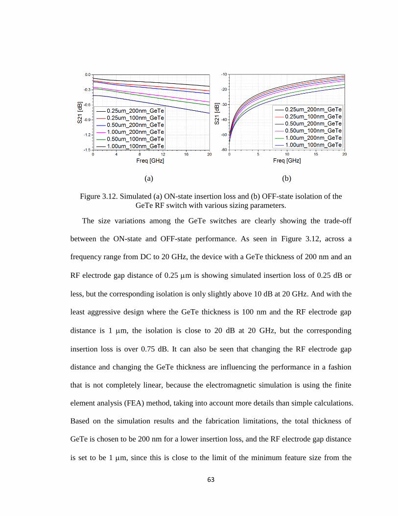
63
(a) (b)
Figure 3.12. Simulated (a) ON-state insertion loss and (b) OFF-state isolation of the
GeTe RF switch with various sizing parameters.
The size variations among the GeTe switches are clearly showing the trade-off
between the ON-state and OFF-state performance. As seen in Figure 3.12, across a
frequency range from DC to 20 GHz, the device with a GeTe thickness of 200 nm and an
RF electrode gap distance of 0.25 m is showing simulated insertion loss of 0.25 dB or
less, but the corresponding isolation is only slightly above 10 dB at 20 GHz. And with the
least aggressive design where the GeTe thickness is 100 nm and the RF electrode gap
distance is 1 m, the isolation is close to 20 dB at 20 GHz, but the corresponding
insertion loss is over 0.75 dB. It can also be seen that changing the RF electrode gap
distance and changing the GeTe thickness are influencing the performance in a fashion
that is not completely linear, because the electromagnetic simulation is using the finite
element analysis (FEA) method, taking into account more details than simple calculations.
Based on the simulation results and the fabrication limitations, the total thickness of
GeTe is chosen to be 200 nm for a lower insertion loss, and the RF electrode gap distance
is set to be 1 m, since this is close to the limit of the minimum feature size from the

64
lithography, and any smaller size may cause pattern quality and yield issues. Throughout
the development process, the sizing has been slightly modified to better address the
fabrication process characterization results.
In the fabrication process, the metal contact pads are integrated with the GeTe RF
switch for RF and DC measurement purposes. As seen in Figure 3.10(a), the terminal
pads and the ground ring form coplanar waveguide (CPW) transmission lines are
connected to the switch for RF measurements. A pair of air-coplanar (ACP) RF probes
with the ground-signal-ground (GSG) configuration is used for the two-port scattering
parameters measurements to evaluate the insertion loss and isolation. The thermal
actuation for switching activities is achieved by applying a DC voltage pulse generated
from a waveform signal generator and delivered by two DC probes connected to the two
heater terminal pads.
(a) (b)
Figure 3.13. Measured (de-embedded) and simulated RF response of the GeTe RF switch.
(a) Insertion loss at the ON-state. (b) Isolation at the OFF-state.
65
RF measurements are performed using Cascade ACP probes landed on the RF
terminal pads of the device, and the RF signal transmission S-parameters are measured
with the Agilent N5242 PNA-X network analyzer. The on-wafer measurement results
have been de-embedded using a reference device from the same wafer in order to
eliminate inaccuracy caused by probe contact and measurement setup. Electromagnetic
simulation results acquired using ANSYS HFSS are also included for comparison. The
measured S21 parameters at the ON-state and OFF-state are shown in Figure 3.13. In
simulations, the electrical conductivity of GeTe in crystalline state is set to 5×10⁴ S/m,
while its amorphous state conductivity is set to 1 S/m. The discrepancy between
measurements and simulations are mostly due to a lower OFF/ON resistance ratio
achieved in the fabrication as well as other effects that are not taken into account by the
simulation. From the measurement results, the GeTe RF switch with direct heating
scheme shows an insertion loss of less than 0.5 dB and an isolation over 18 dB from DC
to 20 GHz, which indicates very competitive performance compared to other existing
types of RF switches such as MEMS and solid-state switches.
In order to better analyze the performance and illustrate how the RF response is
affected by the resistive and reactive elements from the switch and the external circuits,
an equivalent electrical model is developed. For the GeTe switch with the direct heating
method, the equivalent circuit is shown in Figure 3.14.

66
Figure 3.14. Equivalent circuit model of the four-terminal GeTe RF switch with direct
heating. The circuit elements shown in the model include resistive and reactive parts from
the components of the GeTe switch and the external metal routing as well as the
measurement setup.
This model was first proposed by us in [65]. Based on the specific material properties
of phase change material, the GeTe via is essentially modeled as a parallel connection of
a resistor, a capacitive component, and a series R-C connection to simulate the RF
response. Since both the two RF terminals and the two heater terminals are connected to
the GeTe via through a lateral and a vertical path, respectively, additional resistive
components are used to model the electrical connections among the terminals. The
resistors RI, RI2 and RI3 represent the resistance from different portions of GeTe, and RH
represents the resistance from the heater, which is in contact with GeTe. The parallel
capacitance of the GeTe pad is modeled by CI. Since the GeTe is in direct contact with
both the RF and the heater terminals, it is divided into multiple elements. Along the RF
path from Port 1 to Port 2, several parallel paths exist: Path 1 connects the two RF lines
through GeTe laterally (RI3); Paths 2 and 3 are due to the overlap of RF signal line with
the heater line through vertical GeTe resistance (RI2). Here, RH models the lateral
67
resistance of the heater line. Along the RF path, there is also a feed-through capacitance,
modeling the lateral capacitance of GeTe (CI2). Along the heating path, the main
elements are the resistive components of the heater and the GeTe via that is vertically
connecting the two heater terminals. Additional connections between the heater terminals
exist because they are also in contact with the RF signal paths, but those connections
have much higher impedance so they have a smaller effect in comparison. All the
resistive components that represent the portions of the GeTe vias have a variable
resistance switching between the crystalline and amorphous states. In addition to the
GeTe switch, there are parasitic elements from the metal RF transmission lines as well as
the measurement setup. The resistive component RS and inductive component LS
represent small parasitics from the RF probes and cables that are not calibrated out. The
capacitive component CP models the small parallel-plate capacitor formed by the
deposited gold metal lines and the substrate with the passivation layer in between.
When the GeTe switch is turned on, the GeTe is in the crystalline state with low
resistivity, and the switch impedance is determined primarily by the resistance through
the RF terminals. When the switch is turned off, the GeTe is in the amorphous state with
much higher resistivity. The switch impedance, especially at higher frequencies, is
greatly dependent on the capacitance that the GeTe via creates. Based on the
measurements, the GeTe thin film offers a resistivity of roughly 0.015 – 0.02 Ω∙mm in
the crystalline state, and 0.5 – 0.7 Ω∙m in the amorphous state. As mentioned before, the
devices have size variations across each wafer. The sample used for measurements and
RF performance evaluation has an RF electrode width of 20 m and an RF electrode gap

68
distance of 1 m (the actual gap distance measured from fabricated devices was close to
0.9 m due to feature accuracy of the lithography process). The extracted values of
elements from Figure 3.14 are used to determine the figure-of-merit cut-off frequency of
the device, which is defined by 𝑓𝑐𝑜 = 1/(2 ∙ 𝜋 ∙ 𝑅𝑂𝑁 ∙ 𝐶𝑂𝐹𝐹). When the switch is turned
ON, the resistance from the RF terminals is 𝑅𝑂𝑁 ≈ 4.8 Ω, and when it is turned OFF, the
capacitance from the RF terminals is 𝐶𝑂𝐹𝐹 ≈ 8 fF. Therefore, the switch has a cut-off
frequency of over 4 THz. Later designs of the switch have improved performance and a
higher cut-off frequency.
The switching activities between the ON and OFF states of the device are achieved by
applying heating voltage pulses from the heater terminals. The heating pulses are
programmed and generated from a function generator. An AC amplifier is used to get the
required voltage amplitude. For the amorphization process, a voltage pulse of
approximately 12 V peak-to-peak is applied to the heater terminals, with a pulse with of
0.5 – 1.5 s. The voltage level needs to be slightly tuned around this level each time for
effective amorphization. The average power drawn from the heater path for each
amorphization pulse is about 80 mW. For the crystallization process, the voltage level is
generally between 5 V and 7 V peak to peak and the voltage pulse duration is 1.5 – 2 s.
The average power for each crystallization cycle is about 5 mW.
Although the direct heating method provides high power efficiency during switching
activities, this design has a potential issue with electrical isolation between the RF and
heater terminals, since all four terminals are in electrical contact with the GeTe via. In
order to ensure that the GeTe switch functions normally during switching activities, it is

69
important to maintain a high signal isolation between the RF terminals and the heater
terminals at all times, especially when the switch is turned ON, since the relatively low
impedance between the RF and heater lines (at low-resistance state of GeTe)
compromises the isolation between the heater and RF ports. The current path between the
RF lines and the RF to heater line is highlighted in Figure 3.15.
(a)
(b)
Figure 3.15. Demonstration RF power flow within the GeTe switch with direct heating
when it is in the (a) ON-state and (b) OFF-state. In the OFF-state, the high impedance
between the two RF terminals will force a big portion of RF power to flow through the
heater terminals, and thus it is important to ensure good isolation between the heater and
RF terminals.
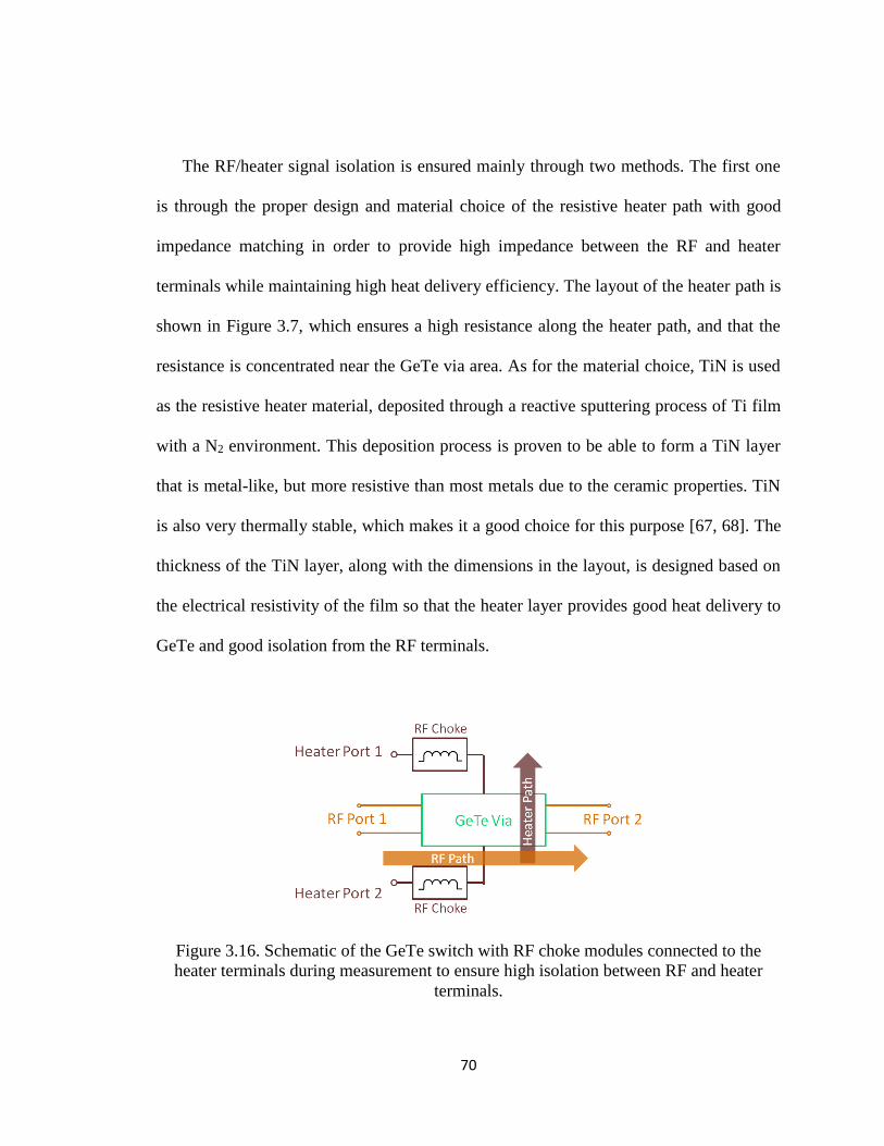
70
The RF/heater signal isolation is ensured mainly through two methods. The first one
is through the proper design and material choice of the resistive heater path with good
impedance matching in order to provide high impedance between the RF and heater
terminals while maintaining high heat delivery efficiency. The layout of the heater path is
shown in Figure 3.7, which ensures a high resistance along the heater path, and that the
resistance is concentrated near the GeTe via area. As for the material choice, TiN is used
as the resistive heater material, deposited through a reactive sputtering process of Ti film
with a N2 environment. This deposition process is proven to be able to form a TiN layer
that is metal-like, but more resistive than most metals due to the ceramic properties. TiN
is also very thermally stable, which makes it a good choice for this purpose [67, 68]. The
thickness of the TiN layer, along with the dimensions in the layout, is designed based on
the electrical resistivity of the film so that the heater layer provides good heat delivery to
GeTe and good isolation from the RF terminals.
Figure 3.16. Schematic of the GeTe switch with RF choke modules connected to the
heater terminals during measurement to ensure high isolation between RF and heater
terminals.

71
The other method to maintain high signal isolation between the RF and heater
terminals is through external circuit design. Compared to the operating frequency of the
switch for RF signal transmission, the heating current pulses are considered low
frequency. A good practice to improve isolation is to connect an RF choke to the heater
terminals in order to block the RF signal leakage. A simplified schematic configuration of
the device is shown in Figure 3.16.
Figure 3.17. The S21 response between an RF terminal and a heater terminal from
measurement and simulation with a 100 nH RF choke connected to the heater terminal.
To make sure that the RF power leakage through the heater terminals is not high
enough to cause operation issues, an RF transmission measurement between an RF
terminal and a heater terminal is performed to see the isolation. The results shown in
Figure 3.17 suggests that the isolation between the two terminals is above 20 dB, which is
considered high enough for low power operations, but with the RF choke modules
connected to the heater terminal during switching activities, an even higher isolation
between the RF and heater terminals can be achieved.

72
In order to evaluate the switching speed of the GeTe RF switches, measurement has
been taken with an oscilloscope where heating voltage pulses and RF signal are applied
to the GeTe switch and observed at the same time. In this measurement, the network
analyzer is connected to input RF port of the device as the RF signal source, and the
output RF port is connected to the oscilloscope for RF power level observation. The
heating path connection is the same as normal switch operation, where the heater
terminals are connected to the heating voltage source. Necessary matching networks are
connected to the terminals in order to isolate the RF and heating signals from each other.
A simplified block diagram for the measurement setup is shown in Figure 3.18.
Figure 3.18. Simplified block diagram showing the setup for switching speed
measurement for GeTe RF switches.
The heating voltage pulses are programmed and generated by the function generator
and amplified through an amplifier to obtain the desired amplitude. For GeTe

73
amorphization to turn the switch OFF, the heating pulse is set with a width of
approximately 0.5 s, and the rise and fall times are both 0.2 s. For GeTe crystallization
to turn the switch ON, the pulse rise time is still set at 0.2 s, but both the pulse width
and the fall time are extended to at least 1.5 s. The measurement results for switching
speed in both directions are shown in Figure 3.19. The switching speed is approximately
0.75 s for switching from ON to OFF, and 2.8 s from OFF to ON.
(a) (b)
Figure 3.19. Switching speed measurement of GeTe RF switch with direct heating
scheme (a) from ON to OFF and (b) from OFF to ON.
3.2.2. Four-Terminal GeTe RF Switch with Indirect Heating Scheme
While the direct heating method is a novel and efficient way of delivering phase
transition heat into the GeTe via of the RF switches, it has some limitations due to its
structure. Even though it has been verified that the electrical isolation between the RF
terminals and heater terminals can be maintained at a fairly high level, especially with the
external RF choke, the direct electrical contact among all four terminals demand the use
of a matching network, which adds to the overall size of the switch module. In order to
74
analyze and evaluate the advantage and disadvantage of the direct heating method, as
well as to have an alternative heating scheme, we have also designed and developed four-
terminal GeTe RF switches with the indirect heating method. In this type of GeTe RF
switches, the heater is not directly connected through the GeTe via, but instead embedded
underneath the main switch RF line and electrically isolated from the RF signal path. In
phase change RF switch community, this has been the more popular method and had
already been implemented and reported in several works with slightly different structures
[69] [70]. This sub-section will discuss the structure, principle of operation, fabrication
process, measurement and performance analysis of GeTe RF switches with indirect
heating scheme and provide a brief comparison between the two heating methods.
3.2.2.1. Device Structure
Similar to the phase change RF switches with direct heating scheme, the switch with
indirect heating one is also designed with two RF terminals laterally connected through a
GeTe via, forming the RF signal transmission path. But instead of running the Joule
heating current through the GeTe itself, a resistive heater is embedded underneath the
GeTe via, and the RF path and the heater path are electrically isolated (but thermally
coupled) with a dielectric layer.
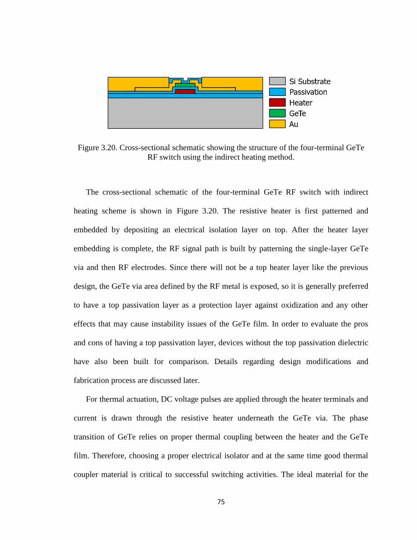
75
Figure 3.20. Cross-sectional schematic showing the structure of the four-terminal GeTe
RF switch using the indirect heating method.
The cross-sectional schematic of the four-terminal GeTe RF switch with indirect
heating scheme is shown in Figure 3.20. The resistive heater is first patterned and
embedded by depositing an electrical isolation layer on top. After the heater layer
embedding is complete, the RF signal path is built by patterning the single-layer GeTe
via and then RF electrodes. Since there will not be a top heater layer like the previous
design, the GeTe via area defined by the RF metal is exposed, so it is generally preferred
to have a top passivation layer as a protection layer against oxidization and any other
effects that may cause instability issues of the GeTe film. In order to evaluate the pros
and cons of having a top passivation layer, devices without the top passivation dielectric
have also been built for comparison. Details regarding design modifications and
fabrication process are discussed later.
For thermal actuation, DC voltage pulses are applied through the heater terminals and
current is drawn through the resistive heater underneath the GeTe via. The phase
transition of GeTe relies on proper thermal coupling between the heater and the GeTe
film. Therefore, choosing a proper electrical isolator and at the same time good thermal
coupler material is critical to successful switching activities. The ideal material for the
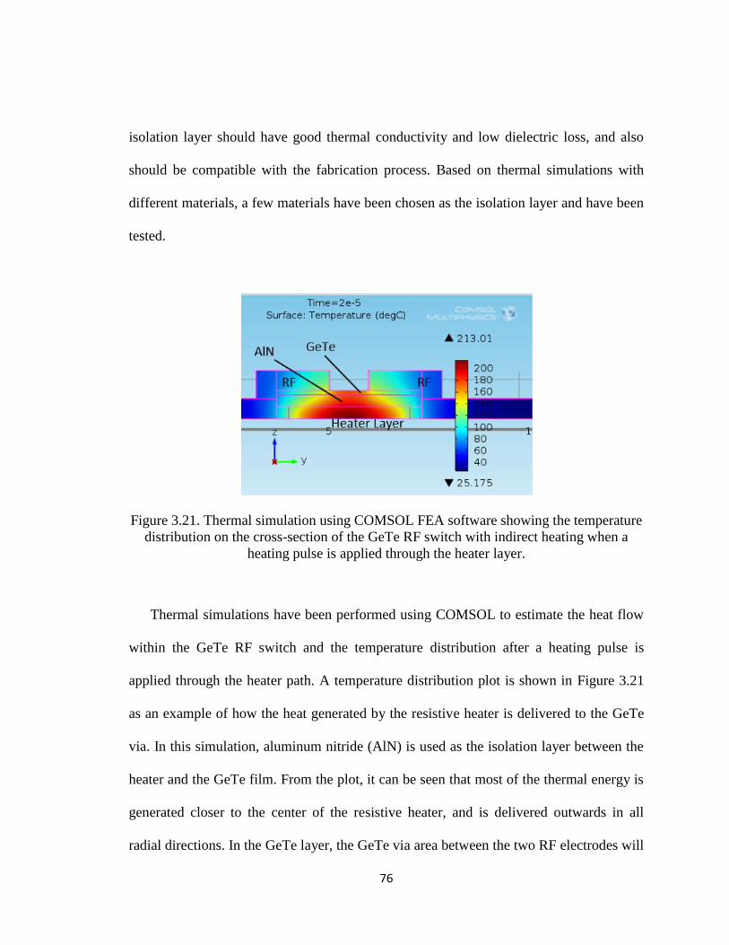
76
isolation layer should have good thermal conductivity and low dielectric loss, and also
should be compatible with the fabrication process. Based on thermal simulations with
different materials, a few materials have been chosen as the isolation layer and have been
tested.
Figure 3.21. Thermal simulation using COMSOL FEA software showing the temperature
distribution on the cross-section of the GeTe RF switch with indirect heating when a
heating pulse is applied through the heater layer.
Thermal simulations have been performed using COMSOL to estimate the heat flow
within the GeTe RF switch and the temperature distribution after a heating pulse is
applied through the heater path. A temperature distribution plot is shown in Figure 3.21
as an example of how the heat generated by the resistive heater is delivered to the GeTe
via. In this simulation, aluminum nitride (AlN) is used as the isolation layer between the
heater and the GeTe film. From the plot, it can be seen that most of the thermal energy is
generated closer to the center of the resistive heater, and is delivered outwards in all
radial directions. In the GeTe layer, the GeTe via area between the two RF electrodes will
77
be the first volume of GeTe to be heated up, and the GeTe areas that overlap with the RF
electrodes are heated up at a much slower rate. This heat distribution pattern has been
noticed during the simulation and has been taken advantage of in the design. During the
operation of the switch, the heating voltage pulses are controlled so that only the GeTe
via area is going through the phase transitions. The GeTe areas overlapping with the RF
electrodes will stay in the crystalline state at all times. This reduces the volume of GeTe
going through phase transitions, and will help obtain a faster switching speed.
3.2.2.2. Fabrication Process
GeTe RF switches with indirect heating scheme are also fabricated on passivated
silicon substrates. Since the indirect heating method needs to generate more thermal
power than the direct heating method due to the different thermal coupling mechanism, a
heat sink with a higher heat dissipation rate is preferred in order to maintain a high
heating/cooling speed and avoid potential device cross-talk. In order to satisfy the heat
dissipation speed requirements, the passivation layer needs to have a high thermal
conductivity as well as a decent heat capacity. For the same reason, different isolation
layer materials have also been tested. Details will be discussed in this sub-section.
The fabrication process of the GeTe RF switch with indirect heating has been
modified over time to ensure good layer quality and performance. The modifications
include both material choices and detailed fabrication parameters. A general process flow
of the devices is shown in Figure 3.22.

78
(a) Deposition of dielectric layer on substrate (b) Patterning of heater layer
(c) Deposition of isolation layer (d) Patterning of GeTe layer
(e) Patterning of RF electrodes layer (f) Deposition of top passivation and metals
Figure 3.22. Fabrication process flow of the GeTe RF switch with direct heating
The process starts with a dielectric layer deposition on the silicon substrate. This layer
is used as passivation to prevent DC current leakage into the substrate, and also as a heat
dissipation layer. The heater layer is patterned on top of the dielectric layer with a
thickness between 100 nm and 200 nm. While TiN is often used as the heater layer, other
materials including tungsten (W) and titanium-tungsten (TiW) have also been tested for
this purpose. The patterned resistive heater needs to be embedded before the deposition
of GeTe, and this is done by depositing another dielectric layer to ensure electrical
insulation between the heater layer and the GeTe layer. Since the terminal pads of the

79
heater layers need to be in contact with the RF probes for device measurements, the
dielectric layer is patterned through plasma etching to expose the pads of the heater layer.
The GeTe film is patterned with a thickness of approximately 100 nm. Other thicknesses
have also been used throughout the characterization as the thickness of GeTe film could
affect the crystallization process. After the patterning of GeTe film is complete, the RF
electrodes of gold with a thickness of 200 nm are patterned to establish contact with the
GeTe film as well as to define the via area. Finally, the gold metal routing and top
passivation layers are deposited and patterned.
During the GeTe deposition and patterning steps, it has been discovered that GeTe
films are often prone to possible damage from later processing steps, such as the
photoresist developer from the photolithography for the metal electrode contact layer, as
well as the solvents used for GeTe pattern lift-off. Since the film quality of GeTe plays a
vital role in the device performance, and it is important to ensure good GeTe-metal
contact, an additional protection layer covering the GeTe film has been deposited in
many fabricated sample. The deposition of the protection layer takes place immediately
after the sputtering of GeTe, and a thin film of molybdenum (Mo) is usually used. After
the metal electrode contact layer is patterned, the Mo protection layer on top of the GeTe
film will be shorting the electrodes because of the low electrical resistivity of Mo.
Therefore, an additional step to etch the exposed Mo layer is necessary to make sure that
the metal electrodes are connected only through the GeTe via. Etching for Mo is
performed using plasma SF6 etching, and the etching process needs to be well controlled
not to damage the GeTe layer underneath.
80
As discussed before, in GeTe RF switches with the direct heating scheme, the heater
material needs to have a high resistivity to ensure proper isolation between RF and DC
heating lines. In the indirect heating design, since the heater in not in direct contact with
the GeTe via, other choices of heater materials can be considered. Since the localized
peak temperature from the heater could be as high as 800°C, the heater material is
required to be stable at high temperatures. While TiN has been proven to have high
temperature durability, its high electrical resistivity results in high power consumption.
Tungsten (W) has been tested as an alternative heater material since it has a much lower
resistivity and decent high temperature stability. Other suitable materials tested include
an alloy of titanium and tungsten (TiW). The reliability of the heater layer is very critical
to the reliability of the switch. Therefore, further investigation into the heater robustness
has been performed regarding both material choice and fabrication process that will be
discussed later.
As previously mentioned, the bottom dielectric layer for substrate passivation and the
isolation layer between the heater and GeTe also serve as heat conduction layers. In order
to ensure fast and effective switching, the dielectric materials are preferred to have good
thermal properties such has high thermal conductivity. Among the common choices of
dielectric layers, aluminum nitride (AlN) has much higher thermal conductivity than
silicon dioxide or silicon nitride [71], and is a good choice for both the bottom
passivation layer and the isolation layer.
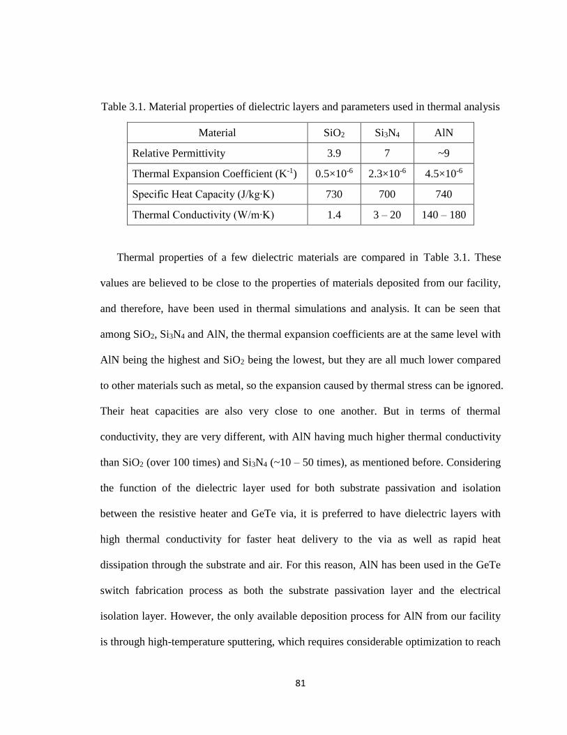
81
Table 3.1. Material properties of dielectric layers and parameters used in thermal analysis
Material SiO2 Si3N4 AlN
Relative Permittivity 3.9 7 ~9
Thermal Expansion Coefficient (K-1) 0.5×10⁻⁶ 2.3×10⁻⁶ 4.5×10⁻⁶
Specific Heat Capacity (J/kg∙K) 730 700 740
Thermal Conductivity (W/m∙K) 1.4 3 – 20 140 – 180
Thermal properties of a few dielectric materials are compared in Table 3.1. These
values are believed to be close to the properties of materials deposited from our facility,
and therefore, have been used in thermal simulations and analysis. It can be seen that
among SiO2, Si3N4 and AlN, the thermal expansion coefficients are at the same level with
AlN being the highest and SiO2 being the lowest, but they are all much lower compared
to other materials such as metal, so the expansion caused by thermal stress can be ignored.
Their heat capacities are also very close to one another. But in terms of thermal
conductivity, they are very different, with AlN having much higher thermal conductivity
than SiO2 (over 100 times) and Si3N4 (~10 – 50 times), as mentioned before. Considering
the function of the dielectric layer used for both substrate passivation and isolation
between the resistive heater and GeTe via, it is preferred to have dielectric layers with
high thermal conductivity for faster heat delivery to the via as well as rapid heat
dissipation through the substrate and air. For this reason, AlN has been used in the GeTe
switch fabrication process as both the substrate passivation layer and the electrical
isolation layer. However, the only available deposition process for AlN from our facility
is through high-temperature sputtering, which requires considerable optimization to reach
82
high-quality films. On the other hand, SiO2 layers can be thermally grown using a mature
process on silicon substrates, yielding very good film quality. And since compared to the
silicon substrate, the passivation layer is much thinner, SiO2 has also been considered as
the passivation layer choice in some fabricated batches.
As for the isolation layer between the resistive heater and the GeTe film, while high
thermal conductivity is preferred for fast heat delivery, another important factor to
consider is the quality of the GeTe film deposited on the isolation layer. Experimental
results show that the GeTe film deposited on top of an aluminum nitride layer tends to
have degraded quality in terms of both adhesion and crystallinity after annealing. The
reason may be low sputtered AlN quality in test samples or different crystalline structure
of AlN and GeTe, making AlN a poor choice of seedlayer for GeTe. As an alternative,
silicon nitride has been tested as the isolation layer, and GeTe films deposited on top of
silicon nitride tend to have a better adhesion as well as better crystallization results. Even
though the relatively low thermal conductivity of silicon nitride reduces the heating
efficiency, but with a reduction in the layer’s thickness as well as other fabrication detail
modifications, the trade-off can be managed.
During the fabrication process, GeTe film quality issues aroused quite often. The
most common issues include bad adhesion with GeTe peeling off after lift-off process,
stress induced surface defects and cracking, and poor crystallization. Since the quality of
GeTe films is critical to the functionality and performance of the switches, an alternative
approach for GeTe layer patterning was developed. Instead of using lift-off as the
patterning method, the GeTe film is patterned with plasma etching. According to the test
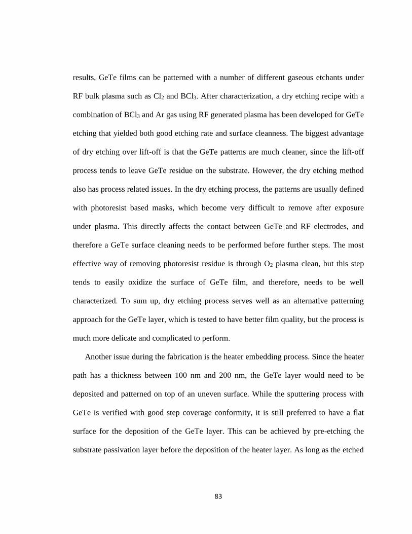
83
results, GeTe films can be patterned with a number of different gaseous etchants under
RF bulk plasma such as Cl2 and BCl3. After characterization, a dry etching recipe with a
combination of BCl3 and Ar gas using RF generated plasma has been developed for GeTe
etching that yielded both good etching rate and surface cleanness. The biggest advantage
of dry etching over lift-off is that the GeTe patterns are much cleaner, since the lift-off
process tends to leave GeTe residue on the substrate. However, the dry etching method
also has process related issues. In the dry etching process, the patterns are usually defined
with photoresist based masks, which become very difficult to remove after exposure
under plasma. This directly affects the contact between GeTe and RF electrodes, and
therefore a GeTe surface cleaning needs to be performed before further steps. The most
effective way of removing photoresist residue is through O2 plasma clean, but this step
tends to easily oxidize the surface of GeTe film, and therefore, needs to be well
characterized. To sum up, dry etching process serves well as an alternative patterning
approach for the GeTe layer, which is tested to have better film quality, but the process is
much more delicate and complicated to perform.
Another issue during the fabrication is the heater embedding process. Since the heater
path has a thickness between 100 nm and 200 nm, the GeTe layer would need to be
deposited and patterned on top of an uneven surface. While the sputtering process with
GeTe is verified with good step coverage conformity, it is still preferred to have a flat
surface for the deposition of the GeTe layer. This can be achieved by pre-etching the
substrate passivation layer before the deposition of the heater layer. As long as the etched

84
thickness of the passivation layer is controlled to be the same as the heater layer, a flat
surface can be achieved.
A schematic showing the difference between the substrate stack with and without the
pre-etching process prior to the heater layer pattering is shown in Figure 3.23. With a
well-controlled pre-etching process, the surface after deposition of isolation layer can be
made flat for the GeTe layer deposition. In reality, however, the lift-off process of heater
layers also tends to leave patterns with sharp edges, and the height of the wall-shaped
edges is often several times more than the intended thickness of the layer. With this
problem, even a pre-etching process of the passivation layer cannot ensure a good flat
surface, and an additional polishing step is needed to address this issue. In this work, a
meticulous heater embedding process flow has been developed and is shown in Figure
3.24. This procedure is performed after the deposition of the dielectric passivation layer
on the silicon substrate. Before depositing the heater layer, a plasma etching is performed
on the passivation layer. The heater layer is deposited and patterned using the same mask
as the previous step, followed by a mechanical polishing process to remove any residue
on the edges of the patterns. Then a dielectric layer is deposited on top as the isolation
between the heater and GeTe. It is difficult to keep the surface perfectly flat at this point,
because the pre-etching depth and the heater deposition thickness cannot be exactly
matched. Therefore, a chemical-mechanical planarization (CMP) is used to polish the
isolation layer. Since polishing could greatly reduce the thickness of the dielectric, an
additional deposition is preferred afterwards. This heater embedding process can help
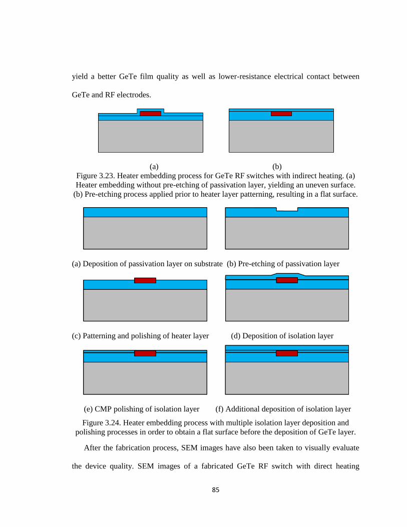
85
yield a better GeTe film quality as well as lower-resistance electrical contact between
GeTe and RF electrodes.
(a) (b)
Figure 3.23. Heater embedding process for GeTe RF switches with indirect heating. (a)
Heater embedding without pre-etching of passivation layer, yielding an uneven surface.
(b) Pre-etching process applied prior to heater layer patterning, resulting in a flat surface.
(a) Deposition of passivation layer on substrate (b) Pre-etching of passivation layer
(c) Patterning and polishing of heater layer (d) Deposition of isolation layer
(e) CMP polishing of isolation layer (f) Additional deposition of isolation layer
Figure 3.24. Heater embedding process with multiple isolation layer deposition and
polishing processes in order to obtain a flat surface before the deposition of GeTe layer.
After the fabrication process, SEM images have also been taken to visually evaluate
the device quality. SEM images of a fabricated GeTe RF switch with direct heating
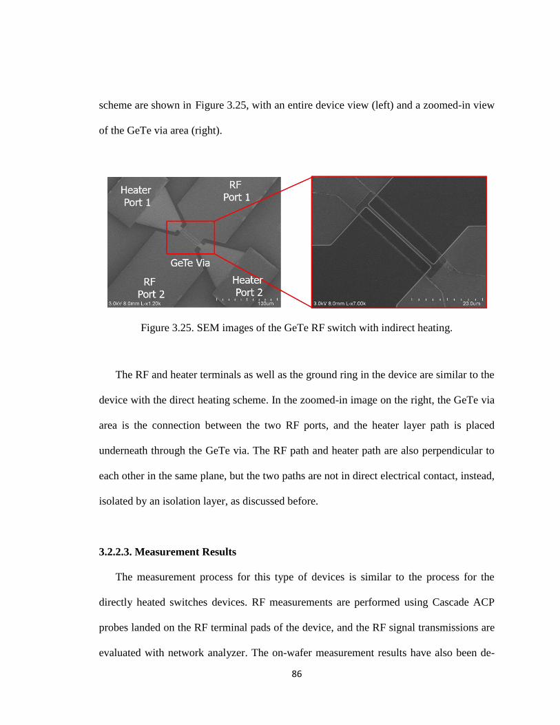
86
scheme are shown in Figure 3.25, with an entire device view (left) and a zoomed-in view
of the GeTe via area (right).
Figure 3.25. SEM images of the GeTe RF switch with indirect heating.
The RF and heater terminals as well as the ground ring in the device are similar to the
device with the direct heating scheme. In the zoomed-in image on the right, the GeTe via
area is the connection between the two RF ports, and the heater layer path is placed
underneath through the GeTe via. The RF path and heater path are also perpendicular to
each other in the same plane, but the two paths are not in direct electrical contact, instead,
isolated by an isolation layer, as discussed before.
3.2.2.3. Measurement Results
The measurement process for this type of devices is similar to the process for the
directly heated switches devices. RF measurements are performed using Cascade ACP
probes landed on the RF terminal pads of the device, and the RF signal transmissions are
evaluated with network analyzer. The on-wafer measurement results have also been de-
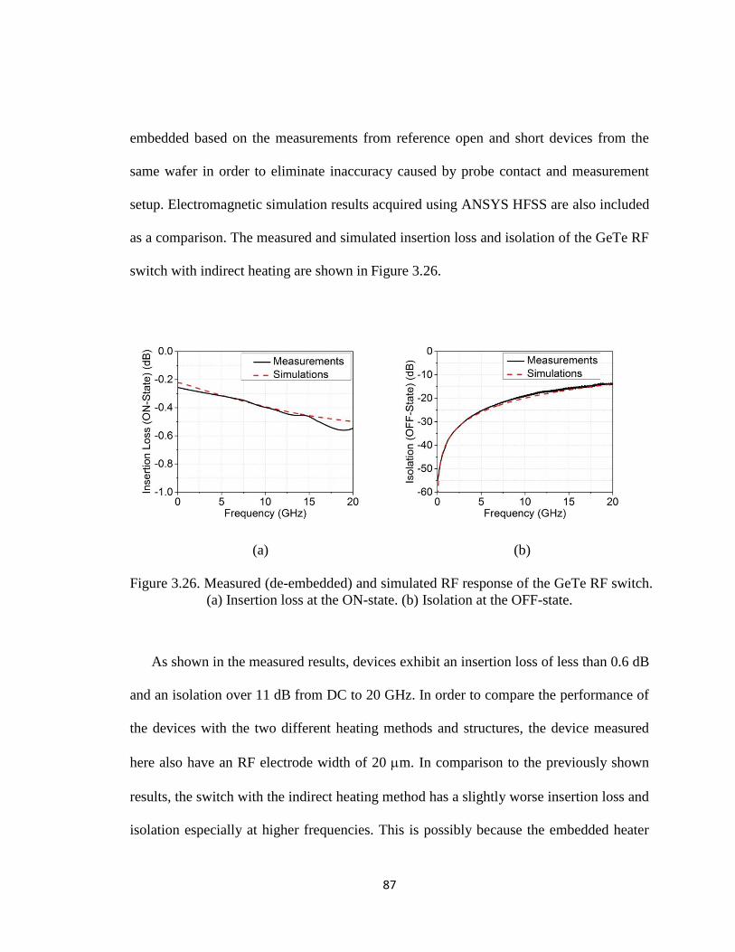
87
embedded based on the measurements from reference open and short devices from the
same wafer in order to eliminate inaccuracy caused by probe contact and measurement
setup. Electromagnetic simulation results acquired using ANSYS HFSS are also included
as a comparison. The measured and simulated insertion loss and isolation of the GeTe RF
switch with indirect heating are shown in Figure 3.26.
(a) (b)
Figure 3.26. Measured (de-embedded) and simulated RF response of the GeTe RF switch.
(a) Insertion loss at the ON-state. (b) Isolation at the OFF-state.
As shown in the measured results, devices exhibit an insertion loss of less than 0.6 dB
and an isolation over 11 dB from DC to 20 GHz. In order to compare the performance of
the devices with the two different heating methods and structures, the device measured
here also have an RF electrode width of 20 m. In comparison to the previously shown
results, the switch with the indirect heating method has a slightly worse insertion loss and
isolation especially at higher frequencies. This is possibly because the embedded heater
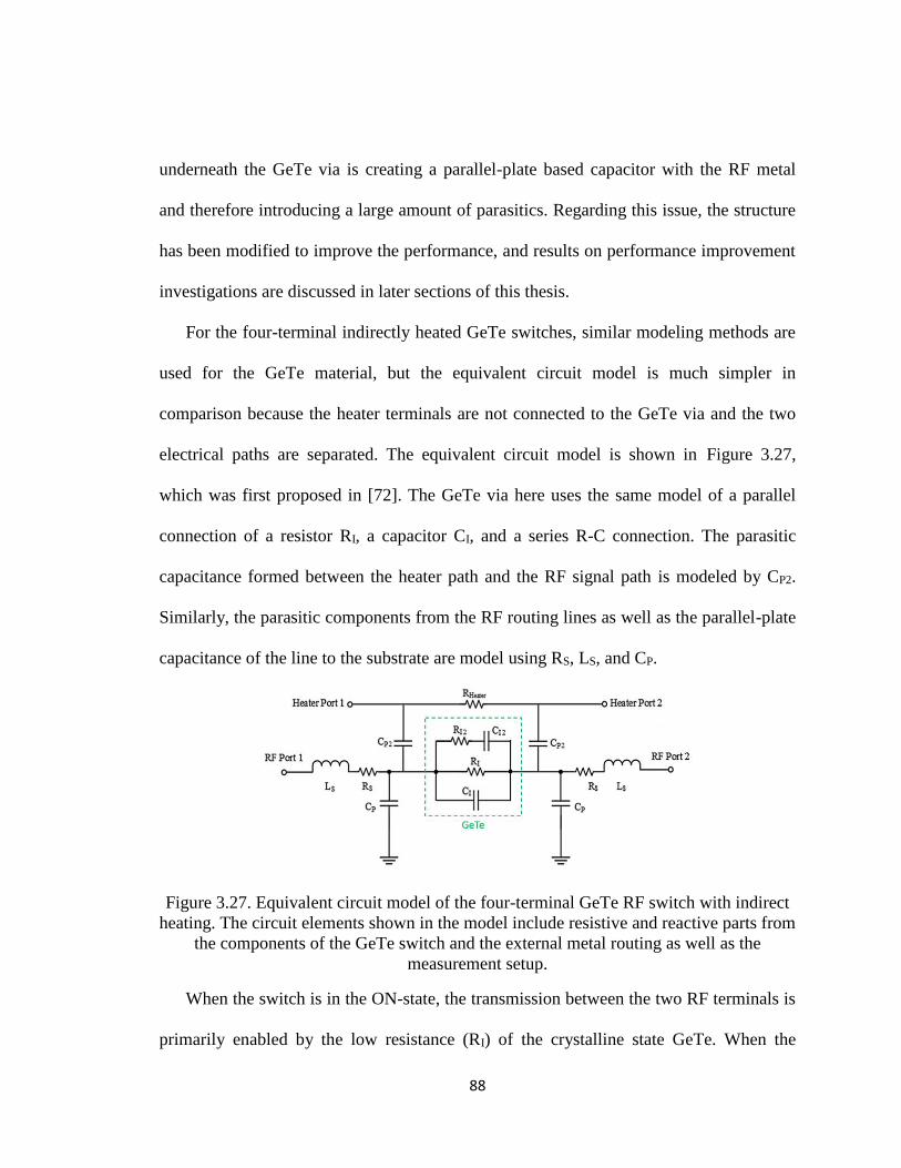
88
underneath the GeTe via is creating a parallel-plate based capacitor with the RF metal
and therefore introducing a large amount of parasitics. Regarding this issue, the structure
has been modified to improve the performance, and results on performance improvement
investigations are discussed in later sections of this thesis.
For the four-terminal indirectly heated GeTe switches, similar modeling methods are
used for the GeTe material, but the equivalent circuit model is much simpler in
comparison because the heater terminals are not connected to the GeTe via and the two
electrical paths are separated. The equivalent circuit model is shown in Figure 3.27,
which was first proposed in [72]. The GeTe via here uses the same model of a parallel
connection of a resistor RI, a capacitor CI, and a series R-C connection. The parasitic
capacitance formed between the heater path and the RF signal path is modeled by CP2.
Similarly, the parasitic components from the RF routing lines as well as the parallel-plate
capacitance of the line to the substrate are model using RS, LS, and CP.
Figure 3.27. Equivalent circuit model of the four-terminal GeTe RF switch with indirect
heating. The circuit elements shown in the model include resistive and reactive parts from
the components of the GeTe switch and the external metal routing as well as the
measurement setup.
When the switch is in the ON-state, the transmission between the two RF terminals is
primarily enabled by the low resistance (RI) of the crystalline state GeTe. When the

89
switch is in the OFF-state, the resistance between the RF terminals becomes much higher,
and the capacitance becomes the dominant factor in determining the RF isolation. When
the switch is turned ON, the resistance from the RF terminals is 𝑅𝑂𝑁 ≈ 3 Ω, and when it
is turned OFF, the capacitance from the RF terminals is 𝐶𝑂𝐹𝐹 ≈ 12.5 fF. Therefore, the
switch is measured to have a cut-off frequency of 4.2 THz.
The key to improving the performance of the indirectly heated GeTe RF switch is to
reduce the parasitic capacitance, which can be done by optimizing the structure and
sizing of the GeTe via and the resistive heater. In the device measured above, the
resistive heater path has a width of approximately 7 m, which is decided according to
the thermal simulation results. As discussed before, the resistive heater and the RF signal
path form a parallel-plate based capacitor, which greatly increases the parasitics of the
device. If the width of the heater path is reduced, the heater resistance is increased, which
results in higher heating voltage for thermal actuation. On the other hand, the parasitic
capacitance can be reduced so that the RF performance of the switch is improved. In
order to explore this trade-off, devices with a heater width of 3 m have been fabricated
and tested. According to the test results, the required voltage of the heating pulses is 30%
to 50% higher than the previous design, but the RF performance has shown great
improvement, with the device having an insertion loss that is lower by ~0.3 dB.
With the width of the resistive heater path reduced, another significant change is the
more localized heating on the GeTe film. The volume of GeTe film that is experiencing
phase transitions is only limited to the via connecting the RF electrodes, rather than the
entire GeTe pad as in the previous design.

90
Figure 3.28. TEM images showing the GeTe RF switch (a) when in the OFF state, (b) the
enhanced view of the GeTe film where only the GeTe volume at the via area is
amorphous, and most GeTe volume remains crystalline. (c) High-resolution TEM image
showing the crystalline-amorphous interface of the GeTe film.
As shown in Figure 3.28, with the width of the resistive heater path reduced in the
modified design, when the GeTe switch is turned OFF, only the GeTe area between the
RF electrodes is in amorphous phase, while the rest of the GeTe film stays in crystalline
state at all times. Since the total volume of GeTe going through phase transitions during
switching activities is reduced, the switching speed of the switch is improved. More
importantly, since the amorphous state GeTe behaves like dielectric material with a high
dielectric constant, this modified design reduces the parasitic capacitance formed
between the RF electrodes and resistive heater path compared to the previous design.
This is another significant contribution to the high-frequency performance of the GeTe
switch.
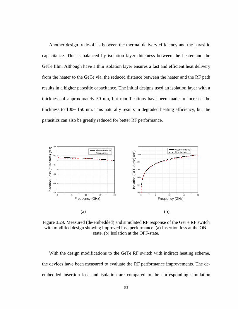
91
Another design trade-off is between the thermal delivery efficiency and the parasitic
capacitance. This is balanced by isolation layer thickness between the heater and the
GeTe film. Although have a thin isolation layer ensures a fast and efficient heat delivery
from the heater to the GeTe via, the reduced distance between the heater and the RF path
results in a higher parasitic capacitance. The initial designs used an isolation layer with a
thickness of approximately 50 nm, but modifications have been made to increase the
thickness to 100~ 150 nm. This naturally results in degraded heating efficiency, but the
parasitics can also be greatly reduced for better RF performance.
(a) (b)
Figure 3.29. Measured (de-embedded) and simulated RF response of the GeTe RF switch
with modified design showing improved loss performance. (a) Insertion loss at the ON-
state. (b) Isolation at the OFF-state.
With the design modifications to the GeTe RF switch with indirect heating scheme,
the devices have been measured to evaluate the RF performance improvements. The de-
embedded insertion loss and isolation are compared to the corresponding simulation
0 5 10 15 20
-1.0
-0.8
-0.6
-0.4
-0.2
0.0
Inse
rtio
n L
oss (
ON
-Sta
te)
(dB
)
Frequency (GHz)
Measurements
Simulations
0 5 10 15 20
-60
-50
-40
-30
-20
-10
0
Isola
tion (
OF
F-S
tate
) (d
B)
Frequency (GHz)
Measurements
Simulations

92
results (Figure 3.29). The ON-state insertion loss has been reduced to approximately 0.3
dB at 20 GHz. Other than the modifications discussed above, a more aggressive sizing
has also helped reduce the insertion loss. The OFF-state isolation of the device is still
above 11 dB from DC to 20 GHz. Even though the parasitics have been reduced, the
isolation was traded off with the insertion loss. The figure-of-merit cut-off frequency for
this improved design is approximately 5.6 THz, which is a performance improvement
compared to the previous design.
The switching speed of the GeTe RF switch with indirect heating scheme is also
evaluated using the same setup. Since the phase transition process is a property of the
GeTe film, the switching speed of the switch with indirect heating is similar to that with
direct heating. The difference in switching speed is due to the structural difference, which
results in difference in heat delivery and dissipation rate. Figure 3.30 shows the measured
switching speed for the device. The switching time is around 0.6 s to turn the switch
OFF and 2 s to turn the switch ON.
(a) (b)
Figure 3.30. Switching speed measurement of GeTe RF switch with indirect heating
scheme (a) from ON to OFF and (b) from OFF to ON.

93
Table 3.2. Comparison of performance among different GeTe RF switch designs
Design Insertion
Loss Isolation RON ROFF ROFF/RON COFF 𝑓𝑐𝑜
Heating
Power
Direct
Heating
0.5 dB
@
20 GHz
18 dB 5 Ω 18 kΩ 4×10³ 8 fF 4 THz 85 mW/
cycle
Indirect
Heating
0.6 dB
@
20 GHz
11 dB 3 Ω 20 kΩ 5×10³ 12.5 fF 4.2 THz 300 mW/
cycle
Indirect
Heating
(Modified)
0.3 dB
@
20 GHz
11 dB 2.7 Ω 22 kΩ 8×10³ 10.5 fF 5.6 THz 500 mW/
cycle
In order to better compare the RF performance among the different types of switches,
some of the RF measurement data are shown in Table 3.2. With similar dimensions, the
first two designs of switches show similar RF responses, and the differences mainly result
from the structure induced parasitics, which are different for the two switch types. The
modified GeTe switch with indirect heating scheme uses more aggressive sizing for
improved RF performance, but the heating power is increased as a trade-off. In terms of
integration compatibility and ease of fabrication, the indirectly heated switch design is
advantageous.
3.3. Power Handling Analysis and Thermoelectric Modeling
Due to the fact that the GeTe phase change switches rely on thermal actuation to
achieve switching, the transmitted RF signals could interfere with the phase transitions of
GeTe if the RF power level gets sufficiently high, and the switch linearity and power
handling capability could therefore be affected. This kind of self-actuation needs to be

94
avoided. In order to better analyze the thermal properties of the GeTe switches, a
modeling method linking the thermal and electrical properties of the GeTe via and the
switch was proposed. This method can be used to model the switch operation at different
RF power levels, and explore how high RF power interferes with the stability of the GeTe
film and the linearity of the RF response. The earliest reported effect to model the non-
linearity response of the GeTe based RF switch can be found in [73], which relates the
physical properties of GeTe such as the electrical resistivity and thermal conductivity to
the heating effect from the RF signals. An improved modeling method based on this was
later proposed with more accurate results on predicting the input third-order intercept
point (IIP3) and 1-dB compression point (P1dB) for the switch [72]. This new method, the
thermoelectric modeling method, relates the thermal activity caused by the RF signals
through the switch to the property change of the GeTe film. The diagram for the
thermoelectric model is shown in Figure 3.31.
Figure 3.31. The thermoelectric model of the GeTe based RF switches. This model
consists of a simplified equivalent circuit model of the phase change switch, and the heat
transfer function as well as the modeling of the changing electrical resistivity of GeTe
with changing temperature and voltage across the phase change layer.

95
In this model, the equivalent circuit for the GeTe switch is simplified to a parallel
connection of a resistor with a changing resistance and a capacitor, with different element
values for each type of the switch. The heat transfer function is modeled based on
Equation (3.1). The electrical resistivity of the GeTe at the crystalline and amorphous
states are modeled based on Equations (3.2) and (3.3), where k, q, τ0, EF, V, Δz and ua
indicate the Boltzmann constant, elementary charge, time constant for trapped electrons,
Fermi level, applied voltage, short trap distance, and effective thickness of the GeTe layer,
respectively.
𝐻(𝜔) =Δ𝑇
𝑃=
1
𝑉𝑚⋅
𝑑𝑚[(𝑑𝑓 𝑘𝑓⁄ )⋅(tanh𝛽𝑓 𝛽𝑓⁄ )+𝑅𝐵]
1+𝑗𝜔𝐶𝑚𝑑𝑚[(𝑑𝑓 𝑘𝑓)⋅(tanh𝛽𝑓 𝛽𝑓⁄ +𝑅𝐵)⁄ ], 𝛽𝑓 = 𝑑_𝑓√𝑗2𝜋𝑓ℎ
𝐶𝑓
𝑘𝑓∙(3.1)
𝜌𝑐𝑟𝑦𝑠𝑡𝑎𝑙𝑙𝑖𝑛𝑒 = 𝜌0[1 + 𝛼(𝑇 − 𝑇𝑟𝑒𝑓)] ∙∙∙∙∙∙∙∙∙∙∙∙∙∙∙∙∙∙∙∙∙∙∙∙∙∙∙∙∙∙∙∙∙∙∙∙∙∙∙∙∙∙∙∙∙∙∙∙∙∙∙∙∙∙∙∙∙∙∙∙∙∙∙∙∙∙∙∙∙∙(3.2)
𝜌𝑎𝑚𝑜𝑟𝑝ℎ𝑜𝑢𝑠 =𝑘𝑇𝜏0
(𝑞Δ𝑧)2𝑁𝑇𝑒−
(𝐸𝐶−𝐸𝐹)
𝑘𝑇 cosh−1(𝑞𝑉𝐴
𝑘𝑇
Δ𝑧
2𝑢𝑎) ∙∙∙∙∙∙∙∙∙∙∙∙∙∙∙∙∙∙∙∙∙∙∙∙∙∙∙∙∙∙∙∙∙∙∙∙∙∙∙∙∙∙∙∙(3.3)
The temperature rise (∆T) of the GeTe layer from the heating power (P) can be
estimated using the heat transfer function (Equation (3.1)) [74]. At the crystalline state,
the resistivity exhibits metal-like temperature dependence (Equation (3.2)) [55]. We
measured the TCR (α) of GeTe to be 2.3×10⁻³/K in this state, which is close to the value
reported in [55]. The Poole-Frenkel (PF) model is used in the amorphous state to model
the change of the resistivity of GeTe (Equation (3.3)) [47]. The two main parameters in
Equation (3.3) are EC-EF (energy distance between the Fermi level and the conduction
96
band) and NT (trap concentration). Reducing EC-EF and increasing NT make the
amorphous resistivity vary less with temperature rise and high voltage swings,
respectively, which results in improved P1dB and IIP3.
The simulated frequency of the heat transfer function based on Equation (3.1) show a
low-pass characteristic for both types of switches [74]. The low frequency transfer
function gain is much dependent on the dimensions of the GeTe patch connecting the RF
pads and the thermal properties of the material surrounding the GeTe [72]. The two
switch types that were measured have similar thermal transfer functions since they have
similar dimensions of the GeTe pad, and similar thermal properties of the two structures,
except that the directly heated switch has both a top and bottom heater layer in contact
with GeTe, whereas the indirectly heated switch only has a bottom isolation layer
underneath with a smaller thickness. Therefore, the directly heated switch has a better
heat capacitance compared to the indirectly heated one, resulting in a slightly better
linearity.
The measured response of the switch and predicted response using the thermoelectric
model are compared in Figure 3.32. As can be seen, the input third-order intercept points
(IIP3s) are both measured to be around 30 dBm, which vary at different center
frequencies and different frequency offsets. For both types of switches, the IIP3 response
at the ON state shows an increasing trend as the frequency offset increases. This is
because with a higher frequency offset, the mixed term in the IIP3 measurement is
suppressed, so the third-order inter-modulation signal is lower, and thus the linearity is
better. The changing center frequency, however, barely affects the linearity since the
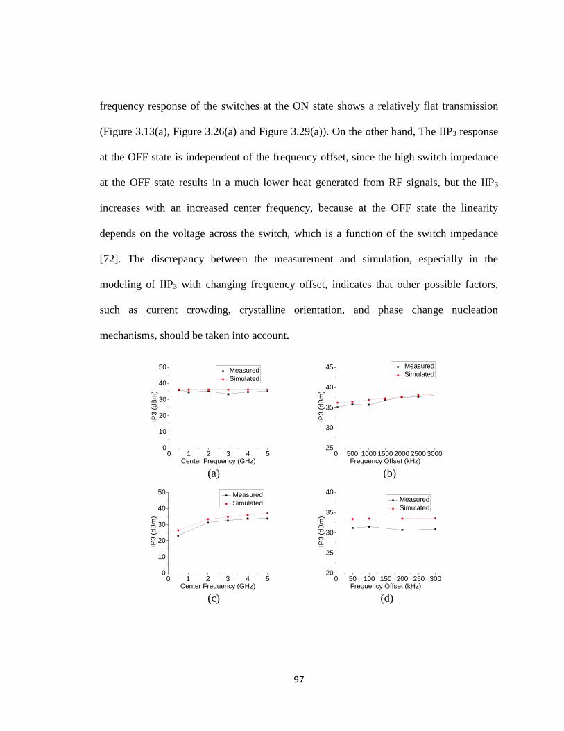
97
frequency response of the switches at the ON state shows a relatively flat transmission
(Figure 3.13(a), Figure 3.26(a) and Figure 3.29(a)). On the other hand, The IIP3 response
at the OFF state is independent of the frequency offset, since the high switch impedance
at the OFF state results in a much lower heat generated from RF signals, but the IIP3
increases with an increased center frequency, because at the OFF state the linearity
depends on the voltage across the switch, which is a function of the switch impedance
[72]. The discrepancy between the measurement and simulation, especially in the
modeling of IIP3 with changing frequency offset, indicates that other possible factors,
such as current crowding, crystalline orientation, and phase change nucleation
mechanisms, should be taken into account.
(a) (b)
(c) (d)
0 1 2 3 4 50
10
20
30
40
50
IIP
3 (
dB
m)
Center Frequency (GHz)
Measured
Simulated
0 500 1000 1500 2000 2500 300025
30
35
40
45
IIP
3 (
dB
m)
Frequency Offset (kHz)
Measured
Simulated
0 1 2 3 4 50
10
20
30
40
50
IIP
3 (
dB
m)
Center Frequency (GHz)
Measured
Simulated
0 50 100 150 200 250 30020
25
30
35
40
IIP
3 (
dB
m)
Frequency Offset (kHz)
Measured
Simulated
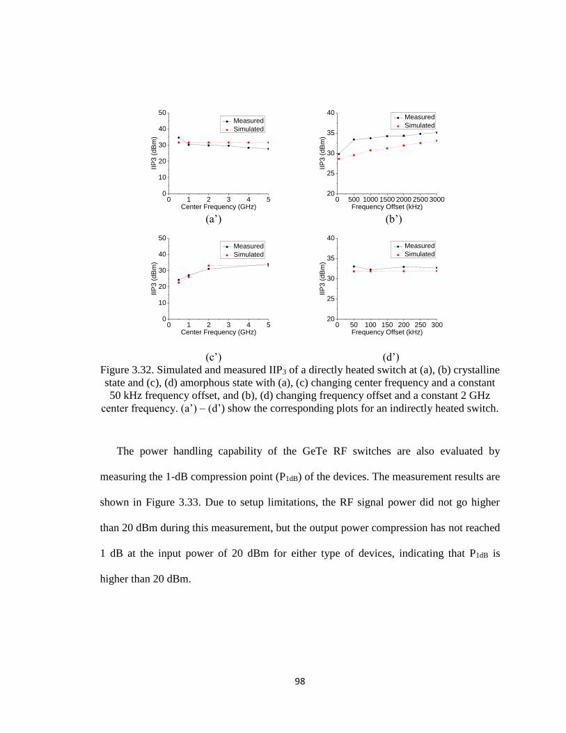
98
(a’) (b’)
(c’) (d’)
Figure 3.32. Simulated and measured IIP3 of a directly heated switch at (a), (b) crystalline
state and (c), (d) amorphous state with (a), (c) changing center frequency and a constant
50 kHz frequency offset, and (b), (d) changing frequency offset and a constant 2 GHz
center frequency. (a’) – (d’) show the corresponding plots for an indirectly heated switch.
The power handling capability of the GeTe RF switches are also evaluated by
measuring the 1-dB compression point (P1dB) of the devices. The measurement results are
shown in Figure 3.33. Due to setup limitations, the RF signal power did not go higher
than 20 dBm during this measurement, but the output power compression has not reached
1 dB at the input power of 20 dBm for either type of devices, indicating that P1dB is
higher than 20 dBm.
0 1 2 3 4 50
10
20
30
40
50
IIP
3 (
dB
m)
Center Frequency (GHz)
Measured
Simulated
0 500 1000 1500 2000 2500 300020
25
30
35
40
IIP
3 (
dB
m)
Frequency Offset (kHz)
Measured
Simulated
0 1 2 3 4 50
10
20
30
40
50
IIP
3 (
dB
m)
Center Frequency (GHz)
Measured
Simulated
0 50 100 150 200 250 30020
25
30
35
40
IIP
3 (
dB
m)
Frequency Offset (kHz)
Measured
Simulated
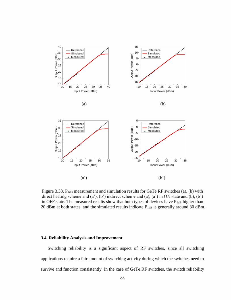
99
(a) (b)
(a’) (b’)
Figure 3.33. P1dB measurement and simulation results for GeTe RF switches (a), (b) with
direct heating scheme and (a’), (b’) indirect scheme and (a), (a’) in ON state and (b), (b’)
in OFF state. The measured results show that both types of devices have P1dB higher than
20 dBm at both states, and the simulated results indicate P1dB is generally around 30 dBm.
3.4. Reliability Analysis and Improvement
Switching reliability is a significant aspect of RF switches, since all switching
applications require a fair amount of switching activity during which the switches need to
survive and function consistently. In the case of GeTe RF switches, the switch reliability
10 15 20 25 30 35 4010
15
20
25
30
35
40
Outp
ut P
ow
er
(dB
m)
Input Power (dBm)
Reference
Simulated
Measured
10 15 20 25 30 35 40
-15
-10
-5
0
5
10
15
Outp
ut P
ow
er
(dB
m)
Input Power (dBm)
Reference
Simulated
Measured
10 15 20 25 30 3510
15
20
25
30
35
Outp
ut P
ow
er
(dB
m)
Input Power (dBm)
Reference
Simulated
Measured
10 15 20 25 30 35-25
-20
-15
-10
-5
0
5
Outp
ut P
ow
er
(dB
m)
Input Power (dBm)
Reference
Simulated
Measured
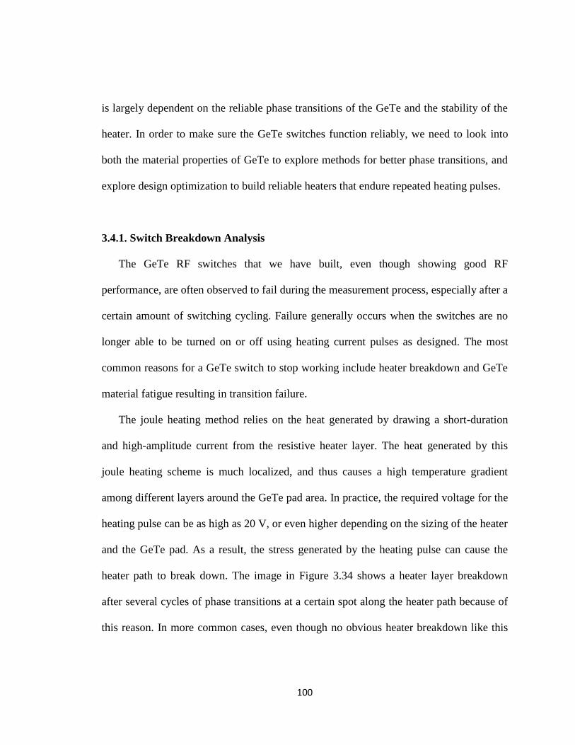
100
is largely dependent on the reliable phase transitions of the GeTe and the stability of the
heater. In order to make sure the GeTe switches function reliably, we need to look into
both the material properties of GeTe to explore methods for better phase transitions, and
explore design optimization to build reliable heaters that endure repeated heating pulses.
3.4.1. Switch Breakdown Analysis
The GeTe RF switches that we have built, even though showing good RF
performance, are often observed to fail during the measurement process, especially after a
certain amount of switching cycling. Failure generally occurs when the switches are no
longer able to be turned on or off using heating current pulses as designed. The most
common reasons for a GeTe switch to stop working include heater breakdown and GeTe
material fatigue resulting in transition failure.
The joule heating method relies on the heat generated by drawing a short-duration
and high-amplitude current from the resistive heater layer. The heat generated by this
joule heating scheme is much localized, and thus causes a high temperature gradient
among different layers around the GeTe pad area. In practice, the required voltage for the
heating pulse can be as high as 20 V, or even higher depending on the sizing of the heater
and the GeTe pad. As a result, the stress generated by the heating pulse can cause the
heater path to break down. The image in Figure 3.34 shows a heater layer breakdown
after several cycles of phase transitions at a certain spot along the heater path because of
this reason. In more common cases, even though no obvious heater breakdown like this

101
takes place, the stress generated by the heating pulses could result in gradual increase of
the heater resistance, which eventually causes the heater to fail.
Figure 3.34. SEM images of a GeTe phase change switch with a breaking point along the
heater path. This breakdown is cause by the high stress generated due to the high voltage
of the heating pulses during phase transitions.
Among reported works on GeTe based phase change switches, the thin-film resistive
materials that have been used for heater include SiCr, NiSiCr, TiN as well as a few types
of metals such as Ti or W. The bottom passivation layer underneath the heater path is
most typically SiN, AlN, or SiO2, and the passivation layer on top of the heater path that
serves as the isolation/thermal coupling layer is usually Si3N4. Based on the thermal and
dielectric properties of these materials, a simulation recreating the heat distribution
condition during phase transition is performed to analyze how much stress is generated.
The simulated result of the heater in the SiO2-W-Si3N4 configuration is shown in Figure
3.35(a). As comparison, a layer configuration with aluminum nitride (AlN) as the
substitute material for SiO2 and Si3N4 for both the passivation layer and isolation layer is
simulated and included in Figure 3.35(b), considering the good thermal conductivity of
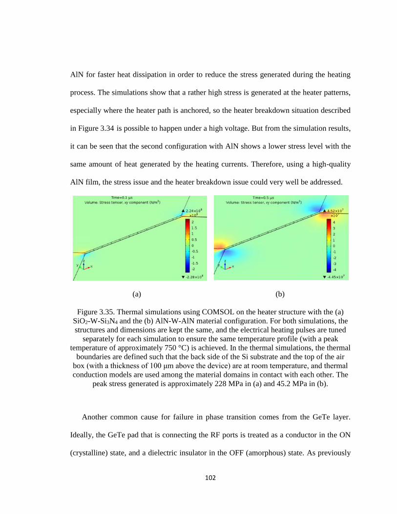
102
AlN for faster heat dissipation in order to reduce the stress generated during the heating
process. The simulations show that a rather high stress is generated at the heater patterns,
especially where the heater path is anchored, so the heater breakdown situation described
in Figure 3.34 is possible to happen under a high voltage. But from the simulation results,
it can be seen that the second configuration with AlN shows a lower stress level with the
same amount of heat generated by the heating currents. Therefore, using a high-quality
AlN film, the stress issue and the heater breakdown issue could very well be addressed.
(a) (b)
Figure 3.35. Thermal simulations using COMSOL on the heater structure with the (a)
SiO2-W-Si3N4 and the (b) AlN-W-AlN material configuration. For both simulations, the
structures and dimensions are kept the same, and the electrical heating pulses are tuned
separately for each simulation to ensure the same temperature profile (with a peak
temperature of approximately 750 °C) is achieved. In the thermal simulations, the thermal
boundaries are defined such that the back side of the Si substrate and the top of the air
box (with a thickness of 100 μm above the device) are at room temperature, and thermal
conduction models are used among the material domains in contact with each other. The
peak stress generated is approximately 228 MPa in (a) and 45.2 MPa in (b).
Another common cause for failure in phase transition comes from the GeTe layer.
Ideally, the GeTe pad that is connecting the RF ports is treated as a conductor in the ON
(crystalline) state, and a dielectric insulator in the OFF (amorphous) state. As previously

103
discussed, in the OFF-state, the switch has been optimized so that only the GeTe via area
is in the amorphous state, and GeTe areas that are overlapping with the RF electrodes
stay in the crystalline area at all times during switch operation, as shown in Figure 3.28.
This operation reduces the volume of GeTe going through phase transitions during
switching, which helps with fast and reliable switching activities. An example TEM
image of the crystalline-amorphous interface within the GeTe layer in the device is also
captured and shown in Figure 3.36.
Figure 3.36. TEM image of the GeTe layer showing the amorphous-crystalline interface
in the RF switch. In the crystalline GeTe area a lattice orientation can be clearly seen, and
in the amorphous (bright) GeTe area the lattice can hardly be seen.

104
In reality, however, with improper heating pulse configurations, the GeTe pad can be
switched into an intermediate state, where conductivity of the GeTe is degraded
compared to the crystalline state GeTe, but it is much more conductive than the
amorphous state GeTe. In this situation, it is much more difficult to achieve successful
phase transitions through thermal actuation, as the GeTe pad has developed into a
mixture of crystalline and amorphous states at different portions of the volume. Figure
3.37 shows a TEM image of the atomic structure of the GeTe layer from a phase change
switch device that has failed the phase transition process.
Figure 3.37. TEM image of amorphous GeTe with material fatigue failing further phase
transitions. In the image, small scattered crystalline areas can be seen, but the GeTe is
mostly amorphous.
Other than the improper heating pulses applied, the phase transition failure in the
GeTe film also has another potential cause related to the oxidization and other forms of
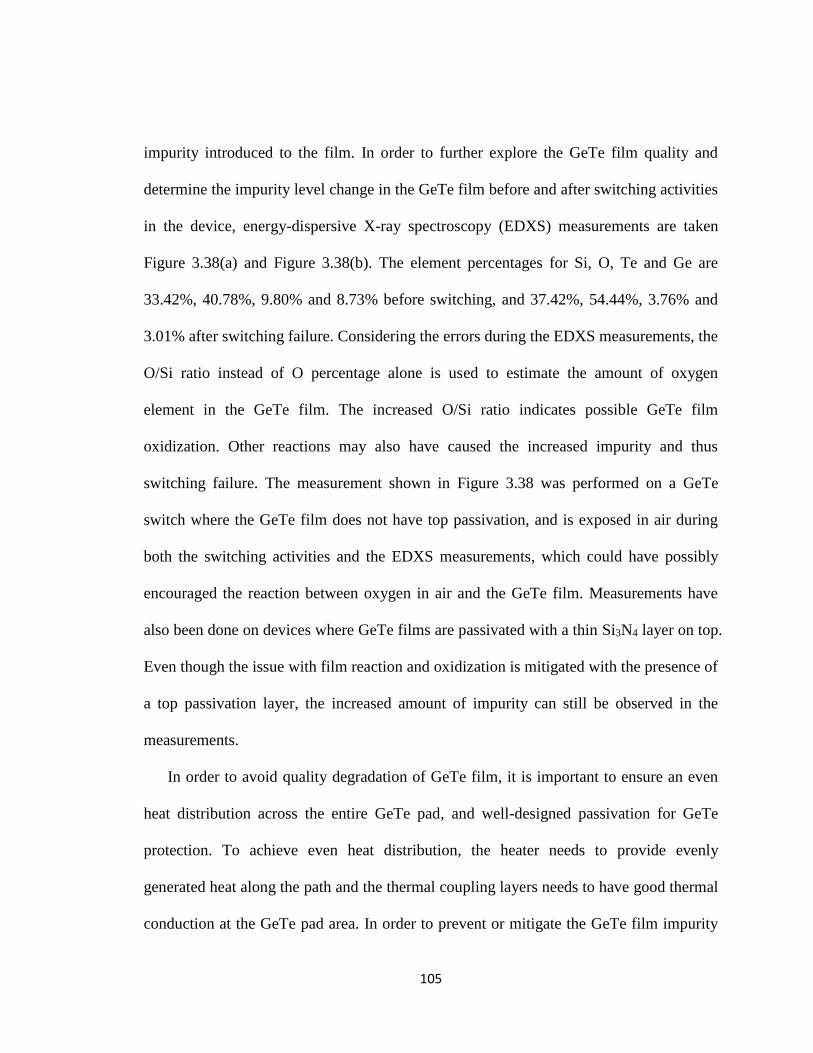
105
impurity introduced to the film. In order to further explore the GeTe film quality and
determine the impurity level change in the GeTe film before and after switching activities
in the device, energy-dispersive X-ray spectroscopy (EDXS) measurements are taken
Figure 3.38(a) and Figure 3.38(b). The element percentages for Si, O, Te and Ge are
33.42%, 40.78%, 9.80% and 8.73% before switching, and 37.42%, 54.44%, 3.76% and
3.01% after switching failure. Considering the errors during the EDXS measurements, the
O/Si ratio instead of O percentage alone is used to estimate the amount of oxygen
element in the GeTe film. The increased O/Si ratio indicates possible GeTe film
oxidization. Other reactions may also have caused the increased impurity and thus
switching failure. The measurement shown in Figure 3.38 was performed on a GeTe
switch where the GeTe film does not have top passivation, and is exposed in air during
both the switching activities and the EDXS measurements, which could have possibly
encouraged the reaction between oxygen in air and the GeTe film. Measurements have
also been done on devices where GeTe films are passivated with a thin Si3N4 layer on top.
Even though the issue with film reaction and oxidization is mitigated with the presence of
a top passivation layer, the increased amount of impurity can still be observed in the
measurements.
In order to avoid quality degradation of GeTe film, it is important to ensure an even
heat distribution across the entire GeTe pad, and well-designed passivation for GeTe
protection. To achieve even heat distribution, the heater needs to provide evenly
generated heat along the path and the thermal coupling layers needs to have good thermal
conduction at the GeTe pad area. In order to prevent or mitigate the GeTe film impurity
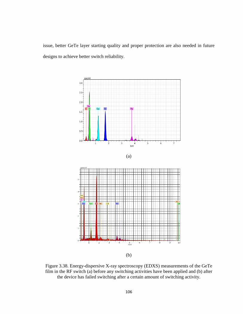
106
issue, better GeTe layer starting quality and proper protection are also needed in future
designs to achieve better switch reliability.
(a)
(b)
Figure 3.38. Energy-dispersive X-ray spectroscopy (EDXS) measurements of the GeTe
film in the RF switch (a) before any switching activities have been applied and (b) after
the device has failed switching after a certain amount of switching activity.

107
3.4.2. Switch Reliability Evaluation
In order to evaluate the reliability of the GeTe RF switch under frequent switching
activities, a repeated switch measurement has been performed. This process includes
turning the switch ON and OFF repeatedly by applying heating voltage pulses, and record
the resistance of the switch after each switching activity. If the switch becomes very
difficult or impossible to turn ON or OFF in the process, the measurement is stopped. In
this measurement the GeTe switch with indirect heating method is used.
Figure 3.39. Resistance response of the indirectly heated switch measured with repeated
switching activities using thermal actuations.
The reliability measurements have been performed on different batches of fabricated
devices as well as different devices within the same batches. The results show a great
0 50 100 150
10-1
100
101
102
103
104
105
Resis
tance (
Ohm
)
Number of Heating Pulses
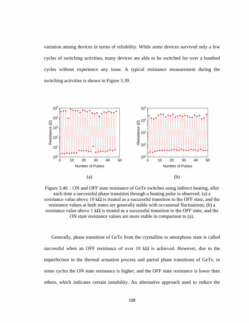
108
variation among devices in terms of reliability. While some devices survived only a few
cycles of switching activities, many devices are able to be switched for over a hundred
cycles without experience any issue. A typical resistance measurement during the
switching activities is shown in Figure 3.39.
(a) (b)
Figure 3.40. : ON and OFF state resistance of GeTe switches using indirect heating, after
each time a successful phase transition through a heating pulse is observed. (a) a
resistance value above 10 kΩ is treated as a successful transition to the OFF state, and the
resistance values at both states are generally stable with occasional fluctuations; (b) a
resistance value above 1 kΩ is treated as a successful transition to the OFF state, and the
ON state resistance values are more stable in comparison to (a).
Generally, phase transition of GeTe from the crystalline to amorphous state is called
successful when an OFF resistance of over 10 kΩ is achieved. However, due to the
imperfection in the thermal actuation process and partial phase transitions of GeTe, in
some cycles the ON state resistance is higher, and the OFF state resistance is lower than
others, which indicates certain instability. An alternative approach used to reduce the
0 10 20 30 40 5010
0
101
102
103
104
105
Re
sis
tan
ce
(Ω
)
Number of Pulses
0 10 20 30 40 5010
0
101
102
103
104
Resis
tance (Ω
)
Number of Pulses

109
heater power consumption and increase switching cycles is to apply enough power to get
an OFF state resistance of above 1 kΩ. Since the isolation in the OFF state is mostly
dependent on the capacitance between the RF terminals, a relatively lower resistance of 1
kΩ will not greatly affect the isolation of the switch, but this makes the phase transitions
much easier for an extended number of switching cycles. The resistance responses of
these two types of measurements are shown in Figure 3.40.
3.5. Summary
In this chapter, chalcogenide phase change materials, especially GeTe, in RF
switching applications have been discussed. The two types of four-terminal GeTe RF
switches are presented in detail, including the design and fabrication process as well as
the performance evaluation and reliability analysis. Overall, GeTe has shown its
promising potential in the application of reconfigurable RF modules and systems. A brief
performance comparison among different RF switching technologies is provided in Table
3.3.
In Table 3.3, measured results of two types of GeTe RF switch designs from this
work and another reported GeTe based phase change switch design are included, along
with other technologies such as RF MEMS, SOI/SOS and pHEMT. It is shown that GeTe
RF switches have competitive performance overall compared to existing technologies,
with a wider operating frequency range and high RF performance at high frequencies
compared to most solid-state based switches. Compared to RF MEMS switches, although
GeTe switches are generally showing a lower cut-off frequency, they offer the advantage

110
of smaller size, lower operating DC voltage, good scalability and integration
compatibility, as well as easier fabrication and lower cost. While GeTe switches are
showing higher power consumption for switching activities than other designs, the
switching power is pulse based and therefore the total energy budget can be well
managed.
Table 3.3. Comparison of RF switch designs using different technologies.
Technology
GeTe
(Direct
Heating
Scheme)
GeTe
(Indirect
Heating
Scheme)
GeTe
(Indirect
Heating
Scheme)
RF
MEMS 0.18 m
SOI
0.25 m
SOS
0.15m
GaAs
pHEMT
Example(s)
This
work [64]
[65]
This
work
[72] [75]
[63] [76] [20] [12] [77] [11] [78]
Operating
Frequency
Tested
Up to 20
GHz
Up to 20
GHz
Up to 40
GHz
Up to 50
GHz
Up to 10
GHz
Up to 2.5
GHz
Up to 0.9
GHz
Insertion
Loss
0.5 dB
@
20 GHz
0.3 dB
@
20 GHz
0.2 dB
@
20 GHz
0.2 dB
@
50 GHz
<1.5 dB
@
10 GHz
<1 dB
@
2.5 GHz
0.25 dB
@
9 GHz
Isolation
18 dB
@
20 GHz
11 dB
@
20 GHz
15 dB
@
20 GHz
25 dB
@
50 GHz
17 dB
@
10 GHz
- -
fco >4 THz >5.6 THz >12.5
THz >20 THz
0.637
THz
0.355
THz
0.366
THz
Switching
Speed
(Typically) <3 s <2 s - ~1 s 0.1-1 s 0.1-1 s ~1 s
Switching
Power
(Typically)
<100
mW
(Pulse)
<2 W
(Pulse)
<2 W
(Pulse)
0 static
power
W –
mW
(static)
~W –
mW
(static)
~mW
(static)
Control
Voltage <10 V <20 V - <100 V ~2.5 V ~4 V ~5 V
Power
Handling
(Typically)
>>20
dBm
>>20
dBm >35 dBm
<30
dBm
30 – 50
dBm
30 – 50
dBm
20 – 0
dBm
Size
(Typically) <500 m2 <500 m2 <500 m2 >10 mm2
0.1 – 10
mm2
0.1 – 10
mm2 ~10 mm2
Cost Low Low Low Medium-
high Very low Low
Low-
Medium

111
CHAPTER 4 Reconfigurable Bandpass Filter Using GeTe RF Switches
A reconfigurable bandpass filter for X-band applications has been implemented using
our GeTe-based phase change switches. The design methods and performance
measurements have been reported in [79]. This filter has been implemented as a proof of
concept to demonstrate applicability of GeTe switches in frequency agile RF modules,
showing promising performance compared to existing reconfigurable bandpass filter
designs at a similar frequency range.
4.1. Motivation and Background
There is a high demand for compact and low-loss reconfigurable filters for various
advanced wireless applications. A number of common applications of reconfigurable
filters can be named including cognitive radios, modern transceivers, anti-jamming
communication systems, etc. [80]. With reconfigurable filters, wireless communication
systems that require multiple operating frequency bands can be implemented with smaller
size and reduced cost compared to conventional systems using multiple single-frequency
filters. Compared to low-pass or high-pass filters, bandpass filters provide an improved
signal-to-noise ratio (SNR) and better rejection of out-of-band signals [81].
There have been various designs reported for implementing tunable or reconfigurable
filters. The frequency tuning for such devices is achieved electronically by technologies
such as solid-state varactors or switches [82], RF MEMS switches or capacitors [83],
112
magnetic or ferroelectric components [84, 85, 86], etc. Solid state tuning elements such
as varactors and switches are the commercialized type of devices used in tunable or
reconfigurable filters. While they are commonly used in wireless systems with good
reliability and compatibility for integration, they tend to have relatively high losses (high
electrical resistance), especially at high frequencies (>10 GHz) and linearity issues
limiting their application areas. MEMS tuning elements, such as electrostatic switches,
are proven to have much better insertion loss and isolation performance across a wide
frequency range [20]. They typically use suspended or other types of mechanical
structures to switch between states, and provide very low contact resistance when
switched on because of the direct metal contact, and extremely high resistance when
switched off. However, a high DC voltage (usually more than 20 V) is typically required
for pull-in and a constant voltage need to be applied to maintain the ON state. In addition,
due to their suspended mechanical structures, the fabrication process of such devices is
usually complicated and has yield and reliability issues.
The X band, which is defined as the frequency range from 7.0 to 11.2 GHz (or 8.0 to
12.0 GHz according to IEEE standards), is commonly used by civil, military and
government radar applications such as weather monitoring, air traffic control, defense
tracking, law enforcement, etc. There are several reported designs of X band and near X
band planar tunable filters that provide good performance using MEMS switches [83],
yttrium iron garnet/gadolinium gallium garnet (YIG/GGG) [85], ferroelectric barium-
strontium-titanate (BST) capacitors [86], and vanadium oxide (VOx) switches [87] as the
tuning elements. The tunable bandpass filter design reported in [83] is based on a 2-bit

113
tuning structure using ohmic contact MEMS switches that provide frequency tuning
ranges of 20% and 44% at the frequencies between 12 GHz and 15 GHz with two
different device sets. The fabricated devices are measured to have a fractional bandwidth
of 5.7% and an insertion loss lower than 3.2 dB at all states, with an unloaded quality
factor of better than 75. The work reported in [85] utilizes YIG/GGG layers on a
RT/Duroid substrate to achieve frequency tuning in the X-band. This filter operates at
different center frequencies from 8 GHz to 12 GHz, with 3-dB fractional bandwidths of
approximately 10% to 14%, and an insertion loss of 2.5 dB. The design reported in [86]
is a two-pole microstrip line based tunable filter using ferroelectric BST capacitors as the
tuning elements with a center frequency around 10 GHz and a constant fractional
bandwidth of 8.5% within the tuning range of approximately 8.3%. This reported design
provides an insertion loss lower than 2.7 dB. The work reported in [87] presents a
reconfigurable bandpass filter that integrates VOx microwave switches into a spilt ring
resonator based design. The VOx is a relatively new type of material for RF applications
that provides fast and reversible semiconductor-to-metal transition, and is used in
microwave switches to achieve reconfigurability. This work shows a filter insertion loss
within 5 dB and a 3-dB bandwidth of 12-13%. The challenge with VOx switches is that
they have a low power handling capability and comparably poor linearity. They also
require a constant bias to stay in one state. In [79], we presented a reconfigurable
bandpass filter for X-band applications using a new tuning technique. Here, the design
and fabrication process are discussed, and the performance of filters is analyzed and
compared to the designs mentioned above.
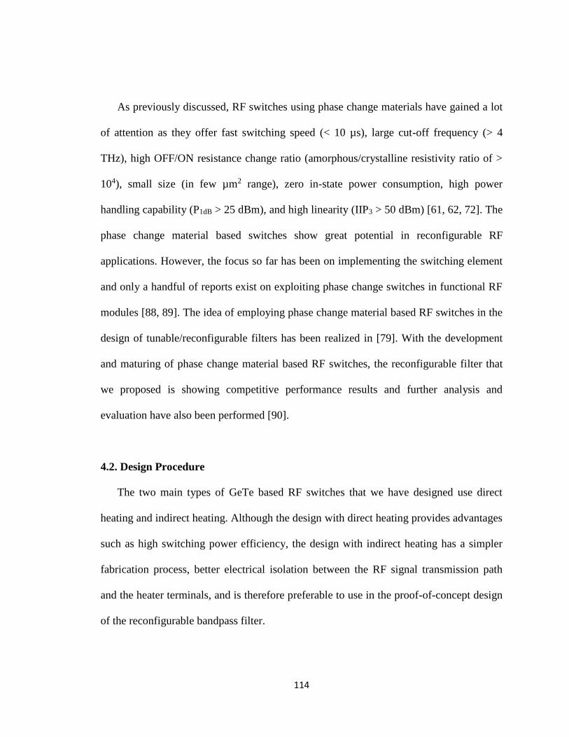
114
As previously discussed, RF switches using phase change materials have gained a lot
of attention as they offer fast switching speed (< 10 µs), large cut-off frequency (> 4
THz), high OFF/ON resistance change ratio (amorphous/crystalline resistivity ratio of >
104), small size (in few µm2 range), zero in-state power consumption, high power
handling capability (P1dB > 25 dBm), and high linearity (IIP3 > 50 dBm) [61, 62, 72]. The
phase change material based switches show great potential in reconfigurable RF
applications. However, the focus so far has been on implementing the switching element
and only a handful of reports exist on exploiting phase change switches in functional RF
modules [88, 89]. The idea of employing phase change material based RF switches in the
design of tunable/reconfigurable filters has been realized in [79]. With the development
and maturing of phase change material based RF switches, the reconfigurable filter that
we proposed is showing competitive performance results and further analysis and
evaluation have also been performed [90].
4.2. Design Procedure
The two main types of GeTe based RF switches that we have designed use direct
heating and indirect heating. Although the design with direct heating provides advantages
such as high switching power efficiency, the design with indirect heating has a simpler
fabrication process, better electrical isolation between the RF signal transmission path
and the heater terminals, and is therefore preferable to use in the proof-of-concept design
of the reconfigurable bandpass filter.

115
This filter prototype is designed to target the X-band frequencies for military
communication applications with an uplink band frequency of 8.15 GHz and a downlink
band frequency of 7.5 GHz. For both bands, the 3-dB bandwidth is targeted at 500 MHz,
and the target insertion loss for both bands is 4 dB or lower. The main structure of the
filter is implemented with microstrip lines, and the reconfigurability of the filter is
realized using the GeTe RF switches with indirect heating that are integrated on chip.
The filter is based on coupled microstrip line resonators, which uses an open-loop λ/2
microstrip line configuration. The frequency band selection is realized through shifting
the center frequency of the resonators with switchable capacitors (open-circuited
microstrip line stubs). The capacitor switching is achieved using the GeTe based RF
switches. The external coupling of the filter is achieved by coupled feed lines at the
terminals. The detailed schematic of the filter structure is shown in Figure 4.1.
In order to obtain the targeted constant absolute bandwidth (CABW) of 500 MHz
from the specifications, calculations and simulations are done to tune the element
parameters of the filter. The design procedure starts based on a low-pass Butterworth
filter prototype, with elements g0, g1, g2 and g3. According to the target center frequencies
(𝑓1 and 𝑓2) and the 3-dB fractional bandwidth (Δ), one can calculate the corresponding
required external quality factor ( 𝑄𝑒𝑥𝑡 ) and the coupling coefficients ( 𝑘12 ) of the
microstrip line resonators. The calculations can be done with Equations (4.1)-(4.3). In
Equations (4.1a)-(4.1d), the admittance parameters [𝑌] correspond to the impedance
parameters [𝑍], and the constant parameters used are listed in Table 4.1.
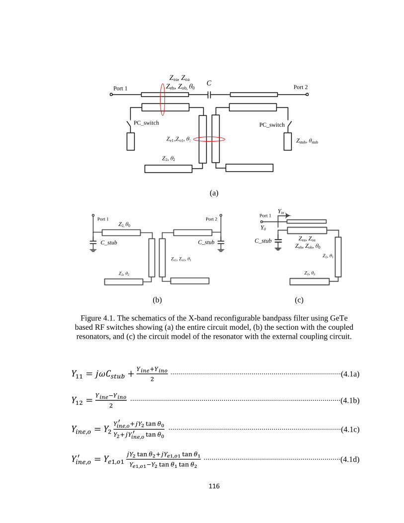
116
(a)
(b) (c)
Figure 4.1. The schematics of the X-band reconfigurable bandpass filter using GeTe
based RF switches showing (a) the entire circuit model, (b) the section with the coupled
resonators, and (c) the circuit model of the resonator with the external coupling circuit.
𝑌11 = 𝑗𝜔𝐶𝑠𝑡𝑢𝑏 +𝑌𝑖𝑛𝑒+𝑌𝑖𝑛𝑜
2 ∙∙∙∙∙∙∙∙∙∙∙∙∙∙∙∙∙∙∙∙∙∙∙∙∙∙∙∙∙∙∙∙∙∙∙∙∙∙∙∙∙∙∙∙∙∙∙∙∙∙∙∙∙∙∙∙∙∙∙∙∙∙∙∙∙∙∙∙∙∙∙∙∙∙∙∙∙∙∙∙∙∙∙∙∙∙(4.1a)
𝑌12 =𝑌𝑖𝑛𝑒−𝑌𝑖𝑛𝑜
2 ∙∙∙∙∙∙∙∙∙∙∙∙∙∙∙∙∙∙∙∙∙∙∙∙∙∙∙∙∙∙∙∙∙∙∙∙∙∙∙∙∙∙∙∙∙∙∙∙∙∙∙∙∙∙∙∙∙∙∙∙∙∙∙∙∙∙∙∙∙∙∙∙∙∙∙∙∙∙∙∙∙∙∙∙∙∙∙∙∙∙∙∙∙∙∙∙∙∙∙∙∙∙∙∙∙∙(4.1b)
𝑌𝑖𝑛𝑒,𝑜 = 𝑌2𝑌𝑖𝑛𝑒,𝑜
′ +𝑗𝑌2 tan 𝜃0
𝑌2+𝑗𝑌𝑖𝑛𝑒,𝑜′ tan 𝜃0
∙∙∙∙∙∙∙∙∙∙∙∙∙∙∙∙∙∙∙∙∙∙∙∙∙∙∙∙∙∙∙∙∙∙∙∙∙∙∙∙∙∙∙∙∙∙∙∙∙∙∙∙∙∙∙∙∙∙∙∙∙∙∙∙∙∙∙∙∙∙∙∙∙∙∙∙∙∙∙∙∙∙∙∙∙∙∙(4.1c)
𝑌𝑖𝑛𝑒,𝑜′ = 𝑌𝑒1,𝑜1
𝑗𝑌2 tan 𝜃2+𝑗𝑌𝑒1,𝑜1 tan 𝜃1
𝑌𝑒1,𝑜1−𝑌2 tan 𝜃1 tan 𝜃2 ∙∙∙∙∙∙∙∙∙∙∙∙∙∙∙∙∙∙∙∙∙∙∙∙∙∙∙∙∙∙∙∙∙∙∙∙∙∙∙∙∙∙∙∙∙∙∙∙∙∙∙∙∙∙∙∙∙∙∙∙∙∙∙∙∙∙∙∙∙(4.1d)
Port 1
PC_switch
Port 2
PC_switch
Ze1 ,Zo1, θ1 Zstub, θstub
CZea, Zoa
Zeb, Zob, θ0
Z2, θ2
Port 1
Ze1, Zo1, θ1
Z2, θ0
Z2, θ2
C_stub C_stub
Port 2
Z2, θ2
C_stub
Port 1
Zea, Zoa
Zeb, Zob, θ0
Z2, θ1
Yin
Y0
117
𝐼𝑚[𝑌11(𝜔0)] = 0 ∙∙∙∙∙∙∙∙∙∙∙∙∙∙∙∙∙∙∙∙∙∙∙∙∙∙∙∙∙∙∙∙∙∙∙∙∙∙∙∙∙∙∙∙∙∙∙∙∙∙∙∙∙∙∙∙∙∙∙∙∙∙∙∙∙∙∙∙∙∙∙∙∙∙∙∙∙∙∙∙∙∙∙∙∙∙∙∙∙∙∙∙∙∙∙∙∙∙∙∙∙(4.2a)
𝐼𝑚[𝑌12(𝜔0)]
𝑏=
Δ
√𝑔1𝑔2= 𝑘12, 𝑏 =
𝜔02
𝜕𝐼𝑚[𝑌11(𝜔0)]
𝜕𝜔 ∙∙∙∙∙∙∙∙∙∙∙∙∙∙∙∙∙∙∙∙∙∙∙∙∙∙∙∙∙∙∙∙∙∙∙∙∙∙∙∙∙∙∙∙∙∙∙∙∙∙∙(4.2b)
𝑄𝑒𝑥𝑡 =𝑏
𝑌0=
𝜔02𝑌0
𝜕𝐼𝑚[𝑌𝑖𝑛(𝜔0)]
𝜕𝜔=
𝑔1𝑔2
Δ ∙∙∙∙∙∙∙∙∙∙∙∙∙∙∙∙∙∙∙∙∙∙∙∙∙∙∙∙∙∙∙∙∙∙∙∙∙∙∙∙∙∙∙∙∙∙∙∙∙∙∙∙∙∙∙∙∙∙∙∙∙∙∙∙∙∙∙∙∙∙∙∙(4.3)
Table 4.1. Constant parameters used in the design calculations.
Parameter Value
𝑍𝑒1 37 Ω
𝑍𝑜1 23.3 Ω
𝑍2 33Ω
𝜃0 55°
𝜃1 23°
𝜃2 95°
Figure 4.2. Desired and achieved coupling coefficients of the coupled resonators in the
filter as a function of frequency.
7.0 7.2 7.4 7.6 7.8 8.0 8.2 8.40.035
0.040
0.045
0.050
0.055
Co
up
lin
g c
oef
fici
ent
(k1
2)
Frequency (GHz)
Desired k12
for CABW of 500 MHz
Calculated k12
for CABW of 500 MHz
118
The admittance parameters 𝑌11 and 𝑌12 are first calculated based on Equations (4.1a) -
(4.1d). In order to achieve constant absolute bandwidth (CABW), the coupling coefficient
conditions are required to satisfy Equation (4.2b) across the entire tuning range and the
external Q should satisfy Equations (4.3) [91]. The required and calculated coupling
coefficient 𝑘12 for a constant bandwidth of 500 MHz at the two target center frequencies
are plotted in Figure 4.2.
In summary, the design procedure of the phase change reconfigurable filter is as
following: 1) Given the filter specifications, including the center frequencies (𝑓1 = 7.5
GHz, 𝑓2 = 8.15 GHz) and the absolute bandwidth (BW3dB), we obtain the desired values
of external quality factors and the coupling coefficients by using Equations (4.1)- (4.3). 2)
Then, we design the half-wavelength resonators to operate at 𝑓1 . The frequency 𝑓2 is
mainly determined by the length of resonators, i.e., (l1+l2+l3). The lower passband
frequency f1 is mainly determined by the dimensions of stub, i.e., (w3, l4). The mixed
coupling between resonators is realized using coupling lines (l2). Once the line width w1
and the length l2 are fixed, the coupling coefficients depend on the gap s. By changing
impedances of the coupled lines (Ze1, Zo1 and θ1), k12 can be synthesized with different
slopes for low-band (𝑓1) and high-band (𝑓2) modes. Then, the initial values of w1, l1, l2, l3
and s can be obtained. 3) Once the line width w1 and the line length l1 are fixed, the
external quality factor 𝑄𝑒𝑥𝑡 is controlled by the gap g0 and the width w2. 4) The GeTe
switch design follows the procedure outlined in [72]. 5) Finally, using the initial
parameters from the above-mentioned steps, we perform full-wave simulations using
ANSYS HFSS to take all parasitic effects into account and we optimize and finalize the
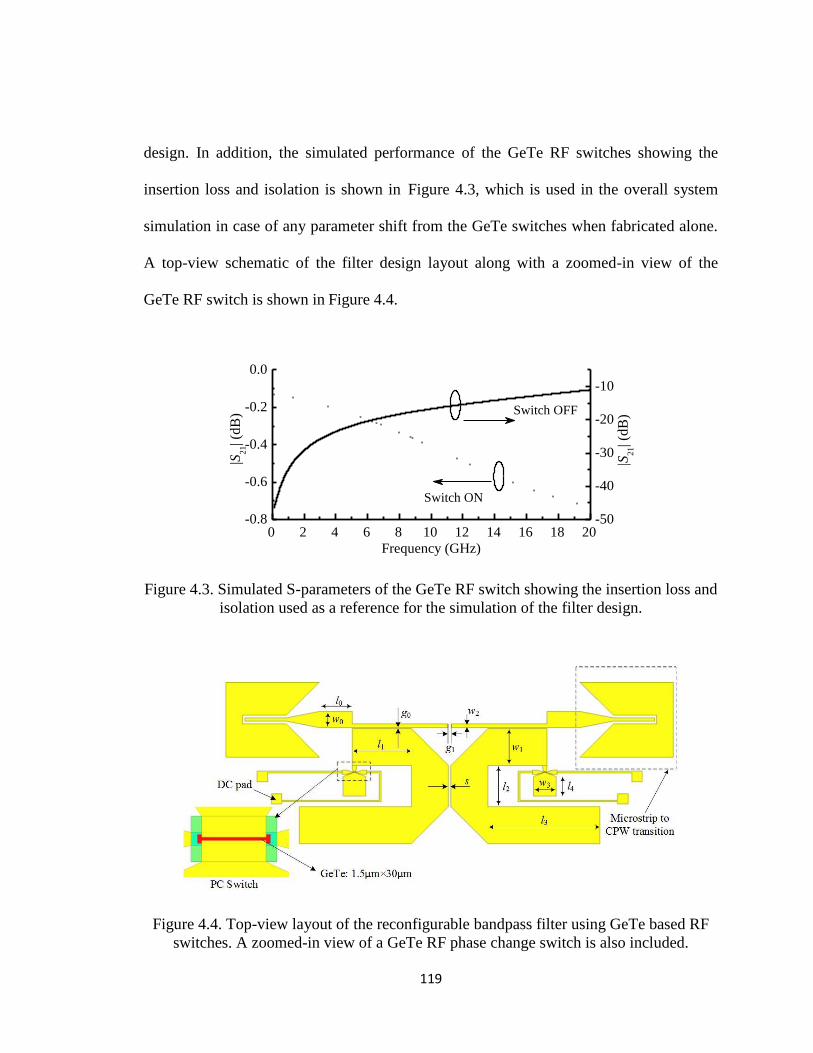
119
design. In addition, the simulated performance of the GeTe RF switches showing the
insertion loss and isolation is shown in Figure 4.3, which is used in the overall system
simulation in case of any parameter shift from the GeTe switches when fabricated alone.
A top-view schematic of the filter design layout along with a zoomed-in view of the
GeTe RF switch is shown in Figure 4.4.
Figure 4.3. Simulated S-parameters of the GeTe RF switch showing the insertion loss and
isolation used as a reference for the simulation of the filter design.
Figure 4.4. Top-view layout of the reconfigurable bandpass filter using GeTe based RF
switches. A zoomed-in view of a GeTe RF phase change switch is also included.
0 2 4 6 8 10 12 14 16 18 20-0.8
-0.6
-0.4
-0.2
0.0
Switch OFF
|S21| (
dB
)
|S21| (
dB
)
Frequency (GHz)
Switch ON
-50
-40
-30
-20
-10

120
4.3. Fabrication Process
The fabrication process of the GeTe RF phase change switches using indirect heating
has been discussed in the previous chapter. Since the reconfigurable bandpass filter
consists of both microstrip line coupled resonators and GeTe RF switches, a fabrication
process is designed to integrate the GeTe switches on chip with the microstrip line
structures. The cross-sectional schematic of the device is shown in Figure 4.5.
Figure 4.5. Cross-sectional schematic showing structure of the filter design. The
microstrip lines share the gold layer from the GeTe switches. This diagram is intended to
show the layer configuration, and does not reflect the actual device layout. The device
layout is shown in Figure 4.4.
The fabrication of the GeTe RF switch based reconfigurable bandpass filter is
performed on a double-side polished high-resistivity Si substrate for its high dielectric
constant, high thermal conductivity, low substrate loss and compatibility with the GeTe
RF switch fabrication processes. The detailed fabrication process flow is shown in Figure
4.6. The process starts with a back side coating of Au layer with a thickness of 500 nm to
form the back plate. The front side process is similar to the GeTe RF switch process
when fabricated standing alone. A SiO2 passivation layer with a thickness of 2 m is
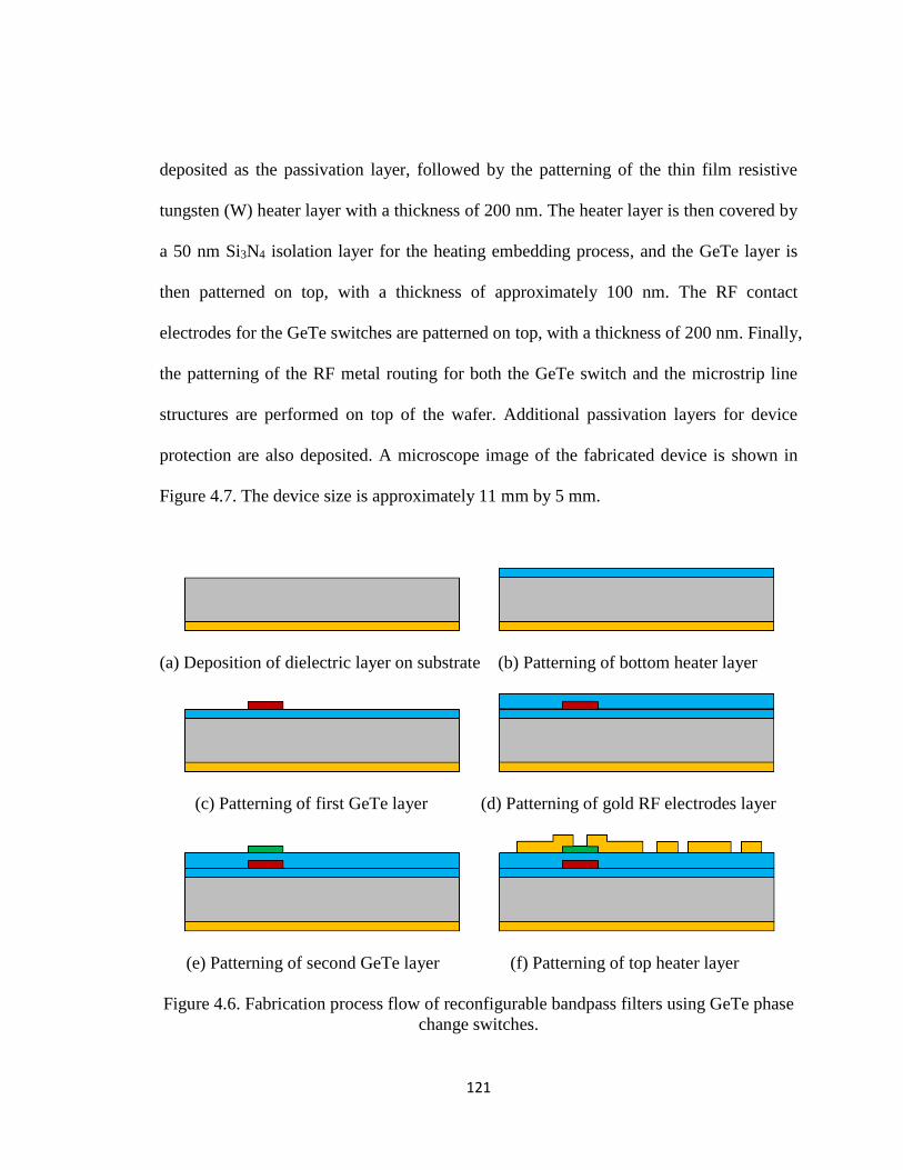
121
deposited as the passivation layer, followed by the patterning of the thin film resistive
tungsten (W) heater layer with a thickness of 200 nm. The heater layer is then covered by
a 50 nm Si3N4 isolation layer for the heating embedding process, and the GeTe layer is
then patterned on top, with a thickness of approximately 100 nm. The RF contact
electrodes for the GeTe switches are patterned on top, with a thickness of 200 nm. Finally,
the patterning of the RF metal routing for both the GeTe switch and the microstrip line
structures are performed on top of the wafer. Additional passivation layers for device
protection are also deposited. A microscope image of the fabricated device is shown in
Figure 4.7. The device size is approximately 11 mm by 5 mm.
(a) Deposition of dielectric layer on substrate (b) Patterning of bottom heater layer
(c) Patterning of first GeTe layer (d) Patterning of gold RF electrodes layer
(e) Patterning of second GeTe layer (f) Patterning of top heater layer
Figure 4.6. Fabrication process flow of reconfigurable bandpass filters using GeTe phase
change switches.
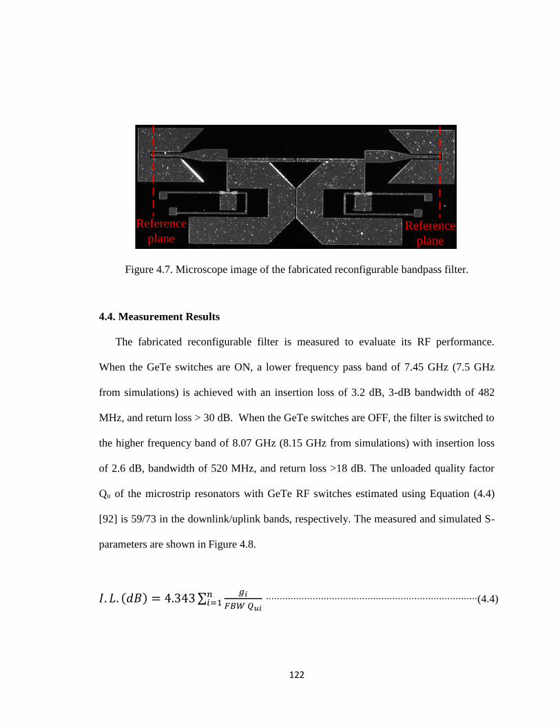
122
Figure 4.7. Microscope image of the fabricated reconfigurable bandpass filter.
4.4. Measurement Results
The fabricated reconfigurable filter is measured to evaluate its RF performance.
When the GeTe switches are ON, a lower frequency pass band of 7.45 GHz (7.5 GHz
from simulations) is achieved with an insertion loss of 3.2 dB, 3-dB bandwidth of 482
MHz, and return loss > 30 dB. When the GeTe switches are OFF, the filter is switched to
the higher frequency band of 8.07 GHz (8.15 GHz from simulations) with insertion loss
of 2.6 dB, bandwidth of 520 MHz, and return loss >18 dB. The unloaded quality factor
Qu of the microstrip resonators with GeTe RF switches estimated using Equation (4.4)
[92] is 59/73 in the downlink/uplink bands, respectively. The measured and simulated S-
parameters are shown in Figure 4.8.
𝐼. 𝐿. (𝑑𝐵) = 4.343 ∑𝑔𝑖
𝐹𝐵𝑊 𝑄𝑢𝑖
𝑛𝑖=1 ∙∙∙∙∙∙∙∙∙∙∙∙∙∙∙∙∙∙∙∙∙∙∙∙∙∙∙∙∙∙∙∙∙∙∙∙∙∙∙∙∙∙∙∙∙∙∙∙∙∙∙∙∙∙∙∙∙∙∙∙∙∙∙∙∙∙∙∙∙∙∙∙∙∙∙∙∙(4.4)
Reference
planeReference
plane
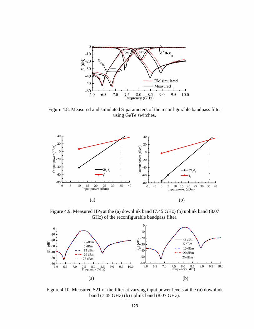
123
Figure 4.8. Measured and simulated S-parameters of the reconfigurable bandpass filter
using GeTe switches.
(a) (b)
Figure 4.9. Measured IIP3 at the (a) downlink band (7.45 GHz) (b) uplink band (8.07
GHz) of the reconfigurable bandpass filter.
(a) (b)
Figure 4.10. Measured S21 of the filter at varying input power levels at the (a) downlink
band (7.45 GHz) (b) uplink band (8.07 GHz).
0 5 10 15 20 25 30 35 40-80
-60
-40
-20
0
20
40
Outp
ut
pow
er (
dB
m)
Input power (dBm)
2f1-f
2
f1
-10 -5 0 5 10 15 20 25 30 35 40-80
-60
-40
-20
0
20
40O
utp
ut
pow
er (
dB
m)
Input power (dBm)
2f1-f
2
f1
6.0 6.5 7.0 7.5 8.0 8.5 9.0 9.5 10.0-60
-50
-40
-30
-20
-10
0
|S21| (
dB
)
Frequency (GHz)
-5 dBm
5 dBm
15 dBm
20 dBm
25 dBm
6.0 6.5 7.0 7.5 8.0 8.5 9.0 9.5 10.0-60
-50
-40
-30
-20
-10
0
|S21| (d
B)
Frequency (GHz)
-5 dBm
5 dBm
15 dBm
20 dBm
25 dBm
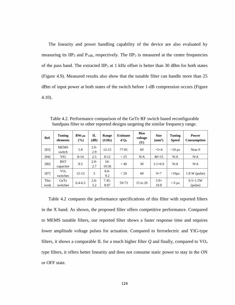
124
The linearity and power handling capability of the device are also evaluated by
measuring its IIP3 and P1dB, respectively. The IIP3 is measured at the center frequencies
of the pass band. The extracted IIP3 at 1 kHz offset is better than 30 dBm for both states
(Figure 4.9). Measured results also show that the tunable filter can handle more than 25
dBm of input power at both states of the switch before 1-dB compression occurs (Figure
4.10).
Table 4.2. Performance comparison of the GeTe RF switch based reconfigurable
bandpass filter to other reported designs targeting the similar frequency range.
Ref. Tuning
elements
BW3dB
(%)
IL
(dB)
Range
(GHz)
Estimate
d Qu
Bias
voltage
(V)
Size
(mm2)
Tuning
Speed
Power
Consumption
[83] MEMS
switch 5.8
2.6-
2.9 12-15 77-81 60 ~5×4 ~10 µs Near 0
[84] YIG 8-14 2.5 8-12 < 25 N/A 40×15 N/A N/A
[86] BST
capacitor 8.5
2.0-
2.7
10-
10.56 < 40 30 3.1×6.9 N/A N/A
[87] VOx
switches 12-13 5
8.6-
9.2 < 20 60 9×7 <10µs 1.8 W (pulse)
This
work
GeTe
switches 6.4-6.5
2.6-
3.2
7.45-
8.07 59-73 15 to 20
3.9×
10.8 < 6 µs
0.5~1.5W
(pulse)
Table 4.2 compares the performance specifications of this filter with reported filters
in the X band. As shown, the proposed filter offers competitive performance. Compared
to MEMS tunable filters, our reported filter shows a faster response time and requires
lower amplitude voltage pulses for actuation. Compared to ferroelectric and YIG-type
filters, it shows a comparable IL for a much higher filter Q and finally, compared to VOx
type filters, it offers better linearity and does not consume static power to stay in the ON
or OFF state.

125
CHAPTER 5 Conclusions and Future Directions
5.1. Thesis Contributions
The research work discussed in this thesis provides the following key contributions:
1. Investigation into properties of GeTe phase change material and its thermally
actuated phase transition activities.
This work combines the investigation of phase change materials in a
semiconductor physics perspective and exploration of phase change material
behaviors in RF applications based on testing and measurement results. A
literature summary of phase change material studies in the early stages has been
provided in the thesis, showing the progress from early discovery of disordered
semiconducting material consisting of Te, As, Si and Ge, to generalized
chalcogenide phase change material property study. Specifically, the study of
GeTe has been performed to explore the phase transition properties.
The comparison of electrical and optical properties between amorphous and
crystalline GeTe films have been performed, assisted by SEM and TEM imaging,
XRD measurement, EDS material study, as well as optical ellipsometry
measurements. The crystallization and amorphization processes of GeTe films
have also been explored with varying parameters and conditions to determine the
optimal process to achieve most complete phase transitions. This study

126
contributed to a step towards optimization of GeTe-based RF phase change ohmic
switches in terms of RF performance and switching reliability.
2. Development of GeTe-based RF phase change ohmic switches with the four-terminal
structures.
Based on the previously proposed GeTe-based RF phase change ohmic switch
with the two-terminal structure, a new four-terminal structure has been devised
and developed. While inheriting the direct heating method from the two-terminal
structure, the four-terminal switch is able to separate the thermal actuation pulses
from the RF signals. With this structure, the RF signal transmission path and the
heating path can be separately optimized for their functionality, while maintaining
decent switching power efficiency. The device has been implemented and
optimized with good RF performance, with an insertion loss less than 0.5 dB and
an isolation above 18 dB from DC to 20 GHz, showing a figure-of-merit cut-off
frequency over 4 THz. This indicates competitive performance compared to
existing RF switch designs with solid-state or MEMS technology. The switch has
also been verified to have good linearity and power handling capability.
A four-terminal structure with indirect heating scheme for the GeTe-based RF
phase change ohmic switch has also been developed. Compared to the direct
heating scheme, this indirect heating scheme results in a simplified device
structure and fabrication process. The heater embedding process for this device
structure ensures electrical isolation between the RF and heater terminals, which
minimizes RF signal leakage into the heater terminals, and therefore provides

127
better integration compatibility with other modules within certain RF systems.
Since the resistive heater path in this structure is relatively independent from the
GeTe connection of the switch, it is possible to build switch stacks where the
GeTe switches can be connected in series or parallel sharing a single resistive
heater for better voltage or current handling capability. The GeTe RF switch with
indirect heating method has also been fabricated and tested, showing good
performance. The optimized design shows an insertion loss within 0.3 dB and an
isolation above 11 dB from DC to 20 GHz, indicating a figure-of-merit cut-off
frequency over 5.6 THz.
A series of nano/micro-fabrication processes have been developed for GeTe-
based RF switches. A plasma induced sputtering process has been characterized
for GeTe thin-film deposition with a single GeTe target. The detailed parameters
for the sputtering process has been optimized for best film quality of GeTe, which
is essential for successful crystallization and reliable phase transitions of GeTe
vias in RF switches. Two different patterning methods for GeTe films using lift-
off and plasma etching, respectively, have been developed and compared in terms
of film and pattern quality. Depending on the device structure, fabrication process
and applications, both patterning methods have been used and a process has been
characterized for both methods. Other fabrication process steps, including the
GeTe-metal contact characterization, the heater embedding process, and surface
polishing and cleaning process have also been characterized to yield an optimized
switch performance.

128
A thermoelectric modeling method that was previously developed has been used
for the GeTe RF switches with both direct heating and indirect heating to relate
the thermal and electrical properties of the devices. The model analyzes the
impact of RF signals to the switches when operated at high RF power levels in
order to predict potential issues including self-actuation, non-linearity, and limited
power handling capability. Corresponding measurements have been taken to
verify good accuracy of the modeling method.
Reliability and breakdown analysis of the GeTe switches have been performed.
Repeated switching activities have been applied to the devices under test to
evaluate the stability and reliability of the GeTe RF switches. Upon switching
failure, the device is investigated to determine the cause for breakdown. Common
reasons for device switching failure have been identified such as the heater
breakdown, GeTe material fatigue and oxidation, etc. High-resolution imaging
techniques including SEM and TEM have been used to facilitate the analysis.
3. GeTe Switches in Reconfigurable RF Applications
A reconfigurable bandpass filter for the X-band communication applications has
been implemented using GeTe-based RF switches as the reconfigurable elements.
An integrated fabrication process has been developed for the GeTe switches to be
fabricated on chip with the microstrip line coupled-resonator based filter. The RF
measurement results of the filter shows promising performance, and a comparison
among novel designs of reconfigurable/tunable filters using technologies such as
129
MEMS, ferroelectric, and VO2 is also provided to evaluate the potential and
advantage of GeTe-based switches in reconfigurable RF applications.
5.2. Future Research Directions
The research work in this thesis has contributed to better understanding of material of
GeTe phase change material property at radio frequencies, the development of high-
performance RF switches using GeTe, and their applications in reconfigurable RF
systems. Based on the results achieved and issues discovered during the course of this
research, possible directions for future research are suggested below.
5.2.1. GeTe Atomistic Structure Modeling and Analysis
Although a number of different possible atomistic structures of crystalline GeTe has
been proposed facilitated by high-resolution TEM imaging and X-ray diffraction
measurements [54, 59], it is still not completely clear how the crystalline structures
within thin-film GeTe is formed, and what exact structures they possess given different
crystallization conditions. According to our findings, the properties of GeTe films (and
also phase change materials in general) can be significantly process dependent, and
because of that, different reported material study results can been found when the film
preparation and annealing processes are performed in different works under different
conditions. Even though the GeTe film study and phase transition analysis in this work
has resulted in findings that agree with other reported works in terms of general material
behavior and trends, the exact numbers such as electrical and optical parameters,
130
crystallization temperature, phase transition speed, etc. are not always the same. It can be
reasonably assumed that the formation of the crystalline structure within the GeTe films
during the crystallization process is not entirely the same when performed under different
setups, and the differences in the crystallization and amorphization process have resulted
in differences in electrical and optical properties of the GeTe films.
For the reasons mentioned above, it is very useful to further investigate the exact
atomistic structure of the crystalline GeTe films and the formation process of the GeTe
crystal. From our TEM imaging results, it has been noted that the GeTe films deposited
and crystallized following our process steps exhibit a poly-crystalline structure, with
different crystalline volumes showing different lattice orientations. But it is not known if
the different crystalline volumes also have a structural difference other than an
orientation difference. A better understanding of the crystalline structure can help with
the optimization of the annealing process, obtaining GeTe films with better crystallinity,
which will help improve the performance of GeTe-based RF switches.
5.2.2. Performance Improvement of GeTe RF Switches
Further performance and reliability improvement of the GeTe based RF switches is
essential to their applications in reconfigurable RF modules. Some existing designs of
GeTe-based RF switches reported in the recent years have been modified for performance
improvements through both structural modifications and fabrication process refinement
[93, 94, 95, 96, 76]. Future research regarding further performance improvement of GeTe

131
RF switches continuing from this thesis can be focused on the exploration of structural
variations of the devices and further fabrication process enhancement.
5.2.2.1. Structural Variations
The two main structures of the four-terminal GeTe-based RF phase change switches
discussed in this thesis use the direct heating and indirect heating schemes. The structure
of both types of devices can be varied in terms of layer configuration and terminal
placement. Such variations of the devices can help compare the performance in terms of
RF operation and switching activities.
Figure 5.1. An alternative structure of the four-terminal GeTe based RF ohmic switch
using direct heating with two heater terminals laterally connected and two RF terminals
vertically connected by the GeTe via.
For the direct heating scheme, the previously discussed structure of the GeTe
switches consists of a laterally connected RF signal transmission path and a vertically
connected heater path. This in-line structure is designed for low-resistance RF metal
contact out of fabrication process considerations, since the two RF electrodes in this
structure is symmetrical and RF contact metals stepping over a thick layer are avoided.
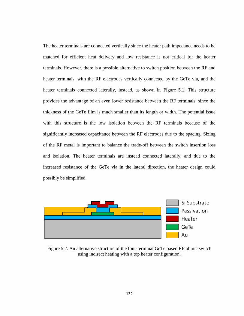
132
The heater terminals are connected vertically since the heater path impedance needs to be
matched for efficient heat delivery and low resistance is not critical for the heater
terminals. However, there is a possible alternative to switch position between the RF and
heater terminals, with the RF electrodes vertically connected by the GeTe via, and the
heater terminals connected laterally, instead, as shown in Figure 5.1. This structure
provides the advantage of an even lower resistance between the RF terminals, since the
thickness of the GeTe film is much smaller than its length or width. The potential issue
with this structure is the low isolation between the RF terminals because of the
significantly increased capacitance between the RF electrodes due to the spacing. Sizing
of the RF metal is important to balance the trade-off between the switch insertion loss
and isolation. The heater terminals are instead connected laterally, and due to the
increased resistance of the GeTe via in the lateral direction, the heater design could
possibly be simplified.
Figure 5.2. An alternative structure of the four-terminal GeTe based RF ohmic switch
using indirect heating with a top heater configuration.
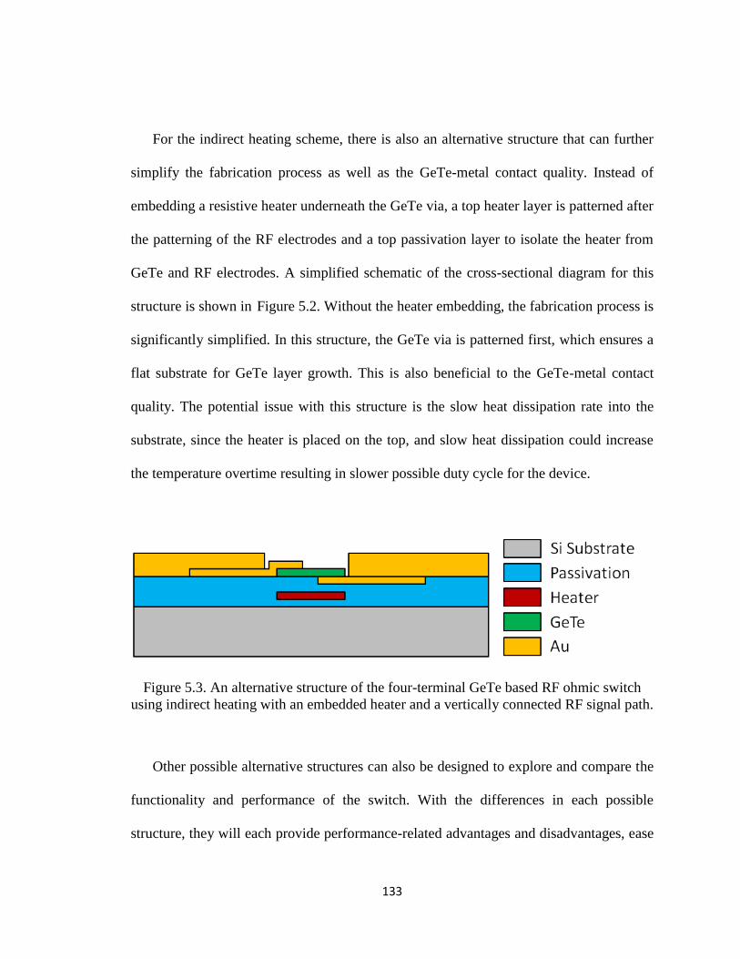
133
For the indirect heating scheme, there is also an alternative structure that can further
simplify the fabrication process as well as the GeTe-metal contact quality. Instead of
embedding a resistive heater underneath the GeTe via, a top heater layer is patterned after
the patterning of the RF electrodes and a top passivation layer to isolate the heater from
GeTe and RF electrodes. A simplified schematic of the cross-sectional diagram for this
structure is shown in Figure 5.2. Without the heater embedding, the fabrication process is
significantly simplified. In this structure, the GeTe via is patterned first, which ensures a
flat substrate for GeTe layer growth. This is also beneficial to the GeTe-metal contact
quality. The potential issue with this structure is the slow heat dissipation rate into the
substrate, since the heater is placed on the top, and slow heat dissipation could increase
the temperature overtime resulting in slower possible duty cycle for the device.
Figure 5.3. An alternative structure of the four-terminal GeTe based RF ohmic switch
using indirect heating with an embedded heater and a vertically connected RF signal path.
Other possible alternative structures can also be designed to explore and compare the
functionality and performance of the switch. With the differences in each possible
structure, they will each provide performance-related advantages and disadvantages, ease
134
of fabrication process, etc. Another example of a structural variation is shown in Figure
5.3, where a resistive heater is embedded underneath the GeTe via for indirect heating,
but the RF terminals are connected through the GeTe via vertically, which provides more
degrees of freedom when optimizing the switch performance. But the GeTe-metal contact
configuration and layer stack requires more accurate photo-lithography in the fabrication
process. Other than the ohmic switch configuration, a capacitive shunt switch
configuration can also be built with GeTe phase change material. A proposed structure of
a GeTe RF shunt switch has been reported, where the GeTe via is used to connect the
shunt path between the transmission lines [97]. In this design the switch is turned ON
when the GeTe is in the amorphous state, and the RF terminals are connected through the
conductive transmission line, providing very low insertion loss. When the GeTe is
crystallized, the switch is turned OFF at high frequencies due to the shunt element. A
good isolation has also been verified at the OFF state of the switch.
5.2.2.2. Fabrication Process Improvements
While the exploration of structural variations can help with improvement of the
functionality and performance of GeTe RF switches, efforts can also be made to improve
the effectiveness of phase transitions of the GeTe via. A lot of fabrication process related
characterizations can be done to obtain GeTe films with higher quality, better phase
transition reliability and better GeTe-metal contact stability.
In this work, the development process of GeTe RF switches has been using Ge50Te50,
due to its low crystalline state electrical resistivity and high amorphous-crystalline
135
resistivity ratio. The low crystallization temperature of Ge50Te50 compared to GeTe films
with other stoichiometric ratios as suggested in Figure 2.8 also provides the advantage of
low phase transition power. However, it is possible to explore GeTe films with composite
ratios close to 50:50 and observe the trend of resistivity and phase transition temperature
change, in order to optimize the phase transition characteristics of GeTe films [35]. This
can be realized by co-sputtering from a Ge and a Te target, or multiple GeTe targets with
different ratios.
In the film preparation process of GeTe or chalcogenide phase change materials,
works have been reported to manipulate the phase transition temperature, phase transition
speed, reliability, etc., through the introduction of doping elements, or impurity and
defects into the phase change material films [98, 99, 100]. In [99], Co has been used as
dopant to identify vacancies in crystalline GeTe, and the Co-doped GeTe films with
different Co concentrations are showing different response in the X-ray diffraction and
photoelectron spectroscopy measurements, indicating different crystalline structures. This
is primarily because the Ge vacancies in the rock-salt structure GeTe are replaced with
Co where Co-Te bonds are formed. The work in [100] has reported an ultralow-power
switching mechanism of GeTe phase change material through defect engineering. By
properly introducing defects in the crystalline GeTe, the carrier-lattice coupling can be
enhanced and therefore the required work to introduce bond distortions necessary for
amorphization is significantly reduced. This has eventually allowed reduction of required
current density of at least 80 times in order to amorphize the GeTe film compared to
sample without the introduction of defects. Similar approaches to the reported works

136
above can be explored to manually modify the phase transition characteristics in order to
obtain GeTe phase change material films with better phase transition power efficiency,
better crystalline films with higher grain size and other properties that will better suit
reconfigurable RF applications.
The GeTe-metal contact is also important to the performance of the GeTe RF
switches. Ideally, the electrical contact between the GeTe film and RF metal is required
to have minimal contact resistance, in order to achieve low insertion loss when the GeTe
is in crystalline state. Since Au is the RF electrode material used in this work and many
other similar works [93] [95], it is important to ensure good contact by implementing the
proper contact layer stack between the GeTe-Au interface. In theory, the preferred
contact material depends on the carrier type of GeTe. In our case the GeTe film is
measured to be high carrier density p-type, and therefore a metal layer with high work
function is better in order to form an ohmic contact. However, a lot of fabrication related
detail including chemical selection, surface treatment condition, contact layer structure,
etc. can affect the contact quality and phase transition process of GeTe [101]. Further
exploration can be performed to optimize the GeTe-metal contact in order to achieve
lower contact loss and more reliable switching activities.

137
BIBLIOGRAPHY
138
[1] A. Gopinath and J. B. Rankin, "GaAs FET RF Switches," IEEE Transactions on
Electron Devices, vol. 32, no. 7, pp. 1272-1278, 1985.
[2] R. H. Caverly, "Distortion in Off-State Arsenide MESFET Switches," IEEE
Transactions on Microwave Theory and Techniques, vol. 41, no. 8, pp. 1323-1328,
1993.
[3] K. W. Kobayashi, A. K. Oki, D. K. Umemoto, S. K. Z. Claxton and D. C. Streit,
"Monolithic GaAs HBT p-i-n Diode Variable Gain Amplifiers, Attenuators, and
Switches," IEEE Transactions on Microwave Theory and Techniques, vol. 41, no.
12, pp. 2295-2302, 1993.
[4] W. Arden, M. Brillouet, P. Cogez, M. Graef, B. Huizing and R. Mahnkopf, "More-
than-Moore White Paper," 2010. [Online]. Available:
http://www.itrs2.net/uploads/4/9/7/7/49775221/irc-itrs-mtm-v2_3.pdf. [Accessed 9
3 2017].
[5] B. Razavi, "Challenges in Portable RF Transciver Design," IEEE Circuits and
Devices Magazine, vol. 12, no. 5, pp. 12-25, 1995.
[6] C. A. Liechti, "Microwave Field-Effect Transistors," IEEE Transactions on
Microwave Theory and Techniques, vol. 24, no. 6, pp. 279-300, 1976.
[7] J. Goel and H. J. Wolkstein, "A 4-8 GHz Dual Gate M.E.S.F.E.T. Amplifier,"
Electronic Letters , vol. 14, no. 6, pp. 167-168, 1978.
[8] R. V. Garver, "Microwave Semiconductor Control Devices," IEEE Transactions
on microwave Theory and Techniques, vol. 27, no. 5, pp. 523-529, 1979.
[9] K. Miyatsuji and D. Ueda, "A GaAs High Power RF Single Pole Dual Throw
Switch IC for Digital Mobile Communication System," IEEE Journal of Solid-
State Circuits, vol. 30, no. 9, pp. 979-983, 1995.
[10] K. W. Kobayashi, L. Tran, A. K. Oki and D. C. Streit, "A 50 MHz-30 GHz
Broadband CO-Planar Waveguide SPDT PIN Diode Switch with 45-dB Isolation,"
IEEE Microwave and Guided Wave Letters, vol. 5, no. 2, pp. 56-58, 1995.
[11] D. Kelly, C. Brindle, C. Kemerling and M. Stuber, "The State-of-the-Art of
Silicon-on-Sapphire CMOS RF Switches," in IEEE Compound Semiconductor
Integrated Circuit Symposium, 2005.
139
[12] A. Botula, A. Joseph, J. Slinkman, R. Wolf, Z. X. He, D. Ioannou, L. Wagner, M.
Gordon, M. Abou-Khalil, R. Phelps, M. Gautsch, W. Abadeer, D. Harmon, M.
Levy, J. Benoit and J. Dunn, "A Thin-film SOI 180nm CMOS RF Switch
Technology," in IEEE Topical Meeting on Silicon Monolithic Integrated Circuits
in RF Systems, 2009.
[13] A. Tombak, "Silicon-on-Insulator (SOI) Switches for Cellular and WLAN Front-
End Applications," IEEE Radio Frequency Integrated Circuit Symposium
Workshop, 2012.
[14] T. Y. Lee and S. Lee, "Modeling of SOI FET for RF Switch Applications," in
IEEE Radio Frequency Integrated Circuits Symposium, 2010.
[15] K. E. Petersen, "Micromechanical Membrane Switches on Silicon," IBM Journal
of Research and Development, vol. 23, no. 4, pp. 376-385, 1979.
[16] J. J. Yao and M. F. Chang, "A surface micromachined miniature switch for
telecommunications applications with signal frequencies from DC up to 4 GHz,"
in International Conference on Solid-State Sensors and Actuators, 1995.
[17] C. Goldsmith, T. H. Lin, B. Powers, W. R. Wu and B. Norvell, "Micromechanical
Membrane Switches for Microwave Applications," in IEEE MTT-S International
Microwave Symposium, 1995.
[18] S. P. Pacheco, L. P. B. Katehi and C. T. C. Nguyen, "Design of Low Actuation
Voltage RF MEMS Switch," in IEEE MTT-S International Microwave Symposium
Digest, 2000.
[19] C. L. Goldsmith, Z. Yao, S. Eshelman and D. Denniston, "Performance of Low-
Loss RF MEMS Capacitive Switches," IEEE Microwave and Guided Wave
Letters, vol. 8, no. 8, pp. 269-271, 1998.
[20] G. M. Rebeiz and J. B. Muldavin, "RF MEMS switches and switch circuits," IEEE
Microwave Magazine, vol. 2, no. 4, pp. 59-71, 2001.
[21] S. Raoux, C. T. Rettner, Y.-C. Chen, J. Jordan-Sweet, Y. Zhang, M. Caldwell, H. -
S. P. Wong, D. Milliron and J. Cha, "Scaling Properties of Phase Change
Materials," in Non-Volatile Memory Technology Symposium, Albuquerque, NM,
2007.
[22] S. Raoux, H.-Y. Cheng, B. Munoz and J. Jordan-Sweet, "Crystallization
characteristics of Ge-Sb and Ge-Te phase change materials," in Eur Phase Change

140
Ovonic Science Symposium, 2009.
[23] S. R. Ovshinsky, "Reversible electrical switching phenomena in disordered
structures," Physical Review Letters, vol. 21, no. 20, pp. 1450-1453, 1968.
[24] N. Yamada, E. Ohno, K. Nishiuchi and N. Akahira, "Rapid‐phase transitions of
GeTe‐Sb2Te3 pseudobinary amorphous thin films for an optical disk memory,"
Journal of Applied Physics, vol. 69, no. 5, pp. 2849-2856, 1991.
[25] A. Pirovano, A. L. Lacaita, A. Benvenuti, F. Pellizzer and R. Bez, "Electronic
Switching in Phase-Change Memories," IEEE Transactions on Electron Devices,
vol. 51, no. 3, pp. 452-459, 2004.
[26] J. Feinleib, J. deNeufville, S. C. Moss and S. R. Ovshinsky, "Rapid reversible
light‐induced crystallization of amorphous semiconductors," Applied Physics
Letters, vol. 18, no. 6, pp. 254-257, 1971.
[27] T. Takamori, R. Roy and G. J. McCarthy, "Observations of Surface‐Nucleated
Crystallization in Memory‐Switching Glasses," Journal of Applied Physics, vol.
42, no. 6, pp. 2577-2578, 1971.
[28] J. H. Coombs, A. P. J. M. Jongenelis, W. VanEs-Spiekman and B. A. J. Jacobs,
"Laser‐induced crystallization phenomena in GeTe‐based alloys. I.
Characterization of nucleation and growth," Journal of Applied Physics, vol. 78,
no. 8, pp. 4906-4917, 1995.
[29] J. H. Coombs, A. P. J. M. Jongenelis, W. VanEs-Spiekman and B. A. J. Jacobs,
"Laser‐induced crystallization phenomena in GeTe‐based alloys. II. Composition
dependence of nucleation and growth," Journal of Applied Physics, vol. 78, no. 8,
pp. 4918-4928, 1995.
[30] A. P. J. M. Jongenelis, J. H. Commbs, W. VanEs-Spiekman and B. A. J. Jacobs,
"Laser‐induced crystallization phenomena in GeTe‐based alloys. III. GeTeSe
alloys for a CD compatible erasable disk," Journal of Applied Physics, vol. 79, no.
11, pp. 8349-8356, 1996.
[31] B. Hyot, X. Biquard and L. Poupinet, "Local structures of morphous and
crystalline GeTe and GeSbTe," Proceedings of EPCOS, 2003.
[32] S. Raoux, B. Munoz, H.-Y. Cheng and J. L. Jordan-Sweet, "Phase transitions in
Ge–Te phase change materials studied by time-resolved x-ray diffraction," Applied
Physics Letters, 2009.

141
[33] A. H. Edwards, A. C. Pineda, P. A. Schultz, M. G. Martin, A. P. Thompson, H. P.
Hjalmarson and C. J. Umrigar, "Electronic structure of intrinsic defects in
crystalline germanium telluride," Physical Review B, vol. 73, no. 4, p. 045210,
2006.
[34] S. Raoux, H. -Y. Cheng, M. A. Caldwell and H.-S. P. Wong, "Crystallization times
of Ge–Te phase change materials as a function of composition," Applied Physics
Letters, 2009.
[35] M. Chen, K. A. Rubin and R. W. Barton, "Compound materials for reversible,
phase‐change optical data storage," Applied Physics Letters, vol. 49, no. 9, pp.
502-504, 1986.
[36] K. N. Chen, L. Krusin-Elbaum, D. M. Newns, B. G. Elmegreen, R. Cheek, N.
Rana, A. M. Young, S. J. Koester and C. Lam, "Programmable via Using
Indirectly Heated Phase-Change Switch for Reconfigurable Logic Applications,"
IEEE Electron Device Letters, vol. 21, no. 1, pp. 131-133, 2008.
[37] M. Takenaga, N. Yamada, S. Ohara, K. Nishiuchi, M. Nagashima, T. Kashihara, S.
Nakamura and T. Yamashita, "New optical erasable medium using tellurium
suboxide thin film," Proceedings of SPIE, vol. 420, pp. 173-177, 1983.
[38] N. Yamada, M. Takao and M. Takenaga, "Te-Ge-Sn-Au Phase change recording
film for optical disk," Proceedings of SPIE, vol. 695, pp. 79-85, 1986.
[39] M. Terao, T. Nishida, Y. Miyauchi, S. Horigome, T. Kaku and N. Ohta, "In-Se
Based Phase Change Reversible Optical Recording Film," Proceedings of SPIE,
vol. 695, pp. 105-109, 1986.
[40] J. C. Rhee, M. Okuda and T. Matsushita, "Write-Erase Characteristics of Phase
Change Optical Recording in Ga–Se–Te Systems," Japanese Journal of Applied
Physics, vol. 26, no. 1, pp. 102-105, 1987.
[41] N. Yamada, E. Ohno, N. Akahira, K. Nishiuchi, K. Nagata and M. Takao, "High
Speed Overwritable Phase Change Optical Disk Material," Japanese Journal of
Applied Physics, vol. 26, no. S4, pp. 61-66, 1987.
[42] K. Nishimura, M. Suzuki, I. Morimoto and K. Mori, "Ge–Te–Sb Based
Overwritable Phase Change Optical Disk," Japanese Journal of Applied Physics,
vol. 28, no. S3, pp. 135-139, 1989.
[43] H. Iwasaki, Y. Ide, M. Harigaya, Y. Kageyama and I. Fujimura, "Completely
Erasable Phase Change Optical Disk," Japanese Journal of Applied Physics, vol.
142
31, no. S2, pp. 461-465, 1992.
[44] K. A. Rubin and M. Chen, "Progress and issues of phase-change erasable optical
recording media," Thin Solid Films, vol. 1, no. 2, pp. 129-139, 1989.
[45] G. Wicker, "Nonvolatile, High Density, High Performance Phase Change
Memory," in Asia Pacific Symposium on Microelectronics and MEMS, 1999.
[46] J. Hegedus and S. R. Elliott, "Microscopic origin of the fast crystallization ability
of Ge–Sb–Te phase-change memory materials," Nature Materials, vol. 7, no. 5,
pp. 399-405, 2008.
[47] D. Ielmini and Y. Zhang, "Analytical model for subthreshold conduction and
threshold switching in chalcogenide-based memory devices," Journal of Applied
Physics, vol. 102, no. 5, p. 054517, 2007.
[48] S. Lai, "Current status of the phase change memory and its future," in IEEE
International Electron Devices Meeting, 2003.
[49] B. Yu, X. Sun, S. Ju, D. B. Janes and M. Meyyappan, "Chalcogenide-Nanowire-
Based Phase Change Memory," IEEE Transactions on Nanotechnology, vol. 7, no.
4, pp. 496-502, 2008.
[50] M. K. Qureshi, V. Srinivasan and J. A. Rivers, "Scalable High Performance Main
Memory System Using Phase-Change Memory Technology," ACM SIGARCH
Computer Architecture News, vol. 37, no. 3, pp. 24-33, 2009.
[51] H.-S. P. Wong, S. Raoux, S. Kim, J. Liang, J. P. Reifenberg, B. Rajendran, M.
Asheghi and K. E. Goodson, "Phase Change Memory," Proceedings of the IEEE,
vol. 98, no. 12, pp. 2201-2227, 2010.
[52] H. Lo, E. Chua, J. C. Huang, C. C. Tan, C.-Y. Wen, R. Zhao, L. Shi, C. T. Chong,
J. Paramesh, T. E. Schlesinger and J. A. Bain, "Three-Terminal Probe
Reconfigurable Phase-Change Material Switches," IEEE Transactions on Electron
Devices, vol. 57, no. 1, pp. 312-320, 2010.
[53] E. K. Chua, L. P. Shi, R. Zhao, K. G. Lim, T. C. Chong, T. E. Schlesinger and J.
A. Bain, "Low resistance, high dynamic range reconfigurable phase change switch
for radio frequency applications," Applied Physics Letters, vol. 97, no. 18, p.
183506, 2010.
[54] K. L. Chopra and S. K. Bahl, "Amorphous versus Crystalline GeTe Films. I.
Growth and Structural Behavior," Journal of Applied Physics, vol. 40, no. 10, pp.
143
4171-4178, 1969.
[55] S. K. Bahl and K. L. Chopra, "Amorphous versus Crystalline GeTe Films. III.
Electrical Properties and Band Structure," Journal of Applied Physics, vol. 41, no.
5, pp. 2196-2212, 1970.
[56] S. K. Bahl and K. L. Chopra, "Amorphous Versus Crystalline GeTe Films. II.
Optical Properties," Journal of Applied Physics, vol. 40, no. 12, pp. 4940-4947,
1969.
[57] M. Jafari and M. Rais-Zadeh, "Zero-static-power phase-change optical modulator,"
Optics Letters, vol. 41, no. 6, pp. 1177-1180, 2016.
[58] M. Jafari and M. Rais-Zadeh, "A 1550 nm Phase Change Electro-Optical Shutter,"
in IEEE 29th International Conference on Micro Electro Mechanical Systems,
2016.
[59] T. Okabe and M. Nakagawa, "Crystallization Behavior and Local Order of
Amorphous GexTe1− x Films," Journal of Non-Crystalline Solids, vol. 88, no. 2-
3, pp. 182-195, 1986.
[60] M. R. King, B. P. Wagner, E. B. Jones, N. El-Hinnawy, P. Boroduiln, S. R.
McLaughlin, J. S. Mason, R. S. Howell, M. J. Lee and R. M. Young,
"Development of cap-free sputtered GeTe films for inline phase change switch
based RF circuits," Journal of Vacuum Science & Technology B, vol. 32, no. 4, p.
041204, 2014.
[61] Y. Shim, G. Hummel and M. Rais-Zadeh, "RF switches using phase change
materials," in IEEE 26th International Conference on Micro Electro Mechanical
Systems (MEMS), Taipei, 2013.
[62] N. El-Hinnawy, P. Borodulin, B. Wagner, M. R. King, J. S. Mason, E. B. Jones, S.
McLaughlin, V. Veliadis, M. Snook, M. E. Sherwin, R. S. Howell, R. M. Young
and M. J. Lee, "A Four-Terminal, Inline, Chalcogenide Phase-Change RF Switch
Using an Independent Resistive Heater for Thermal Actuation," IEEE Electron
Device Letters, vol. 34, no. 10, pp. 13131-1315, 2013.
[63] N. El-Hinnawy, P. Borodulin, B. P. Wagner, M. R. King, J. S. Mason, E. B. Jones,
V. Veliadis, R. S. Howell, R. M. Young and M. J. Lee, "A 7.3 THz Cut-Off
Frequency, Inline, Chalcogenide Phase-Change RF Switch Using an Independent
Resistive Heater for Thermal Actuation," in IEEE Compound Semiconductor
Integrated Circuit Symposium, 2013.
144
[64] M. Wang, Y. Shim and M. Rais-Zadeh, "A Low-Loss Directly Heated Two-Port
RF Phase Change Switch," IEEE Electron Device Letters, vol. 35, no. 4, pp. 491-
493, 2014.
[65] M. Wang and M. Rais-Zadeh, "Directly Heated Four-Terminal Phase Change
Switches," in IEEE MTT-S International Microwave Symposium, Tampa, FL,
2014.
[66] M. Rais-Zadeh, Y. Shim and M. Wang, "Directly heated RF phase change switch".
US Patent US9419213 B2, 5 June 2014.
[67] R. F. Bunshah, Deposition Technologies for Films and Coatings: Developments
and Applications, Park Ridge, NJ: Noyes Publications, 1982.
[68] K. Nakamura, K. Inagawa, K. Tsuruoka and S. Komiya, "Applications of Wear-
Resistant Thick Films Formed by Physical Vapor Deposition Processes," Thin
Solid Films, vol. 40, pp. 155-167, 1977.
[69] J. Moon, H. Seo and D. Le, "Development toward High-power Sub-1-ohm DC-67
GHz RF Switches using Phase Change Materials for Reconfigurable RF Front-
end," in IEEE MTT-S International Microwave Symposium, 2014.
[70] N. El-Hinnawy, P. Borodulin, E. B. Jones, B. P. Wagner, M. R. King, J. S. Mason,
J. Hartman, R. S. Howell, M. J. Lee and R. M. Young, "Improvements in GeTe-
Based Inline Phase-Change Switch Technology for RF Switching Applications," in
CS MANTECH Conference, 2014.
[71] T. B. Jackson, A. V. Virkar, K. L. More, R. B. Dinwiddie and R. A. Cutler, "High-
Thermal-Conductivity Aluminum Nitride Ceramics: The Effect of
Thermodynamic, Kinetic, and Microstructural Factors," Journal of the American
Ceramic Society, vol. 80, no. 6, pp. 1421-1435, 1997.
[72] M. Wang, F. Lin and M. Rais-Zadeh, "Performance Measurements and Non-
Linearity Modeling of GeTe Phase Change RF Switches with Direct and Indirect
Heating Schemes," in 2015 IEEE MTT-S International Microwave Symposium,
Phoenix, AZ, 2015.
[73] Y. Shim, G. Hummel and M. Rais-Zadeh, "Non-Linearity Analysis of RF Ohmic
Switches Based on Phase Change Materials," IEEE Electron Device Letters, vol.
35, no. 3, pp. 405-407, 2014.
[74] Y. S. Ju, K. Kurabayashi and K. E. Goodson, "Thermal Characterization of IC
Passivation Layers Using Joule Heating and Optical Thermometry," Microscale

145
Thermophysical Engineering, vol. 2, no. 2, pp. 101-110, 1998.
[75] M. Wang and M. Rais-Zadeh, "Development and evaluation of germanium
telluride phase change material based ohmic switches for RF applications,"
Journal of Micromechanics and Microengineering, vol. 27, no. 1, p. 013001, 2016.
[76] N. El-Hinnawy, P. Borodulin, M. Torpey, F. Kuss, A. Ezis, J. Paramesh, J. Bain,
T. E. Schlesinger, R. S. Howell, M. J. Lee, D. Nichols and R. M. Young,
"Reconfigurable Inline Phase-Change Switches for Broadband Applications," in
IEEE MTT-S International Microwave Symposium, 2015.
[77] R. Wolf, A. Joseph, A. Botula and J. Slinkman, "A Thin-film SOI 180nm CMOS
RF Switch," in IEEE Topical Meeting on Silicon Monolithic Integrated Circuits in
RF Systems, 2009.
[78] S. Makioka, Y. Anda, K. Miyatsuji and D. Ueda, "Super Self-Aligned GaAs RF
Switch IC with 0.25 dB Extremely Low Insertion Loss for Mobile Communication
Systems," IEEE Transactions on Electron Devices, vol. 48, no. 8, pp. 1510-1514,
2001.
[79] M. Wang, F. Lin and M. Rais-Zadeh, "An X-Band Reconfigurable Bandpass Filter
Using Phase Change RF Switches," in IEEE 16th Topical Meeting on Silicon
Monolithic Integrated Circuits in RF Systems, Austin, TX, 2016.
[80] Y. Shim, Z. Wu and M. Rais-Zadeh, "A High-Performance Continuously Tunable
MEMS Bandpass Filter at 1 GHz," IEEE Transactions on Microwave Theory and
Techniques, vol. 60, no. 8, pp. 2439-2447, 2012.
[81] S. Lucyszyn, "Review of radio frequency microelectromechanical systems
technology," IEE Proceedings-Science, Measurement and Technology, vol. 151,
no. 2, pp. 93-103, 2004.
[82] A. R. Brown and G. M. Rebeiz, "A Varactor-Tuned RF Filter," IEEE Transactions
on Microwave Theory and Techniques, vol. 48, no. 7, pp. 1157-1160, 2000.
[83] A. Pothier, J. -C. Orlianges, G. Zheng, C. Champeaux, A. Catherinot, D. Cros, P.
Blondy and J. Papapolymerou, "Low-loss 2-bit tunable bandpass filters using
MEMS DC contact switches," IEEE Transactions on Microwave Theory and
Techniques, vol. 53, no. 1, pp. 354-360, 2005.
[84] P. S. Carter, "Magnetically-Tunable Microwave Filters Using Single-Crystal
Yttrium-Iron-Garnet Resonators," IRE Transactions on Microwave Theory and
146
Techniques, vol. 9, no. 3, pp. 252-260, 1961.
[85] Y. Zhu, G. Qiu, K. H. Chi, B. B. T. Wang and C. S. Tsai, "A Tunable X-Band
Band-Pass Filter Module Using YIG/GGG Layer on RT/Duroid Substrate," IEEE
Transactions on Magnetics, vol. 45, no. 10, pp. 4195-4198, 2009.
[86] S. Courreges, Y. Li, Z. Zhao, K. Choi, A. Hunt and J. Papapolymerou, "Two-Pole
X -Band-Tunable Ferroelectric Filters With Tunable Center Frequency, Fractional
Bandwidth, and Return Loss," IEEE Transactions on Microwave Theory and
Techniques, vol. 57, no. 12, pp. 2872-2881, 2009.
[87] D. Bouyge, A. Crunteanu, J. -C. Orlianges, D. Passerieux, C. Champeaux, A.
Catherinot, A. Velez, J. Bonache, F. Martin and P. Blondy, "Reconfigurable
Bandpass Filter Based on Split Ring Resonators and Vanadium Dioxide (VO2)
Microwave Switches," in 2009 Asia Pacific Microwave Conference, Singapore,
2009.
[88] R. Singh, G. Slovin, M. Xu, A. Khairi, S. Kundu, T. E. Schlesinger, J. A. Bain and
J. Paramesh, "A 3/5 GHz Reconfigurable CMOS Low-Noise Amplifier Integrated
with a Four-Terminal Phase-Change RF Switch," in IEEE International Electron
Devices Meeting, 2015.
[89] G. Hummel, Y. Hui and M. Rinaldi, "Reconfigurable Mode of Vibration in AlN
MEMS Resonators Using Phase Change Materials," in IEEE International
Ultrasonics Symposium, 2014.
[90] M. Wang, L. Feng and M. Rais-Zadeh, "Need a Change? Try GeTe: A
Reconfigurable Filter Using Germanium Telluride Phase Change RF Switches,"
IEEE Microwave Magazine, vol. 17, no. 12, pp. 70-79, 2016.
[91] S. Park and G. M. Rebeiz, "Low-Loss Two-Pole Tunable Filters With Three
Different Predefined Bandwidth Characteristics," IEEE Transactions on
Microwave Theory and Techniques, vol. 56, no. 5, pp. 1137-1148, 2008.
[92] G. L. Matthaei, L. Young and E. M. T. Jones, Microwave Filters, Impedance
Matching Networks and Coupling Structures, Norwood, MA: Artech House, 1980.
[93] N. El-Hinnawy, P. Borodulin, B. P. Wagner, M. R. King, E. B. Jones, R. S.
Howell, M. J. Lee and R. M. Young, "Low-loss latching microwave switch using
thermally pulsed non-volatile chalcogenide phase change materials," Applied
Physics Letters, vol. 105, no. 1, p. 013501, 2014.
147
[94] E. K. Chua, "Development of Phase Change Switches with Low Resistance in the
“ON state”," Diss. Carnegie Mellon University, Pittsburgh, PA, 2011.
[95] J. S. Moon, H. C. Seo, D. Le, H. Fung, A. Schmitz, T. Oh, S. Kim, K. A. Son, D.
Zehnder and B. Yang, "11 THz Figure-of-Merit Phase-change RF Switches for
Reconfigurable Wireless Front-ends," in IEEE MTT-S International Microwave
Symposium, 2015.
[96] N. El-Hinnawy, P. Borodulin, E. B. Jones, B. P. Wagner, M. R. King, J. S. Mason,
J. Bain, J. Paramesh, T. E. Schlesinger, R. S. Howell, M. J. Lee and R. M. Young,
"12.5 THz Fco GeTe Inline Phase-Change Switch Technology for Reconfigurable
RF and Switching Applications," in IEEE Compound Semiconductor Integrated
Circuit Symposium, 2014.
[97] J. S. Moon, H. C. Seo and D. Le, "Development toward High-power Sub-1-ohm
DC-67 GHz RF Switches using Phase Change Materials for Reconfigurable RF
Front-end," in IEEE MTT-S International Microwave Symposium, 2014.
[98] A. Fantini, V. Sousa, L. Perniola, E. Gourvest, J. C. Bastien, S. Maitrejean, S.
Braga, N. Pashkov, A. Bastard, B. Hyot, A. Roule, A. Persico, H. Feldis, C. Jahan,
J. F. Nodin, D. Blachier, A. Toffoli, G. Reimbold, F. Fillot, F. Pierre, R.
Annunziata, D. Benshael, P. Mazoyer, C. Vallee, T. Billon, J. Hazart, B. De Salvo
and F. Boulanger, "N-doped GeTe as Performance Booster for Embedded Phase-
Change Memories," in IEEE International Electron Devices Meeting, 2010.
[99] F. Tong, X. S. Miao, Y. Wu, Z. P. Chen, H. Tong and X. M. Cheng, "Effective
method to identify the vacancies in crystalline GeTe," Applied Physics Letters, vol.
97, no. 26, p. 261904, 2010.
[100] P. Nukala, C.-C. Lin, R. Composto and R. Agarwal, "Ultralow-power switching
via defect engineering in germanium telluride phase-change memory devices,"
Nature Communications, vol. 7, 2016.
[101] H. M. Aldosari, H. Simchi, Z. Ding, K. A. Cooley, S. Y. Yu and S. E. Mohney,
"Impact of Premetallization Surface Preparation on Nickel-based Ohmic Contacts
to Germanium Telluride: An X-ray Photoelectron Spectroscopic Study," ACS
Applied Materials & Interfaces, vol. 8, no. 50, pp. 34802-34809, 2016.