Embed Size (px)
Citation preview

Cover
PG-FP5 V2.17 Flash Memory Programmer
User’s Manual : Common
Rev.5.00 Mar 2019
All information contained in these materials, including products and product specifications, represents information on the product at the time of publication and is subject to change by Renesas Electronics Corporation without notice. Please review the latest information published by Renesas Electronics Corporation through various means, including the Renesas Electronics Corporation website (http://www.renesas.com).
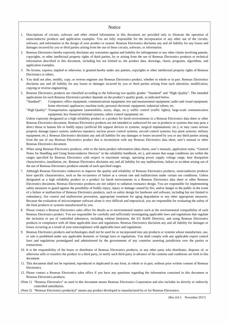
Notice 1. Descriptions of circuits, software and other related information in this document are provided only to illustrate the operation of
semiconductor products and application examples. You are fully responsible for the incorporation or any other use of the circuits, software, and information in the design of your product or system. Renesas Electronics disclaims any and all liability for any losses and damages incurred by you or third parties arising from the use of these circuits, software, or information.
2. Renesas Electronics hereby expressly disclaims any warranties against and liability for infringement or any other claims involving patents, copyrights, or other intellectual property rights of third parties, by or arising from the use of Renesas Electronics products or technical information described in this document, including but not limited to, the product data, drawings, charts, programs, algorithms, and application examples.
3. No license, express, implied or otherwise, is granted hereby under any patents, copyrights or other intellectual property rights of Renesas Electronics or others.
4. You shall not alter, modify, copy, or reverse engineer any Renesas Electronics product, whether in whole or in part. Renesas Electronics disclaims any and all liability for any losses or damages incurred by you or third parties arising from such alteration, modification, copying or reverse engineering.
5. Renesas Electronics products are classified according to the following two quality grades: “Standard” and “High Quality”. The intended applications for each Renesas Electronics product depends on the product’s quality grade, as indicated below. “Standard”: Computers; office equipment; communications equipment; test and measurement equipment; audio and visual equipment;
home electronic appliances; machine tools; personal electronic equipment; industrial robots; etc. “High Quality”: Transportation equipment (automobiles, trains, ships, etc.); traffic control (traffic lights); large-scale communication
equipment; key financial terminal systems; safety control equipment; etc. Unless expressly designated as a high reliability product or a product for harsh environments in a Renesas Electronics data sheet or other Renesas Electronics document, Renesas Electronics products are not intended or authorized for use in products or systems that may pose a direct threat to human life or bodily injury (artificial life support devices or systems; surgical implantations; etc.), or may cause serious property damage (space system; undersea repeaters; nuclear power control systems; aircraft control systems; key plant systems; military equipment; etc.). Renesas Electronics disclaims any and all liability for any damages or losses incurred by you or any third parties arising from the use of any Renesas Electronics product that is inconsistent with any Renesas Electronics data sheet, user’s manual or other Renesas Electronics document.
6. When using Renesas Electronics products, refer to the latest product information (data sheets, user’s manuals, application notes, “General Notes for Handling and Using Semiconductor Devices” in the reliability handbook, etc.), and ensure that usage conditions are within the ranges specified by Renesas Electronics with respect to maximum ratings, operating power supply voltage range, heat dissipation characteristics, installation, etc. Renesas Electronics disclaims any and all liability for any malfunctions, failure or accident arising out of the use of Renesas Electronics products outside of such specified ranges.
7. Although Renesas Electronics endeavors to improve the quality and reliability of Renesas Electronics products, semiconductor products have specific characteristics, such as the occurrence of failure at a certain rate and malfunctions under certain use conditions. Unless designated as a high reliability product or a product for harsh environments in a Renesas Electronics data sheet or other Renesas Electronics document, Renesas Electronics products are not subject to radiation resistance design. You are responsible for implementing safety measures to guard against the possibility of bodily injury, injury or damage caused by fire, and/or danger to the public in the event of a failure or malfunction of Renesas Electronics products, such as safety design for hardware and software, including but not limited to redundancy, fire control and malfunction prevention, appropriate treatment for aging degradation or any other appropriate measures. Because the evaluation of microcomputer software alone is very difficult and impractical, you are responsible for evaluating the safety of the final products or systems manufactured by you.
8. Please contact a Renesas Electronics sales office for details as to environmental matters such as the environmental compatibility of each Renesas Electronics product. You are responsible for carefully and sufficiently investigating applicable laws and regulations that regulate the inclusion or use of controlled substances, including without limitation, the EU RoHS Directive, and using Renesas Electronics products in compliance with all these applicable laws and regulations. Renesas Electronics disclaims any and all liability for damages or losses occurring as a result of your noncompliance with applicable laws and regulations.
9. Renesas Electronics products and technologies shall not be used for or incorporated into any products or systems whose manufacture, use, or sale is prohibited under any applicable domestic or foreign laws or regulations. You shall comply with any applicable export control laws and regulations promulgated and administered by the governments of any countries asserting jurisdiction over the parties or transactions.
10. It is the responsibility of the buyer or distributor of Renesas Electronics products, or any other party who distributes, disposes of, or otherwise sells or transfers the product to a third party, to notify such third party in advance of the contents and conditions set forth in this document.
11. This document shall not be reprinted, reproduced or duplicated in any form, in whole or in part, without prior written consent of Renesas Electronics.
12. Please contact a Renesas Electronics sales office if you have any questions regarding the information contained in this document or Renesas Electronics products.
(Note 1) “Renesas Electronics” as used in this document means Renesas Electronics Corporation and also includes its directly or indirectly controlled subsidiaries.
(Note 2) “Renesas Electronics product(s)” means any product developed or manufactured by or for Renesas Electronics.
(Rev.4.0-1 November 2017)
PG-FP5 V2.17 PREFACE
R20UT2922EJ0500 Rev.5.00 Page 3 of 163 Mar 29, 2019
PREFACE Thank you for purchasing the PG-FP5 flash memory programmer. The PG-FP5 is a flash memory programmer for Renesas Electronics microcontrollers. All components of the PG-FP5 are listed under “1.4 Package Components”. If you have any questions about the PG-FP5, contact your local distributor. The manuals relevant to usage of the PG-FP5 are listed below. The manuals for your product consist of two volumes; a common part and a part for the corresponding MCUs. Be sure to read both volumes before using the PG-FP5. You can download the latest manuals from the Renesas Tools homepage (https://www.renesas.com/pg-fp5). Related manuals
Document name Document number
PG-FP5 V2.17 Flash Memory Programmer User's Manual Common This manual
PG-FP5 V2.17 Flash Memory Programmer User's Manual RL78, 78K, V850, RX100, RX200, RX61x, RX62x, RX63x, R8C, SuperH
R20UT2923E
PG-FP5 V2.17 Flash Memory Programmer User's Manual RH850, RX64x, RX65x, RX66x, RX71x
R20UT2924E
PG-FP5 V2.17 PREFACE
R20UT2922EJ0500 Rev.5.00 Page 4 of 163 Mar 29, 2019
Important Before using this product, be sure to read this user’s manual carefully. Keep this user’s manual, and refer to it when you have questions about this product. Purpose of use of the product:
This product is a device to support the development of systems that uses Renesas Electronics microcontrollers. This product is a tool that erases, writes and verifies programs on a Renesas Electronics on-chip flash memory microcontroller on the target system. Be sure to use this product correctly according to said purpose of use. Please avoid using this product other than for its intended purpose of use.
For those who use this product:
This product can only be used by those who have carefully read the user’s manual and know how to use it. Use of this product requires basic knowledge of electric circuits, logical circuits, and MCUs.
When using this product:
(1) This product is a development-support unit for use in your program development and evaluation stages. When a program you have finished developing is to be incorporated in a mass-produced product, the judgment as to whether it can be put to practical use is entirely your own responsibility, and should be based on evaluation of the device on which it is installed and other experiments.
(2) In no event shall Renesas Electronics Corporation be liable for any consequence arising from the use of this product.
(3) Renesas Electronics Corporation strives to provide workarounds for and correct trouble with products malfunctions, with some free and some incurring charges. However, this does not necessarily mean that Renesas Electronics Corporation guarantees the provision of a workaround or correction under any circumstances.
(4) This product covered by this document has been developed on the assumption that it will be used for program development and evaluation in laboratories. Therefore, it does not fall within the scope of applicability of the Electrical Appliance and Material Safety Law and protection against electromagnetic interference when used in Japan.
(5) Renesas Electronics Corporation cannot predict all possible situations and possible cases of misuse that carry a potential for danger. Therefore, the warnings in this user's manual and the warning labels attached to this product do not necessarily cover all such possible situations and cases. The customer is responsible for correctly and safely using this product.
(6) The product covered by this document has not been through the process of checking conformance with UL or other safety standards and IEC or other industry standards. This fact must be taken into account when the product is taken from Japan to some other country.
(7) Renesas Electronics Corporation will not assume responsibility of direct or indirect damage caused by an accidental failure or malfunction in this product.
When disposing of this product:
Penalties may be applicable for incorrect disposal of this waste, in accordance with your national legislation.
PG-FP5 V2.17 PREFACE
R20UT2922EJ0500 Rev.5.00 Page 5 of 163 Mar 29, 2019
Usage restrictions: This product has been developed as a means of supporting system development by users. Therefore, do not use it as an embedded device in other equipment. Also, do not use it to develop systems or equipment for use in the following fields. (1) Transportation and vehicular (2) Medical (equipment that has an involvement in human life) (3) Aerospace (4) Nuclear power control (5) Undersea repeaters If you are considering the use of this product for one of the above purposes, please be sure to consult your local distributor.
About product changes:
We are constantly making efforts to improve the design and performance of our product. Therefore, the specification or design of the product, or this user's manual, may be changed without prior notice.
About rights:
(1) We assume no responsibility for any damage or infringement on patent rights or any other rights arising from the use of any information, products or circuits presented in this user’s manual.
(2) The information or data in this user’s manual does not implicitly or otherwise grant a license to patent rights or any other rights belonging to Renesas or to a third party.
(3) This user’s manual and this product are copyrighted, with all rights reserved by Renesas. This user’s manual may not be copied, duplicated or reproduced, in whole or part, without prior written consent from Renesas.
About diagrams:
Some diagrams in this user’s manual may differ from the objects they represent.
PG-FP5 V2.17 PREFACE
R20UT2922EJ0500 Rev.5.00 Page 6 of 163 Mar 29, 2019
Precautions for Safety This chapter describes the precautions which should be taken in order to use this product safely and properly. Be sure to read and understand this chapter before using this product. Contact us if you have any questions about the precautions described here. This chapter describes the precautions which should be taken in order to use this product safely and properly. Be sure to read this chapter before using this product.
WARNING
WARNING indicates a potentially dangerous situation that will cause death or heavy wound unless it is avoided.
CAUTION
CAUTION indicates a potentially dangerous situation that will cause a slight injury or a medium-degree injury or property damage unless it is avoided.
In addition to the two above, the following are also used as appropriate.
means WARNING or CAUTION. Example:
CAUTION AGAINST AN ELECTRIC SHOCK
means PROHIBITION. Example:
DISASSEMBLY PROHIBITED
means A FORCIBLE ACTION. Example:
UNPLUG THE POWER CABLE FROM THE RECEPTACLE.
PG-FP5 V2.17 PREFACE
R20UT2922EJ0500 Rev.5.00 Page 7 of 163 Mar 29, 2019
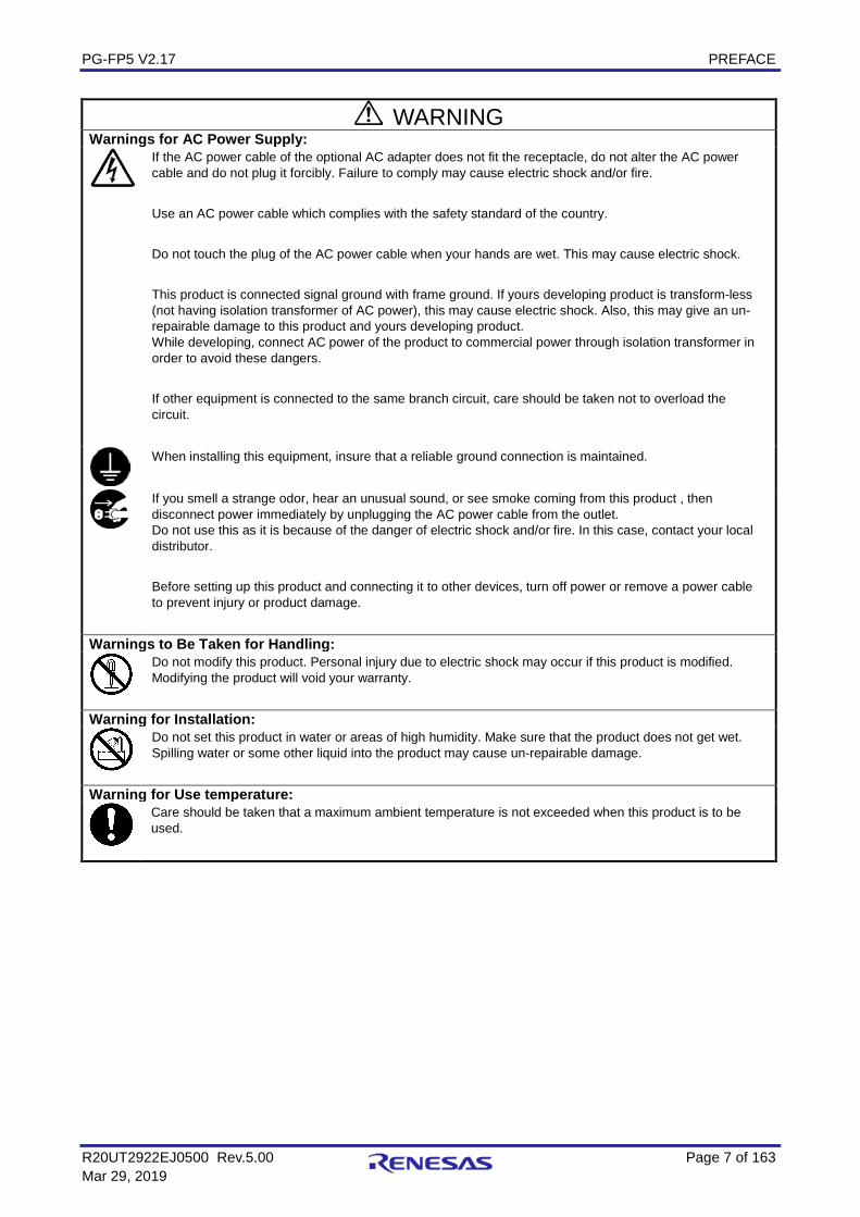
WARNING Warnings for AC Power Supply:
If the AC power cable of the optional AC adapter does not fit the receptacle, do not alter the AC power cable and do not plug it forcibly. Failure to comply may cause electric shock and/or fire. Use an AC power cable which complies with the safety standard of the country. Do not touch the plug of the AC power cable when your hands are wet. This may cause electric shock. This product is connected signal ground with frame ground. If yours developing product is transform-less (not having isolation transformer of AC power), this may cause electric shock. Also, this may give an un-repairable damage to this product and yours developing product. While developing, connect AC power of the product to commercial power through isolation transformer in order to avoid these dangers. If other equipment is connected to the same branch circuit, care should be taken not to overload the circuit.
When installing this equipment, insure that a reliable ground connection is maintained.
If you smell a strange odor, hear an unusual sound, or see smoke coming from this product , then disconnect power immediately by unplugging the AC power cable from the outlet. Do not use this as it is because of the danger of electric shock and/or fire. In this case, contact your local distributor. Before setting up this product and connecting it to other devices, turn off power or remove a power cable to prevent injury or product damage.
Warnings to Be Taken for Handling:
Do not modify this product. Personal injury due to electric shock may occur if this product is modified. Modifying the product will void your warranty.
Warning for Installation:
Do not set this product in water or areas of high humidity. Make sure that the product does not get wet. Spilling water or some other liquid into the product may cause un-repairable damage.
Warning for Use temperature:
Care should be taken that a maximum ambient temperature is not exceeded when this product is to be used.
PG-FP5 V2.17 PREFACE
R20UT2922EJ0500 Rev.5.00 Page 8 of 163 Mar 29, 2019
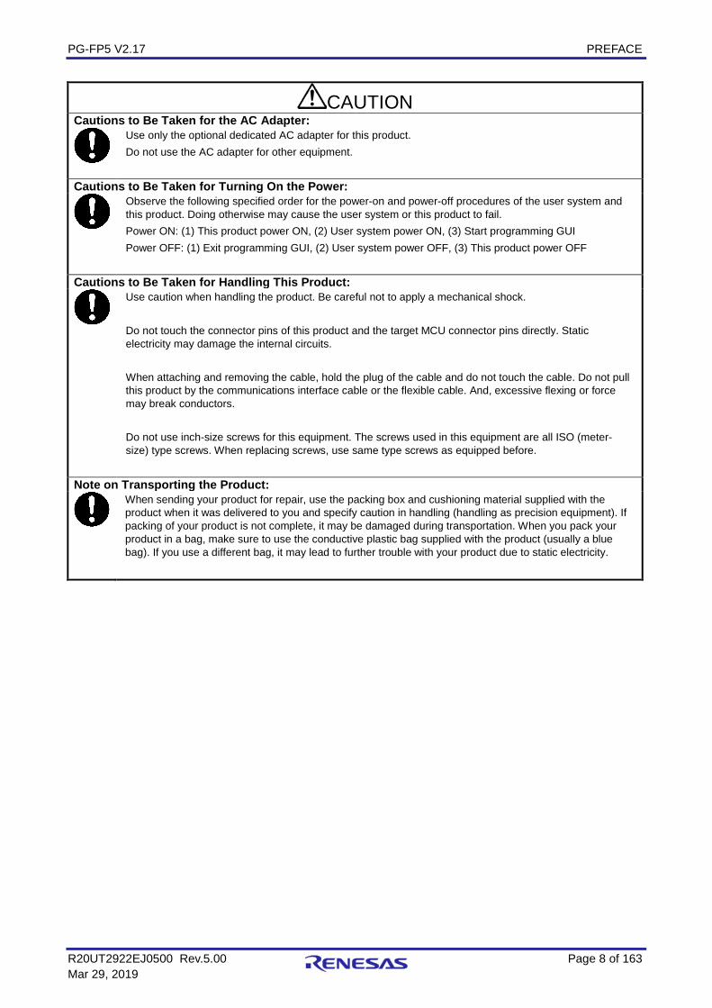
CAUTION Cautions to Be Taken for the AC Adapter:
Use only the optional dedicated AC adapter for this product. Do not use the AC adapter for other equipment.
Cautions to Be Taken for Turning On the Power:
Observe the following specified order for the power-on and power-off procedures of the user system and this product. Doing otherwise may cause the user system or this product to fail. Power ON: (1) This product power ON, (2) User system power ON, (3) Start programming GUI Power OFF: (1) Exit programming GUI, (2) User system power OFF, (3) This product power OFF
Cautions to Be Taken for Handling This Product:
Use caution when handling the product. Be careful not to apply a mechanical shock. Do not touch the connector pins of this product and the target MCU connector pins directly. Static electricity may damage the internal circuits. When attaching and removing the cable, hold the plug of the cable and do not touch the cable. Do not pull this product by the communications interface cable or the flexible cable. And, excessive flexing or force may break conductors. Do not use inch-size screws for this equipment. The screws used in this equipment are all ISO (meter-size) type screws. When replacing screws, use same type screws as equipped before.
Note on Transporting the Product:
When sending your product for repair, use the packing box and cushioning material supplied with the product when it was delivered to you and specify caution in handling (handling as precision equipment). If packing of your product is not complete, it may be damaged during transportation. When you pack your product in a bag, make sure to use the conductive plastic bag supplied with the product (usually a blue bag). If you use a different bag, it may lead to further trouble with your product due to static electricity.
PG-FP5 V2.17 PREFACE
R20UT2922EJ0500 Rev.5.00 Page 9 of 163 Mar 29, 2019
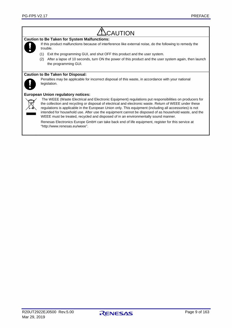
CAUTION Caution to Be Taken for System Malfunctions:
If this product malfunctions because of interference like external noise, do the following to remedy the trouble.
(1) Exit the programming GUI, and shut OFF this product and the user system. (2) After a lapse of 10 seconds, turn ON the power of this product and the user system again, then launch
the programming GUI.
Caution to Be Taken for Disposal:
Penalties may be applicable for incorrect disposal of this waste, in accordance with your national legislation.
European Union regulatory notices: The WEEE (Waste Electrical and Electronic Equipment) regulations put responsibilities on producers for
the collection and recycling or disposal of electrical and electronic waste. Return of WEEE under these regulations is applicable in the European Union only. This equipment (including all accessories) is not intended for household use. After use the equipment cannot be disposed of as household waste, and the WEEE must be treated, recycled and disposed of in an environmentally sound manner. Renesas Electronics Europe GmbH can take back end of life equipment, register for this service at “http://www.renesas.eu/weee”.
PG-FP5 V2.17 PREFACE
R20UT2922EJ0500 Rev.5.00 Page 10 of 163 Mar 29, 2019
Contents PREFACE .......................................................................................................................................................... 3
Important .................................................................................................................................................... 4 Precautions for Safety ................................................................................................................................ 6 Contents ................................................................................................................................................... 10 Terminology .............................................................................................................................................. 13 Term replacement ..................................................................................................................................... 14
1. OVERVIEW.................................................................................................................................................. 15 1.1. Features ............................................................................................................................................ 15 1.2. Writing Quality ................................................................................................................................... 15 1.3. Supported Devices ............................................................................................................................ 15 1.4. Package Components ....................................................................................................................... 16 1.5. FP5 System Overview ....................................................................................................................... 16 1.6. Operating Environment ..................................................................................................................... 18
1.6.1. Hardware environment ............................................................................................................ 18 1.6.2. Software environment ............................................................................................................. 18
1.7. Hardware Specifications .................................................................................................................... 19 1.8. AC Adaptors for PG-FP5 ................................................................................................................... 20 1.9. HCUHEX Files ................................................................................................................................... 20 1.10. Regulatory Compliance Notices ...................................................................................................... 21
2. HARDWARE CONFIGURATION ................................................................................................................. 23 2.1. System Configuration ........................................................................................................................ 23
2.1.1. Host PC ................................................................................................................................... 23 2.1.2. Serial cable.............................................................................................................................. 23 2.1.3. USB cable ............................................................................................................................... 23 2.1.4. AC adaptor .............................................................................................................................. 23 2.1.5. Target cable ............................................................................................................................. 23 2.1.6. GND cable ............................................................................................................................... 24 2.1.7. Target system .......................................................................................................................... 24 2.1.8. Program adaptor ..................................................................................................................... 24
2.2. Names and Functions on Main Unit .................................................................................................. 25 2.2.1. FP5 control panel .................................................................................................................... 25 2.2.2. FP5 connectors ....................................................................................................................... 26
3. SOFTWARE INSTALLATION ...................................................................................................................... 28 3.1. Obtaining Software ............................................................................................................................ 28 3.2. Installation ......................................................................................................................................... 28
3.2.1. Notes on installation ................................................................................................................ 29 3.3. Uninstallation ..................................................................................................................................... 30 3.4. Updating Programming GUI, Firmware and FPGA ........................................................................... 30
3.4.1. Checking the current version .................................................................................................. 30 3.4.2. Installation of programming GUI ............................................................................................. 31 3.4.3. Installation of firmware update ................................................................................................ 31 3.4.4. Installation of FPGA update .................................................................................................... 34
4. USAGE IN STANDALONE MODE .............................................................................................................. 39 4.1. Before Starting Standalone Operation ............................................................................................... 39 4.2. Description of Buttons, Message Display and Status LEDs .............................................................. 39 4.3. Standalone Operation Menu .............................................................................................................. 41
4.3.1. [Commands] menu .................................................................................................................. 41 4.3.2. [Type Setting] menu ................................................................................................................ 43 4.3.3. [Option Setting] menu ............................................................................................................. 44 4.3.4. [Voltage Setting] menu ............................................................................................................ 47 4.3.5. [Utility/Misc.] menu .................................................................................................................. 48
5. USAGE THE REMOTE CONNECTOR ....................................................................................................... 49 5.1. Remote Interface Mode ..................................................................................................................... 49 5.2. Remote Connector Pins .................................................................................................................... 49
PG-FP5 V2.17 PREFACE
R20UT2922EJ0500 Rev.5.00 Page 11 of 163 Mar 29, 2019
5.3. Equivalence Circuits .......................................................................................................................... 50 5.4. External Connection Example ........................................................................................................... 52
6. USAGE COMMUNICATION COMMANDS .................................................................................................. 53 6.1. Starting the Communications Software ............................................................................................. 53 6.2. Command List ................................................................................................................................... 55 6.3. Description of Commands ................................................................................................................. 57 6.4. Description of FP5 Control Commands ............................................................................................. 58
6.4.1. autocon command ................................................................................................................... 58 6.4.2. brt command ........................................................................................................................... 59 6.4.3. conf command ......................................................................................................................... 60 6.4.4. downprm command ................................................................................................................. 63 6.4.5. downset command .................................................................................................................. 63 6.4.6. fcks command ......................................................................................................................... 64 6.4.7. files command ......................................................................................................................... 65 6.4.8. fpga_up command .................................................................................................................. 66 6.4.9. hex command .......................................................................................................................... 67 6.4.10. hlp command ......................................................................................................................... 68 6.4.11. lod command ......................................................................................................................... 69 6.4.12. prm command ....................................................................................................................... 70 6.4.13. progarea command ............................................................................................................... 70 6.4.14. pwr_off command .................................................................................................................. 71 6.4.15. res command ........................................................................................................................ 72 6.4.16. security command ................................................................................................................. 72 6.4.17. selftest command .................................................................................................................. 73 6.4.18. serno command .................................................................................................................... 73 6.4.19. sound command .................................................................................................................... 74 6.4.20. srec command ....................................................................................................................... 75 6.4.21. trc command ......................................................................................................................... 76 6.4.22. upprm command ................................................................................................................... 76 6.4.23. upset command ..................................................................................................................... 77 6.4.24. ver command ........................................................................................................................ 77 6.4.25. version_up command ............................................................................................................ 78
6.5. Description of The FP5 Device Commands ...................................................................................... 80 6.5.1. bln command ........................................................................................................................... 80 6.5.2. clr command ............................................................................................................................ 80 6.5.3. con command .......................................................................................................................... 81 6.5.4. dcon command ........................................................................................................................ 81 6.5.5. ep/epv command ..................................................................................................................... 82 6.5.6. ers command .......................................................................................................................... 83 6.5.7. gdi command ........................................................................................................................... 84 6.5.8. ged command ......................................................................................................................... 86 6.5.9. gid command ........................................................................................................................... 86 6.5.10. glb command ......................................................................................................................... 87 6.5.11. gob command ........................................................................................................................ 88 6.5.12. gof command ........................................................................................................................ 88 6.5.13. gos command ........................................................................................................................ 89 6.5.14. got command ........................................................................................................................ 90 6.5.15. gsc command ........................................................................................................................ 91 6.5.16. gtm command ....................................................................................................................... 91 6.5.17. idc command ......................................................................................................................... 92 6.5.18. opb command ....................................................................................................................... 92 6.5.19. otp command ........................................................................................................................ 93 6.5.20. prg command ........................................................................................................................ 93 6.5.21. read command ...................................................................................................................... 94 6.5.22. rsc command ......................................................................................................................... 95 6.5.23. scf command ......................................................................................................................... 95
PG-FP5 V2.17 PREFACE
R20UT2922EJ0500 Rev.5.00 Page 12 of 163 Mar 29, 2019
6.5.24. sed command ........................................................................................................................ 96 6.5.25. sid command ......................................................................................................................... 96 6.5.26. sig command ......................................................................................................................... 97 6.5.27. slb command ......................................................................................................................... 97 6.5.28. spd command ........................................................................................................................ 98 6.5.29. stm command ........................................................................................................................ 98 6.5.30. sum command ....................................................................................................................... 99 6.5.31. vrf command ......................................................................................................................... 99
7. CONNECTORS AND CABLES.................................................................................................................. 100 7.1. Power Supply Connector ................................................................................................................. 100 7.2. Serial Connector .............................................................................................................................. 101
7.2.1. Serial cable............................................................................................................................ 101 7.3. USB Connector................................................................................................................................ 102
7.3.1. USB cable ............................................................................................................................. 102 7.4. Target Connector ............................................................................................................................. 103
7.4.1. Target cable (16-pin type) ..................................................................................................... 104 7.4.2. Target cable (14-pin type) ..................................................................................................... 106
7.5. GND Connector ............................................................................................................................... 108 7.5.1. GND cable ............................................................................................................................. 108
7.6. Remote Connector .......................................................................................................................... 108 8. NOTES ON TARGET SYSTEM DESIGN .................................................................................................. 109 9. SPECIFICATIONS OF TARGET INTERFACE CIRCUITS ........................................................................ 122
9.1. SO/TxD/IO3/FPDR/FPMD3, RESET and SCK/IO4/FPCK/FPMD4 ................................................ 122 9.2. SI/RxD/FPDT and H/S ..................................................................................................................... 122 9.3. CLK/IO5/FPMD5.............................................................................................................................. 123 9.4. FLMD0/IO0/FPMD0, FLMD1, RFU-1/IO1/FPMD1, and VDE/IO2/FPMD2 ..................................... 123 9.5. VDD and VDD2 .................................................................................................................................... 124 9.6. VPP ................................................................................................................................................... 124
10. TROUBLESHOOTING ............................................................................................................................. 125 10.1. Problems During Startup ............................................................................................................... 125 10.2. Problems During Operation ........................................................................................................... 126
11. MAINTENANCE AND WARRANTY ......................................................................................................... 129 11.1. Maintenance .................................................................................................................................. 129 11.2. Warranty ........................................................................................................................................ 129 11.3. Repair Provisions ........................................................................................................................... 129 11.4. How to Make Request for Repair .................................................................................................. 130
APPENDIX A MESSAGES ............................................................................................................................ 131 A.1. Message Format ............................................................................................................................. 131 A.2. Error/Warning Dialog Boxes for Programming GUI Operation ....................................................... 132 A.3. Information Dialog Boxes for Programming GUI Operation ........................................................... 135 A.4. Error Messages Displayed in FP5 Message Display ...................................................................... 138
APPENDIX B SUPPLEMENTARY INFORMATION....................................................................................... 142 APPENDIX C ELECTRICAL SPECIFICATIONS OF TARGET INTERFACE ................................................ 146
C.1. Absolute Maximum Ratings (TA=0 to 40°C) ................................................................................... 146 C.2. DC Characteristics (TA=0 to 40°C) ................................................................................................. 147 C.3. AC Characteristics (TA=0 to 40°C, C=0pF (Unloaded Condition)) ................................................. 148
C.3.1. CLK output characteristics (TA=0 to 40°C, C=0pF (unloaded condition)) ............................ 149 C.3.2. Serial transfer timing (TA=0 to 40°C, C=0pF (unloaded condition)) ..................................... 150
APPENDIX D ELECTRICAL SPECIFICATIONS OF REMOTE INTERFACE ............................................... 152 D.1. Absolute Maximum Ratings (TA=0 to 40°C) ................................................................................... 152 D.2. DC Characteristics (TA=0 to 40°C, C=0pF (Unloaded Condition)) ................................................. 153 D.3. AC Characteristics (TA=0 to 40°C, C=0pF (Unloaded Condition)) ................................................. 154
D.3.1. Standard mode ..................................................................................................................... 154 D.3.2. Bank mode............................................................................................................................ 156 D.3.3. Simple mode ......................................................................................................................... 158
PG-FP5 V2.17 PREFACE
R20UT2922EJ0500 Rev.5.00 Page 13 of 163 Mar 29, 2019
Terminology The meanings of the terms used in FP5 manual are as follows.
(1) Term Meaning.
FP5 Abbreviation of the flash memory programmer PG-FP5
Programming GUI Windows application to operate FP5 using programming GUI
Target device Renesas Electronics on-chip flash memory microcontroller
Target system User-designed board on which target device is mounted
Program adaptorNote1 Conversion adaptor to write programs to target device
PR5 file Abbreviation of the parameter file for the PG-FP5. The parameter file has parameter information required to write in the flash memory of the target microcontroller. The extension of the file is "*.pr5". Do not change the data in the file. If the file is changed, operation of the FP5 is not guaranteed.
ESF file Abbreviation of the setting file for the PG-FP5. The setting file stores information required for writing. For the FP5, settings regarding the writing environment such as target devices and operation option are stored. The extension of the file is "*.esf". Do not change the data in the file. If the file is changed, operation of the FP5 is not guaranteed.
Note Use ESF files that correspond to the version of the generated FP5. An error occurs when the FP5 reads files from other FP5 versions. In such cases, create new ESF files.
Program file The program file is the program written to the microcontroller. For the FP5, the following file formats are supported. <RL78, 78K, V850> a. Intel HEX format HEX file b. Intel HEX format HCUHEX file c. Motorola S format HEX file d. Motorola S format HCUHEX file <RX family, SuperH family> a. Intel HEX format HEX file b. Motorola S format HEX file c. DDI file <RH850 family, SuperH family> a. Intel HEX format HEX file b. Motorola S format HEX file
Note Addresses may not be consecutive, but they must be in ascending order. Free space will be filled with "FFH" upon download to the FP5. When download is performed with the programming GUI, it has the function to sort addresses in ascending order.
Note For details on the formats, refer to "How to Order ROM Code: Information (C10302E)."
Note The program file name does not support 2-byte characters. Flash options*3 General term for microcontroller operation settings such as security settings
Option data*3 General term for flash options, wide-voltage mode, and full-speed modeNote2
HEX file A HEX file of Intel HEX format type or Motorola HEX format type without option data
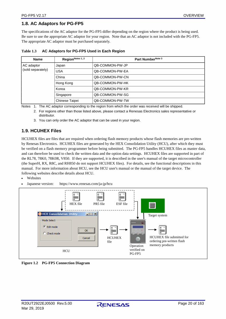
HCUHEX file A HEX file that integrates option data into a HEX file generated by using the HEX Consolidation Utility (HCU), which is used to generate ROM code for flash memory products whose flash memories are pre-written by Renesas Electronics
DDI file File in which data in multiple flash areas generated by Flash Development Toolkit is integrated.
Flash Development Toolkit Flash Development Toolkit is a software to write in the flash memory of the Renesas microcontroller with on-chip flash. For details, refer to the following websites. https://www.renesas.com/fdt
PG-FP5 V2.17 PREFACE
R20UT2922EJ0500 Rev.5.00 Page 14 of 163 Mar 29, 2019
(2) Term Meaning.
INI file File in which settings of the programming GUI are stored. The file is saved when the programming GUI is closed. The file name is "FP5.ini".
OCD security ID*3 Abbreviation of the on-chip debug security ID. Security function for on-chip debugging of the microcontroller.
ID code*3 Authentication code used in the ID authentication mode and in OCD. For details, refer to the user’s manual of the microcontroller.
Lock bit*3 One of the security functions of the microcontroller. For details, refer to the user’s manual of the microcontroller.
Signature Information about the microcontroller (microcontroller name, firmware version)
FINE Supports FINE of the RX100, RX200 and RX65x.
ID authentication mode*3 One of the security functions of the microcontroller. For details, refer to the user’s manual of the microcontroller.
Command protection mode*3
One of the security functions of the microcontroller. For details, refer to the user’s manual of the microcontroller.
OTP*3 One of the security functions of the microcontroller. For details, refer to the user’s manual of the microcontroller.
OFS*3 One of the security functions of the microcontroller. For details, refer to the user’s manual of the microcontroller.
Trusted Memory*3 One of the security functions of the microcontroller. For details, refer to the user’s manual of the microcontroller.
Option-Setting Memory*3 Collective term for registers that determine the state of the MCU after release from reset. For details, refer to the user’s manual of the microcontroller.
Note If a program file includes valid data for any register in the the option-setting memory area, the option-setting memory is set. All bits in sections for which there are no data are filled with“1”.
Notes 1. The program adaptor (FA-xxxx) is a product of Naito Densei Machida Mfg. Co., Ltd. If you have any questions about the FA adaptor board, contact Naito Densei Machida Mfg. Co., Ltd. (Tel:
+81-42-750-4172). 2. The functions that can be used differ depending on the target device. 3. Refer to the user’s manual of the target device for more information. Term replacement When the RX100, RX200 is used, some terms in this manual should be replaced as shown in the table below.
Term Meaning. Get Flash options Access window read
Set Security Access window program
All trademarks and registered trademarks are the property of the respective owner.
PG-FP5 V2.17 OVERVIEW
R20UT2922EJ0500 Rev.5.00 Page 15 of 163 Mar 29, 2019
1. OVERVIEW The FP5 is a tool that erases, writes and verifies programs on a Renesas Electronics on-chip flash memory microcontroller on the target system. 1.1. Features • Compatible with remote operation for FP5 from an external control device • Compatible with communications commands operated by the FP5 command through RS-232C • The customization and security settings of the FP5 unit can be changed with the FP5 Manager function • Supports on-chip 2-power-supply flash memory microcontrollers and single-power-supply on-chip flash memory
microcontrollers • Supports flash memory programming through the programming GUI using the host PC (programming GUI
operation) and operation in standalone (standalone operation) • Supports on-board programming through which programs are written with the target device mounted on the target
system • Program files can be saved in the 16 MB flash memory in the FP5 (divided by 1, in 16 MB units, divided by 2, in 10
MB and 6 MB units, divided by 4, in 4 MB units or divided by 8, in 2 MB units) • Device-specific parameters required for programming can be saved in the FP5 internal flash memory by using the
parameter file (PR5 file), together with programming settings (ESF file). • Multiple program files, PR5 files and ESF files can be saved • Supports CSI, CSI + HS, UART, I2C and PORT as target device interfaces • Can supply VDD and clocks to the target device • Supports USB interface and serial interface (RS-232C) as a host interface • Supports self-testing function • Programming a unique code to a designated area of flash memory 1.2. Writing Quality Thoroughly confirm, verify and evaluate the following points before using the FP5, in order to improve the writing quality. • Design circuits as described in the user’s manual for the target device and the FP5. • Use the device and the FP5 as described in the user’s manual for each product. • The power supplied to the target device is stable. 1.3. Supported Devices The FP5 supports on-chip 2-power-supply flash memory microcontrollers and on-chip single-power-supply flash memory microcontrollers. FP5 parameter files (PR5 files) corresponding to the supported devices are posted on the following website. URLs • Except for Europe area: https://www.renesas.com/pg-fp5 • For Europe area: http://www.renesas.eu/update → Section PG-FP5-EE
PG-FP5 V2.17 OVERVIEW
R20UT2922EJ0500 Rev.5.00 Page 16 of 163 Mar 29, 2019
1.4. Package Components The package of this product includes the items listed below. Check the items. Note that the package for the PG-FP5 does not include an AC adaptor. Purchase an adaptor separately (refer to 1.8 AC Adaptors for PG-FP5). Table 1.1 Package Components
Item Quantity. List of Package 1
PG-FP5 1
USB cable 1
Serial cable 1
Target cable (16pin type) 1
Target cable (14pin type) 1
GND cable 1
PG-FP5 Setup Manual [Japanese / English] 1
Table of Toxic and Hazardous Substance and Elements 1
EMC regulation ( FCC) 1
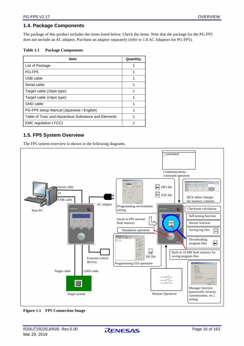
1.5. FP5 System Overview The FP5 system overview is shown in the following diagrams.
Figure 1.1 FP5 Connection Image
Checksum calculation
or
Communications command operation
External control devices
Remote Operation
Manager function (passwords, security, customization, etc.) setting
Saving log files
Target cable
Serial cable
AC adapter
GND cable
Target system
Saved in FP5 internal flash memory
HEX editor changes the memory contents
16MB
Built-in 16 MB flash memory for saving program files
Standalone operation
Downloading program files
INI file
Programming GUI operation
Self-testing function
Buzzer function
USB cable
Host PC
PR5 file
ESF file
Programming environment setting
command
PG-FP5 V2.17 OVERVIEW
R20UT2922EJ0500 Rev.5.00 Page 17 of 163 Mar 29, 2019
<Programming GUI operation> The following operations can be performed with the programming GUI. For USB connection, the USB driver must be installed. The settings on the host PC are saved in an INI file. • ESF file creation • Downloading program files, PR5 files and ESF files (saved into FP5 internal flash memory) • Saving log files • Editing program files (by using HEX editor) • Checksum calculation • Programming command execution • Execution of self-testing function • Manager function (passwords, security, customization, etc.) setting <Standalone operation> The FP5 can operate in standalone mode, whereby commands such as [Erase], [Program] and [Autoprocedure(E.P.)] can be executed without using the host PC. It is suitable for use in production lines during mass production or upgrading programs in the field. The following can be performed in standalone operation. • Execute programming command • Confirm contents of each downloaded file <Communications Command Operation> FP5 can be operated by communications commands from the host PC. <Remote Operation> Writing and PASS/ERROR displays can be operated and confirmed from external control devices. <FP5 internal flash memory> The FP5 has a 16 MB flash memory area for saving program files. This memory area can be used as two programming areas of 10 MB and 6 MB (Area 0 to Area 1), four 4 MB programming areas (Area 0 to Area 3), or eight independent 2 MB programming areas (Area 0 to Area 7). Program files can be downloaded to each programming area, and which file, PR5 or ESF, is to be saved is selectable in programming area units. That is, files can be individually downloaded in each programming area, and the area used can also be selected individually. Program files, PR5 files and ESF files are retained even if the FP5 power is turned off. Downloaded data will be self-tested for accuracy when the FP5 is started, during downloads and when programming areas are changed. <Notification function> When Autoprocedure (E.P.) is executed, whether execution is completed normally is indicated by beeps. <Checksum calculation> Checksum calculation for the download program files is possible.
PG-FP5 V2.17 OVERVIEW
R20UT2922EJ0500 Rev.5.00 Page 18 of 163 Mar 29, 2019
1.6. Operating Environment 1.6.1. Hardware environment
(1) Host PCs • PC/AT compatible • Equipped with USB 2.0 ports (compatible with 1.1) • Equipped with RS-232C serial ports 1.6.2. Software environment
(1) OS (either of the following) • Windows 7 (32-bit edition, 64-bit edition) • Windows 8.1 (32-bit edition, 64-bit edition) • Windows 10 (32-bit edition, 64-bit edition) • Microsoft .NET Framework 4 • Microsoft Visual C++ 2010 Redistributable Package (x86) • Internet Explorer 6.0 or later
PG-FP5 V2.17 OVERVIEW
R20UT2922EJ0500 Rev.5.00 Page 19 of 163 Mar 29, 2019
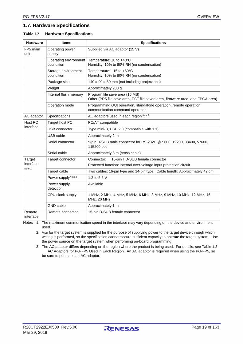
1.7. Hardware Specifications Table 1.2 Hardware Specifications
Hardware Items Specifications FP5 main unit
Operating power supply
Supplied via AC adaptor (15 V)
Operating environment ccondition
Temperature: ±0 to +40°C Humidity: 10% to 80% RH (no condensation)
Storage environment ccondition
Temperature: −15 to +60°C Humidity: 10% to 80% RH (no condensation)
Package size 140 × 90 × 30 mm (not including projections)
Weight Approximately 230 g
Internal flash memory Program file save area (16 MB) Other (PR5 file save area, ESF file saved area, firmware area, and FPGA area)
Operation mode Programming GUI operation, standalone operation, remote operation, communication command operation
AC adaptor Specifications AC adaptors used in each regionNote 3
Host PC interface
Target host PC PC/AT compatible
USB connector Type mini-B, USB 2.0 (compatible with 1.1)
USB cable Approximately 2 m
Serial connector 9-pin D-SUB male connector for RS-232C @ 9600, 19200, 38400, 57600, 115200 bps
Serial cable Approximately 3 m (cross cable)
Target interface Note 1
Target connector Connector: 15-pin HD-SUB female connector Protected function: Internal over-voltage input protection circuit
Target cable Two cables: 16-pin type and 14-pin type. Cable length: Approximately 42 cm
Power supplyNote 2 1.2 to 5.5 V
Power supply detection
Available
CPU clock supply 1 MHz, 2 MHz, 4 MHz, 5 MHz, 6 MHz, 8 MHz, 9 MHz, 10 MHz, 12 MHz, 16 MHz, 20 MHz
GND cable Approximately 1 m
Remote interface
Remote connector 15-pin D-SUB female connector
Notes 1. The maximum communication speed in the interface may vary depending on the device and environment used.
2. VDD for the target system is supplied for the purpose of supplying power to the target device through which writing is performed, so the specification cannot secure sufficient capacity to operate the target system. Use the power source on the target system when performing on-board programming.
3. The AC adaptor differs depending on the region where the product is being used. For details, see Table 1.3 AC Adaptors for PG-FP5 Used in Each Region. An AC adaptor is required when using the PG-FP5, so be sure to purchase an AC adaptor.
PG-FP5 V2.17 OVERVIEW
R20UT2922EJ0500 Rev.5.00 Page 20 of 163 Mar 29, 2019
1.8. AC Adaptors for PG-FP5 The specifications of the AC adaptor for the PG-FP5 differ depending on the region where the product is being used. Be sure to use the appropriate AC adaptor for your region. Note that an AC adaptor is not included with the PG-FP5. The appropriate AC adaptor must be purchased separately. Table 1.3 AC Adaptors for PG-FP5 Used in Each Region
Name RegionNotes 1, 2 Part NumberNote 3 AC adaptor (sold separately)
Japan QB-COMMON-PW-JP
USA QB-COMMON-PW-EA
China QB-COMMON-PW-CN
Hong Kong QB-COMMON-PW-HK
Korea QB-COMMON-PW-KR
Singapore QB-COMMON-PW-SG
Chinese Taipei QB-COMMON-PW-TW Notes 1. The AC adaptor corresponding to the region from which the order was received will be shipped. 2. For regions other than those listed above, please contact a Renesas Electronics sales representative or
distributor. 3. You can only order the AC adaptor that can be used in your region. 1.9. HCUHEX Files HCUHEX files are files that are required when ordering flash memory products whose flash memories are pre-written by Renesas Electronics. HCUHEX files are generated by the HEX Consolidation Utility (HCU), after which they must be verified on a flash memory programmer before being submitted. The PG-FP5 handles HCUHEX files as master data, and can therefore be used to check the written data and the option data settings. HCUHEX files are supported in part of the RL78, 78K0, 78K0R, V850. If they are supported, it is described in the user's manual of the target microcontroller (the SuperH, RX, R8C, and RH850 do not support HCUHEX files). For details, see the functional descriptions in this manual. For more information about HCU, see the HCU user's manual or the manual of the target device. The following websites describe details about HCU. • Websites • Japanese version: https://www.renesas.com/ja-jp/hcu
Figure 1.2 PG-FP5 Connection Diagram
PR5 file ESF file HEX file
HCU
HCUHEX file
Operation verified on PG-FP5
Target system
HCUHEX file submitted for ordering pre-written flash memory products
PG-FP5 V2.17 OVERVIEW
R20UT2922EJ0500 Rev.5.00 Page 21 of 163 Mar 29, 2019
1.10. Regulatory Compliance Notices
This equipment complies with the EMC protection requirements
WARNING This is a ‘Class A’ (EN 55022: 1998) equipment. This equipment can cause radio frequency noise when used in the residential area. In such cases, the user/operator of the equipment may be required to take appropriate countermeasures under his responsibility.
EEDT-ST-001-11
CAUTION
This equipment should be handled like a CMOS semiconductor device. The user must take all precautions to avoid build-up of static electricity while working with this equipment. All test and measurement tool including the workbench must be grounded. The user/operator must be grounded using the wrist strap. The connectors and/or device pins should not be touched with bare hands.
EEDT-ST-004-10
For customers in the European Union only
Redemption of Waste Electrical and Electronic Equipment (WEEE) in accordance with legal regulations applicable in the European Union only: This equipment (including all accessories) is not intended for household use. After use the equipment cannot be disposed of as household waste. Renesas Electronics Europe GmbH offers to take back the equipment. All you need to do is register at http://www.renesas.eu/weee.
PG-FP5 V2.17 OVERVIEW
R20UT2922EJ0500 Rev.5.00 Page 22 of 163 Mar 29, 2019
EMC regulation (FCC) FCC Certifications: Note: This equipment has been tested and found to comply with the limits for a Class A digital device, pursuant to part 15 of the FCC Rules. These limits are designed to provide reasonable protection against harmful interference when the equipment is operated in a commercial environment. This equipment generates, uses and can radiate radio frequency energy and, if not installed and used in accordance with the instruction manual, may cause harmful interference to radio communications. Operation of this equipment in a residential area is likely to cause harmful interference in which case the user will be required to correct the interference at his own expense. Modifications not expressly approved by the manufacturer could void the user's authority to operated the equipment under FCC rules.
CAUTION: When you use the product which need AC adapter, please use AC adapter which comply with the standard of FCC, indicated by User’s Manual.
PG-FP5 V2.17 HARDWARE CONFIGURATION
R20UT2922EJ0500 Rev.5.00 Page 23 of 163 Mar 29, 2019
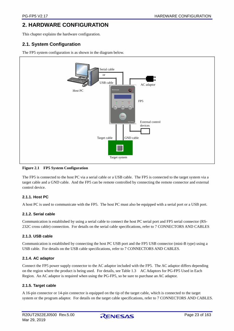
2. HARDWARE CONFIGURATION This chapter explains the hardware configuration. 2.1. System Configuration The FP5 system configuration is as shown in the diagram below.
Figure 2.1 FP5 System Configuration
The FP5 is connected to the host PC via a serial cable or a USB cable. The FP5 is connected to the target system via a target cable and a GND cable. And the FP5 can be remote controlled by connecting the remote connector and external control device. 2.1.1. Host PC
A host PC is used to communicate with the FP5. The host PC must also be equipped with a serial port or a USB port. 2.1.2. Serial cable
Communication is established by using a serial cable to connect the host PC serial port and FP5 serial connector (RS-232C cross cable) connection. For details on the serial cable specifications, refer to 7 CONNECTORS AND CABLES 2.1.3. USB cable
Communication is established by connecting the host PC USB port and the FP5 USB connector (mini-B type) using a USB cable. For details on the USB cable specifications, refer to 7 CONNECTORS AND CABLES. 2.1.4. AC adaptor
Connect the FP5 power supply connector to the AC adaptor included with the FP5. The AC adaptor differs depending on the region where the product is being used. For details, see Table 1.3 AC Adaptors for PG-FP5 Used in Each Region. An AC adaptor is required when using the PG-FP5, so be sure to purchase an AC adaptor. 2.1.5. Target cable
A 16-pin connector or 14-pin connector is equipped on the tip of the target cable, which is connected to the target system or the program adaptor. For details on the target cable specifications, refer to 7 CONNECTORS AND CABLES.
External control devices
Target cable
Serial cable
AC adaptor
GND cable
Target system
USB cable
Host PC
FP5
or
PG-FP5 V2.17 HARDWARE CONFIGURATION
R20UT2922EJ0500 Rev.5.00 Page 24 of 163 Mar 29, 2019
2.1.6. GND cable
To reinforce the GND, use a GND cable to connect the FP5 GND connector and the signal GND of the target system or program adaptor. For details on the GND cable specifications, refer to 7 CONNECTORS AND CABLES. Note The FP5 and target system may be damaged if the voltage between the FP5 GND and the target system GND is
different. Use the GND cable to match the voltage before connecting the target cable. 2.1.7. Target system
The target system must be equipped with a device interface that complies with the target cable specifications. For details on the specifications, refer to 7 CONNECTORS AND CABLES, 8 NOTES ON TARGET SYSTEM DESIGN, and 9 SPECIFICATIONS OF TARGET INTERFACE CIRCUITS. 2.1.8. Program adaptor
The FP5 supports off-board programming through which programs are written via a program adaptor without mounting the target device onto the target system.
PG-FP5 V2.17 HARDWARE CONFIGURATION
R20UT2922EJ0500 Rev.5.00 Page 25 of 163 Mar 29, 2019
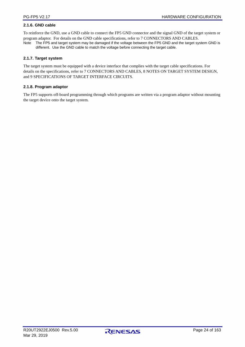
2.2. Names and Functions on Main Unit This section describes the names and functions on the FP5 main unit. 2.2.1. FP5 control panel
Indicators and buttons are laid out on the FP5 top.
Figure 2.2 FP5 Top View <Control Panel>
(1) Indicators • POWER LED LED that displays the FP5 power status.
A red LED is turned on when the FP5 is ON, and is turned off when the FP5 is OFF. • Message display An LCD display of 16 × 2-characters that indicates the operating mode or menus.
It is mainly used when the FP5 operates in standalone mode. • Status LEDs LEDs that show the FP5 operating status.
PASS (green LED turned on) indicates normal completion, BUSY (orange LED flashes) indicates processing in progress, and ERROR (red LED turned on) indicates abnormal completion.
(2) Buttons • POWER button Used to turn on/off the power to the FP5. Press this button longer (for about 1 minute)
when turning on/off. • NEXT button Proceeds to the next menu item at the same level in sequence. • ENTER button Selects the item shown in the message display. • CANCEL button Cancels the current selection and returns to the previous menu item. The command
currently running cannot be stopped, except for the [Read] command. • START button Executes the [Autoprocedure(E.P.)] command with a valid programming area setting. Note The NEXT, ENTER, CANCEL and START buttons are mainly used in standalone mode. When the FP5 Manager is used to switch to the bank mode or simple mode, the button functions and message
display functions will change. Refer to each microcontroller edition 1.3.2 [FP5 Manager] command and 5 USAGE THE REMOTE CONNECTOR.
Control buttons
Status LEDs
Message display POWER button
POWER LED
PG-FP5 V2.17 HARDWARE CONFIGURATION
R20UT2922EJ0500 Rev.5.00 Page 26 of 163 Mar 29, 2019
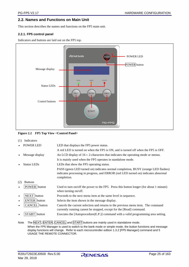
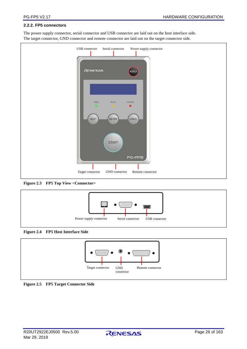
2.2.2. FP5 connectors
The power supply connector, serial connector and USB connector are laid out on the host interface side. The target connector, GND connector and remote connector are laid out on the target connector side.
Figure 2.3 FP5 Top View <Connector>
Figure 2.4 FP5 Host Interface Side
Figure 2.5 FP5 Target Connector Side
Target connector GND connector
Remote connector
Power supply connector USB connector Serial connector
USB connector Serial connector Power supply connector
Target connector GND connector Remote connector
PG-FP5 V2.17 HARDWARE CONFIGURATION
R20UT2922EJ0500 Rev.5.00 Page 27 of 163 Mar 29, 2019
(1) Power supply connector Connect the power supply connector to the AC adaptor. For details on the power supply connector specifications, refer to 7 CONNECTORS AND CABLES.
Note Do not use an AC adaptor other than that included with the PG-FP5. (2) Serial connector
Communication is established by using a serial cable (RS-232C cross cable) connection to connect the host PC serial port and FP5 serial connector. The data transfer conditions are as follows. • Data transfer speed: 9,600 bps, 19,200 bps, 38,400 bps, 57,600 bps, or 115,200 bps • Data bit: 8 bits • Parity: none • Stop bit: 1 bit • Flow control: hardware The transfer speed is set to 9,600 bps by default, but it can be changed. For details on the serial connector specifications, refer to 7 CONNECTORS AND CABLES.
(3) USB connector
Communication is established by using a USB cable to connect the host PC USB port and the FP5 USB connector (mini-B type). This connector conforms with USB 2.0 standards. For details on the USB connector specifications, refer to 7 CONNECTORS AND CABLES.
(4) Target connector
Connect the target connector to the target system using the target cable for on-board programming. Connect the target connector to the program adaptor using the target cable for off-board programming. For details on the target connector specifications, refer to 7 CONNECTORS AND CABLES.
(5) GND connector
To reinforce the GND, connect the FP5 GND connector and the signal GND of the target system or program adaptor using a GND cable. For details on the GND connector specifications, refer to 7 CONNECTORS AND CABLES.
Note The FP5 and target system may be damaged if the voltage between the FP5 GND and the target system GND is different. Use the GND cable to match the voltage before connecting the target cable.
(6) Remote connector
The FP5 can be remote controlled by connecting the remote connector and external control device. For details on the Remote operation, refer to 5 USAGE THE REMOTE CONNECTOR, 7 CONNECTORS AND CABLES.
PG-FP5 V2.17 SOFTWARE INSTALLATION
R20UT2922EJ0500 Rev.5.00 Page 28 of 163 Mar 29, 2019
3. SOFTWARE INSTALLATION This chapter explains the software installation. 3.1. Obtaining Software Download the programming GUI, USB driver, and FP5 parameter file (PR5 file) from the following Renesas Electronics website. URLs • Except for Europe area: https://www.renesas.com/pg-fp5 • For Europe area: http://www.renesas.eu/update → Section PG-FP5-EE Note Use of the latest version of software is recommended to assure the FP5 operation. 3.2. Installation This section explains the installation procedure for the programming GUI, USB driver and parameter file (PR5 file). Table 3.1 Installation
Installation Order Item Method 1 Programming
GUI, USB driver Run the downloaded executable file (PG-FP5_Package_Vxxx.exe) and perform installation, following the directions on the installer screen. After installation, the USB driver detects the FP5 by plug-and-play, and it is automatically added.
2 PR5 file Decompress the downloaded file to any folder. A *.pr5 file is decompressed into any folder, so copy it to the FP5_PRJ folder where the programming GUI is installed.
The folder configuration after programming GUI installation is as follows.
\Program Files C:\
\Renesas Electronics \Programming Tools
\PG-FP5 V2.07 [FP5.exe]
\Doc \PG-FP5 V2.08
Folder specified as the installation destination (C:\Program Files\Common Files (x86)\Renesas Electronics for the 64-bit version of Windows)
Folder where programming GUI is stored
Folder where documents are stored
USB driver storage folder (\USB_Driver_x64 for the 64-bit version of Windows) \MCU Tools Drivers
\PG-FP5
PG-FP5 V2.17 SOFTWARE INSTALLATION
R20UT2922EJ0500 Rev.5.00 Page 29 of 163 Mar 29, 2019
3.2.1. Notes on installation
(1) Multiple versions of the PG-FP5 can be installed on a single host PC. Although we recommend using the latest version of any development tool, leaving a previous version on your host PC and then installing the latest version lets you easily switch the development environment.
(2) You might be asked to reboot your computer after installing the PG-FP5. Be sure to close all other applications before rebooting your computer.
(3) You must have administrator privileges to install the PG-FP5. (4) The PG-FP5 can only be installed in a folder that is named using ASCII characters. (Note that the 11 characters /
* : < > ? | " \ ; , and character strings that begin and end with a space cannot be used.) The PG-FP5 might not operate correctly if installed in a folder that is named using other characters.
(5) The PG-FP5 cannot be installed from a network drive or on a network drive. (6) The installer does not specify environment variable paths. If these paths are required, add them after installation. (7) The Microsoft .NET Framework and the Microsoft Visual C++ runtime libraries are required to run the installer. If
the Microsoft .NET Framework or the Microsoft Visual C++ runtime libraries are not installed, the programming GUI will install them.
(8) Make sure that your host PC is connected to the network before installing the program. If you wish to install the program on a host PC that is not connected to the network, first go to the Microsoft Download Center and install the Microsoft .NET Framework 4 before installing programming GUI.
(9) If the installer is started on a non-Japanese version of Windows, then if the path contains multi-byte characters it will cause an error, and the installer will not start.
(10) The following folders created after installation (including the files under the folders) contain files required for the tools to operate. Do not delete them.
(Windows is the 32-bit edition and the system drive is C:) C:\Program Files\Common Files\Renesas Electronics CubeSuite+\ (Windows is the 64-bit edition and the system drive is C:) C:\Program Files\Common Files (x86)\Renesas Electronics CubeSuite+\
(11) To change the folder of the installed tools, uninstall all the CS+ related software and the programming GUI for PG-FP5, and install them again.
(12) In the environment where the programming GUI for CS+ and PG-FP5 and USB driver for PG-FP5 are installed, the programming GUI for PG-FP5 and USB driver for PG-FP5 are included in the target software of the CS+ integrated uninstaller. If you don’t want to delete them, remove them from the uninstallation targets.
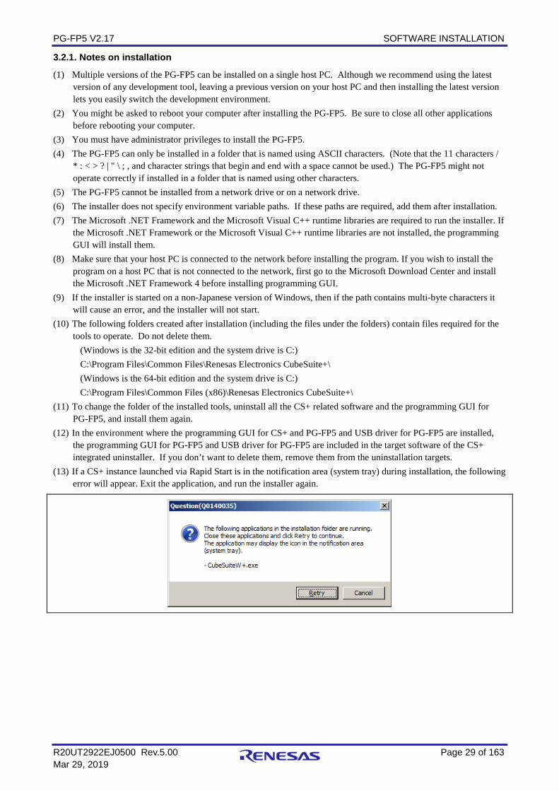
(13) If a CS+ instance launched via Rapid Start is in the notification area (system tray) during installation, the following error will appear. Exit the application, and run the installer again.
PG-FP5 V2.17 SOFTWARE INSTALLATION
R20UT2922EJ0500 Rev.5.00 Page 30 of 163 Mar 29, 2019
3.3. Uninstallation This section explains how to uninstall the programming GUI, USB driver, parameter file (PR5 file), customized setup file (ESF file) and setting information file (INI file). The uninstallation order is prescribed. Table 3.2 Uninstallation
Item Method Programming GUI, USB driver
Open [Add or Remove Programs] on the Control Panel and uninstall this program. The names are [PG-FP5 Vx.xx] and [USB Driver x86T for Renesas MCU Tools] (or [USB Driver x64 for Renesas MCU Tools]). Parameter files (*.pr5), setting files (*.esf), and INI file (FP5.ini) are not deleted.
PR5 file Delete PR5 files (*.pr5) stored in the FP5_PRJ folder in the programming GUI installation folder.
ESF file Delete ESF files (*.esf) stored in the FP5_PRJ folder in the programming GUI installation folder, or other folder.
3.4. Updating Programming GUI, Firmware and FPGA The firmware and FPGA are programs embedded in the device for controlling the FP5. Updating the programming GUI, firmware and FPGA enables the following. • Addition of newly supported functions or devices • Correction of restrictions Use of the latest versions of the programming GUI, firmware and FPGA are recommended to assure the FP5 operation. The latest versions are available on the following websites. URLs • Except for Europe area: https://www.renesas.com/pg-fp5 • For Europe area: http://www.renesas.eu/update → Section PG-FP5-EE Note If update of firmware and FPGA is improperly performed, FP5 may no longer operate. Refer to the following
procedure or method for updating. Note If the firmware or FPGA is updated, the PR5 file, ESF file or program file may be deleted. In such cases,
download the PR5 file, ESF file or program file again. Be sure to follow the procedure below when updating the firmware and FPGA. 1. Check the current version. (Refer to 3.4.1 Checking the current version.) 2. If not the latest version, update the programming GUI. (Refer to 3.4.2 Installation of programming GUI.) 3. Update the firmware using the latest programming GUI. (Refer to 3.4.3 Installation of firmware update.) 4. Update the FPGA using the programming GUI. (Refer to 3.4.4 Installation of FPGA update.) 3.4.1. Checking the current version
(1) Open the main window of the programming GUI. (Refer to each microcontroller edition 1.1 Introduction.) (2) Check the versions of the programming GUI, firmware and FPGA, as shown below.
Programming GUI: [Help] menu → [About] Firmware: [Programmer] menu → [Reset] commandNote FPGA: [Programmer] menu → [Reset] commandNote
Note Display example of [Reset] command Firmware Version Vx.xx Board H/W Vx, FPGA Vx Serial No.: XXXXXXXXXX Standard mode usecured
←Firmware version ←FPGA version
(3) The latest versions are available on the following websites. URLs • Except for Europe area: https://www.renesas.com/pg-fp5 • For Europe area: http://www.renesas.eu/update → Section PG-FP5-EE
PG-FP5 V2.17 SOFTWARE INSTALLATION
R20UT2922EJ0500 Rev.5.00 Page 31 of 163 Mar 29, 2019
3.4.2. Installation of programming GUI
Run the downloaded executable file (PG-FP5_Package_Vxxx.exe). Perform installation, following the directions on the installer screen. 3.4.3. Installation of firmware update
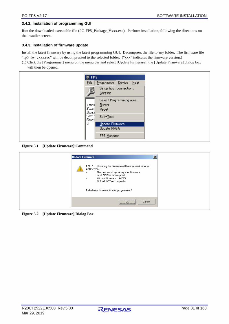
Install the latest firmware by using the latest programming GUI. Decompress the file to any folder. The firmware file “fp5_fw_vxxx.rec” will be decompressed to the selected folder. (“xxx” indicates the firmware version.) (1) Click the [Programmer] menu on the menu bar and select [Update Firmware]; the [Update Firmware] dialog box
will then be opened.
Figure 3.1 [Update Firmware] Command
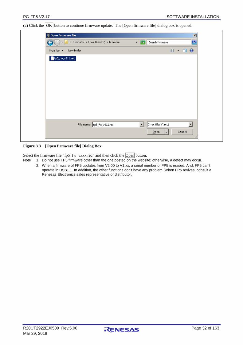
Figure 3.2 [Update Firmware] Dialog Box
PG-FP5 V2.17 SOFTWARE INSTALLATION
R20UT2922EJ0500 Rev.5.00 Page 32 of 163 Mar 29, 2019
(2) Click the OK button to continue firmware update. The [Open firmware file] dialog box is opened.
Figure 3.3 [Open firmware file] Dialog Box
Select the firmware file “fp5_fw_vxxx.rec” and then click the Open button. Note 1. Do not use FP5 firmware other than the one posted on the website; otherwise, a defect may occur. 2. When a firmware of FP5 updates from V2.00 to V1.xx, a serial number of FP5 is erased. And, FP5 can't
operate in USB1.1. In addition, the other functions don't have any problem. When FP5 revives, consult a Renesas Electronics sales representative or distributor.
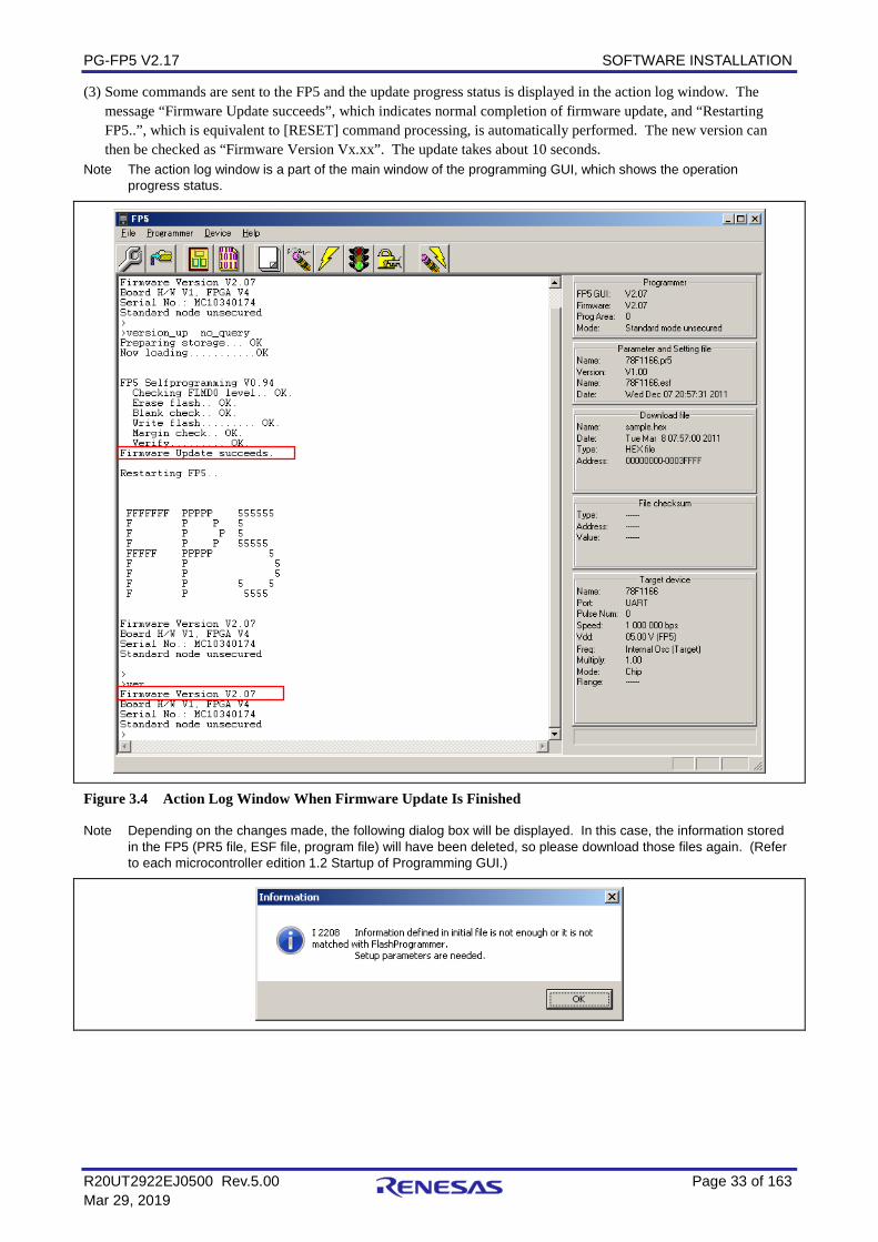
PG-FP5 V2.17 SOFTWARE INSTALLATION
R20UT2922EJ0500 Rev.5.00 Page 33 of 163 Mar 29, 2019
(3) Some commands are sent to the FP5 and the update progress status is displayed in the action log window. The message “Firmware Update succeeds”, which indicates normal completion of firmware update, and “Restarting FP5..”, which is equivalent to [RESET] command processing, is automatically performed. The new version can then be checked as “Firmware Version Vx.xx”. The update takes about 10 seconds.
Note The action log window is a part of the main window of the programming GUI, which shows the operation progress status.
Figure 3.4 Action Log Window When Firmware Update Is Finished
Note Depending on the changes made, the following dialog box will be displayed. In this case, the information stored in the FP5 (PR5 file, ESF file, program file) will have been deleted, so please download those files again. (Refer to each microcontroller edition 1.2 Startup of Programming GUI.)
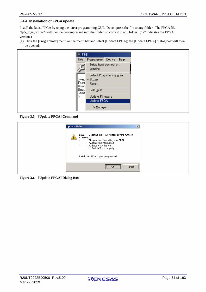
PG-FP5 V2.17 SOFTWARE INSTALLATION
R20UT2922EJ0500 Rev.5.00 Page 34 of 163 Mar 29, 2019
3.4.4. Installation of FPGA update
Install the latest FPGA by using the latest programming GUI. Decompress the file to any folder. The FPGA file “fp5_fpga_vx.rec” will then be decompressed into the folder, so copy it to any folder. (“x” indicates the FPGA version.) (1) Click the [Programmer] menu on the menu bar and select [Update FPGA]; the [Update FPGA] dialog box will then
be opened.
Figure 3.5 [Update FPGA] Command
Figure 3.6 [Update FPGA] Dialog Box
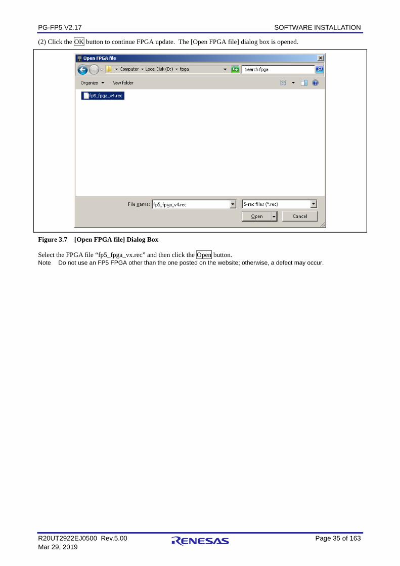
PG-FP5 V2.17 SOFTWARE INSTALLATION
R20UT2922EJ0500 Rev.5.00 Page 35 of 163 Mar 29, 2019
(2) Click the OK button to continue FPGA update. The [Open FPGA file] dialog box is opened.
Figure 3.7 [Open FPGA file] Dialog Box
Select the FPGA file “fp5_fpga_vx.rec” and then click the Open button. Note Do not use an FP5 FPGA other than the one posted on the website; otherwise, a defect may occur.
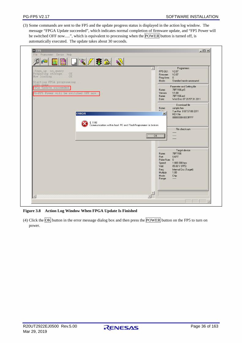
PG-FP5 V2.17 SOFTWARE INSTALLATION
R20UT2922EJ0500 Rev.5.00 Page 36 of 163 Mar 29, 2019
(3) Some commands are sent to the FP5 and the update progress status is displayed in the action log window. The message “FPGA Update succeeded”, which indicates normal completion of firmware update, and “FP5 Power will be switched OFF now.....”, which is equivalent to processing when the POWER button is turned off, is automatically executed. The update takes about 30 seconds.
Figure 3.8 Action Log Window When FPGA Update Is Finished
(4) Click the OK button in the error message dialog box and then press the POWER button on the FP5 to turn on power.
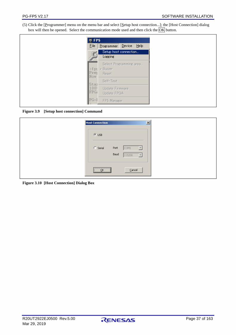
PG-FP5 V2.17 SOFTWARE INSTALLATION
R20UT2922EJ0500 Rev.5.00 Page 37 of 163 Mar 29, 2019
(5) Click the [Programmer] menu on the menu bar and select [Setup host connection...]; the [Host Connection] dialog box will then be opened. Select the communication mode used and then click the OK button.
Figure 3.9 [Setup host connection] Command
Figure 3.10 [Host Connection] Dialog Box
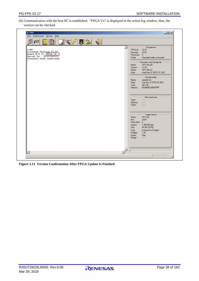
PG-FP5 V2.17 SOFTWARE INSTALLATION
R20UT2922EJ0500 Rev.5.00 Page 38 of 163 Mar 29, 2019
(6) Communication with the host PC is established. “FPGA Vx” is displayed in the action log window; thus, the version can be checked.
Figure 3.11 Version Confirmation After FPGA Update Is Finished
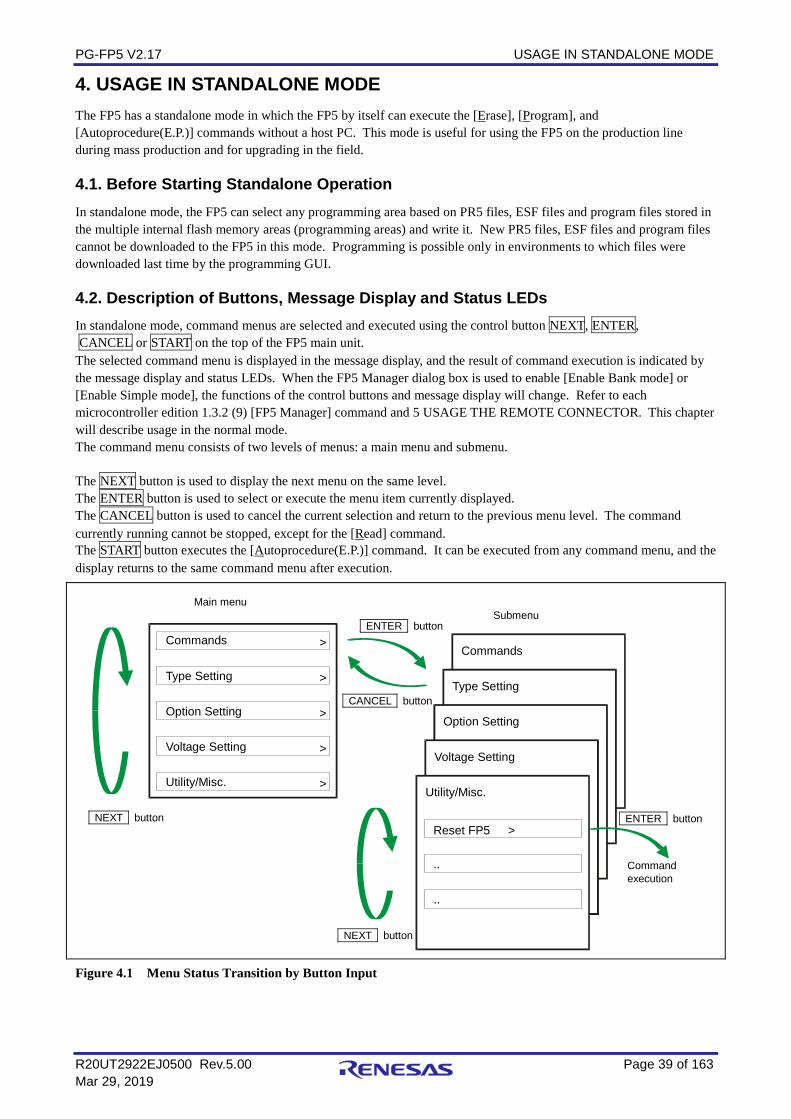
PG-FP5 V2.17 USAGE IN STANDALONE MODE
R20UT2922EJ0500 Rev.5.00 Page 39 of 163 Mar 29, 2019
4. USAGE IN STANDALONE MODE The FP5 has a standalone mode in which the FP5 by itself can execute the [Erase], [Program], and [Autoprocedure(E.P.)] commands without a host PC. This mode is useful for using the FP5 on the production line during mass production and for upgrading in the field. 4.1. Before Starting Standalone Operation In standalone mode, the FP5 can select any programming area based on PR5 files, ESF files and program files stored in the multiple internal flash memory areas (programming areas) and write it. New PR5 files, ESF files and program files cannot be downloaded to the FP5 in this mode. Programming is possible only in environments to which files were downloaded last time by the programming GUI. 4.2. Description of Buttons, Message Display and Status LEDs In standalone mode, command menus are selected and executed using the control button NEXT, ENTER, CANCEL or START on the top of the FP5 main unit. The selected command menu is displayed in the message display, and the result of command execution is indicated by the message display and status LEDs. When the FP5 Manager dialog box is used to enable [Enable Bank mode] or [Enable Simple mode], the functions of the control buttons and message display will change. Refer to each microcontroller edition 1.3.2 (9) [FP5 Manager] command and 5 USAGE THE REMOTE CONNECTOR. This chapter will describe usage in the normal mode. The command menu consists of two levels of menus: a main menu and submenu. The NEXT button is used to display the next menu on the same level. The ENTER button is used to select or execute the menu item currently displayed. The CANCEL button is used to cancel the current selection and return to the previous menu level. The command currently running cannot be stopped, except for the [Read] command. The START button executes the [Autoprocedure(E.P.)] command. It can be executed from any command menu, and the display returns to the same command menu after execution.
Commands
Main menu
Submenu
Commands
Voltage Setting
Utility/Misc.
Option Setting
Type Setting
>
>
>
>
>
Reset FP5 >
..
..
Type Setting
Option Setting
Voltage Setting
Utility/Misc.
ENTER button
CANCEL button
NEXT button
NEXT button
ENTER button
Command execution
Figure 4.1 Menu Status Transition by Button Input
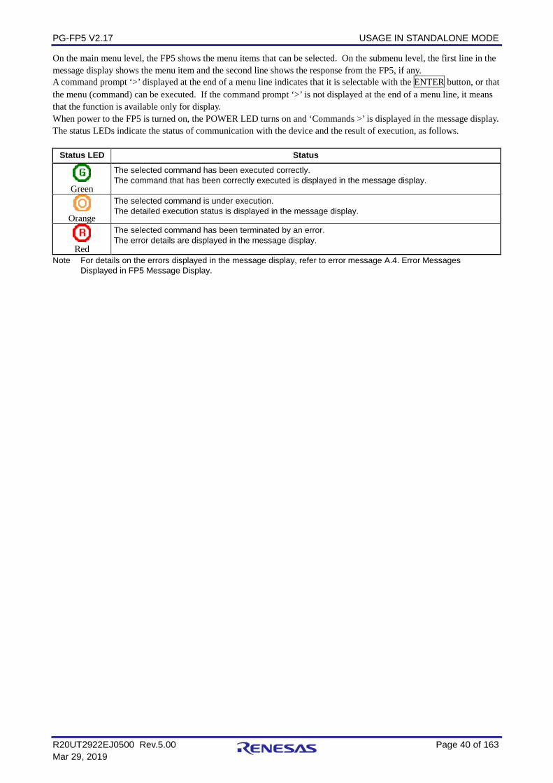
PG-FP5 V2.17 USAGE IN STANDALONE MODE
R20UT2922EJ0500 Rev.5.00 Page 40 of 163 Mar 29, 2019
On the main menu level, the FP5 shows the menu items that can be selected. On the submenu level, the first line in the message display shows the menu item and the second line shows the response from the FP5, if any. A command prompt ‘>’ displayed at the end of a menu line indicates that it is selectable with the ENTER button, or that the menu (command) can be executed. If the command prompt ‘>’ is not displayed at the end of a menu line, it means that the function is available only for display. When power to the FP5 is turned on, the POWER LED turns on and ‘Commands >’ is displayed in the message display. The status LEDs indicate the status of communication with the device and the result of execution, as follows.
Status LED Status
Green
The selected command has been executed correctly. The command that has been correctly executed is displayed in the message display.
Orange
The selected command is under execution. The detailed execution status is displayed in the message display.
Red
The selected command has been terminated by an error. The error details are displayed in the message display.
Note For details on the errors displayed in the message display, refer to error message A.4. Error Messages Displayed in FP5 Message Display.
PG-FP5 V2.17 USAGE IN STANDALONE MODE
R20UT2922EJ0500 Rev.5.00 Page 41 of 163 Mar 29, 2019
4.3. Standalone Operation Menu In standalone mode, the programming environment of the target device can be checked and then programs can be written by using the commands explained in this section. 4.3.1. [Commands] menu
The [Commands] menu provides various commands required for programming the target device. Select a command from this menu and press the ENTER button; the FP5 will then execute the command for the target device, based on the settings downloaded to the valid programming area. For details on command execution, refer to each microcontroller edition 1.3.3[Device] menu. Table 4.1 [Commands] Menu (1)
Main Menu Submenu Description [Commands >] [E.P. >] Pressing the ENTER button executes the [Autoprocedure(E.P.)]
command.
[Program >] Pressing the ENTER button executes the [Program] command.
[Erase >] Pressing the ENTER button executes the [Erase] command.
[Verify >] Pressing the ENTER button executes the [Verify] command.
[Set Security >] Pressing the ENTER button executes the [Set Security] command.
[Checksum >] Pressing the ENTER button executes the [Checksum] command. The checksum value read from the target device is displayed in the message display. <When a product with no data flash is selected from the 78K/V850/RL78 family> Checksum:xxxx <When a product with data flash is selected from the 78K/V850/RL78 family> Code Flash sum: xxxx -> Enter Click the ENTER button. Data Flash sum: xxxx -> Enter Click the ENTER button. Total sum: xxxx -> Enter <When RX family, RH850 family, R8C family, or SuperH family is selected> User mat sum: xxxxxxxx -> Enter Click the ENTER button. Data mat sum: xxxxxxxx -> Enter Click the ENTER button. UB mat sum: xxxxxxxx -> Enter Click the ENTER button. Total sum: xxxxxxxx -> Enter The comparison result is also displayed if [Enable checksum compare function] in FP5 management setting is enabled. Checksum: Compare:PASS (or ERROR)
PG-FP5 V2.17 USAGE IN STANDALONE MODE
R20UT2922EJ0500 Rev.5.00 Page 42 of 163 Mar 29, 2019
Table 4.1 [Commands] Menu (2)
Main Menu Submenu Description [Commands >] [Set Lock bits >] Pressing the ENTER button executes the [Set Lock bits] command.
[Set OptionBytes >] Pressing the ENTER button executes the [Set Option bytes] command.
[Set OCD-Sec-ID >] Pressing the ENTER button executes the [Set ID Code] command.
[Set ID Code >] Pressing the ENTER button executes the [Set ID Code] command.
[Set Lock bits >] Pressing the ENTER button executes the [Set Lock bits] command.
[Blank check >] Pressing the ENTER button executes the [Blank check] command.
[Signature >] Pressing the ENTER button executes the [Signature read] command. The device name is displayed in the message display. Display example: Signature: D78F1166
[Connect >] Pressing the ENTER button executes the con command. Issuing the autocon command “autocon off” causes display of this item in the submenu while the autocon command “autocon on” removes it from the submenu. For more information on the function, refer to chapter 6, Using Communications Commands.
[Disconnect >] Pressing the ENTER button executes the dcon command. autoconコマンドで“autocon off”を実行するとサブメニューに表示されるようになり,“autocon on”を実行するとサブメニューに表示されなくなります。機能の詳細は,6通信コマンドの使用方法を参照してください。
[Progarea >] Used to select the valid programming area. The valid programming area can be changed by pressing the ENTER button. <Display example> (if ENTER button is pressed): Commands Prog Area now: 1 (Changes the valid programming area from Area 0 to Area 1.) The currently selected programming area can be checked in the [Programmer] area in the programming parameter window of the programming GUI. The factor for dividing the programming area is the value set in the [Programming Area Setting] area in the Device Setup dialog box.
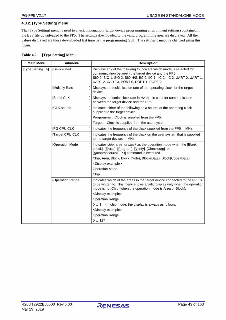
PG-FP5 V2.17 USAGE IN STANDALONE MODE
R20UT2922EJ0500 Rev.5.00 Page 43 of 163 Mar 29, 2019
4.3.2. [Type Setting] menu
The [Type Setting] menu is used to check information (target device programming environment settings) contained in the ESF file downloaded to the FP5. The settings downloaded to the valid programming area are displayed. All the values displayed are those downloaded last time by the programming GUI. The settings cannot be changed using this menu. Table 4.2 [Type Setting] Menu
Main Menu Submenu Description [Type Setting >] [Device Port ] Displays any of the following to indicate which mode is selected for
communication between the target device and the FP5. SIO 0, SIO 1, SIO 2, SIO H/S, IIC 0, IIC 1, IIC 2, IIC 3, UART 0, UART 1, UART 2, UART 3, PORT 0, PORT 1, PORT 2
[Multiply Rate ] Displays the multiplication rate of the operating clock for the target device.
[Serial CLK ] Displays the serial clock rate in Hz that is used for communication between the target device and the FP5.
[CLK source ] Indicates either of the following as a source of the operating clock supplied to the target device. Programmer: Clock is supplied from the FP5. Target: Clock is supplied from the user system.
[PG CPU CLK ] Indicates the frequency of the clock supplied from the FP5 in MHz.
[Target CPU CLK ] Indicates the frequency of the clock on the user system that is supplied to the target device, in MHz.
[Operation Mode ] Indicates chip, area, or block as the operation mode when the [Blank check], [Erase], [Program], [Verify], [Checksum], or [Autoprocedure(E.P.)] command is executed. Chip, Area, Block, Block(Code), Block(Data), Block(Code+Data) <Display example> Operation Mode Chip
[Operation Range ] Indicates which of the areas in the target device connected to the FP5 is to be written to. This menu shows a valid display only when the operation mode is not Chip (when the operation mode is Area or Block). <Display example> Operation Range 0 to 1 *In chip mode, the display is always as follows: <Display example> Operation Range 0 to 127
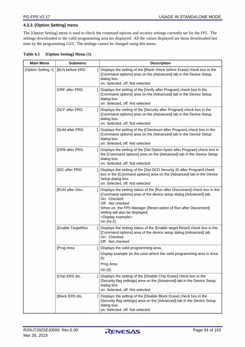
PG-FP5 V2.17 USAGE IN STANDALONE MODE
R20UT2922EJ0500 Rev.5.00 Page 44 of 163 Mar 29, 2019
4.3.3. [Option Setting] menu
The [Option Setting] menu is used to check the command options and security settings currently set for the FP5. The settings downloaded to the valid programming area are displayed. All the values displayed are those downloaded last time by the programming GUI. The settings cannot be changed using this menu. Table 4.3 [Option Setting] Menu (1)
Main Menu Submenu Description [Option Setting >] [BLN before ERS ] Displays the setting of the [Blank check before Erase] check box in the
[Command options] area on the [Advanced] tab in the Device Setup dialog box. on: Selected, off: Not selected
[VRF after PRG ] Displays the setting of the [Verify after Program] check box in the [Command options] area on the [Advanced] tab in the Device Setup dialog box. on: Selected, off: Not selected
[SCF after PRG ] Displays the setting of the [Security after Program] check box in the [Command options] area on the [Advanced] tab in the Device Setup dialog box. on: Selected, off: Not selected
[SUM after PRG ] Displays the setting of the [Checksum after Program] check box in the [Command options] area on the [Advanced] tab in the Device Setup dialog box. on: Selected, off: Not selected
[OPB after PRG ] Displays the setting of the [Set Option bytes after Program] check box in the [Command options] area on the [Advanced] tab in the Device Setup dialog box. on: Selected, off: Not selected
[IDC after PRG ] Displays the setting of the [Set OCD Security ID after Program] check box in the [Command options] area on the [Advanced] tab in the Device Setup dialog box. on: Selected, off: Not selected
[RUN after Disc. ] Displays the setting status of the [Run after Disconnect] check box in the [Command options] area of the device setup dialog [Advanced] tab. On: Checked Off: Not checked When on, the FP5 Manager [Reset option of Run after Disconnect] setting will also be displayed. <Display example> On (Hi-Z)
[Enable TargetRes ] Displays the setting status of the [Enable target Reset] check box in the [Command options] area of the device setup dialog [Advanced] tab. On: Checked Off: Not checked
[Prog Area ] Displays the valid programming area. Display example (in the case where the valid programming area is Area 0): Prog Area On (0)
[Chip ERS dis. ] Displays the setting of the [Disable Chip Erase] check box in the [Security flag settings] area on the [Advanced] tab in the Device Setup dialog box. on: Selected, off: Not selected
[Block ERS dis. ] Displays the setting of the [Disable Block Erase] check box in the [Security flag settings] area on the [Advanced] tab in the Device Setup dialog box. on: Selected, off: Not selected
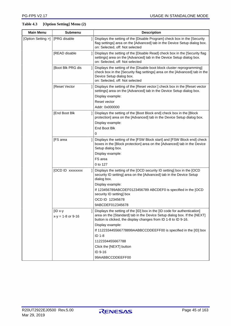
PG-FP5 V2.17 USAGE IN STANDALONE MODE
R20UT2922EJ0500 Rev.5.00 Page 45 of 163 Mar 29, 2019
Table 4.3 [Option Setting] Menu (2)
Main Menu Submenu Description [Option Setting >] [PRG disable ] Displays the setting of the [Disable Program] check box in the [Security
flag settings] area on the [Advanced] tab in the Device Setup dialog box. on: Selected, off: Not selected
[READ disable ] Displays the setting of the [Disable Read] check box in the [Security flag settings] area on the [Advanced] tab in the Device Setup dialog box. on: Selected, off: Not selected
[Boot Blk PRG dis ] Displays the setting of the [Disable boot block cluster reprogramming] check box in the [Security flag settings] area on the [Advanced] tab in the Device Setup dialog box. on: Selected, off: Not selected
[Reset Vector ] Displays the setting of the [Reset vector:] check box in the [Reset vector settings] area on the [Advanced] tab in the Device Setup dialog box. Display example: Reset vector Addr: 0x000000
[End Boot Blk ] Displays the setting of the [Boot Block end] check box in the [Block protection] area on the [Advanced] tab in the Device Setup dialog box. Display example: End Boot Blk 0
[FS area ] Displays the setting of the [FSW Block start] and [FSW Block end] check boxes in the [Block protection] area on the [Advanced] tab in the Device Setup dialog box. Display example: FS area 0 to 127
[OCD ID xxxxxxxx ] Displays the setting of the [OCD security ID setting] box in the [OCD security ID setting] area on the [Advanced] tab in the Device Setup dialog box. Display example: If 123456789ABCDEF0123456789 ABCDEF0 is specified in the [OCD security ID setting] box OCD ID 12345678 9ABCDEF012345678
[ID x-y x-y = 1-8 or 9-16
] Displays the setting of the [ID] box in the [ID code for authentication] area on the [Standard] tab in the Device Setup dialog box. If the [NEXT] button is clicked, the display changes from ID 1-8 to ID 9-16. Display example: If 112233445566778899AABBCCDDEEFF00 is specified in the [ID] box ID 1-8 1122334455667788 Click the [NEXT] button ID 9-16 99AABBCCDDEEFF00
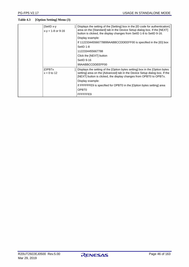
PG-FP5 V2.17 USAGE IN STANDALONE MODE
R20UT2922EJ0500 Rev.5.00 Page 46 of 163 Mar 29, 2019
Table 4.3 [Option Setting] Menu (3)
[SetID x-y x-y = 1-8 or 9-16
] Displays the setting of the [Setting] box in the [ID code for authentication] area on the [Standard] tab in the Device Setup dialog box. If the [NEXT] button is clicked, the display changes from SetID 1-8 to SetID 9-16. Display example: If 112233445566778899AABBCCDDEEFF00 is specified in the [ID] box SetID 1-8 1122334455667788 Click the [NEXT] button SetID 9-16 99AABBCCDDEEFF00
[OPBTx x = 0 to 12
] Displays the setting of the [Option bytes setting] box in the [Option bytes setting] area on the [Advanced] tab in the Device Setup dialog box. If the [NEXT] button is clicked, the display changes from OPBT0 to OPBTx. Display example: If FFFFFFE9 is specified for OPBT0 in the [Option bytes setting] area OPBT0 FFFFFFE9
PG-FP5 V2.17 USAGE IN STANDALONE MODE
R20UT2922EJ0500 Rev.5.00 Page 47 of 163 Mar 29, 2019
4.3.4. [Voltage Setting] menu
The [Voltage Setting] menu is used to check the voltage level setting used when programming the target device currently connected to the FP5. The settings downloaded to the valid programming area are displayed. The settings cannot be changed using this menu. Table 4.4 [Voltage Setting] Menu
Main Menu Submenu Description [Voltage Setting>] [Vdd ] Displays the value of VDD supplied to the target device connected to the
FP5 in volts.
[Vdd2 ] Displays the value of VDD2 supplied to the target device connected to the FP5 in volts.
[Vdd Source ] Indicates the source of VDD supplied from the target device as either of the following. VDD from PG: VDD is supplied from the FP5. VDD from device: VDD is supplied from the user system.
[Vdd Monitoring ] Displays the setting of the [Vdd monitoring] check box in the [Supply voltage] area in the Device Setup dialog box. on: Selected, off: Not selected
[WideVoltage mode ] Displays the setting of the [Wide Voltage Mode] check box.
[FLMD0 Level ] The FLMD0 Level displays the voltage level of the FLMD0 signal.
[CLK Level ] Indicates the voltage level of the clock signal as either of the following. VDD VDD2
[RESET Level ] The Reset Level displays the voltage level of the RESET¯¯¯¯¯¯ signal. VDD Also, when the [Enable target RESET] check box in the [Command options] area of the device setup dialog is enabled, "VDD Reset TrigIn" is displayed.
[Serial Level ] Indicates the voltage level of the serial communication signals. The high level of the serial communication signal is indicated as either of the following. VDD VDD2
[Vpp ] Indicates the value of VPP supplied to the target device connected to the FP5 in volts.
PG-FP5 V2.17 USAGE IN STANDALONE MODE
R20UT2922EJ0500 Rev.5.00 Page 48 of 163 Mar 29, 2019
4.3.5. [Utility/Misc.] menu
The [Utility/Misc.] menu is used to reset the FP5 main unit, tune the LCD contrast, check the firmware version, check the name and version of the PR5 file downloaded, check the name of the program file downloaded, and check the checksum of program files. The settings downloaded to the valid programming area are displayed. The settings cannot be changed using this menu. Table 4.5 [Utility/Misc.] Menu
Main Menu Submenu Description [Utility/Misc. >] [Utility ] Displays the state of the [FP5 Manager] command in the [Programmer]
menu. <Display example> Std. mode Sec: A password has been registered. Std. mode unSec: A password has not been registered.
[Reset FP5 >] Pressing the ENTER button resets the FP5.
[Set LCD Contr. >] Tunes the contrast in the message display. After pressing the ENTER button, the contrast can be tuned using the NEXT (darken) or CANCEL button (lighten). To fix the contrast, click the ENTER button.
[FP5 F/W Version ] Displays the FP5 firmware version. <Display example> FP5 F/W Version V1.00
[PRM Name ] Displays the name of the PR5 file stored in the FP5 valid programming area. <Display example> PRM Name 78F1166
[PRM File Version ] Displays the version of the PR5 file stored in the FP5 valid programming area. <Display example>: PRM File Version V1.00
[HEX File Name ] Displays the name of the program file stored in the FP5 valid programming area. <Display example> HEX File Name Sample.hex “n.a.” is displayed if the program file is invalid.
[File Checksum ] File Checksum will display the results of executing the programming GUI [File] menu -> [Checksum...] command. <Display example> File Checksum 623E (ARITHM.)
PG-FP5 V2.17 USAGE THE REMOTE CONNECTOR
R20UT2922EJ0500 Rev.5.00 Page 49 of 163 Mar 29, 2019
5. USAGE THE REMOTE CONNECTOR This chapter describes the use of the remote connector. The FP5 can be remote controlled by connecting the remote connector and external control device. Remote control can be used to operate and check writing and PASS/ERROR displays from the external control device. 5.1. Remote Interface Mode The remote interface has a standard mode and a bank mode. The modes are switched by using the FP5 Manager [Enable Bank mode] check box. Standard mode: The same signals as the control buttons (NEXT, ENTER, CANCEL) on the command menu of the FP5 unit can be input. Bank mode: This mode allows inputting of the bank signals (BANK0-2) that indicate the programming area. The control buttons (NEXT, ENTER, CANCEL) will change their functions to those inputting bank signals, so that the command menu displayed on the FP5 message display will be disabled. 5.2. Remote Connector Pins The FP5 remote connector pins have the following functions. All inputs will become active with an effective level of 50 ms or greater. Note that the pin numbers in Table 7-1 are the pin numbers on the FP5 remote connector. Table 5.1 Remote Interface Pin Functions
Pin number
Input/ Output
Pin name Function Active level
1 Output CONN Indicates that the remote interface is connected. When the FP5 power is ON, the CONN is always valid.
High level
2 Output BUSY Outputs the status indicated by the status LED “BUSY”. Note that the BUSY signal differs from the status LED and does not blink.
High level
3 Output PASS Outputs the status indicated by the status LED “PASS”. High level
4 Output ERROR Outputs the status indicated by the status LED “ERROR”.
High level
5 Input Standard mode
CANCEL Same as the CANCEL button function. Low level
Input Bank mode BANK0 Indicates the lowest 1 bit of the 3-bit programming area number.
Low level
6 Input Standard mode
ENTER Same function as the ENTER button. Low level
Input Bank mode BANK1 Indicates the middle 1 bit of the 3-bit programming area number.
Low level
7 Input Standard mode
NEXT Same as the function of the NEXT button. Low level
Input Bank mode BANK2 Indicates the highest 1 bit of the 3-bit programming area number.
Low level
8 Input VRF Inputs the independent verify signal. Low level
9 Input START Inputs the “START” (Auto-procedure (E.P.)) signal. Low level
10 Input CLR Clears (disables) the “PASS” and “ERROR” signals. Low level
11 to 15 − GND Grounding pin −
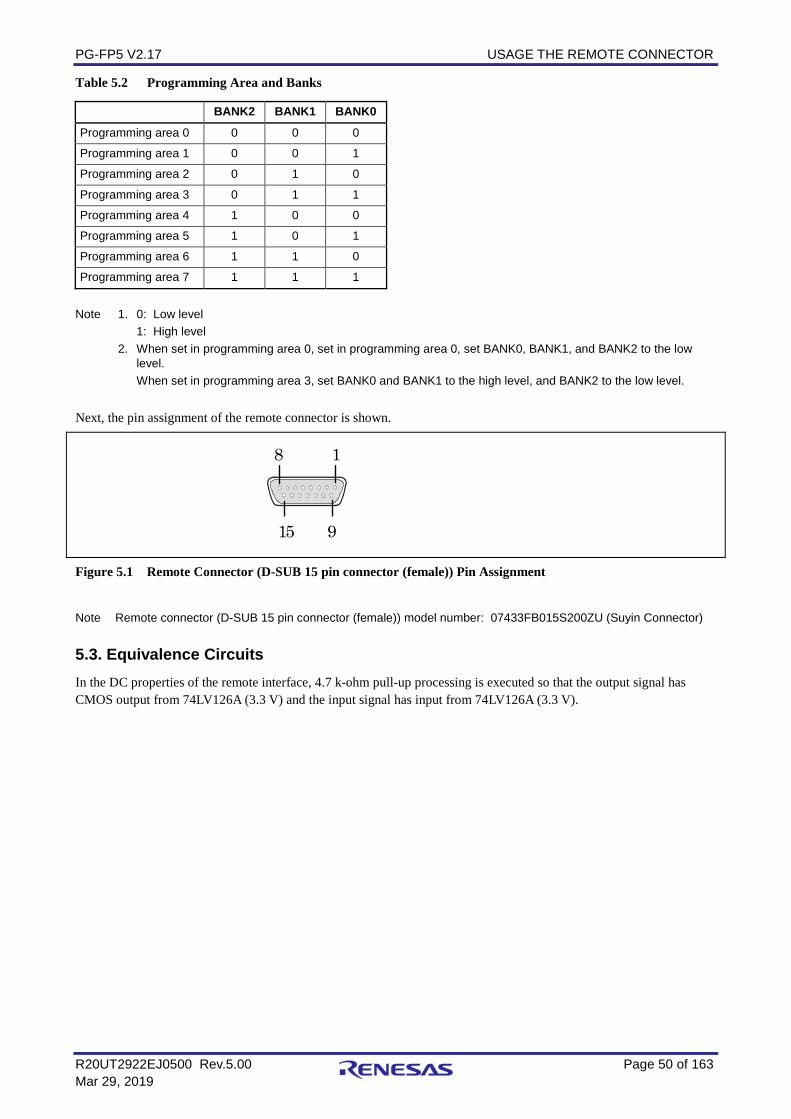
PG-FP5 V2.17 USAGE THE REMOTE CONNECTOR
R20UT2922EJ0500 Rev.5.00 Page 50 of 163 Mar 29, 2019
Table 5.2 Programming Area and Banks
BANK2 BANK1 BANK0 Programming area 0 0 0 0
Programming area 1 0 0 1
Programming area 2 0 1 0
Programming area 3 0 1 1
Programming area 4 1 0 0
Programming area 5 1 0 1
Programming area 6 1 1 0
Programming area 7 1 1 1
Note 1. 0: Low level 1: High level 2. When set in programming area 0, set in programming area 0, set BANK0, BANK1, and BANK2 to the low
level. When set in programming area 3, set BANK0 and BANK1 to the high level, and BANK2 to the low level. Next, the pin assignment of the remote connector is shown.
8 1
15 9
Figure 5.1 Remote Connector (D-SUB 15 pin connector (female)) Pin Assignment
Note Remote connector (D-SUB 15 pin connector (female)) model number: 07433FB015S200ZU (Suyin Connector) 5.3. Equivalence Circuits In the DC properties of the remote interface, 4.7 k-ohm pull-up processing is executed so that the output signal has CMOS output from 74LV126A (3.3 V) and the input signal has input from 74LV126A (3.3 V).
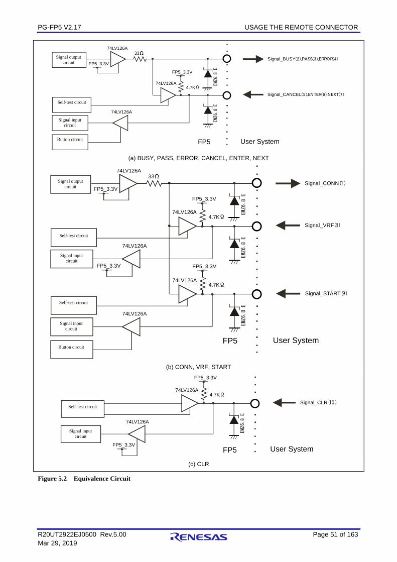
PG-FP5 V2.17 USAGE THE REMOTE CONNECTOR
R20UT2922EJ0500 Rev.5.00 Page 51 of 163 Mar 29, 2019
(a) BUSY, PASS, ERROR, CANCEL, ENTER, NEXT
(b) CONN, VRF, START
(c) CLR
Figure 5.2 Equivalence Circuit
4.7KΩ
FP5
74LV126A
Signal_BUSY(2),PASS(3),ERROR(4)
33
User System
EMZ6.8
E
FP5_3.3V信号出力回路
セルフテスト回路
FP5_3.3V
EMZ6.8
E
Signal_CANCEL(5),ENTER(6),NEXT(7)
信号入力回路
ボタン回路
74LV126A
74LV126A
Signal output circuit
Self-test circuit
Signal input circuit
Button circuit
4.7KΩ
FP5
74LV126A
Signal_CONN33
User System
EMZ6.8E
FP5_3.3V信号出力回路
セルフテスト回路
FP5_3.3V
EMZ6.8E
Signal_VRF
信号入力回路
74LV126A
74LV126A
4.7KΩ
セルフテスト回路
EMZ6.8E
信号入力回路
ボタン回路
74LV126A
FP5_3.3V
74LV126A
Signal_START
FP5_3.3V
Self-test circuit
Signal input circuit
Self-test circuit
Signal input circuit
Button circuit
Signal output circuit
4.7KΩ
FP5 User System
セルフテスト回路
FP5_3.3V
EMZ6.8
E
Signal_CLR
信号入力回路
74LV126A
74LV126A
FP5_3.3V
Self-test circuit
Signal input circuit
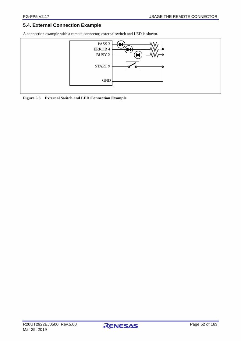
PG-FP5 V2.17 USAGE THE REMOTE CONNECTOR
R20UT2922EJ0500 Rev.5.00 Page 52 of 163 Mar 29, 2019
5.4. External Connection Example A connection example with a remote connector, external switch and LED is shown.
Figure 5.3 External Switch and LED Connection Example
PASS 3 ERROR 4
BUSY 2
START 9
GND
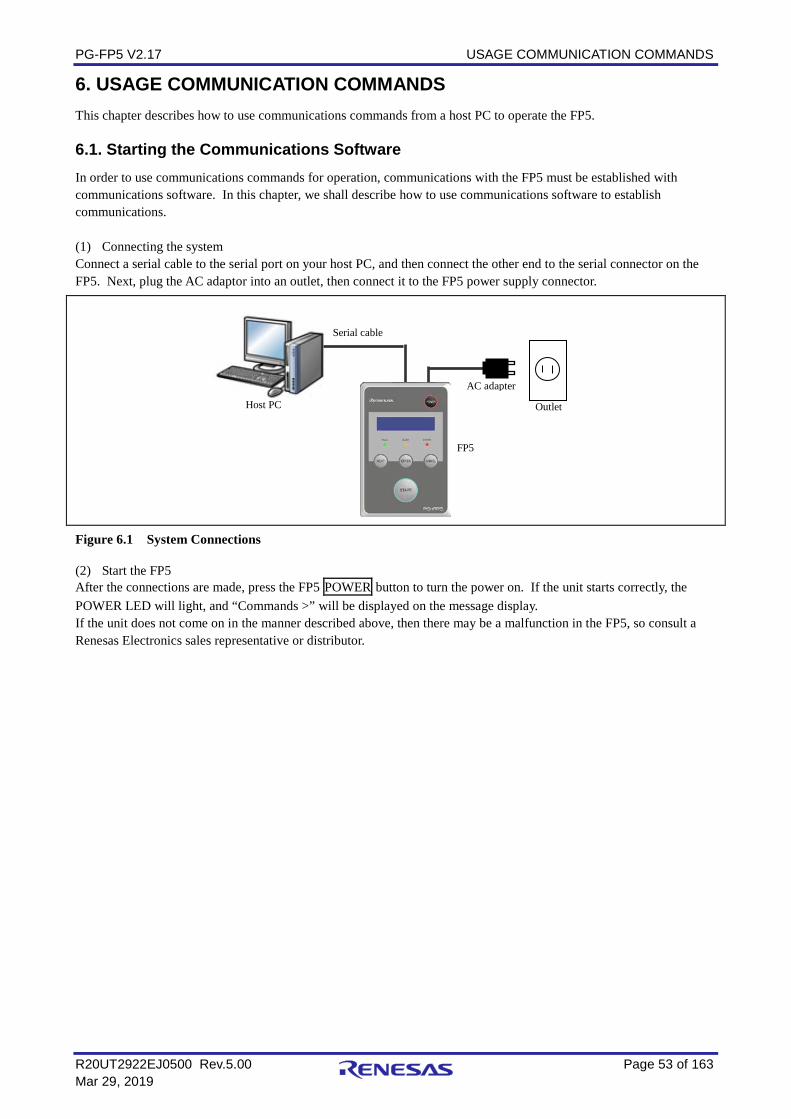
PG-FP5 V2.17 USAGE COMMUNICATION COMMANDS
R20UT2922EJ0500 Rev.5.00 Page 53 of 163 Mar 29, 2019
6. USAGE COMMUNICATION COMMANDS This chapter describes how to use communications commands from a host PC to operate the FP5. 6.1. Starting the Communications Software In order to use communications commands for operation, communications with the FP5 must be established with communications software. In this chapter, we shall describe how to use communications software to establish communications. (1) Connecting the system Connect a serial cable to the serial port on your host PC, and then connect the other end to the serial connector on the FP5. Next, plug the AC adaptor into an outlet, then connect it to the FP5 power supply connector.
Figure 6.1 System Connections
(2) Start the FP5 After the connections are made, press the FP5 POWER button to turn the power on. If the unit starts correctly, the POWER LED will light, and “Commands >” will be displayed on the message display. If the unit does not come on in the manner described above, then there may be a malfunction in the FP5, so consult a Renesas Electronics sales representative or distributor.
Serial cable
AC adapter
Outlet
FP5
Host PC
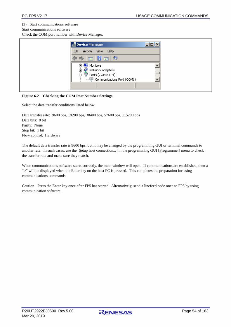
PG-FP5 V2.17 USAGE COMMUNICATION COMMANDS
R20UT2922EJ0500 Rev.5.00 Page 54 of 163 Mar 29, 2019
(3) Start communications software Start communications software Check the COM port number with Device Manager.
Figure 6.2 Checking the COM Port Number Settings
Select the data transfer conditions listed below. Data transfer rate: 9600 bps, 19200 bps, 38400 bps, 57600 bps, 115200 bps Data bits: 8 bit Parity: None Stop bit: 1 bit Flow control: Hardware The default data transfer rate is 9600 bps, but it may be changed by the programming GUI or terminal commands to another rate. In such cases, use the [Setup host connection...] in the programming GUI [Programmer] menu to check the transfer rate and make sure they match. When communications software starts correctly, the main window will open. If communications are established, then a “>” will be displayed when the Enter key on the host PC is pressed. This completes the preparation for using communications commands. Caution Press the Enter key once after FP5 has started. Alternatively, send a linefeed code once to FP5 by using communication software.
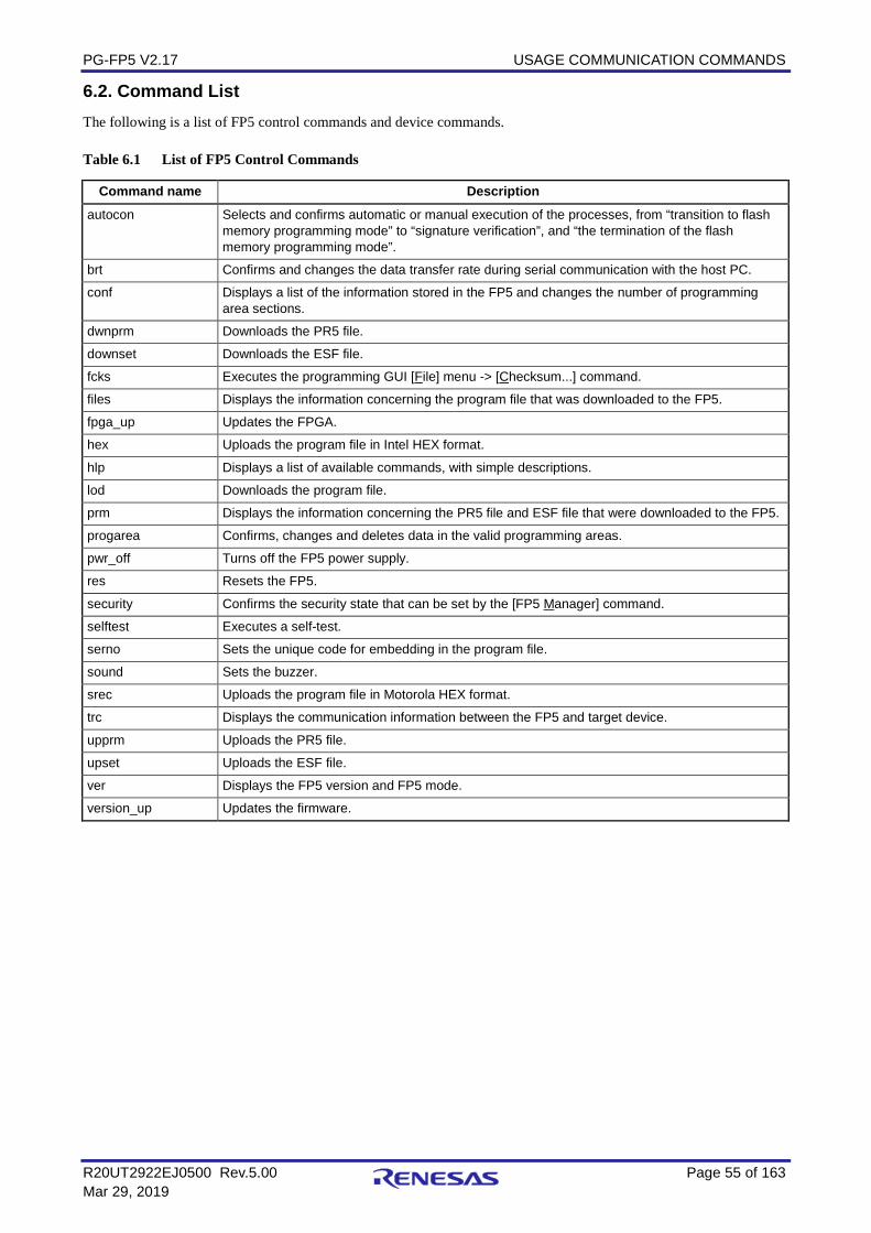
PG-FP5 V2.17 USAGE COMMUNICATION COMMANDS
R20UT2922EJ0500 Rev.5.00 Page 55 of 163 Mar 29, 2019
6.2. Command List The following is a list of FP5 control commands and device commands. Table 6.1 List of FP5 Control Commands
Command name Description autocon Selects and confirms automatic or manual execution of the processes, from “transition to flash
memory programming mode” to “signature verification”, and “the termination of the flash memory programming mode”.
brt Confirms and changes the data transfer rate during serial communication with the host PC.
conf Displays a list of the information stored in the FP5 and changes the number of programming area sections.
dwnprm Downloads the PR5 file.
downset Downloads the ESF file.
fcks Executes the programming GUI [File] menu -> [Checksum...] command.
files Displays the information concerning the program file that was downloaded to the FP5.
fpga_up Updates the FPGA.
hex Uploads the program file in Intel HEX format.
hlp Displays a list of available commands, with simple descriptions.
lod Downloads the program file.
prm Displays the information concerning the PR5 file and ESF file that were downloaded to the FP5.
progarea Confirms, changes and deletes data in the valid programming areas.
pwr_off Turns off the FP5 power supply.
res Resets the FP5.
security Confirms the security state that can be set by the [FP5 Manager] command.
selftest Executes a self-test.
serno Sets the unique code for embedding in the program file.
sound Sets the buzzer.
srec Uploads the program file in Motorola HEX format.
trc Displays the communication information between the FP5 and target device.
upprm Uploads the PR5 file.
upset Uploads the ESF file.
ver Displays the FP5 version and FP5 mode.
version_up Updates the firmware.
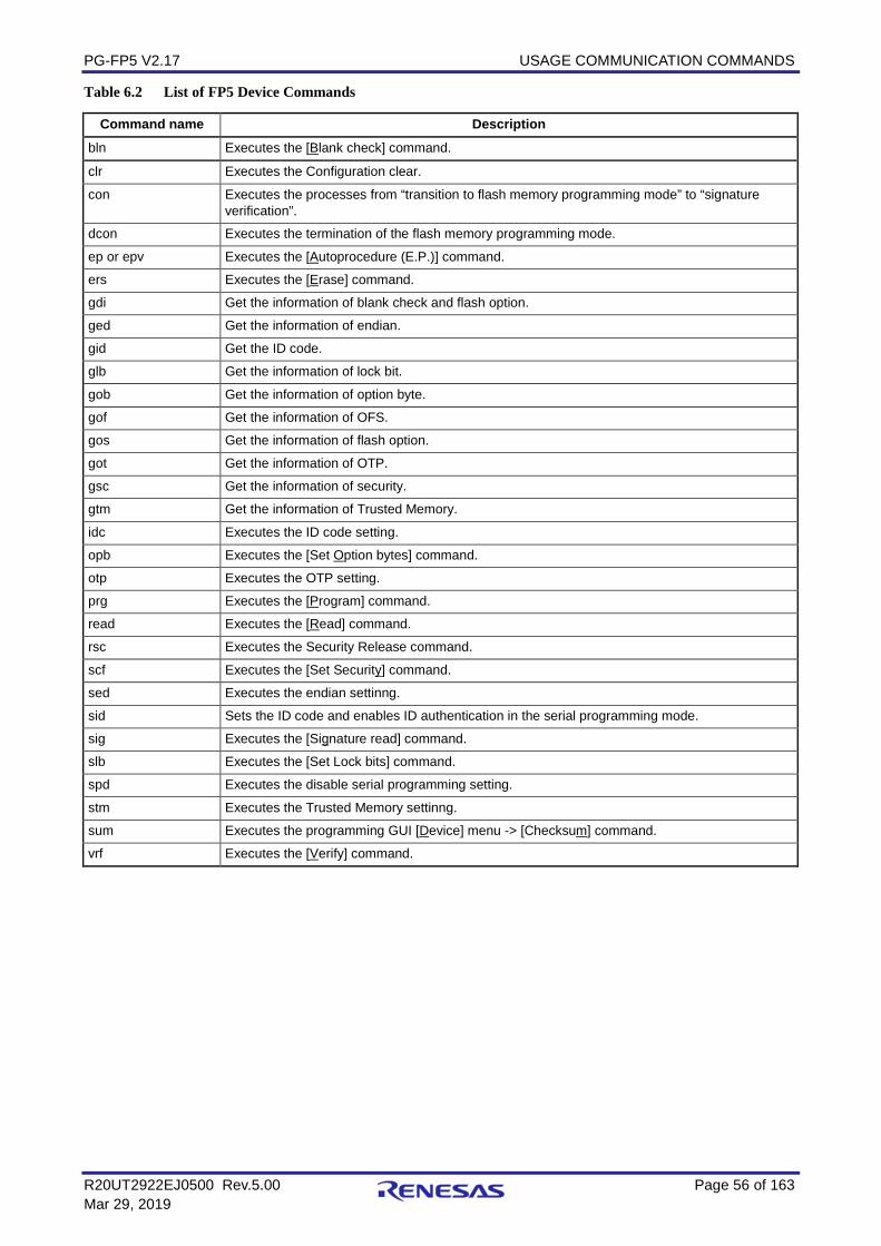
PG-FP5 V2.17 USAGE COMMUNICATION COMMANDS
R20UT2922EJ0500 Rev.5.00 Page 56 of 163 Mar 29, 2019
Table 6.2 List of FP5 Device Commands
Command name Description bln Executes the [Blank check] command.
clr Executes the Configuration clear.
con Executes the processes from “transition to flash memory programming mode” to “signature verification”.
dcon Executes the termination of the flash memory programming mode.
ep or epv Executes the [Autoprocedure (E.P.)] command.
ers Executes the [Erase] command.
gdi Get the information of blank check and flash option.
ged Get the information of endian.
gid Get the ID code.
glb Get the information of lock bit.
gob Get the information of option byte.
gof Get the information of OFS.
gos Get the information of flash option.
got Get the information of OTP.
gsc Get the information of security.
gtm Get the information of Trusted Memory.
idc Executes the ID code setting.
opb Executes the [Set Option bytes] command.
otp Executes the OTP setting.
prg Executes the [Program] command.
read Executes the [Read] command.
rsc Executes the Security Release command.
scf Executes the [Set Security] command.
sed Executes the endian settinng.
sid Sets the ID code and enables ID authentication in the serial programming mode.
sig Executes the [Signature read] command.
slb Executes the [Set Lock bits] command.
spd Executes the disable serial programming setting.
stm Executes the Trusted Memory settinng.
sum Executes the programming GUI [Device] menu -> [Checksum] command.
vrf Executes the [Verify] command.
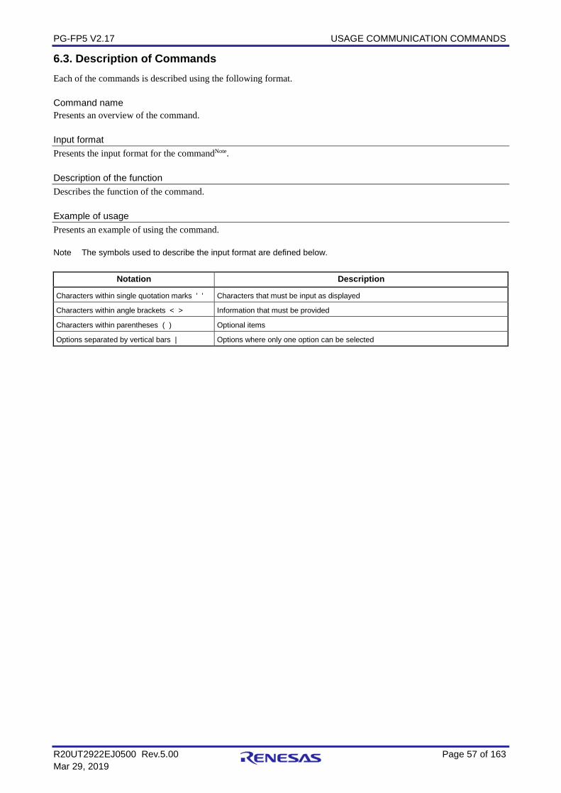
PG-FP5 V2.17 USAGE COMMUNICATION COMMANDS
R20UT2922EJ0500 Rev.5.00 Page 57 of 163 Mar 29, 2019
6.3. Description of Commands Each of the commands is described using the following format. Command name Presents an overview of the command. Input format Presents the input format for the commandNote. Description of the function Describes the function of the command. Example of usage Presents an example of using the command. Note The symbols used to describe the input format are defined below.
Notation Description
Characters within single quotation marks ' ' Characters that must be input as displayed
Characters within angle brackets < > Information that must be provided
Characters within parentheses ( ) Optional items
Options separated by vertical bars | Options where only one option can be selected
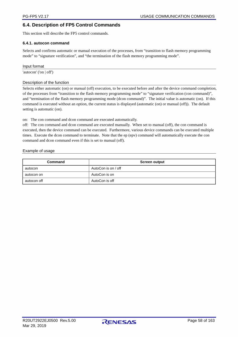
PG-FP5 V2.17 USAGE COMMUNICATION COMMANDS
R20UT2922EJ0500 Rev.5.00 Page 58 of 163 Mar 29, 2019
6.4. Description of FP5 Control Commands This section will describe the FP5 control commands. 6.4.1. autocon command
Selects and confirms automatic or manual execution of the processes, from “transition to flash memory programming mode” to “signature verification”, and “the termination of the flash memory programming mode”. Input format 'autocon' ('on | off') Description of the function Selects either automatic (on) or manual (off) execution, to be executed before and after the device command completion, of the processes from “transition to the flash memory programming mode” to “signature verification (con command)”, and “termination of the flash memory programming mode (dcon command)”. The initial value is automatic (on). If this command is executed without an option, the current status is displayed (automatic (on) or manual (off)). The default setting is automatic (on). on: The con command and dcon command are executed automatically. off: The con command and dcon command are executed manually. When set to manual (off), the con command is executed, then the device command can be executed. Furthermore, various device commands can be executed multiple times. Execute the dcon command to terminate. Note that the ep (epv) command will automatically execute the con command and dcon command even if this is set to manual (off). Example of usage
Command Screen output autocon AutoCon is on / off
autocon on AutoCon is on
autocon off AutoCon is off
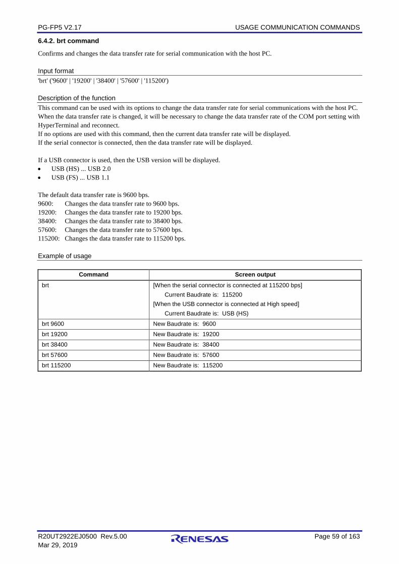
PG-FP5 V2.17 USAGE COMMUNICATION COMMANDS
R20UT2922EJ0500 Rev.5.00 Page 59 of 163 Mar 29, 2019
6.4.2. brt command
Confirms and changes the data transfer rate for serial communication with the host PC. Input format 'brt' ('9600' | '19200' | '38400' | '57600' | '115200') Description of the function This command can be used with its options to change the data transfer rate for serial communications with the host PC. When the data transfer rate is changed, it will be necessary to change the data transfer rate of the COM port setting with HyperTerminal and reconnect. If no options are used with this command, then the current data transfer rate will be displayed. If the serial connector is connected, then the data transfer rate will be displayed. If a USB connector is used, then the USB version will be displayed. • USB (HS) ... USB 2.0 • USB (FS) ... USB 1.1 The default data transfer rate is 9600 bps. 9600: Changes the data transfer rate to 9600 bps. 19200: Changes the data transfer rate to 19200 bps. 38400: Changes the data transfer rate to 38400 bps. 57600: Changes the data transfer rate to 57600 bps. 115200: Changes the data transfer rate to 115200 bps. Example of usage
Command Screen output brt [When the serial connector is connected at 115200 bps]
Current Baudrate is: 115200 [When the USB connector is connected at High speed] Current Baudrate is: USB (HS)
brt 9600 New Baudrate is: 9600
brt 19200 New Baudrate is: 19200
brt 38400 New Baudrate is: 38400
brt 57600 New Baudrate is: 57600
brt 115200 New Baudrate is: 115200
PG-FP5 V2.17 USAGE COMMUNICATION COMMANDS
R20UT2922EJ0500 Rev.5.00 Page 60 of 163 Mar 29, 2019
6.4.3. conf command
Displays a list of the information stored in the FP5 and changes the number of programming area sections. Input format 'conf' ('progarea' '4x4' | '8x2'' | '10/6' | '1x16') Description of the function Divides the programming area into eight, four, two, or one areas depending on the selected option. If an option is not specified, then the following information stored in the FP5 will be displayed. • Version information (firmware version, board hardware version, FPGA version, serial number, FP5 mode) • Program area information (area divisions, valid programming areas, maximum size of program file information (code area, data area)) • Program file information (file name, creation date, size, checksum) • PR5 file and ESF file information in all programming areas (PR5 file names, PR5 file checksums, ESF file checksums) • Automatic connection information • Buzzer information • Automatic power supply OFF information • Security mode information • FP5 manager option setting information Progarea: Used to specify the number of programming area sections. 4x4: Divides the programming area into four sections. 8x2: Divides the programming area into eight sections. 10/6: Divides the programming area into two sections. 1x16: Divides the programming area into one section. Example of usage Refer to the following pages.
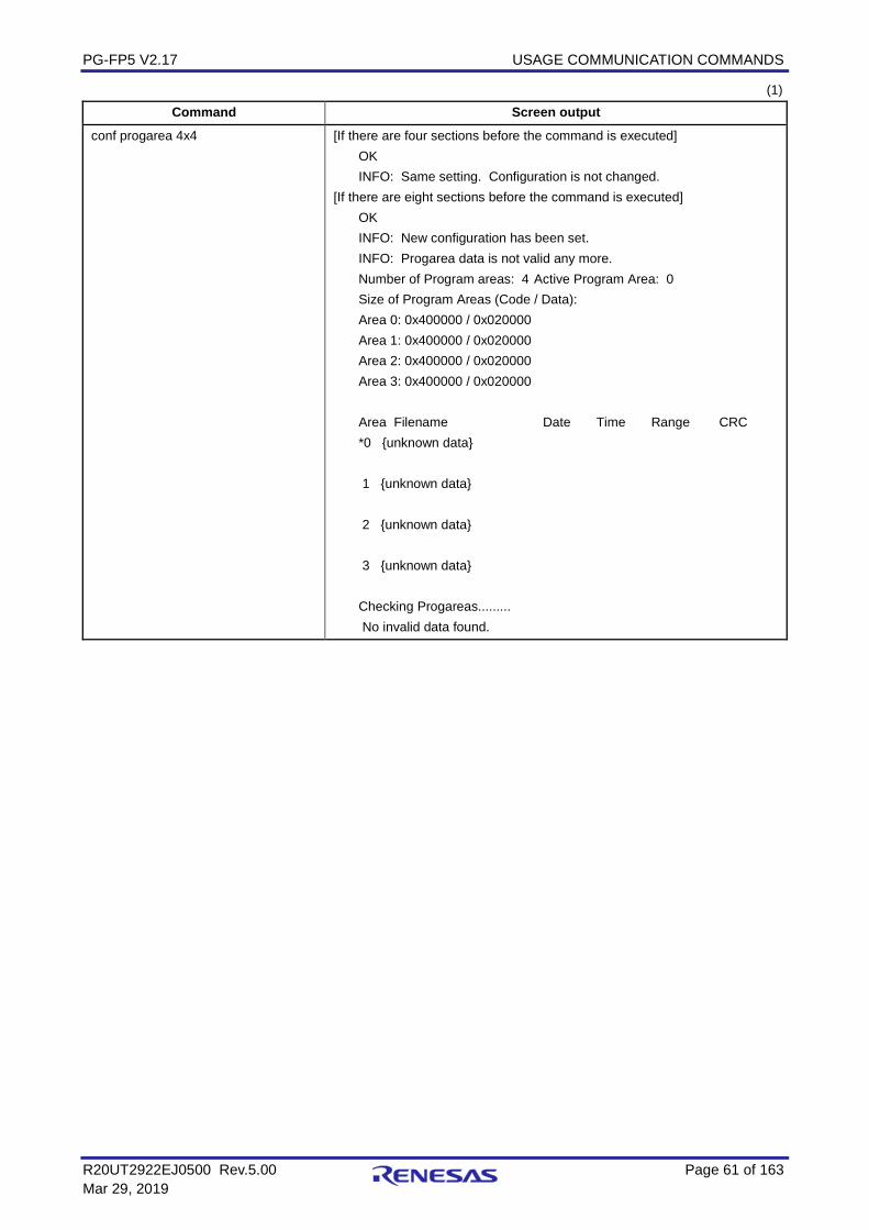
PG-FP5 V2.17 USAGE COMMUNICATION COMMANDS
R20UT2922EJ0500 Rev.5.00 Page 61 of 163 Mar 29, 2019
(1) Command Screen output
conf progarea 4x4 [If there are four sections before the command is executed] OK INFO: Same setting. Configuration is not changed. [If there are eight sections before the command is executed] OK INFO: New configuration has been set. INFO: Progarea data is not valid any more. Number of Program areas: 4 Active Program Area: 0 Size of Program Areas (Code / Data): Area 0: 0x400000 / 0x020000 Area 1: 0x400000 / 0x020000 Area 2: 0x400000 / 0x020000 Area 3: 0x400000 / 0x020000 Area Filename Date Time Range CRC *0 unknown data 1 unknown data 2 unknown data 3 unknown data Checking Progareas......... No invalid data found.
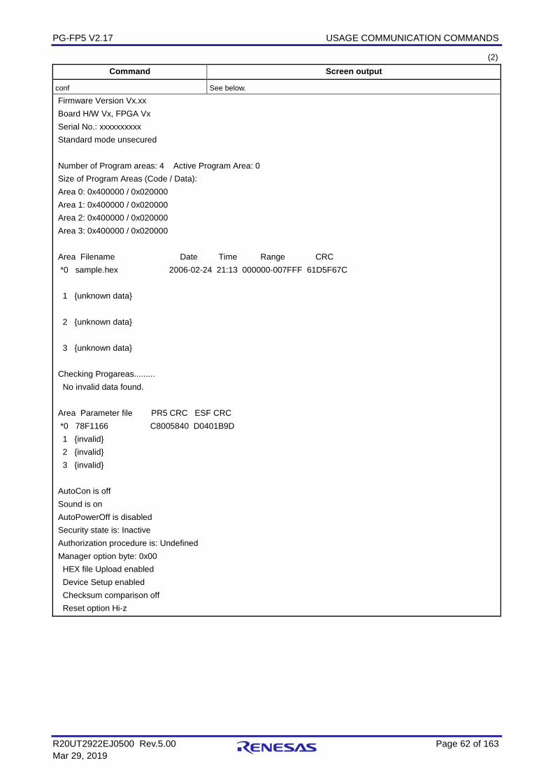
PG-FP5 V2.17 USAGE COMMUNICATION COMMANDS
R20UT2922EJ0500 Rev.5.00 Page 62 of 163 Mar 29, 2019
(2) Command Screen output
conf See below.
Firmware Version Vx.xx Board H/W Vx, FPGA Vx Serial No.: xxxxxxxxxx Standard mode unsecured Number of Program areas: 4 Active Program Area: 0 Size of Program Areas (Code / Data): Area 0: 0x400000 / 0x020000 Area 1: 0x400000 / 0x020000 Area 2: 0x400000 / 0x020000 Area 3: 0x400000 / 0x020000 Area Filename Date Time Range CRC *0 sample.hex 2006-02-24 21:13 000000-007FFF 61D5F67C 1 unknown data 2 unknown data 3 unknown data Checking Progareas......... No invalid data found. Area Parameter file PR5 CRC ESF CRC *0 78F1166 C8005840 D0401B9D 1 invalid 2 invalid 3 invalid AutoCon is off Sound is on AutoPowerOff is disabled Security state is: Inactive Authorization procedure is: Undefined Manager option byte: 0x00 HEX file Upload enabled Device Setup enabled Checksum comparison off Reset option Hi-z
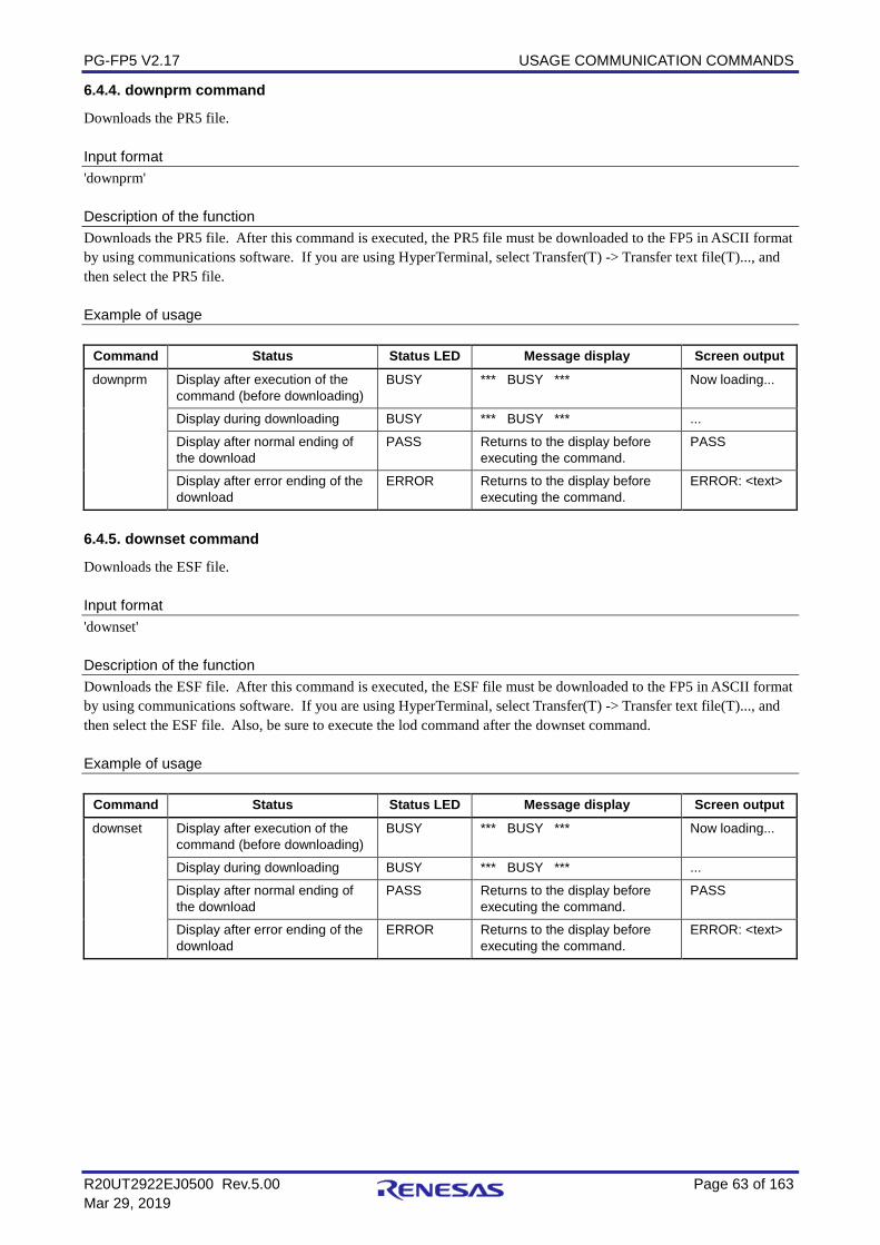
PG-FP5 V2.17 USAGE COMMUNICATION COMMANDS
R20UT2922EJ0500 Rev.5.00 Page 63 of 163 Mar 29, 2019
6.4.4. downprm command
Downloads the PR5 file. Input format 'downprm' Description of the function Downloads the PR5 file. After this command is executed, the PR5 file must be downloaded to the FP5 in ASCII format by using communications software. If you are using HyperTerminal, select Transfer(T) -> Transfer text file(T)..., and then select the PR5 file. Example of usage
Command Status Status LED Message display Screen output downprm Display after execution of the
command (before downloading) BUSY *** BUSY *** Now loading...
Display during downloading BUSY *** BUSY *** ...
Display after normal ending of the download
PASS Returns to the display before executing the command.
PASS
Display after error ending of the download
ERROR Returns to the display before executing the command.
ERROR: <text>
6.4.5. downset command
Downloads the ESF file. Input format 'downset' Description of the function Downloads the ESF file. After this command is executed, the ESF file must be downloaded to the FP5 in ASCII format by using communications software. If you are using HyperTerminal, select Transfer(T) -> Transfer text file(T)..., and then select the ESF file. Also, be sure to execute the lod command after the downset command. Example of usage
Command Status Status LED Message display Screen output downset Display after execution of the
command (before downloading) BUSY *** BUSY *** Now loading...
Display during downloading BUSY *** BUSY *** ...
Display after normal ending of the download
PASS Returns to the display before executing the command.
PASS
Display after error ending of the download
ERROR Returns to the display before executing the command.
ERROR: <text>
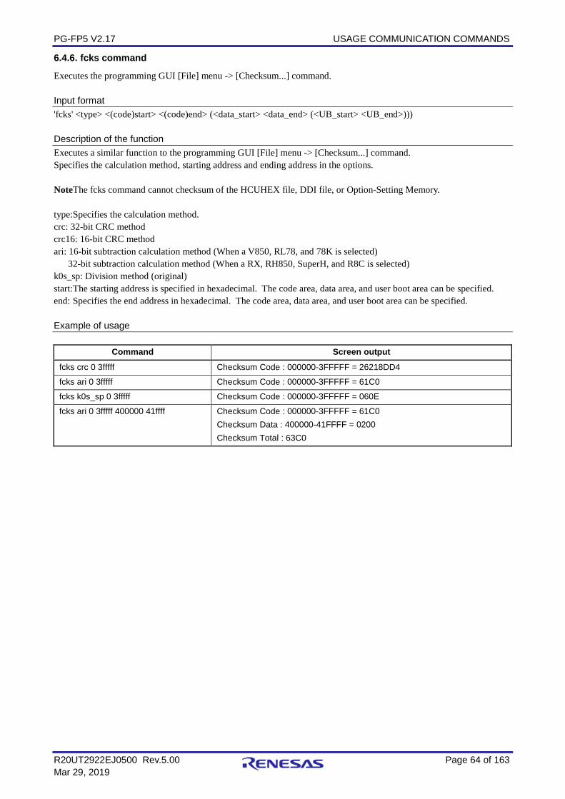
PG-FP5 V2.17 USAGE COMMUNICATION COMMANDS
R20UT2922EJ0500 Rev.5.00 Page 64 of 163 Mar 29, 2019
6.4.6. fcks command
Executes the programming GUI [File] menu -> [Checksum...] command. Input format 'fcks' <type> <(code)start> <(code)end> (<data_start> <data_end> (<UB_start> <UB_end>))) Description of the function Executes a similar function to the programming GUI [File] menu -> [Checksum...] command. Specifies the calculation method, starting address and ending address in the options. NoteThe fcks command cannot checksum of the HCUHEX file, DDI file, or Option-Setting Memory. type:Specifies the calculation method. crc: 32-bit CRC method crc16: 16-bit CRC method ari: 16-bit subtraction calculation method (When a V850, RL78, and 78K is selected)
32-bit subtraction calculation method (When a RX, RH850, SuperH, and R8C is selected) k0s_sp: Division method (original) start:The starting address is specified in hexadecimal. The code area, data area, and user boot area can be specified. end: Specifies the end address in hexadecimal. The code area, data area, and user boot area can be specified. Example of usage
Command Screen output fcks crc 0 3fffff Checksum Code : 000000-3FFFFF = 26218DD4
fcks ari 0 3fffff Checksum Code : 000000-3FFFFF = 61C0
fcks k0s_sp 0 3fffff Checksum Code : 000000-3FFFFF = 060E
fcks ari 0 3fffff 400000 41ffff Checksum Code : 000000-3FFFFF = 61C0 Checksum Data : 400000-41FFFF = 0200 Checksum Total : 63C0
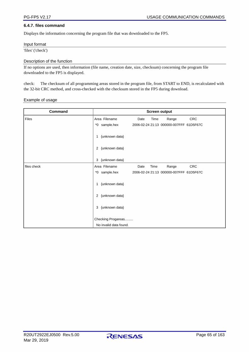
PG-FP5 V2.17 USAGE COMMUNICATION COMMANDS
R20UT2922EJ0500 Rev.5.00 Page 65 of 163 Mar 29, 2019
6.4.7. files command
Displays the information concerning the program file that was downloaded to the FP5. Input format 'files' ('check') Description of the function If no options are used, then information (file name, creation date, size, checksum) concerning the program file downloaded to the FP5 is displayed. check: The checksum of all programming areas stored in the program file, from START to END, is recalculated with the 32-bit CRC method, and cross-checked with the checksum stored in the FP5 during download. Example of usage
Command Screen output
Files Area Filename Date Time Range CRC
*0 sample.hex 2006-02-24 21:13 000000-007FFF 61D5F67C
1 unknown data
2 unknown data
3 unknown data
files check Area Filename Date Time Range CRC
*0 sample.hex 2006-02-24 21:13 000000-007FFF 61D5F67C
1 unknown data
2 unknown data
3 unknown data
Checking Progareas.........
No invalid data found.
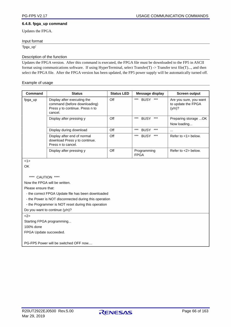
PG-FP5 V2.17 USAGE COMMUNICATION COMMANDS
R20UT2922EJ0500 Rev.5.00 Page 66 of 163 Mar 29, 2019
6.4.8. fpga_up command
Updates the FPGA. Input format 'fpga_up' Description of the function Updates the FPGA version. After this command is executed, the FPGA file must be downloaded to the FP5 in ASCII format using communications software. If using HyperTerminal, select Transfer(T) -> Transfer text file(T)..., and then select the FPGA file. After the FPGA version has been updated, the FP5 power supply will be automatically turned off. Example of usage
Command Status Status LED Message display Screen output fpga_up Display after executing the
command (before downloading) Press y to continue. Press n to cancel.
Off *** BUSY *** Are you sure, you want to update the FPGA (y/n)?
Display after pressing y Off *** BUSY *** Preparing storage ...OK Now loading...
Display during download Off *** BUSY *** ...
Display after end of normal download Press y to continue. Press n to cancel.
Off *** BUSY *** Refer to <1> below.
Display after pressing y Off Programming FPGA
Refer to <2> below.
<1> OK **** CAUTION **** Now the FPGA will be written. Please ensure that: - the correct FPGA Update file has been downloaded - the Power is NOT disconnected during this operation - the Programmer is NOT reset during this operation Do you want to continue (y/n)?
<2> Starting FPGA programming... 100% done FPGA Update succeeded. PG-FP5 Power will be switched OFF now....
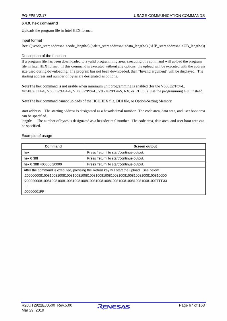
PG-FP5 V2.17 USAGE COMMUNICATION COMMANDS
R20UT2922EJ0500 Rev.5.00 Page 67 of 163 Mar 29, 2019
6.4.9. hex command
Uploads the program file in Intel HEX format. Input format 'hex' ((<code_start address> <code_length>) (<data_start address> <data_length>) (<UB_start address> <UB_length>)) Description of the function If a program file has been downloaded to a valid programming area, executing this command will upload the program file in Intel HEX format. If this command is executed without any options, the upload will be executed with the address size used during downloading. If a program has not been downloaded, then "Invalid argument" will be displayed. The starting address and number of bytes are designated as options. NoteThe hex command is not usable when minimum unit programming is enabled (for the V850E2/Fx4-L, V850E2/FF4-G, V850E2/FG4-G, V850E2/Px4-L, V850E2/PG4-S, RX, or RH850). Use the programming GUI instead. NoteThe hex command cannot uploads of the HCUHEX file, DDI file, or Option-Setting Memory. start address: The starting address is designated as a hexadecimal number. The code area, data area, and user boot area can be specified. length: The number of bytes is designated as a hexadecimal number. The code area, data area, and user boot area can be specified. Example of usage
Command Screen output hex Press 'return' to start/continue output.
hex 0 3fff Press 'return' to start/continue output.
hex 0 3ffff 400000 20000 Press 'return' to start/continue output.
After the command is executed, pressing the Return key will start the upload. See below. :200000008100810081008100810081008100810081008100810081008100810081008100D0 :20002000810081008100810081008100810081008100810081008100810081008100FFFF33 : :00000001FF
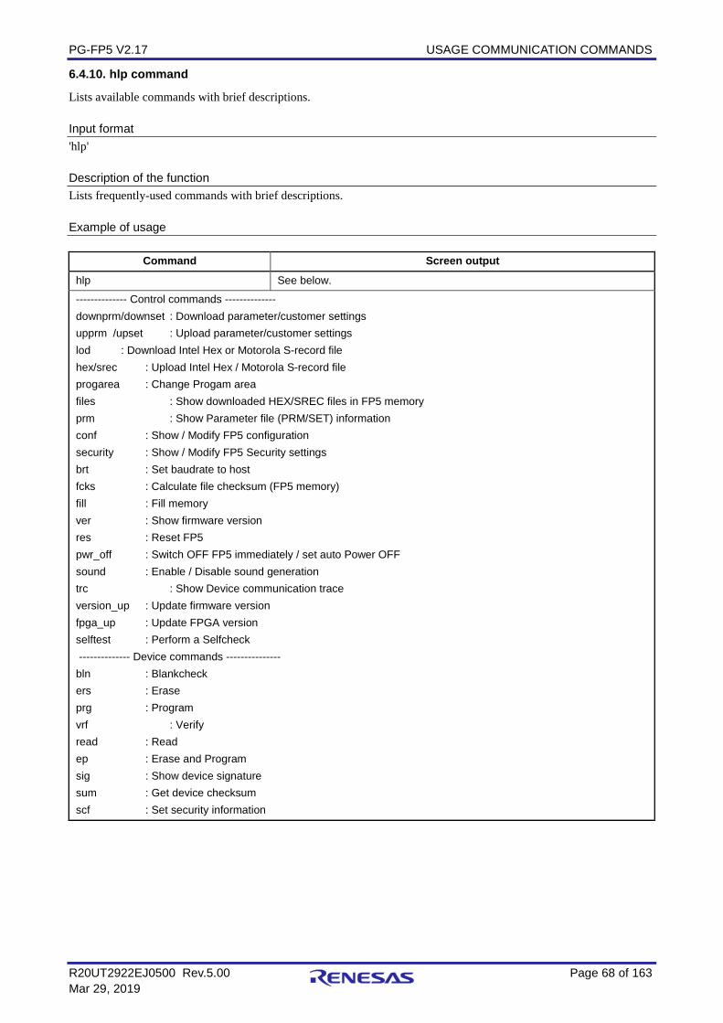
PG-FP5 V2.17 USAGE COMMUNICATION COMMANDS
R20UT2922EJ0500 Rev.5.00 Page 68 of 163 Mar 29, 2019
6.4.10. hlp command
Lists available commands with brief descriptions. Input format 'hlp' Description of the function Lists frequently-used commands with brief descriptions. Example of usage
Command Screen output hlp See below.
-------------- Control commands -------------- downprm/downset : Download parameter/customer settings upprm /upset : Upload parameter/customer settings lod : Download Intel Hex or Motorola S-record file hex/srec : Upload Intel Hex / Motorola S-record file progarea : Change Progam area files : Show downloaded HEX/SREC files in FP5 memory prm : Show Parameter file (PRM/SET) information conf : Show / Modify FP5 configuration security : Show / Modify FP5 Security settings brt : Set baudrate to host fcks : Calculate file checksum (FP5 memory) fill : Fill memory ver : Show firmware version res : Reset FP5 pwr_off : Switch OFF FP5 immediately / set auto Power OFF sound : Enable / Disable sound generation trc : Show Device communication trace version_up : Update firmware version fpga_up : Update FPGA version selftest : Perform a Selfcheck -------------- Device commands --------------- bln : Blankcheck ers : Erase prg : Program vrf : Verify read : Read ep : Erase and Program sig : Show device signature sum : Get device checksum scf : Set security information
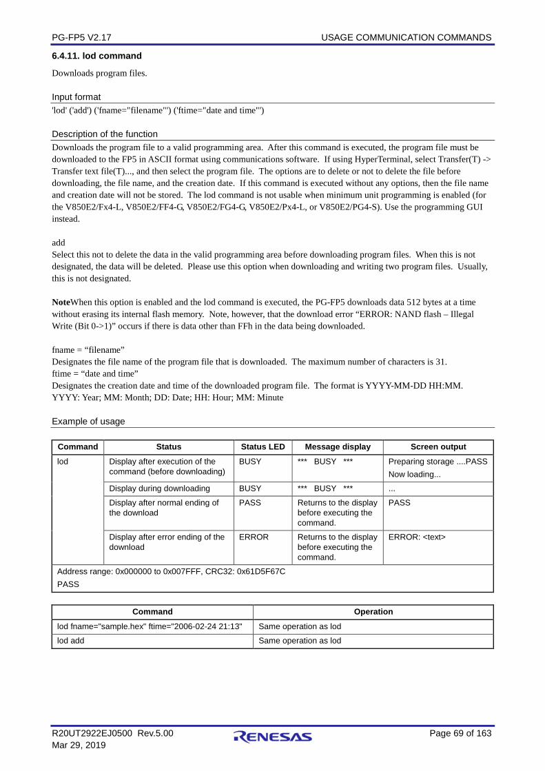
PG-FP5 V2.17 USAGE COMMUNICATION COMMANDS
R20UT2922EJ0500 Rev.5.00 Page 69 of 163 Mar 29, 2019
6.4.11. lod command
Downloads program files. Input format 'lod' ('add') ('fname="filename"') ('ftime="date and time"') Description of the function Downloads the program file to a valid programming area. After this command is executed, the program file must be downloaded to the FP5 in ASCII format using communications software. If using HyperTerminal, select Transfer(T) -> Transfer text file(T)..., and then select the program file. The options are to delete or not to delete the file before downloading, the file name, and the creation date. If this command is executed without any options, then the file name and creation date will not be stored. The lod command is not usable when minimum unit programming is enabled (for the V850E2/Fx4-L, V850E2/FF4-G, V850E2/FG4-G, V850E2/Px4-L, or V850E2/PG4-S). Use the programming GUI instead. add Select this not to delete the data in the valid programming area before downloading program files. When this is not designated, the data will be deleted. Please use this option when downloading and writing two program files. Usually, this is not designated. NoteWhen this option is enabled and the lod command is executed, the PG-FP5 downloads data 512 bytes at a time without erasing its internal flash memory. Note, however, that the download error “ERROR: NAND flash – Illegal Write (Bit 0->1)” occurs if there is data other than FFh in the data being downloaded. fname = “filename” Designates the file name of the program file that is downloaded. The maximum number of characters is 31. ftime = “date and time” Designates the creation date and time of the downloaded program file. The format is YYYY-MM-DD HH:MM. YYYY: Year; MM: Month; DD: Date; HH: Hour; MM: Minute Example of usage
Command Status Status LED Message display Screen output lod Display after execution of the
command (before downloading) BUSY *** BUSY *** Preparing storage ....PASS
Now loading...
Display during downloading BUSY *** BUSY *** ...
Display after normal ending of the download
PASS Returns to the display before executing the command.
PASS
Display after error ending of the download
ERROR Returns to the display before executing the command.
ERROR: <text>
Address range: 0x000000 to 0x007FFF, CRC32: 0x61D5F67C PASS
Command Operation
lod fname="sample.hex" ftime="2006-02-24 21:13" Same operation as lod
lod add Same operation as lod
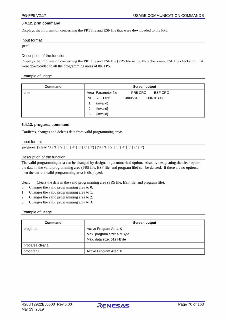
PG-FP5 V2.17 USAGE COMMUNICATION COMMANDS
R20UT2922EJ0500 Rev.5.00 Page 70 of 163 Mar 29, 2019
6.4.12. prm command
Displays the information concerning the PR5 file and ESF file that were downloaded to the FP5. Input format 'prm' Description of the function Displays the information concerning the PR5 file and ESF file (PR5 file name, PR5 checksum, ESF file checksum) that were downloaded to all the programming areas of the FP5. Example of usage
Command Screen output prm Area Parameter file PR5 CRC ESF CRC
*0 78F1166 C8005840 D0401B9D 1 invalid 2 invalid 3 invalid
6.4.13. progarea command
Confirms, changes and deletes data from valid programming areas. Input format 'progarea' ('clear' '0' | '1' | '2' | '3' | '4' | '5' | '6' | '7') | ('0' | '1' | '2' | '3' | '4' | '5' | '6' | '7') Description of the function The valid programming area can be changed by designating a numerical option. Also, by designating the clear option, the data in the valid programming area (PR5 file, ESF file, and program file) can be deleted. If there are no options, then the current valid programming area is displayed. clear: Clears the data in the valid programming area (PR5 file, ESF file, and program file). 0: Changes the valid programming area to 0. 1: Changes the valid programming area to 1. 2: Changes the valid programming area to 2. 3: Changes the valid programming area to 3. Example of usage
Command Screen output progarea Active Program Area: 0
Max. program size: 4 MByte Max. data size: 512 kByte
progarea clear 1
progarea 0 Active Program Area: 0
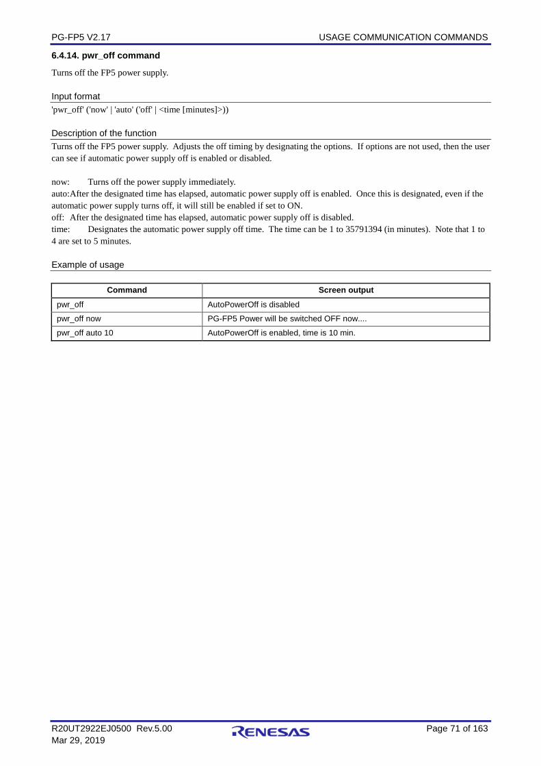
PG-FP5 V2.17 USAGE COMMUNICATION COMMANDS
R20UT2922EJ0500 Rev.5.00 Page 71 of 163 Mar 29, 2019
6.4.14. pwr_off command
Turns off the FP5 power supply. Input format 'pwr_off' ('now' | 'auto' ('off' | <time [minutes]>)) Description of the function Turns off the FP5 power supply. Adjusts the off timing by designating the options. If options are not used, then the user can see if automatic power supply off is enabled or disabled. now: Turns off the power supply immediately. auto:After the designated time has elapsed, automatic power supply off is enabled. Once this is designated, even if the automatic power supply turns off, it will still be enabled if set to ON. off: After the designated time has elapsed, automatic power supply off is disabled. time: Designates the automatic power supply off time. The time can be 1 to 35791394 (in minutes). Note that 1 to 4 are set to 5 minutes. Example of usage
Command Screen output pwr_off AutoPowerOff is disabled
pwr_off now PG-FP5 Power will be switched OFF now....
pwr_off auto 10 AutoPowerOff is enabled, time is 10 min.
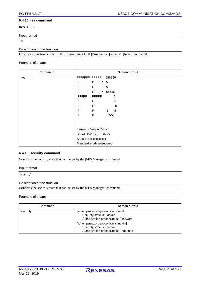
PG-FP5 V2.17 USAGE COMMUNICATION COMMANDS
R20UT2922EJ0500 Rev.5.00 Page 72 of 163 Mar 29, 2019
6.4.15. res command
Resets FP5. Input format 'res' Description of the function Executes a function similar to the programming GUI [Programmer] menu -> [Reset] command. Example of usage
Command Screen output res FFFFFFF PPPPP 555555
F P P 5 F P P 5 F P P 55555 FFFFF PPPPP 5 F P 5 F P 5 F P 5 5 F P 5555 Firmware Version Vx.xx Board H/W Vx, FPGA Vx Serial No.:xxxxxxxxxx Standard mode unsecured
6.4.16. security command
Confirms the security state that can be set by the [FP5 Manager] command. Input format
'security' Description of the function Confirms the security state that can be set by the [FP5 Manager] command. Example of usage
Command Screen output security [When password-protection is valid]
Security state is: Locked Authorization procedure is: Password [When password-protection is invalid] Security state is: Inactive Authorization procedure is: Undefined
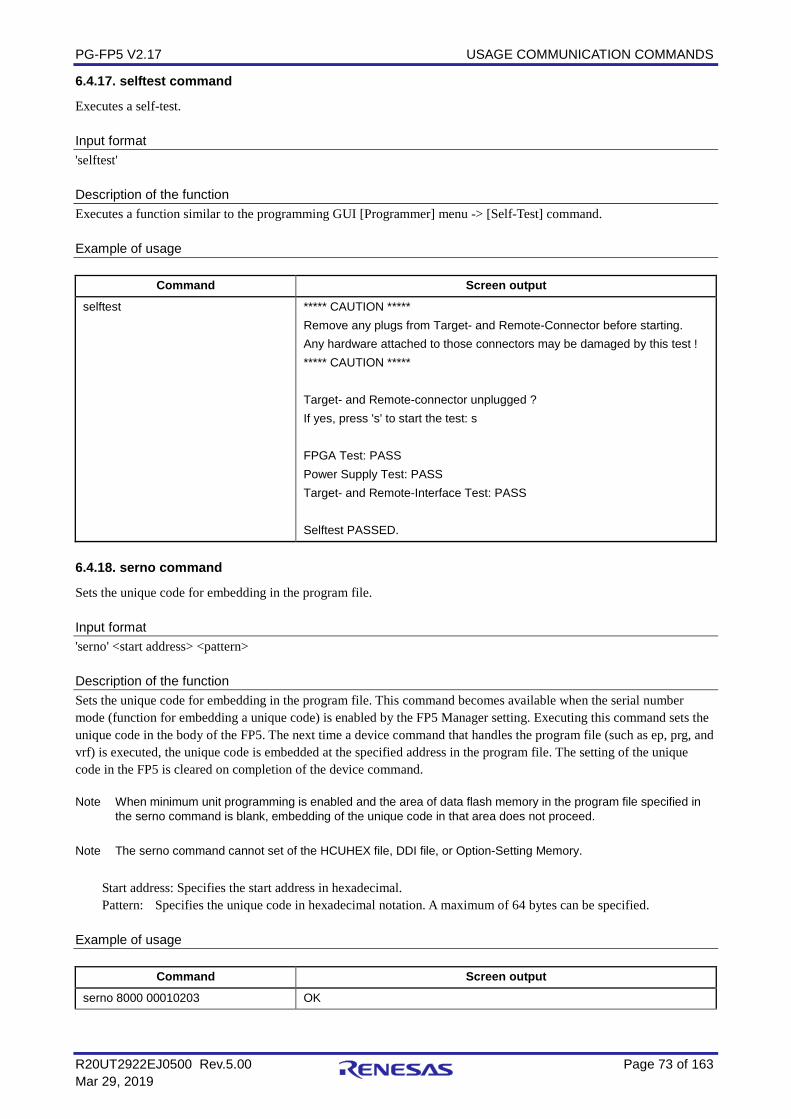
PG-FP5 V2.17 USAGE COMMUNICATION COMMANDS
R20UT2922EJ0500 Rev.5.00 Page 73 of 163 Mar 29, 2019
6.4.17. selftest command
Executes a self-test. Input format 'selftest' Description of the function Executes a function similar to the programming GUI [Programmer] menu -> [Self-Test] command. Example of usage
Command Screen output selftest ***** CAUTION *****
Remove any plugs from Target- and Remote-Connector before starting. Any hardware attached to those connectors may be damaged by this test ! ***** CAUTION ***** Target- and Remote-connector unplugged ? If yes, press 's' to start the test: s FPGA Test: PASS Power Supply Test: PASS Target- and Remote-Interface Test: PASS Selftest PASSED.
6.4.18. serno command
Sets the unique code for embedding in the program file. Input format 'serno' <start address> <pattern> Description of the function Sets the unique code for embedding in the program file. This command becomes available when the serial number mode (function for embedding a unique code) is enabled by the FP5 Manager setting. Executing this command sets the unique code in the body of the FP5. The next time a device command that handles the program file (such as ep, prg, and vrf) is executed, the unique code is embedded at the specified address in the program file. The setting of the unique code in the FP5 is cleared on completion of the device command. Note When minimum unit programming is enabled and the area of data flash memory in the program file specified in
the serno command is blank, embedding of the unique code in that area does not proceed. Note The serno command cannot set of the HCUHEX file, DDI file, or Option-Setting Memory. Start address: Specifies the start address in hexadecimal. Pattern: Specifies the unique code in hexadecimal notation. A maximum of 64 bytes can be specified. Example of usage
Command Screen output serno 8000 00010203 OK
PG-FP5 V2.17 USAGE COMMUNICATION COMMANDS
R20UT2922EJ0500 Rev.5.00 Page 74 of 163 Mar 29, 2019
6.4.19. sound command
Sets the buzzer. Input format 'sound' ('off' | 'on') Description of the function Sets the buzzer. “Enabled” or “disabled” is optionally designated. If no option is designated, the current setting is displayed. off: Disables the buzzer. on: Enables the buzzer. Example of usage
Command Screen output sound Sound is on
sound off Sound is off
PG-FP5 V2.17 USAGE COMMUNICATION COMMANDS
R20UT2922EJ0500 Rev.5.00 Page 75 of 163 Mar 29, 2019
6.4.20. srec command
Uploads the program file in Motorola HEX format. Input format 'srec' ((<code_start address> <code_length>) (<data_start address> <data_length>) (<UB_start address> <UB_length>)) Description of the function If a program file has been downloaded to a valid programming area, executing this command will upload the program file in Motorola HEX format. If this command is executed without any options, the upload will be executed with the address size used during downloading. If a program has not been downloaded, then "Invalid argument" will be displayed. The starting address and number of bytes are designated as options. NoteThe srec command is not usable when minimum unit programming is enabled (for the V850E2/Fx4-L, V850E2/FF4-G, V850E2/FG4-G, V850E2/Px4-L, V850E2/PG4-S, RX, or RH850). Use the programming GUI instead. NoteThe srec command cannot uploads of the HCUHEX file, DDI file, or Option-Setting Memory. start address: The starting address is designated as a hexadecimal number. The code area, data area, and user boot area can be specified. length: The number of bytes is designated as a hexadecimal number. The code area, data area, and user boot area can be specified. Example of usage
Command Screen output srec Press 'return' to start/continue output.
srec 0 3fff Press 'return' to start/continue output.
srec 0 3ffff 400000 20000 Press 'return' to start/continue output.
After the command is executed, pressing the Return key will start the upload. S0030000FC S325000000008100810081008100810081008100810081008100810081008100810081008100CA S32500000020810081008100810081008100810081008100810081008100810081008100FFFF2D : S5030000FC S70500000000FA
PG-FP5 V2.17 USAGE COMMUNICATION COMMANDS
R20UT2922EJ0500 Rev.5.00 Page 76 of 163 Mar 29, 2019
6.4.21. trc command
Displays the communication information between the FP5 and target device. Input format 'trc' Description of the function Displays the communication information between the FP5 and target device stored in the FP5 trace memory. Up to 1024 lines can be stored. The FP5 has ring structure trace memory. Example of usage
Command Screen output trc See below.
Debug Output Number Time us Send Rec. : 0214 0008675924 17 -- 0215 0008678930 -- 02 : Total number of transmitted bytes : 266282 Total number of received bytes : 006212
6.4.22. upprm command
Uploads the PR5 file. Input format 'upprm' Description of the function If the PR5 file has been downloaded to a valid programming area, then executing this command will upload the PR5 file. Example of usage
Command Screen output upprm Press 'return' to start/continue output.
After the command is executed, pressing the Return key will start the upload. [FlashProParameterFile] : [CHECKSUM] SUM=BA9F0491 [EOF]
PG-FP5 V2.17 USAGE COMMUNICATION COMMANDS
R20UT2922EJ0500 Rev.5.00 Page 77 of 163 Mar 29, 2019
6.4.23. upset command
Uploads the ESF file. Input format 'upset' Description of the function If the ESF file has been downloaded to a valid programming area, then executing this command will upload the ESF file. Example of usage
Command Screen output upset Press 'return' to start/continue output.
After the command is executed, pressing the Return key will start the upload. [FlashproCustomerSettingFile] : [CHECKSUM] SUM=F7D4A9E7 [EOF]
6.4.24. ver command
Displays the FP5 version. Input format 'ver' Description of the function Displays the FP5 version (firmware version, board hardware version, FPGA version, and serial number). Example of usage
Command Screen output ver Firmware Version Vx.xx
Board H/W Vx, FPGA Vx Serial No.:xxxxxxxxxx Standard mode unsecured
PG-FP5 V2.17 USAGE COMMUNICATION COMMANDS
R20UT2922EJ0500 Rev.5.00 Page 78 of 163 Mar 29, 2019
6.4.25. version_up command
Updates the firmware. Input format 'version_up' Description of the function Upgrades the firmware. After this command is executed, the firmware file must be downloaded to the FP5 in ASCII format using communications software. If using HyperTerminal, select Transfer(T) -> Transfer text file(T)..., and then select the firmware file. After the firmware version has been updated, the FP5 will be reset. Example of usage Refer to the following pages.
Command Status Status LED Message display Screen output version_up Display after executing
the command (before downloading) Press y to continue. Press n to cancel.
Off *** BUSY *** Are you sure, you want to update the Firmware (y/n)?
Display after pressing y Off *** BUSY *** Preparing storage ...OK Now loading...
Display during download Off *** BUSY *** ...
Display after end of normal download Press y to continue. Press n to cancel.
Off *** BUSY *** Refer to <1> below.
Display after pressing y Off Selfprogramming Firmware
Refer to <2> below.
<1> OK **** CAUTION **** Now the Firmware will be written. Please ensure that: - the correct Firmware Update file has been downloaded - the Power is NOT disconnected during this operation - the Programmer is NOT reset during this operation Do you want to continue (y/n)?
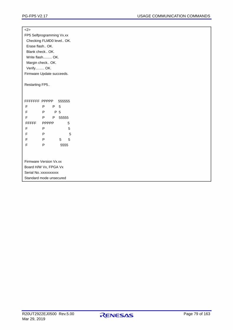
PG-FP5 V2.17 USAGE COMMUNICATION COMMANDS
R20UT2922EJ0500 Rev.5.00 Page 79 of 163 Mar 29, 2019
<2> FP5 Selfprogramming Vx.xx Checking FLMD0 level.. OK. Erase flash.. OK. Blank check.. OK. Write flash......... OK. Margin check.. OK. Verify......... OK. Firmware Update succeeds. Restarting FP5.. FFFFFFF PPPPP 555555 F P P 5 F P P 5 F P P 55555 FFFFF PPPPP 5 F P 5 F P 5 F P 5 5 F P 5555 Firmware Version Vx.xx Board H/W Vx, FPGA Vx Serial No.:xxxxxxxxxx Standard mode unsecured
PG-FP5 V2.17 USAGE COMMUNICATION COMMANDS
R20UT2922EJ0500 Rev.5.00 Page 80 of 163 Mar 29, 2019
6.5. Description of The FP5 Device Commands This section describes the FP5 device commands. 6.5.1. bln command
Executes [Blank check] command. Input format 'bln' Description of the function Executes a similar function to the programming GUI [Device] menu -> [Blank check] command. Example of usage
Command Status Status LED Message display Screen output bln Display while executing the
command [Chip mode] BUSY Blank chk. Chip
... Blank check User area: ERROR Blank check User Boot area: Blank check Data area:
Display while executing the command [Block mode]
BUSY Blank chk. Block ...
Display while executing the command [Area mode]
BUSY Blank chk. Area ...
Display after executing the command [For blank devices]
PASS Returns to the display before executing the command.
PASS Blank check operation finished.
Display after executing the command [For not blank devices]
ERROR ERROR: 051 Blank chk failed
ERROR(E051): Not Blank. Blank check operation finished.
6.5.2. clr command
Executes the Configuration clear. Input format 'clr' Description of the function Executes the Configuration clear. Example of usage
Command Status Status LED Message display Screen output clr Display after executing the
command [When completed normally]
PASS Returns to the display before executing the command.
Configuration clear : PASS Configuration clear operation finished.
Display after executing the command [When terminated abnormally]
ERROR ERROR: xxx xxxxxxxxxxxxxxxx
ERROR(Exxx): <text>
PG-FP5 V2.17 USAGE COMMUNICATION COMMANDS
R20UT2922EJ0500 Rev.5.00 Page 81 of 163 Mar 29, 2019
6.5.3. con command
Executes the processes from “transition to the flash memory programming mode” to “signature verification”. Input format 'con' Description of the function Executes the processes from “transition to the flash memory programming mode” to “signature verification”. In order to use this command, “manual” (off) must be set with the autocon command beforehand. Example of usage
Command Status Status LED Message display Screen output con Display while executing the
command BUSY Connecting:
Display after executing the command [When completed normally]
PASS Returns to the display before executing the command.
PASS Dxxxxxxx>
Display after executing the command [When terminated abnormally]
ERROR ERROR: xxx xxxxxxxxxxxxxxxx
ERROR(Exxx): <text>
6.5.4. dcon command
Executes the process to end the flash memory programming mode. Input format 'dcon' Description of the function Executes the process to end the flash memory programming mode. In order to use this command, "manual" (off) must be set with the autocon command beforehand. Example of usage
Command Status Status LED Message display Screen output con Display while executing the
command BUSY Disconnecting:
Display after executing the command
PASS Returns to the display before executing the command.
Device disconnected.
PG-FP5 V2.17 USAGE COMMUNICATION COMMANDS
R20UT2922EJ0500 Rev.5.00 Page 82 of 163 Mar 29, 2019
6.5.5. ep/epv command
Executes [Autoprocedure(E.P.)] command. Input format 'ep' or 'epv' Description of the function Executes a similar function to the programming GUI [Device] menu -> [Autoprocedure(E.P.)] command. Example of usage
Command Status Status LED Message display Screen output ep or epv
Display while executing the command
BUSY Blank check Skipped. Erase Chip: PASS Program Chip: 10% 20% : 100%
Display after executing the command [When completed normally]
PASS Returns to the display before executing the command.
PASS Erase,Program operation finished. or PASS EPV operation finished.
Display after executing the command [When terminated abnormally]
ERROR ERROR: xxx xxxxxxxxxxxxxxxx
ERROR(Exxx): <text> Erase,Program operation finished. or ERROR(Exxx): <text> EPV operation finished.
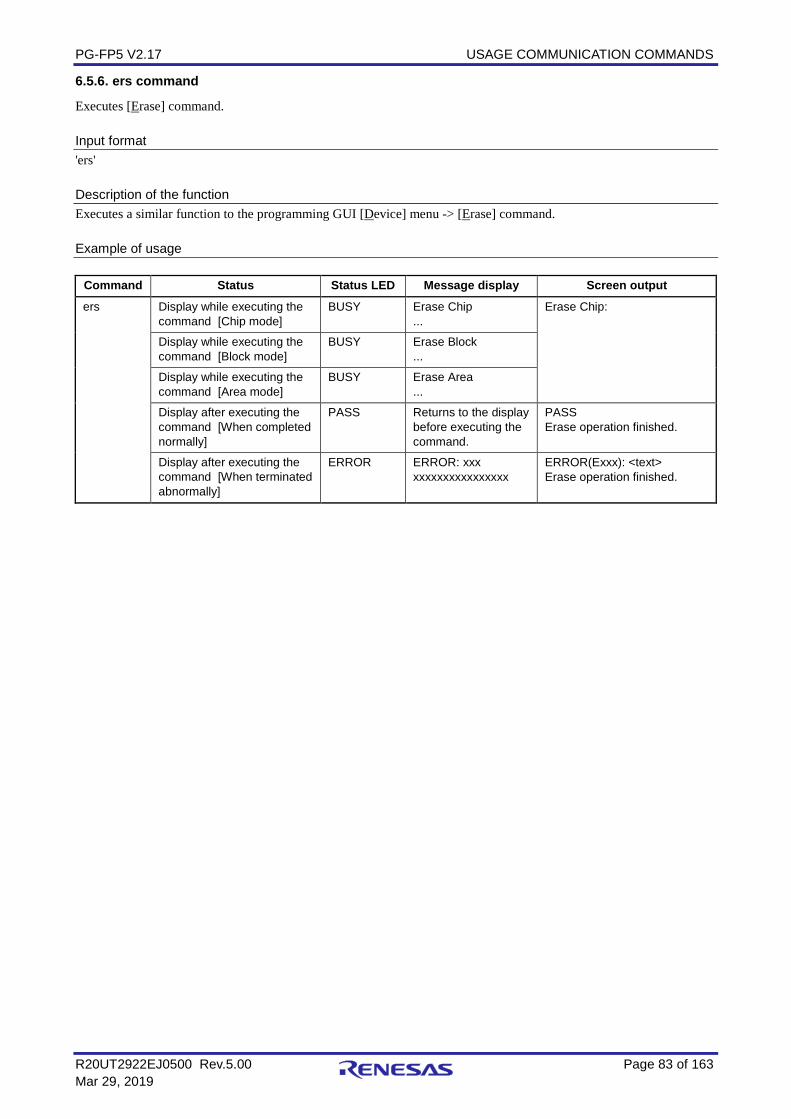
PG-FP5 V2.17 USAGE COMMUNICATION COMMANDS
R20UT2922EJ0500 Rev.5.00 Page 83 of 163 Mar 29, 2019
6.5.6. ers command
Executes [Erase] command. Input format 'ers' Description of the function Executes a similar function to the programming GUI [Device] menu -> [Erase] command. Example of usage
Command Status Status LED Message display Screen output ers Display while executing the
command [Chip mode] BUSY Erase Chip
... Erase Chip:
Display while executing the command [Block mode]
BUSY Erase Block ...
Display while executing the command [Area mode]
BUSY Erase Area ...
Display after executing the command [When completed normally]
PASS Returns to the display before executing the command.
PASS Erase operation finished.
Display after executing the command [When terminated abnormally]
ERROR ERROR: xxx xxxxxxxxxxxxxxxx
ERROR(Exxx): <text> Erase operation finished.
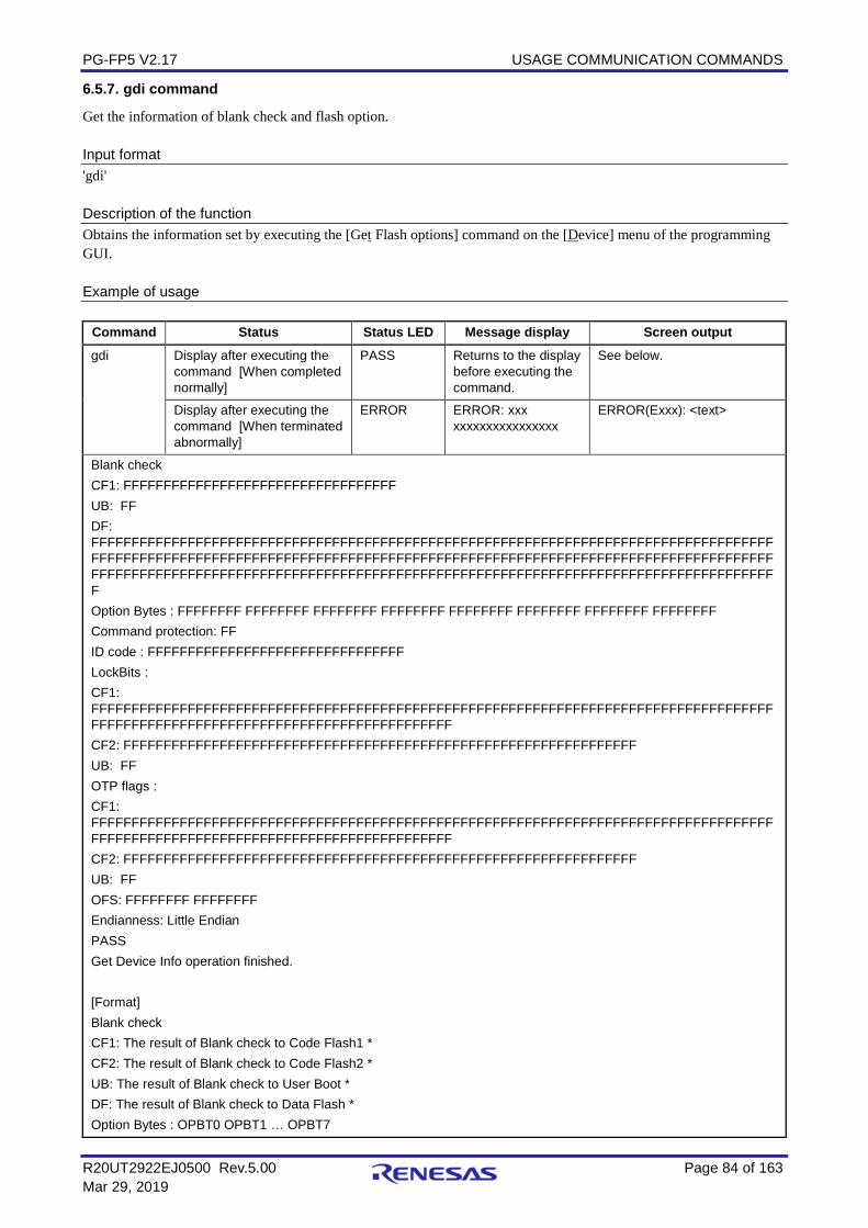
PG-FP5 V2.17 USAGE COMMUNICATION COMMANDS
R20UT2922EJ0500 Rev.5.00 Page 84 of 163 Mar 29, 2019
6.5.7. gdi command
Get the information of blank check and flash option. Input format 'gdi' Description of the function Obtains the information set by executing the [Get Flash options] command on the [Device] menu of the programming GUI. Example of usage
Command Status Status LED Message display Screen output gdi Display after executing the
command [When completed normally]
PASS Returns to the display before executing the command.
See below.
Display after executing the command [When terminated abnormally]
ERROR ERROR: xxx xxxxxxxxxxxxxxxx
ERROR(Exxx): <text>
Blank check CF1: FFFFFFFFFFFFFFFFFFFFFFFFFFFFFFFFFF UB: FF DF: FFFFFFFFFFFFFFFFFFFFFFFFFFFFFFFFFFFFFFFFFFFFFFFFFFFFFFFFFFFFFFFFFFFFFFFFFFFFFFFFFFFFFFFFFFFFFFFFFFFFFFFFFFFFFFFFFFFFFFFFFFFFFFFFFFFFFFFFFFFFFFFFFFFFFFFFFFFFFFFFFFFFFFFFFFFFFFFFFFFFFFFFFFFFFFFFFFFFFFFFFFFFFFFFFFFFFFFFFFFFFFFFFFFFFFFFFFFFFFFFFFFFFFFFFFFFFFFF Option Bytes : FFFFFFFF FFFFFFFF FFFFFFFF FFFFFFFF FFFFFFFF FFFFFFFF FFFFFFFF FFFFFFFF Command protection: FF ID code : FFFFFFFFFFFFFFFFFFFFFFFFFFFFFFFF LockBits : CF1: FFFFFFFFFFFFFFFFFFFFFFFFFFFFFFFFFFFFFFFFFFFFFFFFFFFFFFFFFFFFFFFFFFFFFFFFFFFFFFFFFFFFFFFFFFFFFFFFFFFFFFFFFFFFFFFFFFFFFFFFFFFFFFFFFF CF2: FFFFFFFFFFFFFFFFFFFFFFFFFFFFFFFFFFFFFFFFFFFFFFFFFFFFFFFFFFFFFFFF UB: FF OTP flags : CF1: FFFFFFFFFFFFFFFFFFFFFFFFFFFFFFFFFFFFFFFFFFFFFFFFFFFFFFFFFFFFFFFFFFFFFFFFFFFFFFFFFFFFFFFFFFFFFFFFFFFFFFFFFFFFFFFFFFFFFFFFFFFFFFFFFF CF2: FFFFFFFFFFFFFFFFFFFFFFFFFFFFFFFFFFFFFFFFFFFFFFFFFFFFFFFFFFFFFFFF UB: FF OFS: FFFFFFFF FFFFFFFF Endianness: Little Endian PASS Get Device Info operation finished. [Format] Blank check CF1: The result of Blank check to Code Flash1 * CF2: The result of Blank check to Code Flash2 * UB: The result of Blank check to User Boot * DF: The result of Blank check to Data Flash * Option Bytes : OPBT0 OPBT1 … OPBT7
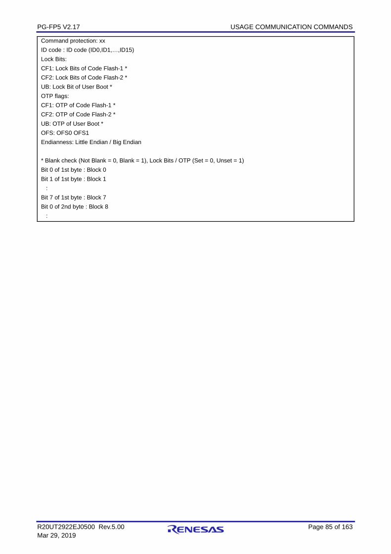
PG-FP5 V2.17 USAGE COMMUNICATION COMMANDS
R20UT2922EJ0500 Rev.5.00 Page 85 of 163 Mar 29, 2019
Command protection: xx ID code : ID code (ID0,ID1,…,ID15) Lock Bits: CF1: Lock Bits of Code Flash-1 * CF2: Lock Bits of Code Flash-2 * UB: Lock Bit of User Boot * OTP flags: CF1: OTP of Code Flash-1 * CF2: OTP of Code Flash-2 * UB: OTP of User Boot * OFS: OFS0 OFS1 Endianness: Little Endian / Big Endian * Blank check (Not Blank = 0, Blank = 1), Lock Bits / OTP (Set = 0, Unset = 1) Bit 0 of 1st byte : Block 0 Bit 1 of 1st byte : Block 1 : Bit 7 of 1st byte : Block 7 Bit 0 of 2nd byte : Block 8 :
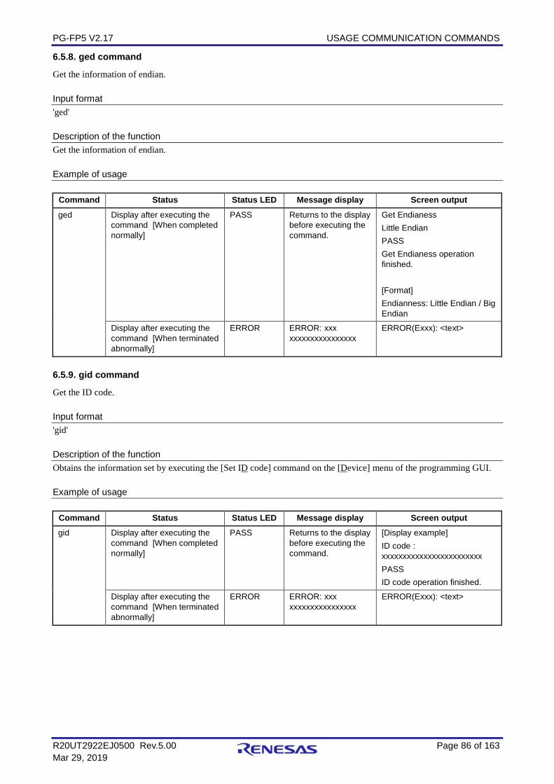
PG-FP5 V2.17 USAGE COMMUNICATION COMMANDS
R20UT2922EJ0500 Rev.5.00 Page 86 of 163 Mar 29, 2019
6.5.8. ged command
Get the information of endian. Input format 'ged' Description of the function Get the information of endian. Example of usage
Command Status Status LED Message display Screen output ged Display after executing the
command [When completed normally]
PASS Returns to the display before executing the command.
Get Endianess Little Endian PASS Get Endianess operation finished. [Format] Endianness: Little Endian / Big Endian
Display after executing the command [When terminated abnormally]
ERROR ERROR: xxx xxxxxxxxxxxxxxxx
ERROR(Exxx): <text>
6.5.9. gid command
Get the ID code. Input format 'gid' Description of the function Obtains the information set by executing the [Set ID code] command on the [Device] menu of the programming GUI. Example of usage
Command Status Status LED Message display Screen output gid Display after executing the
command [When completed normally]
PASS Returns to the display before executing the command.
[Display example] ID code : xxxxxxxxxxxxxxxxxxxxxxxx PASS ID code operation finished.
Display after executing the command [When terminated abnormally]
ERROR ERROR: xxx xxxxxxxxxxxxxxxx
ERROR(Exxx): <text>
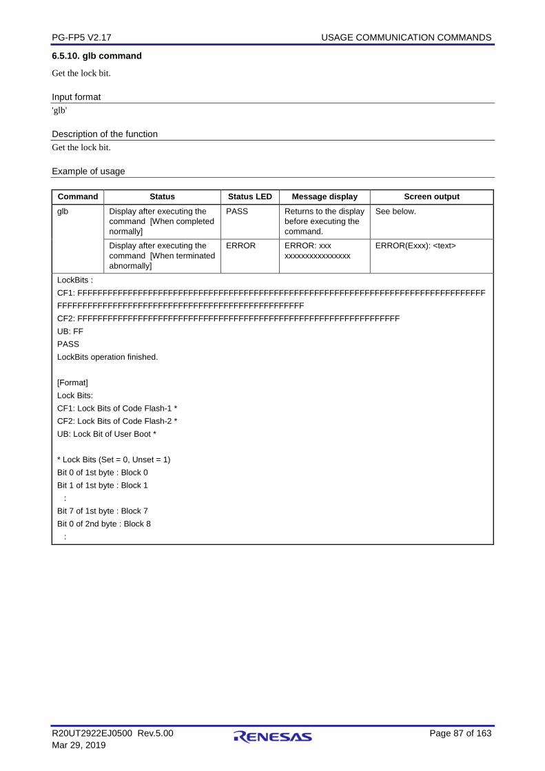
PG-FP5 V2.17 USAGE COMMUNICATION COMMANDS
R20UT2922EJ0500 Rev.5.00 Page 87 of 163 Mar 29, 2019
6.5.10. glb command
Get the lock bit. Input format 'glb' Description of the function Get the lock bit. Example of usage
Command Status Status LED Message display Screen output glb Display after executing the
command [When completed normally]
PASS Returns to the display before executing the command.
See below.
Display after executing the command [When terminated abnormally]
ERROR ERROR: xxx xxxxxxxxxxxxxxxx
ERROR(Exxx): <text>
LockBits : CF1: FFFFFFFFFFFFFFFFFFFFFFFFFFFFFFFFFFFFFFFFFFFFFFFFFFFFFFFFFFFFFFFFFFFFFFFFFFFFFFFFF FFFFFFFFFFFFFFFFFFFFFFFFFFFFFFFFFFFFFFFFFFFFFFFFF CF2: FFFFFFFFFFFFFFFFFFFFFFFFFFFFFFFFFFFFFFFFFFFFFFFFFFFFFFFFFFFFFFFF UB: FF PASS LockBits operation finished. [Format] Lock Bits: CF1: Lock Bits of Code Flash-1 * CF2: Lock Bits of Code Flash-2 * UB: Lock Bit of User Boot * * Lock Bits (Set = 0, Unset = 1) Bit 0 of 1st byte : Block 0 Bit 1 of 1st byte : Block 1 : Bit 7 of 1st byte : Block 7 Bit 0 of 2nd byte : Block 8 :
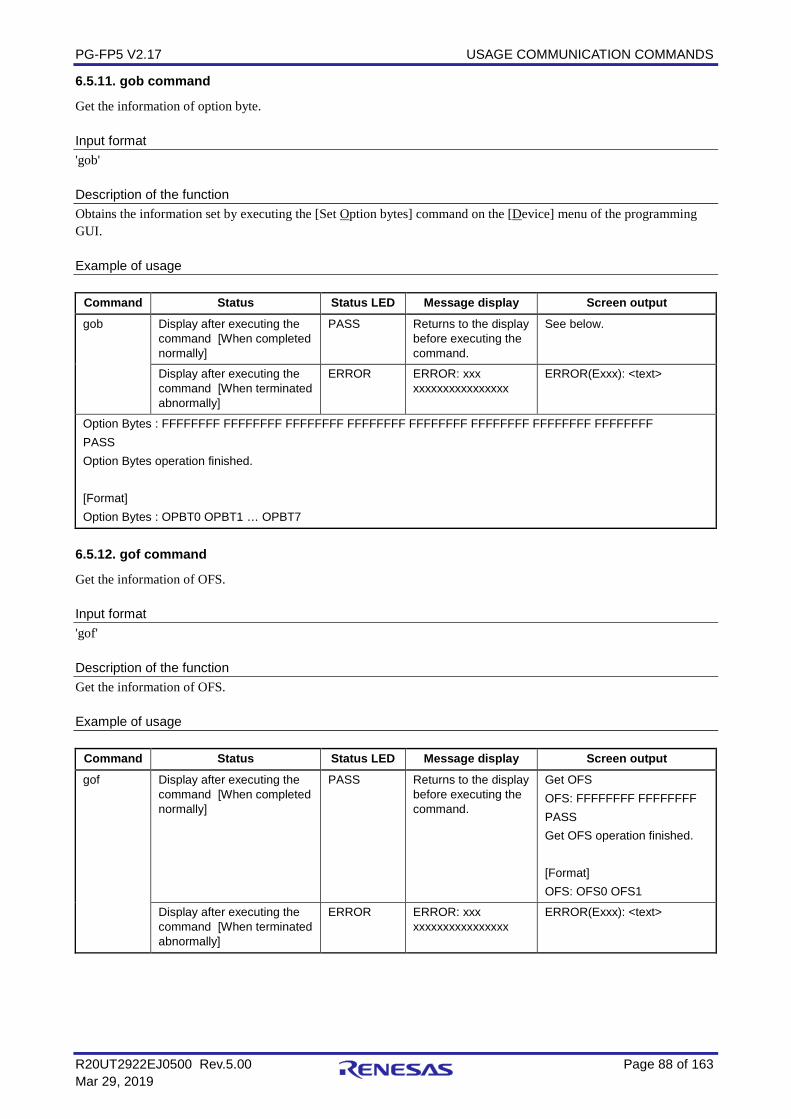
PG-FP5 V2.17 USAGE COMMUNICATION COMMANDS
R20UT2922EJ0500 Rev.5.00 Page 88 of 163 Mar 29, 2019
6.5.11. gob command
Get the information of option byte. Input format 'gob' Description of the function Obtains the information set by executing the [Set Option bytes] command on the [Device] menu of the programming GUI. Example of usage
Command Status Status LED Message display Screen output gob Display after executing the
command [When completed normally]
PASS Returns to the display before executing the command.
See below.
Display after executing the command [When terminated abnormally]
ERROR ERROR: xxx xxxxxxxxxxxxxxxx
ERROR(Exxx): <text>
Option Bytes : FFFFFFFF FFFFFFFF FFFFFFFF FFFFFFFF FFFFFFFF FFFFFFFF FFFFFFFF FFFFFFFF PASS Option Bytes operation finished. [Format] Option Bytes : OPBT0 OPBT1 … OPBT7
6.5.12. gof command
Get the information of OFS. Input format 'gof' Description of the function Get the information of OFS. Example of usage
Command Status Status LED Message display Screen output gof Display after executing the
command [When completed normally]
PASS Returns to the display before executing the command.
Get OFS OFS: FFFFFFFF FFFFFFFF PASS Get OFS operation finished. [Format] OFS: OFS0 OFS1
Display after executing the command [When terminated abnormally]
ERROR ERROR: xxx xxxxxxxxxxxxxxxx
ERROR(Exxx): <text>
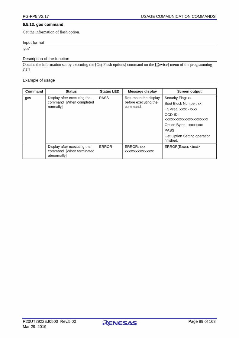
PG-FP5 V2.17 USAGE COMMUNICATION COMMANDS
R20UT2922EJ0500 Rev.5.00 Page 89 of 163 Mar 29, 2019
6.5.13. gos command
Get the information of flash option. Input format 'gos' Description of the function Obtains the information set by executing the [Get Flash options] command on the [Device] menu of the programming GUI. Example of usage
Command Status Status LED Message display Screen output gos Display after executing the
command [When completed normally]
PASS Returns to the display before executing the command.
Security Flag: xx Boot Block Number: xx FS area: xxxx - xxxx OCD-ID : xxxxxxxxxxxxxxxxxxxxxxxx Option Bytes : xxxxxxxx PASS Get Option Setting operation finished.
Display after executing the command [When terminated abnormally]
ERROR ERROR: xxx xxxxxxxxxxxxxxxx
ERROR(Exxx): <text>
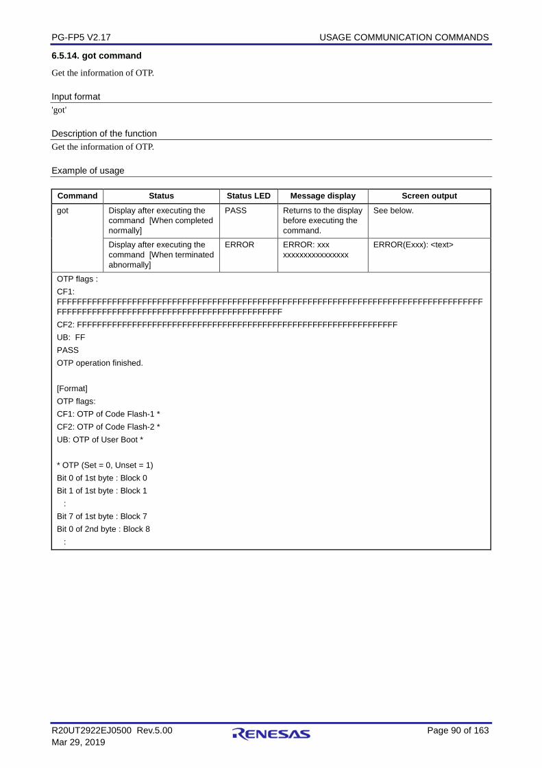
PG-FP5 V2.17 USAGE COMMUNICATION COMMANDS
R20UT2922EJ0500 Rev.5.00 Page 90 of 163 Mar 29, 2019
6.5.14. got command
Get the information of OTP. Input format 'got' Description of the function Get the information of OTP. Example of usage
Command Status Status LED Message display Screen output got Display after executing the
command [When completed normally]
PASS Returns to the display before executing the command.
See below.
Display after executing the command [When terminated abnormally]
ERROR ERROR: xxx xxxxxxxxxxxxxxxx
ERROR(Exxx): <text>
OTP flags : CF1: FFFFFFFFFFFFFFFFFFFFFFFFFFFFFFFFFFFFFFFFFFFFFFFFFFFFFFFFFFFFFFFFFFFFFFFFFFFFFFFFFFFFFFFFFFFFFFFFFFFFFFFFFFFFFFFFFFFFFFFFFFFFFFFFFF CF2: FFFFFFFFFFFFFFFFFFFFFFFFFFFFFFFFFFFFFFFFFFFFFFFFFFFFFFFFFFFFFFFF UB: FF PASS OTP operation finished. [Format] OTP flags: CF1: OTP of Code Flash-1 * CF2: OTP of Code Flash-2 * UB: OTP of User Boot * * OTP (Set = 0, Unset = 1) Bit 0 of 1st byte : Block 0 Bit 1 of 1st byte : Block 1 : Bit 7 of 1st byte : Block 7 Bit 0 of 2nd byte : Block 8 :
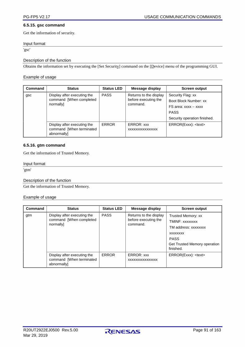
PG-FP5 V2.17 USAGE COMMUNICATION COMMANDS
R20UT2922EJ0500 Rev.5.00 Page 91 of 163 Mar 29, 2019
6.5.15. gsc command
Get the information of security. Input format 'gsc' Description of the function Obtains the information set by executing the [Set Security] command on the [Device] menu of the programming GUI. Example of usage
Command Status Status LED Message display Screen output gsc Display after executing the
command [When completed normally]
PASS Returns to the display before executing the command.
Security Flag: xx Boot Block Number: xx FS area: xxxx – xxxx PASS Security operation finished.
Display after executing the command [When terminated abnormally]
ERROR ERROR: xxx xxxxxxxxxxxxxxxx
ERROR(Exxx): <text>
6.5.16. gtm command
Get the information of Trusted Memory. Input format 'gtm' Description of the function Get the information of Trusted Memory. Example of usage
Command Status Status LED Message display Screen output gtm Display after executing the
command [When completed normally]
PASS Returns to the display before executing the command.
Trusted Memory: xx TMINF: xxxxxxxx TM address: xxxxxxxx xxxxxxxx PASS Get Trusted Memory operation finished.
Display after executing the command [When terminated abnormally]
ERROR ERROR: xxx xxxxxxxxxxxxxxxx
ERROR(Exxx): <text>
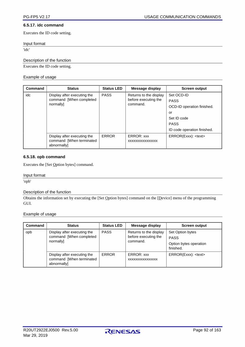
PG-FP5 V2.17 USAGE COMMUNICATION COMMANDS
R20UT2922EJ0500 Rev.5.00 Page 92 of 163 Mar 29, 2019
6.5.17. idc command
Executes the ID code setting. Input format 'idc' Description of the function Executes the ID code setting. Example of usage
Command Status Status LED Message display Screen output idc Display after executing the
command [When completed normally]
PASS Returns to the display before executing the command.
Set OCD-ID PASS OCD-ID operation finished. or Set ID code PASS ID code operation finished.
Display after executing the command [When terminated abnormally]
ERROR ERROR: xxx xxxxxxxxxxxxxxxx
ERROR(Exxx): <text>
6.5.18. opb command
Executes the [Set Option bytes] command. Input format 'opb' Description of the function Obtains the information set by executing the [Set Option bytes] command on the [Device] menu of the programming GUI. Example of usage
Command Status Status LED Message display Screen output opb Display after executing the
command [When completed normally]
PASS Returns to the display before executing the command.
Set Option bytes PASS Option bytes operation finished.
Display after executing the command [When terminated abnormally]
ERROR ERROR: xxx xxxxxxxxxxxxxxxx
ERROR(Exxx): <text>
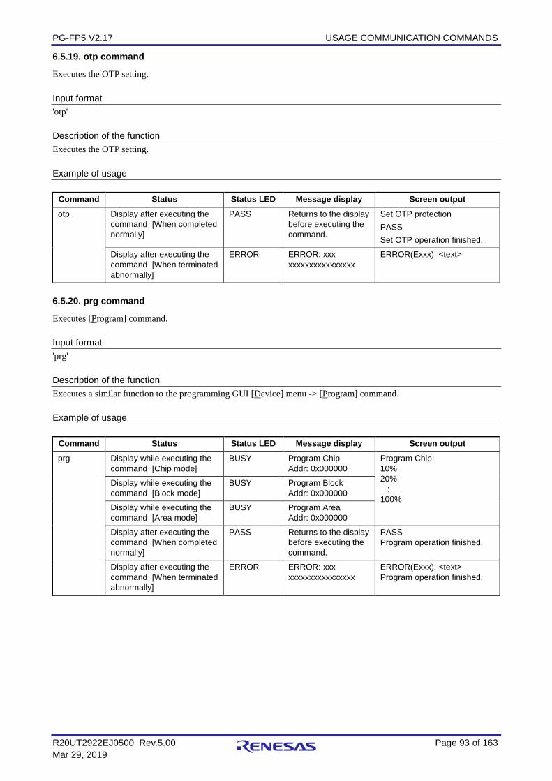
PG-FP5 V2.17 USAGE COMMUNICATION COMMANDS
R20UT2922EJ0500 Rev.5.00 Page 93 of 163 Mar 29, 2019
6.5.19. otp command
Executes the OTP setting. Input format 'otp' Description of the function Executes the OTP setting. Example of usage
Command Status Status LED Message display Screen output otp Display after executing the
command [When completed normally]
PASS Returns to the display before executing the command.
Set OTP protection PASS Set OTP operation finished.
Display after executing the command [When terminated abnormally]
ERROR ERROR: xxx xxxxxxxxxxxxxxxx
ERROR(Exxx): <text>
6.5.20. prg command
Executes [Program] command. Input format 'prg' Description of the function Executes a similar function to the programming GUI [Device] menu -> [Program] command. Example of usage
Command Status Status LED Message display Screen output prg Display while executing the
command [Chip mode] BUSY Program Chip
Addr: 0x000000 Program Chip: 10% 20% : 100%
Display while executing the command [Block mode]
BUSY Program Block Addr: 0x000000
Display while executing the command [Area mode]
BUSY Program Area Addr: 0x000000
Display after executing the command [When completed normally]
PASS Returns to the display before executing the command.
PASS Program operation finished.
Display after executing the command [When terminated abnormally]
ERROR ERROR: xxx xxxxxxxxxxxxxxxx
ERROR(Exxx): <text> Program operation finished.
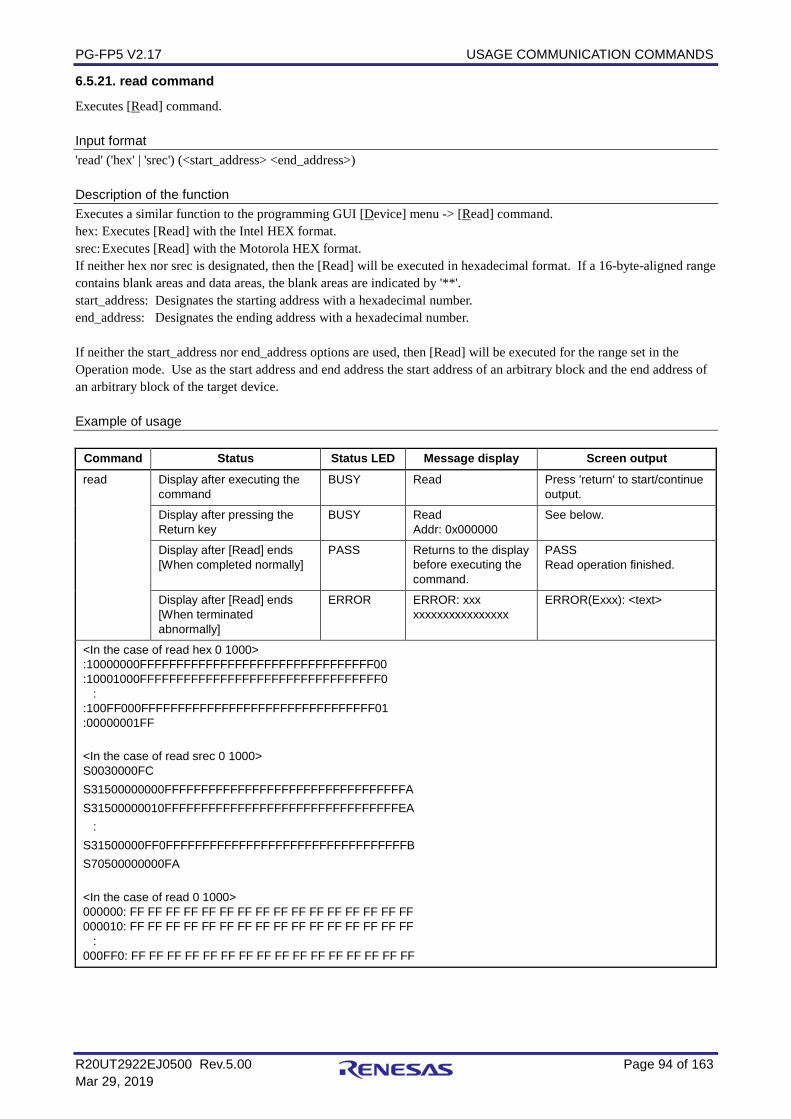
PG-FP5 V2.17 USAGE COMMUNICATION COMMANDS
R20UT2922EJ0500 Rev.5.00 Page 94 of 163 Mar 29, 2019
6.5.21. read command
Executes [Read] command. Input format 'read' ('hex' | 'srec') (<start_address> <end_address>) Description of the function Executes a similar function to the programming GUI [Device] menu -> [Read] command. hex: Executes [Read] with the Intel HEX format. srec: Executes [Read] with the Motorola HEX format. If neither hex nor srec is designated, then the [Read] will be executed in hexadecimal format. If a 16-byte-aligned range contains blank areas and data areas, the blank areas are indicated by '**'. start_address: Designates the starting address with a hexadecimal number. end_address: Designates the ending address with a hexadecimal number. If neither the start_address nor end_address options are used, then [Read] will be executed for the range set in the Operation mode. Use as the start address and end address the start address of an arbitrary block and the end address of an arbitrary block of the target device. Example of usage
Command Status Status LED Message display Screen output read Display after executing the
command BUSY Read Press 'return' to start/continue
output.
Display after pressing the Return key
BUSY Read Addr: 0x000000
See below.
Display after [Read] ends [When completed normally]
PASS Returns to the display before executing the command.
PASS Read operation finished.
Display after [Read] ends [When terminated abnormally]
ERROR ERROR: xxx xxxxxxxxxxxxxxxx
ERROR(Exxx): <text>
<In the case of read hex 0 1000> :10000000FFFFFFFFFFFFFFFFFFFFFFFFFFFFFFFF00 :10001000FFFFFFFFFFFFFFFFFFFFFFFFFFFFFFFFF0 : :100FF000FFFFFFFFFFFFFFFFFFFFFFFFFFFFFFFF01 :00000001FF <In the case of read srec 0 1000> S0030000FC S31500000000FFFFFFFFFFFFFFFFFFFFFFFFFFFFFFFFFA S31500000010FFFFFFFFFFFFFFFFFFFFFFFFFFFFFFFFEA : S31500000FF0FFFFFFFFFFFFFFFFFFFFFFFFFFFFFFFFFB S70500000000FA <In the case of read 0 1000> 000000: FF FF FF FF FF FF FF FF FF FF FF FF FF FF FF FF 000010: FF FF FF FF FF FF FF FF FF FF FF FF FF FF FF FF : 000FF0: FF FF FF FF FF FF FF FF FF FF FF FF FF FF FF FF
PG-FP5 V2.17 USAGE COMMUNICATION COMMANDS
R20UT2922EJ0500 Rev.5.00 Page 95 of 163 Mar 29, 2019
6.5.22. rsc command
Executes the Security Release command. Input format 'rsc' Description of the function Executes the Security Release command. Example of usage
Command Status Status LED Message display Screen output rsc Display after executing the
command [When completed normally]
PASS Returns to the display before executing the command.
Release security PASS Release security operation finished.
Display after executing the command [When terminated abnormally]
ERROR ERROR: xxx xxxxxxxxxxxxxxxx
ERROR(Exxx): <text>
6.5.23. scf command
Executes [Set Security] command. Input format 'scf' Description of the function Executes a similar function to the programming GUI [Device] menu -> [Set Security] command. Example of usage
Command Status Status LED Message display Screen output scf Display after executing the
command [When completed normally]
PASS Returns to the display before executing the command.
Set Security Flags PASS Security operation finished. or Set command protection PASS Set comm. prot. operation finished.
Display after executing the command [When terminated abnormally]
ERROR ERROR: xxx xxxxxxxxxxxxxxxx
ERROR(Exxx): <text>
PG-FP5 V2.17 USAGE COMMUNICATION COMMANDS
R20UT2922EJ0500 Rev.5.00 Page 96 of 163 Mar 29, 2019
6.5.24. sed command
Executes the endian setting. Input format 'sed' Description of the function Executes the endian setting. Example of usage
Command Status Status LED Message display Screen output sed Display after executing the
command [When completed normally]
PASS Returns to the display before executing the command.
Set Endianness PASS Set Endianness operation finished.
Display after executing the command [When terminated abnormally]
ERROR ERROR: xxx xxxxxxxxxxxxxxxx
ERROR(Exxx): <text>
6.5.25. sid command
Sets the ID code and enables ID authentication in the serial programming mode. Input format 'sid' (<ID Code>) ID Code : Specifies the ID code to be set. When the sid command is specified, the specified ID code is set for the target device instead of the ID code stored in the ESF file. Description of the function Sets the ID code and enables ID authentication in the serial programming mode. Example of usage
Command Status Status LED Message display Screen output sid Display after executing the
command [When completed normally]
PASS Returns to the display before executing the command.
Set Serial Programming ID PASS Serial Progr. ID operation finished.
Display after executing the command [When terminated abnormally]
ERROR ERROR: xxx xxxxxxxxxxxxxxxx
ERROR(Exxx): <text>
PG-FP5 V2.17 USAGE COMMUNICATION COMMANDS
R20UT2922EJ0500 Rev.5.00 Page 97 of 163 Mar 29, 2019
6.5.26. sig command
Executes [Signature read] command. Input format 'sig' Description of the function Executes a similar function to the programming GUI [Device] menu -> [Signature read] command. Example of usage
Command Status Status LED Message display Screen output sig Display while executing the
command BUSY Signature: Device name: Dxxxxxxxxx
Device data: xx xx xx xx Device end addr: xxxxxxxx Security Flag: xxxx Boot Block Number: xxxx Device Version: x.xx Firmware Version: x.xx
Display after executing the command [When completed normally]
PASS Returns to the display before executing the command.
PASS Signature operation finished.
Display after executing the command [When terminated abnormally]
ERROR ERROR: xxx xxxxxxxxxxxxxxxx
ERROR(Exxx): <text>
6.5.27. slb command
Executes the Lock bits setting. Input format 'slb' Description of the function Executes the Lock bits setting. Example of usage
Command Status Status LED Message display Screen output slb Display after executing the
command [When completed normally]
PASS Returns to the display before executing the command.
Set LockBits PASS LockBits operation finished.
Display after executing the command [When terminated abnormally]
ERROR ERROR: xxx xxxxxxxxxxxxxxxx
ERROR(Exxx): <text>
PG-FP5 V2.17 USAGE COMMUNICATION COMMANDS
R20UT2922EJ0500 Rev.5.00 Page 98 of 163 Mar 29, 2019
6.5.28. spd command
Executes the disable serial programming setting. Input format 'spd' Description of the function Executes the disable serial programming setting. Example of usage
Command Status Status LED Message display Screen output spd Display after executing the
command [When completed normally]
PASS Returns to the display before executing the command.
Set Serial Programming Disable PASS Set SerProgDis operation finished.
Display after executing the command [When terminated abnormally]
ERROR ERROR: xxx xxxxxxxxxxxxxxxx
ERROR(Exxx): <text>
6.5.29. stm command
Executes the Trusted Memory setting. Input format 'stm' Description of the function Executes the Trusted Memory setting. Example of usage
Command Status Status LED Message display Screen output stm Display after executing the
command [When completed normally]
PASS Returns to the display before executing the command.
Set Trusted Memory PASS Set Trusted Memory operation finished.
Display after executing the command [When terminated abnormally]
ERROR ERROR: xxx xxxxxxxxxxxxxxxx
ERROR(Exxx): <text>
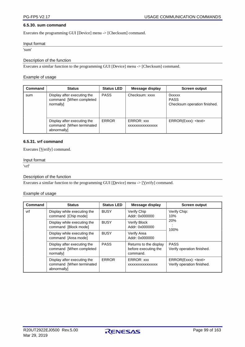
PG-FP5 V2.17 USAGE COMMUNICATION COMMANDS
R20UT2922EJ0500 Rev.5.00 Page 99 of 163 Mar 29, 2019
6.5.30. sum command
Executes the programming GUI [Device] menu -> [Checksum] command. Input format 'sum' Description of the function Executes a similar function to the programming GUI [Device] menu -> [Checksum] command. Example of usage
Command Status Status LED Message display Screen output sum Display after executing the
command [When completed normally]
PASS Checksum: xxxx 0xxxxx PASS Checksum operation finished.
Display after executing the command [When terminated abnormally]
ERROR ERROR: xxx xxxxxxxxxxxxxxxx
ERROR(Exxx): <text>
6.5.31. vrf command
Executes [Verify] command. Input format 'vrf' Description of the function Executes a similar function to the programming GUI [Device] menu -> [Verify] command. Example of usage
Command Status Status LED Message display Screen output vrf Display while executing the
command [Chip mode] BUSY Verify Chip
Addr: 0x000000 Verify Chip: 10% 20% : 100%
Display while executing the command [Block mode]
BUSY Verify Block Addr: 0x000000
Display while executing the command [Area mode]
BUSY Verify Area Addr: 0x000000
Display after executing the command [When completed normally]
PASS Returns to the display before executing the command.
PASS Verify operation finished.
Display after executing the command [When terminated abnormally]
ERROR ERROR: xxx xxxxxxxxxxxxxxxx
ERROR(Exxx): <text> Verify operation finished.
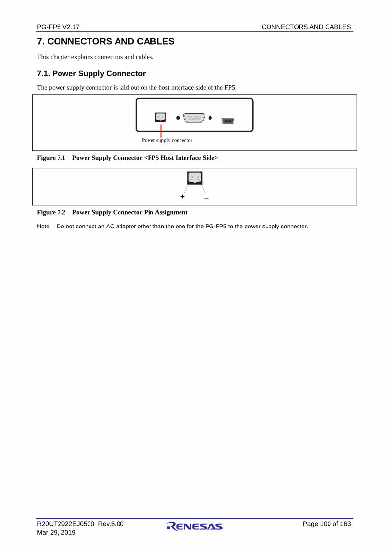
PG-FP5 V2.17 CONNECTORS AND CABLES
R20UT2922EJ0500 Rev.5.00 Page 100 of 163 Mar 29, 2019
7. CONNECTORS AND CABLES This chapter explains connectors and cables. 7.1. Power Supply Connector The power supply connector is laid out on the host interface side of the FP5.
Figure 7.1 Power Supply Connector <FP5 Host Interface Side>
+ −
Figure 7.2 Power Supply Connector Pin Assignment
Note Do not connect an AC adaptor other than the one for the PG-FP5 to the power supply connecter.
Power supply connector
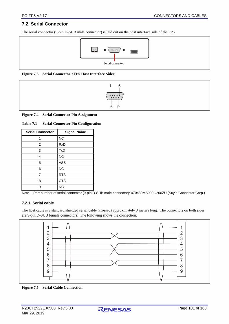
PG-FP5 V2.17 CONNECTORS AND CABLES
R20UT2922EJ0500 Rev.5.00 Page 101 of 163 Mar 29, 2019
7.2. Serial Connector The serial connector (9-pin D-SUB male connector) is laid out on the host interface side of the FP5.
Figure 7.3 Serial Connector <FP5 Host Interface Side>
1 5
9 6
Figure 7.4 Serial Connector Pin Assignment
Table 7.1 Serial Connector Pin Configuration
Serial Connector Signal Name
1 NC
2 RxD
3 TxD
4 NC
5 VSS
6 NC
7 RTS
8 CTS
9 NC
Note Part number of serial connector (9-pin D-SUB male connector): 070430MB009G200ZU (Suyin Connector Corp.) 7.2.1. Serial cable
The host cable is a standard shielded serial cable (crossed) approximately 3 meters long. The connectors on both sides are 9-pin D-SUB female connectors. The following shows the connection.
Figure 7.5 Serial Cable Connection
Serial connector
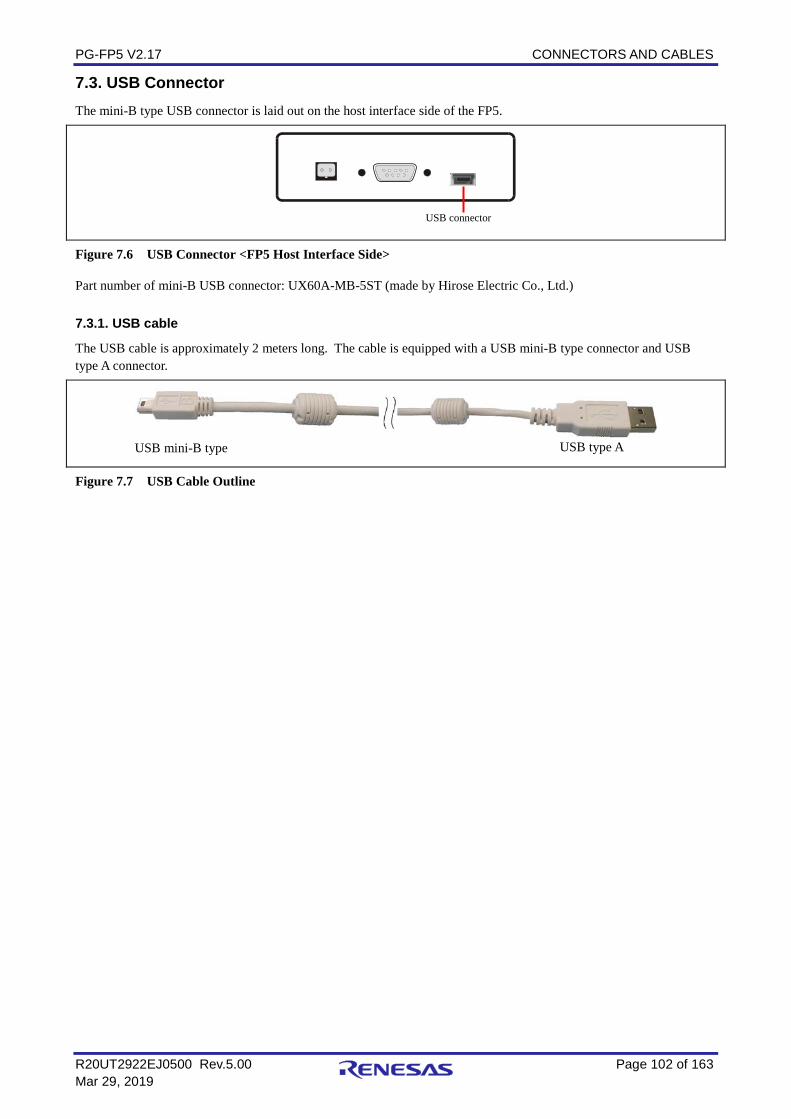
PG-FP5 V2.17 CONNECTORS AND CABLES
R20UT2922EJ0500 Rev.5.00 Page 102 of 163 Mar 29, 2019
7.3. USB Connector The mini-B type USB connector is laid out on the host interface side of the FP5.
Figure 7.6 USB Connector <FP5 Host Interface Side>
Part number of mini-B USB connector: UX60A-MB-5ST (made by Hirose Electric Co., Ltd.)
7.3.1. USB cable
The USB cable is approximately 2 meters long. The cable is equipped with a USB mini-B type connector and USB type A connector.
Figure 7.7 USB Cable Outline
USB connector
USB mini-B type USB type A
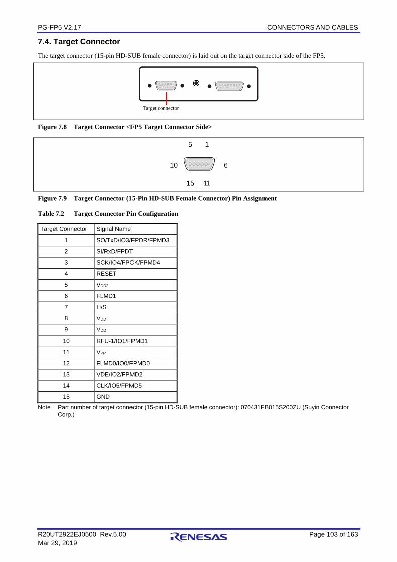
PG-FP5 V2.17 CONNECTORS AND CABLES
R20UT2922EJ0500 Rev.5.00 Page 103 of 163 Mar 29, 2019
7.4. Target Connector The target connector (15-pin HD-SUB female connector) is laid out on the target connector side of the FP5.
Figure 7.8 Target Connector <FP5 Target Connector Side>
1 5
10
11
6
15
Figure 7.9 Target Connector (15-Pin HD-SUB Female Connector) Pin Assignment
Table 7.2 Target Connector Pin Configuration
Target Connector Signal Name
1 SO/TxD/IO3/FPDR/FPMD3
2 SI/RxD/FPDT
3 SCK/IO4/FPCK/FPMD4
4 RESET¯¯¯¯¯¯
5 VDD2
6 FLMD1
7 H/S
8 VDD
9 VDD
10 RFU-1/IO1/FPMD1
11 VPP
12 FLMD0/IO0/FPMD0
13 VDE/IO2/FPMD2
14 CLK/IO5/FPMD5
15 GND
Note Part number of target connector (15-pin HD-SUB female connector): 070431FB015S200ZU (Suyin Connector Corp.)
Target connector
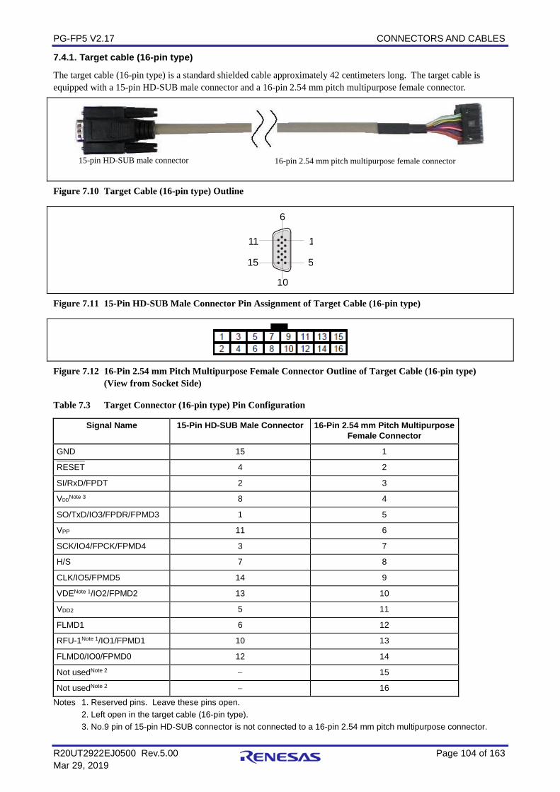
PG-FP5 V2.17 CONNECTORS AND CABLES
R20UT2922EJ0500 Rev.5.00 Page 104 of 163 Mar 29, 2019
7.4.1. Target cable (16-pin type)
The target cable (16-pin type) is a standard shielded cable approximately 42 centimeters long. The target cable is equipped with a 15-pin HD-SUB male connector and a 16-pin 2.54 mm pitch multipurpose female connector.
Figure 7.10 Target Cable (16-pin type) Outline
1
5
6
11
10
15
Figure 7.11 15-Pin HD-SUB Male Connector Pin Assignment of Target Cable (16-pin type)
Figure 7.12 16-Pin 2.54 mm Pitch Multipurpose Female Connector Outline of Target Cable (16-pin type) (View from Socket Side)
Table 7.3 Target Connector (16-pin type) Pin Configuration
Signal Name 15-Pin HD-SUB Male Connector 16-Pin 2.54 mm Pitch Multipurpose Female Connector
GND 15 1
RESET¯¯¯¯¯¯ 4 2
SI/RxD/FPDT 2 3
VDDNote 3 8 4
SO/TxD/IO3/FPDR/FPMD3 1 5
VPP 11 6
SCK/IO4/FPCK/FPMD4 3 7
H/S 7 8
CLK/IO5/FPMD5 14 9
VDENote 1/IO2/FPMD2 13 10
VDD2 5 11
FLMD1 6 12
RFU-1Note 1/IO1/FPMD1 10 13
FLMD0/IO0/FPMD0 12 14
Not usedNote 2 − 15
Not usedNote 2 − 16 Notes 1. Reserved pins. Leave these pins open. 2. Left open in the target cable (16-pin type). 3. No.9 pin of 15-pin HD-SUB connector is not connected to a 16-pin 2.54 mm pitch multipurpose connector.
16-pin 2.54 mm pitch multipurpose female connector 15-pin HD-SUB male connector
PG-FP5 V2.17 CONNECTORS AND CABLES
R20UT2922EJ0500 Rev.5.00 Page 105 of 163 Mar 29, 2019
Note The following are the recommended connectors to be connected to 16-pin 2.54 mm pitch multipurpose female connectors.
• HIF3FC-16PA-2.54DS (made by Hirose Electric Co., Ltd., right angle type) • HIF3FC-16PA-2.54DSA (made by Hirose Electric Co., Ltd., straight type) • 7616-5002PL (Sumitomo 3M Limited, right angle type) • 7616-6002PL (Sumitomo 3M Limited, straight type) When using a self-made cable because the supplied cable cannot be used due to the target system specifications, the cable characteristics should be equivalent or higher than those of the supplied cable. Note that communication may be performed at high speed depending on the communication settings. Consequently, communication errors may occur and causing abnormal operation.
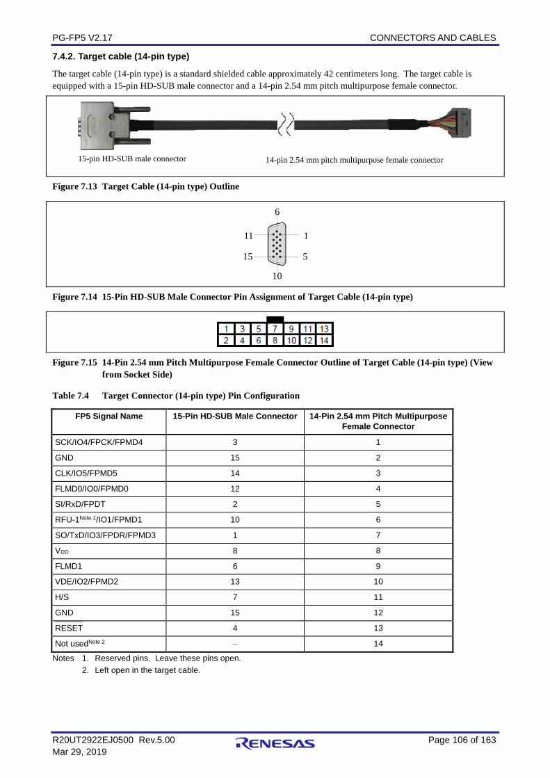
PG-FP5 V2.17 CONNECTORS AND CABLES
R20UT2922EJ0500 Rev.5.00 Page 106 of 163 Mar 29, 2019
7.4.2. Target cable (14-pin type)
The target cable (14-pin type) is a standard shielded cable approximately 42 centimeters long. The target cable is equipped with a 15-pin HD-SUB male connector and a 14-pin 2.54 mm pitch multipurpose female connector.
Figure 7.13 Target Cable (14-pin type) Outline
1
5
6
11
10
15
Figure 7.14 15-Pin HD-SUB Male Connector Pin Assignment of Target Cable (14-pin type)
Figure 7.15 14-Pin 2.54 mm Pitch Multipurpose Female Connector Outline of Target Cable (14-pin type) (View from Socket Side)
Table 7.4 Target Connector (14-pin type) Pin Configuration
FP5 Signal Name 15-Pin HD-SUB Male Connector 14-Pin 2.54 mm Pitch Multipurpose Female Connector
SCK/IO4/FPCK/FPMD4 3 1
GND 15 2
CLK/IO5/FPMD5 14 3
FLMD0/IO0/FPMD0 12 4
SI/RxD/FPDT 2 5
RFU-1Note 1/IO1/FPMD1 10 6
SO/TxD/IO3/FPDR/FPMD3 1 7
VDD 8 8
FLMD1 6 9
VDE/IO2/FPMD2 13 10
H/S 7 11
GND 15 12
RESET¯¯¯¯¯¯ 4 13
Not usedNote 2 − 14
Notes 1. Reserved pins. Leave these pins open. 2. Left open in the target cable.
14-pin 2.54 mm pitch multipurpose female connector 15-pin HD-SUB male connector
PG-FP5 V2.17 CONNECTORS AND CABLES
R20UT2922EJ0500 Rev.5.00 Page 107 of 163 Mar 29, 2019
Note The following are the recommended connectors to be connected to 14-pin 2.54 mm pitch multipurpose female connectors.
• 7614-6002 (Sumitomo 3M Limited, straight type) • 2514-6002 (3M Limited, straight type) When using a self-made cable because the target cable cannot be used due to the target system specifications, the cable characteristics should be equivalent or higher than those of the target cable. Note that communication may be performed at high speed depending on the communication settings. Consequently, communication errors may occur and causing abnormal operation.
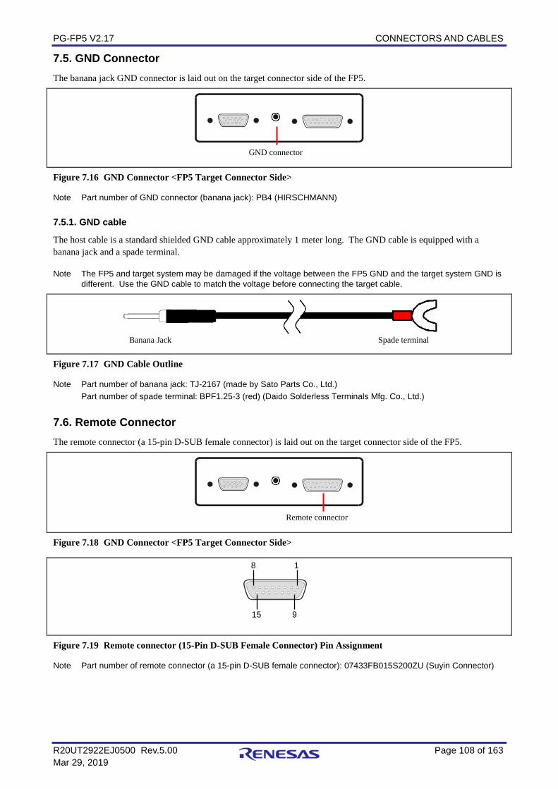
PG-FP5 V2.17 CONNECTORS AND CABLES
R20UT2922EJ0500 Rev.5.00 Page 108 of 163 Mar 29, 2019
7.5. GND Connector The banana jack GND connector is laid out on the target connector side of the FP5.
Figure 7.16 GND Connector <FP5 Target Connector Side>
Note Part number of GND connector (banana jack): PB4 (HIRSCHMANN) 7.5.1. GND cable
The host cable is a standard shielded GND cable approximately 1 meter long. The GND cable is equipped with a banana jack and a spade terminal. Note The FP5 and target system may be damaged if the voltage between the FP5 GND and the target system GND is
different. Use the GND cable to match the voltage before connecting the target cable.
Figure 7.17 GND Cable Outline
Note Part number of banana jack: TJ-2167 (made by Sato Parts Co., Ltd.) Part number of spade terminal: BPF1.25-3 (red) (Daido Solderless Terminals Mfg. Co., Ltd.) 7.6. Remote Connector The remote connector (a 15-pin D-SUB female connector) is laid out on the target connector side of the FP5.
Figure 7.18 GND Connector <FP5 Target Connector Side>
Figure 7.19 Remote connector (15-Pin D-SUB Female Connector) Pin Assignment
Note Part number of remote connector (a 15-pin D-SUB female connector): 07433FB015S200ZU (Suyin Connector)
GND connector
Banana Jack Spade terminal
Remote connector
15 9
8 1
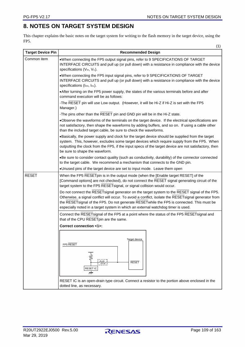
PG-FP5 V2.17 NOTES ON TARGET SYSTEM DESIGN
R20UT2922EJ0500 Rev.5.00 Page 109 of 163 Mar 29, 2019
8. NOTES ON TARGET SYSTEM DESIGN This chapter explains the basic notes on the target system for writing to the flash memory in the target device, using the FP5.
(1) Target Device Pin Recommended Design Common item •When connecting the FP5 output signal pins, refer to 9 SPECIFICATIONS OF TARGET
INTERFACE CIRCUITS and pull up (or pull down) with a resistance in compliance with the device specifications (VIH, VIL). •When connecting the FP5 input signal pins, refer to 9 SPECIFICATIONS OF TARGET INTERFACE CIRCUITS and pull up (or pull down) with a resistance in compliance with the device specifications (IOH, IOL). •After turning on the FP5 power supply, the states of the various terminals before and after command execution will be as follows:
-The RESET¯¯¯¯¯¯ pin will use Low output. (However, it will be Hi-Z if Hi-Z is set with the FP5 Manager.)
-The pins other than the RESET¯¯¯¯¯¯ pin and GND pin will be in the Hi-Z state. •Observe the waveforms of the terminals on the target device. If the electrical specifications are not satisfactory, then shape the waveforms by adding buffers, and so on. If using a cable other than the included target cable, be sure to check the waveforms. •Basically, the power supply and clock for the target device should be supplied from the target system. This, however, excludes some target devices which require supply from the FP5. When outputting the clock from the FP5, if the input specs of the target device are not satisfactory, then be sure to shape the waveform. •Be sure to consider contact quality (such as conductivity, durability) of the connector connected to the target cable. We recommend a mechanism that connects to the GND pin. •Unused pins of the target device are set to input mode. Leave them open
RESET¯¯¯¯¯¯ When the FP5 RESET¯¯¯¯¯¯pin is in the output mode (when the [Enable target RESET] of the [Command options] are not checked), do not connect the RESET¯¯¯¯¯¯ signal generating circuit of the target system to the FP5 RESET¯¯¯¯¯¯signal, or signal collision would occur.
Do not connect the RESET¯¯¯¯¯¯signal generator on the target system to the RESET¯¯¯¯¯¯ signal of the FP5. Otherwise, a signal conflict will occur. To avoid a conflict, isolate the RESET¯¯¯¯¯¯signal generator from the RESET¯¯¯¯¯¯signal of the FP5. Do not generate RESET¯¯¯¯¯¯while the FP5 is connected. This must be especially noted in a target system in which an external watchdog timer is used.
Connect the RESET¯¯¯¯¯¯signal of the FP5 at a point where the status of the FP5 RESET¯¯¯¯¯¯signal and that of the CPU RESET¯¯¯¯¯¯pin are the same.
Correct connection <1>:
Target device
FP5 RESET
RESET RESET IC
RESET IC is an open-drain type circuit. Connect a resistor to the portion above enclosed in the dotted line, as necessary.
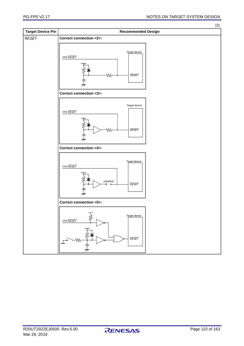
PG-FP5 V2.17 NOTES ON TARGET SYSTEM DESIGN
R20UT2922EJ0500 Rev.5.00 Page 110 of 163 Mar 29, 2019
(2) Target Device Pin Recommended Design
RESET¯¯¯¯¯¯ Correct connection <2>:
Target device
FP5 RESET
RESET
Correct connection <3>:
Target device FP5 RESET
RESET
Correct connection <4>:
Target device
FP5 RESET
RESET JUMPER
Correct connection <5>:
Target device
FP5 RESET
RESET
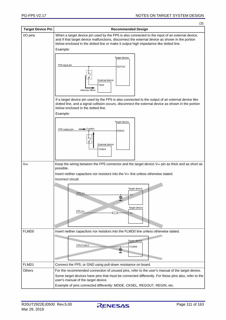
PG-FP5 V2.17 NOTES ON TARGET SYSTEM DESIGN
R20UT2922EJ0500 Rev.5.00 Page 111 of 163 Mar 29, 2019
(3) Target Device Pin Recommended Design I/O pins When a target device pin used by the FP5 is also connected to the input of an external device,
and if that target device malfunctions, disconnect the external device as shown in the portion below enclosed in the dotted line or make it output high impedance like dotted line.
Example:
Adverse effect
FP5 input pin
Input External device
SO/TxD
Target device
If a target device pin used by the FP5 is also connected to the output of an external device like
dotted line, and a signal collision occurs, disconnect the external device as shown in the portion below enclosed in the dotted line.
Example:
Conflict FP5 output pin
Output External device
SI/RxD
Target device
VPP Keep the wiring between the FP5 connector and the target device VPP pin as thick and as short as
possible. Insert neither capacitors nor resistors into the VPP line unless otherwise stated.
Incorrect circuit:
VPP
FP5 VPP
FP5 VPP
VPP
Target device
Target device
FLMD0 Insert neither capacitors nor resistors into the FLMD0 line unless otherwise stated. Target device
FLMD0 FP5 FLML0
FLMD1 Connect the FP5, or GND using pull-down resistance on board.
Others For the recommended connection of unused pins, refer to the user’s manual of the target device. Some target devices have pins that must be connected differently. For these pins also, refer to the user’s manual of the target device. Example of pins connected differently: MODE, CKSEL, REGOUT, REGIN, etc.
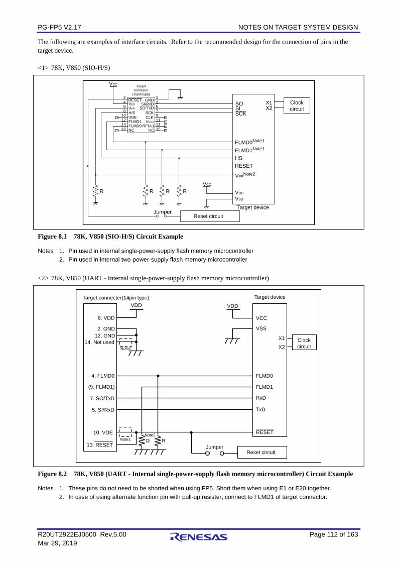
PG-FP5 V2.17 NOTES ON TARGET SYSTEM DESIGN
R20UT2922EJ0500 Rev.5.00 Page 112 of 163 Mar 29, 2019
The following are examples of interface circuits. Refer to the recommended design for the connection of pins in the target device. <1> 78K, V850 (SIO-H/S)
FLMD1Note1
JumperReset circuit
VCC
Target device
FLMD0Note1
VDD
VSS
R R
SOSI
R
VPPNote2
R
HS
2468
10121416
RESETVDDVPPH/SVDEFLMD1FLMD0NC
SO/TxDSCKCLKVDD2
RFU-1NC
13579111315
Targetconnecter
(16pin type)
X1X2
Clockcircuit
VCC
GNDSI/RxD
RESET
SCK
Figure 8.1 78K, V850 (SIO-H/S) Circuit Example
Notes 1. Pin used in internal single-power-supply flash memory microcontroller 2. Pin used in internal two-power-supply flash memory microcontroller <2> 78K, V850 (UART - Internal single-power-supply flash memory microcontroller)
VSS
VCC
RESET
8. VDD
VDD VDD
RxD7. SO/TxD
FLMD0
FLMD1
4. FLMD0
(9. FLMD1)
TxD5. SI/RxD
X1X2
2. GND12. GND
14. Not used
R R
Target deviceTarget connecter(14pin type)
Reset circuitJumper
Clockcircuit
Note2
Note1
13. RESET
10. VDENote1
Figure 8.2 78K, V850 (UART - Internal single-power-supply flash memory microcontroller) Circuit Example
Notes 1. These pins do not need to be shorted when using FP5. Short them when using E1 or E20 together. 2. In case of using alternate function pin with pull-up resister, connect to FLMD1 of target connector.
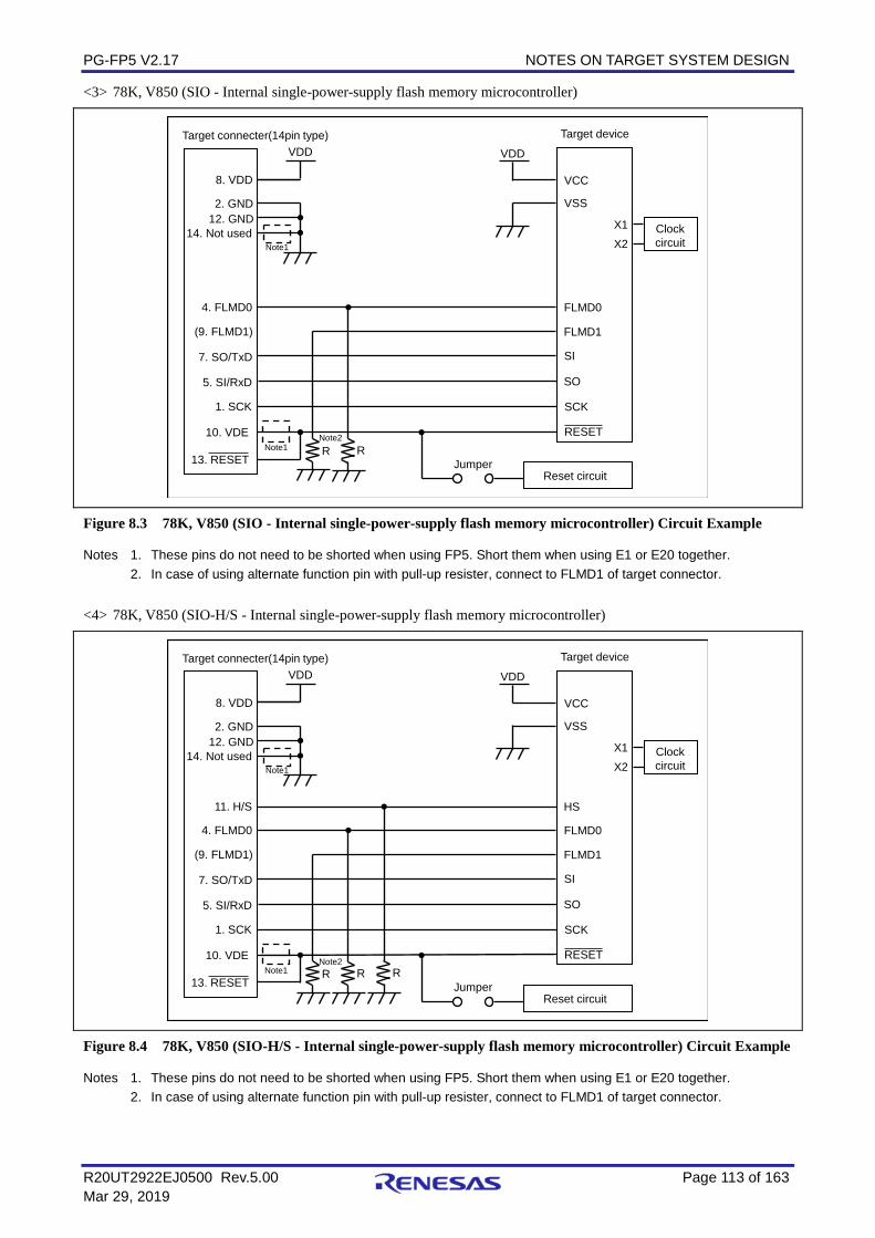
PG-FP5 V2.17 NOTES ON TARGET SYSTEM DESIGN
R20UT2922EJ0500 Rev.5.00 Page 113 of 163 Mar 29, 2019
<3> 78K, V850 (SIO - Internal single-power-supply flash memory microcontroller)
VSS
VCC
RESET
8. VDD
VDD VDD
SI7. SO/TxD
FLMD0
FLMD1
4. FLMD0
(9. FLMD1)
SO5. SI/RxD
1. SCK SCK
X1X2
2. GND12. GND
14. Not used
R R
Target deviceTarget connecter(14pin type)
Reset circuitJumper
Clockcircuit
Note2
Note1
13. RESET
10. VDENote1
Figure 8.3 78K, V850 (SIO - Internal single-power-supply flash memory microcontroller) Circuit Example
Notes 1. These pins do not need to be shorted when using FP5. Short them when using E1 or E20 together. 2. In case of using alternate function pin with pull-up resister, connect to FLMD1 of target connector. <4> 78K, V850 (SIO-H/S - Internal single-power-supply flash memory microcontroller)
VSS
VCC
RESET
8. VDD
VDD VDD
SI7. SO/TxD
FLMD0
FLMD1
4. FLMD0
(9. FLMD1)
SO5. SI/RxD
1. SCK SCK
X1X2
2. GND12. GND
14. Not used
R R
HS11. H/S
R
Target deviceTarget connecter(14pin type)
Reset circuitJumper
Clockcircuit
Note2
Note1
13. RESET
10. VDENote1
Figure 8.4 78K, V850 (SIO-H/S - Internal single-power-supply flash memory microcontroller) Circuit Example
Notes 1. These pins do not need to be shorted when using FP5. Short them when using E1 or E20 together. 2. In case of using alternate function pin with pull-up resister, connect to FLMD1 of target connector.
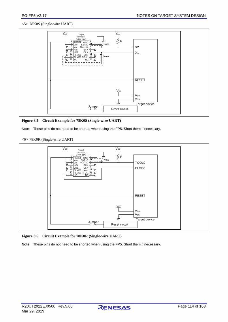
PG-FP5 V2.17 NOTES ON TARGET SYSTEM DESIGN
R20UT2922EJ0500 Rev.5.00 Page 114 of 163 Mar 29, 2019
<5> 78K0S (Single-wire UART)
VCC
Note
VDD
VSS
RESET
X1
X2
2468
10121416
RESETVDDVPPH/SVDEFLMD1FLMD0NC
GNDSI/RxD
SO/TxDSCKCLKVDD2
RFU-1NC
13579111315
VCC
Note
VCC
R
JumperReset circuit
Target device
Targetconnecter
(16pin type)
Figure 8.5 Circuit Example for 78K0S (Single-wire UART)
Note These pins do not need to be shorted when using the FP5. Short them if necessary. <6> 78K0R (Single-wire UART)
VCC
VDD
VSS
RESET
FLMD0
TOOL0
2468
10121416
RESETVDDVPPH/SVDEFLMD1FLMD0NC
GNDSI/RxD
SO/TxDSCKCLKVDD2
RFU-1NC
13579111315
VCC
Note
VCC
R
JumperReset circuit
Target device
Targetconnecter
(16pin type)
Figure 8.6 Circuit Example for 78K0R (Single-wire UART)
Note These pins do not need to be shorted when using the FP5. Short them if necessary.
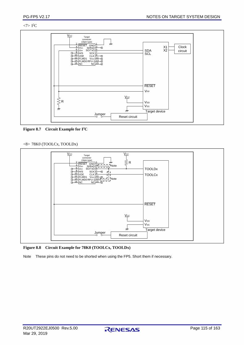
PG-FP5 V2.17 NOTES ON TARGET SYSTEM DESIGN
R20UT2922EJ0500 Rev.5.00 Page 115 of 163 Mar 29, 2019
<7> I2C
VCC
VDD
VSS
RESET
SDASCL
R
VPP
2468
10121416
RESETVDDVPPH/SVDEFLMD1FLMD0NC
GNDSI/RxD
SO/TxDSCKCLKVDD2
RFU-1NC
13579111315
X1X2
VCC
JumperReset circuit
Target device
Targetconnecter
(16pin type)
Clockcircuit
Figure 8.7 Circuit Example for I2C
<8> 78K0 (TOOLCx, TOOLDx)
VCC
Note
VDD
VSS
RESET
TOOLCx
TOOLDx
2468
10121416
RESETVDDVPPH/SVDEFLMD1FLMD0NC
GNDSI/RxD
SO/TxDSCKCLKVDD2
RFU-1NC
13579111315
VCC
Note
VCC
R
JumperReset circuit
Target device
Targetconnecter
(16pin type)
Figure 8.8 Circuit Example for 78K0 (TOOLCx, TOOLDx)
Note These pins do not need to be shorted when using the FP5. Short them if necessary.
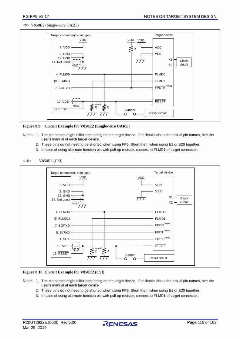
PG-FP5 V2.17 NOTES ON TARGET SYSTEM DESIGN
R20UT2922EJ0500 Rev.5.00 Page 116 of 163 Mar 29, 2019
<9> V850E2 (Single-wire UART)
VSS
VCC
RESET
8. VDD
VDD VDD
FPDTR7. SO/TxD
VDD
R
FLMD0
FLMD1
4. FLMD0
Target deviceTarget connecter(14pin type)
Reset circuitJumper
X1X2
Clockcircuit
Note1
Note3
2. GND
Note2
12. GND14. Not used
R R
(9. FLMD1)
13. RESET
10. VDENote2
Figure 8.9 Circuit Example for V850E2 (Single-wire UART)
Notes 1. The pin names might differ depending on the target device. For details about the actual pin names, see the user’s manual of each target device.
2. These pins do not need to be shorted when using FP5. Short them when using E1 or E20 together. 3. In case of using alternate function pin with pull-up resister, connect to FLMD1 of target connector. <10> V850E2 (CSI)
VSS
VCC
RESET
8. VDD
VDD VDD
FPDR7. SO/TxD
FLMD0
FLMD1
4. FLMD0
FPDT5. SI/RxD
1. SCK FPCK
Target deviceTarget connecter(14pin type)
Reset circuitJumper
X1X2
Clockcircuit
Note1
Note1
Note1
2. GND
Note2
12. GND14. Not used
R RNote3
(9. FLMD1)
13. RESET
10. VDENote2
Figure 8.10 Circuit Example for V850E2 (CSI)
Notes 1. The pin names might differ depending on the target device. For details about the actual pin names, see the user’s manual of each target device.
2. These pins do not need to be shorted when using FP5. Short them when using E1 or E20 together. 3. In case of using alternate function pin with pull-up resister, connect to FLMD1 of target connector.
PG-FP5 V2.17 NOTES ON TARGET SYSTEM DESIGN
R20UT2922EJ0500 Rev.5.00 Page 117 of 163 Mar 29, 2019
<11> RL78 family (VDD = EVDD)
Target deviceTarget connecter(14pin type)
Reset circuitJumper
VSS
TOOL0
VDD
RESET
5. SI/RxD
13. RESET
VDD
10. VDE
EVDD
EVSS
1kΩ
VDD
8. VDD
VDD
2. GND
9. FLMD1
Note
Note
12. GND14. Not used
Note
Figure 8.11 Circuit Example for RL78 Family (VDD = EVDD)
Note These pins do not need to be shorted when using FP5. Short them when using E1 or E20 together. <12> RL78 family (VDD ≠ EVDD)
Target deviceExchange adapter Target connecter(14pin type)
Reset circuitJumper
VSS
TOOL0
VDD
RESET
8. VDD
5. SI/RxD
13. RESET
VDD VDD
1kΩ
10. VDE
EVDD
EVDDEVSS
EVDDEVDD
9. FLMD1
FL-RL78/FP5Note1
Note2
2. GND12. GND
14. Not usedNote2
Figure 8.12 Circuit Example for RL78 Family (VDD ≠ EVDD)
Notes 1. To perform write when VDD ≠ EVDD, connect the conversion adaptor FL-RL78/FP5 (a product of Naito Densei Machida Mfg. Co., Ltd.). On the [Advanced] tab in the Device Setup dialog box, enter the voltage value of VDD in the [Vdd[V]] box, enter 0V in the [Vdd2[V]] box, and select the [On Target] check box. For the system configuration and specifications of the FL-RL78/FP5, refer to the FL-RL78/FP5 User's Manual.
2. These pins do not need to be shorted when using FP5. Short them when using E1 or E20 together.
PG-FP5 V2.17 NOTES ON TARGET SYSTEM DESIGN
R20UT2922EJ0500 Rev.5.00 Page 118 of 163 Mar 29, 2019
<13> RX family, SuperH family (SCI)
10. IO2
7. IO3
Note2
Note2
Note1
Note1
Target deviceTarget connecter(14pin type)
Reset circuitJumper
VSS
TxD
VCC
RESET
2. GND
8. VDD
5. SI/RxD
13. RESET
RxD11. H/S
MD0
MD1
R R R R R
Clockcircuit
VCC VCCVCCVCCVCCVCCVCC
Note3
Note4 Note4 Note4 Note4 Note4
12. GND14. Not used
Note5
Note5
EXTALXTAL
Note6
Note7
Figure 8.13 Circuit Example for RX Family and SuperH Family (SCI) (Circuit Example for RX62T)
Notes 1. For the serial communication interface (SCI) that can be used for writing, refer to the user's manual of the target device.
2. Connect the Mode Setting Pin of Operating Mode to any of the IO0 to IO5 pins. The signal settings for IO0 to IO5 pins can be set in the [I/O Signal Settings] area on the [Advanced] tab in the Device Setup dialog box. For RX62T, set MD0 to High, MD1 to Low, and unused I/O signals to High-Z. Normally, use the initial settings in the [I/O Signal Settings] area. It is compatible with write circuit examples with E1/E20 Emulator Additional Document for User's Manual (RX User System Design).
3. These pins do not need to be shorted when using FP5. Short them when using E1, E20 or E8a together. 4. Set the R value to between 4.7 and 10 kΩ when using E1, E20 or E8a together. 5. The mode setting pins for setting the operating mode may differ with the target device. Refer to the user’s
manual for the target device you are using. 6. The need for the clock circuit might differ depending on the target device. Refer to the user’s manual for the
target device you are using. 7. These pins do not need to pull up when using FP5. Pull up them when using E1, E20 or E8a together.
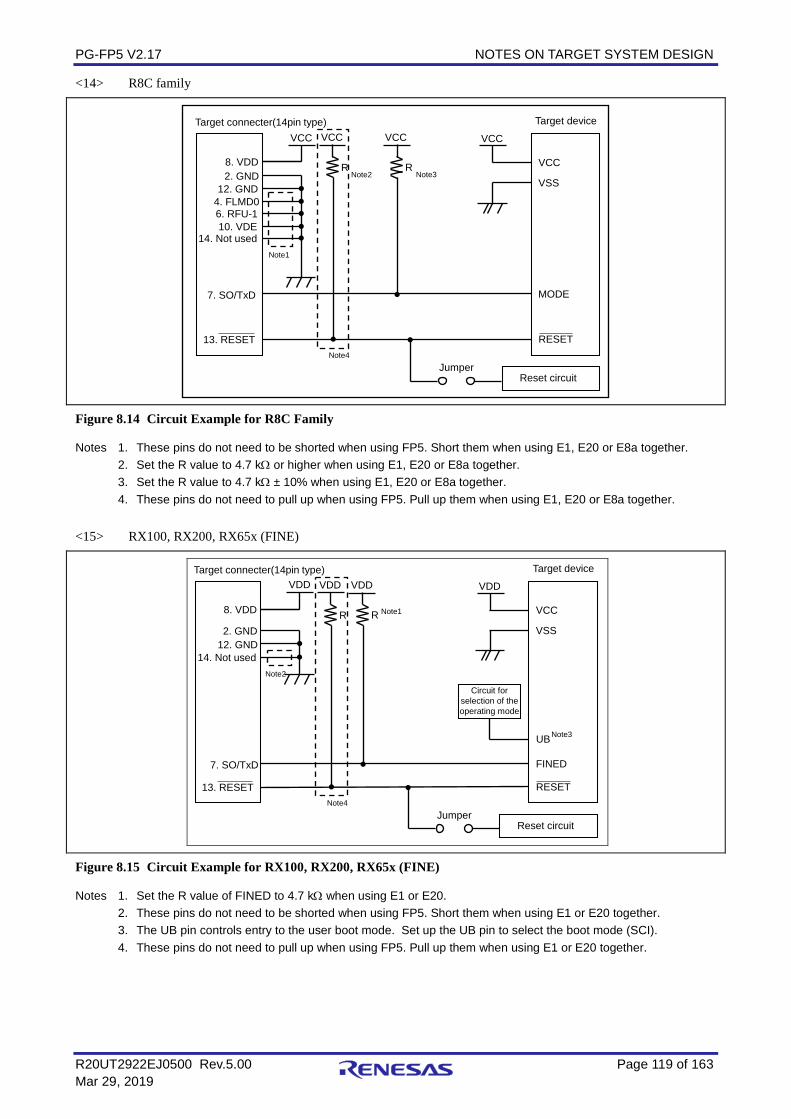
PG-FP5 V2.17 NOTES ON TARGET SYSTEM DESIGN
R20UT2922EJ0500 Rev.5.00 Page 119 of 163 Mar 29, 2019
<14> R8C family
VSS
VCC
RESET
8. VDD
13. RESET
MODE7. SO/TxD
R R
Target deviceTarget connecter(14pin type)
Reset circuitJumper
2. GND12. GND
4. FLMD06. RFU-110. VDE
14. Not usedNote1
VCC VCCVCCVCC
Note2 Note3
Note4
Figure 8.14 Circuit Example for R8C Family
Notes 1. These pins do not need to be shorted when using FP5. Short them when using E1, E20 or E8a together. 2. Set the R value to 4.7 kΩ or higher when using E1, E20 or E8a together. 3. Set the R value to 4.7 kΩ ± 10% when using E1, E20 or E8a together. 4. These pins do not need to pull up when using FP5. Pull up them when using E1, E20 or E8a together. <15> RX100, RX200, RX65x (FINE)
Target deviceTarget connecter(14pin type)
Reset circuitJumper
VSS
FINED
VCC
RESET
8. VDD
7. SO/TxD
13. RESET
VDD VDDVDDVDD
R R
UB
Circuit for selection of the operating mode
2. GND
Note2
12. GND14. Not used
Note1
Note3
Note4
Figure 8.15 Circuit Example for RX100, RX200, RX65x (FINE)
Notes 1. Set the R value of FINED to 4.7 kΩ when using E1 or E20. 2. These pins do not need to be shorted when using FP5. Short them when using E1 or E20 together. 3. The UB pin controls entry to the user boot mode. Set up the UB pin to select the boot mode (SCI). 4. These pins do not need to pull up when using FP5. Pull up them when using E1 or E20 together.
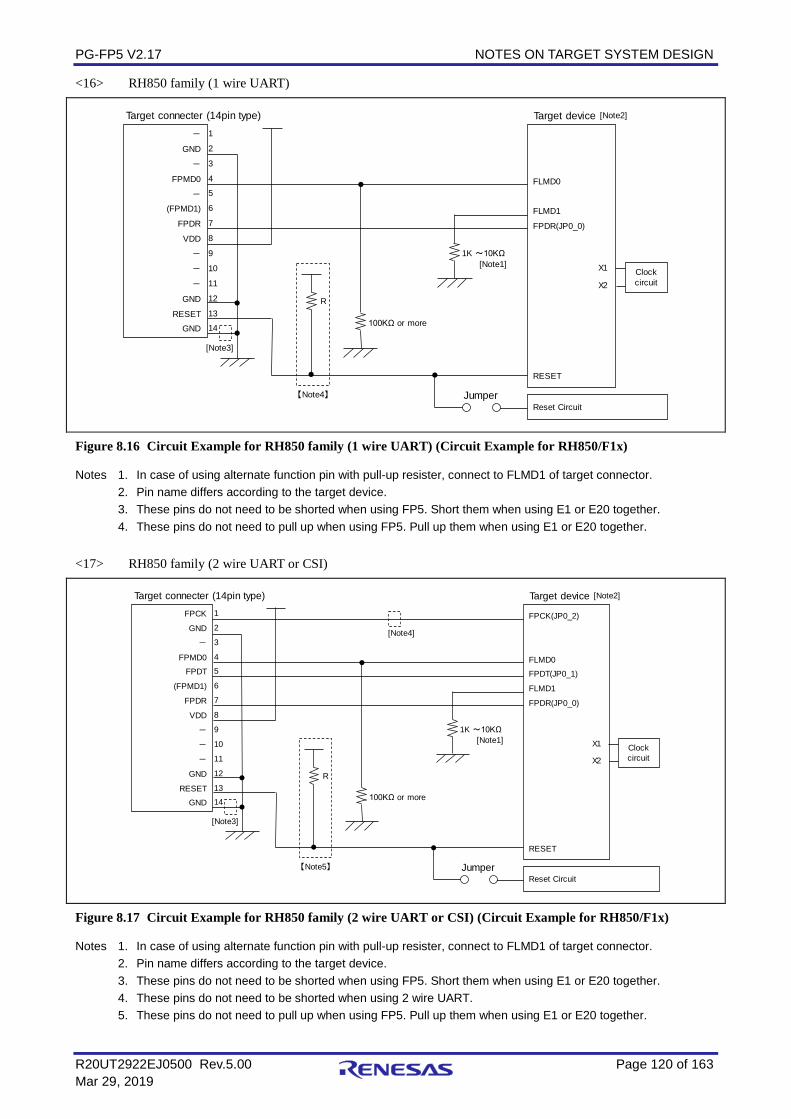
PG-FP5 V2.17 NOTES ON TARGET SYSTEM DESIGN
R20UT2922EJ0500 Rev.5.00 Page 120 of 163 Mar 29, 2019
<16> RH850 family (1 wire UART)
-
GND
-
FPMD0
-
(FPMD1)
FPDR
VDD
-
-
-
GND
RESETGND
1
2
3
45
6
7
8
9
10
11
12
1314
FLMD0
FLMD1
FPDR(JP0_0)
RESET
Reset Circuit
1K ~10KΩ
100KΩ or more
Target device [Note2]
[Note1]
Target connecter (14pin type)
[Note3]
Jumper
X1
X2Clockcircuit
R
【Note4】
Figure 8.16 Circuit Example for RH850 family (1 wire UART) (Circuit Example for RH850/F1x)
Notes 1. In case of using alternate function pin with pull-up resister, connect to FLMD1 of target connector. 2. Pin name differs according to the target device. 3. These pins do not need to be shorted when using FP5. Short them when using E1 or E20 together. 4. These pins do not need to pull up when using FP5. Pull up them when using E1 or E20 together. <17> RH850 family (2 wire UART or CSI)
FPCK
GND
-
FPMD0FPDT
(FPMD1)
FPDR
VDD
-
-
-
GND
RESETGND
1
2
3
45
6
7
8
9
10
11
12
1314
FPCK(JP0_2)
FLMD0FPDT(JP0_1)
FLMD1
FPDR(JP0_0)
RESET
100KΩ or more
1K ~10KΩ[Note1]
Target connecter (14pin type)
[Note3]
Reset CircuitJumper
X1
X2Clockcircuit
Target device [Note2]
[Note4]
R
【Note5】
Figure 8.17 Circuit Example for RH850 family (2 wire UART or CSI) (Circuit Example for RH850/F1x)
Notes 1. In case of using alternate function pin with pull-up resister, connect to FLMD1 of target connector. 2. Pin name differs according to the target device. 3. These pins do not need to be shorted when using FP5. Short them when using E1 or E20 together. 4. These pins do not need to be shorted when using 2 wire UART. 5. These pins do not need to pull up when using FP5. Pull up them when using E1 or E20 together.
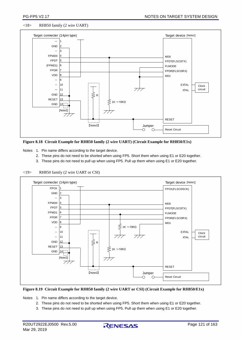
PG-FP5 V2.17 NOTES ON TARGET SYSTEM DESIGN
R20UT2922EJ0500 Rev.5.00 Page 121 of 163 Mar 29, 2019
<18> RH850 family (2 wire UART)
-
GND
-
FPMD0FPDT
(FPMD1)
FPDR
VDD
-
-
-
GND
RESETGND
1
2
3
45
6
7
8
9
10
11
12
1314
MD0FPDT(FLSCI3TX)
FLMODE
FPDR(FLSCI3RX)
MD1
RESET
Target connecter (14pin type)
[Note2]
Reset CircuitJumper
1K ~10KΩ
Clockcircuit
Target device [Note1]
EXTAL
XTAL
R
【Note3】
Figure 8.18 Circuit Example for RH850 family (2 wire UART) (Circuit Example for RH850/E1x)
Notes 1. Pin name differs according to the target device. 2. These pins do not need to be shorted when using FP5. Short them when using E1 or E20 together. 3. These pins do not need to pull up when using FP5. Pull up them when using E1 or E20 together. <19> RH850 family (2 wire UART or CSI)
FPCK
GND
-
FPMD0FPDT
FPMD1
FPDR
VDD
-
-
-
GND
RESETGND
1
2
3
45
6
7
8
9
10
11
12
1314
FPCK(FLSCI3SCK)
MD0FPDT(FLSCI3TX)
FLMODE
FPDR(FLSCI3RX)
MD1
RESET
Target connecter (14pin type)
[Note2]
Reset CircuitJumper
1K ~10KΩ
1K ~10KΩ
Clockcircuit
Target device [Note1]
EXTAL
XTAL
R
【Note3】
Figure 8.19 Circuit Example for RH850 family (2 wire UART or CSI) (Circuit Example for RH850/E1x)
Notes 1. Pin name differs according to the target device. 2. These pins do not need to be shorted when using FP5. Short them when using E1 or E20 together. 3. These pins do not need to pull up when using FP5. Pull up them when using E1 or E20 together.
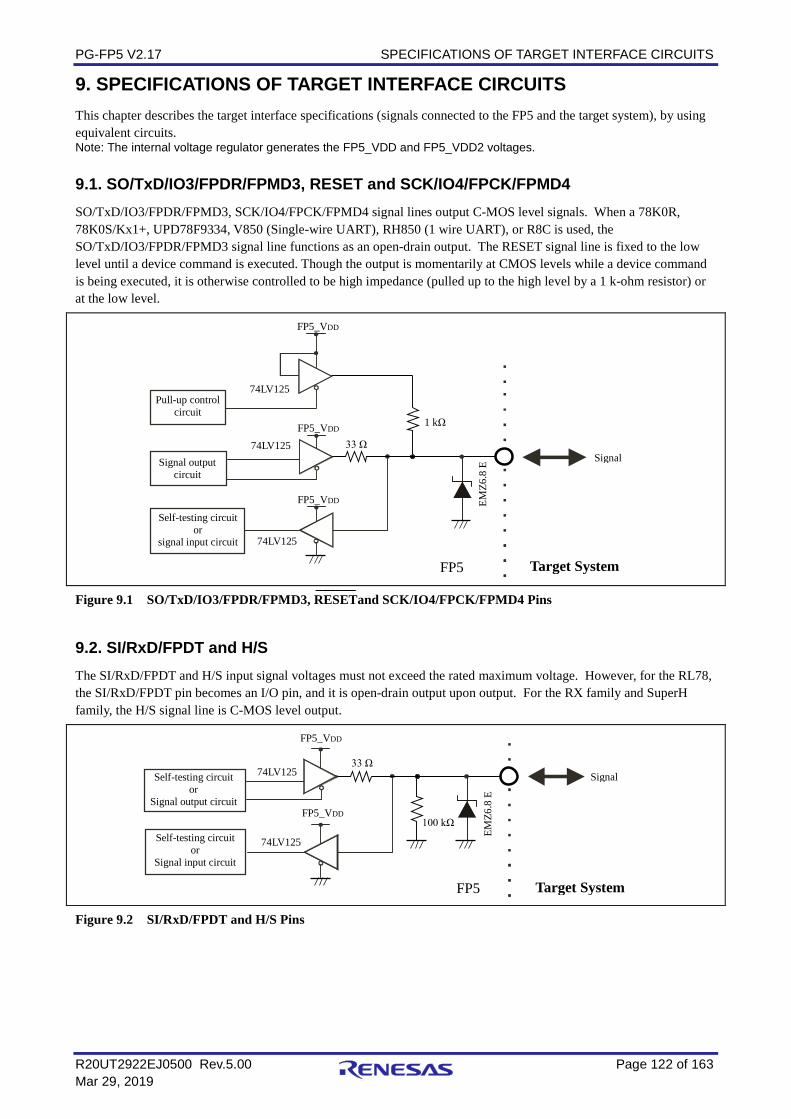
PG-FP5 V2.17 SPECIFICATIONS OF TARGET INTERFACE CIRCUITS
R20UT2922EJ0500 Rev.5.00 Page 122 of 163 Mar 29, 2019
9. SPECIFICATIONS OF TARGET INTERFACE CIRCUITS This chapter describes the target interface specifications (signals connected to the FP5 and the target system), by using equivalent circuits. Note: The internal voltage regulator generates the FP5_VDD and FP5_VDD2 voltages. 9.1. SO/TxD/IO3/FPDR/FPMD3, RESET and SCK/IO4/FPCK/FPMD4 SO/TxD/IO3/FPDR/FPMD3, SCK/IO4/FPCK/FPMD4 signal lines output C-MOS level signals. When a 78K0R, 78K0S/Kx1+, UPD78F9334, V850 (Single-wire UART), RH850 (1 wire UART), or R8C is used, the SO/TxD/IO3/FPDR/FPMD3 signal line functions as an open-drain output. The RESET signal line is fixed to the low level until a device command is executed. Though the output is momentarily at CMOS levels while a device command is being executed, it is otherwise controlled to be high impedance (pulled up to the high level by a 1 k-ohm resistor) or at the low level.
Figure 9.1 SO/TxD/IO3/FPDR/FPMD3, RESET¯¯¯¯¯¯ and SCK/IO4/FPCK/FPMD4 Pins
9.2. SI/RxD/FPDT and H/S The SI/RxD/FPDT and H/S input signal voltages must not exceed the rated maximum voltage. However, for the RL78, the SI/RxD/FPDT pin becomes an I/O pin, and it is open-drain output upon output. For the RX family and SuperH family, the H/S signal line is C-MOS level output.
Figure 9.2 SI/RxD/FPDT and H/S Pins
FP5
33 Ω
EMZ6
.8 E
Self-testing circuit or
Signal output circuit
Self-testing circuit or
Signal input circuit
74LV125
74LV125
FP5_VDD
Signal
Target System
100 kΩ
FP5_VDD
1 kΩ
FP5
74LV125
74LV125
Signal 33 Ω
Target System
EMZ6
.8 E
74LV125
FP5_VDD
FP5_VDD
FP5_VDD
Pull-up control circuit
Signal output circuit
Self-testing circuit or
signal input circuit
PG-FP5 V2.17 SPECIFICATIONS OF TARGET INTERFACE CIRCUITS
R20UT2922EJ0500 Rev.5.00 Page 123 of 163 Mar 29, 2019
9.3. CLK/IO5/FPMD5 It is recommended to supply the target device operating clock from the target system. When supplying the target device operating clock from the FP5, communication may not be performed normally due to the waveform distortion caused by wiring of clock lines on the target system. In such a case, add elements such as CMOS buffers to the target system as necessary so as to adjust the waveform.
Figure 9.3 CLK/IO5/FPMD5 Pins
9.4. FLMD0/IO0/FPMD0, FLMD1, RFU-1/IO1/FPMD1, and VDE/IO2/FPMD2
Figure 9.4 FLMD0/IO0/FPMD0, FLMD1, RFU-1/IO1/FPMD1, and VDE/IO2/FPMD2 Pins
FP5 Target System
Signal
EMZ6
.8 E
Signal output circuit
Self-testing circuit
74LV125
74LV125
FP5_VDD
FP5_VDD
33 Ω
Noise filter NFL21SP506
33 Ω
FP5
EMZ6
.8 E
Signal output Circuit
74LV125 Signal
Target System
FP5_VDD or
FP5_VDD2
PG-FP5 V2.17 SPECIFICATIONS OF TARGET INTERFACE CIRCUITS
R20UT2922EJ0500 Rev.5.00 Page 124 of 163 Mar 29, 2019
9.5. VDD and VDD2 When supplying VDD and VDD2 from the target system, the FP5 internal power supply and the external voltage regulator is protected by a transistor.
Figure 9.5 VDD and VDD2 Pins
9.6. VPP
Figure 9.6 VPP Pin
Target System
VDDまたはVDD2
FP5
100 nF1kΩ
1 kΩ
ト ランジスタ
FP5_VDD または
FP5_VDD2
電圧検出回路
EMZ6.8 E
1 kΩ
1 kΩ
Transistor
Voltage detector
FP5_VDD or FP5_VDD2
VDD or VDD2
Target System
VPP
FP5
100 nF3.01kΩ
1kΩ
ト ランジスタFP5_VPP
電圧検出回路
EMZ6.8 E
Transistor
Voltage detector
PG-FP5 V2.17 TROUBLESHOOTING
R20UT2922EJ0500 Rev.5.00 Page 125 of 163 Mar 29, 2019
10. TROUBLESHOOTING This chapter explains troubleshooting. Note Using the self-testing function, the user can find out the reason why the FP5 does not operate normally, such as
a defect in the FP5, or problems in other hardware. For how to use the tool, refer to each microcontroller edition 1.3.2 (6) [Self-Test] command.
10.1. Problems During Startup This section explains troubleshooting for problems that may occur between software installation and startup. (1) The POWER button on FP5 is pressed but the LED does not turn on. [Cause] The cause may be a poor connection of the FP5 or AC adaptor, or a possible defect. [Action] Confirm that the AC adaptor is plugged in firmly. If this does not resolve the problem, consider repair. (2) When the USB cable is connected and power to the FP5 is turned on, the driver is not recognized by Plug and Play. [Cause] The USB connector may not be inserted properly into the USB port. [Action] Confirm that the USB connectors are fully inserted into the USB ports of the host PC and the FP5. Alternatively, disconnect the USB connector and insert it again after a short time. (3) The USB driver file cannot be found at a specified location. [Cause] The USB driver may not have been installed correctly. [Action] Refer to 3 SOFTWARE INSTALLATION and reinstall the USB driver. (4) The “Add New Hardware Wizard” screen appears when FP5 is connected with the host PC via a USB port. [Cause] If the USB connector is not inserted into the USB port used during USB driver installation but into another USB port, the FP5 may be recognized as a new hardware item. [Action] Refer to 3 SOFTWARE INSTALLATION and install the USB driver again.
PG-FP5 V2.17 TROUBLESHOOTING
R20UT2922EJ0500 Rev.5.00 Page 126 of 163 Mar 29, 2019
10.2. Problems During Operation This section explains troubleshooting for problems that may occur during operation. Note For causes and actions for the messages displayed in the error dialog box, information dialog box or action log
window, refer to APPENDIX A MESSAGES. (1) Error Message “E 1100 communication within host PC and Flash Programmer is broken” is displayed in the action log window. [Cause 1] The USB cable or serial cable may not be connected properly, the USB driver may not have been installed correctly, or power to the FP5 has been turned off. [Action 1] Refer to 10.1 Problems During Startup and take appropriate action. [Cause 2] When “Renesas USB Development Tools” is expanded in the Device Manager while the FP5 is connected via a USB port, “Flash Programmer FP5” is not displayed. Alternatively, a “!” or “×” is attached. [Action 2] <1> Turn on power to the FP5 while it is connected to the host PC via a USB port, right-click the driver marked with the “!” or “×”, and then click [Delete (E)] on the shortcut menu. <2> Execute [Scan for hardware changes] in the Device Manager. <3> Reinstall the USB driver with Plug and Play. [Cause 3] The FP5 may not have been recognized (when connected via USB hub). [Action 3] Try the following. <1> Disconnect the USB cable and then reconnect it. <2> Connect the USB connector to another port on the USB hub. <3> If the above measures do not resolve the problem, do not use the USB hub but directly connect the USB connector to the USB port of the host PC.
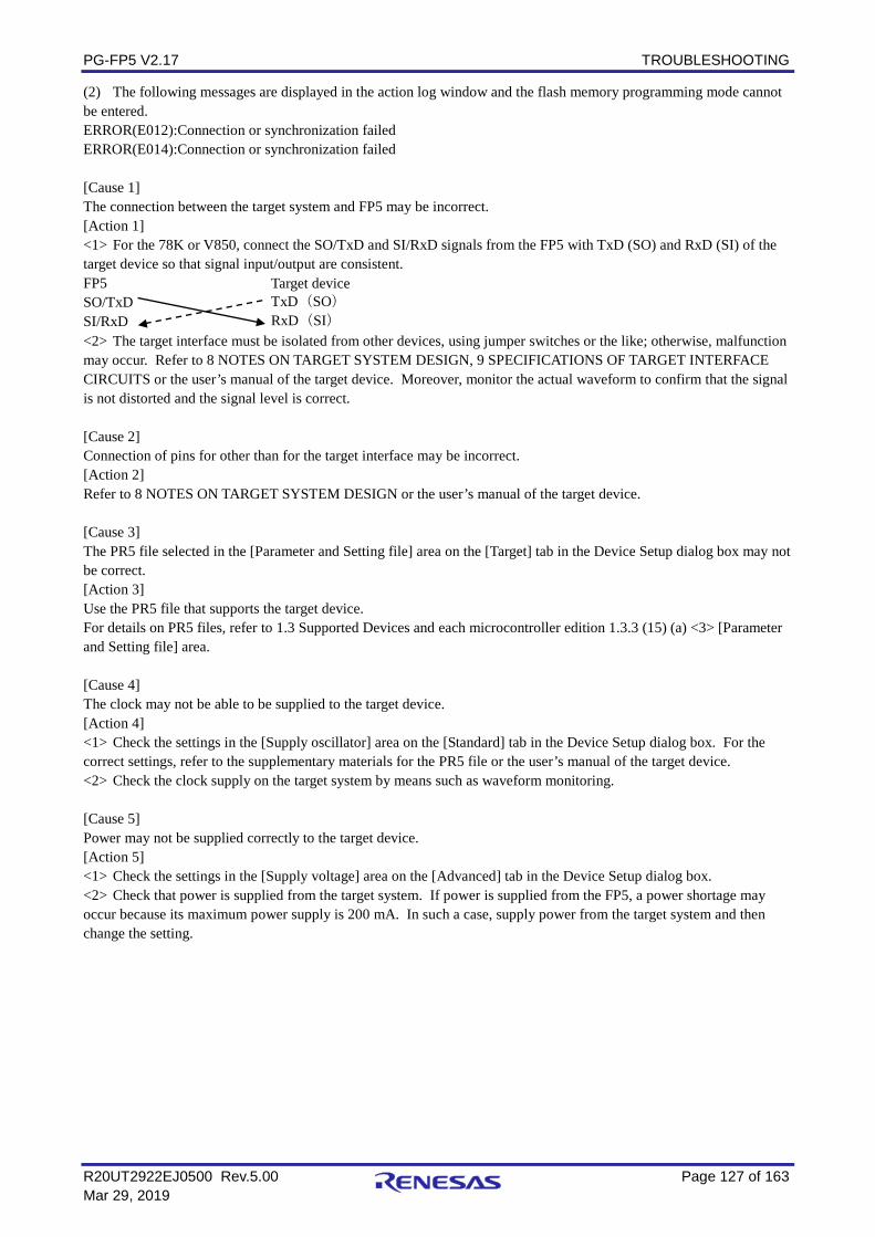
PG-FP5 V2.17 TROUBLESHOOTING
R20UT2922EJ0500 Rev.5.00 Page 127 of 163 Mar 29, 2019
(2) The following messages are displayed in the action log window and the flash memory programming mode cannot be entered. ERROR(E012):Connection or synchronization failed ERROR(E014):Connection or synchronization failed [Cause 1] The connection between the target system and FP5 may be incorrect. [Action 1] <1> For the 78K or V850, connect the SO/TxD and SI/RxD signals from the FP5 with TxD (SO) and RxD (SI) of the target device so that signal input/output are consistent.
<2> The target interface must be isolated from other devices, using jumper switches or the like; otherwise, malfunction may occur. Refer to 8 NOTES ON TARGET SYSTEM DESIGN, 9 SPECIFICATIONS OF TARGET INTERFACE CIRCUITS or the user’s manual of the target device. Moreover, monitor the actual waveform to confirm that the signal is not distorted and the signal level is correct. [Cause 2] Connection of pins for other than for the target interface may be incorrect. [Action 2] Refer to 8 NOTES ON TARGET SYSTEM DESIGN or the user’s manual of the target device. [Cause 3] The PR5 file selected in the [Parameter and Setting file] area on the [Target] tab in the Device Setup dialog box may not be correct. [Action 3] Use the PR5 file that supports the target device. For details on PR5 files, refer to 1.3 Supported Devices and each microcontroller edition 1.3.3 (15) (a) <3> [Parameter and Setting file] area. [Cause 4] The clock may not be able to be supplied to the target device. [Action 4] <1> Check the settings in the [Supply oscillator] area on the [Standard] tab in the Device Setup dialog box. For the correct settings, refer to the supplementary materials for the PR5 file or the user’s manual of the target device. <2> Check the clock supply on the target system by means such as waveform monitoring. [Cause 5] Power may not be supplied correctly to the target device. [Action 5] <1> Check the settings in the [Supply voltage] area on the [Advanced] tab in the Device Setup dialog box. <2> Check that power is supplied from the target system. If power is supplied from the FP5, a power shortage may occur because its maximum power supply is 200 mA. In such a case, supply power from the target system and then change the setting.
FP5 SO/TxD SI/RxD
Target device TxD(SO) RxD(SI)
PG-FP5 V2.17 TROUBLESHOOTING
R20UT2922EJ0500 Rev.5.00 Page 128 of 163 Mar 29, 2019
[Cause 6] UART communication may not be synchronized. [Action 6] When UART is used, communication may not be synchronized due to a baud rate error of the target device. In this case, change the CPU clock or baud rate, or change the communication channel to another communication mode. [Cause 7] If using a 78K0S/Kx1+ microcontroller or the UPD78F9334, it is possible that the wrong connection procedure was implemented. [Action 7] With devices that using program files in which “use the RESET¯¯¯¯¯¯ pin as the input-only port (P34)” is set by the option byte, flash memory programming mode cannot be entered if power is supplied to the target system before the target cable is connected to the target system. Connect the target cable to the target system and then supply power to the target system as prescribed in the connection procedure. [Cause 8] For the RX family and Super H family, the I/O signal setting does not match the wiring of the target system. [Action 8] Check if the settings in the [I/O Signal Settings] area on the [Advanced] tab in the Device Setup dialog box match the wiring of the target system. (3) The following message is displayed in the action log window and normal communication is not performed in flash memory programming mode. ERROR Communication failure or timeout. [Cause 1] The clock or power supply may not be stable. [Action 1] Confirm that the clock or power is supplied on the target system. [Cause 2] Communication may not be stable. [Action 2] <1> Confirm that no noise is applied to communication. <2> Confirm that the FP5 and target system are properly connected. <3> Confirm that unused pins are properly handled. <4> Confirm that an appropriate clock and communication rate are selected. Stable programming may be achieved by setting a lower value for the clock or communication rate.
PG-FP5 V2.17 MAINTENANCE AND WARRANTY
R20UT2922EJ0500 Rev.5.00 Page 129 of 163 Mar 29, 2019
11. MAINTENANCE AND WARRANTY This chapter covers basic maintenance, warranty information, provisions for repair and the procedures for requesting a repair. 11.1. Maintenance (1) If dust or dirt collects on this product, wipe it off with a dry soft cloth. Do not use thinner or other solvents because these chemicals can cause the surface coating to separate. (2) When you do not use this product for a long period, disconnect it from the power supply, host PC and user system. 11.2. Warranty (1) This product comes with a one-year warranty after purchase. Should the product break down or be damaged while you’re using it under normal condition based on its user’s manual, it will be repaired or replaced free of cost. (2) However, if the following failure or damage occurs to the product under warranty, the product will be repaired or replaced at cost. a) Failure or damage attributable to the misuse or abuse of the product or its use under other abnormal conditions. b) Failure or damage attributable to improper handling of the product after purchase, such as dropping of the product when it is transported or moved. c) Failure or damage to the product caused by other pieces of equipment connected to it. d) Failure or damage attributable to fire, earthquakes, thunderbolts, floods, or other natural disasters or abnormal voltages, etc. e) Failure or damage attributable to modifications, repairs, adjustments, or other acts made to the product by other than Renesas Electronics Corporation. (3) Consumables (e.g., sockets and adapters) are not covered by the aforementioned repair. In the above cases, contact your local distributor. If your product is being leased, consult the leasing company or the owner. 11.3. Repair Provisions (1) Repairs not covered by warranty Problems arising in products for which more than one year has elapsed since purchase are not covered by warranty. (2) Replacement not covered by warranty If your product's fault falls into any of the following categories, the fault will be corrected by replacing the entire product instead of repairing it, or you will be advised to purchase a new product, depending on the severity of the fault. - Faulty or broken mechanical portions - Flaws, separation, or rust in coated or plated portions - Flaws or cracks in plastic portions - Faults or breakage caused by improper use or unauthorized repair or modification - Heavily damaged electric circuits due to overvoltage, overcurrent or shorting of power supply - Cracks in the printed circuit board or burnt-down patterns - A wide range of faults that make replacement less expensive than repair - Faults that are not locatable or identifiable (3) Expiration of the repair period When a period of one year has elapsed after production of a given model ceased, repairing products of that model may become impossible. (4) Carriage fees for sending your product to be repaired Carriage fees for sending your product to us for repair are at your own expense.
PG-FP5 V2.17 MAINTENANCE AND WARRANTY
R20UT2922EJ0500 Rev.5.00 Page 130 of 163 Mar 29, 2019
11.4. How to Make Request for Repair If your product is found faulty, fill in a Repair Request Sheet downloadable from the following URL. And email the sheet and send the product to your local distributor. https://www.renesas.com/repair
CAUTION Note on Transporting the Product:
When sending your product for repair, use the packing box and cushioning material supplied with the product when it was delivered to you and specify caution in handling (handling as precision equipment). If packing of your product is not complete, it may be damaged during transportation. When you pack your product in a bag, make sure to use the conductive plastic bag supplied with the product (usually a blue bag). If you use a different bag, it may lead to further trouble with your product due to static electricity.
PG-FP5 V2.17 MESSAGES
R20UT2922EJ0500 Rev.5.00 Page 131 of 163 Mar 29, 2019
APPENDIX A MESSAGES This chapter explains the messages. A.1. Message Format Messages will be output in the error/warning dialog boxes, information dialog boxes, or action log window during programming GUI operation. Error messages will be displayed on the FP5 message display during standalone operation.
Figure A.1 Error/Warning Dialog Box
Figure A.2 Information Dialog Box
Figure A.3 Action Log Window
Figure A.4 Error Message FP5 Message Display
ERROR: 012 Synchron. failed
PG-FP5 V2.17 MESSAGES
R20UT2922EJ0500 Rev.5.00 Page 132 of 163 Mar 29, 2019
A.2. Error/Warning Dialog Boxes for Programming GUI Operation (1)
No. Message Description E 1100 Communication within host PC and
FlashProgrammer is broken An error occurred in communication between the host PC and the FP5. Check the cable connection and FP5 power supply.
E 1101 Can't setup communication within host PC and FlashProgrammer
Communication between the host PC and FP5 cannot be established. Check the cable connection and power supply. Moreover, check if the USB driver is installed correctly.
E 1102 Can't find parameter file The specified PR5 file could not be found.
E 1103 Open parameter file failed The specified PR5 file cannot be opened.
E 1105 Wrong FPGA Version detected! Please update to FPGA Vx, otherwise FP5 function may fail.
Wrong FPGA Version detected! Please update to FPGA of the displayed version.
E 1106 Firmware is not valid or version is lower than requirement.
Incorrect version information or an old version was detected. Update the FP5 firmware.
E 1107 Parameter area format is not match with initial file. Do you want reset parameter area format?
The factor for dividing the programming area does not match the one defined in the INI file. Select whether to reset the division factor. If reset, it is divided into four areas and the contents are deleted.
E 1108 No invalid Parameter file defined. GUI can not work properly.
The GUI will not operate normally because no valid PR5 file has been defined. Set it in the Device Setup dialog box.
E 1109 No parameter file exists in this project folder. Please select parameter files.
There is no parameter file in user selected folder. GUI waited user to find out one or more parameter files in other folder.
E 1201 Invalid file. The specified file cannot be opened. Set it in the Device Setup dialog box.
E 1202 <Setting file name> is not valid. Using most recent settings.
An incorrect format or value was detected in the ESF file. The ESF file defined in the INI file will be used instead. Set it in the Device Setup dialog box.
E 1203 <Parameter file name> is not valid. Using most recent settings.
An incorrect format or value was detected in the PR5 file. The ESF file defined in the INI file will be used instead. Set it in the Device Setup dialog box.
E 1204 Download of parameter file failed. Downloading of the PR5 file has failed. The PR5 file may be invalid. Re-set the connection between the host PC and FP5.
E 1205 Download of setting file failed. Downloading of the ESF file has failed. The ESF file may be invalid. Re-set the connection between the host PC and FP5.
E 1206 File name is not valid. The specified file cannot be opened for writing. Make sure that the file attribute is not set to read-only.
E 1400 Password is invalid. Effective password consists one to eight any alphanumeric character. It is case insensitive.
Password contains invalid character or out of size range.
E 1401 The password does not match. [Yes]: Retry to input the password [No]: Initialize the password and format to the shipment condition.
Password is different with defined content.
PG-FP5 V2.17 MESSAGES
R20UT2922EJ0500 Rev.5.00 Page 133 of 163 Mar 29, 2019
(2) No. Message Description
E 1501 This file is not valid. The file opened with the HEX Editor is invalid.
E 1502 Caution: Data Flash access unit is DWORD. The data flash area can be accessed in double-word units, but an access was attempted in unsupported units.
E 1503 Caution: Out of range! The address range for saving data is out of the code flash or data flash address range. Check the start/end address.
E 1504 Caution: Start address should not larger than End address.
The start address is larger than the end address. Check the start/end address.
E 1505 Caution: End address should not smaller than start address.
The end address is smaller than the start address. Check the start/end address.
E 1506 The file cannot be read. The file opened with the HEX Editor is invalid.
E 1507 No HEX data. The program file format may be incorrect.
E 1508 The file cannot be written. Saving of the program file has failed. Check if this file is occupied by another program.
E 1509 Temporary file could not be created.Abort The temporary file cannot be created. Creation was aborted. Confirm that sufficient memory capacity is available in Windows.
E 1510 Can not open <file name> Abort <file-name> cannot be opened.
E 1511 File load error. Abort An error occurred during file reading or writing.
E 1512 Memory cannot be allocated. Confirm that sufficient memory capacity is available in Windows.
E 1513 Memory reallocation error Confirm that sufficient memory capacity is available in Windows.
E 1514 Check sum error. Continue? It was detected that the checksum of the program file opened by the HEX editor was invalid. Click OK to continue checksum verification. Click Cancel to abort checksum verification.
E 1515 Cannot open <file name> Abort. The program file specified by the HEX editor cannot be opened.
E 1516 Error line : <line number> Data error. Abort DATA Check
An illegal data exists in line line-number in the program file.
E 1517 Shortage of memory. Confirm that sufficient memory capacity is available in Windows.
E 1518 Invalid file name. The file name is invalid.
E 1519 HEX format error. An illegal program file format was detected.
E 1520 Too large address. The address is too large. The maximum address that can be used by the HEX Editor is 420000h.
E 1521 Can not run <command name> Running of the command-name command has failed.
E 1522 Illegal address The range of the data storage address is invalid. The start address may be larger than the end address.
E 1523 <file name> could not be opened. Abort Save File <file-name> cannot be opened. File saving was aborted.
E 1524 Data error. Abort DATA Check A data error has been found in the program file. Data checking was aborted.
E 1525 Temporary file could not be read. Abort Save File Opening of the temporary file has failed. The file may be corrupted.
PG-FP5 V2.17 MESSAGES
R20UT2922EJ0500 Rev.5.00 Page 134 of 163 Mar 29, 2019
(3) No. Message Description
E 1526 Error line : <line number> Data Count error. Abort "Data Count Check"
A data count error has occurred in line line-number. The program file format may be incorrect.
E 1527 Cannot open temporary file. Opening of the temporary file has failed. The file may be corrupted.
E 1528 File Save error. Abort "Save File" Saving the file has failed.
E 1529 <line number> Check sum error. Continue ? A checksum error has occurred in line line-number. The program file format may be incorrect. Select whether to continue the operation.
E 1530 Too large address. Edit range: 0 - 0x420000 The program file address is too large. Set an address value in the range 0 to 420000h.
E 1531 Data Flash format error: <data address>: Invalid ID Tag.
The data flash format is invalid. Valid 4 bytes are followed by an ID tag of 4-byte FFh or 4-byte 00h in the data flash area. An error occurs if the ID tag includes defects, or FFh or 00h is included.
E 1532 Parameter of "Start Address" is invalid. The value input as the start address is not a valid hexadecimal number.
E 1533 Parameter of "End Address" is invalid. The value input as the end address is not a valid hexadecimal number.
E 1534 Temporary file could not be read. Abort Dump Hex The temporary file cannot be read. Opening of the HEX Editor was aborted.
E 1535 Can not open <file name> Abort 'Dump Hex' <file-name> cannot be opened. Opening of the HEX Editor was aborted.
E 1536 File load error. Abort 'Dump Hex' A file load error. Opening of the HEX Editor was aborted.
E 1537 Error line : <line number > Check sum error. Abort "Check sum" Check
An incorrect checksum was detected in line line-number in the program file. The program file format may be incorrect.
E 1538 Can not read temporary file. Reading of the temporary file has failed. The file may be corrupted.
E 1539 Caution: Out of range! The specified value is out of the valid range.
E 1540 Caution: Failed input! Input area is empty.
E 1601 Protect error. The on-chip debug security ID and option byte settings cannot be read because read-prohibited has been specified.
E 1604 Invallid address found in HEX file: <file name >This file can not be used with command option 'minimum unit programming'
Message occurred when address defined in HEX file is out of range of parameter file defined.
E 1605 Invallid HEX file: <file name >This file can not be used with command option 'minimum unit programming'
Message occurred when HEX file has not valid. E.g. Wrong checksum or wrong data format inside HEX file.
E 1801 Checksum error in program file! Confirm the selected program file.
E 1802 Overlap error in program file! Confirm the selected program file.
E 1803 Format error in program file! Confirm the selected program file.
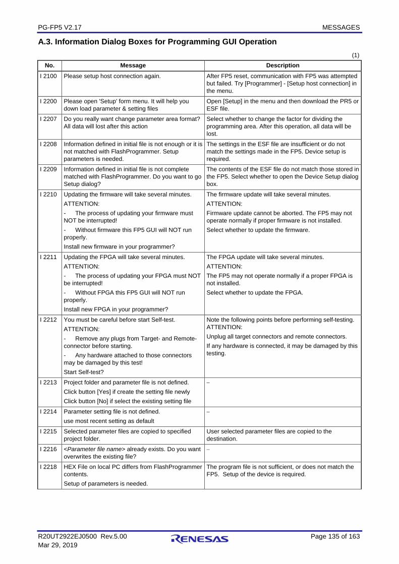
PG-FP5 V2.17 MESSAGES
R20UT2922EJ0500 Rev.5.00 Page 135 of 163 Mar 29, 2019
A.3. Information Dialog Boxes for Programming GUI Operation (1)
No. Message Description I 2100 Please setup host connection again. After FP5 reset, communication with FP5 was attempted
but failed. Try [Programmer] - [Setup host connection] in the menu.
I 2200 Please open 'Setup' form menu. It will help you down load parameter & setting files
Open [Setup] in the menu and then download the PR5 or ESF file.
I 2207 Do you really want change parameter area format? All data will lost after this action
Select whether to change the factor for dividing the programming area. After this operation, all data will be lost.
I 2208 Information defined in initial file is not enough or it is not matched with FlashProgrammer. Setup parameters is needed.
The settings in the ESF file are insufficient or do not match the settings made in the FP5. Device setup is required.
I 2209 Information defined in initial file is not complete matched with FlashProgrammer. Do you want to go Setup dialog?
The contents of the ESF file do not match those stored in the FP5. Select whether to open the Device Setup dialog box.
I 2210 Updating the firmware will take several minutes. ATTENTION: - The process of updating your firmware must NOT be interrupted! - Without firmware this FP5 GUI will NOT run properly. Install new firmware in your programmer?
The firmware update will take several minutes. ATTENTION: Firmware update cannot be aborted. The FP5 may not operate normally if proper firmware is not installed. Select whether to update the firmware.
I 2211 Updating the FPGA will take several minutes. ATTENTION: - The process of updating your FPGA must NOT be interrupted! - Without FPGA this FP5 GUI will NOT run properly. Install new FPGA in your programmer?
The FPGA update will take several minutes. ATTENTION: The FP5 may not operate normally if a proper FPGA is not installed. Select whether to update the FPGA.
I 2212 You must be careful before start Self-test. ATTENTION: - Remove any plugs from Target- and Remote-connector before starting. - Any hardware attached to those connectors may be damaged by this test! Start Self-test?
Note the following points before performing self-testing. ATTENTION: Unplug all target connectors and remote connectors. If any hardware is connected, it may be damaged by this testing.
I 2213 Project folder and parameter file is not defined. Click button [Yes] if create the setting file newly Click button [No] if select the existing setting file
−
I 2214 Parameter setting file is not defined. use most recent setting as default
−
I 2215 Selected parameter files are copied to specified project folder.
User selected parameter files are copied to the destination.
I 2216 <Parameter file name> already exists. Do you want overwrites the existing file?
−
I 2218 HEX File on local PC differs from FlashProgrammer contents. Setup of parameters is needed.
The program file is not sufficient, or does not match the FP5. Setup of the device is required.
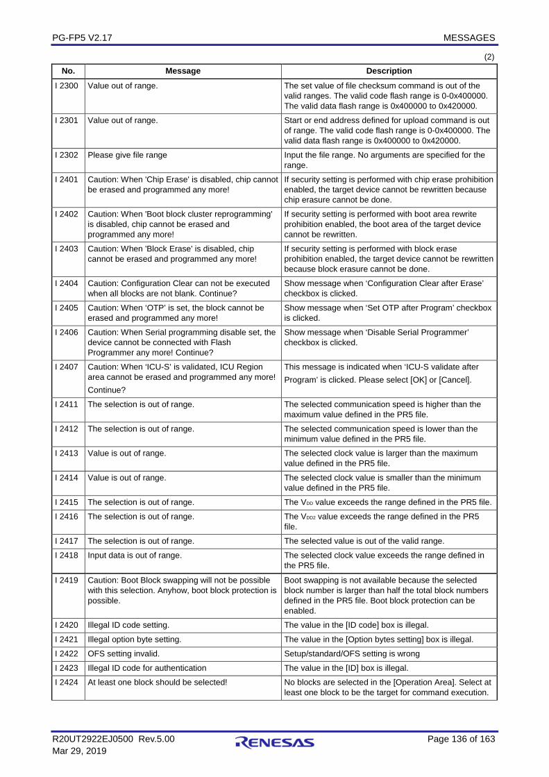
PG-FP5 V2.17 MESSAGES
R20UT2922EJ0500 Rev.5.00 Page 136 of 163 Mar 29, 2019
(2) No. Message Description
I 2300 Value out of range. The set value of file checksum command is out of the valid ranges. The valid code flash range is 0-0x400000. The valid data flash range is 0x400000 to 0x420000.
I 2301 Value out of range. Start or end address defined for upload command is out of range. The valid code flash range is 0-0x400000. The valid data flash range is 0x400000 to 0x420000.
I 2302 Please give file range Input the file range. No arguments are specified for the range.
I 2401 Caution: When 'Chip Erase' is disabled, chip cannot be erased and programmed any more!
If security setting is performed with chip erase prohibition enabled, the target device cannot be rewritten because chip erasure cannot be done.
I 2402 Caution: When 'Boot block cluster reprogramming' is disabled, chip cannot be erased and programmed any more!
If security setting is performed with boot area rewrite prohibition enabled, the boot area of the target device cannot be rewritten.
I 2403 Caution: When 'Block Erase' is disabled, chip cannot be erased and programmed any more!
If security setting is performed with block erase prohibition enabled, the target device cannot be rewritten because block erasure cannot be done.
I 2404 Caution: Configuration Clear can not be executed when all blocks are not blank. Continue?
Show message when ‘Configuration Clear after Erase’ checkbox is clicked.
I 2405 Caution: When ‘OTP’ is set, the block cannot be erased and programmed any more!
Show message when ‘Set OTP after Program’ checkbox is clicked.
I 2406 Caution: When Serial programming disable set, the device cannot be connected with Flash Programmer any more! Continue?
Show message when ‘Disable Serial Programmer’ checkbox is clicked.
I 2407 Caution: When ‘ICU-S’ is validated, ICU Region area cannot be erased and programmed any more! Continue?
This message is indicated when ‘ICU-S validate after Program’ is clicked. Please select [OK] or [Cancel].
I 2411 The selection is out of range. The selected communication speed is higher than the maximum value defined in the PR5 file.
I 2412 The selection is out of range. The selected communication speed is lower than the minimum value defined in the PR5 file.
I 2413 Value is out of range. The selected clock value is larger than the maximum value defined in the PR5 file.
I 2414 Value is out of range. The selected clock value is smaller than the minimum value defined in the PR5 file.
I 2415 The selection is out of range. The VDD value exceeds the range defined in the PR5 file.
I 2416 The selection is out of range. The VDD2 value exceeds the range defined in the PR5 file.
I 2417 The selection is out of range. The selected value is out of the valid range.
I 2418 Input data is out of range. The selected clock value exceeds the range defined in the PR5 file.
I 2419 Caution: Boot Block swapping will not be possible with this selection. Anyhow, boot block protection is possible.
Boot swapping is not available because the selected block number is larger than half the total block numbers defined in the PR5 file. Boot block protection can be enabled.
I 2420 Illegal ID code setting. The value in the [ID code] box is illegal.
I 2421 Illegal option byte setting. The value in the [Option bytes setting] box is illegal.
I 2422 OFS setting invalid. Setup/standard/OFS setting is wrong
I 2423 Illegal ID code for authentication The value in the [ID] box is illegal.
I 2424 At least one block should be selected! No blocks are selected in the [Operation Area]. Select at least one block to be the target for command execution.
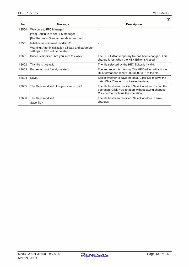
PG-FP5 V2.17 MESSAGES
R20UT2922EJ0500 Rev.5.00 Page 137 of 163 Mar 29, 2019
(3) No. Message Description
I 2500 Welcome to FP5 Manager! [Yes]:Continue to set FP5 Manager [No]:Return to Standard mode unsecured
−
I 2501 Initialize as shipment condition? Warning: After initialization all data and parameter settings in FP5 will be deleted.
−
I 2601 Buffer is modified. Are you sure to close? The HEX Editor temporary file has been changed. This change is lost when the HEX Editor is closed.
I 2602 This file is not valid. The file selected by the HEX Editor is invalid.
I 2603 End record not found, created. The end record is missing. The HEX editor will add the HEX format end record ':00000001FF' to the file.
I 2604 Save? Select whether to save the data. Click 'Ok' to save the data. Click 'Cancel' to not save the data.
I 2605 The file is modified. Are you sure to quit? The file has been modified. Select whether to abort the operation. Click 'Yes' to abort without saving changes. Click 'No' to continue the operation.
I 2606 The file is modified. Save file?
The file has been modified. Select whether to save changes.
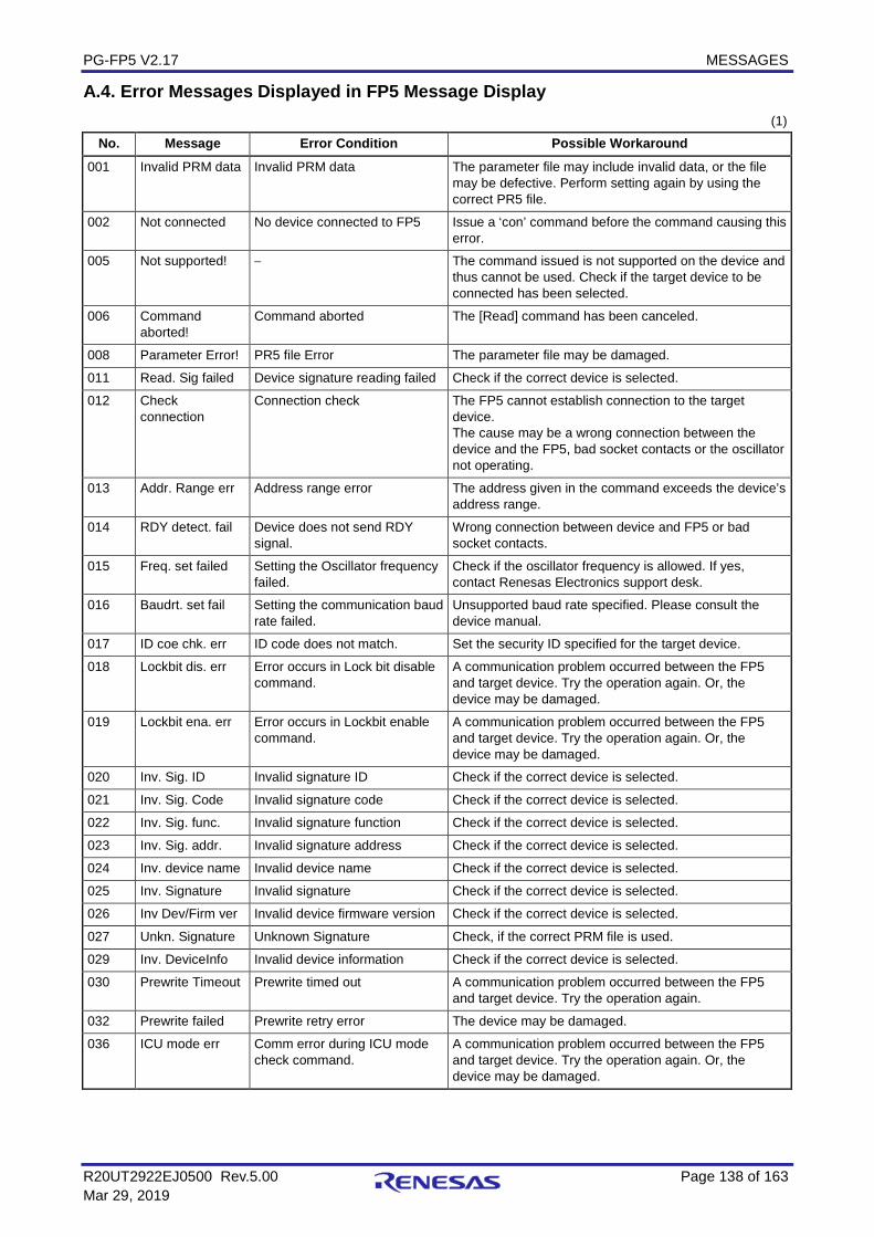
PG-FP5 V2.17 MESSAGES
R20UT2922EJ0500 Rev.5.00 Page 138 of 163 Mar 29, 2019
A.4. Error Messages Displayed in FP5 Message Display (1)
No. Message Error Condition Possible Workaround 001 Invalid PRM data Invalid PRM data The parameter file may include invalid data, or the file
may be defective. Perform setting again by using the correct PR5 file.
002 Not connected No device connected to FP5 Issue a ‘con’ command before the command causing this error.
005 Not supported! − The command issued is not supported on the device and thus cannot be used. Check if the target device to be connected has been selected.
006 Command aborted!
Command aborted The [Read] command has been canceled.
008 Parameter Error! PR5 file Error The parameter file may be damaged.
011 Read. Sig failed Device signature reading failed Check if the correct device is selected.
012 Check connection
Connection check The FP5 cannot establish connection to the target device. The cause may be a wrong connection between the device and the FP5, bad socket contacts or the oscillator not operating.
013 Addr. Range err Address range error The address given in the command exceeds the device’s address range.
014 RDY detect. fail Device does not send RDY signal.
Wrong connection between device and FP5 or bad socket contacts.
015 Freq. set failed Setting the Oscillator frequency failed.
Check if the oscillator frequency is allowed. If yes, contact Renesas Electronics support desk.
016 Baudrt. set fail Setting the communication baud rate failed.
Unsupported baud rate specified. Please consult the device manual.
017 ID coe chk. err ID code does not match. Set the security ID specified for the target device.
018 Lockbit dis. err Error occurs in Lock bit disable command.
A communication problem occurred between the FP5 and target device. Try the operation again. Or, the device may be damaged.
019 Lockbit ena. err Error occurs in Lockbit enable command.
A communication problem occurred between the FP5 and target device. Try the operation again. Or, the device may be damaged.
020 Inv. Sig. ID Invalid signature ID Check if the correct device is selected.
021 Inv. Sig. Code Invalid signature code Check if the correct device is selected.
022 Inv. Sig. func. Invalid signature function Check if the correct device is selected.
023 Inv. Sig. addr. Invalid signature address Check if the correct device is selected.
024 Inv. device name Invalid device name Check if the correct device is selected.
025 Inv. Signature Invalid signature Check if the correct device is selected.
026 Inv Dev/Firm ver Invalid device firmware version Check if the correct device is selected.
027 Unkn. Signature Unknown Signature Check, if the correct PRM file is used.
029 Inv. DeviceInfo Invalid device information Check if the correct device is selected.
030 Prewrite Timeout Prewrite timed out A communication problem occurred between the FP5 and target device. Try the operation again.
032 Prewrite failed Prewrite retry error The device may be damaged.
036 ICU mode err Comm error during ICU mode check command.
A communication problem occurred between the FP5 and target device. Try the operation again. Or, the device may be damaged.
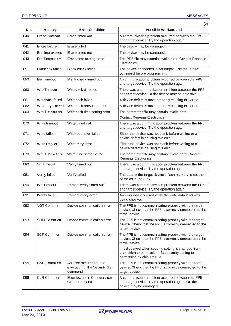
PG-FP5 V2.17 MESSAGES
R20UT2922EJ0500 Rev.5.00 Page 139 of 163 Mar 29, 2019
(2) No. Message Error Condition Possible Workaround
040 Erase Timeout Erase timed out A communication problem occurred between the FP5 and target device. Try the operation again.
041 Erase failure Erase failed The device may be damaged.
042 Ers time exceed Erase timed out The device may be damaged.
043 Ers Timeset err Erase time setting error The PR5 file may contain invalid data. Contact Renesas Electronics.
051 Blank chk failed Blank check failed The device connected is not empty. Use the ‘erase’ command before programming.
050 Bln Timeout Blank check timed out A communication problem occurred between the FP5 and target device. Try the operation again.
060 Wrb Timeout Writeback timed out There was a communication problem between the FP5 and target device. Or the device may be defective.
061 Writeback failed Writeback failed A device defect is most probably causing this error.
062 Wrb retry exceed Writeback retry timed out A device defect is most probably causing this error.
063 Wrb Timeset err Writeback time setting error The parameter file may contain invalid data. Contact Renesas Electronics.
070 Write timeout Write timed out There was a communication problem between the FP5 and target device. Try the operation again.
071 Write failed Write operation failed Either the device was not blank before writing or a device defect is causing this error.
072 Write retry err Write retry error Either the device was not blank before writing or a device defect is causing this error.
073 Wrt. Timeset err Write time setting error The parameter file may contain invalid data. Contact Renesas Electronics.
080 Vrf Timeout Verify timed out There was a communication problem between the FP5 and target device. Try the operation again.
081 Verify failed Verify failed The data in the target device’s flash memory is not the same as in the FP5.
090 IVrf Timeout Internal verify timed out There was a communication problem between the FP5 and target device. Try the operation again.
091 IVerify failed Internal verify error An error was occurred while the write data level was being checked.
092 VGT Comm err Device communication error The FP5 is not communicating properly with the target device. Check that the FP5 is correctly connected to the target device.
093 SUM Comm err Device communication error The FP5 is not communicating properly with the target device. Check that the FP5 is correctly connected to the target device.
094 SCF Comm err Device communication error The FP5 is not communicating properly with the target device. Check that the FP5 is correctly connected to the target device. It is displayed when security setting is changed from prohibition to permission. Set security setting to permission by chip erasure.
095 GSC Comm err An error occurred during execution of the Security Get command
The FP5 is not communicating properly with the target device. Check that the FP5 is correctly connected to the target device.
096 CLR Comm err Error occurs in Configuration Clear command.
A communication problem occurred between the FP5 and target device. Try the operation again. Or, the device may be damaged.
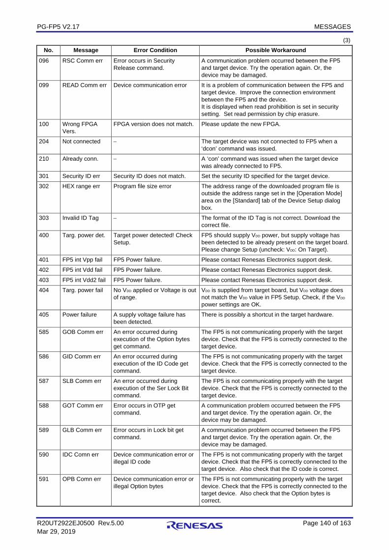
PG-FP5 V2.17 MESSAGES
R20UT2922EJ0500 Rev.5.00 Page 140 of 163 Mar 29, 2019
(3) No. Message Error Condition Possible Workaround
096 RSC Comm err Error occurs in Security Release command.
A communication problem occurred between the FP5 and target device. Try the operation again. Or, the device may be damaged.
099 READ Comm err Device communication error It is a problem of communication between the FP5 and target device. Improve the connection environment between the FP5 and the device. It is displayed when read prohibition is set in security setting. Set read permission by chip erasure.
100 Wrong FPGA Vers.
FPGA version does not match. Please update the new FPGA.
204 Not connected − The target device was not connected to FP5 when a ‘dcon’ command was issued.
210 Already conn. − A ‘con’ command was issued when the target device was already connected to FP5.
301 Security ID err Security ID does not match. Set the security ID specified for the target device.
302 HEX range err Program file size error The address range of the downloaded program file is outside the address range set in the [Operation Mode] area on the [Standard] tab of the Device Setup dialog box.
303 Invalid ID Tag − The format of the ID Tag is not correct. Download the correct file.
400 Targ. power det. Target power detected! Check Setup.
FP5 should supply VDD power, but supply voltage has been detected to be already present on the target board. Please change Setup (uncheck: VDD: On Target).
401 FP5 int Vpp fail FP5 Power failure. Please contact Renesas Electronics support desk.
402 FP5 int Vdd fail FP5 Power failure. Please contact Renesas Electronics support desk.
403 FP5 int Vdd2 fail FP5 Power failure. Please contact Renesas Electronics support desk.
404 Targ. power fail No VDD applied or Voltage is out of range.
VDD is supplied from target board, but VDD voltage does not match the VDD value in FP5 Setup. Check, if the VDD power settings are OK.
405 Power failure A supply voltage failure has been detected.
There is possibly a shortcut in the target hardware.
585 GOB Comm err An error occurred during execution of the Option bytes get command.
The FP5 is not communicating properly with the target device. Check that the FP5 is correctly connected to the target device.
586 GID Comm err An error occurred during execution of the ID Code get command.
The FP5 is not communicating properly with the target device. Check that the FP5 is correctly connected to the target device.
587 SLB Comm err An error occurred during execution of the Ser Lock Bit command.
The FP5 is not communicating properly with the target device. Check that the FP5 is correctly connected to the target device.
588 GOT Comm err Error occurs in OTP get command.
A communication problem occurred between the FP5 and target device. Try the operation again. Or, the device may be damaged.
589 GLB Comm err Error occurs in Lock bit get command.
A communication problem occurred between the FP5 and target device. Try the operation again. Or, the device may be damaged.
590 IDC Comn err Device communication error or illegal ID code
The FP5 is not communicating properly with the target device. Check that the FP5 is correctly connected to the target device. Also check that the ID code is correct.
591 OPB Comn err Device communication error or illegal Option bytes
The FP5 is not communicating properly with the target device. Check that the FP5 is correctly connected to the target device. Also check that the Option bytes is correct.
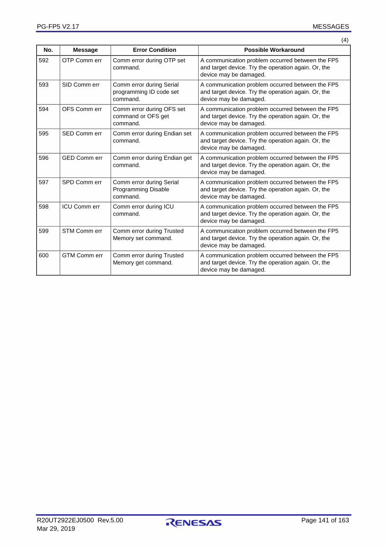
PG-FP5 V2.17 MESSAGES
R20UT2922EJ0500 Rev.5.00 Page 141 of 163 Mar 29, 2019
(4) No. Message Error Condition Possible Workaround
592 OTP Comm err Comm error during OTP set command.
A communication problem occurred between the FP5 and target device. Try the operation again. Or, the device may be damaged.
593 SID Comm err Comm error during Serial programming ID code set command.
A communication problem occurred between the FP5 and target device. Try the operation again. Or, the device may be damaged.
594 OFS Comm err Comm error during OFS set command or OFS get command.
A communication problem occurred between the FP5 and target device. Try the operation again. Or, the device may be damaged.
595 SED Comm err Comm error during Endian set command.
A communication problem occurred between the FP5 and target device. Try the operation again. Or, the device may be damaged.
596 GED Comm err Comm error during Endian get command.
A communication problem occurred between the FP5 and target device. Try the operation again. Or, the device may be damaged.
597 SPD Comm err Comm error during Serial Programming Disable command.
A communication problem occurred between the FP5 and target device. Try the operation again. Or, the device may be damaged.
598 ICU Comm err Comm error during ICU command.
A communication problem occurred between the FP5 and target device. Try the operation again. Or, the device may be damaged.
599 STM Comm err Comm error during Trusted Memory set command.
A communication problem occurred between the FP5 and target device. Try the operation again. Or, the device may be damaged.
600 GTM Comm err Comm error during Trusted Memory get command.
A communication problem occurred between the FP5 and target device. Try the operation again. Or, the device may be damaged.
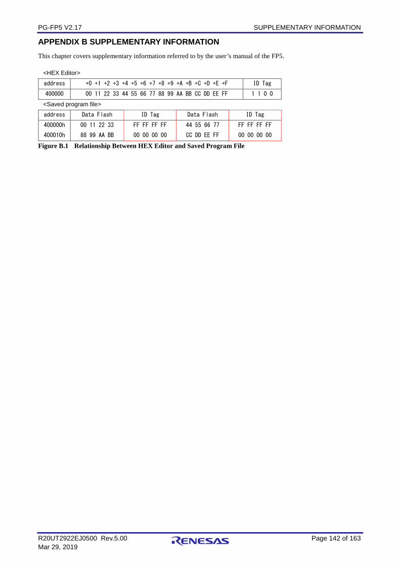
PG-FP5 V2.17 SUPPLEMENTARY INFORMATION
R20UT2922EJ0500 Rev.5.00 Page 142 of 163 Mar 29, 2019
APPENDIX B SUPPLEMENTARY INFORMATION This chapter covers supplementary information referred to by the user’s manual of the FP5.
<HEX Editor>
address +0 +1 +2 +3 +4 +5 +6 +7 +8 +9 +A +B +C +D +E +F ID Tag
400000 00 11 22 33 44 55 66 77 88 99 AA BB CC DD EE FF 1 1 0 0
<Saved program file>
address Data Flash ID Tag Data Flash ID Tag
400000h 00 11 22 33 FF FF FF FF 44 55 66 77 FF FF FF FF
400010h 88 99 AA BB 00 00 00 00 CC DD EE FF 00 00 00 00
Figure B.1 Relationship Between HEX Editor and Saved Program File
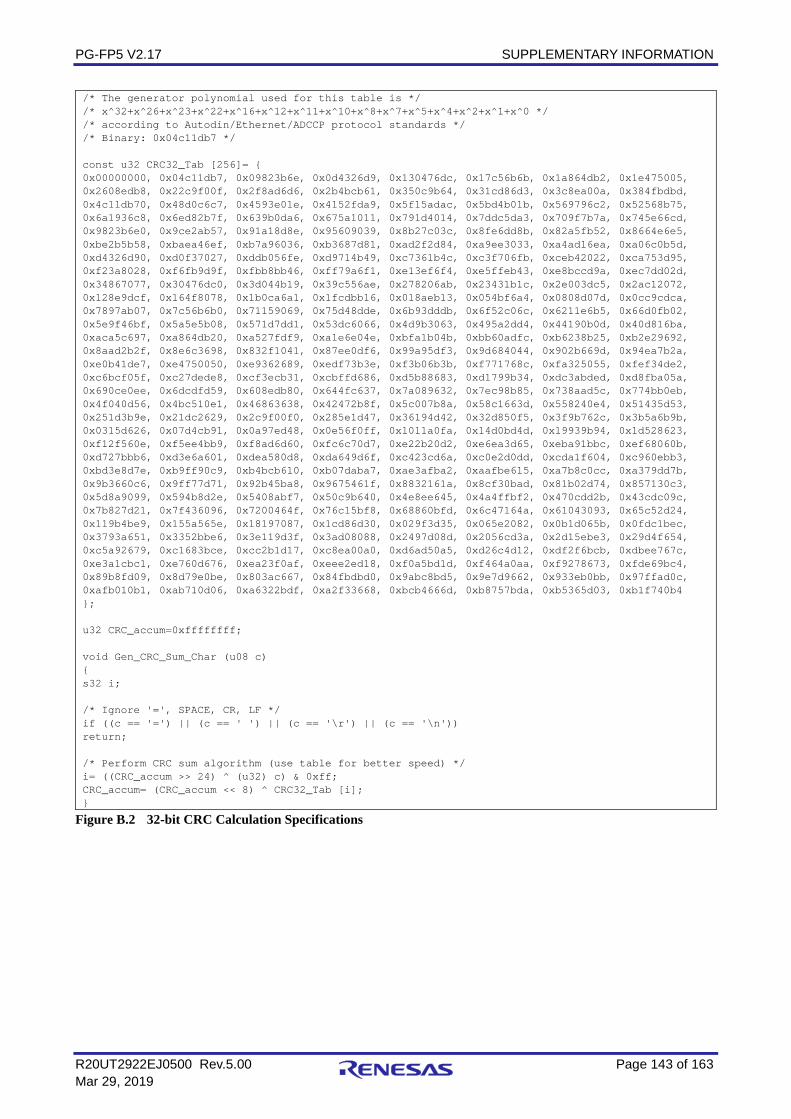
PG-FP5 V2.17 SUPPLEMENTARY INFORMATION
R20UT2922EJ0500 Rev.5.00 Page 143 of 163 Mar 29, 2019
/* The generator polynomial used for this table is */ /* x^32+x^26+x^23+x^22+x^16+x^12+x^11+x^10+x^8+x^7+x^5+x^4+x^2+x^1+x^0 */ /* according to Autodin/Ethernet/ADCCP protocol standards */ /* Binary: 0x04c11db7 */ const u32 CRC32_Tab [256]= 0x00000000, 0x04c11db7, 0x09823b6e, 0x0d4326d9, 0x130476dc, 0x17c56b6b, 0x1a864db2, 0x1e475005, 0x2608edb8, 0x22c9f00f, 0x2f8ad6d6, 0x2b4bcb61, 0x350c9b64, 0x31cd86d3, 0x3c8ea00a, 0x384fbdbd, 0x4c11db70, 0x48d0c6c7, 0x4593e01e, 0x4152fda9, 0x5f15adac, 0x5bd4b01b, 0x569796c2, 0x52568b75, 0x6a1936c8, 0x6ed82b7f, 0x639b0da6, 0x675a1011, 0x791d4014, 0x7ddc5da3, 0x709f7b7a, 0x745e66cd, 0x9823b6e0, 0x9ce2ab57, 0x91a18d8e, 0x95609039, 0x8b27c03c, 0x8fe6dd8b, 0x82a5fb52, 0x8664e6e5, 0xbe2b5b58, 0xbaea46ef, 0xb7a96036, 0xb3687d81, 0xad2f2d84, 0xa9ee3033, 0xa4ad16ea, 0xa06c0b5d, 0xd4326d90, 0xd0f37027, 0xddb056fe, 0xd9714b49, 0xc7361b4c, 0xc3f706fb, 0xceb42022, 0xca753d95, 0xf23a8028, 0xf6fb9d9f, 0xfbb8bb46, 0xff79a6f1, 0xe13ef6f4, 0xe5ffeb43, 0xe8bccd9a, 0xec7dd02d, 0x34867077, 0x30476dc0, 0x3d044b19, 0x39c556ae, 0x278206ab, 0x23431b1c, 0x2e003dc5, 0x2ac12072, 0x128e9dcf, 0x164f8078, 0x1b0ca6a1, 0x1fcdbb16, 0x018aeb13, 0x054bf6a4, 0x0808d07d, 0x0cc9cdca, 0x7897ab07, 0x7c56b6b0, 0x71159069, 0x75d48dde, 0x6b93dddb, 0x6f52c06c, 0x6211e6b5, 0x66d0fb02, 0x5e9f46bf, 0x5a5e5b08, 0x571d7dd1, 0x53dc6066, 0x4d9b3063, 0x495a2dd4, 0x44190b0d, 0x40d816ba, 0xaca5c697, 0xa864db20, 0xa527fdf9, 0xa1e6e04e, 0xbfa1b04b, 0xbb60adfc, 0xb6238b25, 0xb2e29692, 0x8aad2b2f, 0x8e6c3698, 0x832f1041, 0x87ee0df6, 0x99a95df3, 0x9d684044, 0x902b669d, 0x94ea7b2a, 0xe0b41de7, 0xe4750050, 0xe9362689, 0xedf73b3e, 0xf3b06b3b, 0xf771768c, 0xfa325055, 0xfef34de2, 0xc6bcf05f, 0xc27dede8, 0xcf3ecb31, 0xcbffd686, 0xd5b88683, 0xd1799b34, 0xdc3abded, 0xd8fba05a, 0x690ce0ee, 0x6dcdfd59, 0x608edb80, 0x644fc637, 0x7a089632, 0x7ec98b85, 0x738aad5c, 0x774bb0eb, 0x4f040d56, 0x4bc510e1, 0x46863638, 0x42472b8f, 0x5c007b8a, 0x58c1663d, 0x558240e4, 0x51435d53, 0x251d3b9e, 0x21dc2629, 0x2c9f00f0, 0x285e1d47, 0x36194d42, 0x32d850f5, 0x3f9b762c, 0x3b5a6b9b, 0x0315d626, 0x07d4cb91, 0x0a97ed48, 0x0e56f0ff, 0x1011a0fa, 0x14d0bd4d, 0x19939b94, 0x1d528623, 0xf12f560e, 0xf5ee4bb9, 0xf8ad6d60, 0xfc6c70d7, 0xe22b20d2, 0xe6ea3d65, 0xeba91bbc, 0xef68060b, 0xd727bbb6, 0xd3e6a601, 0xdea580d8, 0xda649d6f, 0xc423cd6a, 0xc0e2d0dd, 0xcda1f604, 0xc960ebb3, 0xbd3e8d7e, 0xb9ff90c9, 0xb4bcb610, 0xb07daba7, 0xae3afba2, 0xaafbe615, 0xa7b8c0cc, 0xa379dd7b, 0x9b3660c6, 0x9ff77d71, 0x92b45ba8, 0x9675461f, 0x8832161a, 0x8cf30bad, 0x81b02d74, 0x857130c3, 0x5d8a9099, 0x594b8d2e, 0x5408abf7, 0x50c9b640, 0x4e8ee645, 0x4a4ffbf2, 0x470cdd2b, 0x43cdc09c, 0x7b827d21, 0x7f436096, 0x7200464f, 0x76c15bf8, 0x68860bfd, 0x6c47164a, 0x61043093, 0x65c52d24, 0x119b4be9, 0x155a565e, 0x18197087, 0x1cd86d30, 0x029f3d35, 0x065e2082, 0x0b1d065b, 0x0fdc1bec, 0x3793a651, 0x3352bbe6, 0x3e119d3f, 0x3ad08088, 0x2497d08d, 0x2056cd3a, 0x2d15ebe3, 0x29d4f654, 0xc5a92679, 0xc1683bce, 0xcc2b1d17, 0xc8ea00a0, 0xd6ad50a5, 0xd26c4d12, 0xdf2f6bcb, 0xdbee767c, 0xe3a1cbc1, 0xe760d676, 0xea23f0af, 0xeee2ed18, 0xf0a5bd1d, 0xf464a0aa, 0xf9278673, 0xfde69bc4, 0x89b8fd09, 0x8d79e0be, 0x803ac667, 0x84fbdbd0, 0x9abc8bd5, 0x9e7d9662, 0x933eb0bb, 0x97ffad0c, 0xafb010b1, 0xab710d06, 0xa6322bdf, 0xa2f33668, 0xbcb4666d, 0xb8757bda, 0xb5365d03, 0xb1f740b4 ; u32 CRC_accum=0xffffffff; void Gen_CRC_Sum_Char (u08 c) s32 i; /* Ignore '=', SPACE, CR, LF */ if ((c == '=') || (c == ' ') || (c == '\r') || (c == '\n')) return; /* Perform CRC sum algorithm (use table for better speed) */ i= ((CRC_accum >> 24) ^ (u32) c) & 0xff; CRC_accum= (CRC_accum << 8) ^ CRC32_Tab [i];
Figure B.2 32-bit CRC Calculation Specifications
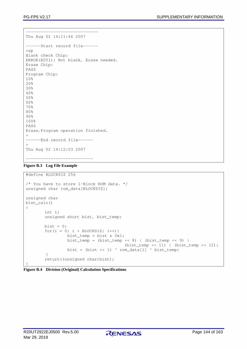
PG-FP5 V2.17 SUPPLEMENTARY INFORMATION
R20UT2922EJ0500 Rev.5.00 Page 144 of 163 Mar 29, 2019
----------------------------- Thu Aug 02 14:11:46 2007 ------Start record file------ >ep Blank check Chip: ERROR(E051): Not blank, Erase needed. Erase Chip: PASS Program Chip: 10% 20% 30% 40% 50% 60% 70% 80% 90% 100% PASS Erase,Program operation finished. > ------End record file------ > Thu Aug 02 14:12:03 2007 ---------------------------
Figure B.3 Log File Example
#define BLOCKSIZ 256 /* You have to store 1-Block ROM data. */ unsigned char rom_data[BLOCKSIZ]; unsigned char bist_calc()
int i; unsigned short bist, bist_temp;
bist = 0; for(i = 0; i < BLOCKSIZ; i++)
bist_temp = bist & 0x1; bist_temp = (bist_temp << 8) | (bist_temp << 9) |
(bist_temp << 11) | (bist_temp << 12); bist = (bist >> 1) ^ rom_data[i] ^ bist_temp;
return((unsigned char)bist);
Figure B.4 Division (Original) Calculation Specifications
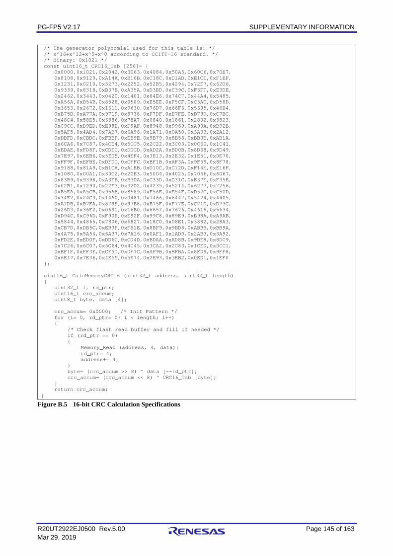
PG-FP5 V2.17 SUPPLEMENTARY INFORMATION
R20UT2922EJ0500 Rev.5.00 Page 145 of 163 Mar 29, 2019
/* The generator polynomial used for this table is: */ /* x^16+x^12+x^5+x^0 according to CCITT-16 standard. */ /* Binary: 0x1021 */ const uint16_t CRC16_Tab [256]= 0x0000,0x1021,0x2042,0x3063,0x4084,0x50A5,0x60C6,0x70E7, 0x8108,0x9129,0xA14A,0xB16B,0xC18C,0xD1AD,0xE1CE,0xF1EF, 0x1231,0x0210,0x3273,0x2252,0x52B5,0x4294,0x72F7,0x62D6, 0x9339,0x8318,0xB37B,0xA35A,0xD3BD,0xC39C,0xF3FF,0xE3DE, 0x2462,0x3443,0x0420,0x1401,0x64E6,0x74C7,0x44A4,0x5485, 0xA56A,0xB54B,0x8528,0x9509,0xE5EE,0xF5CF,0xC5AC,0xD58D, 0x3653,0x2672,0x1611,0x0630,0x76D7,0x66F6,0x5695,0x46B4, 0xB75B,0xA77A,0x9719,0x8738,0xF7DF,0xE7FE,0xD79D,0xC7BC, 0x48C4,0x58E5,0x6886,0x78A7,0x0840,0x1861,0x2802,0x3823, 0xC9CC,0xD9ED,0xE98E,0xF9AF,0x8948,0x9969,0xA90A,0xB92B, 0x5AF5,0x4AD4,0x7AB7,0x6A96,0x1A71,0x0A50,0x3A33,0x2A12, 0xDBFD,0xCBDC,0xFBBF,0xEB9E,0x9B79,0x8B58,0xBB3B,0xAB1A, 0x6CA6,0x7C87,0x4CE4,0x5CC5,0x2C22,0x3C03,0x0C60,0x1C41, 0xEDAE,0xFD8F,0xCDEC,0xDDCD,0xAD2A,0xBD0B,0x8D68,0x9D49, 0x7E97,0x6EB6,0x5ED5,0x4EF4,0x3E13,0x2E32,0x1E51,0x0E70, 0xFF9F,0xEFBE,0xDFDD,0xCFFC,0xBF1B,0xAF3A,0x9F59,0x8F78, 0x9188,0x81A9,0xB1CA,0xA1EB,0xD10C,0xC12D,0xF14E,0xE16F, 0x1080,0x00A1,0x30C2,0x20E3,0x5004,0x4025,0x7046,0x6067, 0x83B9,0x9398,0xA3FB,0xB3DA,0xC33D,0xD31C,0xE37F,0xF35E, 0x02B1,0x1290,0x22F3,0x32D2,0x4235,0x5214,0x6277,0x7256, 0xB5EA,0xA5CB,0x95A8,0x8589,0xF56E,0xE54F,0xD52C,0xC50D, 0x34E2,0x24C3,0x14A0,0x0481,0x7466,0x6447,0x5424,0x4405, 0xA7DB,0xB7FA,0x8799,0x97B8,0xE75F,0xF77E,0xC71D,0xD73C, 0x26D3,0x36F2,0x0691,0x16B0,0x6657,0x7676,0x4615,0x5634, 0xD94C,0xC96D,0xF90E,0xE92F,0x99C8,0x89E9,0xB98A,0xA9AB, 0x5844,0x4865,0x7806,0x6827,0x18C0,0x08E1,0x3882,0x28A3, 0xCB7D,0xDB5C,0xEB3F,0xFB1E,0x8BF9,0x9BD8,0xABBB,0xBB9A, 0x4A75,0x5A54,0x6A37,0x7A16,0x0AF1,0x1AD0,0x2AB3,0x3A92, 0xFD2E,0xED0F,0xDD6C,0xCD4D,0xBDAA,0xAD8B,0x9DE8,0x8DC9, 0x7C26,0x6C07,0x5C64,0x4C45,0x3CA2,0x2C83,0x1CE0,0x0CC1, 0xEF1F,0xFF3E,0xCF5D,0xDF7C,0xAF9B,0xBFBA,0x8FD9,0x9FF8, 0x6E17,0x7E36,0x4E55,0x5E74,0x2E93,0x3EB2,0x0ED1,0x1EF0 ; uint16_t CalcMemoryCRC16 (uint32_t address, uint32_t length) uint32_t i, rd_ptr; uint16_t crc_accum; uint8_t byte, data [4]; crc_accum= 0x0000; /* Init Pattern */ for (i= 0, rd_ptr= 0; i < length; i++) /* Check flash read buffer and fill if needed */ if (rd_ptr == 0) Memory_Read (address, 4, data); rd_ptr= 4; address+= 4; byte= (crc_accum >> 8) ^ data [--rd_ptr]; crc_accum= (crc_accum << 8) ^ CRC16_Tab [byte]; return crc_accum;
Figure B.5 16-bit CRC Calculation Specifications
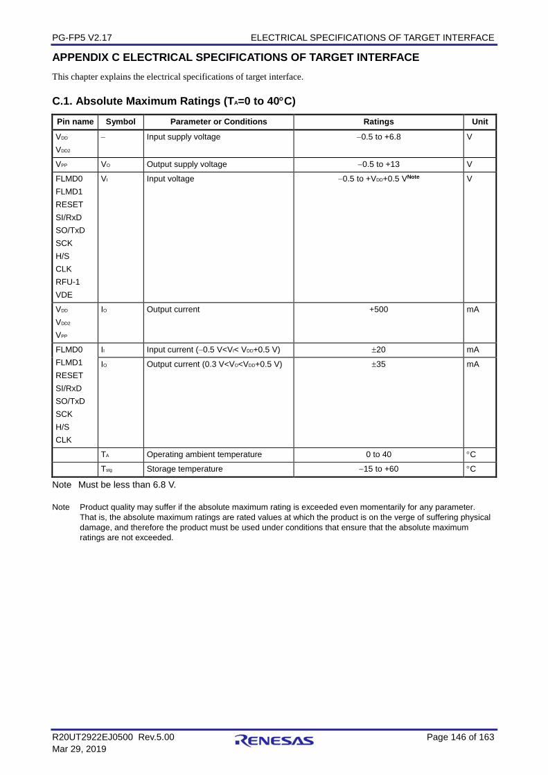
PG-FP5 V2.17 ELECTRICAL SPECIFICATIONS OF TARGET INTERFACE
R20UT2922EJ0500 Rev.5.00 Page 146 of 163 Mar 29, 2019
APPENDIX C ELECTRICAL SPECIFICATIONS OF TARGET INTERFACE This chapter explains the electrical specifications of target interface. C.1. Absolute Maximum Ratings (TA=0 to 40°C)
Pin name Symbol Parameter or Conditions Ratings Unit
VDD VDD2
− Input supply voltage −0.5 to +6.8 V
VPP VO Output supply voltage −0.5 to +13 V
FLMD0 FLMD1 RESET SI/RxD SO/TxD SCK H/S CLK RFU-1 VDE
VI Input voltage −0.5 to +VDD+0.5 VNote V
VDD VDD2 VPP
IO Output current +500 mA
FLMD0 FLMD1 RESET SI/RxD SO/TxD SCK H/S CLK
II Input current (−0.5 V<VI< VDD+0.5 V) ±20 mA
IO Output current (0.3 V<VO<VDD+0.5 V) ±35 mA
TA Operating ambient temperature 0 to 40 °C
Tstg Storage temperature −15 to +60 °C
Note Must be less than 6.8 V. Note Product quality may suffer if the absolute maximum rating is exceeded even momentarily for any parameter.
That is, the absolute maximum ratings are rated values at which the product is on the verge of suffering physical damage, and therefore the product must be used under conditions that ensure that the absolute maximum ratings are not exceeded.
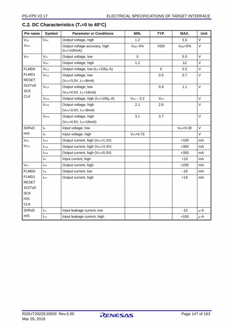
PG-FP5 V2.17 ELECTRICAL SPECIFICATIONS OF TARGET INTERFACE
R20UT2922EJ0500 Rev.5.00 Page 147 of 163 Mar 29, 2019
C.2. DC Characteristics (TA=0 to 40°C) Pin name Symbol Parameter or Conditions MIN. TYP. MAX. Unit
VDD VDD2
VOH Output voltage, high 1.2 5.5 V
Output voltage accuracy, high (IOH=100mA)
VDD−5% VDD VDD+5% V
VPP VOL Output voltage, low 0 5.5 V
VOH Output voltage, high 1.2 12 V
FLMD0 FLMD1 RESET SO/TxD SCK CLK
VOL1 Output voltage, low (IOL=100µ A) 0 0.2 V
VOL2 Output voltage, low (VDD=3.0V, IOL=8mA)
0.5 0.7 V
VOL3 Output voltage, low (VDD=4.5V, IOL=16mA)
0.9 1.1 V
VOH1 Output voltage, high (IOH=100µ A) VDD – 0.2 VDD V
VOH2 Output voltage, high (VDD=3.0V, IOH=8mA)
2.1 2.6 V
VOH3 Output voltage, high (VDD=4.5V, IOH=16mA)
3.1 3.7 V
SI/RxD H/S
IIL Input voltage, low VDD×0.30 V
IIH Input voltage, high VDD×0.75 V
VDD VDD2
IOH1 Output current, high (VDD=1.2V) +100 mA
IOH2 Output current, high (VDD=3.3V) +300 mA
IOH3 Output current, high (VDD=5.0V) +350 mA
IIH Input current, high +10 mA
VPP IOH Output current, high +200 mA
FLMD0 FLMD1 RESET SO/TxD SCK H/S CLK
IOL Output current, low −16 mA
IOH Output current, high +16 mA
SI/RxD H/S
ILIL Input leakage current, low −10 µ A
ILIH Input leakage current, high +100 µ A
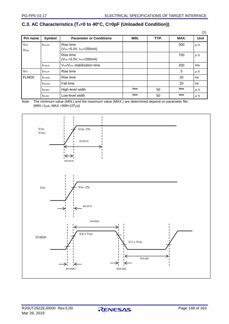
PG-FP5 V2.17 ELECTRICAL SPECIFICATIONS OF TARGET INTERFACE
R20UT2922EJ0500 Rev.5.00 Page 148 of 163 Mar 29, 2019
C.3. AC Characteristics (TA=0 to 40°C, C=0pF (Unloaded Condition)) (1)
Pin name Symbol Parameter or Conditions MIN. TYP. MAX. Unit
VDD VDD2
tPLHVD Rise time (VDD =5.0V, IOH=200mA)
300 µ s
Rise time (VDD =3.3V, IOH=200mA)
700 µ s
tSTBVD VDD/VDD2 stabilization time 200 ms
VPP tPHLVP Rise time 5 µ s
FLMD0 tPLHMD Rise time 20 ns
tPHLMD Fall time 20 ns
tWHMD High-level width Note 50 Note µ s
tWLMD Low-level width Note 50 Note µ s
Note The minimum value (MIN.) and the maximum value (MAX.) are determined depend on parameter file. (MIN.=1µs, MAX.=999×109µs)
tPLHVD
VDD VDD2
VPP
FLMD0
tPLHMD tPHLMD
tPLHVP
tSTBVD
tWHMD
tWLMD
0.8 x VDD
0.2 x VDD
VPP−5%
VDD−5%
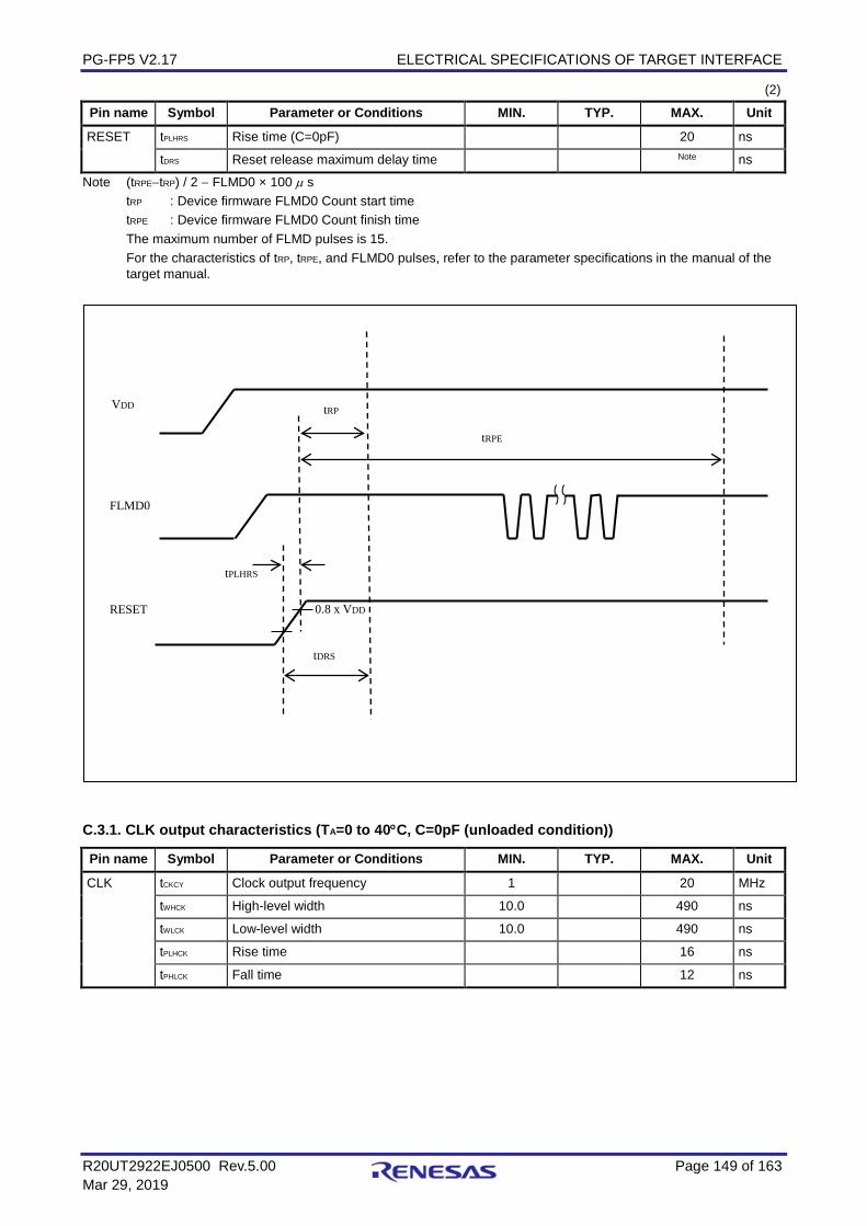
PG-FP5 V2.17 ELECTRICAL SPECIFICATIONS OF TARGET INTERFACE
R20UT2922EJ0500 Rev.5.00 Page 149 of 163 Mar 29, 2019
(2)
Pin name Symbol Parameter or Conditions MIN. TYP. MAX. Unit
RESET tPLHRS Rise time (C=0pF) 20 ns
tDRS Reset release maximum delay time Note ns
Note (tRPE−tRP) / 2 − FLMD0 × 100 µ s tRP : Device firmware FLMD0 Count start time tRPE : Device firmware FLMD0 Count finish time The maximum number of FLMD pulses is 15. For the characteristics of tRP, tRPE, and FLMD0 pulses, refer to the parameter specifications in the manual of the
target manual.
C.3.1. CLK output characteristics (TA=0 to 40°C, C=0pF (unloaded condition))
Pin name Symbol Parameter or Conditions MIN. TYP. MAX. Unit
CLK tCKCY Clock output frequency 1 20 MHz
tWHCK High-level width 10.0 490 ns
tWLCK Low-level width 10.0 490 ns
tPLHCK Rise time 16 ns
tPHLCK Fall time 12 ns
tDRS
RESET
VDD
FLMD0
tRP
tRPE
tPLHRS
0.8 x VDD
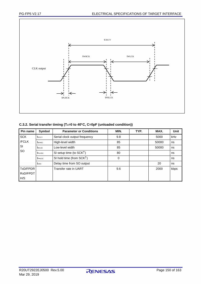
PG-FP5 V2.17 ELECTRICAL SPECIFICATIONS OF TARGET INTERFACE
R20UT2922EJ0500 Rev.5.00 Page 150 of 163 Mar 29, 2019
C.3.2. Serial transfer timing (TA=0 to 40°C, C=0pF (unloaded condition))
Pin name Symbol Parameter or Conditions MIN. TYP. MAX. Unit
SCK /FCLK SI SO
tSCCY Serial clock output frequency 9.8 5000 kHz
tWHSC High-level width 85 50000 ns
tWLSC Low-level width 85 50000 ns
tPLHSC SI setup time (to SCK↑) 80 ns
tPHLSC SI hold time (from SCK↑) 0 ns
tDSC Delay time from SO output 20 ns
TxD/FPDR RxD/FPDT H/S
Transfer rate in UART 9.6 2000 kbps
tCKCY
tWLCK tWHCK
tPLHCK tPHLCK
CLK output
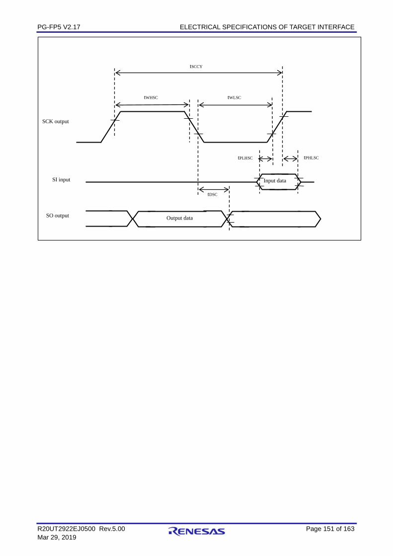
PG-FP5 V2.17 ELECTRICAL SPECIFICATIONS OF TARGET INTERFACE
R20UT2922EJ0500 Rev.5.00 Page 151 of 163 Mar 29, 2019
tSCCY
tWLSC tWHSC
tPLHSC tPHLSC
SCK output
SI input
SO output
Input data
Output data
tDSC
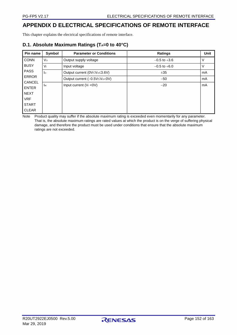
PG-FP5 V2.17 ELECTRICAL SPECIFICATIONS OF REMOTE INTERFACE
R20UT2922EJ0500 Rev.5.00 Page 152 of 163 Mar 29, 2019
APPENDIX D ELECTRICAL SPECIFICATIONS OF REMOTE INTERFACE This chapter explains the electrical specifications of remote interface. D.1. Absolute Maximum Ratings (TA=0 to 40°C)
Pin name Symbol Parameter or Conditions Ratings Unit
CONN BUSY PASS ERROR CANCEL ENTER NEXT VRF START CLEAR
VO Output supply voltage −0.5 to +3.6 V
VI Input voltage −0.5 to +6.0 V
IO Output current (0V≤VO≤3.6V) ±35 mA
Output current (−0.5V≤VO<0V) −50 mA
IIK Input current (VI <0V) −20 mA
Note Product quality may suffer if the absolute maximum rating is exceeded even momentarily for any parameter. That is, the absolute maximum ratings are rated values at which the product is on the verge of suffering physical damage, and therefore the product must be used under conditions that ensure that the absolute maximum ratings are not exceeded.
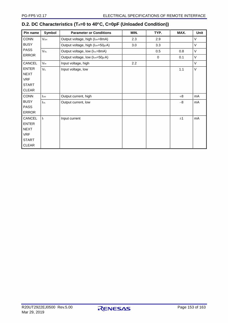
PG-FP5 V2.17 ELECTRICAL SPECIFICATIONS OF REMOTE INTERFACE
R20UT2922EJ0500 Rev.5.00 Page 153 of 163 Mar 29, 2019
D.2. DC Characteristics (TA=0 to 40°C, C=0pF (Unloaded Condition)) Pin name Symbol Parameter or Conditions MIN. TYP. MAX. Unit
CONN BUSY PASS ERROR
VOH Output voltage, high (IOH=8mA) 2.3 2.9 V
Output voltage, high (IOH=50µA) 3.0 3.3 V
VOL Output voltage, low (IOL=8mA) 0.5 0.8 V
Output voltage, low (IOH=50µA) 0 0.1 V
CANCEL ENTER NEXT VRF START CLEAR
VIH Input voltage, high 2.2 V
VIL Input voltage, low 1.1 V
CONN BUSY PASS ERROR
IOH Output current, high +8 mA
IOL Output current, low −8 mA
CANCEL ENTER NEXT VRF START CLEAR
II Input current ±1 mA
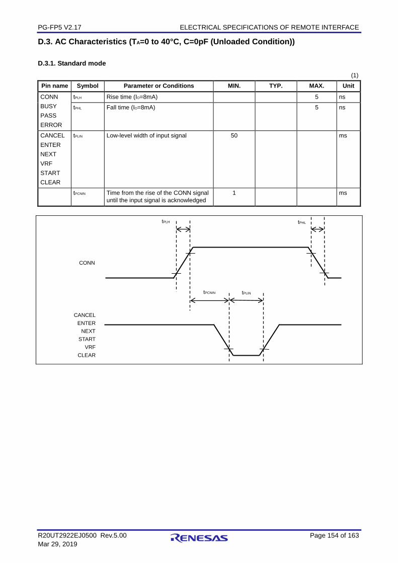
PG-FP5 V2.17 ELECTRICAL SPECIFICATIONS OF REMOTE INTERFACE
R20UT2922EJ0500 Rev.5.00 Page 154 of 163 Mar 29, 2019
D.3. AC Characteristics (TA=0 to 40°C, C=0pF (Unloaded Condition)) D.3.1. Standard mode
(1)
Pin name Symbol Parameter or Conditions MIN. TYP. MAX. Unit
CONN BUSY PASS ERROR
tPLH Rise time (IO=8mA) 5 ns
tPHL Fall time (IO=8mA) 5 ns
CANCEL ENTER NEXT VRF START CLEAR
tPLIN Low-level width of input signal 50 ms
tPCNIN Time from the rise of the CONN signal until the input signal is acknowledged
1 ms
CONN
tPLIN
tPHL tPLH
tPCNIN
CANCEL ENTER
NEXT START
VRF CLEAR
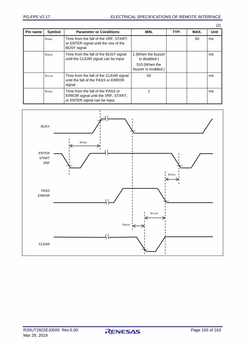
PG-FP5 V2.17 ELECTRICAL SPECIFICATIONS OF REMOTE INTERFACE
R20UT2922EJ0500 Rev.5.00 Page 155 of 163 Mar 29, 2019
(2)
Pin name Symbol Parameter or Conditions MIN. TYP. MAX. Unit
tPINBU Time from the fall of the VRF, START, or ENTER signal until the rise of the BUSY signal
50 ms
tPBUIN Time from the fall of the BUSY signal until the CLEAR signal can be input
1 (When the buzzer is disabled.)
510 (When the buzzer is enabled.)
ms
tPCLPE Time from the fall of the CLEAR signal until the fall of the PASS or ERROR signal
50 ms
tPPEIN Time from the fall of the PASS or ERROR signal until the VRF, START, or ENTER signal can be input
1 ms
BUSY
tPBUIN
tPCLPE
tPINBU
PASS ERROR
ENTER START
VRF
tPPEIN
CLEAR

PG-FP5 V2.17 ELECTRICAL SPECIFICATIONS OF REMOTE INTERFACE
R20UT2922EJ0500 Rev.5.00 Page 156 of 163 Mar 29, 2019
D.3.2. Bank mode (1)
Pin name Symbol Parameter or Conditions MIN. TYP. MAX. Unit
CONN BUSY PASS ERROR
tPLH Rise time (IO=8mA) 5 ns
tPHL Fall time (IO=8mA) 5 ns
BANK0 BANK1 BANK2 VRF START CLEAR
tPLIN Low-level width of input signal 50 ms
tPCNIN Time from the rise of the CONN signal until the input signal is acknowledged
1 ms
CONN
tPLIN
tPHL tPLH
tPCNIN
BANK0 BANK1 BANK2 START
VRF CLEAR
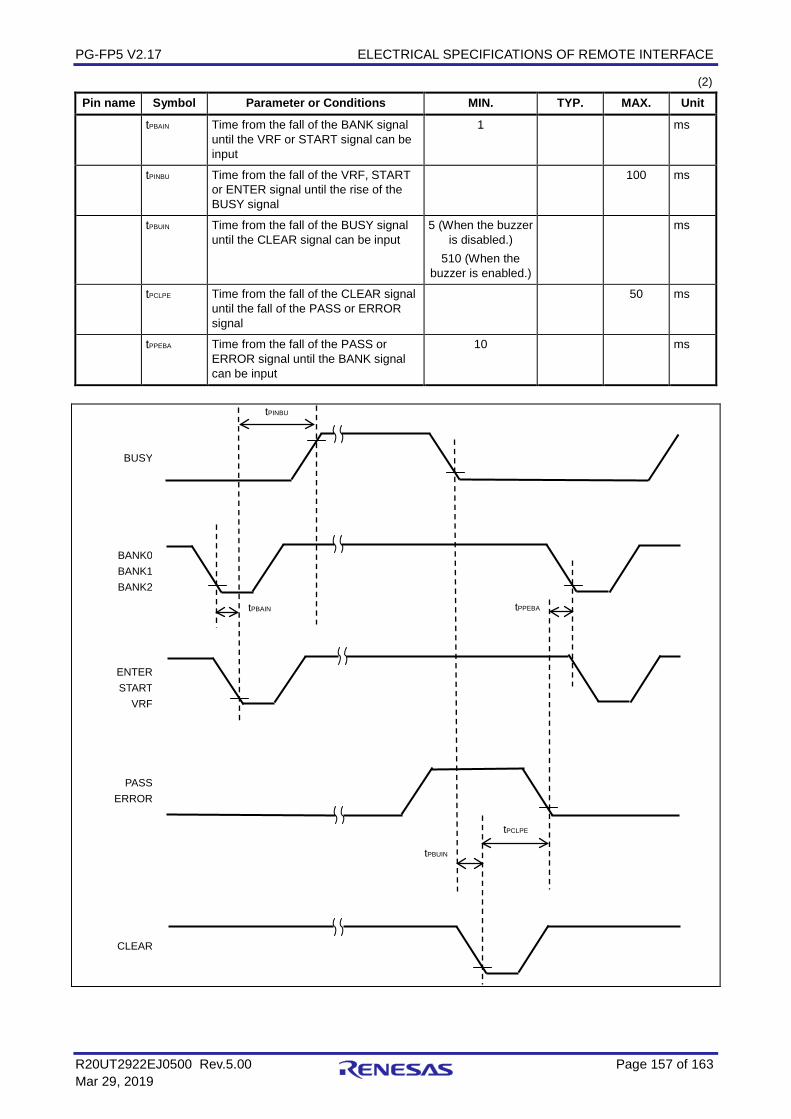
PG-FP5 V2.17 ELECTRICAL SPECIFICATIONS OF REMOTE INTERFACE
R20UT2922EJ0500 Rev.5.00 Page 157 of 163 Mar 29, 2019
(2)
Pin name Symbol Parameter or Conditions MIN. TYP. MAX. Unit
tPBAIN Time from the fall of the BANK signal until the VRF or START signal can be input
1 ms
tPINBU Time from the fall of the VRF, START or ENTER signal until the rise of the BUSY signal
100 ms
tPBUIN Time from the fall of the BUSY signal until the CLEAR signal can be input
5 (When the buzzer is disabled.)
510 (When the buzzer is enabled.)
ms
tPCLPE Time from the fall of the CLEAR signal until the fall of the PASS or ERROR signal
50 ms
tPPEBA Time from the fall of the PASS or ERROR signal until the BANK signal can be input
10 ms
BUSY
tPINBU
tPBAIN
BANK0 BANK1 BANK2
tPPEBA
ENTERSTART
VRF
tPBUIN
tPCLPE
PASS ERROR
CLEAR
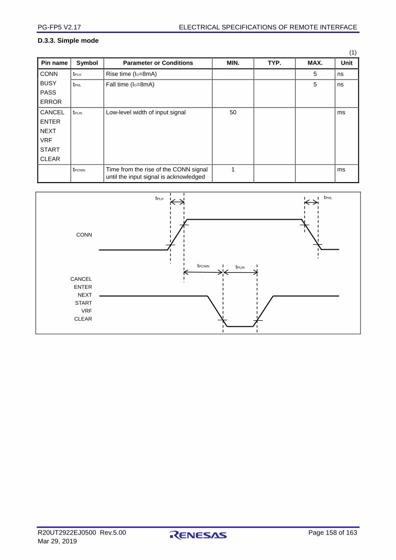
PG-FP5 V2.17 ELECTRICAL SPECIFICATIONS OF REMOTE INTERFACE
R20UT2922EJ0500 Rev.5.00 Page 158 of 163 Mar 29, 2019
D.3.3. Simple mode (1)
Pin name Symbol Parameter or Conditions MIN. TYP. MAX. Unit
CONN BUSY PASS ERROR
tPLH Rise time (IO=8mA) 5 ns
tPHL Fall time (IO=8mA) 5 ns
CANCEL ENTER NEXT VRF START CLEAR
tPLIN Low-level width of input signal 50 ms
tPCNIN Time from the rise of the CONN signal until the input signal is acknowledged
1 ms
CONN
tPLIN
tPHL tPLH
tPCNIN
CANCEL ENTER
NEXT START
VRF CLEAR
PG-FP5 V2.17 ELECTRICAL SPECIFICATIONS OF REMOTE INTERFACE
R20UT2922EJ0500 Rev.5.00 Page 159 of 163 Mar 29, 2019
(2)
Pin name Symbol Parameter or Conditions MIN. TYP. MAX. Unit
tPBAIN Time from the fall of the NEXT signal until the VRF or START signal can be input
1 ms
tPINBU Time from the fall of the VRF, START or ENTER signal until the rise of the BUSY signal (When the input signal is input after having changed the program area)
8 s
Time from the fall of the VRF, START or ENTER signal until the rise of the BUSY signal (When the input signal is input without changing the program area)
50 ms
tPBUIN Time from the fall of the BUSY signal until the CLEAR signal can be input
1 (When the buzzer is disabled.)
510 (When the buzzer is enabled.)
ms
tPCLPE Time from the fall of the CLEAR signal until the fall of the PASS or ERROR signal
50 ms
tPPENE Time from the fall of the PASS or ERROR signal until the NEXT signal can be input
1 ms
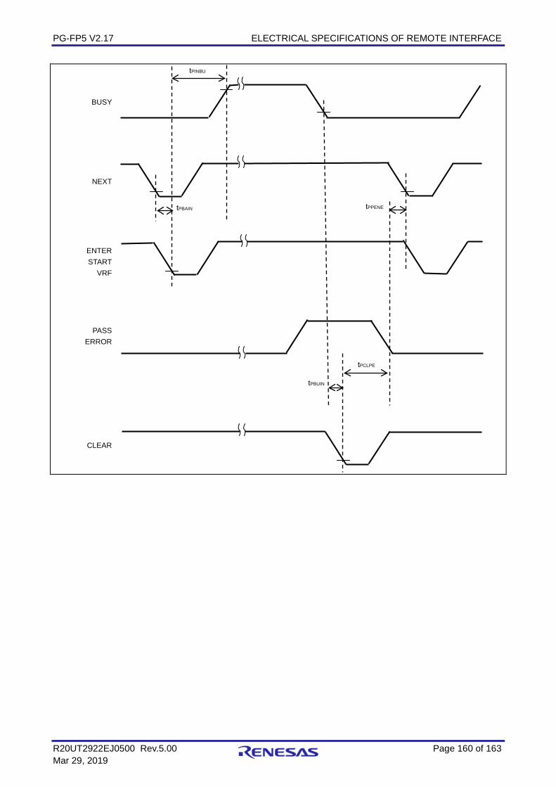
PG-FP5 V2.17 ELECTRICAL SPECIFICATIONS OF REMOTE INTERFACE
R20UT2922EJ0500 Rev.5.00 Page 160 of 163 Mar 29, 2019
BUSY
tPINBU
tPBAIN
NEXT
tPPENE
ENTER START
VRF
tPBUIN
tPCLPE
PASS ERROR
CLEAR

Colophon
PG-FP5 V2.17 User’s Manual Common Publication Date: Rev.5.00 Mar 29, 2019 Published by: Renesas Electronics Corporation
© 2019 Renesas Electronics Corporation. All rights reserved.Colophon 5.2
http://www.renesas.comRefer to "http://www.renesas.com/" for the latest and detailed information.
Renesas Electronics CorporationTOYOSU FORESIA, 3-2-24 Toyosu, Koto-ku, Tokyo 135-0061, JapanRenesas Electronics America Inc.1001 Murphy Ranch Road, Milpitas, CA 95035, U.S.A.Tel: +1-408-432-8888, Fax: +1-408-434-5351Renesas Electronics Canada Limited9251 Yonge Street, Suite 8309 Richmond Hill, Ontario Canada L4C 9T3Tel: +1-905-237-2004Renesas Electronics Europe LimitedDukes Meadow, Millboard Road, Bourne End, Buckinghamshire, SL8 5FH, U.KTel: +44-1628-651-700Renesas Electronics Europe GmbHArcadiastrasse 10, 40472 Düsseldorf, Germany Tel: +49-211-6503-0, Fax: +49-211-6503-1327Renesas Electronics (China) Co., Ltd.Room 1709 Quantum Plaza, No.27 ZhichunLu, Haidian District, Beijing, 100191 P. R. ChinaTel: +86-10-8235-1155, Fax: +86-10-8235-7679Renesas Electronics (Shanghai) Co., Ltd.Unit 301, Tower A, Central Towers, 555 Langao Road, Putuo District, Shanghai, 200333 P. R. China Tel: +86-21-2226-0888, Fax: +86-21-2226-0999Renesas Electronics Hong Kong LimitedUnit 1601-1611, 16/F., Tower 2, Grand Century Place, 193 Prince Edward Road West, Mongkok, Kowloon, Hong KongTel: +852-2265-6688, Fax: +852 2886-9022Renesas Electronics Taiwan Co., Ltd.13F, No. 363, Fu Shing North Road, Taipei 10543, TaiwanTel: +886-2-8175-9600, Fax: +886 2-8175-9670Renesas Electronics Singapore Pte. Ltd.80 Bendemeer Road, Unit #06-02 Hyflux Innovation Centre, Singapore 339949Tel: +65-6213-0200, Fax: +65-6213-0300Renesas Electronics Malaysia Sdn.Bhd.Unit 1207, Block B, Menara Amcorp, Amcorp Trade Centre, No. 18, Jln Persiaran Barat, 46050 Petaling Jaya, Selangor Darul Ehsan, MalaysiaTel: +60-3-7955-9390, Fax: +60-3-7955-9510Renesas Electronics India Pvt. Ltd.No.777C, 100 Feet Road, HAL 2nd Stage, Indiranagar, Bangalore 560 038, IndiaTel: +91-80-67208700, Fax: +91-80-67208777Renesas Electronics Korea Co., Ltd.17F, KAMCO Yangjae Tower, 262, Gangnam-daero, Gangnam-gu, Seoul, 06265 KoreaTel: +82-2-558-3737, Fax: +82-2-558-5338
SALES OFFICES

Backcover
R20UT2922EJ0500
PG-FP5 V2.17