Embed Size (px)
Citation preview

PSI5 Technical Specification Base Standard V2.3 01/2018
All r
igh
ts in
clu
din
g in
dustr
ial p
rop
ert
y r
igh
ts a
nd
all r
igh
ts o
f d
isp
osal such
as c
opyin
g a
nd
passin
g t
o t
hir
d p
art
ies
rese
rve
d.
Peripheral Sensor Interface – Base Standard
PSI5 Technical
Specification
V2.3
Peripheral Sensor Interface
for Automotive Applications

PSI5 Technical Specification Base Standard V2.3 01/2018
All r
igh
ts in
clu
din
g in
dustr
ial p
rop
ert
y r
igh
ts a
nd
all r
igh
ts o
f d
isp
osal such
as c
opyin
g a
nd
passin
g t
o t
hir
d p
art
ies
rese
rve
d.
Peripheral Sensor Interface – Base Standard
PSI5 Technical
Specification
I
V2.3
Contents
1 Introduction 1
1.1 Description .................................................................................................................................. 1
1.2 PSI5 Main Features .................................................................................................................... 1
1.3 Scope ......................................................................................................................................... 2
1.4 Legal Information ........................................................................................................................ 2
1.4.1 Disclaimer ......................................................................................................................... 2
1.4.2 Indemnification .................................................................................................................. 2
2 Definition of Terms 4
2.1 Glossary ..................................................................................................................................... 4
2.2 Symbols / Parameters ................................................................................................................. 5
2.2.1 General Parameters .......................................................................................................... 5
2.2.2 Communication Parameters .............................................................................................. 6
2.2.3 Supply Line and Bus Parameters....................................................................................... 7
2.3 Acronyms, Abbreviations ............................................................................................................. 8
3 Data Link Layer 9
3.1 Sensor to ECU Communication ................................................................................................... 9
3.1.1 Data Frames ..................................................................................................................... 9
3.1.2 Data Frame Format ........................................................................................................... 9
3.1.3 Scaling of Sensor Output (for data words longer than 10 bit) ............................................ 10
3.1.4 Serial Channel................................................................................................................. 11
3.2 ECU to Sensor Communication ................................................................................................. 12
3.2.1 Data Frames ................................................................................................................... 12
3.2.2 Frame Formats - Tooth Gap method................................................................................ 12
3.2.3 Frame Formats – Pulse Width method ............................................................................. 13
3.2.4 Mapping of Data frames for Pulse Width method ............................................................. 14
3.3 Error Detection .......................................................................................................................... 15
3.3.1 Parity Bit ......................................................................................................................... 15
3.3.2 3 bit CRC ........................................................................................................................ 15
3.3.3 6 bit CRC ........................................................................................................................ 16
4 Physical Layer 18
4.1 General ..................................................................................................................................... 18
4.2 Supply Line Model..................................................................................................................... 18
4.3 Single Sensor, Point to Point Topologies ................................................................................... 19
4.3.1 Single Sensor, Point to Point Asynchronous Topologies (PSI5-A) .................................... 19
4.3.2 Parameter Specification for Single Sensor Configuration ................................................. 19
4.4 Multi Sensor, Bus Topologies .................................................................................................... 19

PSI5 Technical Specification Base Standard V2.3 01/2018
All r
igh
ts in
clu
din
g in
dustr
ial p
rop
ert
y r
igh
ts a
nd
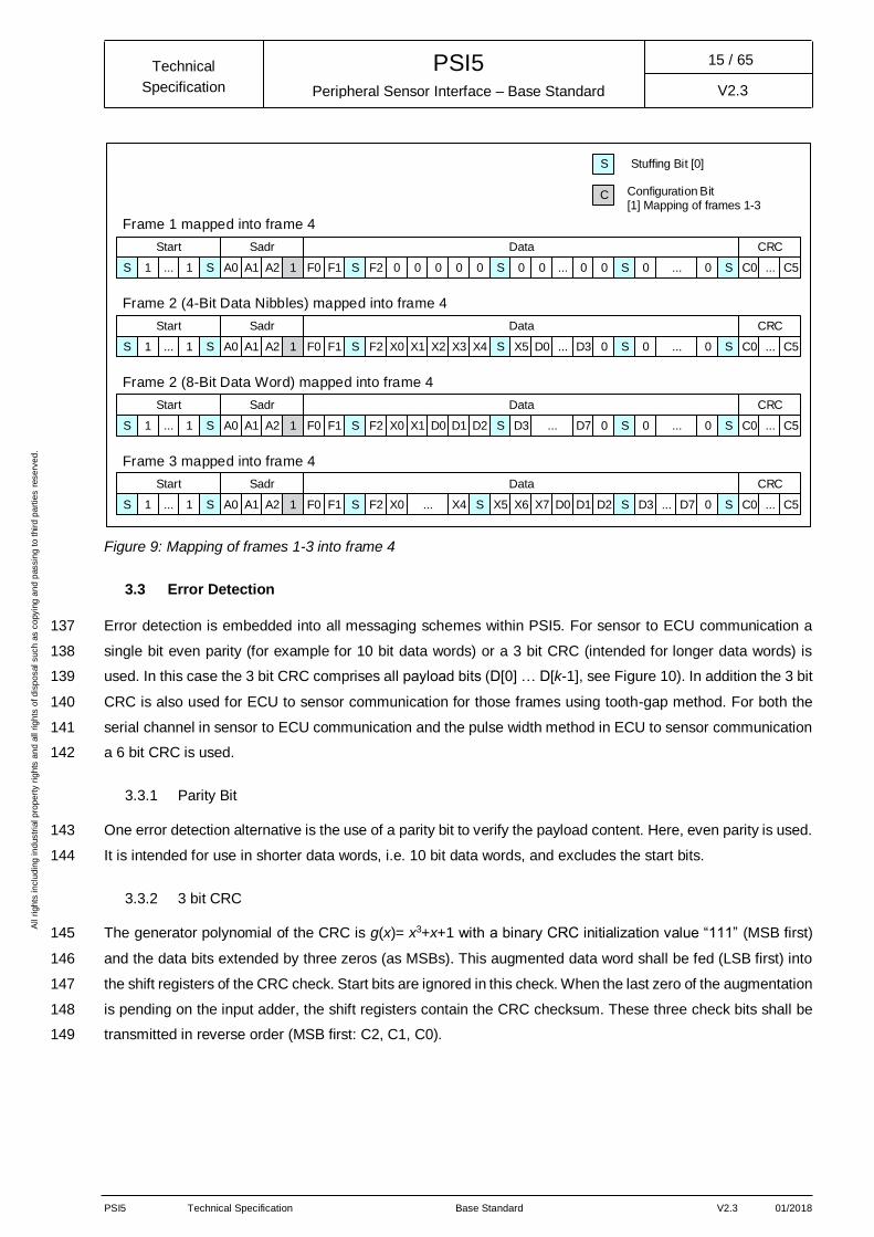
all r
igh
ts o
f d
isp
osal such
as c
opyin
g a
nd
passin
g t
o t
hir
d p
art
ies
rese
rve
d.
Peripheral Sensor Interface – Base Standard
PSI5 Technical
Specification
II
V2.3
4.4.1 Synchronous Parallel Bus Mode (PSI5-P) ........................................................................ 19
4.4.2 Synchronous Universal Bus Mode (PSI5-U)..................................................................... 20
4.4.3 Synchronous Daisy Chain Bus Mode (PSI5-D) ................................................................ 21
4.4.4 Parameter Specification for Bus Topologies..................................................................... 22
4.5 Sensor to ECU Communication ................................................................................................. 23
4.6 ECU to Sensor Communication ................................................................................................. 24
4.6.1 Tooth Gap method .......................................................................................................... 24
4.6.2 Pulse Width method ........................................................................................................ 24
4.7 General Parameters .................................................................................................................. 25
4.7.1 Supply and Communication Parameters Definitions ......................................................... 25
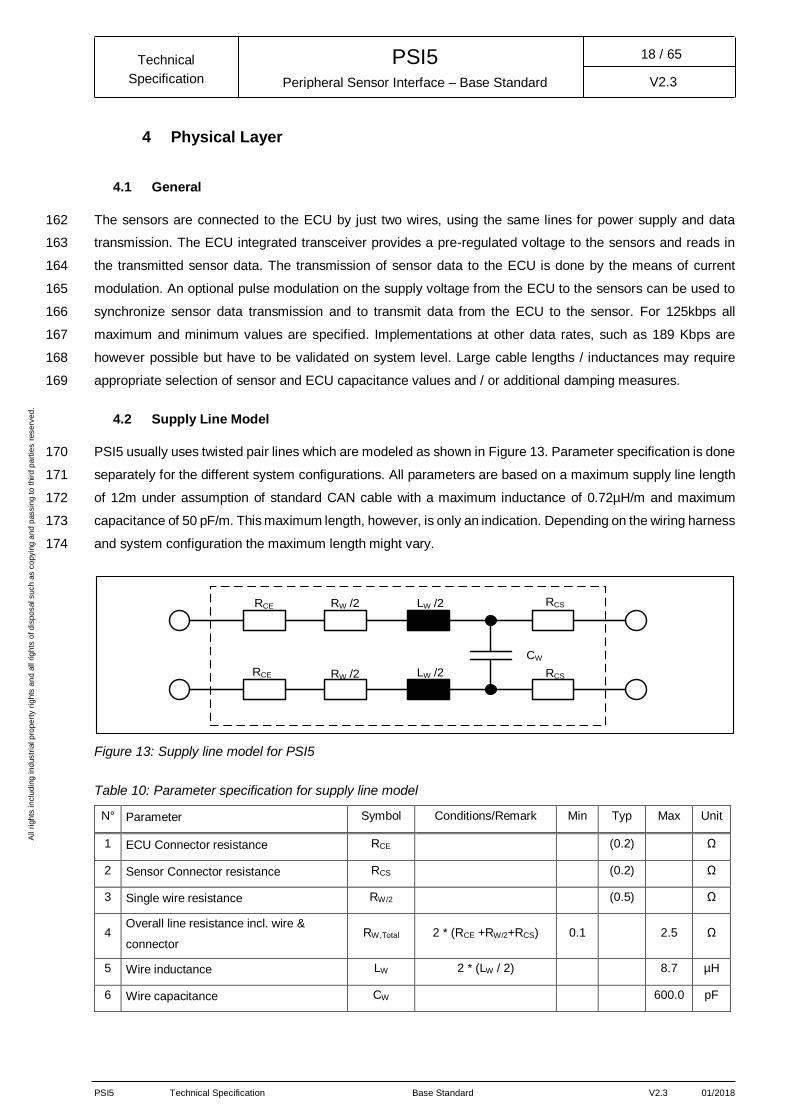
4.7.2 Absolute Maximum Ratings ............................................................................................. 28
4.7.3 Configuration Modes & Options ....................................................................................... 28
4.8 Dynamic Bus Behavior .............................................................................................................. 30
4.8.1 Test Network Parameters ................................................................................................ 30
4.8.1.1 Sensor Damping Behavior ................................................................................ 30
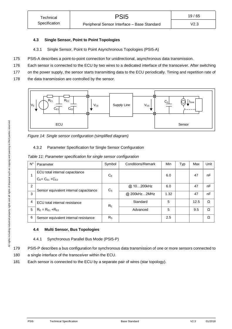
4.8.1.2 Sensor Testing ................................................................................................. 31
4.8.1.3 ECU Testing ..................................................................................................... 32
4.8.2 Requirements for Dynamic Sensor Testing ...................................................................... 32
4.8.3 Requirements for Dynamic ECU Testing.......................................................................... 33
4.9 Synchronization Signal .............................................................................................................. 34
4.10 Timing Definitions for Synchronous Operation Modes ................................................................ 38
4.10.1 Generic Time Slot Calculation ......................................................................................... 39
4.11 Sensor Power-on Characteristics .............................................................................................. 41
4.11.1 Sensor Bus Configuration ................................................................................................ 41
4.11.2 Extended Settling Time for Single Sensor Configuration .................................................. 42
4.12 Undervoltage Reset and Microcut Rejection .............................................................................. 43
5 Application Layer 45
5.1 Data Range ............................................................................................................................... 45
5.1.1 Scaling of Sensor Output ................................................................................................. 46
5.2 Sensor Initialization / Identification ............................................................................................. 46
5.2.1 Frame Format - Data Range Initialization ......................................................................... 47
5.2.2 Data Content - Data Range Initialization .......................................................................... 48
5.2.3 Meta Information ............................................................................................................. 49
5.2.4 Vendor ID ........................................................................................................................ 50
5.3 Bidirectional Communication ..................................................................................................... 51
5.3.1 Sensor Addresses ........................................................................................................... 51
5.3.2 Function Codes and Responses for Bidirectional Communication – Frame 1 to 3 ............ 52
5.3.3 Returned Error Codes – Sensor Response for Frame 1-3 ................................................ 52
6 System Setup & Operation Modes 54
PSI5 Technical Specification Base Standard V2.3 01/2018
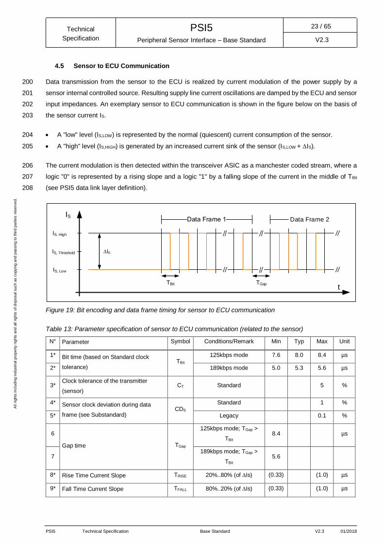
All r
igh
ts in
clu
din
g in
dustr
ial p
rop
ert
y r
igh
ts a
nd
all r
igh
ts o
f d
isp
osal such
as c
opyin
g a
nd
passin
g t
o t
hir
d p
art
ies
rese
rve
d.
Peripheral Sensor Interface – Base Standard
PSI5 Technical
Specification
III
V2.3
6.1 System Setup............................................................................................................................ 54
6.2 PSI5 Operation Modes .............................................................................................................. 54
6.3 Asynchronous Operation (PSI5-A) ............................................................................................. 56
6.4 Synchronous Operation ............................................................................................................. 56
6.4.1 Timing of Synchronous Operation Modes ........................................................................ 57
6.4.2 Bus Operation Principle ................................................................................................... 57
6.4.2.1 Preferred Daisy-Chain Mode: Parallel Initialization Phase) ................................ 58
6.4.3 Sensor Cluster / Multichannel .......................................................................................... 59
7 Interoperability Requirements 61
8 Document History & Modifications 62

PSI5 Technical Specification Base Standard V2.3 01/2018
All r
igh
ts in
clu
din
g in
dustr
ial p
rop
ert
y r
igh
ts a
nd
all r
igh
ts o
f d
isp
osal such
as c
opyin
g a
nd
passin
g t
o t
hir
d p
art
ies
rese
rve
d.
Peripheral Sensor Interface – Base Standard
PSI5 Technical
Specification
IV
V2.3
List of Figures
Figure 1: Example of a data frame with 10 data bits (D0-D9), 2 start bits (S1,S2) and one parity bit (P). ....... 9
Figure 2: Different parts of the PSI5 data frame .......................................................................................... 10
Figure 3: Scaling of data range .................................................................................................................. 11
Figure 4: Serial data frame generated by the two messaging bits of the sensor data frame (messaging channel)
.................................................................................................................................................................. 12
Figure 5: ECU to sensor communication with Tooth Gap method ............................................................... 13
Figure 6: Data frames 1-3 for ECU to sensor communication with Tooth Gap method ................................ 13
Figure 7: ECU to sensor communication with Pulse Width method ............................................................. 14
Figure 8: Data frame 4 for ECU to sensor communication with Pulse Width method ................................... 14
Figure 9: Mapping of frames 1-3 into frame 4 ............................................................................................. 15
Figure 10: Bit Data word example with 3-Bit CRC ....................................................................................... 16
Figure 11: Reading order for checksum generation in sensor to ECU serial communication ........................ 17
Figure 12: Example for checksum generation, 12-Bit data field, 8-Bit message ID and 6-Bit CRC for sensor to
ECU serial communication channel ............................................................................................................ 17
Figure 13: Supply line model for PSI5 ........................................................................................................ 18
Figure 14: Single sensor configuration (simplified diagram) ........................................................................ 19
Figure 15: Synchronous parallel bus mode (simplified schematic) .............................................................. 20
Figure 16: Example for a pass-through configuration (simplified schematic) ............................................... 21
Figure 17: Example for a splice configuration (simplified schematic) ........................................................... 21
Figure 18: Synchronous daisy chain bus (simplified schematic) .................................................................. 22
Figure 19: Bit encoding and data frame timing for sensor to ECU communication ....................................... 23
Figure 20: Bit encoding according to the Tooth Gap method ....................................................................... 24
Figure 21: Bit encoding via Pulse Width method ......................................................................................... 25
Figure 22: System current and voltage definitions....................................................................................... 26
Figure 23: Reference circuit for sensor damping behavior .......................................................................... 31
Figure 24: Reference circuit for sensor testing ............................................................................................ 32
Figure 25: Reference circuit for ECU testing ............................................................................................... 32
Figure 26: Dynamic behavior of supply / communication current ................................................................. 33
Figure 27: Shape and timing of synchronization signal at ECU ................................................................... 35
Figure 28: Synchronization signal detection in the sensor ........................................................................... 37
Figure 29: Timing of synchronous operation ............................................................................................... 39
Figure 30: Current consumption during startup for sensor bus configuration ............................................... 41
Figure 31: Current consumption during start up for certain single sensor configurations.............................. 42
Figure 32: Undervoltage reset behavior ...................................................................................................... 43
Figure 33: Mapping of status and initialization data into a data word ........................................................... 46
Figure 34: Sensor initialization sequence for Data Range Initialization ........................................................ 47
Figure 35: Block ID and data nibbles .......................................................................................................... 48
Figure 36: Startup sequence ...................................................................................................................... 48

PSI5 Technical Specification Base Standard V2.3 01/2018
All r
igh
ts in
clu
din
g in
dustr
ial p
rop
ert
y r
igh
ts a
nd
all r
igh
ts o
f d
isp
osal such
as c
opyin
g a
nd
passin
g t
o t
hir
d p
art
ies
rese
rve
d.
Peripheral Sensor Interface – Base Standard
PSI5 Technical
Specification
V
V2.3
Figure 37: Connection of peripheral sensors to an ECU (Example) ............................................................. 54
Figure 38: Denomination of PSI5 operation modes ..................................................................................... 55
Figure 39: PSI5-A asynchronous point-to-point connection ......................................................................... 56
Figure 40: Fixed time triggered synchronous operation ............................................................................... 57
Figure 41: Variable time triggered synchronous operation .......................................................................... 57
Figure 42: Basic PSI5 bus topology ............................................................................................................ 57
Figure 43: Daisy chain bus topology ........................................................................................................... 58
Figure 44: Daisy chain bus implementation (example with 4 time slots) ...................................................... 59
Figure 45: Implementation example sensor cluster ..................................................................................... 60

PSI5 Technical Specification Base Standard V2.3 01/2018
All r
igh
ts in
clu
din
g in
dustr
ial p
rop
ert
y r
igh
ts a
nd
all r
igh
ts o
f d
isp
osal such
as c
opyin
g a
nd
passin
g t
o t
hir
d p
art
ies
rese
rve
d.
Peripheral Sensor Interface – Base Standard
PSI5 Technical
Specification
VI
V2.3
List of Tables
Table 1: Glossary ......................................................................................................................................... 4
Table 2: Symbol definitions – ECU side ........................................................................................................ 5
Table 3: Symbol definitions – Sensor side .................................................................................................... 6
Table 4: Symbol definitions – ECU to sensor communication........................................................................ 6
Table 5: Symbol definitions – Sensor to ECU communication ....................................................................... 7
Table 6: Symbol definitions – Supply Line .................................................................................................... 7
Table 7: Symbol definitions – Bus ................................................................................................................ 8
Table 8: Acronyms, Abbreviations ................................................................................................................ 8
Table 9: Different parts of the payload ........................................................................................................ 10
Table 10: Parameter specification for supply line model ............................................................................. 18
Table 11: Parameter specification for single sensor configuration ............................................................... 19
Table 12: Parameter specification for bus topologies .................................................................................. 22
Table 13: Parameter specification of sensor to ECU communication (related to the sensor) ........................ 23
Table 14: System parameter specification .................................................................................................. 26
Table 15: Parameter specification of absolute maximum ratings ................................................................. 28
Table 16: Parameter compilation for Common Mode and Low Power Mode operation ................................ 29
Table 17: Reference network for sensor testing .......................................................................................... 31
Table 18: Reference network for ECU testing ............................................................................................. 32
Table 19: Parameter specification for sensor reference test ........................................................................ 33
Table 20: Parameter specification for ECU reference test ........................................................................... 34
Table 21: Parameter specification of synchronization signal ....................................................................... 35
Table 22: Parameter specification of synchronization signal detection at the sensor ................................... 37
Table 23: Settling time specification for sensor bus configuration................................................................ 41
Table 24: Extended settling time specification for single sensor configuration ............................................. 42
Table 25: Parameter specification for undervoltage reset and microcut rejection......................................... 43
Table 26: Data range (10 Bit) ..................................................................................................................... 45
Table 27: Mandatory definitions.................................................................................................................. 48
Table 28: Initialization data content ............................................................................................................ 49
Table 29: Meta Header .............................................................................................................................. 50
Table 30: Vendor IDs ................................................................................................................................. 50
Table 31: Combination of bidirectional communication options ................................................................... 51
Table 32: Sensor addresses....................................................................................................................... 51
Table 33: Function codes and responses for bidirectional communication – Frame 1 to 3 ........................... 52
Table 34: Returned error codes – Sensor response for Frame 1-3 .............................................................. 52
Table 35: PSI5 operation modes ................................................................................................................ 55

PSI5 Technical Specification Base Standard V2.3 01/2018
All r
igh
ts in
clu
din
g in
dustr
ial p
rop
ert
y r
igh
ts a
nd
all r
igh
ts o
f d
isp
osal such
as c
opyin
g a
nd
passin
g t
o t
hir
d p
art
ies
rese
rve
d.
Peripheral Sensor Interface – Base Standard
PSI5 Technical
Specification
1 / 65
V2.3
1 Introduction
1.1 Description
The Peripheral Sensor Interface (PSI5) is an interface for automotive sensor applications. PSI5 is an open 1
standard based on existing sensor interfaces for peripheral airbag sensors, already proven in millions of airbag 2
systems. The technical characteristics, the low implementation overhead as well as the attractive cost make 3
the PSI5 also suitable for many other automotive sensor applications. 4
Development goal of the PSI5 is a flexible, reliable communication standard for automotive sensor applications 5
that can be used and implemented free of charge. 6
The PSI5 development and the publication of the PSI5 Technical Specification V2.3, comprised by a Base 7
Standard (this document) and three application specific Substandards (“Airbag”, “Chassis and Safety” and 8
“Powertrain”), are responsibly managed by the “PSI5 Steering Committee”, formed by the companies Autoliv, 9
Bosch, and Continental. 10
This Base Standard version is a joint development of the companies AB ELEKTRONIK, AMS, Analog Devices, 11
Autoliv, Bosch, Continental, CS Group, Denso, ELMOS, Hella, IHR, Infineon, Melexis, NXP, 12
ON Semiconductor, Renesas, Seskion, ST, TDK and ZF TRW. 13
1.2 PSI5 Main Features
Main features of the PSI5 are high speed and high reliability data transfer at lowest possible implementation 14
overhead and cost. PSI5 covers the requirements of the low-end segment of digital automotive interfaces and 15
offers a universal and flexible solution for multiple sensor applications. It is characterized by 16
Two-wire current interface 17
Manchester coded digital data transmission 18
High data transmission speed of 125kbps or optional 189kbps 19
High EMC robustness and low emission 20
Wide range of sensor supply current 21
Variable data word length (10 to 28 bit with one bit granularity) 22
Asynchronous or synchronous operation and different bus modes 23
Bidirectional communication 24
PSI5 Technical Specification V2.3 provides a new structure in terms of Physical, Data Link and Application 25
Layer in order to ease the application of the PSI5 Interface. Due to backward compatibility established 26
parameters according to PSI5 Technical Specification V1.3 are still valid; the alternative implementations are 27
mainly optional and specifically indicated. 28
Though, general interface parameters are given within this Base Standard, application specific frameworks 29
and conditions are given in the effective Substandards “Airbag”, “Chassis and Safety” and “Powertrain”. 30
PSI5 Technical Specification Base Standard V2.3 01/2018
All r
igh
ts in
clu
din
g in
dustr
ial p
rop
ert
y r
igh
ts a
nd
all r
igh
ts o
f d
isp
osal such
as c
opyin
g a
nd
passin
g t
o t
hir
d p
art
ies
rese
rve
d.
Peripheral Sensor Interface – Base Standard
PSI5 Technical
Specification
2 / 65
V2.3
1.3 Scope
This document describes the interface according to the ISO/OSI reference model and contains the 31
corresponding parameter specifications. PSI5 standardizes the low level communication between peripheral 32
sensors and electronic control units. 33
1.4 Legal Information
The specification may be reproduced or copied, subject to acceptance of the contents of this document. 34
No part of this specification may be modified or translated in any form or by any means without prior written 35
permission of Autoliv, Bosch, and Continental. With their permission Autoliv, Bosch, and Continental assume 36
no liability for the modifications or translations made by third parties. 37
In case Autoliv, Bosch, and Continental permit any of the aforementioned modifications or translations Autoliv, 38
Bosch, and Continental shall be entitled to use such modifications or translations free of charge for future 39
versions of the PSI5 protocol and make such future versions available to third parties under the same terms 40
and conditions as for the PSI5 protocol. 41
1.4.1 Disclaimer
The specification and all enclosed documents are provided to you "AS IS". You assume total responsibility and 42
risk for your use of them including the risk of any defects or inaccuracies therein. 43
Autoliv, Bosch, Continental and the other members of the PSI5 Consortium do not make, and expressly 44
disclaim, any express or implied warranties of any kind whatsoever, including, without limitation, implied 45
warranties of merchantability of fitness for a particular purpose, warranties or title or non-infringement. 46
The PSI5-consortium shall not be liable for 47
(a) any incidental, consequential, or indirect damages (including, without limitation, damages for loss of 48
profits, business interruption, loss of programs or information, and the like) arising out of the use of 49
or inability to use the specification or enclosed documents, 50
(b) any claims attributed to errors, omissions, or other inaccuracies in the specification or enclosed 51
documents. 52
As far as personal injuries are caused due to the specification or any of the enclosed documents and to the 53
extent the mandatory laws of the law applicable restrict the limitation of liability in such cases or in other 54
circumstances as for example liability due to willful intent, fraudulently concealed defects or breach of cardinal 55
obligations, the mandatory law applicable shall remain unimpaired. 56
1.4.2 Indemnification
You shall indemnify and hold harmless Autoliv, Bosch, Continental and all members of the PSI5 consortium, 57
their affiliates and authorized representatives against any claims, suits or proceedings asserted or commenced 58
by any third party and arising out of, or relating to, you using the specification or enclosed documents. This 59
obligation shall include indemnification against all damages, losses, costs and expenses (including attorneys’ 60
fees) incurred by the consortium, their affiliates and authorized representatives as a result of any such claims, 61

PSI5 Technical Specification Base Standard V2.3 01/2018
All r
igh
ts in
clu
din
g in
dustr
ial p
rop
ert
y r
igh
ts a
nd
all r
igh
ts o
f d
isp
osal such
as c
opyin
g a
nd
passin
g t
o t
hir
d p
art
ies
rese
rve
d.
Peripheral Sensor Interface – Base Standard
PSI5 Technical
Specification
3 / 65
V2.3
suits or proceedings, including any costs or expenses incurred in defending against any such claims, suits, or 62
proceedings. 63
By making use of the PSI5 protocol you declare your approval with the above standing terms and conditions. 64
This document is subject to change without notice. 65
PSI5 Technical Specification Base Standard V2.3 01/2018
All r
igh
ts in
clu
din
g in
dustr
ial p
rop
ert
y r
igh
ts a
nd
all r
igh
ts o
f d
isp
osal such
as c
opyin
g a
nd
passin
g t
o t
hir
d p
art
ies
rese
rve
d.
Peripheral Sensor Interface – Base Standard
PSI5 Technical
Specification
4 / 65
V2.3
2 Definition of Terms
2.1 Glossary
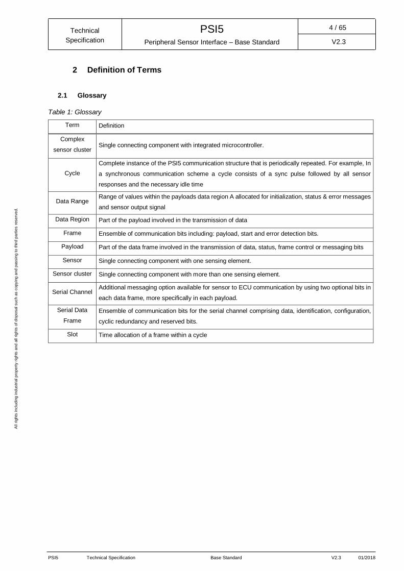
Table 1: Glossary
Term Definition
Complex
sensor cluster Single connecting component with integrated microcontroller.
Cycle
Complete instance of the PSI5 communication structure that is periodically repeated. For example, In
a synchronous communication scheme a cycle consists of a sync pulse followed by all sensor
responses and the necessary idle time
Data Range Range of values within the payloads data region A allocated for initialization, status & error messages
and sensor output signal
Data Region Part of the payload involved in the transmission of data
Frame Ensemble of communication bits including: payload, start and error detection bits.
Payload Part of the data frame involved in the transmission of data, status, frame control or messaging bits
Sensor Single connecting component with one sensing element.
Sensor cluster Single connecting component with more than one sensing element.
Serial Channel Additional messaging option available for sensor to ECU communication by using two optional bits in
each data frame, more specifically in each payload.
Serial Data
Frame
Ensemble of communication bits for the serial channel comprising data, identification, configuration,
cyclic redundancy and reserved bits.
Slot Time allocation of a frame within a cycle

PSI5 Technical Specification Base Standard V2.3 01/2018
All r
igh
ts in
clu
din
g in
dustr
ial p
rop
ert
y r
igh
ts a
nd
all r
igh
ts o
f d
isp
osal such
as c
opyin
g a
nd
passin
g t
o t
hir
d p
art
ies
rese
rve
d.
Peripheral Sensor Interface – Base Standard
PSI5 Technical
Specification
5 / 65
V2.3
2.2 Symbols / Parameters
2.2.1 General Parameters
Table 2: Symbol definitions – ECU side
Symbol /
Parameter Definition
VCE ECU output voltage present at the ECU socket pins under all conditions including dynamic load such
as noise or line effects
VCE,BASE ECU mean output voltage present at the ECU socket pins without communication (ΔIS=0) and without
synchronization pulse (static)
VE ECU internal supply voltage
Vt0 Sync slope reference voltage referenced to VCE,BASE
Vt2 Sync signal sustain voltage referenced to VCE,BASE
IE,Low Interface quiescent current tracking at ECU =∑IS, LOW
IE,LIMIT ECU current limitation
IE,LIMIT,dyn. Dynamic ECU current limitation
∑Δ(IS, LOW) Total interface quiescent current signal noise limit, i.e. sum of all sensor quiescent current signal
noises of all bus participants
LD (NEW) Dynamic Load, i.e. time that the ECU should be able to provide the current IE,LIMIT,dyn.
RE ECU total internal resistance RE = RE1 + RE2
CE ECU total internal capacitance CE = CE1 + CE2
CE1 ECU internal capacitance
CE2 ECU capacitance at ECU socket pins

PSI5 Technical Specification Base Standard V2.3 01/2018
All r
igh
ts in
clu
din
g in
dustr
ial p
rop
ert
y r
igh
ts a
nd
all r
igh
ts o
f d
isp
osal such
as c
opyin
g a
nd
passin
g t
o t
hir
d p
art
ies
rese
rve
d.
Peripheral Sensor Interface – Base Standard
PSI5 Technical
Specification
6 / 65
V2.3
Table 3: Symbol definitions – Sensor side
Symbol /
Parameter Definition
VSS Sensor input, sensor supply voltage present at the sensor socket pins including dynamic load, such
as voltage ripple and noise
VSS,BASE Mean voltage present at sensor socket pins without communication (ΔIS=0) and without
synchronization pulse (static)
VTRIG Synchronization pulse sensor trigger level threshold referenced to VSS,BASE
VEMC Margin for voltage variations of the signal on the interface line due to EMC effects
IS Quiescent current present at the sensor socket pins
|dIS/dt| Sensor quiescent current drift rate
ΔIS Sink current IS = IS,HIGH - IS,LOW used for sensor to ECU communication
Δ(IS, LOW) Interface quiescent current signal noise limit at single sensor
IS,LOW Current ‘low’ level (IS,LOW) is represented by the quiescent current present at the sensor socket pins.
IS,HIGH Current ‘high’ level (IS,HIGH) generated by the increased current sink at the sensor socket pins (IS,LOW
+ ΔIS).
RS Sensor equivalent internal resistance at sensor pins
CS Sensor equivalent internal capacitance at sensor pins
2.2.2 Communication Parameters
Table 4: Symbol definitions – ECU to sensor communication
Symbol /
Parameter Definition
TSync Duration of sync period
t0 Reference time base; Begin of phase 2 sync slope
t1 Sync signal earliest start; Delta current less than 2mA; Begin of phase 1 sync start
t2 Sync signal sustain start @Vt2; Begin of phase 3 sync sustain
t03 Sync signal sustain time; For short sync pulse [0]
t04 Discharge time; For short sync pulse [0]
t13 Sync signal sustain time; For long sync pulse [1]
t14 Discharge time; For long sync pulse [1]

PSI5 Technical Specification Base Standard V2.3 01/2018
All r
igh
ts in
clu
din
g in
dustr
ial p
rop
ert
y r
igh
ts a
nd
all r
igh
ts o
f d
isp
osal such
as c
opyin
g a
nd
passin
g t
o t
hir
d p
art
ies
rese
rve
d.
Peripheral Sensor Interface – Base Standard
PSI5 Technical
Specification
7 / 65
V2.3
Table 5: Symbol definitions – Sensor to ECU communication
Symbol /
Parameter Definition
Trise Rise time between 20% up to 80% in sink current slope
Tfall Fall time between 80% down to 20% in sink current slope
TBit Bit time for a single bit
TGap Minimum gap time which must be guaranteed between two successive data frames
tTRIG Nominal trigger detection time referenced to sensor timebase
TTRIG Trigger detection window to detect the sync pulse = tTRIG,max + Ttol_detect + TEMC
Ttol detect Tolerance time of internal trigger detection delay at sensor
TEMC Variation time of the signal on the interface line due to EMC
tnES Earliest start of frame, slot n; this is the earliest time when the transceiver or any other sensor on the
bus can expect that the frame no. n begins.
tnNS
Nominal start of frame, slot n; this is the nominal time when the sender (sensor) transmits data
according to its own internal clock. It is the nominal time when the transceiver or any other sensor on
the bus can expect that the frame, slot no. n begins.
tnNS, prog Nominal start value of frame, slot n that is programmed to the the sensor. It is derived from tn
NS by
rounding up to the next discretisation value.
tnLS Latest start of frame, slot n, this is the latest time when the transceiver or any other sensor on the bus
can expect that the frame, slot no. n begins.
tnEE Earliest end of frame, slot n, this is the earliest time when the transceiver or any other sensor on the
bus can expect that the frame, slot no. n is over.
tnNE Nominal end of frame, slot n
tnLE Latest end of frame, slot n, this is the latest time when the transceiver or any other sensor on the bus
can expect that the frame, slot no. n is over.
tSlot 1 Start Earliest start of first sensor data word
TSlot,n Maximum length of frame, slot n.
Mn No. of bits including start, data and parity or CRC bits of frame, slot n.
N No. of time slots within one sync cycle
CTn Clock tolerance of the transmitter (sensor) sending the frame no. n
2.2.3 Supply Line and Bus Parameters
Table 6: Symbol definitions – Supply Line
Symbol /
Parameter Definition
RW Wire resistance (feed & return)
RW/2 single wire resistance

PSI5 Technical Specification Base Standard V2.3 01/2018
All r
igh
ts in
clu
din
g in
dustr
ial p
rop
ert
y r
igh
ts a
nd
all r
igh
ts o
f d
isp
osal such
as c
opyin
g a
nd
passin
g t
o t
hir
d p
art
ies
rese
rve
d.
Peripheral Sensor Interface – Base Standard
PSI5 Technical
Specification
8 / 65
V2.3
Symbol /
Parameter Definition
RCE ECU connector resistance
RCS Sensor connector resistance
CW Wire capacitance (feed & return)
LW Wire inductance (feed & return)
LW/2 single wire inductance
Table 7: Symbol definitions – Bus
Symbol /
Parameter Definition
RW,Total Overall line resistance in asynchronous mode or for each wire ‘n’ in parallel bus mode
sum of ECU connector resistance, wire resistance and sensor connector resistances
CB Bus capacitance ∑CS
CBus Overall capacitive bus load CBus = CE + CB; CW not included
CL Bus load capacitance at device under test
∑(LW) Bus inductance; sum of all wire inductances
NS Number of sensors in bus
2.3 Acronyms, Abbreviations
Table 8: Acronyms, Abbreviations
Symbol /
Parameter Definition
ASIC Application Specific Integrated Circuit
ECU Electronic Control Unit
CRC Cyclic redundancy check
LSB Least significant bit
MSB Most significant bit
DUT Device Under Test
PSI5 Technical Specification Base Standard V2.3 01/2018
All r
igh
ts in
clu
din
g in
dustr
ial p
rop
ert
y r
igh
ts a
nd
all r
igh
ts o
f d
isp
osal such
as c
opyin
g a
nd
passin
g t
o t
hir
d p
art
ies
rese
rve
d.
Peripheral Sensor Interface – Base Standard
PSI5 Technical
Specification
9 / 65
V2.3
3 Data Link Layer
3.1 Sensor to ECU Communication
3.1.1 Data Frames
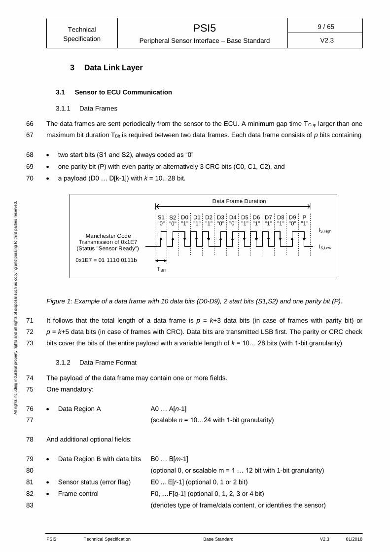
The data frames are sent periodically from the sensor to the ECU. A minimum gap time TGap larger than one 66
maximum bit duration TBit is required between two data frames. Each data frame consists of p bits containing 67
two start bits (S1 and S2), always coded as “0” 68
one parity bit (P) with even parity or alternatively 3 CRC bits (C0, C1, C2), and 69
a payload (D0 … D[k-1]) with k = 10.. 28 bit. 70
Figure 1: Example of a data frame with 10 data bits (D0-D9), 2 start bits (S1,S2) and one parity bit (P).
It follows that the total length of a data frame is p = k+3 data bits (in case of frames with parity bit) or 71
p = k+5 data bits (in case of frames with CRC). Data bits are transmitted LSB first. The parity or CRC check 72
bits cover the bits of the entire payload with a variable length of k = 10… 28 bits (with 1-bit granularity). 73
3.1.2 Data Frame Format
The payload of the data frame may contain one or more fields. 74
One mandatory: 75
Data Region A A0 … A[n-1] 76
(scalable n = 10…24 with 1-bit granularity) 77
And additional optional fields: 78
Data Region B with data bits B0 … B[m-1] 79
(optional 0, or scalable m = 1 … 12 bit with 1-bit granularity) 80
Sensor status (error flag) E0 ... E[r-1] (optional 0, 1 or 2 bit) 81
Frame control F0, …F[q-1] (optional 0, 1, 2, 3 or 4 bit) 82
(denotes type of frame/data content, or identifies the sensor) 83
S1"0"
D1"1"
D2"1"
D3"0"
D4"0"
D5"1"
S2"0"
D6"1"
D7"1"
D0"1"
P"1"
Data Frame Duration
TBIT
IS,High
IS,Low
Manchester CodeTransmission of 0x1E7
(Status "Sensor Ready")
0x1E7 = 01 1110 0111b
D8"1"
D9"0"

PSI5 Technical Specification Base Standard V2.3 01/2018
All r
igh
ts in
clu
din
g in
dustr
ial p
rop
ert
y r
igh
ts a
nd
all r
igh
ts o
f d
isp
osal such
as c
opyin
g a
nd
passin
g t
o t
hir
d p
art
ies
rese
rve
d.
Peripheral Sensor Interface – Base Standard
PSI5 Technical
Specification
10 / 65
V2.3
Serial messaging channel M0, M1 (optional 0 or 2 bit, see also Chapter 3.1.4) 84
Each optional field can be omitted in total or varied in bit length, but, if applied, the specific hierarchy of the 85
fields must be kept as shown in Figure 2. 86
Figure 2: Different parts of the PSI5 data frame
Table 9: Different parts of the payload
Bits Function Number of bits Comment
M0, M1 Messaging 0, 2 Serial messaging channel (optional)
F0 … F[q-1] Frame control 0, 1, 2, 3, 4 (optional)
E0 … E[r-1] Status 0, 1, 2 (optional)
B0 … B[m-1] Data 0, 1, 2, … , 12 Data Region B (optional)
A0 … A[n-1] Data 10, … , 24 Data Region A (mandatory)
3.1.3 Scaling of Sensor Output (for data words longer than 10 bit)
The sensor output signal range scales with the data word length n, whereas status and initialization data words 87
for frames with a payload data region of more than 10 bits still are sent in 10 bit codes of data range 2 and 3. 88
Hence, during Initialization with the data range method, the first 10 MSB bits of data are always used for 89
signaling as defined in Chapter 5.2. The remaining data bits of the payload (either A[0]…A[n-10] or an optional 90
Data Region B) are free to use. 91
The following parts of the payload are not affected by signaling range definition: 92
Remaining bits above 10 of Data Region A (A[0]...A[n-10]) 93
Data Region B (optional) 94
Serial messaging Channels (optional) 95
Frame control (optional) 96
Status (optional) 97
Payload (k=10..28 bit)
Start bits2 bit
Messaging optional0, 2 bit
Frame controloptional
0, 1, 2, 3, 4 bit
StatusOptional
0, 1, or 2 bit
Data Region B(optional)
m = 0...12 bit1 bit granularity
Data Region A n = 0...24 bit
1 bit granularity
CRC or parity1, 3 bit
D0 D1 D2 D[k-3] D[k-2] D[k-1]
Data
LS
B
Data
MS
B
CR
C M
SB
CR
C L
SB
Data Frame p= 13..33 bit
S1 S2 M0 M1 F0 ... F[q-1] E0 E[r-1] B0 B1 ... B[m-1] A0 A[n-3] ... A[n-2] A[n-1] C2 C1 C0

PSI5 Technical Specification Base Standard V2.3 01/2018
All r
igh
ts in
clu
din
g in
dustr
ial p
rop
ert
y r
igh
ts a
nd
all r
igh
ts o
f d
isp
osal such
as c
opyin
g a
nd
passin
g t
o t
hir
d p
art
ies
rese
rve
d.
Peripheral Sensor Interface – Base Standard
PSI5 Technical
Specification
11 / 65
V2.3
Figure 3: Scaling of data range
3.1.4 Serial Channel
In addition to Data Regions A and B, information can be sent via a serial channel. In this case, the serial 98
message frame stretches over 18 consecutive PSI5 data messages from the transmitter as shown below. All 99
18 frames must be successfully transmitted for the serial value to be received. The messaging bit M1 of sensor 100
frame No. 8 determines the serial format (12bit data field with 8bit ID or 16bit data field with 4bit ID). In 101
synchronous operation the serial data frame, or its constituent messaging bits, respectively, is assigned to the 102
related time slot of the corresponding data frame. 103
S1 S2 M0 M1 F0 F1 F2 F3 E0 E1 B0 B1 Bm-1 An-10 An-9 An-8 An-7 An-1 C2 C1 C0
D5 D6 D7 D8 D9 D10 D14 D15 C2 C1 C0D0 D1 D2 D3 D4S1 S2 D11 D12 D13
Free to use
LSB
Fixed Signaling Range
MSB
Start bits
2 bit
Payload
(only Data Region A)
CRC or parity
1, 3 bit
Payload
Start bits
2 bit
Messaging
optional
0, 2 bit
Frame control
optional
0, 1, 2, 3, 4 bit
Status
Optional
0, 1, 2, 3 bit
Data Region B
(optional)10 bit out of Data Region A
CRC or parity
1, 3 bit
Application specific extension
independent of signaling codes
Free use of rest of Payload in case
Of signaling codes63 Signaling codes defined for first 10 MSBs of data
63 Signaling codes defined for first 10 MSBs of data

PSI5 Technical Specification Base Standard V2.3 01/2018
All r
igh
ts in
clu
din
g in
dustr
ial p
rop
ert
y r
igh
ts a
nd
all r
igh
ts o
f d
isp
osal such
as c
opyin
g a
nd
passin
g t
o t
hir
d p
art
ies
rese
rve
d.
Peripheral Sensor Interface – Base Standard
PSI5 Technical
Specification
12 / 65
V2.3
Figure 4: Serial data frame generated by the two messaging bits of the sensor data frame (messaging channel)
3.2 ECU to Sensor Communication
3.2.1 Data Frames
The frames for the ECU to sensor communication are composed by 104
A specific start condition, enabling secure detection of the frame start even after loss of synchronization 105
A data field 106
A checksum to ensure data integrity 107
Transmission of a correct ECU to Sensor data frame does not have to be acknowledged in general. However, 108
if required by the application, the sensor may send an optional response to the ECU by either transmitting a 109
return code and return data out of the reserved data range area or via the serial channel’s messaging bits. 110
ECU to Sensor data frames are structured as described in following chapters. They are applied in different 111
ways for the two different bit coding method in use (Tooth Gap or Pulse Width method). A combined usage of 112
bit coding method and their respective frame types is not allowed in order to ensure safe data recognition. 113
Specific regulations must be given in the corresponding Substandards or specific product specifications. 114
3.2.2 Frame Formats - Tooth Gap method
The Tooth Gap method is limited to usage of data frame formats 1-3. Frame formats 1-3 are composed by 115
three start bits, a data field containing the sensor address, function code and data and a three bit CRC. Sensor 116
response may be sent in data range format within the following two or three sync periods. Three data field 117
lengths are available, “short”, “long” and “xlong”. 118
Payload (10..28 bit)
S1 S2 M0 M1 F0 F1 F2 F3 E0 E1 B0 B1 . . . Bm-1 A0 A1 A2 A3 An-1 C2 C1 C0A4 A5 A6 A7 . . .
Start bits
2 bit
Messaging
optional
0, 2 bit
Frame control
optional
0, 1, 2, 3, 4 bit
Status
optional
0, 1, 2, 3 bit
Data Region B
(optional)
Data Region A
(10..24 bit)
CRC or parity
1, 3 bit
Frame No.
Serial data (bit M1)
Serial data (bit M0)
1 2 3 4 5 6 7 8 9 10 11 12 13 14 15 16 17 18
1 1 1 1 1 1 0 0 Serial ID (7-4) 0 Serial ID (3-0) 0
6-bit checksum (5-0) Data field (11-0)
Frame No.
Serial data (bit M1)
Serial data (bit M0)
1 2 3 4 5 6 7 8 9 10 11 12 13 14 15 16 17 18
1 1 1 1 1 1 0 1 Serial ID (3-0) 0 Data field (15-12) 0
6-bit checksum (5-0) Data field (11-0)
Serial data frame
Configuration bit (12 bit data with 8 bit ID or 16 bit data with
4 bit ID)
PSI5 frame #1
PSI5 frame #2
PSI5 frame #3

PSI5 Technical Specification Base Standard V2.3 01/2018
All r
igh
ts in
clu
din
g in
dustr
ial p
rop
ert
y r
igh
ts a
nd
all r
igh
ts o
f d
isp
osal such
as c
opyin
g a
nd
passin
g t
o t
hir
d p
art
ies
rese
rve
d.
Peripheral Sensor Interface – Base Standard
PSI5 Technical
Specification
13 / 65
V2.3
Figure 5: ECU to sensor communication with Tooth Gap method
The start condition for an ECU to sensor communication consists of either at least five consecutive logical 119
zeros or at least 31 consecutive logical ones. The sensor responds with the standard sensor to ECU current 120
communication in its corresponding time slot. “Sync Bits” (logical “1”) are introduced at each fourth bit position 121
in order to ensure a differentiation between data content and start condition and to enable sensor 122
synchronization when using the tooth gap method. The data frame length is defined by the content of the 123
Sensor Address (SAdr) and the function Codes (FC) as shown in Figure 6. The calculation of the three bit 124
checksum is given in Chapter 3.3.2. 125
Figure 6: Data frames 1-3 for ECU to sensor communication with Tooth Gap method
3.2.3 Frame Formats – Pulse Width method
Pulse Width method uses frame format 4. Data frame 4 is composed by nine start bits, a three bit sensor 126
address field, a configuration bit, a 20-bit data field containing application specific data and a six bit CRC. 127
“Stuffing Bits” (logical “0”) are introduced at each seventh bit position (eight bit position for start region) in order 128
to ensure a differentiation between data content and frame start. Transmission of a correct ECU to Sensor 129
data frame does not have to be acknowledged in general. However, if required by the application, the sensor 130
may send a response to the ECU by either transmitting a return code and return data out of the reserved data 131
1 1 0 1 0 1 1 1
RC RD1 RD2
Start Condition Start Bits Data Field CRC Sensor Response
S Synchronisation Bit [1]0 S1 0
Start
A0 SA1 A2
Sadr
F0 SF1 F2
FC
C0C2 C1
CRC
Frame 1 „Short“
N° Bits: 15+2 (8.5ms @ 500µs)
RC RD1
Resp
N° Bits: 29+3 (16ms @ 500µs); Address / Data Range: 64 x 4 Bit
0 S1 0
Start
A0 SA1 A2
SAdr
F0 SF1 F2
FC
X0 SX1 X2 X3 SX4 X5 D0 D1 D3D2 S C2 C0C1 S
CRC
RC RD1 RD2
RAdr Data Resp
Frame 2a „Long“ (4-Bit Data Nibbles)
0 S1 0
Start
S
SAdr
F0 SF1 F2
FC RAdr
S S S S
CRCData Resp
Frame 2b „Long“ (8-Bit Data Word)
N° Bits: 29+3 (16ms @ 500µs); Address / Data Range: 4 x 8 Bit
RC RD1 RD2X0 X1 D0 D1 D2 D3 D4 D5 D7D6 C2 C0C1A0 A1 A2
0 S1 0
Start
S
SAdr
S
FC
X0-X7 + Sync Bits D0-D7 + Sync Bits
CRCRAdr Data Resp
Frame 3 „XLong“
N° Bits: 37+3 (20ms @ 500µs); Address / Data Range: 256 x 8 Bit
F0 F1 F2A0 A1 A2 S C0C1C2 RC RD1 RD2

PSI5 Technical Specification Base Standard V2.3 01/2018
All r
igh
ts in
clu
din
g in
dustr
ial p
rop
ert
y r
igh
ts a
nd
all r
igh
ts o
f d
isp
osal such
as c
opyin
g a
nd
passin
g t
o t
hir
d p
art
ies
rese
rve
d.
Peripheral Sensor Interface – Base Standard
PSI5 Technical
Specification
14 / 65
V2.3
range area or via the serial channel’s messaging bits. All function codes and frame data content of frame 132
formats 1-3 can also be transmitted with frame format 4 and Pulse Width method, as describes in the next 133
section. 134
Figure 7: ECU to sensor communication with Pulse Width method
Figure 8: Data frame 4 for ECU to sensor communication with Pulse Width method
3.2.4 Mapping of Data frames for Pulse Width method
In case the function codes as defined in Chapter 5.3 shall be used in combination with frame 4 and Pulse 135
Width method, they shall be mapped as shown below. 136
0 1 1 0
Start BitsSensor Address and
Data Field6-bit CRC
Sensor Response
via serial
messaging or RC /
RD1 / RD2
1
Sensor
Data
Start Sadr Data CRC
S 1 1 1 1 1 1 1 S A0 C S D8-D19+Stuffing Bits
S
C
A1 A2 D0 D1 D2 ... D7 S S C0 C1 C2 C3 C4 C5
Stuffing Bit [0]
Configuration Bit[1] Mapping of frames 1-3[0] all other applicationsFrame 4 „XXLong“
N° Bits: 43 (21.5ms @ 500μs)
PSI5 Technical Specification Base Standard V2.3 01/2018
All r
igh
ts in
clu
din
g in
dustr
ial p
rop
ert
y r
igh
ts a
nd
all r
igh
ts o
f d
isp
osal such
as c
opyin
g a
nd
passin
g t
o t
hir
d p
art
ies
rese
rve
d.
Peripheral Sensor Interface – Base Standard
PSI5 Technical
Specification
15 / 65
V2.3
Figure 9: Mapping of frames 1-3 into frame 4
3.3 Error Detection
Error detection is embedded into all messaging schemes within PSI5. For sensor to ECU communication a 137
single bit even parity (for example for 10 bit data words) or a 3 bit CRC (intended for longer data words) is 138
used. In this case the 3 bit CRC comprises all payload bits (D[0] … D[k-1], see Figure 10). In addition the 3 bit 139
CRC is also used for ECU to sensor communication for those frames using tooth-gap method. For both the 140
serial channel in sensor to ECU communication and the pulse width method in ECU to sensor communication 141
a 6 bit CRC is used. 142
3.3.1 Parity Bit
One error detection alternative is the use of a parity bit to verify the payload content. Here, even parity is used. 143
It is intended for use in shorter data words, i.e. 10 bit data words, and excludes the start bits. 144
3.3.2 3 bit CRC
The generator polynomial of the CRC is g(x)= x3+x+1 with a binary CRC initialization value “111” (MSB first) 145
and the data bits extended by three zeros (as MSBs). This augmented data word shall be fed (LSB first) into 146
the shift registers of the CRC check. Start bits are ignored in this check. When the last zero of the augmentation 147
is pending on the input adder, the shift registers contain the CRC checksum. These three check bits shall be 148
transmitted in reverse order (MSB first: C2, C1, C0). 149
S
C
Stuffing Bit [0]
Configuration Bit[1] Mapping of frames 1-3
Frame 1 mapped into frame 4
Start Sadr Data CRC
S 1 ... 1 S F0 F2 0F1 S 0 0 0 0 S 0 0 C0 ... C5A0 A1 A2 1 0 ... 0 0 S 0 S...
Start Sadr Data CRC
S 1 ... 1 S F0 F2 X2F1 S X0 X1 X3 X4 S X5 0 C0 ... C5A0 A1 A2 1 D0 ... D3 0 S 0 S...
Frame 2 (4-Bit Data Nibbles) mapped into frame 4
Frame 2 (8-Bit Data Word) mapped into frame 4
Start Sadr Data CRC
S 1 ... 1 S F0 F2 D0F1 S X0 X1 D1 D2 S D3 0 C0 ... C5A0 A1 A2 1 D7 0 S 0 S......
Frame 3 mapped into frame 4
Start Sadr Data CRC
S 1 ... 1 S F0 F2F1 S X0 X4 S X6 0 C0 ... C5A0 A1 A2 1 D1 D2 S D3 S... X5 X7 D0 ... D7

PSI5 Technical Specification Base Standard V2.3 01/2018
All r
igh
ts in
clu
din
g in
dustr
ial p
rop
ert
y r
igh
ts a
nd
all r
igh
ts o
f d
isp
osal such
as c
opyin
g a
nd
passin
g t
o t
hir
d p
art
ies
rese
rve
d.
Peripheral Sensor Interface – Base Standard
PSI5 Technical
Specification
16 / 65
V2.3
Figure 10: Bit Data word example with 3-Bit CRC
3.3.3 6 bit CRC
The generator polynomial of the 6bit checksum is g(x)= x6+x4+ x3+1 with a binary initialization value “010101” 150
(MSB first). In the case of sensor to ECU serial communication the CRC value is derived from the serial 151
messaging contents of sensor frame 7 to 18, the bits are read into a newly generated message data word 152
starting with the serial Data bit M0 of sensor frame 7 and ending with the serial data bit M1 of sensor frame 153
18. The reading order is illustrated in Figure 11. For ECU to sensor communication the start bits and stuffing 154
bits are ignored in this check. 155
For CRC generation the transmitter extends the message data by six zeros. This augmented data word shall 156
be fed (LSB first) into the shift registers of the CRC check. When the last zero of the augmentation is pending 157
on the input adder, the shift registers contain the CRC checksum. For sensor to ECU serial communication 158
these six check bits shall be transmitted MSB first [C5, C4, ... C0]. An example is given in Figure 12. In the 159
case of ECU to sensor communication via pulse width method these six check bits shall be transmitted LSB 160
first [C0, C1 .. C5]. 161
S1 S2 D0 D1 D2 D3 D4 D5 D6 D7 D8 D9 D10 D11 D12 D13 D14 D15 C2 C1 C0
0 0 0 0 1 1 0 1 0 0 1 0 1 1 0 1 0 1 1 0 0
C=“1100“ 2=“0010“ D=“1101“ A=“1010“
Example: 16-bit data word „0xAD2C“ with 3-bit CRC
CRC Calculation Scheme input
dataT T T
C0 C1 C2
1*1 + 1*X + 0*X2 + 1*X3 = X3 + X + 1

PSI5 Technical Specification Base Standard V2.3 01/2018
All r
igh
ts in
clu
din
g in
dustr
ial p
rop
ert
y r
igh
ts a
nd
all r
igh
ts o
f d
isp
osal such
as c
opyin
g a
nd
passin
g t
o t
hir
d p
art
ies
rese
rve
d.
Peripheral Sensor Interface – Base Standard
PSI5 Technical
Specification
17 / 65
V2.3
Figure 11: Reading order for checksum generation in sensor to ECU serial communication
Figure 12: Example for checksum generation, 12-Bit data field, 8-Bit message ID and 6-Bit CRC for sensor to
ECU serial communication channel
Sensor FrameFrame No.
Serial Data (bit M1)
Serial Data (bit M0)
1 2 3 4 5 6 7 8 9 10 11 12 13 14 15 16 17 18
1 3 5 7 9 11 13 15 17 19 21 23
0 2 4 6 8 10 12 14 16 18 20 22
Messaging bits for checksum calculation
Bit receive No.
Serial Data (bit M1)
Serial Data (bit M0)
1 2 3 4 5 6 7 8 9 10 11 12 13 14 15 16 17 18
0 0 0 0 1 0 0 0 0 1 1 0
0 0 1 0 1 1 1 0 0 1 0 1
1 1 1 1 1 1
C51
C40
C30
C21
C11
C01
ID = 0x23 Data = 0x2E5
D6 D7 D8 D9 D10 D11 D12 D13 D14 D15 D16 D17 D18 D19 D20 D21 D22 D23
1 0 0 0 0 0 1 1 0 1 1 00 0 1 1 1 0
D0 D1 D2 D3 D4 D5
0 0 0 0 1 0
Shift data:
input data
T T
C0 C1
1*1 + 0*X + 0*X2 + 1*X3 + 1*X4 + 0*X5 + 1*X6 = X6 + X4 + X3 + 1
T
C2
T T T
C3 C4 C5
CRC Calculation Scheme:
PSI5 Technical Specification Base Standard V2.3 01/2018
All r
igh
ts in
clu
din
g in
dustr
ial p
rop
ert
y r
igh
ts a
nd
all r
igh
ts o
f d
isp
osal such
as c
opyin
g a
nd
passin
g t
o t
hir
d p
art
ies
rese
rve
d.
Peripheral Sensor Interface – Base Standard
PSI5 Technical
Specification
18 / 65
V2.3
4 Physical Layer
4.1 General
The sensors are connected to the ECU by just two wires, using the same lines for power supply and data 162
transmission. The ECU integrated transceiver provides a pre-regulated voltage to the sensors and reads in 163
the transmitted sensor data. The transmission of sensor data to the ECU is done by the means of current 164
modulation. An optional pulse modulation on the supply voltage from the ECU to the sensors can be used to 165
synchronize sensor data transmission and to transmit data from the ECU to the sensor. For 125kbps all 166
maximum and minimum values are specified. Implementations at other data rates, such as 189 Kbps are 167
however possible but have to be validated on system level. Large cable lengths / inductances may require 168
appropriate selection of sensor and ECU capacitance values and / or additional damping measures. 169
4.2 Supply Line Model
PSI5 usually uses twisted pair lines which are modeled as shown in Figure 13. Parameter specification is done 170
separately for the different system configurations. All parameters are based on a maximum supply line length 171
of 12m under assumption of standard CAN cable with a maximum inductance of 0.72µH/m and maximum 172
capacitance of 50 pF/m. This maximum length, however, is only an indication. Depending on the wiring harness 173
and system configuration the maximum length might vary. 174
Figure 13: Supply line model for PSI5
Table 10: Parameter specification for supply line model
N° Parameter Symbol Conditions/Remark Min Typ Max Unit
1 ECU Connector resistance RCE (0.2) Ω
2 Sensor Connector resistance RCS (0.2) Ω
3 Single wire resistance RW/2 (0.5) Ω
4 Overall line resistance incl. wire &
connector RW,Total 2 * (RCE +RW/2+RCS) 0.1 2.5 Ω
5 Wire inductance LW 2 * (LW / 2) 8.7 µH
6 Wire capacitance CW 600.0 pF
RCE RW /2 LW /2
RW /2 LW /2RCE
RCS
RCS
CW
PSI5 Technical Specification Base Standard V2.3 01/2018
All r
igh
ts in
clu
din
g in
dustr
ial p
rop
ert
y r
igh
ts a
nd
all r
igh
ts o
f d
isp
osal such
as c
opyin
g a
nd
passin
g t
o t
hir
d p
art
ies
rese
rve
d.
Peripheral Sensor Interface – Base Standard
PSI5 Technical
Specification
19 / 65
V2.3
4.3 Single Sensor, Point to Point Topologies
4.3.1 Single Sensor, Point to Point Asynchronous Topologies (PSI5-A)
PSI5-A describes a point-to-point connection for unidirectional, asynchronous data transmission. 175
Each sensor is connected to the ECU by two wires to a dedicated interface of the transceiver. After switching 176
on the power supply, the sensor starts transmitting data to the ECU periodically. Timing and repetition rate of 177
the data transmission are controlled by the sensor. 178
Figure 14: Single sensor configuration (simplified diagram)
4.3.2 Parameter Specification for Single Sensor Configuration
Table 11: Parameter specification for single sensor configuration
N° Parameter Symbol Conditions/Remark Min Typ Max Unit
1 ECU total internal capacitance
CE= CE1 +CE2 CE 6.0 47 nF
2
Sensor equivalent internal capacitance CS @ 10…200kHz 6.0 47 nF
3 @ 200kHz…2MHz 1.32 47 nF
4 ECU total internal resistance
RE = RE1 +RE2 RE
Standard 5 12.5 Ω
5 Advanced 5 9.5 Ω
6 Sensor equivalent internal resistance RS 2.5 Ω
4.4 Multi Sensor, Bus Topologies
4.4.1 Synchronous Parallel Bus Mode (PSI5-P)
PSI5-P describes a bus configuration for synchronous data transmission of one or more sensors connected to 179
a single interface of the transceiver within the ECU. 180
Each sensor is connected to the ECU by a separate pair of wires (star topology). 181
VE Supply LineCE1
RE1 RE2
CE2
ECU Sensor
CS ISink
VCE VSS

PSI5 Technical Specification Base Standard V2.3 01/2018
All r
igh
ts in
clu
din
g in
dustr
ial p
rop
ert
y r
igh
ts a
nd
all r
igh
ts o
f d
isp
osal such
as c
opyin
g a
nd
passin
g t
o t
hir
d p
art
ies
rese
rve
d.
Peripheral Sensor Interface – Base Standard
PSI5 Technical
Specification
20 / 65
V2.3
Figure 15: Synchronous parallel bus mode (simplified schematic)
In order to provide an interchangeability of different sensor and transceiver components, additional interface 182
parameters for ECU, sensors, and wiring are specified for this bus mode in Chapter 4.4.4. 183
4.4.2 Synchronous Universal Bus Mode (PSI5-U)
PSI5-U describes a bus configuration for synchronous data transmission of one or more sensors connected 184
to a single interface of the transceiver within the ECU. 185
The sensors can be connected to the ECU in different wiring topologies including splices or pass-through 186
configurations. In all cases the total supply line, i.e. sum of all supply lines, shall not exceed the maximum 187
values given in Table 12. 188
CE1
RE1 RE2
CE2
VE
ECU
Supply LineCS ISink
VSS
Sensor1
Supply LineCS ISink
VSS
Sensor2
VCE
VCE
Supply LineCS ISink
VSS
Sensor3VCE

PSI5 Technical Specification Base Standard V2.3 01/2018
All r
igh
ts in
clu
din
g in
dustr
ial p
rop
ert
y r
igh
ts a
nd
all r
igh
ts o
f d
isp
osal such
as c
opyin
g a
nd
passin
g t
o t
hir
d p
art
ies
rese
rve
d.
Peripheral Sensor Interface – Base Standard
PSI5 Technical
Specification
21 / 65
V2.3
Figure 16: Example for a pass-through configuration (simplified schematic)
Figure 17: Example for a splice configuration (simplified schematic)
The wiring and sensors are considered as a “black box” resulting in a limited interchangeability of sensor and 189
transceiver components. Interface parameters in Chapter 4.4.4 are given for the ECU and the “black box” only. 190
4.4.3 Synchronous Daisy Chain Bus Mode (PSI5-D)
PSI5-D describes a bus configuration for synchronous data transmission of one or more sensors connected in 191
a daisy chain configuration to a single interface of the transceiver within the ECU. 192
VEVCE
Sensor1
CS ISink
VSSSupply Line
Sensor2
CS ISink
VSSSupply Line
Sensor3
CS ISink
VSSSupply Line
ECU
CE1
RE1 RE2
CE2
Sensor1
Sensor2
Sensor3
VE
ECU
CE1
RE1 RE2
CE2
Supply Line
VCE
CS ISinkSupply Line
VSS
CS ISinkSupply Line
VSS
CS ISinkSupply Line
VSS

PSI5 Technical Specification Base Standard V2.3 01/2018
All r
igh
ts in
clu
din
g in
dustr
ial p
rop
ert
y r
igh
ts a
nd
all r
igh
ts o
f d
isp
osal such
as c
opyin
g a
nd
passin
g t
o t
hir
d p
art
ies
rese
rve
d.
Peripheral Sensor Interface – Base Standard
PSI5 Technical
Specification
22 / 65
V2.3
The required addressing of the sensors during start up is specified in Chapter 5.3.2. Interface parameters for 193
ECU, sensors, and wiring are specified in Chapter 4.4.4. 194
Figure 18: Synchronous daisy chain bus (simplified schematic)
4.4.4 Parameter Specification for Bus Topologies
Table 12: Parameter specification for bus topologies
N° Parameter Symbol Conditions/Remark Min Typ Max Unit
1* ECU total internal capacitance
CE = CE1 +CE2 CE 15 35 nF
2*
Sensor (equivalent) internal capacitance CS @ 10…200kHz 9 24 nF
3* @ 200kHz…2MHz 1.32 24 nF
4 Bus capacitance CB CB=∑CS 9 72 nF
5* Overall capacitive bus load CBus CBus=CE+CB 24 107 nF
6 ECU total internal resistance
RE = RE1 +RE2 RE
Standard 5 12.5 Ω
7 Advanced 5 9.5 Ω
8 Sensor (equivalent) internal resistance RS 2.5 Ω
9 Bus inductance ∑(LW)
Sum of all wire
inductance:
∑(2 * (LW / 2))
8.7 µH
1*) Damping is required in ECU to limit oscillations on the bus lines. 195
2-3*) Maximum value for CS is given for an out of context design; If system integration requires it CS for single sensors 196
can be exceeded but max Bus capacitance CB shall not be violated and system design shall ensure proper 197
signal behavior 198
5*) Wire capacitance CW not included due to negligible value 199
VE
VCE VSSSupply Line
VSSSupply Line
VSSSupply Line
ECU
CE1
RE1 RE2
CE2
Sensor 1
ISinkCS
RDS On
Sensor 2
ISinkCS
RDS On
Sensor 3
ISinkCS
RDS On
PSI5 Technical Specification Base Standard V2.3 01/2018
All r
igh
ts in
clu
din
g in
dustr
ial p
rop
ert
y r
igh
ts a
nd
all r
igh
ts o
f d
isp
osal such
as c
opyin
g a
nd
passin
g t
o t
hir
d p
art
ies
rese
rve
d.
Peripheral Sensor Interface – Base Standard
PSI5 Technical
Specification
23 / 65
V2.3
4.5 Sensor to ECU Communication
Data transmission from the sensor to the ECU is realized by current modulation of the power supply by a 200
sensor internal controlled source. Resulting supply line current oscillations are damped by the ECU and sensor 201
input impedances. An exemplary sensor to ECU communication is shown in the figure below on the basis of 202
the sensor current IS. 203
A "low" level (IS,LOW) is represented by the normal (quiescent) current consumption of the sensor. 204
A "high" level (IS,HIGH) is generated by an increased current sink of the sensor (IS,LOW + IS). 205
The current modulation is then detected within the transceiver ASIC as a manchester coded stream, where a 206
logic "0" is represented by a rising slope and a logic "1" by a falling slope of the current in the middle of TBit 207
(see PSI5 data link layer definition). 208
Figure 19: Bit encoding and data frame timing for sensor to ECU communication
Table 13: Parameter specification of sensor to ECU communication (related to the sensor)
N° Parameter Symbol Conditions/Remark Min Typ Max Unit
1* Bit time (based on Standard clock
tolerance) TBit
125kbps mode 7.6 8.0 8.4 µs
2* 189kbps mode 5.0 5.3 5.6 µs
3* Clock tolerance of the transmitter
(sensor) CT Standard 5 %
4* Sensor clock deviation during data
frame (see Substandard) CDS
Standard 1 %
5* Legacy 0.1 %
6
Gap time TGap
125kbps mode; TGap >
TBit 8.4 µs
7 189kbps mode; TGap >
TBit 5.6
8* Rise Time Current Slope TRISE 20%..80% (of Is) (0.33) (1.0) µs
9* Fall Time Current Slope TFALL 80%..20% (of Is) (0.33) (1.0) µs
IS, High
IS, Low
TBit TGap
∆IS
Data Frame 2
t
IS
IS, Threshold

PSI5 Technical Specification Base Standard V2.3 01/2018
All r
igh
ts in
clu
din
g in
dustr
ial p
rop
ert
y r
igh
ts a
nd
all r
igh
ts o
f d
isp
osal such
as c
opyin
g a
nd
passin
g t
o t
hir
d p
art
ies
rese
rve
d.
Peripheral Sensor Interface – Base Standard
PSI5 Technical
Specification
24 / 65
V2.3
N° Parameter Symbol Conditions/Remark Min Typ Max Unit
10* Mark/Space Ratio MSR
@ Sensor
(tfall, 80 - trise, 20) / TBit
(tfall, 20 - trise, 80) / TBit
47 50 53 %
11 Maximum clock drift rate CT 1 %/sec
1,2*) corresponding to a standard clock tolerance of the transmitter CT 209
3*) Advanced clock tolerance refers to tighter clock tolerances needed for longer messages (see Chassis and 210
Safety Substandard). 211
4,5 *) @ maximum temperature gradient and maximum frame length; the overall clock tolerance of the transmitter 212
must not be exceeded. 213
8,9*) Small rise and fall times lead to increased radiated emission. Different definitions may apply for Universal Bus 214
and Daisy Chain Bus. Parameters in brackets are given as a hint for the sensor development. Tighter tolerances 215
might apply to the current sink in the transmitter.) 216
4.6 ECU to Sensor Communication
While the sensor to ECU communication is realized by current signals, voltage modulation on the supply lines 217
is used to communicate with the sensors. The PSI5 “sync signal” is used for the sensor synchronization in all 218
synchronous operation modes and also as physical layer for bidirectional communication. 219
ECU to Sensor communication is performed according to either the so called Tooth Gap or Pulse Width method 220
as defined hereafter. 221
4.6.1 Tooth Gap method
A logical “1” is represented by the presence of a regular (“short”) sync signal, a logical “0” by the absence of 222
the sync signal at the expected time window of the sync signal period. The voltage for a logical “0” must remain 223
below the sync slope reference voltage Vt0 specified as the sync signal t0 start condition. 224
Figure 20: Bit encoding according to the Tooth Gap method
This bit encoding method is only applicable with a fixed sync signal period. 225
4.6.2 Pulse Width method
A logical “0” is represented by the presence of the regular (“short”) PSI5 sync signal, a logical “1” by a longer 226
sync signal (see Chapter 4.9) 227
1 1 1 10 0 0

PSI5 Technical Specification Base Standard V2.3 01/2018
All r
igh
ts in
clu
din
g in
dustr
ial p
rop
ert
y r
igh
ts a
nd
all r
igh
ts o
f d
isp
osal such
as c
opyin
g a
nd
passin
g t
o t
hir
d p
art
ies
rese
rve
d.
Peripheral Sensor Interface – Base Standard
PSI5 Technical
Specification
25 / 65
V2.3
Figure 21: Bit encoding via Pulse Width method
4.7 General Parameters
In this section an overview is given of all parameters valid under all operating conditions including temperature 228
range and life time. Detailed information is given within the corresponding paragraphs of the following pages. 229
4.7.1 Supply and Communication Parameters Definitions
In Figure 22 an overview of the current and voltage behavior for both sensor and ECU is shown during ECU 230
to sensor and sensor to ECU communication. 231
Current behavior is given in terms of ECU current IE, measured at the ECU connector pins. Voltage behavior, 232
on the other hand, is given in terms of supply voltages VCE and VSS, which are the (resulting) voltages at the 233
ECU / Sensor connector pins. They include static and dynamic effects of the current modulation, where the 234
dynamic effects are originated in the dynamic sink current ∆IS through the parasitic supply line (RW, LW, CW) 235
as well as ECU (CE) and sensor (CS) internal elements leading for example to ripple voltages and noise. It 236
therefore follows that the minimum and maximum supply voltage @ sensor VSS, min and VSS, max shall not be 237
violated during any condition. Additionally, base supply voltages VCE, BASE and VSS, BASE are defined as the static 238
voltages at the ECU and sensor connector pin when no communication is taking place (i.e. no sync pulse or 239
current modulation). Here, VSS, BASE is equivalent to VCE, BASE minus the static supply voltage drops resulting 240
from interface quiescent current ILOW over the supply line resistances, where additional static voltage drops 241
over the ECU (RE) or sensor internal resistors are not included in the base supply voltages VCE, BASE and VSS, 242
BASE. 243
0 0 0 1 1

PSI5 Technical Specification Base Standard V2.3 01/2018
All r
igh
ts in
clu
din
g in
dustr
ial p
rop
ert
y r
igh
ts a
nd
all r
igh
ts o
f d
isp
osal such
as c
opyin
g a
nd
passin
g t
o t
hir
d p
art
ies
rese
rve
d.
Peripheral Sensor Interface – Base Standard
PSI5 Technical
Specification
26 / 65
V2.3
Figure 22: System current and voltage definitions
In the table below all voltage and current values are measured at the sensor's connector pins unless otherwise 244
noted. 245
Table 14: System parameter specification
N° Parameter Symbol Conditions/Remark Min Typ Max Unit
1* Supply Voltage
@ Sensor VSS
Standard Voltage 5.0 16.5 V
2* Low Voltage 4.0 16.5
3* Base supply voltage VSS, BASE Standard Voltage; 5.0 11.0 V
ECU to sensor communication Sensor to ECU communication
IE IS
IE,LIMIT
IE,LOW,max
IE,LOW,min
ΔIS
IS,LOW
ΔISIS,LOW, max
IS,LOW,min
Currents at the ECU & sensor connector pins
VCE,max
VCE,BASE
VCE,min
t
VCE VSS
VSS,max
VSS,BASE
VSS,min
Voltage ripple @ ECU
Voltage ripple @ sensor
Sync pulse
VSS
VCE
VCE,Peak,min≥VCE,min
VSS,Peak,min≥VSS,min
Voltages at the ECU & sensor connector pins

PSI5 Technical Specification Base Standard V2.3 01/2018
All r
igh
ts in
clu
din
g in
dustr
ial p
rop
ert
y r
igh
ts a
nd
all r
igh
ts o
f d
isp
osal such
as c
opyin
g a
nd
passin
g t
o t
hir
d p
art
ies
rese
rve
d.
Peripheral Sensor Interface – Base Standard
PSI5 Technical
Specification
27 / 65
V2.3
N° Parameter Symbol Conditions/Remark Min Typ Max Unit
4* @ Sensor Low Voltage 4.0 11.0
5*
Supply Voltage
@ ECU VCE
Standard Voltage 5.5 16.5
V 6* Low Voltage 4.2 16.5
7* Increased voltage 6.5 16.5
8*
Base supply voltage
@ ECU VCE, BASE
Standard voltage 5.7 11.0 V
9* Low voltage 4.4 11.0
10* Increased voltage 6.7 11.0 V
11 Sink current
@ Sensor IS
Common mode;
IS = IS, HIGH - IS, LOW 22.0 26.0 30.0 mA
12 Low power mode;
IS = IS, HIGH - IS, LOW 11.0 13.0 15.0 mA
13*
Interface quiescent current
@ Sensor IS, LOW
Standard current 4.0 19.0 mA
14 Extended current 4.0 35.0 mA
15* Daisy chain mode 4.0 12.0 mA
16* Interface quiescent current
tracking @ ECU
IE, LOW =
∑IS,LOW
Standard current 4.0 19.0 mA
17* Extended current 4.0 35.0 mA
18* Quiescent current drift rate
@Sensor |dIS/dt|
measured after 1st order high-pass
filter with corner frequency fC,1=1Hz 10 mA/sec
19* Current limitation
@ ECU IE,LIMIT
Standard current 50.0 105 mA
20* Extended current 65.0 130 mA
21* Dynamic current limitation
@ ECU IE,LIMIT,dyn.
Standard current with dynamic load
condition 65.0 mA
22* Extended current with dynamic
load condition 80.0 mA
23* signal noise limit
@ Sensor (peak to peak,
fC,1 = 1Hz < f < 5MHz = fC,2)
Δ(IS, LOW)
Standard noise limit -2 +2 mA
24* Extended noise limit -3 +3 mA
25* Reduced noise limit -1 +1 mA
26 signal noise limit
@ ECU ((Sensors)) ∑Δ(IS, LOW) sqrt(4xΔ(IS, LOW)2) +4 mA
1, 2*) In any case during normal operation VSS shall not be violated. This includes dynamic effects like ripple voltage 246
and noise. 247
7, 10*) Optional increased base supply voltage to overcome additional voltage drops in Universal Bus and Daisy Chain 248
Bus applications. 249
5-7*) To be guaranteed by the ECU at the output pins of the ECU under all specified conditions including over- and 250
undershoot due to changes in line load when in Universal Bus Mode and Daisy Chain Bus Mode. Tested as 251
defined in the ECU reference test in Chapter 4.8.1.3. 252

PSI5 Technical Specification Base Standard V2.3 01/2018
All r
igh
ts in
clu
din
g in
dustr
ial p
rop
ert
y r
igh
ts a
nd
all r
igh
ts o
f d
isp
osal such
as c
opyin
g a
nd
passin
g t
o t
hir
d p
art
ies
rese
rve
d.
Peripheral Sensor Interface – Base Standard
PSI5 Technical
Specification
28 / 65
V2.3
13-15*) When implemented in a bus configuration IS, LOW will determine the number of sensors allowed as limited by the 253
maximum Quiescent current @ECU 254
15*) In Daisy Chain Bus Mode the quiescent current limitations apply for a single sensor. 255
16-17*) Range of tracked current supply for sensor. 256
17*) Extended current range for higher current consumption e.g. in bus or sensor cluster configurations. 257
21, 22*) Dynamic load condition: The ECU must have the capability to provide the current IE,LIMIT,dyn for tSET1. For Daisy 258
Chain Bus Mode this current has to be provided for at least 10ms when a sensor is powered on (see Table 22). 259
23-25*) Parameters denote the sum over all bus participants. ILOW is the (initial and average) quiescent current of the 260
bus. Over lifetime and temperature, the quiescent current may vary but must not exceed the limits for ILOW. 261
Means for an adaptive current threshold may be required in the transceiver in order to cope with varying 262
quiescent currents, especially when connected in bus systems. Data loss of the whole system as a consequence 263
of an abrupt quiescent current drift after loss of one sensor connection also needs to be considered. 264
24*) For complex sensor clusters an extended noise limit is allowed and must be specified in the corresponding 265
Substandard. Corner frequencies fC,1 and fC,2 are 3dB frequencies of 1st order filter characteristics. There is no 266
noise limit for frequencies lower than fC,1 or higher than fC,2. 267
4.7.2 Absolute Maximum Ratings
Table 15: Parameter specification of absolute maximum ratings
N° Parameter Symbol Conditions/Remark Min Typ Max Unit
1*
Reverse polarity protection Irev
Standard; t < 80ms -105 mA
2* Extended; t < 50ms -130 mA
1,2*) ECU to switch off the supply voltage after max. 80ms and 50ms respectively. 268
4.7.3 Configuration Modes & Options
In general, system parameters are grouped into two main configuration modes: “Common Mode” and “Low 269
Power Mode”. These constitute a basic preselection of physical layer parameters. The choice of physical layer 270
parameters compiled for common mode is supporting, due to legacy reasons, parameters from PSI5 Standards 271
V1.3 as well as new parameters introduced since V2.0. The limitation of the physical layer parameters 272
compiled for low power mode is done with motivation to lower the power supply needs of the interface for 273
future applications. 274
In addition, from PSI5 Technical Specification V2.0 onwards, several physical layer options have been defined 275
in order to satisfy extended application requirements. The affected parameters are: 276
Supply voltage VCE, VSS 277
Sync Signal Sustain Voltage Vt2, sensor trigger threshold VTRIG 278
Sink Current ΔIS 279
Signal noise limit ΔILOW 280
Interface quiescent current ILOW @ ECU 281
Internal ECU Resistance RE 282

PSI5 Technical Specification Base Standard V2.3 01/2018
All r
igh
ts in
clu
din
g in
dustr
ial p
rop
ert
y r
igh
ts a
nd
all r
igh
ts o
f d
isp
osal such
as c
opyin
g a
nd
passin
g t
o t
hir
d p
art
ies
rese
rve
d.
Peripheral Sensor Interface – Base Standard
PSI5 Technical
Specification
29 / 65
V2.3
Please be aware, that not all options can be combined and their selection must be made for specific 283
applications as described in the respective Substandard. Because of this it is in responsibility of the system 284
vendor to evaluate what features are necessary to fulfill the system requirements and assure that the 285
combination of features is compatible. 286
Table 16: Parameter compilation for Common Mode and Low Power Mode operation
N° Parameter Symbol Option Remark Common
Mode
Low
Power
Mode
1
Supply Voltage @ ECU
/ Sensor VCE, VSS
Standard Voltage X X
2 Low Voltage X 1) X
3 Increased Voltage 2) Only relevant for VCE X X
4 Sync signal sustain
voltage Vt2
Reduced sync pulse Affects related
parameters VTRIG,
VEMC see Table 22
X X
5 Standard sync pulse X -
6
Sink current IS
Common Mode X -
7 Low Power Mode - X
8
Signal noise limit Δ(IS,LOW)
Standard noise limit X -
9 Extended noise limit
For complex sensor
cluster only X -
10 Reduced noise limit - X
11 Interface quiescent
current tracking @ ECU IE,LOW
Standard Affects related
parameters IE,LIMIT,
IE,LIMIT, dyn
X X
12 Extended X X
13
Internal ECU resistance RE
Standard X -
14 Advanced X X
1) Low supply voltage can conflict with the maximum sink current with respect to full functionality within the scope 287
of all given PSI5 parameters. For low voltage operation additional reduction of interface quiescent current is 288
recommended. 289
2) Increased Supply Voltage @ ECU can optionally be applied to overcome additional voltage drops in Universal 290
Bus and Daisy Chain Bus applications. 291
Voltage options: 292
Standard voltage operation values of VCE, VCE, BASE, VSS, VSS, BASE in this specification have been 293
determined by simulation under Worst Case values of current and wire parasitic elements. 294
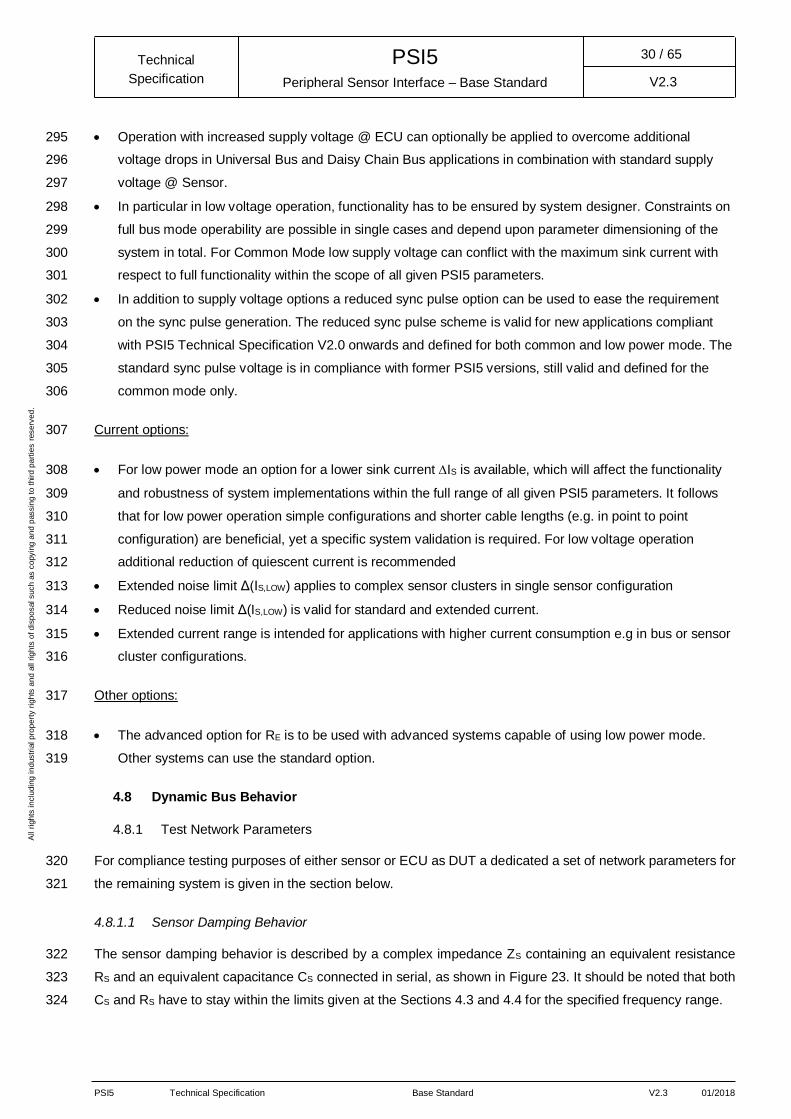
PSI5 Technical Specification Base Standard V2.3 01/2018
All r
igh
ts in
clu
din
g in
dustr
ial p
rop
ert
y r
igh
ts a
nd
all r
igh
ts o
f d
isp
osal such
as c
opyin
g a
nd
passin
g t
o t
hir
d p
art
ies
rese
rve
d.
Peripheral Sensor Interface – Base Standard
PSI5 Technical
Specification
30 / 65
V2.3
Operation with increased supply voltage @ ECU can optionally be applied to overcome additional 295
voltage drops in Universal Bus and Daisy Chain Bus applications in combination with standard supply 296
voltage @ Sensor. 297
In particular in low voltage operation, functionality has to be ensured by system designer. Constraints on 298
full bus mode operability are possible in single cases and depend upon parameter dimensioning of the 299
system in total. For Common Mode low supply voltage can conflict with the maximum sink current with 300
respect to full functionality within the scope of all given PSI5 parameters. 301
In addition to supply voltage options a reduced sync pulse option can be used to ease the requirement 302
on the sync pulse generation. The reduced sync pulse scheme is valid for new applications compliant 303
with PSI5 Technical Specification V2.0 onwards and defined for both common and low power mode. The 304
standard sync pulse voltage is in compliance with former PSI5 versions, still valid and defined for the 305
common mode only. 306
Current options: 307
For low power mode an option for a lower sink current IS is available, which will affect the functionality 308
and robustness of system implementations within the full range of all given PSI5 parameters. It follows 309
that for low power operation simple configurations and shorter cable lengths (e.g. in point to point 310
configuration) are beneficial, yet a specific system validation is required. For low voltage operation 311
additional reduction of quiescent current is recommended 312
Extended noise limit Δ(IS,LOW) applies to complex sensor clusters in single sensor configuration 313
Reduced noise limit Δ(IS,LOW) is valid for standard and extended current. 314
Extended current range is intended for applications with higher current consumption e.g in bus or sensor 315
cluster configurations. 316
Other options: 317
The advanced option for RE is to be used with advanced systems capable of using low power mode. 318
Other systems can use the standard option. 319
4.8 Dynamic Bus Behavior
4.8.1 Test Network Parameters
For compliance testing purposes of either sensor or ECU as DUT a dedicated a set of network parameters for 320
the remaining system is given in the section below. 321
4.8.1.1 Sensor Damping Behavior
The sensor damping behavior is described by a complex impedance ZS containing an equivalent resistance 322
RS and an equivalent capacitance CS connected in serial, as shown in Figure 23. It should be noted that both 323
CS and RS have to stay within the limits given at the Sections 4.3 and 4.4 for the specified frequency range. 324
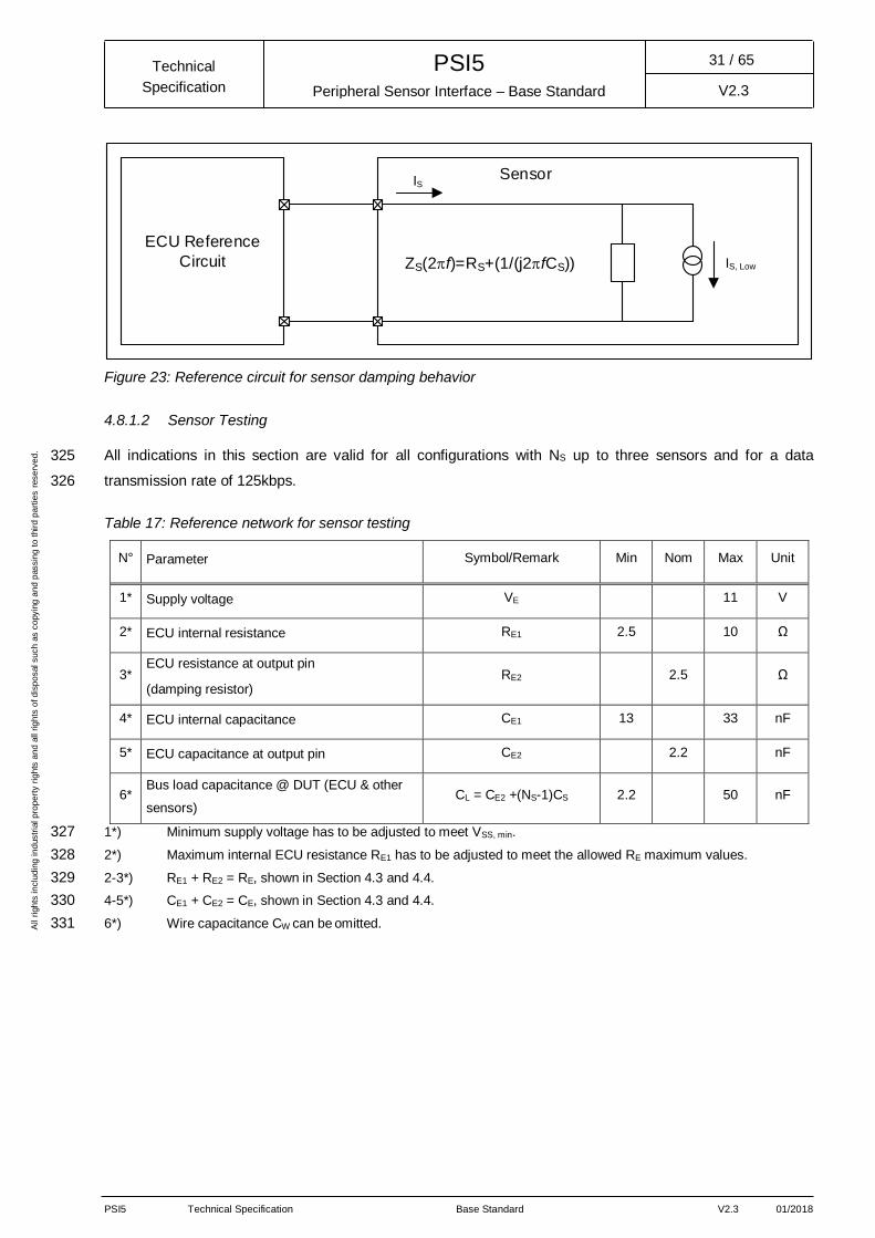
PSI5 Technical Specification Base Standard V2.3 01/2018
All r
igh
ts in
clu
din
g in
dustr
ial p
rop
ert
y r
igh
ts a
nd
all r
igh
ts o
f d
isp
osal such
as c
opyin
g a
nd
passin
g t
o t
hir
d p
art
ies
rese
rve
d.
Peripheral Sensor Interface – Base Standard
PSI5 Technical
Specification
31 / 65
V2.3
Figure 23: Reference circuit for sensor damping behavior
4.8.1.2 Sensor Testing
All indications in this section are valid for all configurations with NS up to three sensors and for a data 325
transmission rate of 125kbps. 326
Table 17: Reference network for sensor testing
N° Parameter Symbol/Remark Min Nom Max Unit
1* Supply voltage VE 11 V
2* ECU internal resistance RE1 2.5 10 Ω
3* ECU resistance at output pin
(damping resistor) RE2 2.5 Ω
4* ECU internal capacitance CE1 13 33 nF
5* ECU capacitance at output pin CE2 2.2 nF
6* Bus load capacitance @ DUT (ECU & other
sensors) CL = CE2 +(NS-1)CS 2.2 50 nF
1*) Minimum supply voltage has to be adjusted to meet VSS, min. 327
2*) Maximum internal ECU resistance RE1 has to be adjusted to meet the allowed RE maximum values. 328
2-3*) RE1 + RE2 = RE, shown in Section 4.3 and 4.4. 329
4-5*) CE1 + CE2 = CE, shown in Section 4.3 and 4.4. 330
6*) Wire capacitance CW can be omitted. 331
ZS
ECU Reference
Circuit
IS
ZS(2pf)=RS+(1/(j2pfCS)) IS, Low
Sensor

PSI5 Technical Specification Base Standard V2.3 01/2018
All r
igh
ts in
clu
din
g in
dustr
ial p
rop
ert
y r
igh
ts a
nd
all r
igh
ts o
f d
isp
osal such
as c
opyin
g a
nd
passin
g t
o t
hir
d p
art
ies
rese
rve
d.
Peripheral Sensor Interface – Base Standard
PSI5 Technical
Specification
32 / 65
V2.3
Figure 24: Reference circuit for sensor testing
4.8.1.3 ECU Testing
All indications in this section are valid for all configurations with NS up to three sensors and for a data 332
transmission rate of 125kbps. All other sensor parameters follow the values given at Sections 4.3 and 4.4. 333
Table 18: Reference network for ECU testing
N° Parameter Symbol/Remark Min Nom Max Unit
6* Bus load capacitance @ DUT (all sensors) CL = (NS)CS 2.2 50 nF
Figure 25: Reference circuit for ECU testing
4.8.2 Requirements for Dynamic Sensor Testing
In order to verify the proper sensor behavior the dynamic performance needs to be tested. To do so two test 334
scenarios are given below: A and B. These represent the inductive (A) and capacitive (B) worst case coupling 335
on a bus respectively. The fulfillment of the parameters below are a necessary requirement for compliance of 336
the sensor device to PSI5 Specification. Nevertheless it is mandatory to verify the proper communication within 337
a bus configuration in the final application. In Figure 26 and Table 19 all relevant test conditions are given. 338
Sensor
DUT
ISECU Reference Circuit
VECE1
RE1 RE2
CL
IE
VSS
RW LW
ECU
DUT
IS
IS, Low
Sensor Reference Circuit
ZS
IS, High
CL
RW LW
VSS

PSI5 Technical Specification Base Standard V2.3 01/2018
All r
igh
ts in
clu
din
g in
dustr
ial p
rop
ert
y r
igh
ts a
nd
all r
igh
ts o
f d
isp
osal such
as c
opyin
g a
nd
passin
g t
o t
hir
d p
art
ies
rese
rve
d.
Peripheral Sensor Interface – Base Standard
PSI5 Technical
Specification
33 / 65
V2.3
Figure 26: Dynamic behavior of supply / communication current
Table 19: Parameter specification for sensor reference test
N° Parameter Symbol/Remark Min Nom Max Unit
A* Worst case overshoot @ ECU
Test condition: RE1 = 2.5Ω; CE variable between 13nF and 33nF; CL = 2.2nF; RW = 0.1Ω; LW = 8.7µH
A1 Sending current over- / undershoot @ ECU IOvershoot, rise & IUndershoot, fall (IS) 50 %
A2 Time for under- / overshoot @ ECU tUndershoot, rise & tOvershoot, fall (IE) 0.52 µs
A3 Settling time @ ECU tSettle (IE) 1.72 µs
A4* Voltage ripple @ Sensor referenced to VSS, base -0.8 +0.8 V
B* Worst case timing @ ECU
Test condition: RE1 = 10Ω (7Ω); CE = 33nF; CL = 50nF; Rwire = 2.5Ω; Lwire = 0µH
B1 Sending current rise/fall time @ ECU trise 20, 80 & tfall 80, 20 (IE) 1.8 µs
A*) The sensor has to fulfill reference Test A for every value of the capacitance CE. 339
A4*) Parameter is only valid for systems in common mode operation with a minimum VCE of 5.5V (VSS=5.0V). For low 340
voltage operation the maximum allowed voltage ripple can differ, but has to be validated on system level. 341
B*) Maximum internal ECU resistance RE1 has to be adjusted to meet the allowed RE maximum values. 342
4.8.3 Requirements for Dynamic ECU Testing
In order to verify the proper ECU behavior the dynamic performance needs to be tested. To do so two test 343
scenarios are given below: A and B. These represent the inductive (A) and capacitive (B) worst case coupling 344
on a bus respectively. The fulfillment of the parameters below are a necessary requirement for compliance of 345
IOvershoot
tSettle
trise 20,80
tUndershoot
trise
20
100
80
20
trise
80
t
IE,IS [%]

PSI5 Technical Specification Base Standard V2.3 01/2018
All r
igh
ts in
clu
din
g in
dustr
ial p
rop
ert
y r
igh
ts a
nd
all r
igh
ts o
f d
isp
osal such
as c
opyin
g a
nd
passin
g t
o t
hir
d p
art
ies
rese
rve
d.
Peripheral Sensor Interface – Base Standard
PSI5 Technical
Specification
34 / 65
V2.3
the ECU to the PSI5 Specification. Nevertheless it is mandatory to verify the proper communication within a 346
bus configuration in the final application. 347
Table 20: Parameter specification for ECU reference test
N° Parameter Symbol/Remark Min Nom Max Unit
A*
Worst case overshoot @ ECU
Test condition: RE1 = 2.5Ω; CL = 2.2nF; RW = 0.1Ω; LW = 8.7µH; CS variable
between 9nF and 24nF @10 …200KHz and between 1.32nF and 24 nF @ 200KHz…2MHz;
A1* Supply Voltage @ ECU VCE,min VCE,BASE,max V
B* Worst case timing @ ECU
Test condition: RS = 10Ω; CS = 24nF; CL = 50nF; Rwire = 2.5Ω; Lwire = 0µH;
B1* Supply Voltage @ ECU VCE,min VCE,BASE,max V
A*) The sensor has to fulfill reference Test A for every value of the capacitance CS. 348
A1,B1*) For min max values see Table 14. 349
4.9 Synchronization Signal
Purpose of the synchronization signal is to provide a time base for all devices connected to the interface. The 350
synchronization signal is realized by a positive voltage modulation on the power supply lines. For ECU to 351
sensor communication, bits are encoded in present or missing sync pulses, respectively. Or optional by 352
generating long and short sync pulses. The sync pulses are defined as shown in Figure 27 and in the Table 353
21. 354

PSI5 Technical Specification Base Standard V2.3 01/2018
All r
igh
ts in
clu
din
g in
dustr
ial p
rop
ert
y r
igh
ts a
nd
all r
igh
ts o
f d
isp
osal such
as c
opyin
g a
nd
passin
g t
o t
hir
d p
art
ies
rese
rve
d.
Peripheral Sensor Interface – Base Standard
PSI5 Technical
Specification
35 / 65
V2.3
Figure 27: Shape and timing of synchronization signal at ECU
The synchronization signal start time t0 is defined as a crossing of the Vt0 value. In the “Sync Start” phase 355
before this point, a “rounding in” of the voltage starting from VCE, Base to Vt0 is allowed for a maximum of t1. 356
During the “Sync Slope” phase, the voltage rises within given slew rates to a value between the minimum sync 357
signal voltage Vt2 and the maximum interface voltage VCE, max / VSS, max. After maintaining between these limits 358
until a minimum of t03 (t13), the voltage decreases in the “Sync Discharge” phase until having reached the initial 359
VCE, base value until latest t04. (t14) 360
Table 21: Parameter specification of synchronization signal
N° Parameter Symbol Conditions/Remark Min Nom Max Unit
1* Sync slope reference voltage Vt0 Referenced to VCE, BASE (0.5) V
2*
Sync signal sustain voltage Vt2
Reduced sync pulse;
Referenced to VCE, BASE 2.5
V
3* Standard sync pulse;
Referenced to VCE, BASE 3.5
4* Reference time t0 Reference time base (0) µs
5 Sync signal earliest start t1 Delta current less than 2mA -3 µs
6 Sync signal sustain start t2 @ Vt2 7 µs
7* Sync slope rising slew rate VSync, SR,
rise 0.43 1.5 V/µs
Lower Boundary
Trigger
Point
Phase 1 SyncStart
Phase 2 Sync Slope
Phase 3 Sync
Sustain
Phase 4 Sync
DischargeVCE, max /
VSS, max
Vt2
VTRIG
Vt0
t1 t0 tTRIG t2 t03 t
04 t
13 t
14
VCE Base
Short sync pulse [0]
Long sync pulse [1]
t
PSI5 Technical Specification Base Standard V2.3 01/2018
All r
igh
ts in
clu
din
g in
dustr
ial p
rop
ert
y r
igh
ts a
nd
all r
igh
ts o
f d
isp
osal such
as c
opyin
g a
nd
passin
g t
o t
hir
d p
art
ies
rese
rve
d.
Peripheral Sensor Interface – Base Standard
PSI5 Technical
Specification
36 / 65
V2.3
N° Parameter Symbol Conditions/Remark Min Nom Max Unit
8 Sync slope falling slew rate VSync, SR,
fall -1.5 V/µs
9 Sync signal sustain time
t03 16 µs
t13 43
10* Discharge time limit
t04 35 µs
t14 62
11
Start of first sensor data word tSlot 1 Start
Tooth gap method 44 µs
12 Pulse width method 71 µs
1,4*) Theoretical value 361
2*) The reduced sync pulse scheme is valid for new applications compliant with PSI5 Technical Specification V2.0 362
onwards. However, in compliance with former PSI5 versions the standard sync pulse scheme is still valid. 363
2,3*) Vt2, max is subject to application specific definitions and limited by absolute maximum ratings to (VCE, max - VCE, 364
BASE). 365
7*) Lower limit is valid for rising slew rate Vt0 to Vt2 366
10*) Common Mode: Remaining discharge current <2 mA, to be guaranteed by the ECU; 367
Low Power Mode: With Low Power Mode sink current ∆IS a remaining discharge current <0.4 mA has to be 368
guaranteed by the ECU 369
In the sensors, the trigger is detected within the “trigger window” during the rising slope of the synchronization 370
signal at the trigger point with the trigger voltage VTRIG and the trigger time tTRIG. 371

PSI5 Technical Specification Base Standard V2.3 01/2018
All r
igh
ts in
clu
din
g in
dustr
ial p
rop
ert
y r
igh
ts a
nd
all r
igh
ts o
f d
isp
osal such
as c
opyin
g a
nd
passin
g t
o t
hir
d p
art
ies
rese
rve
d.
Peripheral Sensor Interface – Base Standard
PSI5 Technical
Specification
37 / 65
V2.3
Figure 28: Synchronization signal detection in the sensor
In order to take into account voltage differences at different points of the interface lines, an additional safety 372
margin for the trigger detection is defined by VEMC and tEMC. 373
Table 22: Parameter specification of synchronization signal detection at the sensor
N° Parameter Symbol Conditions/Remark Min Nom Max Unit
1 Margin for voltage variations of
the signal on the interface line
due to EMC effects
VEMC
Reduced sync pulse -0.7 +0.7 V
2 Standard sync pulse -0.9 +0.9
3*
Sensor trigger threshold VTRIG
Reduced sync pulse;
Sensor to detect trigger 1.2 1.5 1.8 V
4* Standard sync pulse;
Sensor to detect trigger 1.4 2.0 2.6 V
5* Nominal trigger detection time tTRIG @ VTRIG , @ Sensor Pins (2.1) (3.5) (4.9) µs
6 Variation time of the signal on
the interface line due to EMC TEMC
Relative to nominal trigger
window time -2.1 +2.1 µs
7
Tolerance time of internal
trigger detection delay at
sensor
Ttol detect 3 µs
t
TEMC
VEMC
TEMC
VEMC
Sync Slope Window
Trigger Window
Trigger Point
t0t1 TTRIG
min
TTRIG
nom
TTRIG
max
t2
Vt2
VTRIG max
VTRIG
VTRIG min
Vt0
VSS Base

PSI5 Technical Specification Base Standard V2.3 01/2018
All r
igh
ts in
clu
din
g in
dustr
ial p
rop
ert
y r
igh
ts a
nd
all r
igh
ts o
f d
isp
osal such
as c
opyin
g a
nd
passin
g t
o t
hir
d p
art
ies
rese
rve
d.
Peripheral Sensor Interface – Base Standard
PSI5 Technical
Specification
38 / 65
V2.3
N° Parameter Symbol Conditions/Remark Min Nom Max Unit
8* Trigger detection window TTRIG TTRIG = tTRIG,max +Ttol detect +TEMC
Reference for sensor timebase 0 10 µs
3-4*) Referenced to VSS, BASE. 374
5*) Referenced to a straight sync signal slope with nominal slew rate. Values in brackets are for illustration purposes 375
only 376
8*) Additional fixed internal delays are possible but have to be considered for the data slot time calculation 377
4.10 Timing Definitions for Synchronous Operation Modes
This section describes how the timing of a sensor configuration has to be calculated considering all tolerances. 378
Each single implementation has to assure that sensor frames and sync pulse do not overlap or conflict. For 379
different applications different timing considerations are of importance and hence, a transceiver should not rely 380
on concrete time slots but rather be individually configurable for different time slots. In general, timing 381
calculation is done for independent sensors at each slot. If more than one slot is used by the same sensor, or 382
two sensors rely on the same timing base, respectively, slot tolerances can be considered as dependent and 383
the timing can be tightened1). 384
State of the art operation modes and timings are specified within the effective application specific Substandard. 385
1) E.g. Substandard Chassis and Safety, Operation Mode PSI5-P20CRC-500/2L

PSI5 Technical Specification Base Standard V2.3 01/2018
All r
igh
ts in
clu
din
g in
dustr
ial p
rop
ert
y r
igh
ts a
nd
all r
igh
ts o
f d
isp
osal such
as c
opyin
g a
nd
passin
g t
o t
hir
d p
art
ies
rese
rve
d.
Peripheral Sensor Interface – Base Standard
PSI5 Technical
Specification
39 / 65
V2.3
4.10.1 Generic Time Slot Calculation
Figure 29: Timing of synchronous operation
tnES : Earliest start of frame, slot n; this is the earliest time when the transceiver or any other sensor on 386
the bus can expect that the frame no. n begins. 387
tnNS : Nominal start of frame, slot n; this is the nominal time when the sender (sensor) transmits data 388
according to its own internal clock. It is the nominal time when the transceiver or any other sensor 389
on the bus can expect that the frame no. n begins. 390
tnNS, prog : nominal start value of frame, slot n, that is programmed to the sensor. It is derived from tnNS by 391
rounding up to the next discretization value. 392
tnLS : Latest start of frame, slot n; this is the latest time when the transceiver or any other sensor on the 393
bus can expect that the frame no. n begins. 394
tnEE : Earliest end of frame, slot n; this is the earliest time when the transceiver or any other sensor on 395
the bus can expect that the frame no. n is over. 396
tnNE : Nominal end of frame, slot n. 397
tnLE : Latest end of frame, slot n; this is the latest time when the transceiver or any other sensor on the 398
bus can expect that the frame no. n is over. 399
TGAP: Minimum gap time which must be guaranteed between two frames (see Table 13) 400
TTRIG: Trigger detection window to detect the sync pulse = tTRIG,max + Ttol detect + TEMC (see Table 22) 401
TSync: Duration of sync period e.g. for 1% transceiver clock tolerance: TSync, min = TSync*0.99; TSync, max = 402
TSync*1.01 403
tSlot 1 Start: Earliest Start of first sensor data word (see Table 22) 404
TBIT: Nominal time for a single bit (see Table 13) 405
t1 : Sync signal earliest start (see Table 21) 406
Mn: No. of bits including start, data and parity or crc bits for frame, slot n. 407
N: No. of time slots within one sync cycle 408
TSync
TGAP
tnES
tnNS t
nLS
tnEE
tnLE
tnNS
tSlot N, End
tnNE t
nNEt0
TTRIG TTRIG
VSS Base
TSlot1

PSI5 Technical Specification Base Standard V2.3 01/2018
All r
igh
ts in
clu
din
g in
dustr
ial p
rop
ert
y r
igh
ts a
nd
all r
igh
ts o
f d
isp
osal such
as c
opyin
g a
nd
passin
g t
o t
hir
d p
art
ies
rese
rve
d.
Peripheral Sensor Interface – Base Standard
PSI5 Technical
Specification
40 / 65
V2.3
CTn: Clock tolerance of the transmitter (sensor) sending the frame no. n. 409
For n=1 410
t1ES = tSlot 1 Start +TTRIG, min 411
t1NS 2*) ≥ tSlot 1 Start /(1-CT1) 412
t1LS ≥ t1NS, prog *(1+CT1)+TTRIG, max 413
t1EE ≥ t1ES+M1*TBIT*(1-CT1) 414
t1LE : ≥ t1LS+M1*TBIT*(1+CT1) 415
For n=2…N 416
tnES ≥ (tn-1LE+TGAP)+TTRIG, min 417
tnNS *) ≥ (tn-1LE+TGAP)/(1-CTn) 418
tnLS ≥ tnNS, prog *(1+CT1)+TTRIG, max 419
tnEE ≥ tnES+Mn*TBIT*(1-CTn) 420
tnLE ≥ tnLS+Mn*TBIT*(1+CTn) 421
The last frame must end before the next sync pulse starts. For secure data reception a final TGAP should be 422
considered3): 423
tSlot N, End = tNLE (+ TGAP) < TSync, min + t1 424
Note: 425
“≥” is used since the final frame timing should be equalized in order to cover the whole sync period with 426
maximum margins. 427
Transceiver clock tolerance determines effective sync pulse duration. A clock tolerance of 1% is 428
assumed. (see also TSYNC) 429
A discretization of the calculated timings of nominal 0.5us is proposed 430
Please refer to each Substandard for details on timing specification and typical operation modes. 431
2) The nominal trigger detection tolerance is neglected for calculation of tnNS since the nominal start time
typically is used for sensor programming where detection tolerances do not apply. For the same reason it is
recommended to round up tnNS to 0.5µs and use the rounded value (tnNS, prog) for the calculation of the latest
start time tnLS
3) Exceptional definitions omitting final TGAP are possible.

PSI5 Technical Specification Base Standard V2.3 01/2018
All r
igh
ts in
clu
din
g in
dustr
ial p
rop
ert
y r
igh
ts a
nd
all r
igh
ts o
f d
isp
osal such
as c
opyin
g a
nd
passin
g t
o t
hir
d p
art
ies
rese
rve
d.
Peripheral Sensor Interface – Base Standard
PSI5 Technical
Specification
41 / 65
V2.3
4.11 Sensor Power-on Characteristics
To ensure a proper startup of the system, a maximum startup time tSET1 is specified. During this time, the ECU 432
must provide a minimum current to load capacitances in sensors and wires. After this, the sensor must sink to 433
quiescent current within the specified tolerance band. 434
During power on the ECU may reduce the output voltage to limit the current. However, this situation must be 435
avoided in case of the daisy chain bus. Therefore, in a Daisy Chain Bus the sensor architecture must ensure 436
that the overall bus current stays below ILIMIT, dyn.. 437
4.11.1 Sensor Bus Configuration
Figure 30: Current consumption during startup for sensor bus configuration
Table 23: Settling time specification for sensor bus configuration
N° Parameter Symbol Conditions/Remark Min Typ Max Unit
1*
Settling time for quiescent current ILOW tSET1 inrush current limitation 5.0 ms
2* Daisy Chain Bus 10.0 ms
1*) Final value settles to ILOW with the defined signal noise limits ΔILow (see Table 14). 438
2*) Mandatory settling time for quiescent current in Daisy Chain Bus. The Bus does not sink a current over ILIMIT,dyn. 439
at any time. 440
I
t
Sensor current consumption
Signal noise limit ΔILOW
Steady state quiescent current
tSET1
ILIMIT
ILOW
0
0
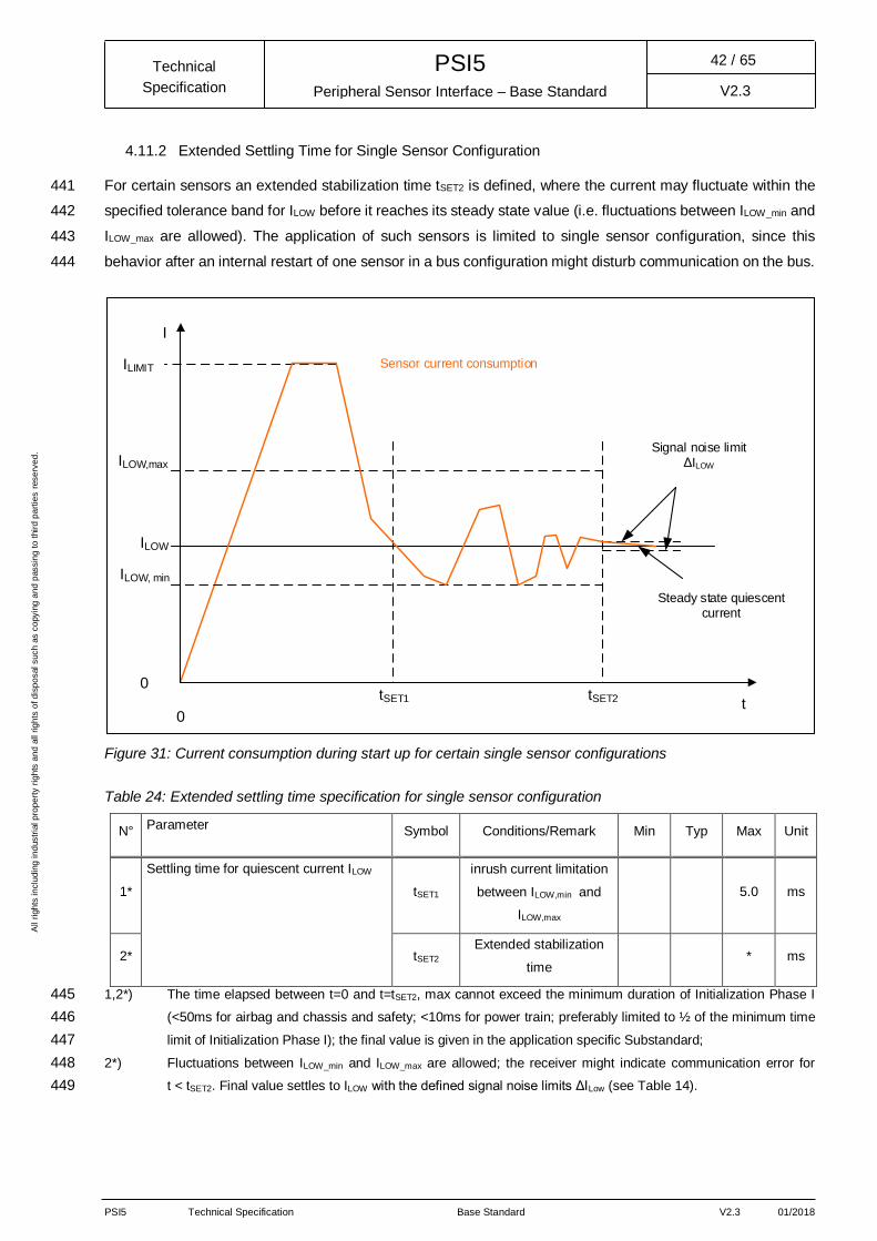
PSI5 Technical Specification Base Standard V2.3 01/2018
All r
igh
ts in
clu
din
g in
dustr
ial p
rop
ert
y r
igh
ts a
nd
all r
igh
ts o
f d
isp
osal such
as c
opyin
g a
nd
passin
g t
o t
hir
d p
art
ies
rese
rve
d.
Peripheral Sensor Interface – Base Standard
PSI5 Technical
Specification
42 / 65
V2.3
4.11.2 Extended Settling Time for Single Sensor Configuration
For certain sensors an extended stabilization time tSET2 is defined, where the current may fluctuate within the 441
specified tolerance band for ILOW before it reaches its steady state value (i.e. fluctuations between ILOW_min and 442
ILOW_max are allowed). The application of such sensors is limited to single sensor configuration, since this 443
behavior after an internal restart of one sensor in a bus configuration might disturb communication on the bus. 444
Figure 31: Current consumption during start up for certain single sensor configurations
Table 24: Extended settling time specification for single sensor configuration
N° Parameter
Symbol Conditions/Remark Min Typ Max Unit
1*
Settling time for quiescent current ILOW
tSET1
inrush current limitation
between ILOW,min and
ILOW,max
5.0 ms
2* tSET2 Extended stabilization
time * ms
1,2*) The time elapsed between t=0 and t=tSET2, max cannot exceed the minimum duration of Initialization Phase I 445
(<50ms for airbag and chassis and safety; <10ms for power train; preferably limited to ½ of the minimum time 446
limit of Initialization Phase I); the final value is given in the application specific Substandard; 447
2*) Fluctuations between ILOW_min and ILOW_max are allowed; the receiver might indicate communication error for 448
t < tSET2. Final value settles to ILOW with the defined signal noise limits ΔILow (see Table 14). 449
Sensor current consumption
Signal noise limit ΔILOW
Steady state quiescent current
tSET1
ILIMIT
ILOW
0
0
tSET2
ILOW,max
ILOW, min
t
I
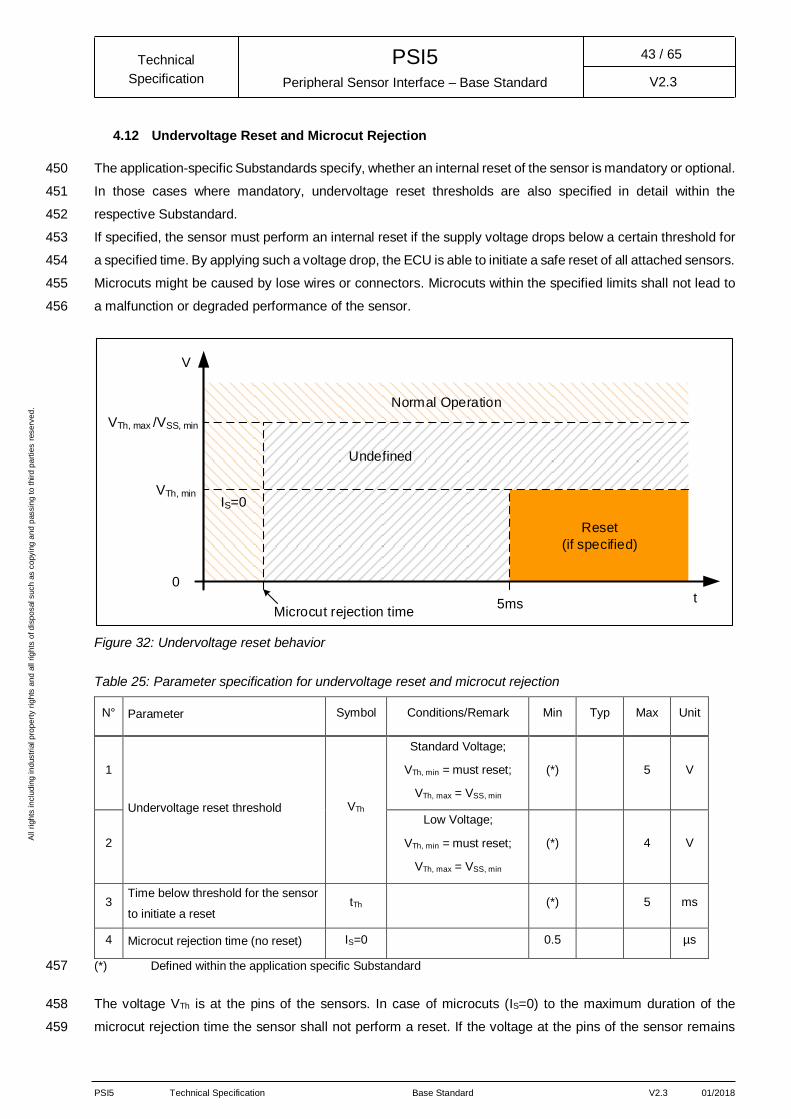
PSI5 Technical Specification Base Standard V2.3 01/2018
All r
igh
ts in
clu
din
g in
dustr
ial p
rop
ert
y r
igh
ts a
nd
all r
igh
ts o
f d
isp
osal such
as c
opyin
g a
nd
passin
g t
o t
hir
d p
art
ies
rese
rve
d.
Peripheral Sensor Interface – Base Standard
PSI5 Technical
Specification
43 / 65
V2.3
4.12 Undervoltage Reset and Microcut Rejection
The application-specific Substandards specify, whether an internal reset of the sensor is mandatory or optional. 450
In those cases where mandatory, undervoltage reset thresholds are also specified in detail within the 451
respective Substandard. 452
If specified, the sensor must perform an internal reset if the supply voltage drops below a certain threshold for 453
a specified time. By applying such a voltage drop, the ECU is able to initiate a safe reset of all attached sensors. 454
Microcuts might be caused by lose wires or connectors. Microcuts within the specified limits shall not lead to 455
a malfunction or degraded performance of the sensor. 456
Figure 32: Undervoltage reset behavior
Table 25: Parameter specification for undervoltage reset and microcut rejection
N° Parameter Symbol Conditions/Remark Min Typ Max Unit
1
Undervoltage reset threshold VTh
Standard Voltage;
VTh, min = must reset;
VTh, max = VSS, min
(*) 5 V
2
Low Voltage;
VTh, min = must reset;
VTh, max = VSS, min
(*) 4 V
3 Time below threshold for the sensor
to initiate a reset tTh (*) 5 ms
4 Microcut rejection time (no reset) IS=0 0.5 µs
(*) Defined within the application specific Substandard 457
The voltage VTh is at the pins of the sensors. In case of microcuts (IS=0) to the maximum duration of the 458
microcut rejection time the sensor shall not perform a reset. If the voltage at the pins of the sensor remains 459
VTh, max /VSS, min
Reset
(if specified)
IS=0
Normal Operation
t
Undefined
5msMicrocut rejection time
VTh, min
0
V

PSI5 Technical Specification Base Standard V2.3 01/2018
All r
igh
ts in
clu
din
g in
dustr
ial p
rop
ert
y r
igh
ts a
nd
all r
igh
ts o
f d
isp
osal such
as c
opyin
g a
nd
passin
g t
o t
hir
d p
art
ies
rese
rve
d.
Peripheral Sensor Interface – Base Standard
PSI5 Technical
Specification
44 / 65
V2.3
above VTh,max the sensor must not perform a reset. If the voltage at the pins of the sensor falls below VTh, min 460
for more than 5ms the sensor has to perform a reset, if a reset is specified in the application specific 461
Substandard. 462
Different definitions may apply for Universal Bus and Daisy Chain Bus. 463

PSI5 Technical Specification Base Standard V2.3 01/2018
All r
igh
ts in
clu
din
g in
dustr
ial p
rop
ert
y r
igh
ts a
nd
all r
igh
ts o
f d
isp
osal such
as c
opyin
g a
nd
passin
g t
o t
hir
d p
art
ies
rese
rve
d.
Peripheral Sensor Interface – Base Standard
PSI5 Technical
Specification
45 / 65
V2.3
5 Application Layer
Specific application layer implementations are defined in the application Substandards or in individual product 464
specifications. In order to enable global interoperability between PSI5 compatible components and to avoid 465
potential system malfunction due to erroneous recognition of components, some global definitions about data 466
range, sensor initialization and bidirectional communication are made in this section. 467
5.1 Data Range
PSI5 data messages, transmitted in data region A, are divided into three separate ranges: a data range for the 468
sensor output signal, a range for status and error messages and a range for initialization data. 469
For 10 bit sensors, the decimal values –480 to +480 are used for the sensor output signal. The range –512 to 470
–481 is reserved for the block and data ID’s and can be used for transmitting initialization data during startup 471
of the sensor (see Chapter 5.2). The range from +481 to +511 is used for status and error messages. 472
Table 26: Data range (10 Bit)
value
Signification Range
Dec Hex
+511 0x1FF Reserved (ECU internal use) 1)
Status & Error
Messages 2
: : Reserved (ECU internal use) 1)
+504 0x1F8 Reserved (ECU internal use) 1)
+503 0x1F7 Reserved (Sensor use) 2)
+502 0x1F6 Reserved (Sensor use) 2)
+501 0x1F5 Reserved (Sensor use) 2)
+500 0x1F4 “Sensor Defect”
+499 0x1F3 Reserved (ECU internal use) 1)
: : Reserved (ECU internal use) 1)
+496 0x1F0 Reserved (ECU internal use) 1)
+495 0x1EF Reserved (Sensor use) 2)
: : Reserved (Sensor use) 2)
+489 0x1E9 “Sensor in Service Mode”
+488 0x1E8 “Sensor Busy”
+487 0x1E7 “Sensor Ready”
+486 0x1E6 “Sensor Ready but Unlocked”
+485 0x1E5 Reserved (Sensor use) 2)
+484 0x1E4 Reserved (Sensor use) 2)
+483 0x1E3 Reserved (Sensor use) 2)
+482 0x1E2 Bidirectional Communication: RC “Error”
+481 0x1E1 Bidirectional Communication: RC “O.K.”

PSI5 Technical Specification Base Standard V2.3 01/2018
All r
igh
ts in
clu
din
g in
dustr
ial p
rop
ert
y r
igh
ts a
nd
all r
igh
ts o
f d
isp
osal such
as c
opyin
g a
nd
passin
g t
o t
hir
d p
art
ies
rese
rve
d.
Peripheral Sensor Interface – Base Standard
PSI5 Technical
Specification
46 / 65
V2.3
value
Signification Range
Dec Hex
+480 0x1E0 Maximum Sensor Data value
Sensor Output Signal 1
: : :
0 0x000
: : :
-480 0x220 Minimum Sensor Data value
-481 0x21F Status Data 1111
Data for Initialization
3
: : :
-496 0x210 Status Data 0000
-497 0x20F Block ID 16
Block ID's : : :
-512 0x200 Block ID 1
1) Usage for ECU internal purpose possible (e.g. “No Data”, “Manchester Error” etc.) 473
2) Reserved for application specific definitions. Detailed description is given within the application specific 474
Substandard. 475
5.1.1 Scaling of Sensor Output
For sensors with a data word length of more than 10 bit, the data range scales as described in Chapter 3.1.3. 476
In this case status and initialization data words of range 2 and 3 are filled up with a value to be defined in the 477
application specific substandard. 478
Figure 33: Mapping of status and initialization data into a data word
5.2 Sensor Initialization / Identification
Sensor Initialization data is sent after each power on or reset. Therefore two different transmission procedures 479
can be applied: 480
D15 D14 D13 D12 D11 D10 D9 D8 D7 D6 D5 D4 D3 D2 D1 D0
D9 D8 D7 D6 D5 D4 D3 D2 D1 D0
1 11110 0 0 0 0
1 11110 0 0 0 0 X X X X X X
„2“ „0“ „F“
16 BitData Word
10 BitData Word
Example„Block ID 16"0x20F
Mapping of Status & Initialization Data

PSI5 Technical Specification Base Standard V2.3 01/2018
All r
igh
ts in
clu
din
g in
dustr
ial p
rop
ert
y r
igh
ts a
nd
all r
igh
ts o
f d
isp
osal such
as c
opyin
g a
nd
passin
g t
o t
hir
d p
art
ies
rese
rve
d.
Peripheral Sensor Interface – Base Standard
PSI5 Technical
Specification
47 / 65
V2.3
1) Data Range Initialization: Identification data is sent during an initialization procedure before any 481
effective sensor data is sent. 482
2) Serial Channel Messaging: For immediate access to measurement data, identification data is 483
transmitted parallel to sensor data via serial channel bits M0 and M1. The sensor immediately starts 484
with parallel transmission of measurement and sensor identification data. 485
Figure 34: Sensor initialization sequence for Data Range Initialization
Chapter 5.2.1 defines the Data format of the Data Range Initialization procedure, further details are given in 486
the corresponding Substandards. The Serial Channel Messaging is fully defined on application level, i.e. within 487
the specific Substandard. Chapter 5.2.2 and 5.2.3 define basic regulations of the Application Layer that need 488
to be followed by both identification procedures. 489
5.2.1 Frame Format - Data Range Initialization
The initialization data is transmitted within the range of “Payload Data Region A” out of the reserved data range 490
2 and 3 in Table 26. Sensor identification data is sent via data range 3 using ID and data blocks containing 491
each 16 block identifiers and 4-bit data nibbles. Exceptions or failure modes are sent via data range 2. 492
Initialization Phase
I
Start-up
No data
transmission
Initialization Phase
II
Data content
Transmission of
type code
& serial N°
Sensor self test
Initialization Phase
III
Status
Transmission of
„Sensor ready“,
„Sensor defect“,
or other sensor
specific data
Run Mode
Transmission of
sensor or
status data
Start-up and
Initialization
ID1 D1 ID1 D1 ID1 D1 ID2 D2
t = 0 tINT1 tINT2 tINT3
Transmission of
initialization data
k * (Idn + Dn)

PSI5 Technical Specification Base Standard V2.3 01/2018
All r
igh
ts in
clu
din
g in
dustr
ial p
rop
ert
y r
igh
ts a
nd
all r
igh
ts o
f d
isp
osal such
as c
opyin
g a
nd
passin
g t
o t
hir
d p
art
ies
rese
rve
d.
Peripheral Sensor Interface – Base Standard
PSI5 Technical
Specification
48 / 65
V2.3
Figure 35: Block ID and data nibbles
ID blocks and data blocks are sent in an alternating sequence. 493
Figure 36: Startup sequence
If the initialization data exceeds 4x16=64 bit, data can be “paged”. The ID codes are reused for every 64 bit 494
page of data to be transmitted. Data pages are not numbered. Mapping of the information contained in different 495
data pages has to be derived from the chronology of the startup sequence. It is not mandatory to transmit 496
complete data pages. 497
5.2.2 Data Content - Data Range Initialization
Table 27: Mandatory definitions
A9 A8 A7 A6 A5 A4 A3 A2 A1 A0
1 0 0 0 0 0 0000-1111
Block ID 1-16
(0x200 – 0x20F)
A9 A8 A7 A6 A5 A4 A3 A2 A1 A0
1 0 0 0 0 0 0000-1111
Data Nibbles
„0000" – „1111"
(0x210 – 0x21F)
Block Identifier and Data Nibbles
Initialization ID1 D1 ID2 D2 ID3 D3 ... ...
Hex Value 0x200 0x214 0x201 0x211 0x202 0x21B
Data Content 0100 0001 1011
ID1 D1 ... ID1 D1 ID2 D2 ... ID2 D2
Initialization Data Transmission
Initialization Sequence Example (k=1)
D1 = 0100 (PSI5 Protocol Revision)
D2 = 0001 (Example for number ofD3 = 1011 data nibbles = 27 dec)
Repetition of ID and data blocks(optional)
k * (Idn + Dn)
Header Initialization Vendor ID Product ID
Data field F1 F2 F3 F4 F5
Data nibble D1 D2 D3 D4 D5 D6 D7 D8 D9
PSI5 version No. of data nibbles Vendor ID Sensor type Sensor parameters
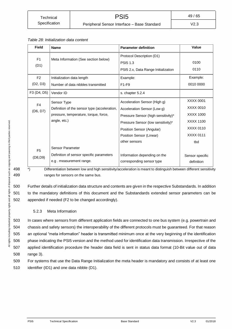
PSI5 Technical Specification Base Standard V2.3 01/2018
All r
igh
ts in
clu
din
g in
dustr
ial p
rop
ert
y r
igh
ts a
nd
all r
igh
ts o
f d
isp
osal such
as c
opyin
g a
nd
passin
g t
o t
hir
d p
art
ies
rese
rve
d.
Peripheral Sensor Interface – Base Standard
PSI5 Technical
Specification
49 / 65
V2.3
Table 28: Initialization data content
*) Differentiation between low and high sensitivity/acceleration is meant to distinguish between different sensitivity 498
ranges for sensors on the same bus. 499
Further details of initialization data structure and contents are given in the respective Substandards. In addition 500
to the mandatory definitions of this document and the Substandards extended sensor parameters can be 501
appended if needed (F2 to be changed accordingly). 502
5.2.3 Meta Information
In cases where sensors from different application fields are connected to one bus system (e.g. powertrain and 503
chassis and safety sensors) the interoperability of the different protocols must be guaranteed. For that reason 504
an optional “meta information” header is transmitted minimum once at the very beginning of the identification 505
phase indicating the PSI5 version and the method used for identification data transmission. Irrespective of the 506
applied identification procedure the header data field is sent in status data format (10-Bit value out of data 507
range 3). 508
For systems that use the Data Range Initialization the meta header is mandatory and consists of at least one 509
identifier (ID1) and one data nibble (D1). 510
Field Name Parameter definition Value
F1
(D1)
Meta Information (See section below)
Protocol Description (D1)
PSI5 1.3
PSI5 2.x, Data Range Initialization
0100
0110
F2
(D2, D3)
Initialization data length
Number of data nibbles transmitted
Example:
F1-F9
Example:
0010 0000
F3 (D4, D5) Vendor ID s. chapter 5.2.4
F4
(D6, D7)
F5
(D8,D9)
Sensor Type
Definition of the sensor type (acceleration,
pressure, temperature, torque, force,
angle, etc.)
Sensor Parameter
Definition of sensor specific parameters
e.g . measurement range.
Acceleration Sensor (High g)
Acceleration Sensor (Low g)
Pressure Sensor (high sensitivity)*
Pressure Sensor (low sensitivity)*
Position Sensor (Angular)
Position Sensor (Linear)
other sensors
Information depending on the
corresponding sensor type
XXXX 0001
XXXX 0010
XXXX 1000
XXXX 1100
XXXX 0110
XXXX 0111
tbd
Sensor specific
definition

PSI5 Technical Specification Base Standard V2.3 01/2018
All r
igh
ts in
clu
din
g in
dustr
ial p
rop
ert
y r
igh
ts a
nd
all r
igh
ts o
f d
isp
osal such
as c
opyin
g a
nd
passin
g t
o t
hir
d p
art
ies
rese
rve
d.
Peripheral Sensor Interface – Base Standard
PSI5 Technical
Specification
50 / 65
V2.3
Table 29: Meta Header
Name Parameter definition Value
Header
Protocol Description (D1)
PSI5 1.x
PSI5 2.x, Data Range Initialization
PSI5 2.x, Serial Channel Initialization
0100
0110
0111
5.2.4 Vendor ID
The Vendor ID is sent with both methods and coded as defined below. 511
Table 30: Vendor IDs
*) These vendor IDs are effective from PSI5 Technical Specification V2.0 onwards and mandatory for all future 512
applications; in compliance with PSI5 V1.3 former codes are still valid. That is specifically regarding Autoliv 513
(0100 0000), Bosch (0001 0000), Continental (1000 0000), Siemens VDO (0010 0000). 514
Name Parameter definition ASCII Code
Vendor ID
(8 bit Sensor Manufacturer Code)
AB Elektronik 1100 0000
AMS 1110 0000
Analog Devices 0110 0001
Autoliv* 0100 0001
Bosch* 0100 0010
Continental* 0100 0011
Denso 0100 0100
ELMOS 0100 0101
Hella 0100 1000
IHR 0110 1001
Infineon 0100 1001
Hyundai Mobis 0100 1101
TDK 0110 1101
NXP 0100 0110
OnSemi 0100 1111
Seskion 0111 0011
ST Microelectronics 0101 0011
TRW 0101 0100
Other sensor manufacturers tbd

PSI5 Technical Specification Base Standard V2.3 01/2018
All r
igh
ts in
clu
din
g in
dustr
ial p
rop
ert
y r
igh
ts a
nd
all r
igh
ts o
f d
isp
osal such
as c
opyin
g a
nd
passin
g t
o t
hir
d p
art
ies
rese
rve
d.
Peripheral Sensor Interface – Base Standard
PSI5 Technical
Specification
51 / 65
V2.3
5.3 Bidirectional Communication
In the table below the allowed up- and downstream combinations are shown. 515
Table 31: Combination of bidirectional communication options
In the following basic regulations of data contents are given that need to be followed by all PSI5 applications. 516
5.3.1 Sensor Addresses
Table 32: Sensor addresses
Mnemonic SAdr
Signification A2 A1 A0
S0 0 0 0 Address of an unprogrammed sensor (Daisy Chain)
S1 0 0 1 Sensor 1 (Slot #1)
S2 0 1 0 Sensor 2 (Slot #2)
S3 0 1 1 Sensor 3 (Slot #3)
S4 1 0 0 Sensor 4 (Slot #4)
S5 1 0 1 Sensor 5 (Slot #5)
S6 1 1 0 Sensor 6 (Slot #6)
BCast 1 1 1 Broadcast address for all sensors
Upstream
(Sensor response to ECU)
Downstream
(ECU to Sensor) Remark
Data range 2 & 3
Tooth Gap method
note: frame format is restricted to frame 1-
3 (see Chapter 5.3.1)
PSI5 1.3 compliant
Data range 2 & 3 Pulse Width method
Serial channel Pulse Width Method

PSI5 Technical Specification Base Standard V2.3 01/2018
All r
igh
ts in
clu
din
g in
dustr
ial p
rop
ert
y r
igh
ts a
nd
all r
igh
ts o
f d
isp
osal such
as c
opyin
g a
nd
passin
g t
o t
hir
d p
art
ies
rese
rve
d.
Peripheral Sensor Interface – Base Standard
PSI5 Technical
Specification
52 / 65
V2.3
5.3.2 Function Codes and Responses for Bidirectional Communication – Frame 1 to 3
Table 33: Function codes and responses for bidirectional communication – Frame 1 to 3
*) Nibble (4 Bit) or Byte (8 Bit) instruction depending on device internal memory organization. 517
**) In case of Nibble (4 Bit) transmission Data_Hi has to be zero. 518
5.3.3 Returned Error Codes – Sensor Response for Frame 1-3
Table 34: Returned error codes – Sensor response for Frame 1-3
Err N° Mnemonic Description
0000 General General Error*
0001 Framing Framing Error
0010 CRC CRC Checksum Error
0011 Address Sensor Address not supported
Mnemonic SAdr FC Signification Response
A2 A1 A0 F2 F1 F0 o.K. Error
Set Sensor Address & Run Command (Short Data Frame)
Condition: SAdr = “000” or SAdr = “111”
SetAdr 0 0 0
Address to be
programmed
Set Sensor Address & Close Bus
Switch (The “FC” field
contains the sensor address)
RC: “o.K.”
RD1: “Address”
RC: “Error”
RD1: “ErrN°” A2 A1 A0
Run 1 1 1 0 0 0 Sensors to enter “Run Mode”
(Broadcast Message to all sensors)
RC: “o.K.”
RD1: “0000”
RC: “Error”
RD1: “ErrN°”
Execute device specific function (Short Data Frame)
Condition: SAdr = “001” to “110” and F2=”1”
Exec 1
Sensor
Address
001 .. 110
1 0 0 Execute Specific Function #1
RC: “o.K.”
RD1: Specific
RC: “Error”
RD1: “ErrN°”
Exec 2 1 0 1 Execute Specific Function #2
Exec 3 1 1 0 Execute Specific Function #3
Exec 4 1 1 1 Execute Specific Function #4
Read / Write Command (Long Data Frame)
Condition: F2=”0” and F1=”1”
RD_L Sensor
Address
001 .. 110
0 1 0 Read nibble or byte from sensor* RC: “o.K.”
RD1: Data_Lo
RD2: Data_Hi**
RC: “Error”
RD1: “ErrN°”
RD2: “0000” WR_L 0 1 1 Write nibble or byte to sensor*
Read / Write Command (XLong Data Frame)
Condition: F2=”0” and F1=”0”
RD_X Sensor
Address
0 0 0 Read data byte from sensor RC: “o.K.”
RD1,RD2: Data
RC: “Error”
RD1: “ErrN°”
RD2: “0000” WR_X 0 0 1 Write data byte to sensor
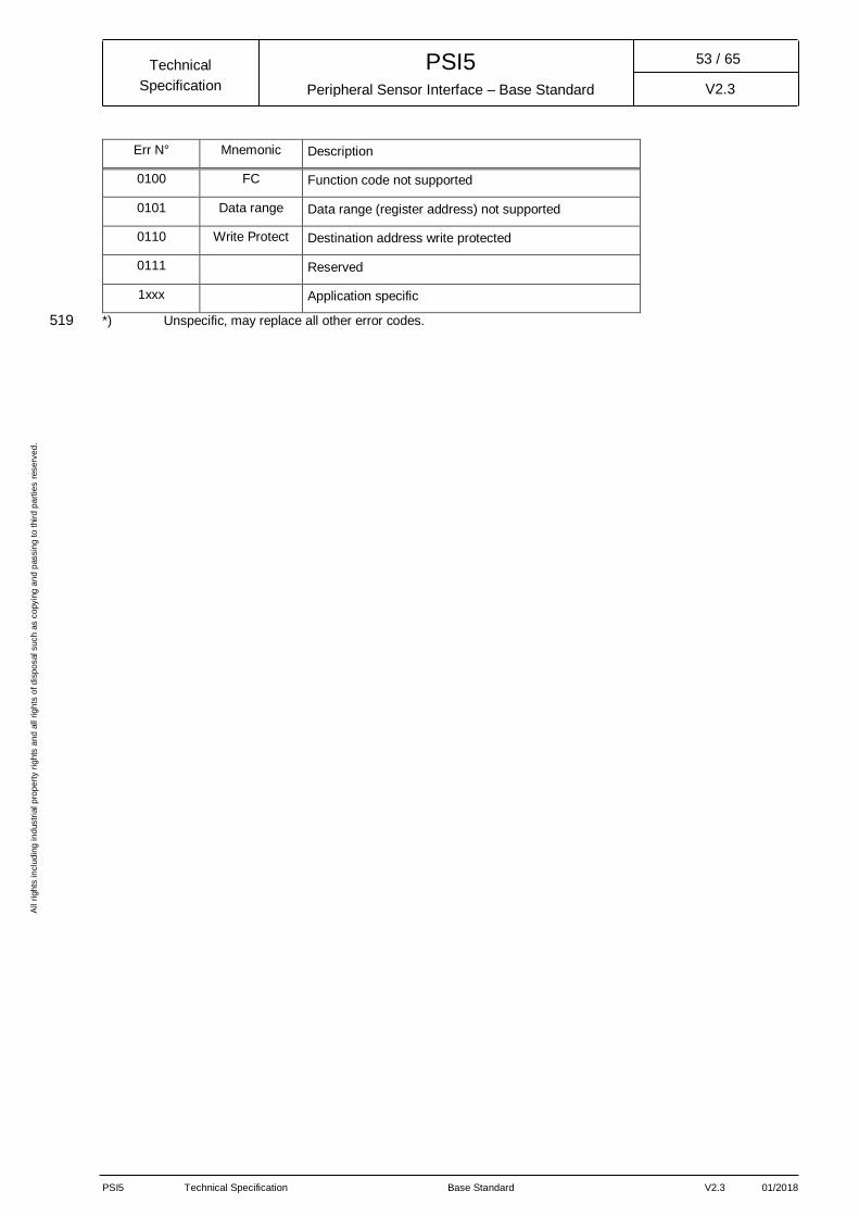
PSI5 Technical Specification Base Standard V2.3 01/2018
All r
igh
ts in
clu
din
g in
dustr
ial p
rop
ert
y r
igh
ts a
nd
all r
igh
ts o
f d
isp
osal such
as c
opyin
g a
nd
passin
g t
o t
hir
d p
art
ies
rese
rve
d.
Peripheral Sensor Interface – Base Standard
PSI5 Technical
Specification
53 / 65
V2.3
Err N° Mnemonic Description
0100 FC Function code not supported
0101 Data range Data range (register address) not supported
0110 Write Protect Destination address write protected
0111 Reserved
1xxx Application specific
*) Unspecific, may replace all other error codes. 519

PSI5 Technical Specification Base Standard V2.3 01/2018
All r
igh
ts in
clu
din
g in
dustr
ial p
rop
ert
y r
igh
ts a
nd
all r
igh
ts o
f d
isp
osal such
as c
opyin
g a
nd
passin
g t
o t
hir
d p
art
ies
rese
rve
d.
Peripheral Sensor Interface – Base Standard
PSI5 Technical
Specification
54 / 65
V2.3
6 System Setup & Operation Modes
6.1 System Setup
Figure 37 shows a possible system setup for peripheral sensors connected to an ECU with PSI5. 520
Figure 37: Connection of peripheral sensors to an ECU (Example)
The sensors are connected to the ECU by just two wires, using the same lines for power supply and data 521
transmission. The transceiver ASIC provides a pre-regulated voltage to the sensors and reads in the 522
transmitted sensor data. The example above shows a point-to-point connection for sensor 1 and 2 and two 523
different bus configurations for sensor 3 and 4, and 5 to 7, respectively. 524
6.2 PSI5 Operation Modes
The different PSI5 operation modes define topology and parameters of the communication between ECU and 525
sensors such as communication mode, number of data bits, error detection, cycle time, number of time slots 526
per cycle and bit rate. 527
InterfaceSensor 1
Sensor 2
Sensor 3 Sensor 4
Sensor 5 Sensor 7Sensor 6
µCTranceiver
ASIC
Electronic Control UnitTwo-Wire
Current InterfacePeripheral Sensors

PSI5 Technical Specification Base Standard V2.3 01/2018
All r
igh
ts in
clu
din
g in
dustr
ial p
rop
ert
y r
igh
ts a
nd
all r
igh
ts o
f d
isp
osal such
as c
opyin
g a
nd
passin
g t
o t
hir
d p
art
ies
rese
rve
d.
Peripheral Sensor Interface – Base Standard
PSI5 Technical
Specification
55 / 65
V2.3
Figure 38: Denomination of PSI5 operation modes
Example “PSI5-P10P-500/3L”: 528
PSI5 synchronous parallel bus operation, 10 data bits with parity bit, 500µs sync cycle time with three time 529
slots and a standard 125 kbps data rate. 530
Table 35: PSI5 operation modes
Communication Modes
A Asynchronous Mode
P Synchronous Parallel Bus Mode
U Synchronous Universal Bus Mode
D Synchronous Daisy Chain Bus Mode
V Variable Time Triggered Synchronous Operation Mode
Error Detection
P One Parity Bit
CRC Three Bits Cyclic Redundancy Check
Bit Rate
L 125 kbps
H 189 kbps
Cycle time
tttt cycle time in µs (e.g. 500)
or minimum allowed cycle time in µs for variable time triggered operation (e.g. 228)
/-A / P / U / D / V dd P / CRC tttt n L / H
Communication Mode
N° of Data Bits
Error Detection
Cycle time in μs
N° of Time Slots per cycle
Bit Rate

PSI5 Technical Specification Base Standard V2.3 01/2018
All r
igh
ts in
clu
din
g in
dustr
ial p
rop
ert
y r
igh
ts a
nd
all r
igh
ts o
f d
isp
osal such
as c
opyin
g a
nd
passin
g t
o t
hir
d p
art
ies
rese
rve
d.
Peripheral Sensor Interface – Base Standard
PSI5 Technical
Specification
56 / 65
V2.3
6.3 Asynchronous Operation (PSI5-A)
PSI5-A describes a point-to-point connection for unidirectional, asynchronous data transmission. Each sensor 531
is connected to the ECU by two wires. After switching on the power supply, the sensor starts transmitting data 532
to the ECU periodically. Timing and repetition rate of the data transmission are controlled by the sensor. 533
Figure 39: PSI5-A asynchronous point-to-point connection
6.4 Synchronous Operation
The synchronous operation modes work according to the TDMA method (Time Division Multiple Access). The 534
sensor data transmission is synchronized by the ECU using voltage modulation. Synchronization can optionally 535
be used for point-to-point configurations and is mandatory for bus modes. 536
S1
ECU
VSS
0V
TimingDiagram
S1 S1 S1 S1 S1
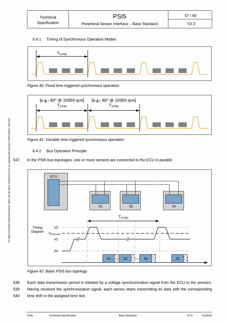
PSI5 Technical Specification Base Standard V2.3 01/2018
All r
igh
ts in
clu
din
g in
dustr
ial p
rop
ert
y r
igh
ts a
nd
all r
igh
ts o
f d
isp
osal such
as c
opyin
g a
nd
passin
g t
o t
hir
d p
art
ies
rese
rve
d.
Peripheral Sensor Interface – Base Standard
PSI5 Technical
Specification
57 / 65
V2.3
6.4.1 Timing of Synchronous Operation Modes
Figure 40: Fixed time triggered synchronous operation
Figure 41: Variable time triggered synchronous operation
6.4.2 Bus Operation Principle
In the PSI5 bus topologies, one or more sensors are connected to the ECU in parallel. 537
Figure 42: Basic PSI5 bus topology
Each data transmission period is initiated by a voltage synchronization signal from the ECU to the sensors. 538
Having received the synchronization signal, each sensor starts transmitting its data with the corresponding 539
time shift in the assigned time slot. 540
TSYNC
[e.g.: 60° @ 10000 rpm]
TSYNC
[e.g.: 60° @ 10000 rpm]
TSYNC
ECU
V2TimingDiagram
S1 S2 Sn S1
V1
0V
---
TSYNC
S1 SnS2
VThreshold

PSI5 Technical Specification Base Standard V2.3 01/2018
All r
igh
ts in
clu
din
g in
dustr
ial p
rop
ert
y r
igh
ts a
nd
all r
igh
ts o
f d
isp
osal such
as c
opyin
g a
nd
passin
g t
o t
hir
d p
art
ies
rese
rve
d.
Peripheral Sensor Interface – Base Standard
PSI5 Technical
Specification
58 / 65
V2.3
In a parallel bus configuration, an individual identification of the sensors is required. Alternatively the sensors 541
can be connected in a “Daisy Chain” configuration to the ECU. In this configuration the sensors have no fixed 542
address and can be connected to each position on the bus. During startup, each sensor receives an individual 543
address and then passes the supply voltage to the following sensor subsequently. The addressing is realized 544
by bidirectional communication from the ECU to the sensor using a specific sync signal pattern. After having 545
assigned the individual addresses, the sensors start to transmit data in their corresponding time slots in the 546
same way as specified in the parallel bus topology. 547
Figure 43: Daisy chain bus topology
6.4.2.1 Preferred Daisy-Chain Mode: Parallel Initialization Phase4)
The aim of this section is to provide some guidelines applicable for a PSI5 interface when it is operated in 548
Daisy-Chain mode, and especially to enhance the application layer specification for this mode. 549
In this operation mode, each sensor sends out the initialization sequence over the previously assigned sensor 550
time slot. The timeslot is assigned by an address setting instruction. The ECU shall assign the addresses in 551
reverse order, i.e. that timeslot TS1 is the last one receiving its address. Furthermore, timeslot TS1 is defined 552
as being the default timeslot for sensor error reporting in case of an unsuccessful address assignment. 553
Principle of operation 554
1. ECU applies supply voltage to PSI5 Interface (power on) 555
4) Valid from PSI5 Technical Specification V2.1 onwards and for all Substandards except Powertrain Substandard. For
backward compatibility with PSI5 V1.3 for airbag application a thorough description is given within the Airbag Substandard.
S1
Sn
SnS2
ECU
V2
TimingDiagram
S1
V1
0V
TSYNC
VThreshold
S1 S2 ---
Tslot
AddresingSequence
Run Mode
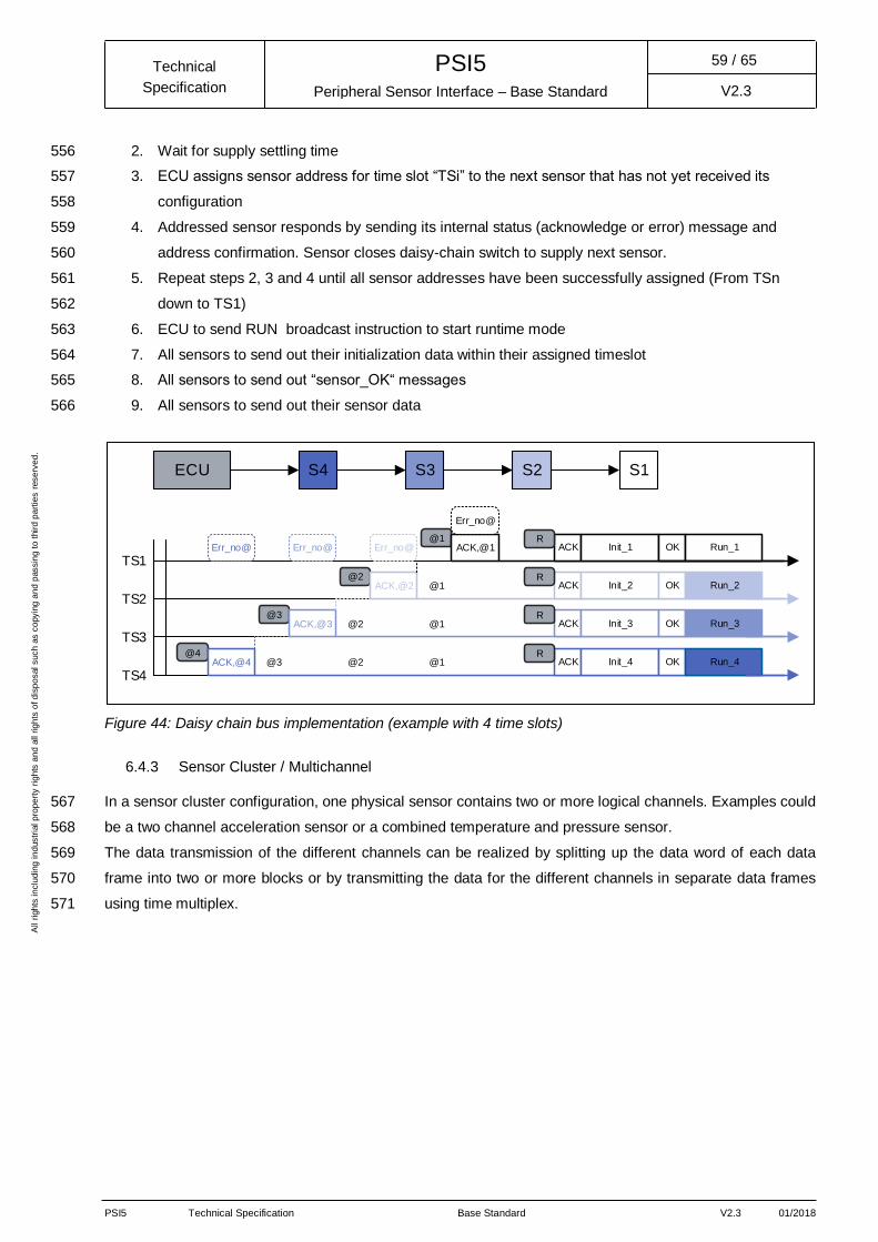
PSI5 Technical Specification Base Standard V2.3 01/2018
All r
igh
ts in
clu
din
g in
dustr
ial p
rop
ert
y r
igh
ts a
nd
all r
igh
ts o
f d
isp
osal such
as c
opyin
g a
nd
passin
g t
o t
hir
d p
art
ies
rese
rve
d.
Peripheral Sensor Interface – Base Standard
PSI5 Technical
Specification
59 / 65
V2.3
2. Wait for supply settling time 556
3. ECU assigns sensor address for time slot “TSi” to the next sensor that has not yet received its 557
configuration 558
4. Addressed sensor responds by sending its internal status (acknowledge or error) message and 559
address confirmation. Sensor closes daisy-chain switch to supply next sensor. 560
5. Repeat steps 2, 3 and 4 until all sensor addresses have been successfully assigned (From TSn 561
down to TS1) 562
6. ECU to send RUN broadcast instruction to start runtime mode 563
7. All sensors to send out their initialization data within their assigned timeslot 564
8. All sensors to send out “sensor_OK“ messages 565
9. All sensors to send out their sensor data 566
Figure 44: Daisy chain bus implementation (example with 4 time slots)
6.4.3 Sensor Cluster / Multichannel
In a sensor cluster configuration, one physical sensor contains two or more logical channels. Examples could 567
be a two channel acceleration sensor or a combined temperature and pressure sensor. 568
The data transmission of the different channels can be realized by splitting up the data word of each data 569
frame into two or more blocks or by transmitting the data for the different channels in separate data frames 570
using time multiplex. 571
@1
@1
@1
@2
@2@3
ECU S4 S3 S2 S1
@4ACK
@1ACK,@1
@2
@3ACK
ACK
ACKR
R
R
R
Init_1 OK Run_1
Init_2 OK Run_2
Init_3 OK Run_3
Init_4 OK Run_4
ACK,@3
ACK,@4
ACK,@2
TS1
TS2
TS3
TS4
Err_no@ Err_no@
Err_no@
Err_no@

PSI5 Technical Specification Base Standard V2.3 01/2018
All r
igh
ts in
clu
din
g in
dustr
ial p
rop
ert
y r
igh
ts a
nd
all r
igh
ts o
f d
isp
osal such
as c
opyin
g a
nd
passin
g t
o t
hir
d p
art
ies
rese
rve
d.
Peripheral Sensor Interface – Base Standard
PSI5 Technical
Specification
60 / 65
V2.3
Figure 45: Implementation example sensor cluster
Sensor cluster / multichannel operation modes can be combined with both asynchronous and synchronous 572
data transmission and with the different bus configurations. 573
S1
ECU
Ch BCh A
Ch BCh AS1 Ch BCh AS1 Ch BCh AS1
Ch AS1 Ch BS1 Ch AS1 Ch BS1 Ch AS1 ...
... t
t
Multiple channeltransmission usingone data word
Time multiplexeddata transmission

PSI5 Technical Specification Base Standard V2.3 01/2018
All r
igh
ts in
clu
din
g in
dustr
ial p
rop
ert
y r
igh
ts a
nd
all r
igh
ts o
f d
isp
osal such
as c
opyin
g a
nd
passin
g t
o t
hir
d p
art
ies
rese
rve
d.
Peripheral Sensor Interface – Base Standard
PSI5 Technical
Specification
61 / 65
V2.3
7 Interoperability Requirements
PSI5 defines all basic characteristics of an electrical sensor interface including the physical layer, data link 574
layer and - to a certain extend - the application layer. Interoperability between ECU and sensors (asynchronous 575
/ synchronous mode) or bus (parallel / universal bus mode and daisy chain mode) requires the definition of the 576
following additional, system specific parameters: 577
Sensor configurations, operation modes and timings (single sensor, bus configuration or sensor cluster) 578
System supply voltage (low, standard or increased) 579
Current driving capabilities vs. current load of the sensors (standard or extended) 580
Initialization data content i.e. also including determination of the repetition count (k) 581
Other sensor parameters such as mechanical and dimensional characteristics, signal evaluation path and 582
functional characteristics or reliability and environmental test conditions are beyond the scope of the PSI5 583
specification and have to be specified in separate documents to assure cross compatibility. 584

PSI5 Technical Specification Base Standard V2.3 01/2018
All r
igh
ts in
clu
din
g in
dustr
ial p
rop
ert
y r
igh
ts a
nd
all r
igh
ts o
f d
isp
osal such
as c
opyin
g a
nd
passin
g t
o t
hir
d p
art
ies
rese
rve
d.
Peripheral Sensor Interface – Base Standard
PSI5 Technical
Specification
62 / 65
V2.3
8 Document History & Modifications
Rev.N° Chapter Description / Changes Date
1.0 all First Edition 15.07.2005
1.1 div. see Version 1.1 30.06.2006
1.2 1.2 Optional 189kbps data transmission speed added 12.06.2007
2.3 Synchronous operation: new denomination for operation modes
2.3.2 Serial topology: changed form voltage shift method to low-side
“daisy chain” switching with bidirectional addressing sequence
3.3.1 Data Range: Updated Status & Error Messages
3.3.2 Scaling of data range: definition for initialization data added
3.4.1 Description of Initialization phase extended
3.4.2 Initialization data content summarized in Chapter 3.4.3;
Mandatory header information includes F5 - sensor parameter.
4 Structure of parameter specification reorganized;
General parameters (4.1) :
- Quiescent current 4 .. 19mA, extended current max. 35mA
- Current limitation added
Data transmission parameters (4.4) :
- correction of start bit values in the data frame timing figure
- bit time for 189kbps mode added
- communication current tolerance narrowed
- fall / rise time communication current changed (see Chapter 5)
- clock drift rate specified
Synchronization signal (4.5):
- detailed specification of only one, unified sync signal
Timing of synchronous operation modes (4.6):
- specification of time slots
5 System configurations (new Chapter):
- denomination of PSI5 operating modes specified (5.1)
- recommended operating modes (5.2)
- detailed system configuration: asynchronous operation (5.4)
- detailed system configuration: parallel bus modes (5.5.1,
5.5.2)
- detailed system configuration: serial bus mode (5.6)
- reference networks & test conditions (5.7)
- operation modes PSI5-P10P (5.8)
1.3 div. Siemens VDO replaced by Continental 06.06.2008
2.2 Shifted from Chapter 5.

PSI5 Technical Specification Base Standard V2.3 01/2018
All r
igh
ts in
clu
din
g in
dustr
ial p
rop
ert
y r
igh
ts a
nd
all r
igh
ts o
f d
isp
osal such
as c
opyin
g a
nd
passin
g t
o t
hir
d p
art
ies
rese
rve
d.
Peripheral Sensor Interface – Base Standard
PSI5 Technical
Specification
63 / 65
V2.3
Denomination of operation modes changed:
- Asynchron
- Parallel Bus (Parallel Configuration)
- Universal Bus (Pass-Through Configuration)
- Daisy Chain Bus (Serial Configuration)
2.3;2.4 Simplified diagrams of sensor configurations shifted from
Chapter 5
3 Chapter renamed: Sensor to ECU Communication
3.4.4 Diagnostic Mode added.
4 Chapter added: ECU to Sensor Communication
5.1.1 Reverse polarity protection:
- 100ms replaced by 80ms and 50ms respectively
- min value of 105mA for standard mode
5.1.2 - Supply voltage for Universal Bus and Daisy Chain Bus added
- Daisy Chain Sensor Quiescent Current added
5.2 Optional settling time for Daisy Chain Bus added
5.3 Figure replaced for clarity
6.3 Min value for capacitive sensor bus load changed to 6nF
6.4 Parameter Specification for Universal Bus added
6.5 Parameter Specification for Daisy Chain Bus added
6.6.1 - Definition of max value for supply voltage instead of nominal
value
- Definition of min and max value for ECU internal capacitance
instead of nominal value
- Sensor damping behavior redefined
6.6.2 Reference network for Universal Bus Mode and Daisy Chain Bus
Mode added
7.2 Recommended Configurations shifted from Chapter 5.2
2.0 Full revision; plus technical changes, amendments and formal
changes of the document structure. Application specific
Substandards “airbag”, “vehicle dynamics control” and
“powertrain” are added to the PSI5 “Base Standard” document.
Main features are:
Changes to Physical Layer: optional Vss voltage level 4,0V;
bidirectional communication downstream with short & long sync
signal; optional reduced sync voltage; reduced sending current
Changes to Data Link Layer: enhanced data word length up to
28bit; initialization option based on "Serial Channel"
06/2011
2.1 Full revision plus technical changes (see below) 10/2012

PSI5 Technical Specification Base Standard V2.3 01/2018
All r
igh
ts in
clu
din
g in
dustr
ial p
rop
ert
y r
igh
ts a
nd
all r
igh
ts o
f d
isp
osal such
as c
opyin
g a
nd
passin
g t
o t
hir
d p
art
ies
rese
rve
d.
Peripheral Sensor Interface – Base Standard
PSI5 Technical
Specification
64 / 65
V2.3
2.4.2 Daisy Chain implementation added
3.2 Explicit definition added that both start bits always are coded as
two "zeros"
3.3.1
- Signification for reserved Data in Data Range 1 and 2 changed
- Status & Error Messages; signification +489 "Sensor in
Diagnostic Mode" renamed
4.1 Tooth Gap Method connected to the usage of the "short" sync
pulse only
5.2.2 Xlong Data Frame: Definition of Sensor Response RD2 added
6.2 settling time quiescent current changed to 10ms
6.3 Undervoltage Reset and Microcut Rejection; split definition in
base document (general) and Substandard (application specific
min/max values for the affected parameters)
6.4 Sensor clock deviation during data frame widened for Chassis
and power train applications, two alternative options defined in
base specification (0.1%; 1%)
6.6.1 Additional explanations given for time slot calculation
7.6.4
7.7
Change of Test Parameter Specification, ECU reference test
added, additional explanations.
div. Editorial changes, consecutive line numbers for traceability
2.2 1.1 Updated members 05/2016
3.4 Example of CRC Calculation
5.1.2 Added section “Data Content – Data Range Initialization”
6.1 New parameter definition “signal noise limit” and “quiescent
current drift rate”; detailed explanation of absolute maximum
ratings
6.1.2 Quiescent current drift rate changed from 1 mA/s to 10 mA/s
6.1.2 Sync signal upper boundary (16.5V)
6.1.2 Signal noise limit defined (+/- 2mA for common mode)
6.2.1 New Chapter “Sensor Bus Configuration”, settling time quiescent
current changed to 5ms (larger settling times to be addressed in
new Chapter “extended settling time”)
6.2.2 New Chapter “6.2.2 Extended Settling Time for single sensor
configuration”
6.4 Maximum sensor clock deviation during data frame changed
from 0.1% to 1%.
div. Editorial changes, Term “recommended” mainly removed from
standard. Standardization of document naming.

PSI5 Technical Specification Base Standard V2.3 01/2018
All r
igh
ts in
clu
din
g in
dustr
ial p
rop
ert
y r
igh
ts a
nd
all r
igh
ts o
f d
isp
osal such
as c
opyin
g a
nd
passin
g t
o t
hir
d p
art
ies
rese
rve
d.
Peripheral Sensor Interface – Base Standard
PSI5 Technical
Specification
65 / 65
V2.3
2.3 2 Chapter “Definition of Terms” introduced with Symbol/Parameter
Definitions, Glossary and Acronyms, Abbreviations
31.07.2017
3 Chapter “Data Link Layer” introduced which consolidates all
relevant definitions concerning PSI5 data link layer; consolidated
information deleted out of former chapters
4 Chapter “Physical Layer” introduced which consolidates all
relevant definitions concerning PSI5 physical layer; consolidated
information deleted out of former chapters
4.7.1 Chapter “Supply and Communication Parameters Definitions”
introduced.
Figure 22: System current and voltage definitions added.
Table 15: Parameter specification of absolute maximum ratings
added which defines common and low power mode with related
physical layer compilations
4.7.3 Definitions and explanations for Supply Voltages, Supply Voltage
operation options and Interface Current operation options added.
Former separate table for Common Mode and Low Power Mode
consolidated in Table 16: Parameter compilation for Common
Mode and Low Power Mode operation
4.9 Explanation added for different sync pulse levels with linked
parameters
4 Introduced “Conditions/Remark” column to all tables
div. Table captions and list of tables added.
List of figures added.
All figures have been redrawn.
Line numbering has been completely reworked.
Document has been completely reformatted.
.