Embed Size (px)
Citation preview

PERI INSTITUTE OF TECHNOLOGY
Department Of Electrical and Electronics Engineering
Mannivakkam, Chennai – 600 048
Model Answer Key
Year/Sem: III/VI Max Marks: 100
Sub Code/ Name: EE2354/Microprocessor and Micro Controller Duration: 3Hrs
PART A 10*2=20
1. What are the important control signals in 8085 microprocessor?
The important control signals in 8085 microprocessor are SIM and RIM.
2. State the uses of ALE signal in 8085.
ALE is address latch enable, it is used for demultiplex the address lines.
3. What is different between DCR and DCX instruction?
DCR: Decrement the register contentment by 1. DCX: Decrement the register pair contentment by 1.
4. Name the machine control instruction in 8085.
SIM, RIM, DI, EI, HLT and NOP.
5. Write the format of control word for 8255 PPI.
6. What is the cascade mode of 8259 programmable interrupt controller?
To expand the interrupt handling capacity to sixty four level.
7. Give the memory size of 8051.
The memory size of 8051 is 4KB * 8 ROM, 128 * 8 RAM, 64KB address space for external data memory &
Program memory.
8. Name the interrupt available in 8051.
INT0, INT1, TIMER0, TIMER1 and Serial Port
9. List out the varies operations performed by Boolean variable instruction of 8051.
The Boolean variable instruction of 8051 are AND, OR, and XOR.
10. What are the operating modes of serial port of 8051?
The operation modes of serial port 8051 are Synchronous and Asynchronous mode.
www.vidyarthiplus.com1 of 24.
Footer Page 1 of 24.

PART B 5*16=80
11. a. Draw and explain interfacing of memory with 8085 and its interrupt structure.
www.vidyarthiplus.com2 of 24.
Footer Page 2 of 24.

www.vidyarthiplus.com3 of 24.
Footer Page 3 of 24.
www.vidyarthiplus.com4 of 24.
Footer Page 4 of 24.
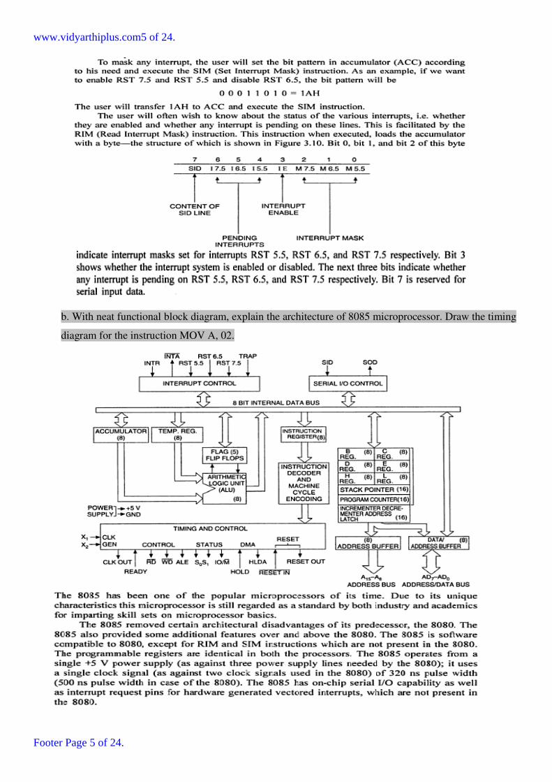
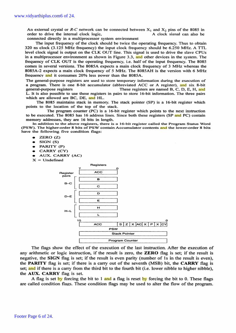
b. With neat functional block diagram, explain the architecture of 8085 microprocessor. Draw the timing
diagram for the instruction MOV A, 02.
www.vidyarthiplus.com5 of 24.
Footer Page 5 of 24.
www.vidyarthiplus.com6 of 24.
Footer Page 6 of 24.
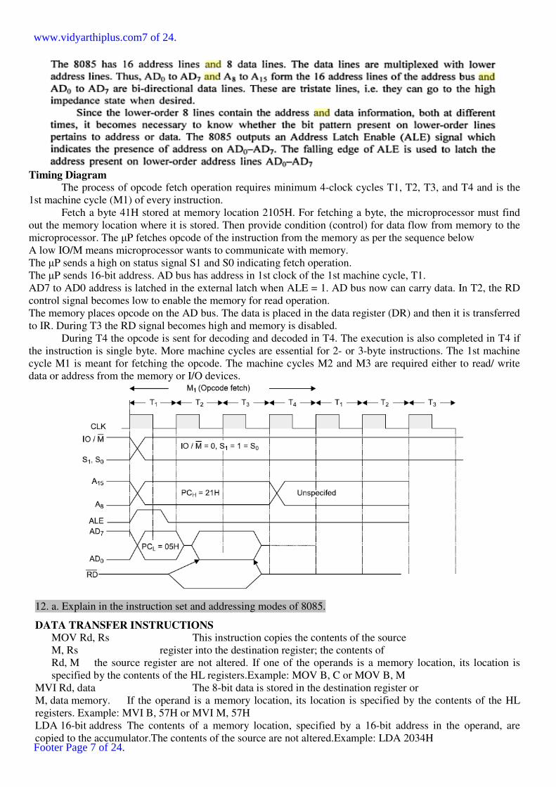
Timing Diagram
The process of opcode fetch operation requires minimum 4-clock cycles T1, T2, T3, and T4 and is the
1st machine cycle (M1) of every instruction.
Fetch a byte 41H stored at memory location 2105H. For fetching a byte, the microprocessor must find
out the memory location where it is stored. Then provide condition (control) for data flow from memory to the
microprocessor. The µP fetches opcode of the instruction from the memory as per the sequence below
A low IO/M means microprocessor wants to communicate with memory.
The µP sends a high on status signal S1 and S0 indicating fetch operation.
The µP sends 16-bit address. AD bus has address in 1st clock of the 1st machine cycle, T1.
AD7 to AD0 address is latched in the external latch when ALE = 1. AD bus now can carry data. In T2, the RD
control signal becomes low to enable the memory for read operation.
The memory places opcode on the AD bus. The data is placed in the data register (DR) and then it is transferred
to IR. During T3 the RD signal becomes high and memory is disabled.
During T4 the opcode is sent for decoding and decoded in T4. The execution is also completed in T4 if
the instruction is single byte. More machine cycles are essential for 2- or 3-byte instructions. The 1st machine
cycle M1 is meant for fetching the opcode. The machine cycles M2 and M3 are required either to read/ write
data or address from the memory or I/O devices.
12. a. Explain in the instruction set and addressing modes of 8085.
DATA TRANSFER INSTRUCTIONS
MOV Rd, Rs This instruction copies the contents of the source
M, Rs register into the destination register; the contents of
Rd, M the source register are not altered. If one of the operands is a memory location, its location is
specified by the contents of the HL registers.Example: MOV B, C or MOV B, M
MVI Rd, data The 8-bit data is stored in the destination register or
M, data memory. If the operand is a memory location, its location is specified by the contents of the HL
registers. Example: MVI B, 57H or MVI M, 57H
LDA 16-bit address The contents of a memory location, specified by a 16-bit address in the operand, are
copied to the accumulator.The contents of the source are not altered.Example: LDA 2034H
www.vidyarthiplus.com7 of 24.
Footer Page 7 of 24.

LDAX B/D Reg. pair The contents of the designated register pair point to a memory location. This
instruction copies the contents of that memory location into the accumulator. The contents of either the
register pair or the memory location are not altered.Example: LDAX B
LXI Reg. pair, 16-bit data The instruction loads 16-bit data in the register pair designated in the operand.
Example: LXI H, 2034H or LXI H, XYZ
LHLD 16-bit address The instruction copies the contents of the memory location pointed out by the 16-
bit address into register L and copies the contents of the next memory location into register H. The contents of
source memory locations are not altered. Example: LHLD 2040H
STA 16-bit address The contents of the accumulator are copied into the memory location specified by he
operand. This is a 3-byte instruction, the second byte specifies the low-order address and the third byte
specifies the high-order address. Example: STA 4350H
STAX Reg. pair The contents of the accumulator are copied into the memory location specified by the
contents of the operand (register pair). The contents of the accumulator are not altered. Example: STAX B
SHLD 16-bit address The contents of register L are stored into the memory location specified by the 16-
bit address in the operand and the contents of H register are stored into the next memory location by
incrementing the operand. The contents of registers HL are not altered. This is a 3-byte instruction, the second
byte specifies the low-order address and the third byte specifies thehigh-order address.Example: SHLD 2470H
XCHG none The contents of register H are exchanged with the contents of register D, and the contents of
register L are exchanged with the contents of register E. Example: XCHG
SPHL none The instruction loads the contents of the H and L registers into the stack pointer register, the
contents of the H register provide the high-order address and the contents of the L register provide the low-
order address. The contents of the H and L registers are not altered. Example: SPHL
XTHL none The contents of the L register are exchanged with the stack location pointed out by the contents
of the stack pointer register. The contents of the H register are exchanged with the next stack location (SP+1);
however, the contents of the stack pointer register are not altered. Example: XTHL
PUSH Reg. pair The contents of the register pair designated in the operand are copied onto the stack in the
following sequence. The stack pointer register is decremented and the contents of the highorder register (B, D,
H, A) are copied into that location. The stack pointer register is decremented again and the contents of the
low-order register (C, E, L, flags) are copied to that location. Example: PUSH B or PUSH A
POP Reg. pair The contents of the memory location pointed out by the stack pointer register are copied
to the low-order register (C, E, L, status flags) of the operand. The stack pointer is incremented by 1 and the
contents of that memory location are copied to the high-order register (B, D, H, A) of the operand. The stack
pointer register is again incremented by 1. Example: POP H or POP A
OUT 8-bit port address The contents of the accumulator are copied into the I/O port specified by the
operand. Example: OUT F8H
IN 8-bit port address The contents of the input port designated in the operand are read and loaded into
the accumulator. Example: IN 8CH
ARITHMETIC INSTRUCTIONS
ADD R The contents of the operand (register or memory) are M added to the contents of the accumulator
and the result is stored in the accumulator. If the operand is a memory location, its location is specified by the
contents of the HL registers. All flags are modified to reflect the result of the addition. Example: ADD B or
ADD M
ADC R The contents of the operand (register or memory) and M the Carry flag are added to the contents
of the accumulator and the result is stored in the accumulator. If the operand is a memory location, its location
is specified by the contents of the HL registers. All flags are modified to reflect the result of the addition.
Example: ADC B or ADC M
ADI 8-bit data The 8-bit data (operand) is added to the contents of the accumulator and the result is
stored in the accumulator. All flags are modified to reflect the result of the addition. Example: ADI 45H
ACI 8-bit data The 8-bit data (operand) and the Carry flag are added to the contents of the accumulator
and the result is stored in the accumulator. All flags are modified to reflect the result of the addition. Example:
ACI 45H
DAD Reg. pair The 16-bit contents of the specified register pair are added to the contents of the HL
register and the sum is stored in the HL register. The contents of the source register pair are not altered. If the
result is larger than 16 bits, the CY flag is set.No other flags are affected. Example: DAD H
www.vidyarthiplus.com8 of 24.
Footer Page 8 of 24.
SUB R The contents of the operand (register or memory ) are M subtracted from the contents of the
accumulator, and the result is stored in the accumulator. If the operand is a memory location, its location is
specified by the contents of the HL registers. All flags are modified to reflect the result of the subtraction.
Example: SUB B or SUB M
SBB R The contents of the operand (register or memory ) and M the Borrow flag are subtracted from the
contents of the accumulator and the result is placed in the accumulator. If the operand is a memory location, its
location is specified by the contents of the HL registers. All flags are modified to reflect the result of the
subtraction. Example: SBB B or SBB M
SUI 8-bit data The 8-bit data (operand) is subtracted from the contents of the accumulator and the result
is stored in the accumulator. All flags are modified to reflect the result of the subtraction. Example: SUI 45H
SBI 8-bit data The 8-bit data (operand) and the Borrow flag are subtracted from the contents of the
accumulator and the result is stored in the accumulator. All flags are modified to reflect the result of the
subtracion. Example: SBI 45H
INR R The contents of the designated register or memory) are M incremented by 1 and the result is
stored in the same place. If the operand is a memory location, its location is specified by the contents of the
HL registers. Example: INR B or INR M
INX R The contents of the designated register pair are incremented by 1 and the result is stored in the
same place. Example: INX H
DCR R The contents of the designated register or memory are M decremented by 1 and the result is
stored in the same place. If the operand is a memory location, its location is specified by the contents of the
HL registers. Example: DCR B or DCR M
DCX R The contents of the designated register pair are decremented by 1 and the result is stored in the
same place. Example: DCX H
DAA none The contents of the accumulator are changed from a binary value to two 4-bit binary coded
decimal (BCD) digits. This is the only instruction that uses the auxiliary flag to perform the binary to BCD
conversion, and the conversion procedure is described below. S, Z, AC, P, CY flags are altered to reflect the
results of the operation. If the value of the low-order 4-bits in the accumulator is greater than 9 or if AC flag is
set, the instruction adds 6 to the low-order four bits. If the value of the high-order 4-bits in the accumulator is
greater than 9 or if the Carry flag is set, the instruction adds 6 to the high-order four bits. Example: DAA
BRANCHING INSTRUCTIONS
JMP 16-bit address The program sequence is transferred to the memory location specified by the 16-bit
address given in the operand. Example: JMP 2034H or JMP XYZ
Jump conditionally 16-bit addThe program sequence is transferred to the memory location specified by the 1-
bit address given in the operand based on the specified flag of the PSW as described below. Example: JZ
2034H or JZ XYZ
JC Jump on Carry CY = 1 JNC Jump on no Carry CY = 0 JP Jump on positive S = 0 JM Jump on minus S = 1
JZ Jump on zero Z = 1 JNZ Jump on no zero Z = 0 JPE Jump on parity even P = 1 JPO Jump on parity odd P
= 0
CALL 16-bit address The program sequence is transferred to the memory location specified by the 16-
bit address given in the operand. Before the transfer, the address of the next instruction after CALL (the
contents of the program counter) is pushed onto the stack. Example: CALL 2034H or CALL XYZ
Call conditionally 16-bit add The program sequence is transferred to the memory location specified by
the 16-bit address given in the operand based on the specified flag of the PSW as described below. Before the
transfer, the address of the next instruction after the call (the contents of the program counter) is pushed onto
the stack. Example: CZ 2034H or CZ XYZ
CC Call on Carry CY = 1 CNC Call on no Carry CY = 0 CP Call on positive S = 0 CM Call on minus S = 1
CZ Call on zero Z = 1 CNZ Call on no zero Z = 0 CPE Call on parity even P = 1 CPO Call on parity odd P = 0
RET none The program sequence is transferred from the subroutine to the calling program. The two bytes
from the top of the stack are copied into the program counter, and program execution begins at the new
address. Example: RET
Return from subroutine conditionally The program sequence is transferred from the subroutine to the calling
program based on the specified flag of the PSW as described below. The two bytes from the top of the stack
are copied into the program counter, and program execution begins at the new address. Example: RZ
www.vidyarthiplus.com9 of 24.
Footer Page 9 of 24.

RC Return on Carry CY = 1 RNC Return on no Carry CY = 0 RP Return on positive S = 0 RM Return on
minus S = 1 RZ Return on zero Z = 1 RNZ Return on no zero Z = 0 RPE Return on parity even P = 1 RPO
Return on parity odd P = 0
PCHL none The contents of registers H and L are copied into the program counter. The contents of H are
placed as the high-order byte and the contents of L as the low-order byte. Example: PCHL
Restart The RST instruction is equivalent to a 1-byte call instruction to one of eight memory locations
depending upon the number. The instructions are generally used in conjunction with interrupts and inserted
using external hardware. However these can be used as software instructions in a program to transfer program
execution to one of the eight locations. The addresses are:
Instruction Restart Address
RST 0 0000H RST 1 0008H RST 2 0010H RST 3 0018H RST 4 0020H RST 5 0028H RST 6 0030H RST 7
0038H
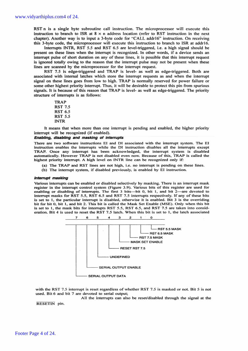
The 8085 has four additional interrupts and these interrupts generate RST instructions internally and thus do
not require any external hardware. These instructions and their Restart addresses are:
Interrupt Restart Address TRAP 0024H RST 5.5 002CH RST 6.5 0034H RST 7.5 003CH
LOGICAL INSTRUCTIONS
CMP R The contents of the operand (register or memory) are M compared with the contents of the
accumulator. Both contents are preserved . The result of the comparison is shown by setting the flags of the
PSW as follows: if (A) < (reg/mem): carry flag is set if (A) = (reg/mem): zero flag is set if (A) > (reg/mem):
carry and zero flags are reset Example: CMP B or CMP M
CPI 8-bit data The second byte (8-bit data) is compared with the contents of the accumulator. The
values being compared remain unchanged. The result of the comparison is shown by setting the flags of the
PSW as follows: if (A) < data: carry flag is set if (A) = data: zero flag is set if (A) > data: carry and zero flags
are reset Example: CPI 89H
ANA R The contents of the accumulator are logically ANDed with M the contents of the operand
(register or memory), and the result is placed in the accumulator. If the operand is a memory location, its
address is specified by the contents of HL registers. S, Z, P are modified to reflect the result of the operation.
CY is reset. AC is set. Example: ANA B or ANA M
ANI 8-bit data The contents of the accumulator are logically ANDed with the 8-bit data
(operand) and the result is placed in the accumulator. S, Z, P are modified to reflect the result of the operation.
CY is reset. AC is set. Example: ANI 86H
XRA R The contents of the accumulator are Exclusive ORed with M the contents of the operand (register
or memory), and the result is placed in the accumulator. If the operand is a memory location, its address is
specified by the contents of HL registers. S, Z, P are modified to reflect the result of the operation. CY and AC
are reset. Example: XRA B or XRA M
XRI 8-bit data The contents of the accumulator are Exclusive ORed with the 8-bit data (operand) and the
result is placed in the accumulator. S, Z, P are modified to reflect the result of the operation. CY and AC are
reset. Example: XRI 86H
ORA R The contents of the accumulator are logically ORed with M the contents of the operand (register
or memory), and the result is placed in the accumulator. If the operand is a memory location, its address is
specified by the contents of HL registers. S, Z, P are modified to reflect the result of the operation. CY and AC
are reset. Example: ORA B or ORA M
ORI 8-bit data The contents of the accumulator are logically ORed with the 8-bit data (operand) and the
result is placed in the accumulator. S, Z, P are modified to reflect the result of the operation. CY and AC are
reset. Example: ORI 86H
RLC none Each binary bit of the accumulator is rotated left by one position. Bit D7 is placed in the position
of D0 as well as in the Carry flag. CY is modified according to bit D7. S, Z, P, AC are not affected.
Example: RLC
RRC none Each binary bit of the accumulator is rotated right by one position. Bit D0 is placed in the
position of D7 as well as in the Carry flag. CY is modified according to bit D0. S, Z, P, AC are not affected.
Example: RRC
RAL none Each binary bit of the accumulator is rotated left by one position through the Carry flag. Bit D7
is placed in the Carry flag, and the Carry flag is placed in the least significant position D0. CY is modified
according to bit D7. S, Z, P, AC are not affected. Example: RAL
www.vidyarthiplus.com10 of 24.
Footer Page 10 of 24.
RAR none Each binary bit of the accumulator is rotated right by one position through the Carry flag. Bit D0
is placed in the Carry flag, and the Carry flag is placed in the most significant position D7. CY is modified
according to bit D0. S, Z, P, AC are not affected. Example: RAR
CMA none The contents of the accumulator are complemented. No flags are affected.
Example: CMA
CMC none The Carry flag is complemented. No other flags are affected. Example: CMC
STC none The Carry flag is set to 1. No other flags are affected. Example: STC
CONTROL INSTRUCTIONS
NOP none No operation is performed. The instruction is fetched and decoded. However no operation is
executed. Example: NOP
HLT none The CPU finishes executing the current instruction and halts any further execution. An interrupt
or reset is necessary to exit from the halt state. Example: HLT
DI none The interrupt enable flip-flop is reset and all the interrupts except the TRAP are disabled. No
flags are affected. Example: DI
EI none The interrupt enable flip-flop is set and all interrupts are enabled. No flags are affected. After a
system reset or the acknowledgement of an interrupt, the interrupt enable flipflop is reset, thus disabling the
interrupts. This instruction is necessary to reenable the interrupts (except TRAP). Example: EI
RIM none This is a multipurpose instruction used to read the status of interrupts 7.5, 6.5, 5.5 and read serial
data input bit. The instruction loads eight bits in the accumulator with the following interpretations. Example:
RIM
SIM none This is a multipurpose instruction and used to implement the 8085 interrupts 7.5, 6.5, 5.5, and
serial data output. The instruction interprets the accumulator contents as follows. Example: SIM
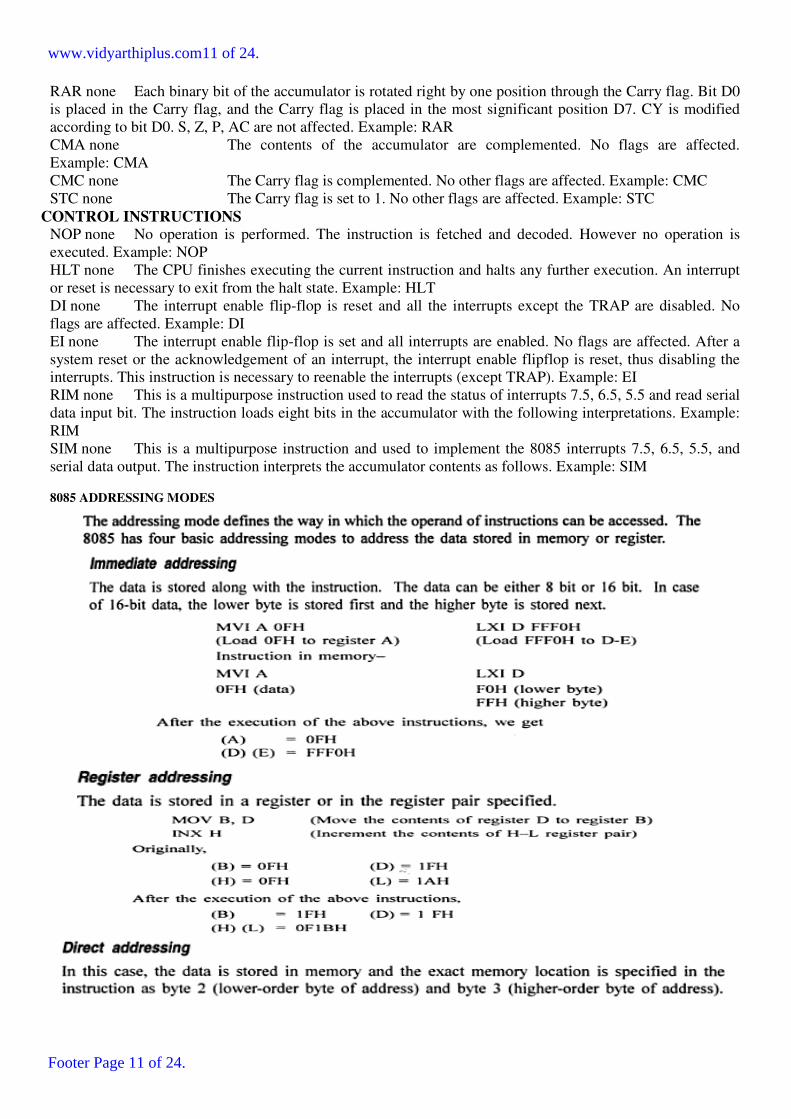
8085 ADDRESSING MODES
www.vidyarthiplus.com11 of 24.
Footer Page 11 of 24.
Implicit Addressing Mode
If address of source of data as well as address of destination of result is fixed, then there is no need to give
any operand along with the instruction.
CMA is the operation. A is the source. A is the destination.
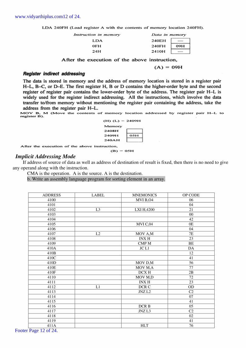
b. Write an assembly language program for sorting element in an array.
ADDRESS LABEL MNEMONICS OP CODE
4100 MVI B,O4 06
4101 04
4102 L3 LXI H,4200 21
4103 00
4104 42
4105 MVI C,04 0E
4106 04
4107 L2 MOV A,M 7E
4108 INX H 23
4109 CMP M BE
410A JC L1 DA
410B 12
410C 41
410D MOV D,M 56
410E MOV M,A 77
410F DCX H 2B
4110 MOV M,D 72
4111 INX H 23
4112 L1 DCR C OD
4113 JNZ L2 C2
4114 07
4115 41
4116 DCR B 05
4117 JNZ L3 C2
4118 02
4119 41
411A HLT 76
www.vidyarthiplus.com12 of 24.
Footer Page 12 of 24.

13. a. With suitable diagram explain the working principle of 8253 timer.
The 8253/54 solves one of most common problem in any microcomputer system, the generation of accurate
time delays under software control. Instead of setting up timing loops in system software, the programmer
configures the 8253/54 to match his requirements, initializes one of the counters of the 8253/54 with the
desired quantity, then upon command the 8253/54 will count out the delay and interrupt the CPU when it has
completed its tasks. It is easy to see that the software overhead is minimum and that multiple delays can be
easily be maintained by assignment of priority levels. The 8253/54 includes three identical 16 bit counters that
can operate independently. To operate a counter, a 16-bit count is loaded in its register and, on command, it
begins to decrement the count until it reaches 0. At the end of the count, it generates a pulse that can be used to
interrupt the CPU. The counter can count either in binary or BCD.
In addition, a count can be read by the CPU while the counter is decrementing. In this chapter, we are going to
study two timer ICs 8253 and 8254. The 8254 is a superset of 8253. The functioning of these two ICs are
almost similar along with the pin configuration. Only the differences are :
8253 8254
1. Operating frequency 0 - 2.6 MHz. 1. Operating frequency 0 - 10 MHz.
2. Uses N-MOS technology 2. Uses H-MOS technology.
3. Read-Back command not available. 3. Read-Back command available.
4. Reads and writes of the same counter can
not be interleaved.
4. Reads and writes of the same counter can be
interleaved.
Data Bus Buffer :
This tri-state, bi-directional, 8-bit buffer is used to interface the 8253/54 to the system data bus. The Data
bus buffer has three basic functions.
1. Programming the modes of 8253/54.2. Loading the count registers.3. Reading the count values.
Read/Write Logic : The Read/Write logic has five signals : RD, WR, CS and the address lines A0 and
A1. In the peripheral I/O mode, the RD, and WR signals are connected to IOR and IOW, respectively. In
memory-mapped I/O, these are connected to MEMR and MEMW. Address lines A0 and A1 of the CPU
are usually connected to lines A0 and A1 of the 8253/54, and CS is tied to a decoded address. The control
word register and counters are selected according to the signals on lines A0 and A1.
www.vidyarthiplus.com13 of 24.
Footer Page 13 of 24.

Control Word Register : This register is accessed when lines A0 and A1 are at logic 1. It is used to write
a command word which specifies the counter to be used (binary or BCD), its mode, and either a read or
write operation.
Counters : These three functional blocks are identical in operation. Each counter consists of a single, 16
bit, pre-settable, down counter. The counter can operate in either binary or BCD and its input, gate and
output are configured by the selection of modes stored in the control word register. The counters are fully
independent. The programmer can read the contents of any of the three counters without disturbing the
actual count in process.
Mode 0 : Interrupt on terminal count
Normal Operation : 1) The output will be initially low after the mode set operation. 2) After the count is
loaded into the selected count Register the output will remain low and the counter will count. 3) When the
terminal count is reached the output will go high and remain high until the selected count is reloaded.
Gate Disable
1) Gate = 1 enables counting. 2) Gate = 0 disables counting.Note : Gate has no effect on OUT.
MODE 1 : Hardware Retriggerable One-shot
Normal operation
1) The output will be initially high 2) The output will go low on the CLK pulse following the rising edge
at the gate input. 3) The output will go high on the terminal count and remain high until the next rising
edge at the gate input.
Retriggering
The one shot is retriggerable, hence the output will remain low for the full count after any rising edge of
the gate input.
New count
If the counter is loaded during one shot pulse, the current one shot is not affected unless the counter is
retriggered. If retriggered, the counter is loaded with the new count and the one-shot pulse continues until
the new count expires.
MODE 2 : Rate generator
This mode functions like a divide by-N counter.
Normal Operation
1) The output will be initially high. 2) The output will go low for one clock pulse before the terminal count. 3)
The output then goes high, the counter reloads the initial count and the
process is repeated. 4) The period from one output pulse to the next equals the number of input
counts in the count register.
Gate Disable
1) If Gate = 1 it enables a counting otherwise it disables counting (Gate = 0 ). 2) If Gate goes low during an
low output pulse, output is set immediately high. A trigger reloads the count and the normal sequence is
repeated.
MODE 3 : Square Wave Rate Generator
Normal operation
1) Initially output is high. 2) For even count, counter is decremented by 2 on the falling edge of each clock
pulse. When the counter reaches terminal count, the state of the output is changed and the counter is reloaded
with the full count and the whole process is repeated.
3) If the count is odd and the output is high the first clock pulse (after the count is loaded) decrements the
count by 1. Subsequent clock pulses decrement the clock by 2. After timeout, the output goes low and the full
count is reloaded. The first clock pulse (following the reload) decrements the count by 3 and subsequent clock
pulse decrement the count by two. Then the whole process is repeated. In this way, if the count is odd, the
output will be high for (n+1)/2
counts and low for (n-1)/2 counts.
Gate Disable
If Gate is 1 counting is enabled otherwise it is disabled. If Gate goes low while output is low, output is set high
immediately. After this, When Gate goes high, the counter is loaded with the initial count on the next clock
pulse and the sequence is repeated.
MODE 4 : Software Triggered Strobe.
Normal operation
www.vidyarthiplus.com14 of 24.
Footer Page 14 of 24.

1) The output will be initially high 2) The output will go low for one CLK pulse after the terminal count (TC).
Gate Disable
If Gate is one the counting is enabled otherwise it is disabled. The Gate has no effect on the output.
MODE 5 : Hardware triggered strobe (Retriggerable).
Normal operation
1) The output will be initially high. 2) The counting is triggered by the rising edge of the Gate.
3) The output will go low for one CLK pulse after the terminal count (TC).
Retriggering
If the triggering occurs on the Gate input during the counting, the initial count is loaded on the next CLK pulse
and the counting will be continued until the terminal count is reached.
b. Discuss in detail about Universal Synchronous and Asynchronous Transmitter and Receiver.
The 8251 is a USART (Universal Synchronous Asynchronous Receiver Transmitter) for serial data
communication. As a peripheral device of a microcomputer system, the 8251 receives parallel data from the
CPU and transmits serial data after conversion. This device also receives serial data from the outside and
transmits parallel data to the CPU after conversion.
The 8251 functional configuration is programmed by software. Operation between the 8251 and a CPU is
executed by program control. Table 1 shows the operation between a CPU and the device.
Control Words
There are two types of control word. 1. Mode instruction (setting of function) 2. Command (setting of
operation)
1) Mode Instruction
Mode instruction is used for setting the function of the 8251. Mode instruction will be in "wait for write"
at either internal reset or external reset. That is, the writing of a control word after resetting will be recognized
as a "mode instruction."
Items set by mode instruction are as follows:
Synchronous/asynchronous mode, Stop bit length (asynchronous mode), Character length, Parity bit
Baud rate factor (asynchronous mode), Internal/external synchronization (synchronous mode), Number of
synchronous characters (Synchronous mode)
www.vidyarthiplus.com15 of 24.
Footer Page 15 of 24.

The bit configuration of mode instruction is shown in Figures 2 and 3. In the case of synchronous mode,
it is necessary to write one-or two byte sync characters. If sync characters were written, a function will be set
because the writing of sync characters constitutes part of mode instruction.
2) Command Command is used for setting the operation of the 8251. It is possible to write a command
whenever necessary after writing a mode instruction and sync characters.
Items to be set by command are as follows:
Transmit Enable/Disable, Receive Enable/Disable, DTR, RTS Output of data, Resetting of error flag, Sending
to break characters, Internal resetting, Hunt mode (synchronous mode)
www.vidyarthiplus.com16 of 24.
Footer Page 16 of 24.
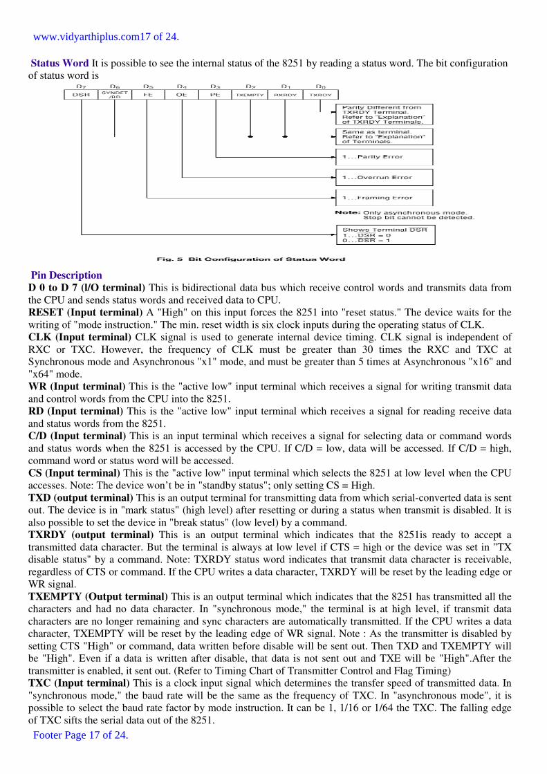
Status Word It is possible to see the internal status of the 8251 by reading a status word. The bit configuration
of status word is
Pin Description
D 0 to D 7 (l/O terminal) This is bidirectional data bus which receive control words and transmits data from
the CPU and sends status words and received data to CPU.
RESET (Input terminal) A "High" on this input forces the 8251 into "reset status." The device waits for the
writing of "mode instruction." The min. reset width is six clock inputs during the operating status of CLK.
CLK (Input terminal) CLK signal is used to generate internal device timing. CLK signal is independent of
RXC or TXC. However, the frequency of CLK must be greater than 30 times the RXC and TXC at
Synchronous mode and Asynchronous "x1" mode, and must be greater than 5 times at Asynchronous "x16" and
"x64" mode.
WR (Input terminal) This is the "active low" input terminal which receives a signal for writing transmit data
and control words from the CPU into the 8251.
RD (Input terminal) This is the "active low" input terminal which receives a signal for reading receive data
and status words from the 8251.
C/D (Input terminal) This is an input terminal which receives a signal for selecting data or command words
and status words when the 8251 is accessed by the CPU. If C/D = low, data will be accessed. If C/D = high,
command word or status word will be accessed.
CS (Input terminal) This is the "active low" input terminal which selects the 8251 at low level when the CPU
accesses. Note: The device won’t be in "standby status"; only setting CS = High.
TXD (output terminal) This is an output terminal for transmitting data from which serial-converted data is sent
out. The device is in "mark status" (high level) after resetting or during a status when transmit is disabled. It is
also possible to set the device in "break status" (low level) by a command.
TXRDY (output terminal) This is an output terminal which indicates that the 8251is ready to accept a
transmitted data character. But the terminal is always at low level if CTS = high or the device was set in "TX
disable status" by a command. Note: TXRDY status word indicates that transmit data character is receivable,
regardless of CTS or command. If the CPU writes a data character, TXRDY will be reset by the leading edge or
WR signal.
TXEMPTY (Output terminal) This is an output terminal which indicates that the 8251 has transmitted all the
characters and had no data character. In "synchronous mode," the terminal is at high level, if transmit data
characters are no longer remaining and sync characters are automatically transmitted. If the CPU writes a data
character, TXEMPTY will be reset by the leading edge of WR signal. Note : As the transmitter is disabled by
setting CTS "High" or command, data written before disable will be sent out. Then TXD and TXEMPTY will
be "High". Even if a data is written after disable, that data is not sent out and TXE will be "High".After the
transmitter is enabled, it sent out. (Refer to Timing Chart of Transmitter Control and Flag Timing)
TXC (Input terminal) This is a clock input signal which determines the transfer speed of transmitted data. In
"synchronous mode," the baud rate will be the same as the frequency of TXC. In "asynchronous mode", it is
possible to select the baud rate factor by mode instruction. It can be 1, 1/16 or 1/64 the TXC. The falling edge
of TXC sifts the serial data out of the 8251.
www.vidyarthiplus.com17 of 24.
Footer Page 17 of 24.

RXD (input terminal) This is a terminal which receives serial data.
RXRDY (Output terminal) This is a terminal which indicates that the 8251 contains a character that is ready
to READ. If the CPU reads a data character, RXRDY will be reset by the leading edge of RD signal. Unless the
CPU reads a data character before the next one is received completely, the preceding data will be lost. In such a
case, an overrun error flag status word will be set.
RXC (Input terminal) This is a clock input signal which determines the transfer speed of received data. In
"synchronous mode," the baud rate is the same as the frequency of RXC. In "asynchronous mode," it is possible
to select the baud rate factor by mode instruction. It can be 1, 1/16, 1/64 the RXC.
SYNDET/BD (Input or output terminal) This is a terminal whose function changes according to mode. In
"internal synchronous mode." this terminal is at high level, if sync characters are received and synchronized. If
a status word is read, the terminal will be reset. In "external synchronous mode, "this is an input terminal. A
"High" on this input forces the 8251 to start receiving data characters.
In "asynchronous mode," this is an output terminal which generates "high level"output upon the detection of a
"break" character if receiver data contains a "low-level" space between the stop bits of two continuous
characters. The terminal will be reset, if RXD is at high level. After Reset is active, the terminal will be output
at low level.
DSR (Input terminal) This is an input port for MODEM interface. The input status of the terminal can be
recognized by the CPU reading status words.
DTR (Output terminal) This is an output port for MODEM interface. It is possible to set the status of DTR by
a command.
CTS (Input terminal) This is an input terminal for MODEM interface which is used for controlling a transmit
circuit. The terminal controls data transmission if the device is set in "TX Enable" status by a command. Data is
transmitable if the terminal is at low level.
RTS (Output terminal) This is an output port for MODEM interface. It is possible to set the status RTS by a
command.
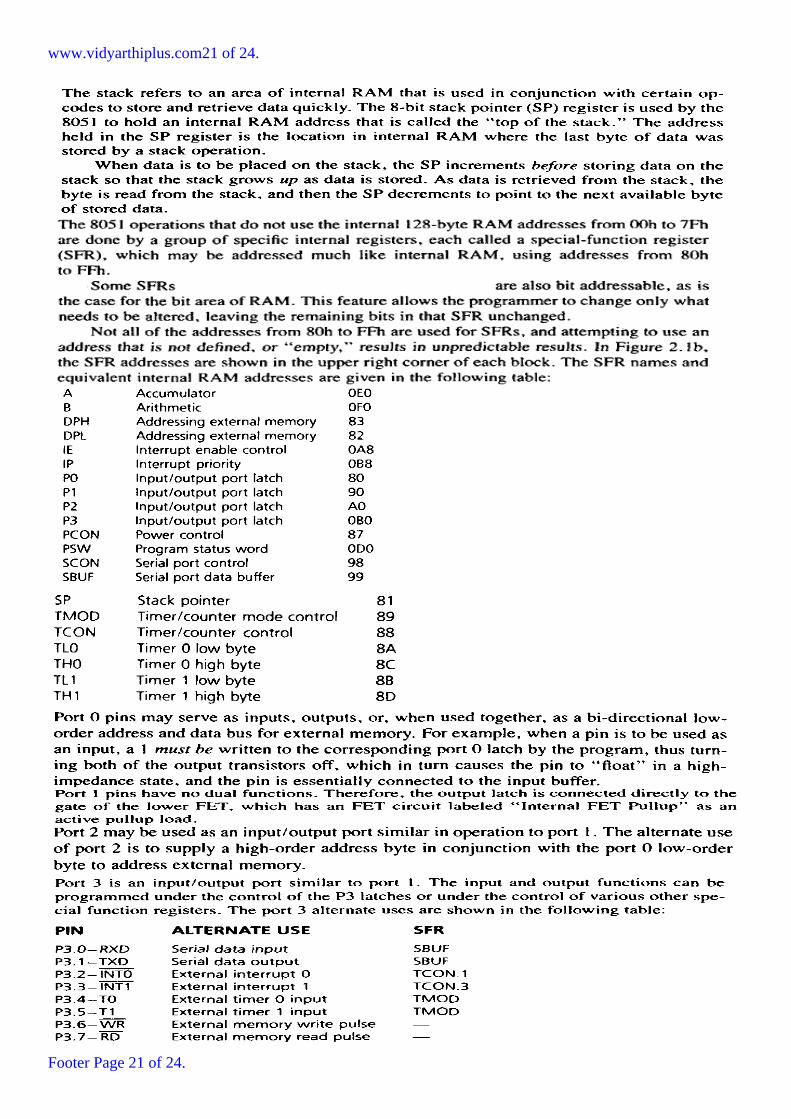
14. a. Explain the architecture of 8051 micro controller and its addressing modes.
www.vidyarthiplus.com18 of 24.
Footer Page 18 of 24.

www.vidyarthiplus.com19 of 24.
Footer Page 19 of 24.

www.vidyarthiplus.com20 of 24.
Footer Page 20 of 24.
www.vidyarthiplus.com21 of 24.
Footer Page 21 of 24.

b. Write short notes on i. Operating modes in Timer ii. Serial Communication.
Timer
Serial communication
www.vidyarthiplus.com22 of 24.
Footer Page 22 of 24.

15. a. Explain the instruction set of 8051. Explain microcontroller based stepper motor control.
The data Transfer instructions are MOV, MOVX, MOVC, PUSH, POP, XCH, XCHD
The logical instructions are AND, OR, NOT, XOR,
The rotate operators are RR, RRC, RL, RLC, SWAP, CLR, CPL
Arithmetic operators are ADD, ADDC, INC, DEC, SUBB, MUL, DIV, DA
Jump and Call instructions are JC, JNC, JB, JNB, JBC, JZ, JNZ, JMP, AJMP, SJMP, LJMP, NOP, DJMP,
ACALL, LCALL, RET
Stepper Motor
A stepper motor is a brushless, synchronous electric motor that converts digital pulses into mechanical shaft
rotation. Every revolution of the stepper motor is divided into a discrete number of steps, and the motor must be
sent a separate pulse for each step. INTERFACING STEPPER MOTOR
To interface the Stepper Motor to microcontroller. As you can see the stepper motor is connected with
Microcontroller output port pins through a ULN2803A array. So when the microcontroller is giving pulses with
particular frequency to ls293A, the motor is rotated in clockwise or anticlockwise.
INTERFACING STEPPER MOTOR WITH 8051
www.vidyarthiplus.com23 of 24.
Footer Page 23 of 24.
We now want to control a stepper motor in 8051 trainer kit. It works by turning ON & OFF a four I/O port lines
generating at a particular frequency.
The 8051 trainer kit has three numbers of I/O port connectors, connected with I/O Port lines (P1.0 – P1.7),(p3.0
– p3.7) to rotate the stepper motor. Ls293d is used as a driver for port I/O lines, drivers output connected to
stepper motor, connector provided for external power supply if needed.
b. Write a simple 8051 assembly language program for performing four basic arithmetic operation on
two data.
MOV A, 08
ADD A, 04
MOV DPTR, #ADD
MOVX @DPTR, A
SUBB A, 08
MOV DPTR, #ADD
MOVX @DPTR, A
MOV B, 04
MUL AB
MOVX DPTR, #ADD
MOVX DPTR, A
INR DPTR
MOV A, B
MOVX DPTR, A
MOV B, 04
DIV AB
MOVX DPTR, #ADD
MOVX DPTR, A
INR DPTR
MOV A,B
MOVX DPTR, A
SJUMP HLT
www.vidyarthiplus.com24 of 24.
Footer Page 24 of 24.


![[4173]-101 - Vidyarthiplus](https://img.pdfslide.us/doc/110x75/61d6e0e3f9ec18156175b586/4173-101-vidyarthiplus.jpg)