Embed Size (px)
Citation preview

Performance variations due to layout-dependent stress in
VLSI circuits
A THESIS
SUBMITTED TO THE FACULTY OF THE GRADUATE SCHOOL
OF THE UNIVERSITY OF MINNESOTA
BY
Sravan Kumar Marella
IN PARTIAL FULFILLMENT OF THE REQUIREMENTS
FOR THE DEGREE OF
Doctor of Philosophy
Sachin S. Sapatnekar
May, 2015
© Sravan Kumar Marella 2015
ALL RIGHTS RESERVED

Acknowledgements
I would like to express my deep gratitude to my advisor Prof. Sachin Sapatnekar for being
the driving force behind this doctoral thesis and for his constant support and encouragement
during my PhD. Prof. Sachin’s persistent efforts have helped me sustain the momentum towards
completing my PhD. I am indebted to him for considering me as his student and for shaping me
as a better researcher. I would also like to thank him for the time and attention given for my
thesis in providing constructive feedback and useful critique. His wide range of accomplishments
coupled with his technical expertise are a great source of inspiration. It is indeed a privilege
to work with one of the finest engineers and a highly regarded professor in the field of VLSI
computer aided design.
I have gained a lot of valuable experience by observing his problem solving skills and his
ability to delineate complex ideas into simple words. I strongly believe my learnings under his
tutelage will go a long way in shaping my future career. Critical thinking, thoroughness, and
attention to detail are some the key skills I have garnered during my association with him. His
unflinching dedication towards shaping future researchers is commendable and he has always
provided me with the right opportunities that helped me grow professionally. In spite of his
various achievements, he is a very grounded person. Personally he is very friendly, helpful, and
considerate towards others. His attitudes towards life and career are truly worth emulating.
Furthermore, I would like to thank my committee members Prof. Chris Kim, Prof. Perry
Leo, and Prof. Ted Higman, for going through my thesis and for their feedback. I would also
like to thank them for the individual discussions during the course of my PhD work which
helped me progress. I am grateful to the university, ECE department, Semiconductor Research
Corporation (SRC), and National Science Foundation (NSF) for the resources and financial
support. I would like to thank the support staff of ECE department for ensuring our systems
run properly with the right software and for fixing problems promptly. I express my thanks to
Minnesota Supercomputing Institute for providing the resources and timely support to perform
valuable large-scale simulations for my work.
I would like to thank my professors at NIT, Warangal, Prof. K. S. R. Krishna Prasad, and
i

Prof. N. S. Murthy for introducing me to the field of VLSI and for encouraging me to pursue
PhD. I would like to extend my thanks to my colleagues at Intel, Bangalore for encouraging me
pursue academics. I would also like to acknowledge my close friend Praveen Salihundam, my
batch-mate at NIT, Warangal and later my colleague at Intel, for encouraging me to apply for
PhD.
A PhD life is not complete without enthusiastic and cheerful lab-mates. I have made great
friends with Vivek, Sriharsha, Deepashree, Zhaoxin, Meghna, and Farhana. It is great to have
fellow team members who share similar aspirations and the conversations with them brought new
perspectives to life and work. I would also like to thank Pingqiang and Saket for sharing several
useful tips on latex writing and on successful PhD completion. I will cherish the camaraderie
and friendship with them.
To do a PhD, it is important to have highly supportive family members. I would not have
been at this stage without the support and love of my parents – Dr. Bhaskar Ramalingeswara
Sarma and Sumitra. They are my first teachers and instilled the confidence in me to achieve
bigger goals in life through their dedicated efforts. I am deeply indebted to them for giving me
the freedom to pursue my passion without financial worries. My younger sister Dr. Supriya
has also been a constant source of encouragement and her wit and humour kept me sane in all
these years. It is fortunate to have understanding in-laws who support your decision to pursue
academics. Special thanks to my dear wife Sujata, whose love and affection has made this journey
a memorable experience. I am truly grateful for her constant encouragement, understanding,
and unflinching support during my PhD.
ii

Dedication
To my parents, my wife, and my son.
iii
Abstract
Layout-dependent stress is a significant source of variability in advanced VLSI technolo-
gies that impacts circuit performance. Mechanical stress affects transistor electrical parameters
mobility and threshold voltage due to piezoresistivity and stress-induced band deformation, re-
spectively. Unintentional sources of mechanical stress and intentional stress variability cause
device performance to depend upon the underlying layout topology and its location in the lay-
out. Advanced packaging technologies have exacerbated this class of variability by introducing
new set of unintentional stresses in the layout. Consequently, circuit performance becomes
highly placement dependent. The traditional paradigm of using pessimistic margins to account
for variations can make meeting stringent design specifications a daunting task. Thus, it is
imperative to capture the effects of layout dependent stress during circuit analysis. Evaluat-
ing circuit performance involves modeling the stress distributions in the layout accurately and
translating the mechanical abstraction of the layout to circuit-level abstraction. This thesis
develops scalable techniques to characterize the layout-dependent stress effects to quantify the
ensuing circuit-level variations in path delays and leakage power. Based on this analysis, layout
optimization strategies are derived.
In 3D-ICs, through silicon vias (TSVs) introduce unintentional thermally-induced stress in
the layout, which results in placement dependent circuit performance variations. Thermal-stress
effects are coupled with other temperature effects on transistor parameters that are seen even
in the absence of TSVs. Analytical models are developed to holistically represent the effect of
thermally-induced variations on circuit timing and leakage power consumption. A biaxial stress
model is built, based on a superposition of 2D axisymmetric and Boussinesq-type elasticity
models. The computed stresses and strains are then employed to evaluate changes in transistor
mobility, saturation velocity, and threshold voltage. The electrical variations are translated into
gate-level delay and leakage power calculations, which are then elevated to circuit-level analysis
to thoroughly evaluate the variations in circuit performance induced by TSV stress. Finally,
layout guidelines are presented that optimize circuit delays in 3D-ICs.
Thermal stresses from shallow trench isolation (STI) are another major source of uninten-
tional stress that affect bulk planar transistors in conventional and 3D integrated circuits. STI is
employed to electrically isolate transistors and the amount of STI surrounding an active region
depends upon the location of the neighboring transistors in the layout. An analytical model
based on inclusion theory in micromechanics is employed to accurately estimate the biaxial
stresses and the strains induced in the active region by the surrounding STI in the layout. The
induced changes in mobility and threshold voltage changes are computed at the transistor level
iv
and then propagated to the gate and circuit levels to predict circuit-level delay and leakage
power for a given placement. For 3D-ICs, the combined effects of STI and TSV are evaluated.
In bulk technologies, intentional source/drain stressors are used to enhance transistor perfor-
mance. In FinFET technologies, these stressors lose their effectiveness with reducing contacted
gate pitch. Moreover, owing to the three dimensional nature of the FinFETs, the beneficial
stress relaxes along the free-edges of standard cell layouts. Thus, the magnitudes of engineered
mechanical stress depend upon the underlying layout topology. To improve circuit performance,
a dual gate pitch technique is proposed, where standard cells with twice the gate pitch are
selectively used on the gates of the circuit critical paths, at minimal area and power costs. A
stress-aware library characterization is performed for FinFET-based standard cells by obtaining
stress distributions using finite element simulations on a subset of structures. The stresses are
then employed to create look-up tables for mobility multipliers and threshold voltage shifts, for
subsequent performance characterization of FinFET-based standard cells. Finally, a circuit de-
lay optimizer is applied using the dual gate pitch approach and is compared with an alternative
gate sizing approach in 14nm/10nm/7nm technologies. Using a combination of gate sizing and
the dual gate pitch approach, it is shown that the power delay product of FinFET-based circuits
can be improved.
v

Contents
Acknowledgements i
Dedication iii
Abstract iv
List of Tables iv
List of Figures vi
1 Introduction 1
1.1 Stress effects in CMOS circuits . . . . . . . . . . . . . . . . . . . . . . . . . . . . 2
1.1.1 Sources of intentional mechanical stress . . . . . . . . . . . . . . . . . . . 4
1.1.2 Sources of unintentional stress . . . . . . . . . . . . . . . . . . . . . . . . 6
1.2 Goals of this thesis . . . . . . . . . . . . . . . . . . . . . . . . . . . . . . . . . . . 7
1.3 Thesis organization . . . . . . . . . . . . . . . . . . . . . . . . . . . . . . . . . . . 9
2 Stress and electrical modeling 10
2.1 Stress modeling . . . . . . . . . . . . . . . . . . . . . . . . . . . . . . . . . . . . . 10
2.1.1 Definitions and notations . . . . . . . . . . . . . . . . . . . . . . . . . . . 10
2.1.2 Governing equations of elasticity . . . . . . . . . . . . . . . . . . . . . . . 12
2.1.3 Analytical solution approaches . . . . . . . . . . . . . . . . . . . . . . . . 14
2.1.4 Finite-element-based solutions . . . . . . . . . . . . . . . . . . . . . . . . 15
2.1.5 Comparison of analytical techniques and FEM . . . . . . . . . . . . . . . 16
2.2 An appropriate coordinate system for VLSI circuits . . . . . . . . . . . . . . . . . 17
2.3 Electrical variation modeling . . . . . . . . . . . . . . . . . . . . . . . . . . . . . 18
2.3.1 Transistor low-field mobility variation with stress . . . . . . . . . . . . . . 19
2.3.2 Saturation velocity variation with mechanical stress . . . . . . . . . . . . 20
i

2.3.3 Threshold voltage variation due to mechanical stress . . . . . . . . . . . . 21
2.4 Gate-level delay and leakage power models . . . . . . . . . . . . . . . . . . . . . . 22
2.4.1 Gate-level delay estimation . . . . . . . . . . . . . . . . . . . . . . . . . . 23
2.4.2 Gate-level leakage power estimation . . . . . . . . . . . . . . . . . . . . . 23
3 Holistic analysis of circuit performance variations under temperature and
TSV-induced stress effects 26
3.1 Introduction . . . . . . . . . . . . . . . . . . . . . . . . . . . . . . . . . . . . . . . 27
3.2 Stress modeling . . . . . . . . . . . . . . . . . . . . . . . . . . . . . . . . . . . . . 29
3.2.1 Overview of our TSV stress solution . . . . . . . . . . . . . . . . . . . . . 30
3.2.2 2D-axisymmetric solution . . . . . . . . . . . . . . . . . . . . . . . . . . . 30
3.2.3 Solving the Boussinesq problem . . . . . . . . . . . . . . . . . . . . . . . . 32
3.3 Application to integrated circuits . . . . . . . . . . . . . . . . . . . . . . . . . . . 34
3.3.1 Stress in Cartesian coordinate systems . . . . . . . . . . . . . . . . . . . . 35
3.3.2 Impact of the crystal orientation . . . . . . . . . . . . . . . . . . . . . . . 37
3.3.3 Comparison with finite element simulation . . . . . . . . . . . . . . . . . . 38
3.4 Effects of stress on electrical parameters . . . . . . . . . . . . . . . . . . . . . . . 39
3.4.1 TSV-induced mobility variations. . . . . . . . . . . . . . . . . . . . . . . . 39
3.4.2 TSV-induced threshold voltage variations . . . . . . . . . . . . . . . . . . 41
3.5 Timing analysis under electrical variations . . . . . . . . . . . . . . . . . . . . . . 42
3.5.1 Delay dependence on temperature . . . . . . . . . . . . . . . . . . . . . . 43
3.5.2 Gate characterization . . . . . . . . . . . . . . . . . . . . . . . . . . . . . 43
3.5.3 Timing analysis framework . . . . . . . . . . . . . . . . . . . . . . . . . . 44
3.6 Results . . . . . . . . . . . . . . . . . . . . . . . . . . . . . . . . . . . . . . . . . . 45
3.6.1 Gate delay comparison: Analytical solution vs. FEA . . . . . . . . . . . . 45
3.6.2 Effect of TSV-induced stress on circuit path delays. . . . . . . . . . . . . 46
3.6.3 TSV-induced stress effects on leakage power . . . . . . . . . . . . . . . . . 52
3.7 Conclusion . . . . . . . . . . . . . . . . . . . . . . . . . . . . . . . . . . . . . . . 52
4 Impact of shallow trench isolation on circuit performance 54
4.1 Introduction . . . . . . . . . . . . . . . . . . . . . . . . . . . . . . . . . . . . . . . 55
4.2 STI-induced stress modeling . . . . . . . . . . . . . . . . . . . . . . . . . . . . . . 57
4.2.1 The inclusion problem in micromechanics . . . . . . . . . . . . . . . . . . 57
4.2.2 Galerkin-vector-function-based stress formulation . . . . . . . . . . . . . . 59
4.2.3 Comparison with the finite element method . . . . . . . . . . . . . . . . . 62
4.3 Electrical effects of STI-induced stress . . . . . . . . . . . . . . . . . . . . . . . . 64
4.3.1 Variation of mobility with stress . . . . . . . . . . . . . . . . . . . . . . . 64
ii

4.3.2 Variation of threshold voltage with stress . . . . . . . . . . . . . . . . . . 66
4.4 Circuit performance evaluation . . . . . . . . . . . . . . . . . . . . . . . . . . . . 66
4.5 Results . . . . . . . . . . . . . . . . . . . . . . . . . . . . . . . . . . . . . . . . . . 68
4.5.1 STI effects in planar integrated circuits . . . . . . . . . . . . . . . . . . . 68
4.5.2 Unintentional stress effects in 3D-ICs . . . . . . . . . . . . . . . . . . . . . 71
4.6 Conclusion . . . . . . . . . . . . . . . . . . . . . . . . . . . . . . . . . . . . . . . 72
5 Optimization of FinFET-based circuits using a dual gate pitch technique 74
5.1 Introduction . . . . . . . . . . . . . . . . . . . . . . . . . . . . . . . . . . . . . . . 75
5.2 FinFET parameters and stressors . . . . . . . . . . . . . . . . . . . . . . . . . . . 77
5.2.1 FinFET structure and layout . . . . . . . . . . . . . . . . . . . . . . . . . 77
5.2.2 Intentional stressors . . . . . . . . . . . . . . . . . . . . . . . . . . . . . . 78
5.3 FinFET stress modeling and characterization . . . . . . . . . . . . . . . . . . . . 79
5.3.1 Stress modeling . . . . . . . . . . . . . . . . . . . . . . . . . . . . . . . . . 79
5.3.2 Simulation of stress relaxation . . . . . . . . . . . . . . . . . . . . . . . . 80
5.4 Stress-aware standard cell characterization . . . . . . . . . . . . . . . . . . . . . . 82
5.4.1 Obtaining mobility multipliers and threshold voltage shifts . . . . . . . . 82
5.4.2 Library characterization . . . . . . . . . . . . . . . . . . . . . . . . . . . . 84
5.5 Results . . . . . . . . . . . . . . . . . . . . . . . . . . . . . . . . . . . . . . . . . . 85
5.5.1 Comparison of layout topologies . . . . . . . . . . . . . . . . . . . . . . . 85
5.5.2 Timing optimization framework . . . . . . . . . . . . . . . . . . . . . . . . 87
5.5.3 Circuit-level optimization with dual gate pitches . . . . . . . . . . . . . . 88
5.6 Conclusions . . . . . . . . . . . . . . . . . . . . . . . . . . . . . . . . . . . . . . . 94
6 Conclusions 95
References 97
Appendix A. Tables of physical constants 106
iii

List of Tables
3.1 Closed-form expressions for TSV-induced stress components . . . . . . . . . . . . 36
3.2 Characteristics of 45nm IWLS 2005 circuits with TSVs . . . . . . . . . . . . . . . 47
3.3 Comparison of critical path delay of circuits without and with TSV + BCB
liner effects . . . . . . . . . . . . . . . . . . . . . . . . . . . . . . . . . . . . . . . 48
3.4 Critical path delay of circuits with TSV + SiO2 liner effects . . . . . . . . . . 48
3.5 Delay changes in the TSV 5 7 circuits with TSV + BCB liner . . . . . . . . . 49
3.6 Minimum path delay of TSV 5 7 circuits with TSV + BCB liner effects . . . 51
3.7 Leakage power of TSV 5 7 circuits . . . . . . . . . . . . . . . . . . . . . . . . . . 52
4.1 Closed-form expressions for STI-induced stress and strain tensor components . . 61
4.2 Delay comparison between FEM and analytical models . . . . . . . . . . . . . . . 64
4.3 Characteristics of 45nm IWLS 2005 circuits . . . . . . . . . . . . . . . . . . . . . 69
4.4 Comparison of delay and leakage power under STI in planar ICs . . . . . . . . . 69
4.5 Comparison of delay and leakage power under STI+TSV effects in 3D-ICs . . . . 72
5.1 FinFET parameters . . . . . . . . . . . . . . . . . . . . . . . . . . . . . . . . . . 78
5.2 Delay and leakage power of 14nm NAND2 cells. . . . . . . . . . . . . . . . . . . . 88
5.3 Circuit optimization results using conventional gate sizing and dual gate pitch
techniques for 14nm technology . . . . . . . . . . . . . . . . . . . . . . . . . . . . 89
5.4 Circuit optimization results using conventional gate sizing and dual gate pitch
techniques for 10nm technology . . . . . . . . . . . . . . . . . . . . . . . . . . . . 89
5.5 Circuit optimization results using conventional gate sizing and dual gate pitch
techniques for 7nm technology . . . . . . . . . . . . . . . . . . . . . . . . . . . . 90
5.6 Circuit optimization results using conventional gate sizing and dual gate pitch
techniques for 14nm technology with tensile STI stress . . . . . . . . . . . . . . . 92
5.7 Circuit optimization results using conventional gate sizing and dual gate pitch
techniques for 10nm technology with tensile STI stress . . . . . . . . . . . . . . . 93
5.8 Circuit optimization results using conventional gate sizing and dual gate pitch
techniques for 7nm technology with tensile STI stress . . . . . . . . . . . . . . . 93
iv

A.1 Mechanical parameters for stress computation . . . . . . . . . . . . . . . . . . . . 106
A.2 Bulk piezoresistivity coefficients (x10−12 Pa−1) in (100) Si [1] . . . . . . . . . . . 106
A.3 Band edge deformation potential constants [2] . . . . . . . . . . . . . . . . . . . . 106
A.4 FinFET piezoresitivity coeffs. in (100) Si [3] . . . . . . . . . . . . . . . . . . . . . 107
v

List of Figures
1.1 Beneficial stress orientations for (a) PMOS and (b) NMOS transistors. The colors
corresponding to longitudinal, transverse, and vertical directions are purple, or-
ange, and blue. Arrows pointing inward (outward) indicate compressive (tensile)
stress. . . . . . . . . . . . . . . . . . . . . . . . . . . . . . . . . . . . . . . . . . . 2
1.2 Comparison of bulk planar transistor and bulk FinFET. The gate oxide is shown
in yellow regions. . . . . . . . . . . . . . . . . . . . . . . . . . . . . . . . . . . . . 3
1.3 A representative 3D-IC with through silicon vias [4]. . . . . . . . . . . . . . . . . 4
1.4 Intentional stressors in the layout. Arrows pointing towards (away from) each
other or downward (upward) indicate compressive (tensile) stress. The yellow
region is the gate oxide. . . . . . . . . . . . . . . . . . . . . . . . . . . . . . . . . 4
2.1 Representation of stress tensor components in Cartesian coordinate system. . . . 12
2.2 (a) Miller indices (b) Coordinate axes in (100) Si with a wafer flat orthogonal to
the [110] orientation. The transistor channel here is perpendicular to the [110]
axis i.e., φ′ = π/2. . . . . . . . . . . . . . . . . . . . . . . . . . . . . . . . . . . . 17
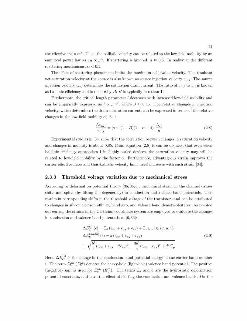
2.3 Representative NAND2 gate. . . . . . . . . . . . . . . . . . . . . . . . . . . . . . 24
2.4 Total leakage power variation with threshold voltage shifts in (a) NMOS transis-
tors (b) PMOS transistors of a 45nm Nangate [5] NAND2 gate. . . . . . . . . . . 24
3.1 Delay dependence of benchmarks (a) ac97 ctrl and (b) usb funct for the cases
where TSV effects are ignored and taken into account. . . . . . . . . . . . . . . . 27
3.2 Axisymmetric geometry of TSV (blue) surrounded by thin liner (yellow) and
encompassed by infinite silicon (green). The z-axis is normal to the plane of the
paper. . . . . . . . . . . . . . . . . . . . . . . . . . . . . . . . . . . . . . . . . . . 31
3.3 Boussinesq problem for surface uniform normal pressure acting on (a) circular
region (TSV region) of area πa2 (b) circular ring-shaped region (liner region) of
area π(b2 − a2). . . . . . . . . . . . . . . . . . . . . . . . . . . . . . . . . . . . . . 34
3.4 Stress contour fields in the [110]-[110] axes. (a) σx′x′ stress contour field. (b) τx′y′
stress contour field. . . . . . . . . . . . . . . . . . . . . . . . . . . . . . . . . . . . 37
vi

3.5 Comparison of (a) σrr and (b) σθθ between the analytical and the FEA models.
Here TSV edge = 2.5µm, liner edge = 2.625µm, and KOZ edge = 3.5µm. . . . . 38
3.6 Mobility variation comparison in uniaxial and biaxial formulations with distance
along (a) y′-axis (b) x-axis. Here TSV edge = 2.5µm, liner edge = 2.625µm, and
KOZ edge = 3.5µm. . . . . . . . . . . . . . . . . . . . . . . . . . . . . . . . . . . 40
3.7 TSV-induced threshold voltage variation in (a) PMOS transistor (b) NMOS tran-
sistor. Here TSV edge = 2.5µm, liner edge = 2.625µm, and KOZ edge = 3.5µm. 42
3.8 Contours of rise time difference of NAND2 gate around a TSV with (a) BCB liner
and (b) SiO2 liner. . . . . . . . . . . . . . . . . . . . . . . . . . . . . . . . . . . . 45
3.9 FO4 rise delay variation of a NAND2 gate with different TSV diameters. The
NAND2 gate is at a distance d from the KOZ edge. . . . . . . . . . . . . . . . . . 46
3.10 Delay changes for benchmark spi (a) PMOS ∆Delay map (b) NMOS ∆Delay map. 50
4.1 A segment of a circuit layout showing how the STI in adjacent cells, or in gaps
between cells, imply that the shape of an STI region depends on the layout of
neighboring cells. . . . . . . . . . . . . . . . . . . . . . . . . . . . . . . . . . . . . 55
4.2 (a) A general inclusion in half-space. (b) STI as a cuboidal inclusion. . . . . . . . 58
4.3 An irregular shaped active region in STI. The STI is fragmented into smaller
cuboids (rectangles in 2D) around the active regions. . . . . . . . . . . . . . . . . 63
4.4 Solid [dashed] lines showing our [FEM] model. (a) σx′x′ (b) σy′y′ . . . . . . . . . . 63
4.5 Contours of (a) PMOS mobility variations (b) NMOS mobility variations as a
function of longitudinal and transverse STI in the layout. Dense layout regions
correspond to lower-left corner and sparse layout regions correspond to upper-
right corner. . . . . . . . . . . . . . . . . . . . . . . . . . . . . . . . . . . . . . . . 65
4.6 Contours of STI-induced threshold voltage shifts in (a) PMOS transistors (b)
NMOS transistors a function of longitudinal and transverse STI in the layout.
Dense layout regions correspond to lower-left corner and sparse layout regions
correspond to upper-right corner. . . . . . . . . . . . . . . . . . . . . . . . . . . . 66
5.1 Pull-up/pull-down transistors with nominal and double the gate pitch. . . . . . . 76
5.2 Changes in critical path delay with gate pitch under intentional stress variability
for two benchmark circuits. . . . . . . . . . . . . . . . . . . . . . . . . . . . . . . 76
5.3 (a) Basic FinFET structure (b) Layout of a 4-fin-4-gate cell with dummy poly
(dashed grey) at the ends. . . . . . . . . . . . . . . . . . . . . . . . . . . . . . . . 77
5.4 Average σx′x′ channel stress among all the transistors due to intentional stress in
(a) PMOS and (b) NMOS transistors. The initial STI stress is compressive. Here
1GP and 2GP correspond to 54nm and 108nm, respectively. . . . . . . . . . . . . 81
vii

5.5 (a) Average mobility (b) Average threshold voltage variations over all transistors
in PMOS and NMOS FinFETs. Here 1GP and 2GP correspond to 54nm and
108nm, respectively. . . . . . . . . . . . . . . . . . . . . . . . . . . . . . . . . . . 84
5.6 Layouts of (a) INV X1 (b) INV X2 (sizing) (c) INV X2 2F (multi-fingered layout
with fewer fins) (d) INV X2 ExDummy (extra dummy gates) and (e) INV X1 2GP
with twice the gate pitch. For a gate pitch of 54nm, the corresponding standard
cell widths are: 108nm, 162nm, 162nm, 216nm and 216nm. . . . . . . . . . . . . 86
5.7 Comparison of ring oscillator delays for different inverters under intentional stress
variability. The corresponding number of fingers in INV X1, INV X2, INV X4,
and INV X8 inverters are 1, 2, 4, and 8. The ring-oscillator delays are normalized
to Library 1GP ring-oscillator. . . . . . . . . . . . . . . . . . . . . . . . . . . . . 86
viii

Chapter 1
Introduction
Technology scaling has enabled feature sizes in integrated circuits (ICs) to shrink, thereby pack-
ing more circuitry within the same chip area. In deeply-scaled technologies, process and envi-
ronment variations have become a major concern since they result in perturbations from the
expected chip behavior. The impact of variations must be taken into account and analyzed dur-
ing the circuit design phase: this helps to optimize or tune technology or design parameters to
meet product specifications. During the past two decades, advances in modeling and circuit per-
formance estimation techniques have largely been able to capture the key impact of process- and
enviromentally-induced variations. In this context, several techniques such as statistical static
timing analysis (SSTA), statistical power estimation, and advanced on-chip variation (AOCV)
have been developed to consider the impact of such variations on circuit performance.
Apart from process and environmental variations, layout-dependent stress effects also con-
tribute performance variations in integrated circuits. In earlier technologies, transistor sizes
were large enough that their electrical behavior was independent of the final layout. However,
in highly scaled technologies with smaller geometries, the electrical performance of a transistor
has become increasingly dependent on its context and location in the layout. Unwanted me-
chanical stresses in the layout, as well as unwanted variations in intentional on-chip stresses,
affect transistor electrical properties due to piezoresistivity and electronic band deformation [6].
Stress effects significantly affect design methodologies in modern integrated circuits, which
are built from a precharacterized library of logic gates. These library cells may be instantiated
multiple times in different parts of the final layout, where they experience different stress levels.
Precharacterizing the performance of the logic cells for a performance metric does not account
for these layout-dependent variations. In addition, advanced packaging techniques have further
resulted in proliferation of unwanted sources of mechanical stress, and the variations caused
by mechanical stress effects have become comparable to those from lithography variations [7].
1

2
Thus, it is important to consider the mechanical stress effects early in the design.
1.1 Stress effects in CMOS circuits
To understand the impact of stress on transistor performance, consider the two types of tran-
sistors in a typical CMOS circuit: the N-type and P-type field effect transistors (FETs). The
electrical current in a N-type FET are due to electrons, while current in a P-type FET is due to
holes, which have the opposite polarity. These FETs have four terminals: the source, drain, and
gate and the bulk. The gate terminal controls the formation of a conducting channel between
source and drain regions, and the charge carriers flow from the source to the drain along this
channel. The bulk terminal typically acts as a reference for the gate voltage and is often tied to
the highest voltage potential for P-type FET and the lowest voltage potential for N-type FET.
(a) (b)
Figure 1.1: Beneficial stress orientations for (a) PMOS and (b) NMOS transistors. The colorscorresponding to longitudinal, transverse, and vertical directions are purple, orange, and blue.Arrows pointing inward (outward) indicate compressive (tensile) stress.
The current-carrying capacity is determined by the transistor dimensions, the mobility of
the charge carriers, and the threshold voltage. The transistor mobility determines how fast
charge carriers can travel from source to drain, while the threshold voltage is the minimum
gate potential that needs to be overcome to turn on the transistor. Applied mechanical stress
affects the band structure of the semiconductor material which in turn affects the mobility and
threshold voltage of the transistor. Depending upon the sign and direction of applied stress,
stress may be beneficial or harmful, i.e., improving or degrading transistor mobilities. Positive
valued stress is known as tensile stress which creates a “stretching” effect, while negative valued
stress is known as compressive stress which creates a “squeezing” effect.

3
Fig. 1.1 shows the preferred stress directions for N-type and P-type transistors. The direc-
tion along the transistor channel where current conduction takes place is defined as longitudinal
direction, and within the plane of the channel, the orthogonal direction is known as the trans-
verse direction. The vertical direction corresponds to the perpendicular to the wafer surface.
The mobility of PMOS transistors is improved under compressive stress along longitudinal di-
rection and tensile stress along the transverse and vertical directions. For NMOS transistors,
mobility improves when tensile stress acts along either longitudinal or transverse direction, and
compressive stress acts along the vertical direction. The opposite orientation of stress leads to
mobility degradation. The actual magnitudes of mobility improvements and degradations can
be explained through piezoresistive property of silicon [8] and is due to the combination of stress
from different directions.
Figure 1.2: Comparison of bulk planar transistor and bulk FinFET. The gate oxide is shown inyellow regions.
To overcome the short channel effects that slowed down the rate of scaling in conventional 2D
transistors, transistor architectures have evolved from conventional planar structures to three-
dimensional structures called FinFETs. Fig. 1.2 shows a comparison between conventional
transistor architecture and the FinFET. In FinFET technology, the transistors are raised from
the substrate into structures known as fins. The gate wraps around the transistor channels
from three directions, thus providing better electrostatic control over the channel. The three-
dimensional nature of the transistor architecture result in unwanted variations in engineered
channel stress.
Advanced chip packaging technologies are also responsible for inducing unintentional stress
in silicon. As scaling reaches its physical limits, a new paradigm of vertical scaling has emerged
where several wafers/dies are stacked vertically in a three-dimensional (3D) fashion. Such pack-
aging techniques are known as 3D-IC packaging. Through silicon vias (TSVs) carry signals and
power between different layers of a 3D-IC. Fig. 1.3 shows a 3D-IC package with through silicon

4
Figure 1.3: A representative 3D-IC with through silicon vias [4].
vias. This technique can be extended for multiple dies stacked together. During manufacturing,
mechanical stresses develop in the system due the thermal mismatch between various layers
and constituent materials thereby causing electrical variations in transistors. Thus, it becomes
imperative to consider the contributions of various unintentional stressors on active devices to
accurately analyze the system performance.
1.1.1 Sources of intentional mechanical stress
Figure 1.4: Intentional stressors in the layout. Arrows pointing towards (away from) each otheror downward (upward) indicate compressive (tensile) stress. The yellow region is the gate oxide.
Device and process engineers have exploited the piezoresistive behavior in CMOS transistors
by deliberately introducing stress in the channels using process techniques. While most of the
stress engineering techniques have been introduced for bulk planar transistors, some of them are
scalable to the FinFETs. The sources of intentional stress are summarized as follows: Uniaxial source/drain stressors: The source/drain regions of the CMOS transistors are
recessed and lattice-mismatched alloys are epitaxially grown in the cavities formed [9]. An

5
SiGe alloy with a larger lattice constant than silicon creates beneficial compressive stress
along the channel direction for PMOS transistors [10,11]. For NMOS transistor type, SiC
alloy with a smaller lattice constant than silicon is epitaxially grown in source/drain re-
gions to create a beneficial tensile stress along the channel direction [12]. The source/drain
stressors have also been applied for FinFETs [13, 14]. This technique is the largest con-
tributor for mobility improvements. Dual stress liner: Dielectric nitride films with intrinsic compressive or tensile stress are
grown over the transistor region [15]. While a tensile stress liner is preferred for NMOS
transistors, a compressive stress liner is preferred for PMOS transistors. They rely on
creating beneficial stress from the vertical direction. However, from the 45nm technology
node onwards, their effectiveness was observed to decline [11]. The stress liners have been
shown to be not effective for FinFETs [16, 17]. Stress memorization technique [18]: This technique is used for NMOS transistors alone.
Here a sacrificial compressive stressed liner is grown on NMOS transistors with polysilicon
gate and source/drain regions in amorphous state. The gate and source/drain regions
are crystallized following a rapid thermal annealing step and the capping stress liner is
removed. Even after the stressed capping layer is removed, stress is memorized in the gate
and source/drain regions. The gate creates a compressive stress from vertical direction,
while tensile stress exists in the source/drain regions. The stress memorization technique
has also been demonstrated for FinFETs [19]. Replacement metal gate and gate-last process: This method has been shown to be effec-
tive for bulk planar transistors and FinFETs. In advanced technologies, metal gates are
employed instead of polysilicon gates to improve threshold voltage control [20]. First a
sacrificial polysilicon gate is deposited and subsequent fabrication steps for source/drain
epitaxy and salicidation are completed. Then the polysilicon gate is stripped off thereby
increasing the stress transferred into the channels [11]. Subsequently, the metal gate is
deposited in the gate terminal region. Using certain process conditions the metal gate
can be incorporated with tensile or compressive strain which acts vertically on the chan-
nels [21,22]. A metal gate with compressive stress is preferred for NMOS transistors, while
a metal gate with tensile stress is preferred for PMOS transitors. Source/drain contact stress: Tensile stress can similarly incorporated in the metal contacts
over source/drain regions of an NMOS transistor [11]. The metal contacts are deposited
by creating trenches in source/drain regions. However, the effectiveness of this technique
is diminishing in sub-45nm technologies, which use raised source/drain regions to reduce
source/drain resistance.

6
In an ideal scenario, all the transistors are required to have identical mobility improvements.
However, intentional stress also undergoes variation depending upon layout parameters. In
particular, the source/drain stressors in bulk planar transistors and FinFETs show dependence
on gate pitch used in the layout which may vary from technology generations. Additionally, in
FinFETs, due to the three dimensional nature of the structure, the engineered stress relaxes
along these facets, thus weakening the efficacy of intentional stressors. The magnitudes of
strain engineered into the channels depend upon the layout topology. Thus while evaluating
the circuit performance of FinFET-based circuits, the underlying layout topology must be taken
into account.
1.1.2 Sources of unintentional stress
In addition to variations in intentional stressors, unintentional stress in the layout interferes with
the engineered intrinsic stress and causes placement-dependent electrical parameter variations.
The unintentional sources of stress can mainly be attributed to the thermal mismatch of the
various materials used during integrated circuit manufacturing. Moreover, integrated circuits
undergo several thermal cycles at elevated temperatures during multiple process steps. The
coefficient of thermal expansion (CTE) of a material determines how fast a material can contract
or shrink with decreasing or increasing temperature. Two major sources of unintentional stress
that lie in proximity of the transistors in integrated circuits are summarized as follows:
Shallow-trench isolation or STI: Shallow trench isolation (STI), which is used to isolate transis-
tors in the layout, is the most commonly found source of unintentional stress in the layout. The
STI is made up of SiO2 whose CTE differs with that of silicon. STI in the layout surrounds the
active transistor regions and can occur in a myriad of shapes depending upon the neighbouring
transistors in the layout. A representative STI is shown in Fig. 1.4 along with other intentional
stressors in the layout.
Through-silicon-via in 3D-ICs: TSVs are used to make vertical interconnections between stacked
integrated circuits. The TSV is embedded in silicon at an elevated temperature of 250oC and
is made up of copper, whose CTE is higher than that of silicon. In the post-manufacturing
phase, a thermal residual stresses develops in the silicon that is in direct contact with the TSV
structure, thus modulating the mobilities of the transistors in near proximity.
Other sources of unintentional stresses that may affect transistor mobilities are caused by
wafer/die warpage during wafer processing and thinning, flip-chip package bumps, and CTE
mismatch between package substrate and silicon die.

7
1.2 Goals of this thesis
From the discussion in the previous section we can conclude that mechanical stress interacts
with the physics of electronic transport and manifests itself in the form of circuit-level perfor-
mance variations. In other words, unintentional mechanical stresses in the layout interfere with
the normal operation of circuits and cause variations in the performance of a chip. Mechanical
stress effects can be seen as a class of process-design interactions. Two approaches are com-
monly employed in the design community to deal with process-design interactions: rule-based
and model-based approaches [7]. In the rule-based approach, engineers apply layout rules and
pessimistic performance guardbands to account for variations. The rule-based approach [23] is
simple to implement, but it may lead to excessive margining and high overheads that make it
arduous to meet stringent system performance specifications under tight time-to-market sched-
ules. On the other hand, the model-based paradigm quantifies the sources of variations on
circuit performance using modeling techniques. Although modeling may involve a greater de-
gree of complexity, the model-based approach aids in optimizing the design parameters and helps
to reduce excessive pessimism in the design specifications. This thesis takes the model-based
approach to accurately capture the effects of unwanted stress and intentional stress variations
on circuit performance by considering the underlying layout into account. Furthermore, based
on the analysis, layout guidelines and layout optimization techniques are developed.
Capturing the effects of layout-dependent stress on circuit performance involves a translation
from a physics abstraction to a circuit- or layout-level abstraction. The challenges involved are
threefold: Modeling: Mechanical stresses in transistor channels must be accurately modeled under
the layout environment around the transistor. The stresses should then be translated from
the physics regime to a circuit abstraction using appropriate electrical models. Scalable
techniques should be developed to evaluate stress distributions on large layouts. Analysis: The magnitude of stress-induced variation in circuit-level performance metrics
must be quantified. This involves the integration of stress-based models into standard
circuit performance estimation techniques. The primary metrics of concern are worst-
case path delay of the circuit, which determines the chip operating frequency and the
power consumption of the circuit. To estimate the worst-case delay in the circuit, static
timing analysis is used [24] , while leakage power can be estimated using standard power
estimation techniques [25]. Since timing and power analysis are frequently invoked in the
inner loop of circuit optimizers, fast analysis techniques that capture the impact of the
layout-dependent effects are essential.
8 Optimization: Based on the analysis, it is necessary to develop layout or circuit op-
timization techniques that can be woven seamlessly into the design flows of integrated
circuits.
Our goal is to develop scalable computer-aided design techniques to analyze and optimize the
layout-dependent mechanical stress effects on circuit performance. Specifically, we focus on
capturing the performance variations under the following set of mechanical stress effects:
1. TSV-induced stress effects: The residual thermal stress effects due to TSVs in 3D-ICs
impact the nearby transistor’s electrical parameters, namely, the mobility and threshold
voltage. In addition, both the transistor electrical parameters and mechanical stress inde-
pendently dependent on temperature. Thus, it is necessary to capture both temperature
and TSV-induced stress effects together in a single analysis. In Chapter 3, we develop a
scalable analytical stress model to accurately predict the biaxial TSV-induced stress dis-
tributions in transistors by considering their relative positions with respect to TSVs in the
layout. The mechanical stress distributions are then translated to electrical and gate-level
delay metrics using analytical models. A thorough analysis of circuit path delay variations
and leakage power variations are predicted. Finally, we develop layout guidelines that
optimize the delay of the circuits in 3D-ICs.
2. STI-induced stress effects: STI continues to be the most popular choice of transistor
isolation technique in VLSI circuits. STI is present between active transistor regions in
both planar ICs and 3D-ICs. In bulk planar technologies, the ensuing mechanical stress
in transistor channels depends upon the shape of the STI in the immediate vicinity of
the transistor and is determined by the neighboring positions of other transistors in the
layout. However, STI can occur in a variety of shapes for different instances of a given
standard cell in the final circuit layout. In Chapter 4, we develop an analytical stress model
based on techniques in micromechanics to accurately determine the stress in transistors
due to surrounding STI in the layout. The circuit level delay and leakage power variations
are estimated and layout guidelines to optimize delay are derived. Finally, the combined
effects of STI and TSVs are estimated for 3D-ICs.
3. Local stress relaxation in FinFETs: For FinFET-based circuits, due to the three
dimensional structure of the transistors, the engineered stresses undergo stress relaxation
along the free surfaces of the layout. Thus, the magnitude of the engineered stress and
hence the performance improvements depend upon the underlying layout topology in these
circuits. In particular, it is found that the effectiveness of the source/drain stressors
diminish with gate pitch scaling. In Chapter 5, a dual gate pitch technique is proposed,
where selected standard cells on the critical paths of the circuit are replaced with equivalent

9
cells with twice the gate pitch. First, the stress distributions in the FinFET channels are
evaluated using finite element techniques. The stresses are then translated to transistor-
level electrical variations. The transistor level improvements are then integrated into
SPICE simulations during library characterization. Finally, we present a sensitivity-based
circuit optimization technique using the dual gate pitch technique in combination with
conventional gate-sizing approach to improve the circuit performance.
1.3 Thesis organization
The thesis is organized as follows. Chapter 2 introduces the modeling techniques required for
estimating stress distributions, changes in electrical parameters due to applied stress, and for
estimating gate-level performance metrics. Subsequent chapters derive the specific solution
techniques based on the results in Chapter 2. While Chapters 3 and 4 employ analytical stress
modeling techniques for estimating performance variations, Chapter 5 relies on finite element
simulations to predict stress distributions in FinFETs.

Chapter 2
Stress and electrical modeling
This chapter introduces the analytical stress and electrical models used in this work. First
the fundamental equations of elasticity are presented and the solution strategies are discussed.
An appropriate coordinate system, based on Miller indices, is established, within which the
stress distributions are evaluated. Next, the impact of mechanical stress on transistor electrical
properties, such as mobility and threshold voltage, is captured. The fundamental models of
piezoresistivity and deformation potential theory are presented to characterize the changes in
mobility and threshold voltage, respectively, under stress. Finally, gate-level delay and leakage
power are expressed as functions of perturbations to the electrical parameters of individual
transistors in the standard cell using sensitivity-based models. Subsequent chapters draw upon
the basic equations from this chapter to obtain specific solutions for the relevant problems.
2.1 Stress modeling
This section provides the basic equations of elasticity and the solution approaches to determine
the stress state of a system. A qualitative comparison of analytical and finite element techniques
is discussed here, with specific focus on their applicability to problems in integrated circuits.
2.1.1 Definitions and notations
In the theory of linear elasticity, the following terms are frequently used: Stress is defined as applied force per unit area, and physically corresponds to the reac-
tionary internal forces that develop in a body due to applied external forces. The SI unit
of stress is Pascal (Pa).
10

11 Strain is defined as relative change in the dimensions of a body due to applied forces and
is determined by the ratio of the change in dimensions to the original dimension. Thus,
strain is a unit-less quantity. Displacement is defined as the actual change in dimensions of a deformed body due to
applied forces.
It should be noted that every physical deformation of a body that causes a change in the original
shape is associated with a strain. During a natural deformation, such as a free expansion or
contraction due to a change in temperature, there is no stress developed in the body but it does
experience strain. This is known as stress-free strain. Stress develops in the body only when
the natural deformation of the body is constrained by some means.
In integrated circuits, stress may develop when two objects with differing rates of thermal
expansion happen to be in contact. The stress thus developed is known as thermal stress.
Integrated circuits are typically manufactured at elevated temperatures and consists of various
materials with differing coefficient of thermal expansion (CTE). Thus, post-manufacturing, at
room temperatures or typical chip operating temperatures, there is a residual thermal stress due
to the CTE mismatch between materials in the chip.
Applied external forces cause a physical deformation (strain) in materials. In elastic ma-
terials, the internal forces (stress) tend to regain the original shape when the external force is
removed. It has been empirically observed that for small deformations, the stress developed
is proportional to the strain, and this is known as the Hooke’s Law. It should be noted that
Hooke’s Law does not apply to natural deformation of elastic bodies (stress-free strain), since
the body changes from one intrinsic state to another intrinsic state. The constant of proportion-
ality is a physical property of the material and is known as its Young’s Modulus. The stiffer the
material, the higher the magnitude of its Young’s Modulus, and hence greater the stress level
corresponding to a given strain. When a material is stretched or compressed along a certain
direction, there is a corresponding contraction or expansion of the material in the orthogonal
direction so that the volume of the body remains the same. The negative ratio of the strain
in the orthogonal direction to the strain along the direction of the applied force is known as
the Poisson’s ratio of the material. It should be noted that Poisson’s ratio is always a positive
fraction less than one. Beyond a stress level known as the yield point or yielding stress, the stress
and strain are no longer linear and the material ceases to be elastic. The physical body can no
longer regain its original shape and continues to yield to applied forces. This regime is termed as
the plastic regime. When the strain levels continue to increase with applied force, the physical
body reaches a fracture point where atomic bonds are broken and the material fractures.
For the strain levels seen in integrated circuits, silicon and other constituent materials exhibit
the property of elasticity. Furthermore, the materials used integrated circuits, as considered in

12
this work, are assumed to have no discontinuities in their physical structure, and thus are termed
as homogenous. The materials in this work are considered to be isotropic, i.e., they have identical
material properties in all directions.
Figure 2.1: Representation of stress tensor components in Cartesian coordinate system.
The mechanical stress field is represented as a tensor that comprises six unique stress compo-
nents: three normal stresses (σ11, σ22, σ33) and three shearing stresses (τ12, τ23, τ31), where the
subscripts 1, 2, and 3 correspond to the three orthogonal axes in any spatial coordinate system.
The stress components may be compactly represented as σij with i, j ∈ 1, 2, 3. Similarly, the
six strain [three displacement] fields are represented by ǫij [ui] where i ∈ 1, 2, 3. In Cartesian
coordinates, these correspond to the x, y, and z directions, while in cylindrical coordinates the
axes are along radial (r), circumferential (θ), and axial (z) directions. Fig. 2.1 shows the stress
tensor components defined in the Cartesian coordinate system.
Einstein notation In order to express the tensorial equations compactly, we employ Einstein
notation, where repeated indices indicate summation. The following three examples illustrate
the usage:
Example 1: c = aibi =∑N
i=1 aibi denotes single summation with N terms.
Example 2: ci = aijbj =∑M
j=1 aijbj denotes N summations with i ∈ [1, N ].
Example 3: cij = aijklbkl =∑Ok=1
∑Pl=1 aijklbkl denotes N × M summations with i ∈ [1, N ],
and j ∈ [1, M ].
2.1.2 Governing equations of elasticity
The stress state of a system can be fully described by 15 unknowns: six stress components, six
strain components, and three displacement components. The relations between the 15 unknowns
are expressed within 15 equations:
13 6 stress-strain equations (Hooke’s Law):
σij = Cijkl(ǫkl − ǫ∗kl) (2.1) 6 strain-displacement equations:
ǫij =1
2
(
∂ui∂xj
+∂uj∂xi
)
(2.2) 3 force-balance equations:
∂σix1
∂x1+
∂σix2
∂x2+
∂σix3
∂x3+ Bi = 0 (2.3)
Here, i, j, k, l ∈ x1, x2, x3 and Bi is the external body force. The term ǫij corresponds to
the total strain which is a sum of elastic and inelastic part of the strain [26, 27]. The term ǫ∗kl
refers to the inelastic part of the strain which corresponds to thermal mismatch strains, lattice
mismatch strains or any other initial strains. In particular, the thermal mismatch strain is given
by ǫ∗kl = δklα∆T , where δkl is Kronecker’s delta function, α denotes the coefficient of thermal
expansion, ∆T refers to the change in temperature.
The Cijkl elements here represent the components of the stiffness tensor and is a function of
Young’s modulus E and Poisson’s ratio ν of the material. The nonzero components are given
below:
C1111 = C2222 = C3333 =E(1 − ν)
(1 + ν)(1 − 2ν)
C1122 = C2233 = C1133 =Eν
(1 + ν)(1 − 2ν)
C2211 = C3322 = C3311 =Eν
(1 + ν)(1 − 2ν)
C1212 = C3131 = C2323 =E
2(1 + ν)(2.4)
The solution to the governing equations in (2.1), (2.2), and (2.3) depends upon the geometry
and boundary conditions of the mechanical system.
Three-dimensional problems in elasticity can often be reduced to two-dimensional problems
to simplify solution procedures. These are known as plane problems, where displacement and
stress components can be treated independent of one of the axis directions, based on the geom-
etry. For ease of discussion we shall refer to this independent axis direction as the x3-axis and
use cylindrical coordinates to describe the approaches. These plane problems can be solved in
two ways [26]:

14 A plane strain approach is used when the dimensions of a body along the x3-axis is much
larger than the cross-section along the orthogonal axes directions. This makes the dis-
placements and the stresses independent of the x3-direction. Furthermore, ǫix3 = 0 with
i ∈ x1, x2, x3, in the plane strain approach. However, from Hooke’s Law in Equa-
tion (2.1), we can see that σx3x3 = C3311ǫx1 + C3322ǫx2 6= 0. Thus, even when the x3-
dimensional strains are zero, it can be shown that σx3x3 can be nonzero in general due to
the Poisson’s effect of stresses in other directions. A plane stress condition is said to exist when a body is bounded by two parallel planes
(orthogonal to x3-axis) separated by a distance which is smaller compared to the other
dimensions. Here, the stresses and displacements almost remain the same between the
two parallel planes and hence are independent of the x3-direction. Furthermore, in plane
stress problems, σx3x3 = 0 and τix3 = 0 with i ∈ x1, x2. Analogous to the plain strain
approach, from Hooke’s Law, ǫzz can be nonzero in general for a plane stress analysis.
The system of equations can be either solved analytically resulting in closed-form solutions, or
solved numerically using the finite element method (FEM). In this work, we use analytical models
when possible and validate or calibrate the stress distributions thus obtained with those from
FEM to ensure that the analytical model has adequate accuracy. When closed-form solutions
are not readily possible and when the number of possible cases/parameters is fewer in number,
we resort to FEM to ensure accurate stress distributions. Analytical techniques are employed
in Chapter 3 and Chapter 4 to obtain closed-form solutions for TSV and STI/source-drain
stressors, respectively. On the other hand, in Chapter 5, FEM simulations are used to obtain
stress distributions in FinFETs.
2.1.3 Analytical solution approaches
Analytical solutions can be obtained by solving the system of partial differntial equations
in (2.1), (2.2), and (2.3). Closed-form solutions are possible when the system of equations
become homogenous by considering the body forces to be absent. When the body forces
Bi, i ∈ x1, x2, x3, are zero, it can be shown that the displacements or stresses can be rep-
resented in terms of a function Φ that satisfies the relation:
∇4Φ = 0 (2.5)
The solution to the system of elasticity equations can be found in terms of a biharmonic
function, Φ, that satisfies the specified boundary conditions of the system. A biharmonic [har-
monic] function is a function whose fourth [second] order partial derivative is zero. The solution
techniques to obtain closed-form solutions are classified as follows [28, 26, 29]:

15 Direct method: The system of partial differential equations is solved directly using
standard techniques for partial differential equations. The particular solutions depend
upon the specified boundary conditions. Often this method is possible only for simple
geometries. Stress formulation or stress function approach: The stress components in the system
can be expressed as partial derivatives of specific harmonic or biharmonic functions that
satisfy the boundary conditions. Once the stress is known, the other unknowns of the
stress state can be determined from Equations (2.1) and (2.2). The primary limitation of
this method is that the form of the functions that satisfy the boundary conditions must
be correctly guessed. Furthermore, to obtain the displacements, complicated integrations
must be performed, and closed-form solutions may not always be available. Displacement formulation: The displacement is equated to the second partial deriva-
tive of a biharmonic function that satisfies the boundary conditions. Once the displacement
[stress] is known, the other unknowns of the stress state can be determined from Equa-
tions (2.1), (2.2), and (2.3). Compared to stress formulation approach, this method is
relatively flexible since the basic biharmonic functions can be constructed from commonly
used potential functions or can be represented in Fourier series form [28].
In Chapter 3, the stress due to TSVs can be obtained in the cylindrical coordinate system
using the direct method or the stress function approach. On the other hand, stress model-
ing in Chapter 4 employs the displacement formulation approach coupled with principles from
micromechanics.
2.1.4 Finite-element-based solutions
Closed-form solutions can be obtained for simple geometries using analytical models. However,
for more general shapes and complex boundary conditions, the elasticity equations tend to
be intractable and may require complicated mathematical analysis. In such scenarios, FEM
allows the elasticity equations to be solved using numerical methods [26]. First the body is
discretized into subdomains known as elements with special points called nodes. The elements
usually take two-dimensional or three-dimensional polygonal shapes and the nodes correspond
to the corners of the polygon. Approximate solutions are developed for each element in terms
of nodal values. Algebraic equations are then constructed among the nodal values, based on
their physical connectivity and by applying continuity and prescribed boundary conditions. The
algebraic equations are then solved to obtain the required values of the stress distributions. If
the number of elements is sufficiently large, the solution can be considered to be accurate. In

16
this thesis, we use the ABAQUS [30] finite element package for obtaining stress distributions in
silicon as shown in subsequent chapters.
2.1.5 Comparison of analytical techniques and FEM
Closed-form solutions for boundary value problems in elasticity often require certain assumptions
on the geometry, such as assuming that the body is infinite or semi-infinite, to simplify the
solution procedures. On the other hand, FEM does not require such assumptions. FEM solves
the system of elasticity equations numerically by dividing the physical system into several nodes
or meshes. FEM can capture the finite dimensions of a physical problem and the accuracy
depends upon how finely the object is divided into elements. Moreover, FE simulations can also
capture the microstructures of the mechanical system accurately, while the usage of analytical
closed-form models require ignoring or omitting certain microstructures.
Analytical models lend themselves to faster computation, so that stress distributions can
be obtained in the order of few microseconds, while FEM simulations are compute-intensive
since the stress equations must be solved numerically at a large number of nodes. The run
time of a typically FE simulation could range from few seconds to several hours, depending
upon the problem size and accuracy requirements. This computational cost typically makes FE
simulations prohibitive for use in the inner loop of an optimizer.
An alternative semi-analytical approach is to precharacterize the stress distributions for
an integrated circuit problem and store the results in look-up tables. However, the storage
overhead in using look-up tables increases exponentially with the number of input parameters.
For example, both mechanical stress and circuit electrical parameters such as mobility and
threshold voltage independently depend upon temperature. When solving a thermal stress
problem for various geometry parameters and at several temperatures, the storage overhead
of look-up tables using FEM approach can outweigh the advantages in accuracy. In contrast,
analytical techniques can be computed on-line with no additional storage overhead owing to
their closed form.
For applications in integrated circuits, to obtain stress distributions in large layouts it may
be necessary to employ analytical stress models to faster circuit analysis. If closed-form solutions
for the stress state are possible with any of the analytical solution approaches, they must be
validated or calibrated against FEM for accuracy. When the analytical methods are intractable,
the FEM approach may be applied to obtain stress distributions.

17
2.2 An appropriate coordinate system for VLSI circuits
A silicon crystal has a cubic lattice structure whose axis directions are specified in the Miller
notation. The electrical transport properties depend upon the silicon crystal orientation in a
given integrated circuit. While band structures are typically defined in the Cartesian coordinate
system, actual electronic transport may physically take place along a direction that maximizes
the mobility of the charge carriers. Hence the stress state are appropriately defined in the
orientation along which electrical transport takes place.
(a) (b)
Figure 2.2: (a) Miller indices (b) Coordinate axes in (100) Si with a wafer flat orthogonal to the[110] orientation. The transistor channel here is perpendicular to the [110] axis i.e., φ′ = π/2.
Figure 2.2(a) shows the Miller index directions. The shaded plane is the (001) plane per-
pendicular to the [001] direction. The crystal orientation refers to the Miller index of the silicon
crystal. The principal crystallographic axes create a coordinate system that corresponds to the
[100], [010], and [001] directions, which is identical to the Cartesian coordinate system. In Miller
notation, the family of Cartesian coordinate directions is denoted by <100> notation. Similarly,
other set of directions can also be represented using similar notation.
Within this system, the orientation of a wafer is defined as the direction normal to the plane
of the silicon wafer. Most integrated circuits are manufactured on wafers which are perpendicular
to the [001] axis direction or along the (001) plane, and our exposition will focus on the (001)
case (other orientations such as (111) are also used, but less frequently). Due to symmetry, the
(100), (010), and (001) orientations are equivalent. In CMOS integrated circuits, hole transport
is superior along the <110> set of directions, while electron transport is best along <100>
directions [6]. However, the magnitude of electron mobility is always greater than hole mobility.
Since CMOS integrated circuits prefer a single orientation for both NMOS and PMOS transistors
for ease of manufacturing and for compact layouts, the transistors are oriented along the <110>

18
directions so that the relatively weaker hole transport is maximized.
The orientation of transistors on a wafer is determined relative to the wafer flat, as shown
in Fig. 2.2(b): transistors may be parallel or perpendicular to this feature. Therefore, a rotated
coordinate space with a new x′-axis that is perpendicular to the wafer flat is a convenient frame
of reference. This x′-axis is in the [110] direction, and therefore, the [100]–[010] axes must be
rotated by 45 [31, 32].
2.3 Electrical variation modeling
In field effect transistors, the current-carrying capacity depends upon how fast the gate can be
turned on by the vertical electric field and how fast the charge carriers can travel in the channel
(i.e., their velocity) from source to the drain under the lateral electric field. Under low lateral
electric fields, the velocity of charge carriers is proportional to the applied electric field, and
the constant of proportionality is known as the low-field mobility. At higher lateral electric
fields in transistors, the charge carrier velocity saturates and achieves a constant value known
as saturation velocity. In the rest of the thesis, mobility refers to the low-field mobility and
both terms can be interchangeably used. Applied mechanical strain alters the band structure
of semiconductors [6] and causes changes in electrical parameters – low-field mobility, threshold
voltage, and saturation velocity. This section deals with modeling relating the stress state in
silicon to the changes in electrical parameters.
In unstrained silicon, according to many valley theory, there are six degenerate conduction
band valleys, with a pair along each of the three Cartesian coordinate axes. On the other hand,
the valence band consists of two degenerate electronic bands – heavy-hole and light-hole, and one
split-off band lower in energy. Applied strain lifts the degeneracies of the conduction and valence
band valleys and causes shifts and splits in the electronic band potentials. From a quantum
mechanical perspective, the changes in the mobility and saturation velocity can be attributed
to the strain-induced carrier effective mass changes and reduction in inter-valley scattering [6].
Furthermore, the changes in saturation velocity can be expressed in terms of changes in low-
field mobility [33, 34]. The threshold voltage changes are due to the strain-induced shifts in
conduction and valence band electronic band potentials [35, 36].
Strictly speaking, the complete electronic band structure has to be evaluated to compute
changes in electrical parameters. However, for the small strains such as those induced by the
unintended stress sources, piezoresistivity [deformation potential theory] can be applied to eval-
uate changes in mobility [threshold voltage] as a function of stress [strain] components. The
changes in saturation velocity can be expressed in terms of the changes in low-field mobility.
The electronic band potentials in silicon are defined along the <100> directions in Miller
19
notation [6]. The energy band gap is typically measured along this direction. Thus, the strain
tensors in the Cartesian system are required for evaluating strain-induced threshold voltage vari-
ations. However, the transistor channel orientation with the crystallographic axes determines
the carrier transport properties, hence the magnitude of mobility variation. Thus, in piezore-
sistivity calculations we use the stress components in the primed coordinate system which is
parallel and perpendicular to the wafer flat direction.
2.3.1 Transistor low-field mobility variation with stress
In quantum mechanics, the transistor mobility is related to the effective mass of the carriers and
scattering mechanisms by the Drude’s approximate model as [6]:
µ =eτ
m∗
where e is the charge of the carrier, τ is the mean free time between scattering or momentum
relaxation time, and m∗ is the effective mass of the charge carrier. The low-field mobility is the
mobility of the charge carriers under low lateral electrical fields. For the NMOS [PMOS] tran-
sistors, the active charge carriers are electrons [holes]. The reduction of scattering mechanisms
due to band-splitting increases τ and has a positive effect on mobility. Similarly, the decrease
[increase] in the effective mass m∗ increases [decreases] low-field mobility.
The scattering mechanisms dominant in silicon processes are: quantum-mechanical acoustic
(intra-valley) and optical (inter-valley) phonon scattering, and process-induced surface rough-
ness scattering. Intra-valley acoustic phonon scattering is dominant at low temperatures, while
at room temperature and above the inter-valley scattering phenomenon dominates [6]. How-
ever, the changes in the effective mass and scattering parameters can be accurately determined
through full band simulations alone [37,38]. For small strains, we can make use of piezoresistiv-
ity theory where the changes in the low-field mobility are expressed as a linear combination of
stress tensor components.
From the basic axiom of the theory of conduction of electrical charge, the current density
vector is a function of electric field vector. Alternatively, the electric field vector is related to
the current density vector by the resistivity tensor, which can be related to mobility. According
to piezoresistive theory, the resistivity tensor components vary with applied mechanical stress in
piezoresistive materials such as silicon [8]. A complete mathematical model for piezoresistivity
has been presented and demonstrated in silicon in [32].
In the rotated (x′, y′) coordinate system described earlier, the relative change in mobility is

20
given by the expression:
∆µ′
µ′= [π′
11σx′x′ + π′12σy′y′ + π12σzz] cos2 φ′
+ [π′11σy′y′ + π′
12σx′x′ + π12σzz ] sin2 φ′ + [π′
44τx′y′ ] sin 2φ′ (2.6)
Here, π′11, π′
12 and π′44 are the three unique piezoresistivity coefficients defined along the primed
coordinate axes and π12 is the piezoresistivity coefficient along the Cartesian coordinate axes.
It should be noted that z′ axis is the same as the z axis. Hence, the unprimed coefficient is
applied due to the rotational invariance property of piezoresistivity model [32]. The term φ′ is
the angle made by the transistor channel with the x′-axis, i.e., the [110] axis. This implies that
φ′ = 0 for the transistor channels that are oriented along this direction, and φ′ = π/2 when they
are orthogonal to this axis. As we will see, the piezoresistivity coefficients and the stress tensor
components vary with the channel orientation, implying that the mobility variation depends
on the transistor channel orientation. In practice, the piezoresistivity coefficients for silicon are
typically listed in databooks along the crystallographic axes. The transformation to the primed
axes is straightforward. Using standard techniques for coordinate rotation, it can be shown
that [39]:
π′11 =
π11 + π12 + π44
2
π′12 =
π11 + π12 − π44
2π′
44 = π11 − π22 (2.7)
Here, the terms π11, π22, and π44 are the primary piezoresistive coefficients along the crystallo-
graphic axes. Table A.2 shows the values for the primary piezoresistivity coefficients [1] in both
coordinates.
2.3.2 Saturation velocity variation with mechanical stress
In short channel CMOS transistors, the high lateral electric field in the channel causes velocity
saturation. The parameter critical length, denoted by l, is a short distance from the source side
which determines the onset of velocity saturation [40]. The mobility is no longer a constant
parameter beyond this critical length and saturation region drain current is entirely determined
by the saturation velocity. Inside the critical length, the carrier mobility, also known as low
field mobility, dominates. Moreover, the linear region current is primarily determined by the
low field mobility. However, the variations in saturation velocity can be expressed in terms of
variations in the low-field mobility as shown in [33, 34].
The maximum velocity charge carriers can physically acquire in the velocity saturation region
is known as the ballistic velocity denoted by vB, and it varies inversely with the square root of
21
the effective mass m∗. Thus, the ballistic velocity can be related to the low-field mobility by an
empirical power law as vB ∝ µα. If scattering is ignored, α ≈ 0.5. In reality, under different
scattering mechanisms, α < 0.5.
The effect of scattering phenomena limits the maximum achievable velocity. The resultant
net saturation velocity at the source is also known as source injection velocity vinj . The source
injection velocity vinj determines the saturation drain current. The ratio of vinj to vB is known
as ballistic efficiency and is denote by B; B is typically less than 1.
Furthermore, the critical length parameter l decreases with increased low-field mobility and
can be empirically expressed as l ∝ µ−β , where β ≈ 0.45. The relative changes in injection
velocity, which determines the drain saturation current, can be expressed in terms of the relative
changes in the low-field mobility as [34]:
∆vinjvinj
= [α + (1 − B)(1 − α + β)]∆µ
µ(2.8)
Experimental studies in [34] show that the correlation between changes in saturation velocity
and changes in mobility is about 0.85. From equation (2.8) it can be deduced that even when
ballistic efficiency approaches 1 in highly scaled devices, the saturation velocity may still be
related to low-field mobility by the factor α. Furthermore, advantageous strain improves the
carrier effective mass and thus ballistic velocity limit itself increases with such strain [34].
2.3.3 Threshold voltage variation due to mechanical stress
According to deformation potential theory [36, 35, 6], mechanical strain in the channel causes
shifts and splits (by lifting the degeneracy) in conduction and valence band potentials. This
results in corresponding shifts in the threshold voltage of the transistors and can be attributed
to changes in silicon electron affinity, band gap, and valence band density-of-states. As pointed
out earlier, the strains in the Cartesian coordinate system are employed to evaluate the changes
in conduction and valence band potentials as [6, 36]:
∆E(i)C (ǫ) = Ξd (ǫxx + ǫyy + ǫzz) + Ξuǫii, i ∈ x, y, z
∆E(hh,lh)V (ǫ) = a (ǫxx + ǫyy + ǫzz) (2.9)
±
√
b2
4(ǫxx + ǫyy − 2ǫzz)2 +
3b2
4(ǫxx − ǫyy)2 + d2ǫ2xy
Here, ∆E(i)C is the change in the conduction band potential energy of the carrier band number
i. The term EhhV (Elh
V ) denotes the heavy-hole (light-hole) valence band potential. The positive
(negative) sign is used for EhhV (Elh
V ). The terms Ξd and a are the hydrostatic deformation
potential constants, and have the effect of shifting the conduction and valence bands. On the
22
other hand, the terms Ξu, b, and d are the shear deformation potentials which have the effect of
lifting the degeneracy or splitting the conduction and valence bands. The values of the constants
are given in Table A.3. The terms ǫxx, ǫyy, ǫzz, and ǫxy denote the stress-induced elastic strains
in Cartesian coordinate system and can be obtained by applying inverse of Hooke’s Law, specified
in (2.1).
The threshold voltage is a function of band-gap potential and thus can be expressed as a
function of the changes in conduction band and valence band potentials. Ignoring the changes
in the densities of states whose contributions are negligible [41], we have:
q∆Vthp = m∆EC − (m − 1)∆EV
q∆Vthn = m∆EV − (m − 1)∆EC (2.10)
where ∆Vthp and ∆Vthn are the changes in PMOS and NMOS threshold voltages, respectively,
q = 1.6 × 10⁻¹⁹C is the electron charge, and m is the body-effect coefficient and takes values
1.1−1.4. The term ∆EC is the minimum of the changes in conduction band potentials, ∆E(i)C ,
while ∆EV denotes the maximum of the changes in valence band potentials, ∆EhhV and ∆Elh
V .
2.4 Gate-level delay and leakage power models
In standard-cell-based designs, the gate delay and leakage power are characterized for various
parameters such as temperature, power supply, load capacitance, and input slopes; look-up
tables are generated which are subsequently used during circuit timing/power analysis. For
layout-dependent stress effects, the actual changes in mobility and threshold voltage of the
transistors in a given standard cell are known only after the layout of the entire design is
complete. In principle, it is possible to capture these dependencies by using transistor mobilities
and threshold voltages as additional input parameters during library characterization. However,
the number of simulations required for look-up table generation may grow exponentially and may
incur prohibitory storage requirement during circuit analysis. To avoid this, we can store the
sensitivity of the gate level performance metrics to changes in transistor mobility and threshold
voltages, in addition to nominal values, during library characterization. For a given placement,
the actual gate delay and leakage power can then be estimated using analytical closed-form
models. This section provides details of a collection of analytical models for estimating gate
delay and leakage power under layout-dependent stress effects.

23
2.4.1 Gate-level delay estimation
The gate delay is affected by the stress-induced changes in electrical parameters of constituent
transistors. For TSV-induced stress effects in Chapter 3, it will be shown that all the transis-
tors in a given standard cell experience similar magnitudes of mobility and threshold voltage
variations. This is because TSVs are relatively large in size compared to standard cells and the
TSV-induced stress varies slowly with distance. On the other hand, it will be shown in Chap-
ter 4 that STI-induced stress effects strongly depend upon the surrounding STI in the immediate
vicinity of the transistor in the layout. Thus, each of the transistors in a given standard cell
may experience different magnitudes of electrical variations.
For a gate with n transistors, the delay under variations in the threshold voltage V strth,i and
mobility µstri for the ith transistor, 1 ≤ i ≤ n, can be computed using a first-order Taylor
expansion:
Dstr = D0 +
n∑
i=1
(
∂D
∂µi
∣
∣
∣
∣
0
∆µstri +∂D
∂Vth,i
∣
∣
∣
∣
0
∆V strth,i
)
(2.11)
where Dstr is the total gate delay due to layout-dependent stress effects. The term D0 denotes
the nominal delay of the gate without any electrical variations, and the partial derivatives of
delay with µi and Vth,i denote the delay sensitivity of the gate to the mobility and threshold
voltage, respectively, of transistor i, computed at the nominal point. The terms ∆µstri and
∆V strth,i denote the layout-dependent stress-induced changes in mobility and threshold voltage,
respectively in he i transistor in the standard cell layout. For the process technology used in our
work, the changes in velocity saturation account for less than 1% change in gate delays. The
changes in delay can be taken to be primarily due to changes in low-field mobility and threshold
voltage alone.
For small changes in electrical parameters, the nominal value and sensitivity values can be
stored during library characterization. If delay varies nonlinearly with changes in mobility,
a single sensitivity value may be insufficient to estimate delay accurately. In this case, we
can perform characterization simulations at different mobility variation and threshold voltage
variation points and piecewise linear interpolation in conjunction with Equation 2.11 can be
used. The piecewise linear interpolation technique is applied to estimate TSV-induced delay
variations in Chapter 3.
2.4.2 Gate-level leakage power estimation
The leakage power of a transistor exponentially increases (decreases) with its decreasing (in-
creasing) threshold voltage. Threshold voltage variations in transistors due to unintentional
stresses are typically few tens of millivolts, while the nominal threshold voltage of a transistor is
24
Figure 2.3: Representative NAND2 gate.
−30 −20 −10 020
22
24
26
28
NMOS ∆Vth
(mv)
Tot
al le
akag
e po
wer
(nW
)
NANB
(a)
0 10 20 3020
21
22
23
24
PMOS ∆Vth
(mv)
Tot
al le
akag
e po
wer
(nW
)
PAPB
(b)
Figure 2.4: Total leakage power variation with threshold voltage shifts in (a) NMOS transistors(b) PMOS transistors of a 45nm Nangate [5] NAND2 gate.

25
few hundreds of millivolts in nanometer technologies. For the strain levels due to unintentional
stressors considered in our work, the threshold voltage shifts in transistors do not exceed 30mV.
Fig. 2.3 shows a NAND2 standard cell, and Fig. 2.4 shows the total leakage power as a function
of changes in threshold voltage of each individual transistors in a 45nm technology. To compute
the total leakage power, we assume a static probability of 0.5 on each input. From Fig. 2.4(a),
we can observe a dissimilar leakage power variation due to changes in NMOS transistor thresh-
old voltages. On the other hand, from Fig. 2.4(b), leakage power varies similarly with changes
in PMOS threshold voltages. This is due to the parallel and series connections of PMOS and
NMOS transistors, respectively. A decrease in threshold voltage of a transistor results in in-
crease of leakage while an increase in threshold voltage results in decrease in leakage. The total
cell leakage is composed of the contributions from individual transistors. We can conclude that
for small changes in threshold voltage of a transistor, the gate-level leakage power varies almost
linearly.
Thus, the leakage power of a gate under unequal changes in threshold voltages of n transistors
of a gate can also be computed using a first order Taylor series expansion as:
Lstrgate = L0gate +
n∑
i=1
∂Lgate∂Vthi
∣
∣
∣
∣
0
∆V strth,i (2.12)
where Lstrgate is the leakage power of a gate under STI-induced stress and L0gate is the nominal
leakage power of the gate under no stress. The partial derivative of Lgate with Vthi represents
the sensitivity of the leakage current of the gate to changes in the threshold voltage of transistor
i, evaluated at the nominal point. The term ∆V strth,i corresponds to the stress-induced change in
threshold voltage.

Chapter 3
Holistic analysis of circuit
performance variations under
temperature and TSV-induced
stress effects
In Chapter 1, we introduced the idea of stacking chips on one another vertically using through
silicon via (TSV) technology. This chapter focuses on characterizing the impact of TSV-induced
thermal stress effects on transistor performance. In addition, as pointed out in Chapter 1,
thermal stress effects and transistor electrical parameters are independently dependent on tem-
perature. In a single analysis, we demonstrate the applicability of analytical stress modeling
techniques to evaluate the circuit performance variations in 3D-IC circuits. Section 3.1 moti-
vates the need for including temperature effects together with TSV-stress effects. The prior
works and their limitations are also discussed. In Section 3.2, we present an analytical model
for TSV-induced stress effects using the basic equations of elasticity in Section 2.1. Section 3.4
provides an overview of the electrical variations in devices which lie in the proximity of the TSV.
Section 3.5 discusses the gate level delay and leakage power modeling. Finally in Section 3.6,
we present a detailed analysis of circuit timing variations in 3D-ICs.
26

27
(a) (b)
Figure 3.1: Delay dependence of benchmarks (a) ac97 ctrl and (b) usb funct for the cases whereTSV effects are ignored and taken into account.
3.1 Introduction
3D-IC technology, which allows vertical scaling by stacking chips together, provides significant
benefits over conventional 2D-ICs, including reductions in critical wire lengths, higher transistor
density per unit footprint, and heterogenous integration. However, a major issue with 3D-ICs
is that on-chip temperature variations can be significant. On-chip temperatures can affect the
behavior of a 3D-IC in several ways. First, thermal effects can change the threshold voltage and
carrier mobilities in a transistor. The former serves to speed up the circuit while the latter slows
it down: one or the other effect may dominate at a specific temperature. As a result, a circuit may
show either positive temperature dependence (PTD) where the delay decreases monotonically
with temperature, negative temperature dependence (NTD) where it increases monotonically,
or mixed temperature dependence (MTD), where it changes nonmonotonically [42]. Second,
through-silicon-vias (TSVs), which connect different wafers/dies in a 3D-IC, induce a thermal
residual stress in silicon, and cause changes in device electrical parameters. The transistor
mobilities are affected by stress due to piezoresistivity; threshold voltages are impacted by
stress-induced shifts in electronic band potentials; carrier saturation velocities are altered due
to stress-induced quantum mechanical effective mass of charge carriers in transistor channels
(these are shown to be correlated with the changes in low-field mobility [34]). The magnitude
of stress-induced electrical variations in 3D-IC transistors is dependent upon the distance of the
devices from the TSVs and the transistor channel orientation with the crystallographic axis.
To understand the delay variation with temperature in 3D circuits, a holistic analysis must
be conducted, considering both the above effects. This variation of delay with temperature
is shown for two sample benchmark circuits, ac97 ctrl and usb funct, in Fig. 3.1. In each
plot, the solid curve shows the trend without TSV effects, which shows MTD effects similar

28
to those reported in [42] in both cases. Under TSV stress effects, the delays change and the
temperature dependence is altered, as shown by the dotted curve. While the circuit ac97 ctrl
shows MTD effects, PTD effects dominate for usb funct. Moreover, in one case the delays
decrease, while in another, they increase. However, the relative deviation between dotted and
solid curves diminishes with temperature. Prior approaches [1,43,44] have considered TSV stress
effects ignoring the inherent effects of temperature on mobility and threshold voltage, and have
assumed that the worst-case delay occurs at the lowest temperature: as seen above, this is not
always true.
The TSVs may be made of copper, tungsten, or polysilicon: copper is the primary choice
owing to its low resistivity. During manufacturing, the TSV is embedded in silicon after several
thermal cycles and a final annealing process. During annealing and subsequent cooling, the
structure undergoes a thermal ramp from about 250C down to room temperature. Because of
the difference in the coefficient of thermal expansion (CTE) of the copper TSV and the silicon,
a residual thermal stress is induced in the region surrounding the TSV.
Often a thin dielectric liner layer is grown between the sidewalls of the copper TSV and sili-
con. Two primary choices of the liner material are silicon dioxide (SiO2) and benzocyclobutene
(BCB). The liner layer improves the mechanical reliability of the copper TSV and reduces the
magnitude of stress in silicon. Thus the amount of stress in silicon also depends upon the
mechanical properties of the liner layer.
Stress in 3D-IC structures has been studied using the finite element method (FEM) and
through analytical methods [43, 45], although these works did not consider the impact on
circuit delays. FEM simulations can capture the finite geometries of the TSV structure i.e.,
TSV+liner+silicon, and the differences in the material properties. Thus, they yield accurate
estimates of stress levels around a TSV, but the computational cost of evaluating this stress
data at different temperature corners for a given layout becomes quite prohibitive. FEM-based
precharacterization approaches [46] are faster, but need significant storage to store the results of
simulation on a grid with large number of points, and the fact that PTD/NTD/MTD requires
such stresses to be stored at multiple temperature points. In contrast, an analytical approach
lends to faster computation with no additional storage requirement since the stress at any point
in the layout can be computed on-line.
The analytical model in this work uses a 2D axisymmetric model to obtain the thermal
stresses in silicon taking into account the material property differences. However, the 2D ap-
proach does not mimic the traction-free surface condition (zero normal and tangential stress
components) over the TSV and the liner as observed in the FEM. Thus a compensating pres-
sure is applied over the TSV and the liner regions to recover the traction-free condition at the
surface. The resultant stress distributions in silicon can be obtained using classical Boussinesq

29
problem technique in elasticity [47]. This approach was used in [48] to study the copper TSV
interfacial reliability but relies upon a numerical approach. In this work, a compact analytical
model for stresses in silicon is developed using a combination of 2D and Boussinesq-type solu-
tions. Furthermore, we show that TSV-induced stress is biaxial in nature. Prior work in [44] uses
a uniaxial model for TSV-stress which incurs significant errors in mobility computations [49].
Based on the stress models, we derive a complete analytical model for delay and leakage
power variations under stress. Our contributions are as follows: We incorporate both sets of thermal effects into a single analysis, capturing TSV stress
effects, and thermally-driven low-field mobility and threshold voltage variations. The
variations in saturation velocity can be empirically expressed in terms of low-field mobility
variations. In contrast, prior works [44, 50, 43, 45] perform this analysis only at the lowest
temperature in the range, ignoring NTD/MTD effects. We model the biaxial nature of the TSV stress considering the differences in material
properties of TSV, liner, and silicon along with the traction free condition on the respective
surfaces. This leads to a better comparison with FEM, in the useful range from and beyond
the Keep-Out Zone (KOZ).1 On benchmark circuits, we demonstrate how the path delays in a circuit can change,
depending on the relative locations of gates on the path and the TSVs. We show the
magnitude of these changes and their impact on the critical path in a circuit. Furthermore,
we show the circuit leakage power variations due to TSVs in the layout.
3.2 Stress modeling
As mentioned in Chapter 2.1, determining the stress state of a mechanical system involves finding
the values of the six stress tensor components using the geometry and the boundary conditions
of the problem. Owing to the cylindrical shape of a TSV, we apply the basic equations of
three-dimensional elasticity in cylindrical coordinates system, with (r,θ, z) axis directions. The
TSV structure is three-dimensional in nature, with the TSV, liner and silicon having different
material properties. The physical constants used in this work are given in Table A.1. In the rest
of the chapter, a superscript M ∈ Cu, Si, Liner = SiO2/BCB represents the corresponding
elastic fields in the corresponding materials.
1 The KOZ is the (often rectangular) region around the TSV within which no transistor is allowed to beplaced, since the stresses are very high and can adversely affect transistor performance and reliability.

30
3.2.1 Overview of our TSV stress solution
Based on the TSV geometry and the resultant stress distributions, we choose to solve the problem
using a superposition of two solutions. First, we apply 2D plane strain techniques to obtain the
thermal residual stress distributions in the TSV structure, considering the material property
differences. However, in plane strain formulation, the σzz stress component is nonzero on the
surfaces of the TSV and the liner. Thus the surface of the TSV structure is not traction-free
in the 2D solution. In cylindrical coordinates where the z-axis is perpendicular to the TSV and
silicon surface, a traction-free condition corresponds to σzz = τrz = 0.
To recover the traction-free condition on the TSV and the liner surfaces, a compensating
pressure, equal in magnitude but opposite in direction as that of the 2D solution, is applied
on the respective surfaces. This corresponds to a Boussinesq problem in elasticity and deals
with stress distributions in a 3D half-space, when surface normal pressure is applied over a
region [47,51]. For simplicity, we assume the 3D half-space is entirely homogeneous and is made
up of silicon. It will be shown later that the error due this assumption is minor in practice,
and that the analytical stress closely matches with that of the FEA. The rationale behind this
approach is that the compensatory pressure is a second-order effect, and a slight inaccuracy in
its computation is tolerable.
The complete stress solution is then a linear superposition of the stresses from the 2D problem
and the surface stress distributions of the Boussinesq type problems. Let [σSi]axi denote the
stress tensor from the axisymmetric 2D solution and let [σSi]Bou1 and [σSi]Bou2 denote the
Boussinesq type solutions due to normal pressure over TSV and the liner surfaces, respectively.
The total stress response σSi can be obtained as:
σSi =[
σSi]
axi+
[
σSi]
Bou1+
[
σSi]
Bou2(3.1)
3.2.2 2D-axisymmetric solution
The TSV is modeled as a long copper cylinder surrounded by a thin liner layer and encompassed
by infinite silicon. This assumption is valid since the TSV diameter is typically smaller compared
to its height, which is taken along the z-axis. Furthermore, TSV-induced stress vanishes after
a short finite distance in silicon and thus the assumption of infinite silicon. We apply the 2D
plane strain techniques to obtain the stress state of this mechanical system.
Fig. 3.2 shows the 2D view of an isolated TSV in silicon with a liner layer. The z-axis is
normal to the plane of the paper. Let O denote the origin of the cylindrical coordinate axes.
Let a and b denote the radii of the inner and outer circles, respectively. Thus, if RCu [tLiner]
represent the radius [thickness] of the TSV [Liner], then a = RCu and b = RCu + tLiner. The
stress tensor at the point P (r, θ) in silicon is computed using 2D plane strain techniques.

31
Figure 3.2: Axisymmetric geometry of TSV (blue) surrounded by thin liner (yellow) andencompassed by infinite silicon (green). The z-axis is normal to the plane of the paper.
The TSV is modeled as a long copper cylinder surrounded by a thin liner and embedded
in silicon at an annealing temperature of 250oC. Under this scenario and due to the underly-
ing assumptions, only the radial displacement ur is constrained (uθ = uz = 0) which under
equilibrium satisfies the following governing equation:
d2urdr2
+1
r
durdr
−urr2
= 0
where, r is the distance from the center of the TSV. Subsequently, a general solution for the dis-
placement can be obtained and the strains [stresses] are obtain from strain-displacement [Hooke’s
Law] relationships. Thus, for a material M ∈ [Cu, Si, Liner = SiO2/BCB] the axisymmetric
stress state in cylindrical coordinates in terms of a general solution is given as: displacement:
uMr = AMr +BM
r
uMθ = uMz = const. strains:
ǫMrr =∂uMr∂r
= AM −BM
r2;
ǫMθθ =1
r
∂uMθ∂θ
+urr
= AM +BM
r2;
ǫMzz =∂uMz∂z
= 0

32 stresses:
σMrr = CM [AM −BM (1 − 2νM )
r2− (1 + νM )αM∆T ];
σMθθ = CM [AM +BM (1 − 2νM )
r2− (1 + νM )αM∆T ];
σMzz = νM (σMrr + σMθθ ); CM =
EM
(1 + νM )(1 − 2νM ). (3.2)
Here, the terms AM , BM represent the constants that need to be determined from the prescribed
boundary conditions. The term CM is a constant function of the mechanical parameters. The
terms EM , νM , and αM denote the Young’s modulus, Poisson’s ratio, and the coefficient of
thermal expansion (CTE) of the material M , respectively. The term ∆T = T − Tref represents
the temperature differential at an operating temperature of T with respect to the copper an-
nealing temperature Tref (250oC). The values of physical constants used in this work are given
in Table A.1. The constants AM and BM are obtained by satisfying the following boundary
conditions:
I. at r = 0, uCur = 0.
II. at r = ∞, σSirr = 0 and σSiθθ = 0.
III. at r = a, uCur = uLinerr .
IV. at r = a, σCurr = σLinerrr .
V. at r = b, uLinerr = uSir .
VI. at r = b, σLinerrr = σSirr .
The complete solution, for the 2D thermal stress problem in copper, liner (SiO2/BCB), and
silicon is listed in Table 3.1. In Table 3.1, the terms EM , νM , and αM denote, respectively,
the Young’s modulus, Poisson’s ratio, and the CTE of the material M . The temperature differ-
ential ∆T is the difference between operating temperature T and the initial copper annealing
temperature, Tref (250C).
3.2.3 Solving the Boussinesq problem
From the 2D-axisymmetric solutions in Table 3.1, it can be seen that σCuzz and σLinerzz are
nonzero and thus the surface is not traction-free under the 2D plane strain solution. Since σCuzz
and σLinerzz are independent of the distance r, they are uniform over the surfaces of the TSV
and the liner regions, respectively. To recover to the traction-free condition, a compensating

33
normal pressure equal in magnitude but opposite in direction are applied over the respective
surfaces and the Boussinesq type problems are solved. As stated earlier, the 3D half-space is
treated as entirely made up of silicon, by ignoring material property differences. Furthermore,
in integrated circuits, since devices are located near the surface, we need to determine the 3D
stress distributions only on a single plane at the surface of the silicon. As stated earlier, we
ignore the material property differences and assume the 3D half-space is entirely made up of
silicon.
Consider a uniform normal pressure P applied on the surface of a homogeneous half-space
on a circular area of radius a. We are interested in the stress distributions outside this pressed
area (silicon). For a material M the basic displacement distributions are given by [47]:
ur = −(1 − 2νM )(1 + νM )
2EMP
a2
r
uz =4
(
1 −(
νM)2
)
πEMPr
[
K1(a
r
)
−
(
1 −a2
r2
)
K2(a
r
)
]
Here r is the distance on the surface from the center of the pressed area. The terms νM and
EM represent the Poisson’s ratio and the Young’s modulus of the material M respectively. The
terms K1(a/r) and K2(a/r) denote the complete elliptical integrals of the first kind and the
second kind, respectively. They can expanded by an infinite series in powers of the factor a/r.
For a/r < 1, the elliptical integrals and their derivatives tend to zero. The corresponding strain
components are given by:
ǫrr =∂ur∂r
=(1 − 2νM )(1 + νM )
2EMP
a2
r2
ǫθθ =urr
= −(1 − 2νM )(1 + νM )
2EMP
a2
r2
ǫzz =∂uz∂z
= 0
ǫrz =∂uz∂r
+∂ur∂z
→ 0 for r > a
ǫrθ = ǫθz = 0
From Hooke’s Law, we obtain the stress components:
σrr =1 − 2νM
2P (
a2
r2)
σθθ = −1 − 2νM
2P (
a2
r2)
σzz = τrz = τrθ = τθz = 0 (3.3)
It can be observed that for a general Boussinesq problem in cylindrical coordinates, the
elastic fields at the surface depend purely upon the distance r and not upon z. The general

34
(a) (b)
Figure 3.3: Boussinesq problem for surface uniform normal pressure acting on (a) circular region(TSV region) of area πa2 (b) circular ring-shaped region (liner region) of area π(b2 − a2).
solution of the resultant stress components in the silicon region for a pressure P applied over
circular region is given in Table 3.1. Fig. 3.3 shows the application of the Boussinesq technique
applied to the TSV structure. The following two subproblems are evaluated to recover the
traction-free condition over the TSV and the liner: A uniform pressure equal to σCuzz is applied on a circular region of area πa2 (TSV region)
of a half-space (silicon) as shown in Fig. 3.3(a). The resultant normal stress components
in silicon are denoted by [σSiij ]Bou1 in Table 3.1. A uniform pressure equal to σLinerzz applied on a ring-shaped circular region of area π(b2−
a2) (liner region) of a half-space (silicon) as shown in Fig. 3.3(b). The resultant normal
stress components in silicon are denoted by [σSiij ]Bou2 in Table 3.1.
3.3 Application to integrated circuits
Since our goal is to predict stress distributions in silicon due to TSV-induced thermal stress, we
shall focus on the stress components in silicon alone and ignore the superscript M in the rest of
the paper. Using 2D plane strain and Boussinesq approaches together with equation (3.1), the
stress in silicon in cylindrical coordinates is given by:
σrr = −σθθ =K
r2
σzz = τrz = τθz = 0 (3.4)
where,
K = (1 − 2νSi)
[
CSiBSi + σCuzza2
2+ σLinerzz
b2 − a2
2
]

35
Here K is a constant that takes into account the difference in mechanical properties, the tem-
perature differential and the effect of the surface normal pressure on top of TSV and the liner.
From the terms in Table 3.1 it can be deduced that K is directly proportional to ∆T . Thus
at a fixed distance r, the stress components vary linearly with operating temperature T . Fur-
thermore, from equation (3.4), for a fixed temperature the stress decreases quadratically with
distance r. Moreover, the presence of two non-zero stress components in equation (3.4), shows
that the TSV-induced stress is biaxial in nature.
3.3.1 Stress in Cartesian coordinate systems
Although the stress equations (3.4) have been expressed in the cylindrical coordinate system,
IC design uses Manhattan geometries and it is convenient to transform these to the Cartesian
coordinate system. This will facilitate the piezoresistivity calculations described in Section 3.4.
Using the transformations x = r cos θ and y = r sin θ, as in [45], and with cylindrical-to-Cartesian
tensor transformations, the following expressions are obtained from equation (3.4):
σxx = −σyy = Kx2 − y2
(x2 + y2)2= σrr cos 2θ
τxy = K2xy
(x2 + y2)2 = σrr sin 2θ
σzz = τyz = τzx = 0. (3.5)
As defined earlier, σxx, σyy, and σzz are the three normal stresses in Cartesian coordinate
axis, and τxy, τyz, τxz are the shearing stress components. The angle θ corresponds to the angle
made by the transistor with the TSV.
Uniaxial case: We show expressions for the approximate uniaxial case for completeness, and so
that we can compare it with the correct biaxial 2D formulation. From the uniaxial formulations
in [50, 44], we treat σθθ = 0, in our axisymmetric+Boussinesq solution in equation (3.4). The
corresponding Cartesian co-ordinate stress tensors can be obtained similarly in terms of σrr and
θ as:
σxx = σrr cos2 θ; σyy = σrr sin2 θ; τxy =σrr2
sin 2θ;
σzz = τyz = τzx = 0. (3.6)
Comparison: This leads to the following observations: For the biaxial formulation, the stress along x and y directions are opposite (compres-
sive/tensile) in nature. For the uniaxial case, the cos2 θ and sin2 θ terms in σxx and σyy
imply that the stresses along the x and y directions are both tensile.
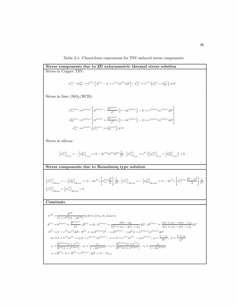
36
Table 3.1: Closed-form expressions for TSV-induced stress components
Stress components due to 2D axisymmetric thermal stress solutionStress in Copper TSV:
σCurr =σCu
θθ = CCuh
ACu − (1 + νCu)αCu∆Ti
; σCuzz = νCu
“
σCurr + σCu
θθ
”
6= 0
Stress in liner (SiO2/BCB):
σLinerrr =CLiner
"
ALiner −BLiner
r2
“
1 − 2νLiner”
− (1 + νLiner)αLiner∆T
#
σLinerθθ =CLiner
"
ALiner +BLiner
r2
“
1 − 2νLiner”
− (1 + νLiner)αLiner∆T
#
σCuzz =νLiner
“
σLinerrr + σLiner
θθ
”
6= 0
Stress in silicon:
h
σSirr
i
axi= −
h
σSiθθ
i
axi= (1 − 2νSi)CSiBSi 1
r2;
h
σSizz
i
axi= νSi
“h
σSirr
i
axi+
h
σSiθθ
i
axi
”
= 0
Stress components due to Boussinesq type solution
h
σSirr
i
Bou1= −
h
σSiθθ
i
Bou1= (1 − 2ν
Si)
"
σCuzz
a2
2
#
1
r2;
h
σSirr
i
Bou2= −
h
σSiθθ
i
Bou2= (1 − 2ν
Si)
"
σLinerzz
b2 − a2
2
#
1
r2
h
σSizz
i
Bou1=
h
σSizz
i
Bou2= 0
Constants
CM =EM
(1 + νM )(1 − 2νM )forM ∈ Cu, Si, Liner
ACu =ALiner +BLiner
a2;BCu = 0; ALiner =
mh− ng
h(1 + c2) − g(1 − c4)∆T ; BLiner =
n(1 + c2) −m(1 − c4)
h(1 + c2) − g(1 − c4)∆T
ASi =(1 + νSi)αSi∆T ; BSi = c2ALinerb2 − c1B
Liner − c2b2(1 + νLiner)αLiner∆T
m =(1 + νSi)αSi + c2(1 + νLiner)αLiner; n = (1 + νCu)αCu − c4αLiner; g =
1 − c1
b2; h =
1 + c3
a2
c1 =ELiner(1 + νSi)
ESi(1 + νLiner); c2 =
c1
1 − 2νLiner; c3 =
ELiner(1 + νCu)
ECu(1 + νLiner); c4 =
c3
1 − 2νLiner
a =RCu; b = RCu + tLiner; ∆T = T − Tref

37 Unlike cylindrical coordinates, there is a nonzero shearing (τxy) stress component in Carte-
sian coordinates. This value for the uniaxial case is half the magnitude of that in the biaxial
case. The magnitudes and signs of stress components in the biaxial and uniaxial formulations
differ, and the corresponding relative errors in mobility variation are quantified in Sec-
tion 3.4.1. As in cylindrical coordinates, the stress components are linear functions of the temperature
T due to their dependence on the factor C.
3.3.2 Impact of the crystal orientation
As mentioned in Chapter 2, the stresses need to be transformed along the transistor channel
directions, which correspond to wafer flat direction. It may be recalled that the wafer flat
direction corresponds to [110] Miller index direction and the chip surface has (001) orientation.
Thus, the stress distributions need to be evaluated along the [110] Miller index direction. By
examination of Figure 2.2(b), a rotation by 45 causes the axial direction to move along the
transverse direction. We can thus easily deduce the biaxial stress tensors in these coordinates
from equations (3.5) to be:
σx′x′ = −σy′y′ = τxy; τx′y′ = −σxx (3.7)
(a) (b)
Figure 3.4: Stress contour fields in the [110]-[110] axes. (a) σx′x′ stress contour field. (b) τx′y′
stress contour field.
The Fig. 3.4 shows the stress contours of σx′x′ and τx′y′ . The stress patterns are seen to
be tensile and compressive in mutually perpendicular directions. This results from the cos 2θ
[sin 2θ] term in σxx [τxy] in equation (3.5).

38
In contrast, for the uniaxial case used in several previous papers, since σθθ is set to 0, the
stress components are unchanged under rotation, i.e.,
σx′x′ = σxx; σy′y′ = σyy; τx′y′ = τxy. (3.8)
3.3.3 Comparison with finite element simulation
To validate the effectiveness of the closed-form 2D analytical solution in equation (3.4), we
perform 3D FEA simulations using the ABAQUS [30] tool with realistic TSV structures. As
stated earlier, since we are interested in modeling the degradation of the devices, our region
of interest lies outside the KOZ. In our experiments, we define the KOZ to be 1µm from the
edge of the TSV or 3.5µm from the center of the TSV, and is chosen to ensure that there is
no more than 33% mobility variation in any transistor around an isolated TSV. In practice, the
KOZ constraint is driven by the mobility degradation of PMOS transistors, which exceeds that
of NMOS devices. The effect of the copper landing pad is ignored in this analysis, since the
landing pad size is always within the KOZ boundary and its main influence is felt only at the
edge of the TSV.
All materials (TSV, liner, silicon) are assumed to be linear, elastic, and isotropic. The
annealing process is modeled in FEA by applying a temperature load with an initial temperature
of 250C and final temperature of 25C. For the 3D FEA simulations, the copper TSV diameter
is 5µm, height is 30µm, and the liner thickness is 125nm [52]. The mechanical properties of the
materials are listed in Table A.1.
(a) (b)
Figure 3.5: Comparison of (a) σrr and (b) σθθ between the analytical and the FEA models.Here TSV edge = 2.5µm, liner edge = 2.625µm, and KOZ edge = 3.5µm.
The analytical solution is compared against actual FEA stress with BCB and SiO2 liners,
respectively. Fig. 3.5 shows the comparison of the corresponding models against σrr and σθθ
components. It can be observed that the analytical models closely follow their FEA counterparts
outside the KOZ. The small errors between the analytical solution and FEA can be attributed

39
to the assumption of a homogeneous TSV structure (silicon) in the Boussinesq subproblems.
It will be shown in Section 3.6 that the worst case error in actual gate delay computations,
using the analytical models as compared to the FEA models, is less than 1ps for a two input
NAND gate in the library.
3.4 Effects of stress on electrical parameters
The stress distributions obtained in the previous section can be used to evaluate changes in
transistor mobility and threshold voltage using piezoresistivity and deformation potential theory
models, respectively, introduced in Section 2.3.
3.4.1 TSV-induced mobility variations.
Using the piezoresistivity model presented in Section 2.3.1 in the rotated (x′, y′) coordinate
system, the relative change in mobility under TSV-induced stress is given by the expression:
∆µ′
µ′= [π′
11σx′x′ + π′12σy′y′ ] cos2 φ′
+ [π′11σy′y′ + π′
12σx′x′ ] sin2 φ′ + [π′44τx′y′ ] sin 2φ′ (3.9)
Here, π′11, π′
12 and π′44 are the three unique piezoresistivity coefficients defined along the primed
coordinate axes, and φ′ is the angle made by the transistor channel with the x′-axis, i.e., the
[110] axis. This implies that φ′ = 0 for the transistor channels that are oriented along this
direction, and φ′ = π/2 when they are orthogonal to this axis. As we have seen earlier, the
piezoresistivity coefficients and the stress tensor components vary with the channel orientation,
implying that the mobility variation depends on the transistor channel orientation. Biaxial
case: For a transistor oriented along the [110] axis, φ′ = 0. From equations (3.7), (3.9), and
(2.7),
∆µ′
µ′= π′
11σx′x′ + π′12σy′y′ = π44σx′x′ = π44σrr sin 2θ. (3.10)
Recall that θ is the angle made by the vector from the origin to the center of the transistor with
the unprimed x-axis. Similarly, for a transistor in the orthogonal direction, φ′ = π/2, and
∆µ′
µ′= π′
11σy′y′ + π′12σx′x′
= −π44σx′x′ = −π44σrr sin 2θ. (3.11)
Based on the above analysis, we can observe that:

40 For the same stress and orientation, PMOS and NMOS devices experience opposite mobil-
ity variation effects: both depend on π44, which has a different sign for PMOS and NMOS
(Table A.2). For the same stress, PMOS devices experience greater mobility variation as compared to
NMOS devices, since the π44 value of PMOS is an order of magnitude greater than that
of the NMOS as seen in [53]. The relative mobility variation depends on the operating temperature since stress varies
linearly with temperature as pointed out in Section 3.2.
Uniaxial case: For φ′ = 0, from equations (3.6), (3.8), and (3.9), the corresponding mobility
variation can be expressed as:
∆µ′
µ′= π′
11σx′x′ + π′12σy′y′ = π′
11σrr cos2 θ + π′12σrr sin2 θ. (3.12)
For the orthogonal transistor orientation, φ′ = π/2, and therefore
∆µ′
µ′= π′
11σy′y′ + π′12σx′x′ = π′
11σrr sin2 θ + π′12σrr cos2 θ. (3.13)
0 2 4 6 8 10 12 14 16 18 20−30−25−20−15−10−5
05
1015
Distance along y′ axis (µm)
Mob
ility
Var
iatio
n (%
)
PMOS biaxialPMOS uniaxialNMOS biaxialNMOS uniaxial
KOZ edge
Liner edge
TSV
(a)
0 2 4 6 8 10 12 14 16 18 20−10−5
05
10152025303540
Distance along x′ axis (µm)
Mob
ility
Var
iatio
n (%
)
PMOS biaxialPMOS uniaxialNMOS biaxialNMOS uniaxial
KOZ edge
Liner edge
TSV
(b)
Figure 3.6: Mobility variation comparison in uniaxial and biaxial formulations with distancealong (a) y′-axis (b) x-axis. Here TSV edge = 2.5µm, liner edge = 2.625µm, and KOZ edge =3.5µm.
Comparison: From equation (3.5), TSV stress is biaxial, and we now examine the error from
the uniaxial assumption. We consider transistors oriented along the [110] axis (φ′ = 0). From
equations (3.10) and (3.12) , the relative mobility variation depends only upon π44 in the biaxial
formulation, while in the uniaxial formulation it depends on π′11 and π′
12. Fig.3.6 shows the
mobility variations in NMOS/PMOS transistors at room temperature (25C) with biaxial and
uniaxial stress formulations. The inaccuracies in using the uniaxial formulation can be identified
by observing two cases:

41 θ = π2 (Fig. 3.6 (a)): For the NMOS transistor, the biaxial analysis correctly predicts a
mobility degradation while the uniaxial case mispredicts an improvement. For the PMOS
transistor, both formulations predict a mobility improvement, but the uniaxial formulation
underestimates the variation. φ′ = 0 (Fig. 3.6 (b)): For the same stress, the uniaxial case shows the same trends with
T as the biaxial case, but overestimates the NMOS mobility variation and underestimates
PMOS variation. The percentage inaccuracies are significant.
3.4.2 TSV-induced threshold voltage variations
As seen from Section 2.3 of Chapter 2, applied mechanical stress causes shifts and splits in
conduction and valence band potentials. The changes in conduction and valence band potentials
are expressed as a function of strain components as seen from Equation 2.9. Here, the strain
components correspond to the TSV-induced strains in Cartesian coordinate system. The strains
can be obtained from the stresses in equation (3.5) as
ǫxx =1
ESi
(
σxx − νSi (σyy + σzz))
ǫyy =1
ESi
(
σyy − νSi (σzz + σxx))
ǫxy =1 + νSi
ESiτxy
ǫzz = ǫyz = ǫzx = 0 (3.14)
From equations (3.5) and (3.14), it can be deduced that ǫxx = −ǫyy, and ǫzz = 0. Thus, the
hydrostatic contribution in Equation (2.9), ǫxx+ǫyy+ǫzz = 0. Hence, under TSV-induced stress,
there is only splitting of conduction and valence bands without any hydrostatic shifts. This is
unlike the process induced strains in [2] where both hydrostatic shifts and shear splits take place
in electronic bands. The net effect is a smaller variation in electronic band gap potential due
to TSV-induced stress. Regardless of the strain type, the energy band gap has been shown to
decrease [54,37]. Thus threshold voltage is also expected to decrease under TSV-induced stress.
The threshold voltage is a function of band-gap potential and thus can be expressed as a
function of the changes in conduction band and valence band potentials. Ignoring the changes
in the densities of states whose contributions are negligible [41], we have:
q∆V TSVtp = m∆EC − (m − 1)∆EV
q∆V TSVtn = m∆EV − (m − 1)∆EC (3.15)
where ∆V TSVtp and ∆V TSV
tn are the changes in PMOS and NMOS threshold voltages, respec-
tively, due to TSV-induced effects. It may be recalled from Section 2.3.3 that ∆EC represents

42
the minimum of the changes in conduction band potentials, ∆EiC . Since conduction band is low-
ered under TSV-induced stress, ∆EC is negative valued. The term ∆EV denotes the maximum
of the changes in valence band potentials, ∆EhhV and ∆Elh
V , and is positive valued. This leads to
decrease in bandgap potential consistent with [54, 37]. The work in [55] uses similar models to
predict TSV-induced threshold voltage variation of upto 8mV, but uses the generalized process
strain equations in [2] which is not valid for TSV-induced strains. Furthermore, in the same
work, there is a sign error in the usage of ∆EC and band gap potential. This leads to errors
in threshold voltage computations, although the actual changes in threshold voltage are still
within 15mV under TSV effects.
(a) (b)
Figure 3.7: TSV-induced threshold voltage variation in (a) PMOS transistor (b) NMOS tran-sistor. Here TSV edge = 2.5µm, liner edge = 2.625µm, and KOZ edge = 3.5µm.
Based on the above analysis, the threshold voltage variations of PMOS and NMOS tran-
sistors are plotted in Fig. 3.7 at the room temperature (25oC). We can observe that threshold
voltage for the PMOS and NMOS have decreased; positive [negative] shifts for PMOS [NMOS].
Furthermore, beyond a short distance from the KOZ edge, the threshold voltage variations are
practically zero. The patterns can be explained by the relations in equations 2.9 and 3.15. The
threshold voltage improvements suggest leakage power degradations.
3.5 Timing analysis under electrical variations
Our circuit-level input is a characterized cell library and a placed netlist, based on which the
stresses may be computed using the techniques in Section 3.2; this stress can be converted
to determine the transistor mobility and threshold voltage variations, using the methods in
Section 3.4.

43
3.5.1 Delay dependence on temperature
We first consider the effects of temperature on delay without TSV stress and then add the TSV
stress effects.
The traditional assumption that has guided timing analysis is that the delays of library
cells increase monotonically with temperature, corresponding to the NTD case. However, with
technology scaling and the increased use of lower Vdd and Vt values, PTD and MTD are also
often seen. Gate delays change with T in two ways:
(1) The mobility change for charge carriers, ∆µT , is given by:
∆µT = µ (T0) (T/T0)−m (3.16)
Here T0 is the room temperature, and m > 0 is the mobility temperature exponent, with a
typical value of 1.7 in highly doped silicon, and 1.4 in nanometer silicon layers, where boundary
scattering becomes important [56]. This reduction in µ increases the delay.
(2) The threshold voltage change, ∆Vt, for a transistor is given by:
∆Vt = −κ (T − T0) (3.17)
where κ > 0 has a typical value of 2.5mV/K [57]. Thus, the delay decreases with T due to this
effect.
The two phenomena above have opposite effects on gate delays, and depending on which of
the two is more dominant, results in PTD, NTD, or MTD effects.
3.5.2 Gate characterization
The variation in the low-field mobility and threshold voltage translates into variations in the
gate delay metric. Since changes in saturation velocity are correlated to the changes in low-field
mobility as seen from equation (2.8), it suffices to express changes in gate delays in terms of
changes in low-field mobility and threshold voltage. The delay, Dstr, of a gate under stress is
given by:
Dstr = Dnom +
(
∂D
∂µ
)
(∆µTSV + ∆µT ) +
(
∂D
∂Vt
)
(
∆V TSVt + ∆Vt
)
(3.18)
where Dnom is the delay without temperature or TSV effects, ∂D/∂µ [∂D/∂Vt] is the sen-
sitivity of the delay to mobility [Vt] variation at the nominal point, and ∆µTSV [∆V TSVt ] is
the mobility [threshold voltage] change due to TSV stress. Note that the sensitivity ∂D/∂µ
accounts for both low-field mobility and saturation velocity. For the 45nm technology used in
our work, the changes in velocity saturation account for less than 1% change in gate delays.
In this work, the delay variations are primarily due to the changes low-field mobility and the
threshold voltage.

44
The mobility sensitivity is a nonlinear function of the nominal point, and is stored as a look-up
table (LUT) rather than a constant sensitivity value. On the other hand, the threshold voltage
sensitivity is a linear function of the nominal point. During delay calculation, linear interpolation
is used between the stored points. This results in improved accuracy, e.g., for a NAND2 gate
in the library, the delay error using our approach is less than 3%. LUT characterization is a
one-time exercise for a library. The range of the LUT reflects the observed range of variations.
For example, for mobility sensitivity, using HSPICE, we characterize a 45nm gate library for five
delay values with corresponding PMOS mobility variations ranging from ±50%. For the NMOS
mobility variations, we use a linear approximation considering a range of ±5%. For threshold
voltage sensitivity, we characterize the gate library at the nominal threshold voltage and with a
shift of -20 mV [20 mV] in NMOS [PMOS] transistors. The library characterization is performed
from −25C to 125C, along with different supply voltages, load capacitances, and input slopes.
The leakage power of a transistor exponentially increases (decreases) with its decreasing (in-
creasing) threshold voltage. However, for small changes in threshold voltage of a transistor, the
gate-level leakage power varies almost linearly. As seen in Fig. 3.7, the TSV-induced threshold
voltage variations in transistors are typically few tens of millivolts not exceeding 15 mV. For the
TSV-induced stress, all the transistors of the same type (NMOS or PMOS) experience equal
magnitude of threshold voltage shifts. This is because TSV-stress spans an area that is consid-
erably larger than the individual layouts of the logic gates. Thus, if there are n transistors in a
gate, the total leakage power of the gate is given by:
Lstrgate = Lnomgate +n
∑
i=1
∂Lgate∂Vti
∣
∣
∣
∣
0
∆V TSVti (3.19)
where Lstrgate is the leakage power of a gate under TSV-induced stress and Lnomgate is the nominal
leakage power of the gate under no stress. The partial derivative of Lgate with Vti represents the
sensitivity of the leakage current of the gate to changes in the threshold voltage of transistor i,
evaluated at the nominal point. ∆V TSVti denotes the threshold voltage shift in the transistor i.
Note that all the NMOS or PMOS transistors in a gate correspondingly have the same ∆Vti. In
our work, the relative error in estimating the gate leakage power of the standard cells with this
approach is under 1%.
3.5.3 Timing analysis framework
For the placed netlist that is provided as an input to the procedure, the left bottom coordinates
and width and height of each cell in the layout can be determined. The computation then
proceeds as follows: First, from the above placement information, the centers of the TSV and
the standard cells are computed. Second, the equations in (3.7) and (3.14) are used to calculate
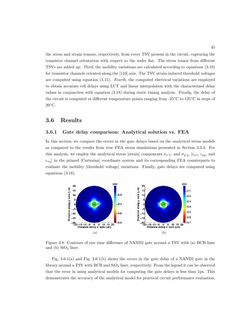
45
the stress and strain tensors, respectively, from every TSV present in the circuit, capturing the
transistor channel orientation with respect to the wafer flat. The stress tensor from different
TSVs are added up. Third, the mobility variations are calculated according to equations (3.10)
for transistor channels oriented along the [110] axis. The TSV strain-induced threshold voltages
are computed using equation (3.15). Fourth, the computed electrical variations are employed
to obtain accurate cell delays using LUT and linear interpolation with the characterized delay
values in conjunction with equation (3.18) during static timing analysis. Finally, the delay of
the circuit is computed at different temperature points ranging from -25C to 125C in steps of
20C.
3.6 Results
3.6.1 Gate delay comparison: Analytical solution vs. FEA
In this section, we compare the errors in the gate delays based on the analytical stress models
as compared to the results from true FEA stress simulations presented in Section 3.3.3. For
this analysis, we employ the analytical stress [strain] components σx′x′ and σy′y′ [ǫxx, ǫyy, and
ǫxy] in the primed [Cartesian] coordinate system and its corresponding FEA counterparts to
evaluate the mobility [threshold voltage] variations. Finally, gate delays are computed using
equations (3.18).
(a) (b)
Figure 3.8: Contours of rise time difference of NAND2 gate around a TSV with (a) BCB linerand (b) SiO2 liner.
Fig. 3.6.1(a) and Fig. 3.6.1(b) shows the errors in the gate delay of a NAND2 gate in the
library around a TSV with BCB and SiO2 liner, respectively. From the legend it can be observed
that the error in using analytical models for computing the gate delays is less than 1ps. This
demonstrates the accuracy of the analytical model for practical circuit performance evaluation,

46
and thus removes the need for storage overhead of store FEA models, or the computational
overhead of on-the-fly FEA.
3.6.2 Effect of TSV-induced stress on circuit path delays.
We apply our techniques on a set of IWLS 2005 benchmarks [58] whose attributes are as shown
in Table 3.2, where #PO denotes the number of primary outputs in the design. The parameters
chosen in our experiments are listed below: The analytical stress and strain models for TSV with BCB and SiO2 liners, respectively. A cell library characterized under the 45nm PTM [59]. All transistor orientations parallel to the [110] axis. A TSV diameter of 5µm. The TSV is surrounded by either BCB or SiO2 liner with a liner
thickness of 125nm. Our KOZ is defined as the point where the mobility variations are below 33%; this corre-
sponds to a KOZ size of 1µm from the TSV edge. For scaled technologies, a TSV diameter of 3µm [1µm] with SiO2 liner and a KOZ size of
0.6µm [0.2µm].
Figure 3.9: FO4 rise delay variation of a NAND2 gate with different TSV diameters. TheNAND2 gate is at a distance d from the KOZ edge.
The Fig. 3.9 shows the FO4 rise delay variation of a NAND2 gate in the library at 25C
with TSV diameters of 5µm, 3µm, and 1µm. In all the cases, the NAND2 gate is at a fixed
distance of 100nm/500nm/1µm from the KOZ edge of the corresponding TSVs. Furthermore,
the centers of the standard cell and the respective TSVs are aligned along x′-axis. From the
figure, it can be seen that for a fixed distance from the TSV the delay variation decreases as
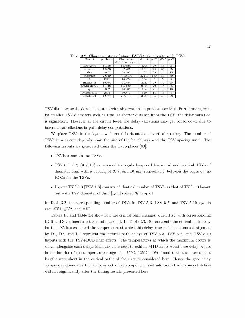
47
Table 3.2: Characteristics of 45nm IWLS 2005 circuits with TSVsCircuit # Gates Dimension # POs #V1 #V2 #V3
H×W (µm×µm)ac97 ctrl 11308 130×80 4204 70 54 35aes core 12223 87×85 12313 49 36 25
des 4647 68×85 332 35 24 15ethernet 29739 104×170 32149 170 84 60
i2c 1221 16×74 204 6 5 4mem ctrl 10094 94×84 2522 49 36 25
pci bridge32 11148 127×85 9025 70 48 35spi 3632 48×87 564 21 18 10
systemcdes 2694 50×71 549 18 15 8usb funct 12987 76×113 3930 54 40 28
TSV diameter scales down, consistent with observations in previous sections. Furthermore, even
for smaller TSV diameters such as 1µm, at shorter distance from the TSV, the delay variation
is significant. However at the circuit level, the delay variations may get toned down due to
inherent cancellations in path delay computations.
We place TSVs in the layout with equal horizontal and vertical spacing. The number of
TSVs in a circuit depends upon the size of the benchmark and the TSV spacing used. The
following layouts are generated using the Capo placer [60]: TSVless contains no TSVs. TSV 5 i, i ∈ 3, 7, 10 correspond to regularly-spaced horizontal and vertical TSVs of
diameter 5µm with a spacing of 3, 7, and 10 µm, respectively, between the edges of the
KOZs for the TSVs. Layout TSV 3 3 [TSV 1 3] consists of identical number of TSV’s as that of TSV 5 3 layout
but with TSV diameter of 3µm [1µm] spaced 3µm apart.
In Table 3.2, the corresponding number of TSVs in TSV 5 3, TSV 5 7, and TSV 5 10 layouts
are: #V1, #V2, and #V3.
Tables 3.3 and Table 3.4 show how the critical path changes, when TSV with corresponding
BCB and SiO2 liners are taken into account. In Table 3.3, D0 represents the critical path delay
for the TSVless case, and the temperature at which this delay is seen. The columns designated
by D1, D2, and D3 represent the critical path delays of TSV 5 3, TSV 5 7, and TSV 5 10
layouts with the TSV+BCB liner effects. The temperatures at which the maximum occurs is
shown alongside each delay. Each circuit is seen to exhibit MTD as its worst case delay occurs
in the interior of the temperature range of [−25C, 125C]. We found that, the interconnect
lengths were short in the critical paths of the circuits considered here. Hence the gate delay
component dominates the interconnect delay component, and addition of interconnect delays
will not significantly alter the timing results presented here.

48
Table 3.3: Comparison of critical path delay of circuits without and with TSV + BCB linereffects
Circuit TSVless TSV 5 3 TSV 5 7 TSV 5 10D0 T D1 T ∆D1 D2 T ∆D2 D3 T ∆D3(ps) (C) (ps) (C) (%) (ps) (C) (%) (ps) (C) (%)
ac97 ctrl 505 55 501 35 -0.8% 500 35 -1.0% 504 35 -0.2%aes core 516 35 519 35 0.6% 538 15 4.3% 511 15 -1.0%
des 1024 35 1023 15 -0.1% 1024 15 0.0% 1022 35 -0.2%ethernet 914 15 919 -5 0.5% 902 15 -1.3% 903 15 -1.2%
i2c 444 35 443 15 -0.2% 445 35 0.2% 445 15 0.2%mem ctrl 979 35 983 15 0.4% 988 15 0.9% 983 15 0.4%
pci bridge32 738 35 737 35 -0.1% 739 35 0.1% 733 15 -0.7%spi 954 15 957 15 0.3% 960 15 0.6% 951 15 -0.3%
systemcdes 855 15 859 -5 0.5% 865 -5 1.2% 855 15 0.0%usb funct 702 15 712 15 1.4% 704 15 0.3% 697 15 -0.7%
TSVs act as blockages for cell placement. When the TSV pitch changes, the locations of
these blockages change, and therefore the circuit placement changes. Since the four layouts in
Table 3.3 are different, these delays should not be directly compared. However, the portion of
the delays, ∆Di, i ∈ 1, 2, 3, can explicitly be attributed to the TSV+liner effects (clearly, ∆D0
is zero in the TSVless layout). To compute each ∆Di, we first find the critical path delay for the
corresponding layout while ignoring TSV stress effects, then the critical path delay when TSV
stresses are added in, and we show the percentage change. The liner effects are always considered
when the TSV is present. In Table 3.4, the columns ∆D4, ∆D5, and ∆D6 represent the changes
in delay of circuits TSV 5 3, TSV 5 7, and TSV 5 10, respectively, with TSV+SiO2 liner. The
corresponding changes in circuits TSV 3 3 and TSV 1 3 are shown in columns denoted by ∆D7
and ∆D8. Note that the critical path can (and often does) change with TSV stress.
Table 3.4: Critical path delay of circuits with TSV + SiO2 liner effectsCircuit TSV 5 3 TSV 5 7 TSV 5 10 TSV 3 3 TSV 1 3
T ∆D4 T ∆D5 T ∆D6 T ∆D7 T ∆D8(C) (%) (C) (%) (C) (%) (C) (%) (C) (%)
ac97 ctrl 35 -0.8% 35 -1.4% 35 0.2% 35 0.2% 15 -0.2%aes core 35 1.0% 15 6.4% 35 -1.4% 15 1.4% 35 0.0%
des 15 0.9% 35 0.6% 35 -0.3% 15 0.6% 35 0.1%ethernet 15 1.4% -5 -1.2% 15 -1.4% 15 -0.8% 15 -0.1%
i2c -125 0.5% 15 0.5% 15 0.5% 15 -0.2% 35 -0.2%mem ctrl 35 0.8% 15 1.3% 15 0.5% 15 0.6% 15 0.4%
pci bridge32 35 -0.1% 35 0.1% 35 -0.8% 35 -0.4% 35 0.0%spi 15 0.5% 15 1.2% 15 -0.4% 15 1.5% 15 0.1%
systemcdes -5 3.0% -5 1.8% 15 -0.1% -5 1.3% 15 0.0%usb funct -125 3.1% 15 1.6% 15 -0.9% 15 -0.4% 15 -0.1%
The improvements (negative changes) in critical path delays indicate that even with the
smaller, more aggressive KOZ used here, we can mitigate the TSV effects on the critical path
delays to some extent by careful design choices during initial circuit placement. Additionally,
temperature dependence of the circuits is also altered when TSV effects are taken into account.
In Table 3.4, although circuits TSV 5 3, TSV 3 3, and TSV 1 3 contain identical number of

49
TSVs, the differences in the changes in critical path delay of individual circuits can be attributed
to the difference in relative placement of the gates with respect to the TSVs. The TSV 5 3 circuit
shows a delay variation of -0.8 to 3.1% while TSV 3 3 [TSV 1 3] circuit shows a variation of -0.8
to 1.5% [-0.2 to 0.4%]. Thus, it can be concluded that even with smaller dimensions of TSVs,
the stress effects on circuit timing cannot be ignored.
From Tables 3.3 and 3.4, it can be observed that there is a wider range of delay variation in
the TSV inserted layouts with SiO2 liner as compared to the corresponding layouts with BCB
liner. For instance, in the TSV 5 7 layouts, the critical path variations with SiO2 liner ranges
from -1.4% to 6.4%. The corresponding variation within the same layout with the BCB liner
taken into account ranges from -1.3 to 4.3%. Similar trends can be observed in the TSV 5 3 and
TSV 5 10 layouts. The smaller magnitude of variations in using a BCB liner indicates that the
BCB liner is preferable over SiO2 liner from a circuit timing perspective. The improvement in
mechanical reliability in using BCB liner over SiO2 is already shown in [46]. For these reasons,
we shall focus on the layouts with TSV+BCB liner for the rest of the discussion.
Table 3.5: Delay changes in the TSV 5 7 circuits with TSV + BCB linerCircuit DP1 ∆DP1 DP2 ∆DP2 DP3 ∆DP3 ∆TPS ∆TNS
(ps) (%) (ps) (%) (ps) (%) (ps) (ps)ac97 ctrl 505 -1.0% 361 5.8% 347 -5.5% -1135 0aes core 513 4.9% 536 4.3% 423 -4.7% 13543 -269
des 1012 1.2% 783 4.0% 833 -3.1% 261 -10ethernet 908 -0.7% 624 4.5% 596 -5.4% 23566 0
i2c 443 0.5% 344 4.4% 295 -5.1% 29 -2mem ctrl 979 0.9% 597 4.9% 573 -4.5% -327 -85
pci bridge32 715 3.4% 566 4.8% 645 -4.2% -217 -1spi 951 0.9% 800 3.5% 675 -4.0% -53 -26
systemcdes 837 3.3% 742 3.6% 485 -5.4% 1313 -13usb funct 684 2.9% 619 3.9% 360 -5.8% 4850 -22
In order to gain more insights into the circuit timing behavior we further examine the
TSV 5 7 circuits in detail. Let P1 denote the critical path in the circuit with TSV effects.
Let P2 and P3 represent the paths that show maximum delay degradation, and delay improve-
ment, respectively, when TSV effects are considered. For each circuit, Table 3.5 describes the
extent of delay changes in these paths due TSV-induced mobility variations. Here DP1, DP2
and DP3 denote the nominal path delays of paths P1, P2, and P3, respectively, and ∆DP1,
∆DP2, and ∆DP3, respectively, are the changes in the delay of each of these paths due to TSV-
stress-induced variations. Note that DP1 and ∆DP1 together evaluate to the actual critical
path delay of the circuit show in column D2 of Table 3.3. This table also shows the amount of
change in the circuit total positive slack (TPS) and the total negative slack (TNS) when TSV
effects are considered, are denoted by ∆TPS and ∆TNS, respectively. While computing slacks,
we consider the worst case path delay of the circuit without TSV effects as the required time
specification to be met. From the table we can observe that:

50 The actual change on the critical path denoted by ∆DP1 can be more than the change in
the worst case path delay observed at the circuit level shown in ∆D2 in Table 3.3. A noncritical path can become timing-critical when TSV effects are considered. This is
observed by comparing the delays in DP1 and its percentage change, ∆DP1 in Table 3.5
with the circuit critical path delay D2 and the circuit level change, ∆D2 in Table 3.3. The maximum delay degradation or improvement, given by ∆DP2 and ∆DP3, respectively,
among all paths is significantly greater than the worst case path delay changes observed
at the circuit level. The negative [positive] changes in ∆TPS of the circuits reveal that a majority of paths ex-
perience delay degradation [improvement] and there is lower [more] positive slack available
in the circuit under TSV effects. The wide distribution in the ∆TNS indicates that many non-critical paths in the circuit
can violate timing constraints when TSV effects are taken into account.
(a) (b)
Figure 3.10: Delay changes for benchmark spi (a) PMOS ∆Delay map (b) NMOS ∆Delay map.
Fig. 3.10 shows the color maps of the delay changes in PMOS and NMOS transistors in the
gates for the spi circuit. The square white portions represent the TSV locations. Consistent
with Figure 3.4, we see that maximum delay changes are observed in the horizontal and vertical
regions between the TSVs. Furthermore, it can be observed that minimum delay variations occur
in the regions diagonal to the TSVs. From the scales, it can be noticed that PMOS transistors
tend to experience greater magnitude of delay variations than NMOS transistors. The effect
of threshold voltage improvements seen in Fig. 3.7 suggests that for regions closer to the KOZ,
mobility degradations are attenuated to an extent while mobility improvements are fortified.
Since threshold voltage changes vanish after a short distance beyond KOZ, mobility variations
are predominant at further distance from the KOZ. From the Fig. 3.10, it can be concluded that
path delay degradations [improvements] are due to the gates placed in the horizontal [vertical]
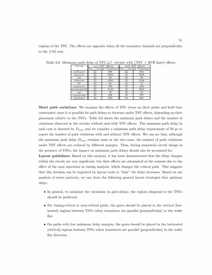
51
regions of the TSV. The effects are opposite when all the transistor channels are perpendicular
to the [110] axis.
Table 3.6: Minimum path delay of TSV 5 7 circuits with TSV + BCB liner effectsCircuit w/o TSV effects with TSV effects
Dmin(ps) # Violations Dmin(ps) # Violationsac97 ctrl 22 998 22 984aes core 22 3802 22 3485
des 29 28 29 28ethernet 22 2480 22 2448
i2c 22 80 22 73mem ctrl 22 500 22 449
pci bridge32 22 4140 22 4045spi 22 48 22 43
systemcdes 29 238 29 237usb funct 22 908 22 881
Short path variations: We examine the effects of TSV stress on short paths and hold time
constraints, since it is possible for path delays to decrease under TSV effects, depending on their
placement relative to the TSVs. Table 3.6 shows the minimum path delays and the number of
violations observed in the circuits without and with TSV effects. The minimum path delay in
each case is denoted by Dmin and we consider a minimum path delay requirement of 50 ps to
report the number of path violations with and without TSV effects. We can see that, although
the minimum path delay Dmin remains same in the two cases, the number of path violations
under TSV effects are reduced by different margins. Thus, during sequential circuit design in
the presence of TSVs, the impact on minimum path delays should also be accounted for.
Layout guidelines: Based on this analysis, it has been demonstrated that the delay changes
within the circuit are very significant, but their effects are attenuated at the outputs due to the
effect of the max operation in timing analysis, which changes the critical path. This suggests
that this freedom can be exploited by layout tools to “hide” the delay increases. Based on our
analysis of stress patterns, we can draw the following general layout strategies that optimize
delay: In general, to minimize the variations in gate-delays, the regions diagonal to the TSVs
should be preferred. For timing-critical or near-critical paths, the gates should be placed in the vertical [hor-
izontal] regions between TSVs when transistors are parallel [perpendicular] to the wafer
flat. On paths with low minimum delay margins, the gates should be placed in the horizontal
[vertical] regions between TSVs when transistors are parallel [perpendicular] to the wafer
flat direction.

52
3.6.3 TSV-induced stress effects on leakage power
TSV-induced stress causes threshold voltage reductions in NMOS/PMOS transistors as seen in
Section 3.4.2. Thus, the leakage power of the circuits are expected to degrade under TSV effects.
To evaluate TSV effects on leakage power, we compare the leakage power of the TSV 7 layouts
at room temperature (25C), under TSV with SiO2/BCB liner effects, with the TSVless layouts
where the TSV-stress effects are not present. In Table 3.7, L0 denotes the leakage power in the
TSVless layouts. Furthermore, the columns L1 and L2 [∆L1 and ∆L2] represent the actual
leakage power [changes in the leakage power] under TSV effects with SiO2 and BCB liners,
respectively. Obviously, here ∆L0 is zero.
In Table 3.7, the positive changes in ∆L1 and ∆L2 indicate that leakage power is higher or
degrades under TSV-induced stress effects. This shows that if TSV-induced threshold voltage is
not taken into account, leakage power of the circuit is underestimated. The increase in leakage
power when SiO2 [BCB] liner is taken into account varies from 3.7% to 5.7% [2.5% to 3.8%].
Thus for the same TSV geometry and KOZ, a TSV with SiO2 liner causes greater leakage
degradations as compared to the BCB liner case. Since the TSV-induced stress with SiO2 liner
has a greater magnitude than the BCB liner case, the former liner case causes wider range of
circuit timing and leakage power variations than the latter case.
Table 3.7: Leakage power of TSV 5 7 circuitsCircuit w/o TSV TSV + SiO2 liner TSV + BCB liner
L0 (mW) L1 (mW) ∆L1 (%) L2 (mW) ∆L2 (%)ac97 ctrl 14.04 14.75 5.1% 14.52 3.4%aes core 14.72 15.32 4.1% 15.13 2.8%
des 6.3 6.61 4.9% 6.51 3.3%ethernet 31.8 32.97 3.7% 32.59 2.5%
i2c 1.58 1.67 5.7% 1.64 3.8%mem ctrl 12.44 12.95 4.1% 12.79 2.8%
pci bridge32 15.82 16.503 4.3% 16.28 2.9%spi 4.44 4.63 4.3% 4.57 2.9%
systemcdes 3.96 4.15 4.8% 4.09 3.3%usb funct 14.73 15.29 3.8% 15.11 2.6%
3.7 Conclusion
Through silicon vias cause layout-dependent electrical variations in 3D-IC circuits. A holistic
framework is presented that considers TSV-stress and other thermal effects on transistor elec-
trical parameters. The analytical stress model presented in this chapter is shown to accurately
capture the biaxial nature of the TSV-stress, with good agreement with FEA models. The
stresses and strains thus obtained are employed to evaluate variations in gate and circuit-level
performance metrics. A thorough analysis of path delays is presented and the effects of TSV-
stress on circuit leakage power is evaluated. Finally layout guidelines are suggested for improving
53
timing performance in 3D-ICs.
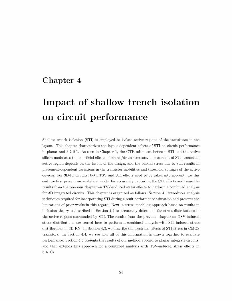
Chapter 4
Impact of shallow trench isolation
on circuit performance
Shallow trench isolation (STI) is employed to isolate active regions of the transistors in the
layout. This chapter characterizes the layout-dependent effects of STI on circuit performance
in planar and 3D-ICs. As seen in Chapter 1, the CTE mismatch between STI and the active
silicon modulates the beneficial effects of source/drain stressors. The amount of STI around an
active region depends on the layout of the design, and the biaxial stress due to STI results in
placement-dependent variations in the transistor mobilities and threshold voltages of the active
devices. For 3D-IC circuits, both TSV and STI effects need to be taken into account. To this
end, we first present an analytical model for accurately capturing the STI effects and reuse the
results from the previous chapter on TSV-induced stress effects to perform a combined analysis
for 3D integrated circuits. This chapter is organized as follows. Section 4.1 introduces analysis
techniques required for incorporating STI during circuit performance esimation and presents the
limitations of prior works in this regard. Next, a stress modeling approach based on results in
inclusion theory is described in Section 4.2 to accurately determine the stress distributions in
the active regions surrounded by STI. The results from the previous chapter on TSV-induced
stress distributions are reused here to perform a combined analysis with STI-induced stress
distributions in 3D-ICs. In Section 4.3, we describe the electrical effects of STI stress in CMOS
tranistors. In Section 4.4, we see how all of this information is drawn together to evaluate
performance. Section 4.5 presents the results of our method applied to planar integrate circuits,
and then extends this approach for a combined analysis with TSV-induced stress effects in
3D-ICs.
54
55
4.1 Introduction
In nanometer technologies, shallow trench isolation (STI) is used to isolate active transistor
regions in the layout. In typical fabrication technologies, shallow blocks of STI, made of SiO2, are
inserted into a much larger three-dimensional silicon structure. Figure 4.1 shows a representative
layout showing a 2D view of STI in and between standard cells.
During manufacturing, the STI oxide is grown from Si around an active region at a tem-
perature of 1000C using oxidation. When the chip returns to room temperature, the unequal
coefficients of thermal expansion (CTEs) of SiO2 and Si result in an unintentional residual ther-
mal stress in the active Si. The STI-induced stress tends to modulate the engineered stresses
in the transistor channels and can affect the mobility and threshold voltage of the transistors,
thus affecting the circuit performance. The work in [61] documents the impact of STI stress and
shows that the PMOS (NMOS) delay of a CMOS inverter improves (degrades) by about 17%
(8%) when moved from a denser layout region with many surrounding gates to a sparser region
with no neighbours.
Figure 4.1: A segment of a circuit layout showing how the STI in adjacent cells, or in gapsbetween cells, imply that the shape of an STI region depends on the layout of neighboring cells.
This STI-induced stress, and hence its performance impact, is highly layout-dependent since
STI surrounds and abuts the active region in the physical layout in nonuniform ways. Therefore,
the amount of STI around a transistor is determined by the relative locations and layouts of
its neighbouring cells. For instance, to evaluate the stress affecting gate g6 in the middle row
in Figure 4.1, we must consider STI contributions from its eight neighbours g2 through g10,
and also the STI within g6. Therefore, STI stress can only be correctly evaluated after layout.
In theory, it may be possible to precharacterize the stress by parameterizing the layout of
the neighbors of a cell, but the number of cases to be characterized for all possible neighbors
can be large. In the published literature [61, 62], the only known accurate method involves
computationally expensive finite element simulation for each transistor, which is impractical for
layouts of realistic-sized circuits.
56
An alternative to finite element simulations involves the use of analytical models, which
can be evaluated fast enough to permit the analysis of large layouts. Much of the literature
in this area [63, 64, 65, 66] is based entirely on the use of one-dimensional models that account
for stress components only along the longitudinal direction (i.e., along the channel direction).
However, finite element simulations in [61, 62] show that STI stress in the transverse direction,
perpendicular to the channel direction, also impacts the circuit performance. Furthermore,
[63,64,65,66] use only a single component of the stress tensor for performance evaluation, while
the entire stress tensor must be evaluated to accurately analyze STI-induced circuit performance
variation. The work in [67] uses both longitudinal and transverse direction STI contributions,
but is based on an empirically fitted model that is not scalable for nonrectangular shaped
active/STI regions.
In addition, STI is also present in 3D-IC circuits and both TSV and STI contribute to
the unintentional stresses in transistors which affect performance. Moreover, both the sets of
effects are layout-dependent. Analytical models developed for TSV-induced stress distributions
in the previous chapter can be used in conjunction with STI stress models in this chapter for a
combined analysis. The combined effects of STI and TSV in 3D-ICs were evaluated using both
FEM-based and analytical approaches. The work in [68] uses complex multi-scale finite element
simulations on the entire layout to predict stress distributions in silicon due to TSVs and STI.
The work in [69] employs analytical models to perform timing analysis in the presence of both
STI and the TSV. However, the work uses a simplistic uniaxial model for TSV and STI which
may not be accurate. Moreover, the library characterization in [69] assumes all the transistors
may experience similar mobility variations with STI+TSV effects. Although this may be true
for TSVs owing to their relative large size in the layout, the transistors within a standard cell
may experience differing magnitudes of electrical variations due STI in the immediate vicinity
of channel regions.
In this chapter, we present an analytical method to accurately capture the effects of STI on
circuit performance for a given layout, taking into account the three-dimensional geometry of
the STI together with its nonrectangular shape around an active region. Specifically, we model the effects of STI in the presence of intentional source/drain stressors, using a
three-dimensional stress model based on inclusion theory in micromechanics, translate STI-induced stress effects into corresponding transistor mobility and threshold
voltage variations. capture the dependencies of gate delay and leakage variations on placement for single and
multifingered standard cells, and

57 analyze the impact of STI on circuit timing and leakage power in planar and 3D integrated
circuits.
4.2 STI-induced stress modeling
This section primarily deals with modeling stress distributions due to STI applicable to both
planar and 3D-ICs. The stress modeling approach for TSV has already been discussed in Chap-
ter 3. The stress and strain distributions thus obtained can be applied to piezoresistivity and
deformation potential theory models to predict the changes in mobility and threshold voltage,
respectively.
STI shapes are rectilinear since Manhattan geometries are employed in chip design. In this
work, we work directly with three-dimensional cuboidal shapes by employing inclusion theory
from micromechanics [27] to estimate the stresses and strains in the active silicon arising due to
cuboidal STI shapes that have finite sizes in three dimensions. In micromechanics, an inclusion
is a subdomain with an initial strain embedded in a larger domain, either having similar or
dissimilar mechanical properties.
We present a solution to the basic problem of finding the stress due to a cuboidal STI
structure, with finite dimensions along all three coordinate axes, embedded in silicon. How-
ever, general STI geometries may be have arbitrary three-dimensional rectilinear shapes, as
observed in Figure 4.1. It is common practice [70] in micromechanics to divide an arbitrary
shaped inclusion into smaller substructures and use linear superposition to find the total stress.
Here, a general STI geometry is as a union of smaller cuboidal shapes, whose stress and strain
contributions are superposed.
4.2.1 The inclusion problem in micromechanics
The general notations and fundamental equations of elasticity are described in Section 2.1 of
Chapter 2. Here, the general orthogonal system denoted by (x1, x2, x3) corresponds to the
primed coordinate system (x′, y′, z′) which is parallel and perpendicular to the wafer flat
direction i.e., [110]-[110] Miller directions, with the z′ along the [001] Miller index direction. It
may be recalled from Section 2.1 that in the absence of body forces the displacements or stresses
can be represented in terms of a function Φ that satisfies the biharmonic relation ∇4Φ = 0.
This key result can be used for obtaining general solutions for cuboidal shaped micromechanical
problems in elasticity. For the rest of this section, the terms qualified by a superscript M ∈ Si,
SiO2 refer to the terms corresponding to the material M .
In continuum mechanics, inelastic strains are those that occur even in the absence of external
body forces and thus can never be removed. Residual strains such as thermal mismatch strains,

58
initial strains, and misfit strains (due to crystal defects) are examples of inelastic strains. In
micromechanics such strains are termed as eigenstrains [27]. The six possible eigenstrains in any
coordinate system (x1, x2, x3) are denoted by eij for i, j ∈ x1, x2, x3.
Furthermore, any subdomain Ω having an initial nonzero eignenstrain, embedded in a domain
D with zero initial eigenstrains, and either having similar or dissimilar mechanical properties,
is known as a mechanical inclusion. Figure 4.2(a) shows an example of a cuboidal inclusion
embedded in a semi-infinite space. A homogeneous [inhomogeneous] inclusion is one with do-
main D and subdomain Ω having similar [dissimilar] mechanical properties. The domain has
typically much larger dimensions as compared to the subdomain. The inclusion problem in
micromechanics finds the stress state of such a system. There is a rich body of work on this
class of problems in micromechanics [71, 72, 73, 70].
(a) (b)
Figure 4.2: (a) A general inclusion in half-space. (b) STI as a cuboidal inclusion.
Shallow trench isolation (STI) is made up of SiO2 and is embedded in silicon at a high
temperature of 1000C. While the thickness of the STI is of the order of few hundreds of
nanometers, the thickness of the silicon substrate is typically of the order of several tens or
hundreds of micrometers. Figure 4.2(b) shows three STI inclusions in silicon. In theory, the
TSV can also be considered as an infinite cylindrical inclusion, but the stress distributions can
be obtained using the alternate formulation presented in Chapter 3 with ease.
After manufacturing, owing to the CTE mismatch, seen in Table A.1, between Si and SiO2,
there is a residual thermal stress induced in active silicon. Compared to when it was manu-
factured, STI is comparatively smaller in volume to the silicon substrate and causes inelastic
thermal strains, and it can be considered as an inhomogeneous inclusion within Si. In general, an
STI structure is in the form of an arbitrary rectilinear shape, and we decompose this shape STI
into elementary cuboidal shapes and superpose known solutions for cuboidal inclusion problems.
Thus, we can treat STI as a cuboidal inclusion and obtain the effective eigenstrains in silicon
by following a series of fictitious mechanical operations, as is the case with most inhomogeneous
inclusion problems [27].
Summarizing the procedure for analyzing an STI inclusion in Si,

59
I. We first conceptually “remove” the STI from substrate at T = 1000C and allow both STI
and the silicon substrate to undergo thermal contraction to room temperature, i.e., 25C.
This implies that ∆T = 975C can be used in the stress formulation. The thermal strains
in STI and silicon are ǫT (SiO2)ij = δijα
SiO2∆T and ǫT (Si)ij = δijα
Si∆T , respectively. Since
the inclusion (STI) as well as the domain (silicon) undergo free thermal contractions, the
stresses in both materials are zero.
II. Next, we apply a fictitious tensile force of FSiO2
ij = CSiO2
ijkl ǫT (SiO2)ij on the STI inclusion and
a fictitious compressive force of −FSiij = −CSi
ijklǫT (Si)ij on silicon to bring them to original
shapes.
III. The SiO2 is now considered to be welded back into the silicon and the fictitious forces are
removed and are replaced by an effective force applied on the insides of the silicon domain
of ∆Fij = FSiij − FSiO2
ij . ∆Fij is the equivalent force applied by a homogeneous inclusion
with a initial strain.
IV. The equivalent eigenstrain due to this equivalent force in silicon is given by eSTIij =
CSiijkl
−1∆Fij .
4.2.2 Galerkin-vector-function-based stress formulation
From Section 2.1.1, in the absence of body forces, the system of elasticity equations are reduced
to a biharmonic equation. Using displacement potential theory, the elastic displacement can
be expressed as a second partial derivative of a single vector function, the Galerkin vector
function [70]. Elastic strains and stresses can be deduced from Equations (2.1) and (2.2). The
form of these potentials depends on the geometry of the exterior domain and the inclusion
subdomain.
In a general coordinate system, any point can be represented by a tuple (x1, x2, x3) and
the corresponding position vector is denoted by x. The points in an inclusion are known as
source points and the points in the domain are known as observation points. We are interested
in computing the stress state at the observation points. Let (x1, x2, x3) denote a point in the
source subdomain; the corresponding position vector is denoted by x. The elastic displacements
ui and stress components σij due to eigenstrains eij , i, j ∈ x1, x2, x3 in terms of a Galerkin
vector function Φ(x) are given by [70]:
2µui(x) = 2(1 − ν)Φi,jj − Φk,ki
σij(x) = νΦk,kmmδij − Φk,kij + (1 − ν)(Φi,kkj + Φj,kkj),x /∈ Ω
σij(x) = νΦk,kmmδij − Φk,kij + (1 − ν)(Φi,kkj + Φj,kkj)
−2µeij − λekkδij ,x ∈ Ω (4.1)

60
Here, µ and λ are the elastic Lame constants given in Table 4.1. The Galerkin vector function
Φ(x) is biharmonic and satisfies ∇4Φ(x) = 0, and is in turn a function of elementary Galerkin
vectors composed of biharmonic and harmonic potential functions. It is chosen so that it satisfies
two primary boundary conditions of the inclusion problem: all components of stress should vanish at infinite distance from the inclusion, σDij (∞) = 0
for i, j ∈ x1, x2, x3. there should be a displacement continuity across the inclusion and domain boundary.
uΩi = uDi for every i ∈ x1, x2, x3.
A general solution for a cuboidal inclusion has been presented in [70]. The work presents a
detailed mathematical framework based on the Galerkin vector formulation. The general solution
in [70] can predict the stress state at every point in the domain for an any given eigenstrain
tensor. For the STI-induced thermal stress problem and the lattice-mismatched source/drain
stress problem, further simplifications are possible based on two observations: For a thermal stress problem, only the normal components of the eigenstrain tensor are
present, eij 6= 0 for i = j; zero otherwise. Since STI and the source/drain stressors are near the surface of silicon and electrical
current flows near the device surface, z1 = 0 for the observation points.
Making use of these ensuing simplifications, we obtain closed-form expressions for the major
stress and strain components used in computing electrical variations. As pointed out in Sec-
tion 2.2, since integrated circuits are manufactured in the primed coordinate system, (x1, x2, x3)
can be replaced by (x′, y′, z′) to represent the stress and strain tensor components in this primed
system. The strain components in Cartesian coordinate system can be obtained by Hooke’s Law
and by appropriate coordinate transformations. For a cuboidal inclusion whose coordinates are
described by the closed intervals, x′ ∈ [a1, a2], y′ ∈ [b1, b2], and z′ ∈ [c1, c2], the final closed-form
expressions are given in as follows in terms of elementary functions and constants.
To obtain the overall STI impact, we divide the STI in the transverse and longitudinal
directions around an active region into nonintersecting cuboidal shapes and use the σij and ǫij
solutions. In a planar integrate circuit, we apply linear superposition to add all contributions
from the adjoining STI and the source/drain stressors in an active silicon region to find the total
stress and strains:
σtotalij =∑
STI
σSTIij (4.2)
ǫtotalij =∑
STI
ǫSTIij (4.3)

61
Table 4.1: Closed-form expressions for STI-induced stress and strain tensor componentsStress components used in mobility computations
σx′x′ = Cσ
"
(2 + 4νSi)φ1 + (6 − 4νSi − 8(νSi)2)φ1 + 2νSiφ2
−2νSiφ2 + 2νSiφ3 − 2νSi(5 + 4νSi)φ3
#x1−a1,x2−b1,x3±c1
x1−a2,x2−b2,x3±c2
σy′y′ = Cσ
"
(2 + 4νSi)φ2 + (6 − 4νSi − 8(νSi)2)φ2 + 2νSiφ1
−2νSiφ1 + 2νSiφ3 − 2νSi(5 + 4νSi)φ3
#x1−a1,x2−b1,x3±c1
x1−a2,x2−b2,x3±c2
σx′y′ = Cσ
"
(2 + 2νSi)χ+ (6 − 2νSi − 8(νSi)2)χ− ψ − (3 − 4νSi)ψ
+4(1 − 2νSi)(1 − νSi)η
#x1−a1,x2−b1,x3±c1
x1−a2,x2−b2,x3±c2
Strain components used in threshold voltage computations
ǫxx =1
2ESi[(1 − νSi)(σx′x′ + σy′y′ ) + 2(1 + νSi)σx′y′ ]
ǫyy =1
2ESi[(1 − νSi)(σx′x′ + σy′y′ ) − 2(1 + νSi)σx′y′ ]
ǫxy =(1 + νSi)
2ESi[σy′y′ − σx′x′ ]
ǫzz = ǫzx = ǫzy = 0
Elementary functions and constants
φ1 = − tan−1
„
ξ2ξ3
ξ1r
«
; φ2 = − tan−1
„
ξ1ξ3
ξ1r
«
; φ3 = − tan−1
„
ξ1ξ2
ξ3r
«
φ1 = − tan−1
„
ξ2ξ3
ξ1r
«
; φ2 = − tan−1
„
ξ1ξ3
ξ1r
«
; φ3 = − tan−1
„
ξ1ξ2
ξ3 r
«
χ = log(r + ξ3); χ = log(r + ξ3);
ψ =ξ21 + ξ22r(r + ξ3)
+ξ3
r; ψ =
ξ21 + ξ22r(r + ξ3)
+ξ3
r; η =
ξ21 + ξ222(r + ξ3)2
+ξ3
r + ξ3
r =q
ξ21 + ξ22 + ξ23 ; r =q
ξ21 + ξ22 + ξ23 ;
ξ1 = x′ − x′; ξ2 = y′ − y′; ξ3 = z′ − z′; ξ3 = z′ + z′
Cσ =µeSi
8π(1 − νSi); eSi =
1 − 2νSi
ESi
“ESiαSi∆T
1 − 2νSi−ESiO2αSiO2∆T
1 − 2νSiO2
”
µM
=EM
2(1 + νM ); λ
M=
EMνM
(1 + νM )(1 − 2νM ), forM ∈ Si, SiO2

62
STI is also present in 3D-ICs and has to be considered along with TSV-induced stress distri-
butions to obtain the overal impact of unintentional stressors in the layout. The unintentional
stress contribution due to the TSVs has been discussed in detail in Chapter 3. The stress distri-
butions due to TSVs in 3D-ICs are reproduced here for convenience using the notations used this
chapter. The transistor channels are taken to be along the wafer flat direction. Let (u, v) denote
the center coordinates of a TSV in the primed coordinate system. Using similar arguments in
Chapter 3 and Equations (3.5), (3.7), for a given transistor channel centers (x1, x2), the stress
distributions in the transistor channels are given by:
σTSVx′x′ = −σTSVy′y′ = Kx2 − y2
(x2 + y2)2
σTSVx′y′ = K2xy
(x2 + y2)2
σTSVz′z′ = σTSVy′z′ = σTSVz′x′ = 0 (4.4)
Here x = x1 − u, y = x2 − v, and the constant K is given in Equation (3.4) in Section 3.3.
For 3D-IC circuits the total stress and strain contributions due to STI and the TSV can be
obtained using linear superposition as:
σtotalij =∑
STI
σSTIij +∑
TSV
σTSVij
ǫtotalij =∑
STI
ǫSTIij +∑
TSV
ǫTSVij (4.5)
4.2.3 Comparison with the finite element method
The accuracy of the analytical stress models described in Section 4.2.2 has to be compared
against finite element method. It is also necessary to validate the linear superposition applicable
to planar IC with STI alone and 3D-IC circuits with STI+TSV effects. From Equation 4.2 and
Equation 4.5, it can be noted that the linear superposition models for planar IC and 3D-IC
differ only in the TSV-induced stress distributions. Owing the relatively large size of the TSV
and due to slowly varying TSV-induced stress, all the active transistors in a given standard
cell experience identical TSV-induced stress levels. However, the stress in the transistors within
a standard cell may experience different stress levels depending upon the amount of STI in
the immediate vicinity of the transistor in the layout. Thus, it is sufficient to validate the
superposition in Equation 4.2 alone. The accuracy of the TSV-induced stress distributions has
been validated in Section 3.3.3 in Chapter 3.
We perform finite element (FE) simulations using ABAQUS [30] on representative active
silicon regions surrounded by STI (SiO2) on all sides. The source/drain regions of the active
regions are embedded with lattice mismatched stressors. To demonstrate the effectiveness of the

63
Figure 4.3: An irregular shaped active region in STI. The STI is fragmented into smaller cuboids(rectangles in 2D) around the active regions.
−200 −100 0 100 200−150
−100
−50
0
50
100
150
Distance along the width direction (nm)
Str
ess
(MP
a)
T1 T2 T3 T4
(a)
−200 −100 0 100 200−400
−350
−300
−250
−200
−150
−100
Distance along the width direction (nm)
Str
ess
(MP
a)
T1 T2 T3 T4
(b)
Figure 4.4: Solid [dashed] lines showing our [FEM] model. (a) σx′x′ (b) σy′y′ .

64
superposition we use an irregular shaped active region as shown in Figure 4.3. We consider four
diffusion connected transistors T1, T2, T3, and T4. This represents the series pull-down NMOS
transistors of a NAND4 gate with T1 being closest to the output. Each active region (green) is
about 250 nm wide. The electrical widths or the physical heights of the transistors are: W(T1)
= 100nm, W(T2) = 200nm, W(T3) = 300nm, and W(T4) = 400nm. The channel length is
50nm. The boundary of the STI is 1600nm × 1200nm. We decompose these STI regions into
smaller cuboids as shown in the top view in Figure 4.3. We then apply our model described
in Section 4.2.2 and use linear superposition to add contributions from each STI cuboid. The
resultant stress components probed under the channel region below the poly (red) and are shown
in Figure 4.4. Our analytical model provides a good match even for nonrectangular active or STI
regions. Table 4.2 compares the NAND4 FO4 fall-time delays in a 45nm technology for low-to-
high transitions on inputs of each of the transistors, obtained using our analytical stress model
and the FEM model. The delays are computed using HSPICE. It can be seen that although the
FEM stress can be different from the analytical models, the delay error in using our analytical
model compared to the FEM model is well under 1%.
Table 4.2: Delay comparison between FEM and analytical modelsTransistor T1 T2 T3 T4FEM (ps) 44.45 46.11 47.61 48.04
Analytical (ps) 44.62 46.23 47.7 48.06Error (%) 0.38% 0.26% 0.19% 0.04%
4.3 Electrical effects of STI-induced stress
As seen in Section 2.3, applied mechanical stress causes changes in transistor electrical properties
- mobility and threshold voltage. Mobility variations are caused by the piezoresistive behavior of
silicon, while threshold voltage variations occur due to changes in electronic band potentials due
to applied stress. The induced changes in the mobility and threshold voltage can be expressed
in terms of the stress and strain tensor. Here, the stress and strain tensors are due to STI,
source/drain stressors, and the TSV.
4.3.1 Variation of mobility with stress
The general piezoresistivity model is presented in Equation (2.6) in Chapter 2. For channels
oriented along the [110] axis, φ′ = 0. As seen in Section 4.2.2 and Table 4.1, the stresses normal
to the surface of the silicon are zero i.e., σz′z′ = 0. Thus the piezoresistivity model applicable

65
to unintentional stressors in planar ICs and 3D-ICs is given by:
∆µ′
µ′= π′
11σtotalx′x′ + π′
12σtotaly′y′ (4.6)
Here, π′11 and π′
12 are the piezoresistive coefficients in [110]−[110] coordinate system. The values
of the piezoresistive coefficients are given in Table A.2. Here, σtotalx′x′ and σtotaly′y′ signify the total
stress contributions due to STI effects alone in planar ICs and STI+TSV effects in 3D-ICs.
200 400 600 800 1000
200
400
600
800
1000
STI_longitudinal width (nm)
ST
I_tr
ansv
erse
wid
th (
nm)
(%)
−5
0
5
10
15
(a)
200 400 600 800 1000
200
400
600
800
1000
STI_longitudinal width (nm)
ST
I_tr
ansv
erse
wid
th (
nm)
(%)
−6
−5
−4
−3
−2
(b)
Figure 4.5: Contours of (a) PMOS mobility variations (b) NMOS mobility variations as afunction of longitudinal and transverse STI in the layout. Dense layout regions correspond tolower-left corner and sparse layout regions correspond to upper-right corner.
The effects of STI from longitudinal and transverse directions on a representative active
region in Nangate library, with transistor width of 450nm, are shown in Fig. 4.5. Dense layout
regions correspond to lower-left corner of the figure while sparse layout regions correspond to
the upper-right corner of the figure. We can conclude the following: PMOS mobility (Fig. 4.5(a)): From the scale, we can observe that PMOS transistors ex-
perience both mobility improvements and degradations under STI. The mobility of PMOS
transistors improves with longitudinal STI and degrades with transverse STI. PMOS mo-
bilities improve as transistors are moved from dense layout regions to sparse layout regions. NMOS mobility (Fig. 4.5(b)): From the scale, we can conclude that NMOS transistors
always experience mobility degradations with STI and is proportional to the surrounding
STI in the layout. Compared to PMOS transistors, NMOS transistors experience greater
magnitudes of mobility degradations when moved from dense layout regions to sparse
layout regions. .
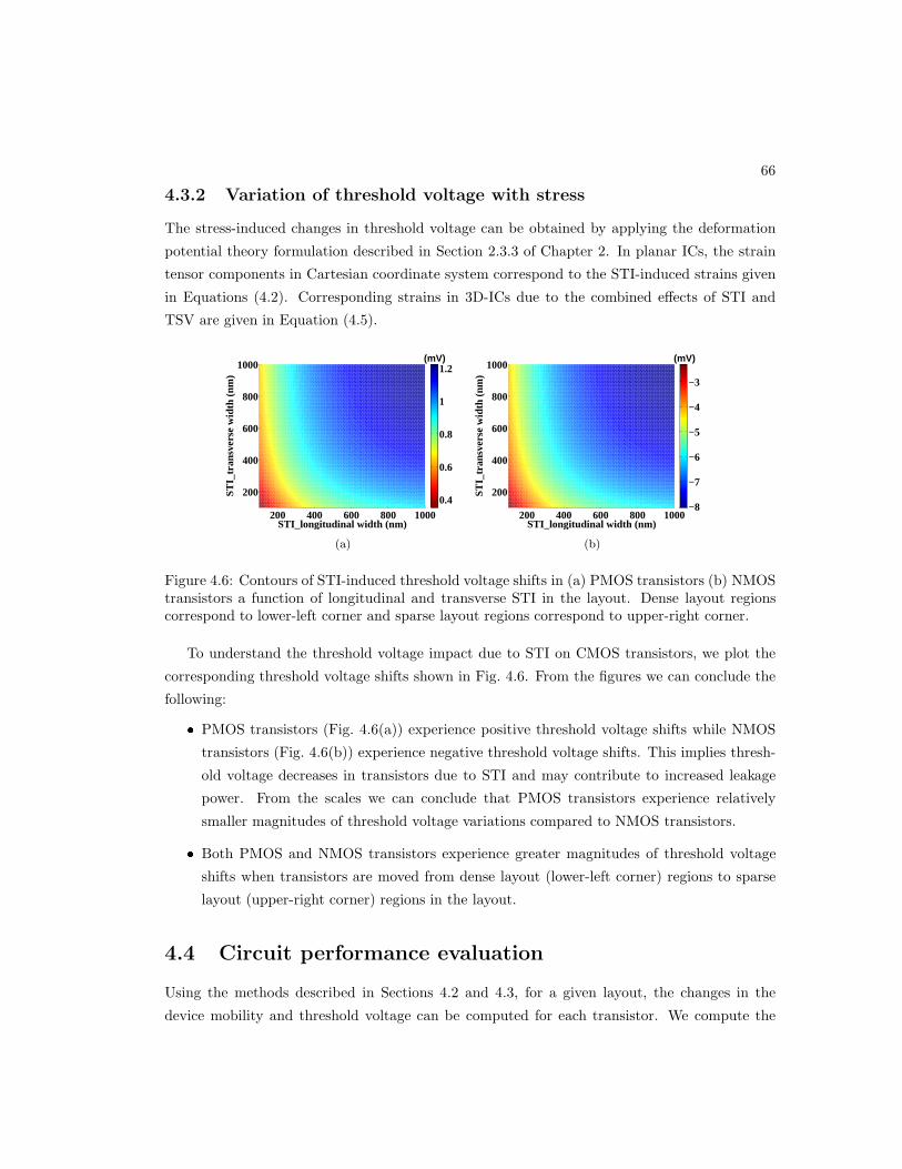
66
4.3.2 Variation of threshold voltage with stress
The stress-induced changes in threshold voltage can be obtained by applying the deformation
potential theory formulation described in Section 2.3.3 of Chapter 2. In planar ICs, the strain
tensor components in Cartesian coordinate system correspond to the STI-induced strains given
in Equations (4.2). Corresponding strains in 3D-ICs due to the combined effects of STI and
TSV are given in Equation (4.5).
200 400 600 800 1000
200
400
600
800
1000
STI_longitudinal width (nm)
ST
I_tr
ansv
erse
wid
th (
nm)
(mV)
0.4
0.6
0.8
1
1.2
(a)
200 400 600 800 1000
200
400
600
800
1000
STI_longitudinal width (nm)
ST
I_tr
ansv
erse
wid
th (
nm)
(mV)
−8
−7
−6
−5
−4
−3
(b)
Figure 4.6: Contours of STI-induced threshold voltage shifts in (a) PMOS transistors (b) NMOStransistors a function of longitudinal and transverse STI in the layout. Dense layout regionscorrespond to lower-left corner and sparse layout regions correspond to upper-right corner.
To understand the threshold voltage impact due to STI on CMOS transistors, we plot the
corresponding threshold voltage shifts shown in Fig. 4.6. From the figures we can conclude the
following: PMOS transistors (Fig. 4.6(a)) experience positive threshold voltage shifts while NMOS
transistors (Fig. 4.6(b)) experience negative threshold voltage shifts. This implies thresh-
old voltage decreases in transistors due to STI and may contribute to increased leakage
power. From the scales we can conclude that PMOS transistors experience relatively
smaller magnitudes of threshold voltage variations compared to NMOS transistors. Both PMOS and NMOS transistors experience greater magnitudes of threshold voltage
shifts when transistors are moved from dense layout (lower-left corner) regions to sparse
layout (upper-right corner) regions in the layout.
4.4 Circuit performance evaluation
Using the methods described in Sections 4.2 and 4.3, for a given layout, the changes in the
device mobility and threshold voltage can be computed for each transistor. We compute the

67
average of the electrical variations in the channel along the transistor width, and then evaluate
the variations in circuit performance by conducting static timing analysis and leakage power
analysis.
For a gate with n transistors, the delay under variations in the threshold voltage V strth,i and
mobility µstri for the ith transistor, 1 ≤ i ≤ n, can be computed using a first-order Taylor
expansion:
Dstr = D0 +
n∑
i=1
(
∂D
∂µi
∣
∣
∣
∣
0
∆µstri +∂D
∂Vth,i
∣
∣
∣
∣
0
∆V strth,i
)
(4.7)
where Dstr is the total gate delay due to STI+intentional stress in planar ICs or STI+intentional+TSV
stress in 3D-ICs. The term D0 denotes the nominal delay of the gate without any electrical vari-
ations, and the partial derivatives of delay with µi and Vth,i denote the delay sensitivity of the
gate to the mobility and threshold voltage, respectively, of transistor i, computed at the nominal
point.
The leakage power of a transistor exponentially increases (decreases) with its decreasing
(increasing) threshold voltage. However, for small changes in threshold voltage of a transistor,
the gate-level leakage power varies almost linearly. Threshold voltage variations in transistors
due to intentional and unintentional stresses are typically few tens of millivolts, while the nominal
threshold voltage of a transistor is about 400 mV in this work. Thus the leakage power of a gate
under unequal changes in threshold voltages of n transistors of a gate can also be computed
using a first order Taylor series expansion as:
Lstrgate = L0gate +
n∑
i=1
∂Lgate∂Vthi
∣
∣
∣
∣
0
∆V strthi (4.8)
where Lstrgate is the leakage power of a gate under STI-induced stress and L0gate is the nominal
leakage power of the gate under no stress. The partial derivative of Lgate with Vthi represents
the sensitivity of the leakage current of the gate to changes in the threshold voltage of transistor
i, evaluated at the nominal point. Our relative error in computing leakage power of standard
cells in this work is under 1%.
For a given placement, we use the analytical framework developed so far to compute the
circuit performance as follows: From the layout information for a circuit, we recover the STI configuration affecting the
transistors within each standard cell. We then compute the stress using the models in
Section 4.2. For the planar integrated circuits, the total stress for each STI configuration
is given by Equation (4.2). Similarly, for 3D-ICs, we use the superposition of stresses and
strains given in Equation (4.5). Based on the stress computations, we then proceed to compute the changes in mobility
and threshold voltage of each transistor using Equations (4.6) and (2.10), respectively.

68 Knowing the changes in electrical parameters of individual transistors in a logic gate, we
compute the delay and leakage power using Equations (4.7) and (4.8), respectively. We then perform static timing analysis and leakage computation.
4.5 Results
Shallow trench isolation effects on bulk planar transistors are highly layout-dependent. The
magnitude of electrical variation in a standard cell depends on its layout, and its relative po-
sition to its neighbours and their layouts. For 3D-IC circuits, the TSVs contribute additional
placement-dependent stress. We apply our methods on a set of IWLS benchmarks [58], listed in
Table 4.3, where H [W] represents the height [width] of the layouts, #PO denotes the number
of primary outputs, and D0 [L0] denotes the critical path delay [leakage power] without any
stress effects. We first describe the STI effects in conventional planar layouts and compare the
accuracy over prior works. We then present the combined contributions of TSV and STI for
3D-ICs.
Our standard cell layouts are based on the 45nm Nangate standard cell library [5]. The cells
consist of gates with single-, two-, and four-fingered layouts. The standard cells are characterised
for different load capacitances and input slopes at a supply voltage of 1.0V and a temperature
of about 25oC. Since STI is manufactured at 1000oC, it can be noted that the ∆T is almost the
same over the operating range of temperatures. From Chapter 3 we have seen that TSVs are
manufactured at 250oC. Although in principle TSV stress varies with operating temperature,
for ease of discussion we present the stress effects at 25oC alone.
We employ Capo [60] to obtain legalized placements of the IWLS circuits. For 3D-ICs
the TSVs are inserted in the planar layouts. It should be noted that relative placement of
the standard cells differ in the planar and 3D ICs. From the circuit placement information
and active layer information of the standard cell layouts, STI information is extracted as a
set of nonintersecting cuboids around the active region. We then employ our analytical stress
model from Section 4.2 to compute the stress in the active transistor regions. For 3D-IC circuit
placements, the TSV stress distributions from Section 3.2 are superposed onto the STI stress.
4.5.1 STI effects in planar integrated circuits
In the rest of the section, the STI along the active width [height] direction is termed as longitu-
dinal [transverse] STI. Tensile [compressive] stress indicates stress is positive [negative] valued.
Using the techniques in Section 4.4, we perform static timing analysis and leakage power analysis
on the circuits under three conditions: Nominal: STI effects in the layout are ignored.

69
Table 4.3: Characteristics of 45nm IWLS 2005 circuitsCkt. Index # Gates H×W # POs D0 L0
(µm×µm) (ps) (µW)ac97 ctrl C1 9047 92 × 171 4204 429 298aes core C2 11346 64 × 259 12313 418 226
des C3 4443 50 × 178 332 870 177ethernet C4 27060 184 × 242 32149 644 562
i2c C5 1110 23 × 76 204 389 35mem ctrl C6 8860 78 × 201 2522 842 251
pci bridge32 C7 9988 92 × 200 9025 636 325spi C8 3216 60 × 117 564 693 117
systemcdes C9 2600 48 × 119 549 694 118usb funct C10 10667 79 × 201 3930 624 248 3D STI: Our 3D stress model, superposing effects from STI rectangles in transverse and
longitudinal directions, is used. 1D STI: Only the effects of STI rectangles in the longitudinal direction are considered and
transverse effects are ignored.
Note that our 1D approach is more accurate than conventional 1D models which assume uni-
formity in the z direction, since it also considers finite depth effects along the z axis.
Table 4.4: Comparison of delay and leakage power under STI in planar ICsCkt. 3D STI 1D STI
∆D3D ∆L3D D+ ∆D+ D− ∆D− ∆D1D ∆L1D D− ∆D−
(%) (%) (ps) (%) (ps) (%) (%) (%) (ps) (%)C1 -5.3% 24.7% 108 15.7% 381 -8.7% -8.3% 16.9% 370 -11.9%C2 -3.9% 32.6% 173 2.9% 335 -9.6% -6.1% 26.5% 327 -12.5%C3 -4.1% 23.2% 354 2.0% 568 -8.1% -5.7% 15.8% 541 -11.3%C4 -2.2% 33.2% 434 1.6% 496 -8.9% -5.7% 26.6% 530 -12.3%C5 -6.6% 26.5% 192 10.4% 356 -9.0% -9.1% 18.7% 345 -12.5%C6 -5.2% 27.8% 473 1.3% 731 -8.1% -7.1% 20.6% 345 -12.5%C7 -3.7% 26.8% 350 1.1% 538 -11.5% -6.1% 18.5% 521 -15.2%C8 -2.2% 24.1% 476 2.7% 540 -8.1% -3.3% 17.0% 520 -12.5%C9 -2.1% 21.4% 458 2.6% 622 -5.0% -4.1% 14.2% 607 -7.6%C10 -4.3% 30.6% 289 1.7% 460 -8.3% -6.3% 23.4% 511 -10.4%
Table 4.4 shows the results under the 3D and 1D STI cases. The columns ∆D3D and ∆L3D
[∆D1D and ∆L1D] provide the changes in critical path delay and leakage power, respectively, in
the 3D STI [1D STI] case with respect to the nominal values, D0 and L0, from Table 4.3. Note
that the critical path may not be identical in the nominal circuit and the stressed circuit. Here,
positive [negative] changes denote increases [reductions] in the delay or leakage.
The above numbers only capture the delay changes in the worst-case path, where in all
cases, the delay happens to reduce for our benchmark set: between −2.1% and −6.6% for 3D
and between −3.3% and −9.1% for 1D. However, it is instructive to observe what happens
on noncritical paths by examining the largest delay shifts, over all paths in a circuit, from
the nominal to the stressed cases. Let D+ and D−, respectively, represent the delays (under
stress) of the paths in each circuit that show the largest delay increase and reduction. The

70
corresponding maximum delay increases and reductions observed on these paths are denoted by
∆D+ and ∆D−. Note that for the 1D STI case, we only show D− and ∆D− since only path
delay reductions are observed, and no increases are seen, i.e., ∆D+ is uniformly zero in 1D. On
the other hand, the value of ∆D+ varies from 1.1% to 15.7% for the 3D case. The values of
∆D− range from −5.0% to −11.5% for 3D, and are overestimated in 1D where they lie in the
range −7.6% to −15.2%.
To understand these results, we further analyze the 1D and 3D stress cases to explain the
observed trends in the data: When longitudinal STI is alone taken into account, as in the 1D case, the σx′x′ stress
component is provably always compressive, while σy′y′ is tensile. Furthermore, the mag-
nitude of σy′y′ is typically smaller than σx′x′ . Consequently in the 1D STI case, from
Equation (4.6) and the signs of π′11 and π′
12 in Table A.2, PMOS [NMOS] mobility always
improves [degrades]. When transverse STI effects are also considered, as in the 3D case, in the σx′x′ component
could be tensile or compressive, depending on the dimensions of the active region and the
STI, while σy′y′ is seen to be compressive in practice, as observed in Fig. 4.4. Thus, for
3D STI, the PMOS mobilities may improve or degrade, while NMOS mobilities always
degrade. Furthermore, the magnitudes of PMOS [NMOS] mobility variations in the 3D
STI case are smaller [greater] than the 1D STI case. In determining the impact of stress on circuit delay, STI-induced threshold voltage reduc-
tions attenuate [fortify] increases [reductions] in the mobility. While PMOS and NMOS
devices show similar levels of mobility shifts, the threshold voltage reductions for PMOS
are much lower than for NMOS. Therefore, PMOS devices are mostly mobility-dominated,
while NMOS device performance is determined by the balance between the shifts in mo-
bility and threshold voltage. This is reflected at the circuit level in terms of the increase
or reduction in path delays. Under STI effects, threshold voltages of both PMOS and NMOS transistors are lowered,
and the reduction depends on the amount of surrounding STI (which is higher in the 3D
case than the 1D case). Therefore, the leakage power is seen to increase from the nominal
case to either the 1D or 3D case. The shift the 3D STI [1D STI] formulation, ∆L3D [∆L1D]
can vary from 21.4% to 33.2% [14.2% to 26.6%]. Thus, when STI effects are neglected,
the leakage power can be significantly underestimated.
Layout guidelines: Based on the above analysis, for a given row-based placement, the following
guidelines are obtained:

71 To optimize delay, gates on critical/near-critical paths should have higher [smaller] lon-
gitudinal [transverse] spacing with respect to their neighbours in the same row [adjacent
rows]. To optimize leakage, noncritical gates should have minimum spacing with neighbours in
the row (longitudinal STI). Spaces in the rows above/below (transverse STI) should be
avoided.
4.5.2 Unintentional stress effects in 3D-ICs
.
In 3D-IC layouts employing TSVs, both STI- and TSV-induced stress effects cause circuit
performance variations. Using Capo placer, we generate a new set of layouts by inserting TSVs
in the layout. Note that the circuit placement dimensions are suitably increased to accommodate
TSVs. Similar to the description in Section 3.6, TSVs act as placement blockages. The attributes
of the TSV standard cells are: TSVs have a diameter of 5µm with SiO2 liner. The liner thickness is 125nm. TSV cells have a dimension of 7µÖ7µm and are placed 7µm apart.
The 3D-STI model is superposed with that of the TSV stress model as described in Sec-
tion 4.2.2 and Section 4.4. Table 4.5 shows the attributes of the three-dimensional integrated
circuit layouts along with stress-induced delay and leakage power variations. Here #TSV refers
to the number of TSVs in the circuit placement. The nominal delay and leakage power without
any stress effects are shown in columns D0 and L0 in Table 4.3. In Table 4.5, the delay variations
due to contributions from TSV alone, STI alone, and their combined contributions are given in
columns ∆DTSV , ∆DSTI , and ∆DComb. The corresponding leakage power variations are shown
in columns ∆LTSV , ∆LSTI , and ∆LComb. Positive (negative) changes indicate degradations
(improvements) in performance metrics. It should be noted that critical paths may be different
among the three cases.
From Table 4.5, the observed variations are summarized as follows: The delay variations considering TSV effects alone range from 2.5% to 12.5%. The corre-
sponding leakage power variations 2.4% to 5.1%. It can be observed that in the benchmarks
considered here, TSV effects cause delay and leakage power degradations. The ranges of delay and leakage power variations under STI effects alone are -3.3% to 3.7%
and 21.7% to 31.6%, respectively. It can be seen that STI effects cause both delay degrada-
tions and improvements. Moreover, the magnitudes of leakage power variations are greater
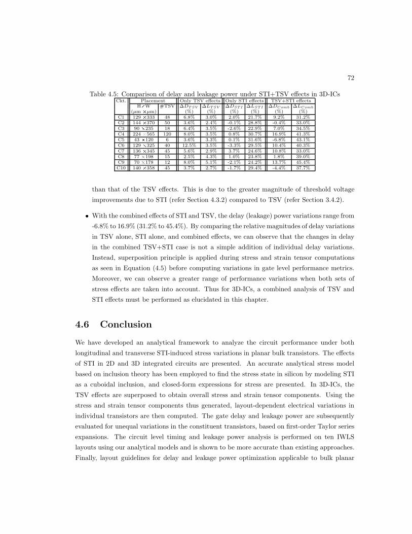
72
Table 4.5: Comparison of delay and leakage power under STI+TSV effects in 3D-ICsCkt. Placement Only TSV effects Only STI effects TSV+STI effects
HÖW #TSV ∆DT SV ∆LTSV ∆DST I ∆LSTI ∆DComb ∆LComb
(µm Öµm) (%) (%) (%) (%) (%) (%)C1 129 Ö333 48 6.8% 3.0% 2.0% 21.7% 9.2% 31.2%C2 144 Ö370 50 3.6% 2.4% -0.1% 28.8% -0.4% 33.0%C3 90 Ö235 18 6.4% 3.5% -2.6% 22.9% 7.0% 34.5%C4 224 Ö565 120 8.0% 3.5% 0.8% 30.7% 16.9% 41.3%C5 43 Ö120 6 3.6% 3.3% 0.1% 31.6% -6.8% 43.1%C6 129 Ö325 40 12.5% 3.5% -3.3% 29.5% 10.4% 40.3%C7 136 Ö345 45 5.6% 2.9% 3.7% 24.6% 10.8% 33.0%C8 77 Ö198 15 2.5% 4.3% 1.0% 23.8% 1.8% 39.0%C9 70 Ö178 12 8.0% 5.1% -2.1% 24.2% 13.7% 45.4%C10 140 Ö358 45 3.7% 2.7% -1.7% 29.4% -4.4% 37.7%
than that of the TSV effects. This is due to the greater magnitude of threshold voltage
improvements due to STI (refer Section 4.3.2) compared to TSV (refer Section 3.4.2). With the combined effects of STI and TSV, the delay (leakage) power variations range from
-6.8% to 16.9% (31.2% to 45.4%). By comparing the relative magnitudes of delay variations
in TSV alone, STI alone, and combined effects, we can observe that the changes in delay
in the combined TSV+STI case is not a simple addition of individual delay variations.
Instead, superposition principle is applied during stress and strain tensor computations
as seen in Equation (4.5) before computing variations in gate level performance metrics.
Moreover, we can observe a greater range of performance variations when both sets of
stress effects are taken into account. Thus for 3D-ICs, a combined analysis of TSV and
STI effects must be performed as elucidated in this chapter.
4.6 Conclusion
We have developed an analytical framework to analyze the circuit performance under both
longitudinal and transverse STI-induced stress variations in planar bulk transistors. The effects
of STI in 2D and 3D integrated circuits are presented. An accurate analytical stress model
based on inclusion theory has been employed to find the stress state in silicon by modeling STI
as a cuboidal inclusion, and closed-form expressions for stress are presented. In 3D-ICs, the
TSV effects are superposed to obtain overall stress and strain tensor components. Using the
stress and strain tensor components thus generated, layout-dependent electrical variations in
individual transistors are then computed. The gate delay and leakage power are subsequently
evaluated for unequal variations in the constituent transistors, based on first-order Taylor series
expansions. The circuit level timing and leakage power analysis is performed on ten IWLS
layouts using our analytical models and is shown to be more accurate than existing approaches.
Finally, layout guidelines for delay and leakage power optimization applicable to bulk planar

73
transistors are provided.
Chapter 5
Optimization of FinFET-based
circuits using a dual gate pitch
technique
Chapters 3 and 4 dealt with circuit performance variations due to unintentional stress in the
layout. In this chapter, we shall see how intentional stress in FinFETs depends upon layout
parameters. The engineered channel stresses due to source/drain stressors tend to relax along
the free edges of the FinFET and the magnitude of the stress depends upon the chosen gate
pitch of the design. In aggressively scaled technologies, the source/drain stressors tend to lose
their effectiveness due to smaller gate pitches. One way to reduce stress relaxation, as previously
proposed in the literature, is by using additional dummy gates at the ends of the standard cell.
However, it will be shown that using twice the gate pitch on selected standard cells in the design
results in better circuit performance.
This chapter is organized as follows. Section 5.1 gives a brief introduction to the layout-
dependent stress effects in FinFETs and shows how circuit performance improves with increas-
ing contacted gate pitch of the design. Section 5.2 introduces the FinFET structural and layout
parameters along with the stressors used in this work. Section 5.3 elaborates on the finite ele-
ment simulation methodology employed to simulate the process-induced stress. This is followed
by a discussion of the analytical techniques used to obtain mobility multipliers and threshold
voltage shifts, stored as a look-up-table, for standard cell characterization in Section 5.4. Fi-
nally, in Section 5.5, we use a sensitivity-based algorithm to improve the worst-case delay of
14nm/10nm/7nm benchmark circuits and compared our method with a similar gate sizing and
extra dummy approach.
74
75
5.1 Introduction
Modern lithography improves printability and reduces critical dimension (CD) variations by
requiring transistor gates in a standard cell to lie on a regular grid [74]. To achieve high
density, the contacted gate pitch (i.e., the minimum allowable distance between the centers
of two adjacent transistor gates with a contact in between) is typically set to be uniform.
In successive technology generations, this parameter is reduced to achieve higher integration
densities.
This notion of a constant pitch significantly impacts the performance of FinFETs [75] that
are used in advanced technologies to offer stronger control over short-channel effects and provide
higher on:off current ratios as compared to conventional planar transistors. As in planar tran-
sistors, FinFET performance can be greatly enhanced using strain engineering [17] by placing
stressors in the fin, in the source/drain region between the transistor gates. However, strain
engineering faces two difficulties in FinFET technologies: Reduced stressor volume: Reduced gate pitches imply that the volume of stressor in the
source/drain region is constrained, limiting the effectiveness of strain engineering [76]. Fin edge effects: Source/drain-induced stresses relax along the free edges at the end of
the fin [77], resulting in lower stresses and lower mobilities for transistors closer to the fin
edge.
To overcome the reduced stressor volume, i.e., the dependence of source/drain stressor volume
with contacted gate pitch, techniques such as densified STI [78], or metal-gate-induced stress
help to incorporate additional stress over and above source/drains stressors. Other methods
include a lattice-mismatched strain relaxed buffer that may be grown below the active fin, but
this is better suited for Ge-based fins and is impractical for silicon-based channels [76]. To
address fin edge effects, alternative layout topologies have been proposed, using fewer fins and
moving multi-fingered transistors toward the center of the fins [77]. The effectiveness of this
technique is limited to multi-finger gates with very short fins; it is inapplicable to minimum-sized
standard cells; therefore it does not provide significant improvements for many standard cells
in a library. Alternatively, multiple dummy gates may be added [79] at the ends of a fin (i.e.,
more than the single dummy gate that is normally used), thus moving the stress-relaxed end of
the fin away from the functional transistors; however, these dummy gates incur significant area
overheads. Furthermore, we show that the improvements due to multi-fingered transistors with
fewer fins and due to additional dummy gates diminish as the number of active gates increases.
On average, a standard cell in Nangate 15nm library [5] contains 6 transistor gates: altering the
layout topology and adding dummy gates provides improvements only for transistors near the

76
edge of the fin, but changing the contacted gate pitch can provide significant improvements in
strain for all transistors.
This work proposes using standard cells with with double the minimum contacted gate
pitch on selected gates that lie on critical paths, in order to improve the worst-case delay of
a circuit. Doubling the gate pitch increases the source/drain stressor volume and provides
greater mobility and threshold voltage improvements, but incurs about twice the area (standard
cell width), increased parasitic diffusion capacitance, and some increase in the leakage power.
However, it will be shown that the improvements in mobility and threshold voltage outweigh
the disadvantages when used selectively on the critical paths to optimize circuit delay. Since
only a few selected gates are modified to double gate pitch, the layout impact is not large, and
the area impact is further mitigated by the white space that is available in typical row-based
placements due to incomplete row utilization
Figure 5.1: Pull-up/pull-down transistors with nominal and double the gate pitch.
50 60 70 80 90 100 110100
120
140
160
180
200
Gate Pitch (nm)
Crit
ical
Pat
h D
elay
(ps
)
ac97_ctrlpci_bridge32
Figure 5.2: Changes in critical path delay with gate pitch under intentional stress variability fortwo benchmark circuits.
To illustrate the idea, Fig. 5.1 shows four-fin, two-gate structures with 1× (nominal) and
2× contacted gate pitch; these may represent a pull-up or pull-down network of a two-input
standard cell with a single dummy gate (in gray) at each end of the fin. An increase in the
contacted gate pitch increases the length of the green source/grain region between the gates,
where the stressors lie, and applies additional stress, enhancing performance. This reduces the
critical path delay, and its trend as a function of a uniform gate pitch (applied to every cell in
the layout), is illustrated in Fig. 5.2 for 14nm FinFET-based implementations of the ac97 ctrl

77
and pci bridge32 circuits. Here, the pitch is increased from the 1× (54nm) value to 2× (108nm)
in 9nm steps to illustrate the trend, but only 54nm and 108nm are legal values.
Our approach accounts for layout dependency [77] by characterizing stress in the underly-
ing layout and translating its impact on SPICE transistor model parameters. This is achieved
through a methodology that determines the stress on each transistor using FEM-based charac-
terizations, and storing the corresponding mobility multipliers and threshold voltage shifts as
a look-up-table. We use this to build and characterize a standard cell library with two ver-
sions of each cell, one with the standard gate pitch and one with twice the pitch. Finally, we
apply the notion of dual gate pitches to optimize benchmark circuits, comparing our approach
with conventional gate sizing, where selected gates on the critical paths are up-sized to improve
worst-case path delay.
5.2 FinFET parameters and stressors
The magnitude of engineered stress depends upon the FinFET geometry and layout parameters.
This section describes the FinFET structure and the intentional stressors considered in this work.
5.2.1 FinFET structure and layout
FinFET transistors belong to the family of three-dimensional multi-gate transistors, with the
gate wrapping around the channel on three sides. The structure is characterized by two sidewalls
and a top surface. If a hard mask exists on the top surface, it is treated as a double-gate
transistor, else it acts as a triple-gate transistor. We consider triple-gate transistor structures
in this work, but the concepts are applicable to double-gate FinFETs too.
(a) (b)
Figure 5.3: (a) Basic FinFET structure (b) Layout of a 4-fin-4-gate cell with dummy poly(dashed grey) at the ends.

78
A representative FinFET structure is shown in Fig. 5.3(a). The FinFET is characterized by
fin height, Hfin, fin thickness, Tfin, and gate length, Lgate. The electrical width, Wfin, for a
triple-gate structure is determined as Wfin = 2 × Hfin + Tfin. Often, multiple fins are used to
improve the drive current and to reduce variability of a given transistor. For a multi-fin device
with Nfin fins, the total electrical width is given as Nfin × Wfin, i.e., this can be increased in
quantized integer steps. The fin is partially surrounded by recessed shallow trench (STI) made
up of SiO2. We consider a Hi-K metal gate technology, where the Hi-K gate oxide is made up
of HfSiO, while the metal gate is made up of TiN metal.
In Fig. 5.3(b), the layout top-view of a four-fin four-transistor cell is shown. The gate is
flanked by a dielectric low-k spacer (yellow regions) of thickness LSP that reduces the gate-
to-source/drain capacitance. The terms Pgate and Pfin represent the gate pitch and fin pitch,
respectively. The length, LS/D, of the source/drain region can be derived from the primary
parameters as:
LS/D = Pgate − Lgate − 2 × LSP (5.1)
FinFET-based standard cells are flanked by a single dummy gates (shaded grey) at the end of
the fin, as shown in Fig. 5.3(b). Thus, for a given gate pitch Pgate, the width of a standard cell
with n active transistors, in the pull-up or pull-down network, is given as an integer multiple of
the gate pitch as (n + 1)Pgate. The FinFET structural and layout parameters used in this work
are given in Table 5.1.
Table 5.1: FinFET parametersLgate Hfin Tfin LSP Pfin Pgate
14nm 18nm 30nm 10nm 10nm 48nm 54nm
10nm 14nm 30nm 8nm 9nm 40nm 48nm
7nm 12nm 30nm 6nm 8nm 32nm 38nm
CMOS integrated circuits use logic gates typically with one to four independent inputs, and
the number of transistors in a minimum-sized gate is identical to the number of inputs. For
logic gates with higher drive strengths, fingered layouts are used. Here, we consider logic gates
of strengths 1Ö, 2Ö, and 4Ö, and for inverters or buffers (typically used to drive large loads), we
also consider 8Ö, 16Ö, and 32× standard cells. Therefore, in this paper, the number of active
transistors in a gate takes values NumTran ∈ 1, 2, 3, 4, 6, 8, 12, 16, 32.
5.2.2 Intentional stressors
Intentional stress can be engineered into transistor channels to boost mobilities and hence circuit
performance [17]. Positive (negative) valued stress is termed as tensile (compressive). For PMOS
(NMOS) transistor type a compressive (tensile) stress along the channel direction improves

79
the hole (electron) mobilities. The following state-of-the-art strain engineering techniques are
considered in this work: Source/drain stress: Lattice-mismatched SiGe (SiC) alloy is grown epitaxially in source/drain
regions to generate compressive (tensile) stress for PMOS (NMOS) transistors. Initial STI stress: Although regular STI is recessed below the channel and has minor
impact [17], using process techniques intrinsic compressive stresses in the range of GPa
can be developed in STI [78]. Initial gate stress: The metal gate can be incorporated with initial stresses that relax
to induce stress in the channel. An initial tensile (compressive) stress in the gate creates
compressive (tensile) stress in the channel [17].
We also assume the presence of one dummy gate at the edge of the fin. This generates some
compressive stress at the edge of the layout, instead of the stress relaxation that is seen in its
absence.
5.3 FinFET stress modeling and characterization
Post manufacturing, the lattice-mismatched stress in the source/drain regions, together with
the initial stresses in the STI and the metal gate relax and induce stress in the FinFET channel.
This section discusses the FEM-based stress modeling methodology that we develop for obtaining
stress distributions in the transistor channel in a standard cell layout.
In general, finite element simulations must be performed for all the standard cells in the
layout. However, recognizing structural similarities between the standard cells, we build a
set of stress primitives. For instance, the fin structure for logic gates INV X2, NAND2 X1,
and NOR2 X1 consists of the same number (two gates) of pull-up and pull-down transistors,
and they differ only in their electrical connectivity. We ignore the stress due to the contacts
whose contribution is negligible compared to other stressors [76]. Specifically, we perform stress
simulations to characterize fins with n ∈ NumTran gates and a dummy gate on each end, where
NumTran is as defined in Section 5.2.1.
5.3.1 Stress modeling
Finite element simulations are performed for various FinFET layout geometries using ABAQUS [30]
with the dimensions in Table 5.1 for each of the n ∈ NumTran gate structures for the 1×
(nominal) and 2× gate pitches. As seen from Section 2.2, the suitable coordinate system is the

80
primed coordinate system along the [110]-[110] axes. The corresponding notation for stress ten-
sor components are used here. The stresses in each transistor region are obtained by numerically
averaging the tensor components along fin width, fin height and channel length as:
σ′ =1
Lgate
1
Hfin
1
Tfin
∫
σ′dx′dy′dz (5.2)
The Young’s modulus (denoted by E) in GPa for the materials Si, SiO2, TiN, and HfSiO
are: 162, 71.7, 640, and 110, respectively. The corresponding Poisson’s ratio (denoted by ν) for
the materials Si, SiO2, TiN, and HfSiO are: 0.28, 0.16, 0.25, and 0.2.
5.3.2 Simulation of stress relaxation
The magnitude of the initial stress in lattice-mismatched source/drain regions depends upon the
mole fraction of the impurity (Ge or C) in the epitaxially grown alloy materials. For a Ge con-
centration of x% and C concentration of y%, the corresponding alloy materials are represented
as Si1−xGex and Si1−yCy, respectively. The lattice constants of Si, Ge, and C are 0.546nm,
0.566nm, and 0.347nm, respectively. The lattice constants of the alloy materials are obtained
by Vegard’s law which gives the resultant lattice constant as a linear combination of individual
lattice constants. Clearly, the lattice constant of Si1−xGex (Si1−yCy) is greater (smaller) than
the lattice constant of Si. In this work, we choose a Ge (C) concentration 50% (2%). Thus,
when the corresponding alloy materials are epitaxially grown in the source/drain regions, SiGe
has an initial compressive stress, while SiC is under a tensile stress in the neighbouring PMOS
and NMOS channels, respectively. Moreover, the stress thus developed is isotropic in nature.
The initial stress in the source/drain regions is computed as [16]:
SS/Dii =
ESi1 − 2νSi
(
aSi − aDaSi
)
d
Here, SS/Dii for i ∈ x′, y′, z denotes the initial stress component. The terms ESi and νSi represent
the Young’s modulus and Poisson’s ratio of silicon. The terms in the braces correspond to the
lattice-mismatched strain. The terms aSi and aD correspond to the lattice constants of silicon
and the impurity D ∈ Ge, C, respectively. The term d denotes the impurity concentration
and equals 50% for Ge, and 2% for C.
In addition, the compressive STI has an initial isotropic stress of SSTIii = −1GPa for i ∈
x′, y′, z. The corresponding initial stress in gate is Sgateii = +1GPa.
The gate-last approach is captured by a two-stage simulation: The system is first simulated with initial stresses of SS/Dii and SSTIii in the source/drain and
STI regions. Separate simulations are performed for tensile and compressive STI cases.
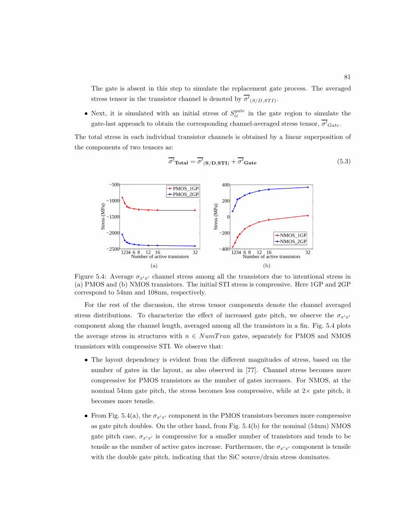
81
The gate is absent in this step to simulate the replacement gate process. The averaged
stress tensor in the transistor channel is denoted by σ′(S/D,STI). Next, it is simulated with an initial stress of Sgateii in the gate region to simulate the
gate-last approach to obtain the corresponding channel-averaged stress tensor, σ′Gate.
The total stress in each individual transistor channels is obtained by a linear superposition of
the components of two tensors as:
σ′Total = σ′
(S/D,STI) + σ′Gate (5.3)
1234 6 8 12 16 32−2500
−2000
−1500
−1000
−500
Number of active transistors
Str
ess
(MP
a)
PMOS_1GPPMOS_2GP
(a)
1234 6 8 12 16 32−400
−200
0
200
400
Number of active transistors
Str
ess
(MP
a)
NMOS_1GPNMOS_2GP
(b)
Figure 5.4: Average σx′x′ channel stress among all the transistors due to intentional stress in(a) PMOS and (b) NMOS transistors. The initial STI stress is compressive. Here 1GP and 2GPcorrespond to 54nm and 108nm, respectively.
For the rest of the discussion, the stress tensor components denote the channel averaged
stress distributions. To characterize the effect of increased gate pitch, we observe the σx′x′
component along the channel length, averaged among all the transistors in a fin. Fig. 5.4 plots
the average stress in structures with n ∈ NumTran gates, separately for PMOS and NMOS
transistors with compressive STI. We observe that: The layout dependency is evident from the different magnitudes of stress, based on the
number of gates in the layout, as also observed in [77]. Channel stress becomes more
compressive for PMOS transistors as the number of gates increases. For NMOS, at the
nominal 54nm gate pitch, the stress becomes less compressive, while at 2× gate pitch, it
becomes more tensile. From Fig. 5.4(a), the σx′x′ component in the PMOS transistors becomes more compressive
as gate pitch doubles. On the other hand, from Fig. 5.4(b) for the nominal (54nm) NMOS
gate pitch case, σx′x′ is compressive for a smaller number of transistors and tends to be
tensile as the number of active gates increase. Furthermore, the σx′x′ component is tensile
with the double gate pitch, indicating that the SiC source/drain stress dominates.
82
5.4 Stress-aware standard cell characterization
Having characterized the stress in a fin, we now focus on the impact of stress on electrical param-
eter variations in specific standard cells. In this section, we will present analytical mobility and
threshold voltage variation models based on analytical piezoresistivity and deformation poten-
tial theory, respectively. These models are used to populate look-up tables that determine the
mobility multipliers and threshold voltage shifts for each transistor within a standard cell [80],
which are fed to HSPICE simulations for library characterization.
5.4.1 Obtaining mobility multipliers and threshold voltage shifts
Mobility variations: In Section 2.3.1, we have seen the general model for piezoresistivity. Here
the transistor channels are taken to be along [110] Miller index direction along the wafer flat
direction. Thus φ′ = 0. Since FinFETs are three dimensional transistors all the three normal
stress components (σx′x′ , σy′y′ , σz′z′) are non-zero in the channel. The changes in mobility due
to the various intentional sources of mechanical stress is given by:
∆µk
µ= π′
11σkx′x′ + π′
12σky′y′ + π12σ
kz′z′ (5.4)
Here, µ denotes the carrier mobility and ∆µk the change in mobility in the kth transistor. The
terms π′11 and π′
12 are the piezoresistivity coefficients in the primed coordinate system, and
π12 is a piezoresistivity coefficient in the unprimed coordinate system since the z-axis remains
constant the translated coordinate system. The stress components σkx′x′ , σky′y′ , and σkz′z′ are the
channel averaged normal stress components in the kth transistor obtained from FEM simulations
outlined in Section 5.3.
The electrostatics in a FinFET transistor differ from bulk technology and so are their piezore-
sistivity coefficients. The piezoresistivity values for FinFET-based transistors are given in Ta-
ble A.4.
During SPICE-level simulations, the corresponding mobility multipliers in the transistor k
is given by 1 + ∆µk
µ .
Threshold voltage variations: Using the deformation potential theory models introduced
in Section 2.3.3, the changes in threshold voltage can be expressed a function of strain tensor
components in Cartesian coordinate system. For this, we transform the stress components from
finite element method using familiar stress-strain relations (Hooke’s Law) and axis transforma-
tions in [29]. The resultant changes in energy band potentials in the kth transistor of a standard

83
cell, with n ∈ NumTran transistors, are given as:
∆E(i)C(k)
= Ξd(
ǫkxx + ǫkyy + ǫkzz)
+ Ξuǫkii, i ∈ x′, y′, z′
∆E(hh,lh)V(k)
= a(
ǫkxx + ǫkyy + ǫkzz)
(5.5)
±
√
b2
4(ǫkxx + ǫkyy − 2ǫkzz)
2 +3b2
4(ǫkxx − ǫkyy)
2 + d2(
ǫkxy)2
Here, ∆E(i)C(k)
is the change in the conduction band potential energy in the carrier band i for the
kth transistor. The term EhhV(k)
(ElhV(k)
) denotes the heavy-hole [light-hole] valence band potential
of the kth transistor, with a corresponding usage of the positive [negative] sign in the expression.
The terms ǫkxx, ǫkyy, ǫkzz, ǫkyz, ǫkzx, and ǫkxy denote the six channel-averaged strain components of
the kth transistor in the Cartesian coordinate system. The coefficient terms Ξd and a are the
hydrostatic deformation potential constants and the terms Ξu, b, and d are the shear splitting
deformation potential constants. The corresponding values of the constants Ξd, Ξu, a, b, and d
in eV are 1.13, 9.16, 2.46, −2.35, and −5.08, respectively [2].
The threshold voltage of PMOS/NMOS transistors can in turn be expressed in terms of
changes in conduction band and valence band potentials as shown in Equation (2.10). In this
work, the changes in electronic band potentials are due to the source/drain, STI, and gate
stressors. The corresponding threshold voltage shifts in the kth transistor for a FinFET structure
with n ∈ NumTran transistors is given by:
q∆V kthp = (m − 1)∆EC(k)
− m∆EV(k)
q∆V kthn = −m∆EC(k)
+ (m − 1)∆EV(k)(5.6)
where ∆V kthp and ∆V k
thn are the threshold voltage shifts in PMOS and NMOS threshold voltages,
respectively, q is the electron charge, and m (= 1.3 – 1.4) is the body-effect coefficient. ∆EC(k)
is the minimum of the changes in conduction band potentials, ∆EiC(k)
and ∆EV(k)are the
maximum of the changes in valence band potentials, ∆EhhV(k)
and ∆ElhV(k)
of the kth transistor in
a standard cell.
Comparison: The Fig. 5.5 shows the mobility variations obtained by using Equation (5.4), and
the threshold voltage shifts obtained using Equation (5.6) for nominal and twice the gate pitch
in 14nm technology (Pgate = 54nm). From the figures we can deduce the following: From Fig. 5.5(a), we can see that the magnitudes of PMOS and NMOS mobility im-
provements are higher with double the gate pitch, consistent with observations in Fig. 5.4.
However, with 2× the gate pitch, the relative improvements in PMOS transistors is greater
than NMOS transistors and can be explained by the relative magnitudes of stress compo-
nents.

84
1234 6 8 12 16 32
−100
−50
0
50
100
Number of active transistors
Mob
ility
var
iatio
n (%
)
PMOS_1GPPMOS_2GPNMOS_1GPNMOS_2GP
(a)
1234 6 8 12 16 32−50
0
50
100
Number of active transistors
Thr
esho
ld v
olta
ge v
aria
tion
(mV
)
PMOS_1GPPMOS_2GPNMOS_1GPNMOS_2GP
(b)
Figure 5.5: (a) Average mobility (b) Average threshold voltage variations over all transistors inPMOS and NMOS FinFETs. Here 1GP and 2GP correspond to 54nm and 108nm, respectively. From Fig. 5.5(b), we can observe that the stress-induced threshold voltage shifts in PMOS
(NMOS) are positive (negative) valued indicating reduction in threshold voltages. More-
over, when gate pitch is doubled, PMOS and NMOS have increased threshold voltage
shifts. This contributes to delay improvements and increase in leakage power with 2×
gate pitch. Similar to mobility variations, the PMOS transistors experience higher magni-
tudes of threshold voltage shifts compared to NMOS transistors at double the gate pitch.
Incorporating shifts into BSIM-CMG [80]: The BSIM-CMG model provides two param-
eters, U0MULT and IDS0MULT, for modulating transistor current. The U0MULT parameter
affects the linear region alone, as it is coupled with other transistor parameters such as the satu-
ration drain voltage. In reality, due to applied stress, the saturation velocity is also boosted. The
current BSIM-CMG model allows only a single value for velocity saturation and it is not possible
to apply individual saturation velocity multipliers for the transistors. Hence we alternatively
use IDS0MULT to mimic the effect of stress-induced saturation current improvements. For the
threshold voltage shifts, the corresponding parameter in BSIM-CMG model is DELVTRAND.
5.4.2 Library characterization
The standard cell characterization takes the underlying layout into consideration. For a given
library of standard cells and their corresponding layouts, the following steps are performed
considering a nominal gate pitch and twice its value: We obtain stress distributions for different structures with n ∈ NumTran gates for nom-
inal and double the gate pitch. The stress tensor components are averaged along the
channel using Equation (5.2). We obtain the total stresses simulating gate-last approach
using Equation (5.3) in Section 5.3.2.

85 We obtain mobility variation and threshold voltage shifts by applying the piezoresis-
tivity model in Equation (5.4), and deformation potential theory formulation in Equa-
tions (5.5), (5.6). The electrical variations are stored in a look-up table as corresponding
mobility multipliers and as threshold voltage shifts. We apply, during standard cell characterization, based on the number of active transistors
in the layout, the look-up table entries by performing HSPICE circuit simulations. For delay, we characterize our standard cell library for different supply voltages, load
capacitances, and input slopes. For leakage power, we characterize our library for different
supply voltages and static input conditions.
We apply this standard cell characterization approach for a 14nm and 10nm PTM [59] technolo-
gies in conjunction with BSIM-CMG [81] FinFET transistor models. To allow standard cells
with twice the gate pitch to be used on selected gates of the critical paths, we characterize two
sets of libraries – one with nominal gate pitch, which we refer to as Library 1GP, and another
with twice the gate pitch which is referred to as Library 2GP. Thus it takes twice the time to
characterize both sets of libraries, but this is a one-time effort.
5.5 Results
In Sections 5.3 and 5.4, we have seen that using standard cells with twice the nominal gate pitch
improves the magnitudes of engineered mobility and threshold voltage shifts. In this section, we
show the circuit delay improvements that can be obtained by using standard cells with twice
the gate pitch. We compare our technique with conventional gate sizing approach and we show
that a combination of the two results in superior improvements.
5.5.1 Comparison of layout topologies
Before we present the layout optimization framework, we first compare the delay improvements
due to various topologies. Figure 5.6 shows five inverter layouts with various topologies. The
layouts are categorized as follows: Library 1GP layouts: The standard cells use nominal gate pitch with one pair of dummy
gates at the ends. The standard cell width of a n ∈ Ntran active transistors is given
by (n + 1)Pgate. Figures 5.6(a) and 5.6(b) belong to this library and correspond to a
minimum sized inverter and its higher strength variant, respectively. Library 2F layouts: For every standard cell in Library 1GP, the corresponding standard
cells in this library use multi-fingered layout with fewer fins. The corresponding standard

86
Figure 5.6: Layouts of (a) INV X1 (b) INV X2 (sizing) (c) INV X2 2F (multi-fingered layoutwith fewer fins) (d) INV X2 ExDummy (extra dummy gates) and (e) INV X1 2GP with twicethe gate pitch. For a gate pitch of 54nm, the corresponding standard cell widths are: 108nm,162nm, 162nm, 216nm and 216nm.
cell widths are given by (2n + 1)Pgate. Figure 5.6(c) shows the corresponding layout in
this library with respect to layout in Figure 5.6(a) of Library 1GP. Library ExDummy layouts: Every standard cell in this library uses an extra pair of dummy
gates. Figure 5.6(d) shows a 1× inverter in this library. The standard cell widths are given
b (n + 3)Pgate. Library 2GP layouts: The standard cells in this library use twice the gate pitch. Fig-
ure 5.6(e) shows a minimum sized inverter with twice the gate pitch. The standard cell
widths can be deduced as 2(n + 1)Pgate.
INV_X1 INV_X2 INV_X4 INV_X80
0.5
1
1.5
2
Nor
mal
ized
RO
−de
lay
Library_1GPLibrary_2FLibrary_ExDummyLibrary_2GP
Figure 5.7: Comparison of ring oscillator delays for different inverters under intentional stressvariability. The corresponding number of fingers in INV X1, INV X2, INV X4, and INV X8inverters are 1, 2, 4, and 8. The ring-oscillator delays are normalized to Library 1GP ring-oscillator.

87
We construct 17-stage ring oscillators with FO4 load with inverters from each of the above
libraries. Four ring oscillators are built in each library with inverter-stages corresponding to
INV X1 (1-finger layout), INV X2 (2-finger layout), INV X4 (4-finger layout), INV X8 (8-finger
layout). This is to mimic the number of active transistors in the layout. The ring oscilla-
tor in Library 1GP are taken as reference and the relative delay improvements with layouts
from the other three libraries are shown in Figure 5.7. From the figure, we can conclude that
compared to all three layout topologies, using twice the gate pitch gives best delay improve-
ments. Furthermore, we can see that the relative improvements in using Library 2F [77] and
Library ExDummy [79] diminish with the number of fingers (active transistors) in the layout.
We shall thus confine our optimization framework to standard cells from Library 1GP and Li-
brary 2GP alone.
5.5.2 Timing optimization framework
We begin with a placed circuit netlist with nominal gate pitch, and apply optimization techniques
to improve the delay by replacing selected standard cells with twice the gate pitch or by using
a higher strength variant (sizing) of the standard cell. For this we chose a TILOS [82] based
circuit optimization framework. We find the best delay achievable with our optimization within
the given placement area. Typical standard cell rows have enough white space to accommodate
the higher strength variants or the double gate pitch variants; for example, our benchmarks
show row utilizations ranging from 35% to 80%. The timing optimization is outlined as follows:
I. Find the current most critical path in the design.
II. For each gate on the current critical path, compute the change in the critical path de-
lay, ∆D, and leakage power, ∆L, obtained by either upsizing the gate or by choosing a
corresponding gate with twice the gate pitch.
III. Find the gate with the best gain G = ∆D/∆L, and replace it with corresponding higher
strength variant (sizing) or with a corresponding standard cell with twice the gate pitch.
IV. Go to step I till convergence criteria is met.
The procedure converges when no possible upsizing/double gate pitch standard cells are
found, or if the circuit area exceeds a bound. We compare three strategies for circuit optimiza-
tion: Only gate sizing (OPT X): The cells are replaced by an upsized variant, e.g., INV X1 may
be replaced with INV X2 (Fig. 5.6). The cells are chosen from Library 1GP alone.

88 Only double gate pitch (OPT 2GP): The cells are replaced are corresponding cells with
twice the gate pitch, e.g., INV X1 may be replaced with INV X1 2GP (Fig. 5.6). The cells
are chosen from Library 2GP alone. Combined optimization (OPT Comb): While selecting the cell with best gain, we consider
both sizing and double gate pitch options, and chose the cell with a higher gain. Cells can
be chosen from either Library 1GP or Library 2GP.
Gate selection: We now show a example of gate choices during optimization. Table 5.2 shows
the delay and average leakage power of a set of NAND2 standard cells in the Library 1GP,
Library ExDummy, and Library 2GP. The standard cells in Library 1GP and Library 2GP have
nominal and twice the gate pitch, respectively as discussed in Section 5.4.2. The gates in
Library ExDummy have an additional pair of dummy gates so that the active transistors do not
experience fin-edge effects. The column n denotes the number of active transistors in the fin.
We can see that a higher strength variant within the same library provides both superior PMOS
rise and NMOS fall delays, while the corresponding cell with twice the gate pitch provides better
PMOS rise-delay improvements compared to NMOS fall-delay improvements. This is due to the
relatively smaller mobility and threshold voltage improvements in NMOS transistors shown in
Fig. 5.5 in Section 5.4.1. The standard cell leakage power is expected to increase with increased
width (higher strength) and with greater threshold voltage shifts (twice the gate pitch). However,
doubling the gate pitch incurs comparatively smaller magnitude of leakage power compared to
upsizing a gate. Further, it can be seen that the best rise delay improvement from the 2GP case is
significantly better than that of the 1GP case. For completeness, we compare the corresponding
gates in the Library ExDummy. We can observe that the delay improvements, obtained by
adding additional dummy gates, diminish with the number of active transistors.
Table 5.2: Delay and leakage power of 14nm NAND2 cells.
Gate nLibrary 1GP Library ExDummy Library 2GP
Rise/Fall Leakage Rise/Fall Leakage Rise/Fall Leakage(ps) (nW) (ps) (nW) (ps) (nW)
NAND2 X1 2 11.4/19.4 19.9 11.2/16.9 20.5 7.1/18.7 32.2NAND2 X2 4 7.6/13.1 40.2 6.7/12.3 40.8 3.9/12.7 64.7NAND2 X4 8 6.1/10.7 80.8 6/10.6 81 3.2/9.2 130.3
5.5.3 Circuit-level optimization with dual gate pitches
We apply our techniques to a set of IWLS05 [58] benchmarks described in Table 5.3. The column
denoted #G refers number of number of gates in the corresponding circuit. We use CAPO [60]
for circuit placement and PTM SPICE models. Our inputs are:

89
Table 5.3: Circuit optimization results using conventional gate sizing and dual gate pitch tech-niques for 14nm technology
Circuit #G
14nm TechnologyNominal OPT X OPT 2GP OPT Comb
D0 P0 E0 ∆D1 ∆P1 ∆E1 ∆D2 ∆P2 ∆E2 ∆D3 ∆P3 ∆E3
(Ö1K) (ps) (µW) (fJ) (%) (%) (%) (%) (%) (%) (%) (%) (%)ac97 ctrl 9.5 131 845 111 -20.6% 2.0% -19.0% -18.3% 1.31% -17.2% -22.1% 2.8% -20.0%aes core 11.9 141 700 99 -9.9% 1.2% -8.9% -11.3% 1.34% -10.2% -18.4% 3.0% -16.0%des 4.6 264 463 122 -3.0% 0.3% -2.8% -8.7% 0.27% -8.5% -9.8% 1.3% -8.7%ethernet 28.0 238 1704 406 -6.7% 0.3% -6.5% -8.0% 0.33% -7.7% -11.3% 0.6% -10.8%i2c 1.0 134 87 12 -18.7% 2.1% -16.9% -11.9% 0.98% -11.1% -24.6% 6.4% -19.8%mem ctrl 8.9 253 707 179 0.0% 0.01% 0.01% -6.7% 0.34% -6.4% -9.5% 1.2% -8.4%pci bridge32 10.0 187 727 136 -9.6% 0.7% -9.0% -13.4% 1.10% -12.4% -17.1% 1.7% -15.7%spi 3.1 259 262 68 -15.4% 0.8% -14.7% -5.0% 0.18% -4.9% -17.4% 1.6% -16.1%systemcdes 2.7 208 275 57 -2.4% 0.2% -2.2% -6.3% 0.37% -5.9% -9.1% 0.8% -8.4%usb funct 11.2 192 749 144 -1.6% 0.1% -1.4% -10.4% 0.46% -10.0% -5.7% 0.5% -5.3%
Average -8.8% 0.8% -8.1% -10.0% 0.7% -9.4% -14.5% 2.0% -12.9% Characterized standard cell libraries with nominal (Library 1GP) and double gate pitch
(Library 2GP) for 14nm/10nm technology. An initial placed netlist with nominal gate pitch cells. We treat this as our reference and
term it as the “Nominal” case. Note that the layouts of 14nm and 10nm are different.
Table 5.4: Circuit optimization results using conventional gate sizing and dual gate pitch tech-niques for 10nm technology
Circuit Nominal OPT X OPT 2GP OPT CombD4 E4 ∆D5 ∆E5 ∆D6 ∆E6 ∆D7 ∆E7
(ps) (fJ) (%) (%) (%) (%) (%) (%)ac97 ctrl 103 94 -19.4% -18.2% -28.2% -26.3% -29.1% -26.5%aes core 101 77 -7.9% -7.0% -6.9% -6.1% -14.9% -12.1%des 206 103 -11.7% -11.1% -15.5% -14.9% -15.5% -14.3%ethernet 206 373 -8.3% -7.9% -3.9% -3.8% -6.8% -6.6%i2c 120 11 -32.5% -30.6% -36.7% -34.0% -41.7% -37.2%mem ctrl 203 153 -6.4% -6.1% -5.4% -5.2% -10.8% -9.8%pci bridge32 149 117 -14.1% -13.2% -14.8% -13.9% -19.5% -18.1%spi 213 60 -6.1% -5.8% -6.6% -6.3% -19.2% -17.9%systemcdes 166 49 0.0% 0.02% -13.9% -12.9% -9.0% -8.6%usb funct 146 117 -13.7% -12.9% -8.2% -7.8% -8.9% -8.4%
Average -12.0% -11.3% -14.0% -13.1% -17.5% -15.9%
We run static timing analysis and compute the dynamic and static leakage power by propa-
gating signal probabilities. We compare the delay, total power, and the power-delay product of
the nominal and timing-optimized circuits, where the power-delay product multiplies the total
power and the worst-case path delay of the circuit, and is a measure of the energy consumption
per clock cycle.
The results of the three optimizations, OPT X, OPT 2GP, and OPT Comb are obtained for
14/10/7 nm technologies. Tables 5.3, 5.4, and 5.5 present the corresponding results for 14nm,
10nm, and 7nm technologies, respectively. In Table 5.3, the columns D0, P0, and E0 denote
the worst-case critical path delay, total power (sum of dynamic and static leakage power), and

90
Table 5.5: Circuit optimization results using conventional gate sizing and dual gate pitch tech-niques for 7nm technology
Circuit Nominal OPT X OPT 2GP OPT CombD8 E8 ∆D9 ∆E9 ∆D10 ∆E10 ∆D11 ∆E12
(ps) (fJ) (%) (%) (%) (%) (%) (%)ac97 ctrl 141 12 -24.1% -13.1% -24.1% -13.1% -28.4% -14.9%aes core 133 13 -5.3% -1.9% -10.5% -3.9% -19.5% -6.5%des 256 10 -3.9% -2.6% -12.1% -8.3% -21.9% -14.7%ethernet 247 33 -20.2% -14.4% -21.5% -15.2% -26.3% -18.6%i2c 160 1 -42.5% -25.6% -35.6% -21.1% -55.0% -30.9%mem ctrl 270 16 0.0% 0.0% -5.6% -3.9% -11.9% -8.1%pci bridge32 185 13 -8.1% -4.5% -11.4% -6.4% -17.8% -9.8%spi 257 6 -16.0% -10.9% -21.8% -14.8% -21.8% -14.1%systemcdes 198 5 0.0% 0.00% -9.6% -5.9% -11.1% -6.8%usb funct 191 14 -11.0% -6.5% -20.9% -12.2% -21.5% -12.5%
Average -13.1% -7.9% -17.3% -10.5% -23.5% -13.7%
the power-delay product of the nominal circuit without optimizations in 14nm technology. We
present the changes in the circuit metrics with reference to the nominal case. The columns
∆Di, ∆Pi, and ∆Ei under 14nm technology indicate the changes in delay, total power, and
the power-delay product using optimization i, where i = 1, 2, 3 refer to OPT X, OPT 2GP, and
OPT Comb, respectively. In Table 5.4, for 10nm technology, the columns D4 and E4 denote
the nominal delay and power-delay product, respectively. The relative changes in delay (power-
delay product) for OPT X, OPT 2GP, and OPT Comb are given in columns ∆D5, ∆D6, and
∆D7 (∆E5, ∆E6, and ∆E7), respectively. In Table 5.5, for 7nm technology, the columns D8
and E8 represent the nominal delay and power-delay product, respectively. The corresponding
relative changes in delay (power-delay product) for OPT X, OPT 2GP, and OPT Comb are
given in columns ∆D9, ∆D9, and ∆D10 (∆E10, ∆E11, and ∆E11). Negative (positive) changes
indicate improvements (degradations). It can be seen that the total power increases for all the
optimizations. This is because, a higher strength variant has greater transistor width, while
using cells with twice the gate pitch incurs higher magnitudes of threshold voltage shifts as seen
in Fig. 5.5. Both these effects contribute to increased leakage power of the circuit. Finally, we
report the average improvements (degradations) in delay and power-delay product (total power)
for all optimizers, over all circuits.
From Table 5.3 (Table 5.4 and Table 5.5), the corresponding changes in circuit metrics using
the three optimization techniques in 14nm technology (10nm and 7nm technologies, respectively)
are summarized as follows: OPT X: For 14nm technology, the delay improvements range from 0% to 20.6%, the total
power degrades by 0.01% to 2.11%, and the power-delay product changes by -18.99% to
0.01%. We can observe that for the benchmark mem ctrl in this work, the critical path
delay did not change but the total power increases by 0.01% (however, the critical paths
before and after optimization are different); for the remaining circuits, we can observe

91
improvements in delay and the power-delay product. The average improvements in delay
and power-delay product are -8.8% and -8.1%, respectively. For 10nm technology, the
ranges of (average) delay and power-delay product improvements are: -32.5% to 0% (-
12%), and -3.8% to -34% (-11.3%), respectively. For 7nm technology, the corresponding
ranges of (average) delay and power-delay product improvements are: 0% to -42.5% (-
13.1%), and -25.6% to 0.01% (-7.9%). OPT 2GP: For 14nm technology, the delay and power-delay improvements range from -5%
to -18.3% and -4.9% to -17.2%, respectively, for a total power overhead ranging from 0.18%
to 1.34%. The corresponding average improvements in delay and power-delay product
are -10% and -9.4%. For 10nm technology, the ranges of (average) delay and power-
delay product improvements are: -3.9% to -36.7% (-14%), and -30.64% to 0.02% (-13.1%),
respectively. For 7nm technology, the corresponding ranges of (average) delay and power-
delay product improvements are:-5.6% to -35.6% (-17.3%), and -3.9% to -21.1% (-10.5%). OPT Comb: For 14nm technology, the changes in delay, total power, and power-delay
product range are: -5.7% to -24.6%, 0.49% to 6.37%, and -5.3% to -20%, respectively. The
average delay and power-delay product improvements are -14.5% and -12.9%, respectively.
For 10nm technology, the corresponding ranges (average) of delay and power-delay product
improvements are: -32.5% to 0% (-17.5%), and -3.8% to -34% (-15.9%). For 7nm technol-
ogy, the corresponding ranges of (average) delay and power-delay product improvements
are:-11.1% to -55% (-17.3%), and -6.5% to -30.9% (-13.7%).
From the changes in circuit metrics, we can observe that the performance of the dual gate
pitch technique (OPT 2GP) is superior to the only sizing approach (OPT X) in most of the cir-
cuits except ac97 ctrl, i2c, and spi (ethernet, mem ctrl and usb funct) in 14nm (10nm) circuits.
In 7nm technology, the OPT 2GP is superior to OPT X in most circuits except ac97 ctrl and i2c
circuits. The relatively smaller delay improvements due to OPT 2GP approach in these circuits,
is due to the smaller NMOS fall delays improvements compared to PMOS rise delays as discussed
in Section 5.5.2. On the other hand the use of sizing can improve both the rise/fall delays of
a given gate on the critical path. This shows that it is worth exploring the possibility of using
a combination of both the techniques as demonstrated by the combined approach. In fact, on
an average, the OPT Comb optimization approach provides better delay and power-delay prod-
uct improvements. In addition, it was observed that the OPT Comb approach predominantly
chooses corresponding cells from Library 2GP (2× gate pitch) over higher strength variants in
LIbrary 1GP owing to their superior rise delay improvements at a considerably smaller leakage
overhead (refer Section 5.5.2).
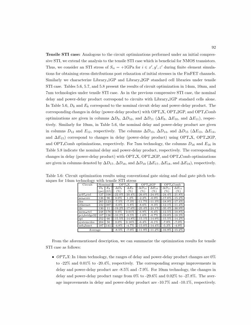
92
Tensile STI case: Analogous to the circuit optimizations performed under an initial compres-
sive STI, we extend the analysis to the tensile STI case which is beneficial for NMOS transistors.
Thus, we consider an STI stress of Sii = +1GPa for i ∈ x′, y′, z′ during finite element simula-
tions for obtaining stress distributions post relaxation of initial stresses in the FinFET channels.
Similarly we characterize Library 1GP and Library 2GP standard cell libraries under tensile
STI case. Tables 5.6, 5.7, and 5.8 present the results of circuit optimization in 14nm, 10nm, and
7nm technologies under tensile STI case. As in the previous compressive STI case, the nominal
delay and power-delay product correspond to circuits with Library 1GP standard cells alone.
In Table 5.6, D8 and E8 correspond to the nominal circuit delay and power-delay product. The
corresponding changes in delay (power-delay product) with OPT X, OPT 2GP, and OPT Comb
optimizations are given in columns ∆D9, ∆D10, and ∆D11 (∆E9, ∆E10, and ∆E11), respec-
tively. Similarly for 10nm, in Table 5.6, the nominal delay and power-delay product are given
in columns D12 and E12, respectively. The columns ∆D13, ∆D14, and ∆D15 (∆E13, ∆E14,
and ∆E15) correspond to changes in delay (power-delay product) using OPT X, OPT 2GP,
and OPT Comb optimizations, respectively. For 7nm technology, the columns D16 and E16 in
Table 5.8 indicate the nominal delay and power-delay product, respectively. The corresponding
changes in delay (power-delay product) with OPT X, OPT 2GP, and OPT Comb optimizations
are given in columns denoted by ∆D17, ∆D18, and ∆D19 (∆E17, ∆E18, and ∆E19), respectively.
Table 5.6: Circuit optimization results using conventional gate sizing and dual gate pitch tech-niques for 14nm technology with tensile STI stress
Circuit Nominal OPT X OPT 2GP OPT CombD8 E8 ∆D9 ∆E9 ∆D10 ∆E10 ∆D11 ∆E11
(ps) (fJ) (%) (%) (%) (%) (%) (%)ac97 ctrl 127 108 -22.0% -20.4% -26.0% -24.9% -24.4% -21.8%aes core 136 96 0.0% 1.2% -2.2% -0.9% -17.6% -15.2%des 265 123 -7.5% -7.3% -11.7% -11.3% -18.9% -17.4%ethernet 232 397 -6.0% -5.8% -8.6% -8.3% -12.1% -11.4%i2c 130 11 -19.2% -17.6% -25.4% -24.1% -35.4% -30.9%mem ctrl 248 176 0.0% 0.01% -6.9% -6.4% -12.5% -10.8%pci bridge32 187 136 -10.2% -9.5% -1.6% -0.7% -19.8% -18.3%spi 252 66 -15.5% -14.8% -15.1% -14.9% -15.5% -14.2%systemcdes 204 56 0.0% 0.16% -6.4% -6.1% -7.8% -7.0%usb funct 187 141 -4.8% -4.7% -15.0% -14.4% -5.3% -4.9%
Average -8.5% -7.9% -11.9% -11.2% -16.9% -15.2%
From the aforementioned description, we can summarize the optimization results for tensile
STI case as follows: OPT X: In 14nm technology, the ranges of delay and power-delay product changes are 0%
to -22% and 0.01% to -20.4%, respectively. The corresponding average improvements in
delay and power-delay product are -8.5% and -7.9%. For 10nm technology, the changes in
delay and power-delay product range from 0% to -29.6% and 0.02% to -27.8%. The aver-
age improvements in delay and power-delay product are -10.7% and -10.1%, respectively.

93
Table 5.7: Circuit optimization results using conventional gate sizing and dual gate pitch tech-niques for 10nm technology with tensile STI stress
Circuit Nominal OPT X OPT 2GP OPT CombD12 E12 ∆D13 ∆E13 ∆D14 ∆E14 ∆D15 ∆E15
(ps) (fJ) (%) (%) (%) (%) (%) (%)ac97 ctrl 102 94 -12.7% -11.9% -24.5% -22.9% -22.5% -21.0%aes core 97 75 -6.2% -5.4% -7.2% -6.4% -14.4% -11.4%des 205 102 -10.7% -10.1% -15.1% -14.6% -15.6% -14.5%ethernet 204 371 -9.8% -9.4% -3.4% -3.3% -6.4% -6.2%i2c 115 11 -29.6% -27.8% -36.5% -33.7% -42.6% -36.5%mem ctrl 197 150 -4.1% -3.8% -7.1% -6.8% -12.2% -10.1%pci bridge32 149 117 -19.5% -18.2% -15.4% -14.6% -22.1% -20.5%spi 210 60 -5.7% -5.4% -6.2% -5.9% -20.0% -18.6%systemcdes 165 49 0.0% 0.02% -17.0% -15.7% -9.1% -8.6%usb funct 144 116 -9.0% -8.5% -5.6% -5.3% 0.0% 0.01%
Average -10.7% -10.1% -13.8% -12.9% -16.5% -14.8%
Table 5.8: Circuit optimization results using conventional gate sizing and dual gate pitch tech-niques for 7nm technology with tensile STI stress
Circuit Nominal OPT X OPT 2GP OPT CombD16 E16 ∆D17 ∆E17 ∆D18 ∆E18 ∆D19 ∆E19
(ps) (fJ) (%) (%) (%) (%) (%) (%)ac97 ctrl 137 12 -25.5% -13.8% -34.3% -18.5% -38.7% -20.3%aes core 124 13 -2.4% -0.8% -7.3% -2.6% -17.7% -5.5%des 257 10 -9.3% -6.4% -19.8% -13.6% -22.6% -14.6%ethernet 227 32 -15.0% -10.4% -16.7% -11.6% -21.6% -14.9%i2c 146 1 -43.2% -24.5% -33.6% -19.1% -41.8% -24.2%mem ctrl 254 15 -4.3% -2.9% -7.9% -5.4% -13.4% -8.6%pci bridge32 177 13 -14.7% -8.0% -10.7% -5.9% -21.5% -11.4%spi 251 6 -15.1% -10.2% -17.9% -12.1% -18.7% -12.1%systemcdes 195 5 -1.5% -0.91% -9.2% -5.5% -9.2% -5.6%usb funct 190 14 0.02% 0.02% -21.1% -12.3% -20.0% -11.62%
Average -13.1% -7.8% -17.9% -10.7% -22.5% -12.9%
In 7nm technology, the ranges in delay and power-delay product are 0.02% to -43.2%
and 0.02% to -24.5%, respectively. The average improvements in delay and power-delay
product are -13.1% and -7.8%, respectively. OPT 2GP: In 14nm technology, the ranges of delay and power-delay product changes are
-1.6% to -26% and -0.7% to -24.9%, respectively. The corresponding average improve-
ments in delay and power-delay product are -11.9% and -11.2%. For 10nm technology,
the changes in delay and power-delay product range from -3.4% to -36.5% and -3.3% to
-33.7%. The average improvements in delay and power-delay product are -13.8% and -
12.9%, respectively. In 7nm technology, the ranges in delay and power-delay product are
-7.3% to -34.3% and -2.6% to -19.1%, respectively. The average improvements in delay
and power-delay product are -17.9% and -10.7%, respectively. OPT Comb: In 14nm technology, the ranges of delay and power-delay product changes are
-5.3% to -35.4% and -4.9% to -30.9%, respectively. The corresponding average improve-
ments in delay and power-delay product are -16.9% and -15.2%. For 10nm technology,

94
the changes in delay and power-delay product range from 0% to -42.6% and 0.01% to
-36.5%. The average improvements in delay and power-delay product are -16.5% and -
14.8%, respectively. In 7nm technology, the ranges in delay and power-delay product are
-9.2% to -41.8% and -5.5% to -24.2%, respectively. The average improvements in delay
and power-delay product are -22.5% and -12.9%, respectively.
Similar to compressive STI case, OPT 2GP performs superior to OPT X case in most of
the circuits. The deviations if any can similarly be attributed to the improvements in both
NMOS and PMOS delays due to upsizing (OPT X) compared to OPT 2GP approach. From
the observations, we can observe that even with tensile STI as initial stress, the OPT Comb
optimization provides the best improvements in delay and power-delay product on an average.
Thus, we can conclude that using a dual gate pitch technique in combination with conventional
sizing approach leads to improvement in delay and power-delay product of FinFET-based circuits
under both compressive and tensile STI conditions.
5.6 Conclusions
This work demonstrates a dual gate pitch technique to improve the source/drain stressor effec-
tiveness in FinFET-based circuits. A dual gate pitch technique is proposed, where selected gates
on the critical path are be replaced with corresponding gates with twice the gate pitch. The
stress distributions in the FinFETs are obtained through FEM simulations, and subsequently
used to generate look-up tables for mobility multipliers and threshold voltage shifts at SPICE
level. A sensitivity-based circuit optimization is employed to optimize circuit delays using siz-
ing, twice the gate pitch, and a combination of both the techniques. The techniques have been
demonstrated for both compressive and tensile STI case. It has been shown that the power-delay
product of FinFET-based circuits can be improved by performing a concurrent sizing and dual
gate pitch optimization.

Chapter 6
Conclusions
From the previous chapters we have observed that unintentional stress in the layout cause
changes in transistor mobility and threshold voltage which in turn affect circuit-level performance
metrics. It was also observed that the magnitudes of stress depends upon the relative location
of the transistors with that of stressors in the layout. Chapters 3 and 4 dealt with capturing
performance variations due to unintentional stresses from TSV and STI, respectively in the
layout. On the other hand, Chapter 5 studied the effects of intentional stress variation with
layout parameters in FinFETs. Using the modeling paradigm, we have been able to quantify
the effects of the variations on circuit timing behavior and leakage power. This enabled us to
optimize the circuit layout to improve performance.
Specifically, in Chapter 3, an analytical stress model was developed for TSV-induced stress
distributions in 3D-ICs using 2D axisymmetric and Boussinesq type solutions in linear elasticity.
The stress model was shown to be accurate with FEM. The stress distributions were then
converted to mobility and threshold voltage variations in transistors using piezoresistivity and
deformation potential theory models, respectively. The changes in electrical parameters were
then used to predict the delay and leakage power of the logic cells during circuit analysis.
A thorough path delay analysis was performed using the techniques. It was concluded that
the magnitude of performance variations in transistors depends upon the relative locations of
the transistors and TSVs in the layout. Finally, based on our modeling techniques, we have
established a set of layout guidelines to improve circuit delay.
Chapter 4 developed a framework to analyze the effects of shallow trench isolation on circuit
performance in planar ICs and 3D-ICs. We employed modeling techniques from micromechanics
based on inclusion theory to obtain accurate stress distributions due to surrounding STI in the
layout. The stress and strain tensor components were then translated to mobility and threshold
voltage, using piezoresistivity and deformation potential theory respectively. It was found that
95

96
electrical variations depend upon the relative contributions from both longitudinal and trans-
verse directions relative to the channel. the PMOS mobility shows improvement with increasing
longitudinal STI, while it degrades with increasing transverse STI. On the other hand, NMOS
shows a degradation in mobility commiserate with the amount of STI around the transistor.
However, both PMOS and NMOS transistors experience threshold voltage improvements due to
STI. Finally, we evaluated the STI-induced stress variations for a given placement in planar ICs
and 3D-ICs. Based on our analysis, we derived simple layout guidelines for bulk planar tran-
sistors that help take advantage of the unwanted stress distributions in the layout to improve
performance.
Finally, Chapter 5 showed that intentional stressors lose their effectiveness in FinFETs with
scaling. In particular, the decreasing gate pitch causes source/drain stresssor volume to decrease
and hence engineered mobility improvements diminish with technology scaling. It was shown
that using twice the gate pitch can improve the engineered stresses and hence the performance of
circuits. Using sensitivity based optimization technique, selected gates on circuit critical paths
were replaced with corresponding standard cells with twice the gate pitch, thus improving the
delay and power-delay product of the circuits. When used in combination with conventional
gate sizing approach, dual gate pitch technique is shown to provide the best improvements in
circuit performance metrics of 14nm/10nm/7nm benchmark circuits.
From the techniques used in this work, it can be concluded that although layout-dependent
mechanical stress effects cause performance variations, by modeling the effects accurately, we
can optimize layouts to reduce the magnitude of the variations and to improve the circuit
performance.

References
[1] K. H. Lu, S. K. Ryu, J. H. Im, R. Huang, and P. S. Ho. Thermomechanical reliabil-
ity of through-silicon vias in 3D interconnects. In IEEE International Reliability Physics
Symposium, pages 3D.1.1–3D.1.7, 2011.
[2] J. S. Lim, S. E. Thompson, and J. G. Fossum. Comparison of threshold-voltage shifts
for uniaxial and biaxial tensile-stressed n-MOSFETs. IEEE Electron Device Letters,
25(11):731–733, November 2004.
[3] M. Saitoh, A. Kaneko, K. Okano, T. Kinoshita, S. Inaba, Y. Toyoshima, and K. Uchida.
Three-dimensional stress engineering in FinFETs for mobility/on-current enhancement and
gate current reduction. In Digest of Technical Papers, IEEE Symposium on VLSI Technol-
ogy, pages 18–19, June 2008.
[4] J. H. Lau. Evolution and outlook of TSV and 3D IC/Si integration. In IEE Electronics
Packaging Technology Conference, pages 560–570, December 2010.
[5] Nangate Open Cell Library. accessed 05/01/2012
http://www.si2.org/openeda.si2.org/projects/nangatelib.
[6] Y. Sun, S. E. Thompson, and T. Nishida. Physics of strain effects in semiconduc-
tors and metal-oxide-semiconductor field-effect transistors. Journal of Applied Physics,
101(10):104503–1–104503–22, 2007.
[7] R. Radojcic, M. Nowak, and M. Nakamoto. TechTuning: Stress management for 3D
through-silicon-via stacking technologies. AIP Conference Proceedings, 1378(1):5–20, 2011.
[8] Y. Kanda. A graphical representation of the piezoresistance coefficients in silicon. IEEE
Transactions on Electron Devices, 29(1):64–70, 1982.
97

98
[9] K. W. Ang, K. J. Chui, V. Bliznetsov, C. H. Tung, A. Du, N. Balasubramanian, G. Samu-
dra, M. F. Li, and Y. C. Yeo. Lattice strain analysis of transistor structures with sili-
congermanium and siliconcarbon sourcedrain stressors. Applied Physics Letters, 86(9):1–3,
2005.
[10] T. Ghani, M. Armstrong, C. Auth, M. Bost, P. Charvat, G. Glass, T. Hoffmann, K. John-
son, C. Kenyon, J. Klaus, B. McIntyre, K. Mistry, A. Murthy, J. Sandford, M. Silberstein,
S. Sivakumar, P. Smith, K. Zawadzki, S. Thompson, and M. Bohr. A 90nm high volume
manufacturing logic technology featuring novel 45nm gate length strained silicon CMOS
transistors. In IEEE International Electronic Devices Meeting, pages 11.6.1–11.6.3, Decem-
ber 2003.
[11] C. Auth, A. Cappellani, J. S. Chun, A. Dalis, A. Davis, T. Ghani, G. Glass, T. Glassman,
M. Harper, M. Hattendorf, P. Hentges, S. Jaloviar, S. Joshi, J. Klaus, K. Kuhn, D. Lavric,
M. Lu, H. Mariappan, K. Mistry, B. Norris, N. Rahhal-orabi, P. Ranade, J. Sandford,
L. Shifren, V. Souw, K. Tone, F. Tambwe, A. Thompson, D. Towner, T. Troeger, P. Van-
dervoorn, C. Wallace, J. Wiedemer, and C. Wiegand. 45nm High-k + metal gate strain-
enhanced transistors. In Digest of Technical Papers, IEEE International Symposium on
VLSI Technology, pages 128–129, June 2008.
[12] B. Yang, R. Takalkar, Z. Ren, L. Black, A. Dube, J. W. Weijtmans, J. Li, J. B. Johnson,
J. Faltermeier, A. Madan, Z. Zhu, A. Turansky, G. Xia, A. Chakravarti, R. Pal, K. Chan,
A. Reznicek, T. N. Adam, B. Yang, J. P. de Souza, E. C. T. Harley, B. Greene, A. Gehring,
M. Cai, D. Aime, S. Sun, H. Meer, J. Holt., D. Theodore, S. Zollner, P. Grudowski,
D. Sadana, D. G. Park, D. Mocuta, D. Schepis, E. Maciejewski, S. Luning, J. Pellerin,
and E. Leobandung. High-performance nMOSFET with in-situ phosphorus-doped embed-
ded Si:C (ISPD eSi:C) source-drain stressor. In IEEE International Electronic Devices
Meeting, pages 1–4, December 2008.
[13] P. Verheyen, N. Collaert, R. Rooyackers, R. Loo, D. Shamiryan, A. De Keersgieter, G. En-
eman, F. Leys, A. Dixit, M. Goodwin, Y. S. Yim, M. Caymax, K. De Meyer, P. Absil,
M. Jurczak, and S. Biesemans. 25% drive current improvement for p-type multiple gate
FET MugFET devices by the introduction of recessed si0.8ge0.2 in the source and drain re-
gions. In Digest of Technical Papers, IEEE Symposium on VLSI Technology, pages 194–195,
June 2005.
[14] T. Y. Liow, K. M. Tan, R. Lee, A. Du, C. H. Tung, G. S. Samudra, W. J. Yoo, N. Bal-
asubramanian, and Y. C. Yeo. Strained N-channel FinFETs with 25nm gate length and
99
silicon-carbon source/drain regions for performance enhancement. In Digest of Technical
Papers, IEEE Symposium on VLSI Technology, pages 56–57, 2006.
[15] H. S. Yang., R. Malik, S. Narasimha, Y. Li, R. Divakaruni, P. Agnello, S. Allen,
A. Antreasyan, J. C. Arnold., K. Bandy, M. Belyansky, A. Bonnoit, G. Bronner, V. Chan,
X. Chen, Z. Chen, D. Chidambarrao, A. Chou, W. Clark, S. W. Crowder, B. Engel, H. Har-
ifuchi, S. F. Huang, R. Jagannathan, F. F. Jamin., Y. Kohyama, H. Kuroda, C. W. Lai,
H. K. Lee, W. H. Lee, E. H. Lim, W. Lai, A. Mallikarjunan, K. Matsumoto, A. McKnight,
J. Nayak, H. Y. Ng., S. Panda, R. Rengarajan, M. Steigerwalt, S. Subbanna, K. Subrama-
nian, J. Sudijono, G. Sudo, S. P. Sun, B. Tessier, Y. Toyoshima, P. Tran, R. Wise, R. Wong,
I. Y. Yang, C. H. Wann, L. T. Su, M. Horstmann, Th. Feudel, A. Wei, K. Frohberg, G. Bur-
bach, M. Gerhardt, M. Lenski, R. Stephan, K. Wieczorek, M. Schaller, H. Salz, J. Hohage,
H. Ruelke, J. Klais, P. Huebler, S. Luning, R. van Bentum, G. Grasshoff, C. Schwan,
E. Ehrichs, S. Goad, J. Buller, S. Krishnan, D. Greenlaw, M. Raab, and N. Kepler. Dual
stress liner for high performance sub-45nm gate length soi cmos manufacturing. In IEEE
International Electronic Devices Meeting, pages 1075–1077, December 2004.
[16] N. Xu, B. Ho, M. Choi, V. Moroz, and T. J. K. Liu. Effectiveness of stressors in aggressively
scaled FinFETs. IEEE Transactions on Electron Devices, 59(6):1592–1598, June 2012.
[17] A. Nainani, S. Gupta, V. Moroz, M. Choi, Y. Kim, Y. Cho, J. Gelatos, T. Mandekar,
A. Brand, E. X. Ping, M. C. Abraham, and K. Schuegraf. Is strain engineering scalable
in FinFET era?: Teaching the old dog some new tricks. In IEEE International Electronic
Devices Meeting, pages 18.3.1–18.3.4, December 2012.
[18] A. Wei, M. Wiatr, A. Mowry, A. Gehring, R. Boschke, C. Scott, J. Hoentschel, S. Duenkel,
M. Gerhardt, T. Feudel, M. Lenski, F. Wirbeleit, R. Otterbach, R. Callahan, G. Koerner,
N. Krumm, D. Greenlaw, M. Raab, and M. Horstmann. Multiple stress memorization in
advanced SOI CMOS technologies. In Digest of Technical Papers, IEEE Symposium on
VLSI Technology, pages 216–217, June 2007.
[19] K. M. Tan, T. Y. Liow, R. Lee, C. H. Tung, G. S. Samudra, W. J. Yoo, and Y. C. Yeo.
Drive-current enhancement in FinFETs using gate-induced stress. IEEE Electron Device
Letters, 27(9):769–771, September 2006.
[20] Y. C. Yeo, Q. Lu, P. Ranade, H. Takeuchi, K. J. Yang., I. Polishchuk, T. J. King, C. Hu,
S. C. Song, H. F. Luan, and D. L. Kwong. Dual-metal gate CMOS technology with ultrathin
silicon nitride gate dielectric. IEEE Electron Device Letters, 22(5):227–229, May 2001.

100
[21] C. Y. Kang, R. Choi, S. C. Song, K. Choi, B. S. Ju, M. M. Hussain, B. H. Lee, G. Bersuker,
C. Young, D. Heh, P. Kirsch, J. Barnet, J. W. Yang, W. Xiong, H. Tseng, and R. Jammy.
A novel electrode-induced strain engineering for high performance SOI FinFET utilizing
Si (100) channel for both N and PMOSFETs. In IEEE International Electronic Devices
Meeting, pages 1–4, December 2006.
[22] C. Y. Kang, J. W. Yang, J. Oh, R. Choi, Y. J. Suh, H. C. Floresca, J. Kim, M. Kim, B. H.
Lee, H. H. Tseng, and R. Jammy. Effects of film stress modulation using TiN metal gate on
stress engineering and its impacton device characteristics in metal gate/High- k dielectric
SOI FinFETs. IEEE Electron Device Letters, 29(5):487–490, May 2008.
[23] A. Sultan, J. Faricelli, S. Suryagandh, H. van Meer, K. Mathur, J. Pattison, S. Han-
non, G. Constant, K. Kumar, K. Carrejo, J. Meier, R. O. Topaloglu, D. Chan, U. Hahn,
T. Knopp, V. Andrade, B. Gardiol, S. Hejl, D. Wu, J. Buller, L. Bair, A. Icel, and
Y. Apanovich. CAD utilities to comprehend layout-dependent stress effects in 45 nm
high- performance SOI custom macro design. In Proceedings of the IEEE International
Symposium on Quality Electronic Design, pages 442–446, March 2009.
[24] S. S. Sapatnekar. Timing, chapter Static Timing Analysis. Springer-Verlag New York, Inc,
New York City, USA, 2004.
[25] N. Weste and D. Harris. CMOS VLSI Design: A Circuits and Systems Perspective, chapter
Power. Addison-Wesley Publishing Company, Boston, USA, 2010.
[26] M. Saad. Elasticity: Theory, Applications and Numerics. Elsevier Academic Press, Oxford,
U. K., 2004.
[27] T. Mura. Micromechanics of defects in solids. Martinus Nijhoff, The Hauge, The Nether-
lands, 1987.
[28] R. W. S. Little. Elasticity. Dover publications, New York City, USA, 1999.
[29] J. R. Barber. Elasticity. Springer, New York City, USA, 2010.
[30] ABAQUS CAE Online Documentation. accessed 09/01/2012
http://www.sharcnet.ca/Software/Abaqus/6.11.2/index.html.
[31] D. A. Bittle, J. C. Suhling, R. E. Beaty, R. C. Jaeger, and R. W. Johnson. Piezoresistive
stress sensors for structural analysis of electronic packages. Journal of Electronic Packaging,
113(3):203–215, September 1991.

101
[32] R. C. Jaeger, J. C. Suhling, R. Ramani, A. T. Bradley, and J. Xu. CMOS stress sensors on
(100) silicon. IEEE Journal of Solid-State Circuits, 35(1):85–95, January 2000.
[33] M. S. Lundstrom. On the mobility versus drain current relation for a nanoscale MOSFET.
IEEE Electron Device Letters, 22(6):293–295, 2001.
[34] A. Khakifirooz and D. A. Antoniadis. Transistor performance scaling: The role of virtual
source velocity and its mobility dependence. In IEEE International Electronic Devices
Meeting, pages 1–4, 2006.
[35] C. G. Van de Walle. Band lineups and deformation potentials in the model-solid theory.
Physical Review B, 39:1871–1883, January 1989.
[36] C. Herring and E. Vogt. Transport and deformation-potential theory for many-valley semi-
conductors with anisotropic scattering. Physical Review, 101:944–961, Februrary 1956.
[37] K. Uchida, T. Krishnamohan, K. C. Saraswat, and Y. Nishi. Physical mechanisms of
electron mobility enhancement in uniaxial stressed MOSFETs and impact of uniaxial stress
engineering in ballistic regime. In IEEE International Electronic Devices Meeting, pages
129–132, 2005.
[38] E. X. Wang, P. Matagne, L. Shifren, B. Obradovic, R. Kotlyar, S. Cea, M. Stettler, and
M. D. Giles. Physics of hole transport in strained silicon MOSFET inversion layers. IEEE
Transactions on Electron Devices, 53(8):1840–1851, 2006.
[39] W. G. Pfann and R. N. Thurston. Semiconducting stress transducers utilizing the transverse
and shear piezoresistance effects. Journal of Applied Physics, 32(10):2008–2019, 1961.
[40] M. Lundstrom, Z. Ren, and S. Datta. Essential physics of carrier transport in nanoscale
MOSFETs. In International Conference on Simulation of Semiconductor Processes and
Devices, pages 1–5, 2000.
[41] W. Zhang and J. G. Fossum. On the threshold voltage of strained-Si-Si1−xGex MOSFETs.
IEEE Transactions on Electron Devices, 52(2):263–268, February 2005.
[42] A. Dasdan and I. Hom. Handling inverted temperature dependence in static timing analysis.
ACM Transactions on Design Automation of Electronic Systems, 11(2):306–324, April 2006.
[43] A. P. Karmarkar, X. Xu, and V. Moroz. Performanace and reliability analysis of 3D-
integration structures employing through silicon via (TSV). In IEEE International Relia-
bility Physics Symposium, pages 682–687, 2009.

102
[44] J. S. Yang, K. Athikulwongse, Y. J. Lee, S. K. Lim, and D. Z. Pan. TSV stress aware
timing analysis with applications to 3D-IC layout optimization. In Proceedings of the
ACM/EDAC/IEEE Design Automation Conference, pages 803–806, June 2010.
[45] K. H. Lu, X. Zhang, S. K. Ryu, J. H. Im, R. Huang, and P. S. Ho. Thermo-mechanical relia-
bility of 3D ICs containing through silicon vias. In Electronics Components and Technology
Conference, pages 630–634, 2009.
[46] M. Jung, J. Mitra, D. Z. Pan, and S. K. Lim. TSV stress-aware full-chip mechanical
reliability analysis and optimization for 3D IC. In Proceedings of the ACM/EDAC/IEEE
Design Automation Conference, pages 188–193, June 2011.
[47] K. L. Johnson. Contact mechanics. Cambridge University Press, Cambridge, UK, 1985.
[48] S. K. Ryu, K. H. Lu, X. Zhang, J. H. Im, P. S. Ho, and R. Huang. Impact of near-surface
thermal stresses on interfacial reliability of through-silicon vias for 3-D interconnects. IEEE
Transactions on Device and Materials Reliability, 11(1):35–43, 2011.
[49] S. K. Marella, S. V. Kumar, and S. S. Sapatnekar. A holistic analysis of circuit timing
variations in 3D-ICs with thermal and TSV-induced stress considerations. In Proceedings
of the IEEE/ACM International Conference on Computer-Aided Design, pages 317–324,
November 2012.
[50] D. H. Kim, K. Athikulwongse, and S. K. Lim. A study of through-silicon-via impact on
the 3D stacked IC layout. In Proceedings of the IEEE/ACM International Conference on
Computer-Aided Design, pages 674–680, November 2009.
[51] A. E. H. Love. The stress produced in a semi-infinite solid by pressure on part of the
boundary. Philosophical Transactions of the Royal Society of London. Series A, 228(659-
669):377–420, 1929.
[52] G. Van der Plas, P. Limaye, I. Loi, A. Mercha, H. Oprins, C. Torregiani, S. Thijs, D. Linten,
M. Stucchi, G. Katti, D. Velenis, V. V. Cherman, B. Vandevelde, V. Simons, I. De Wolf,
R. Labie, D. Perry, S. Bronckers, N. Minas, M. Cupac, W. Ruythooren, J. Van Olmen,
A. Phommahaxay, M. de Potter de ten Broeck, A. Opdebeeck, M. Rakowski, B. De Wachter,
M. Dehan, M. Nelis, R. Agarwal, A. Pullini, F. Angiolini, L. Benini, W. Dehaene, Y. Travaly,
E. Beyne, and P. Marchal. Design issues and considerations for low-cost 3-D TSV IC
technology. IEEE Journal of Solid-State Circuits, 46(1):293–307, 2011.
[53] W. Guo, G. Van der Plas, A. Ivankovic, V. Cherman, G. Eneman, B. De Wachter, M. Togo,
A. Redolfi, S. Kubicek, Y. Civale, T. Chiarella, B. Vandevelde, K. Croes, I. De Wolf,

103
I. Debusschere, A. Mercha, A. Thean, G. Beyer, B. Swinnen, and E. Beyne. Impact of
through silicon via induced mechanical stress on fully depleted bulk FinFET technology.
In IEEE International Electronic Devices Meeting, pages 18.4.1–18.4.4, December 2012.
[54] P. Yang, W. S. Lau, S. W. Lai, V. L. Lo, L. F. Toh, J. Wang, S. Y. Siah, and L. Chan.
Mechanism for improvement of n-channel metal-oxide-semiconductor transistors by tensile
stress. Journal of Applied Physics, 108(3):034506–1–12, 2010.
[55] L. Yu, W. Y. Chang, K. Zuo, J. Wang, D. Yu, and D. Boning. Methodology for analysis
of TSV stress induced transistor variation and circuit performance. In Proceedings of the
IEEE International Symposium on Quality Electronic Design, pages 216–222, 2012.
[56] E. Pop, S. Sinha, and K. E. Goodson. Heat generation and transport in nanometer-scale
transistors. Proceedings of the IEEE, 94(8):1587–1601, August 2006.
[57] K. Kanda, K. Nose, H. Kawaguchi, and T. Sakurai. Design impact of positive tempera-
ture dependence on drain current in sub-1-V CMOS VLSIs. IEEE Journal of Solid-State
Circuits, 36(10):1559–1564, October 2001.
[58] IWLS 2005 Benchmarks. accessed 06/01/2015 http://www.iwls.org/iwls2005/benchmarks.html.
[59] Predictive Technology Model. accessed 03/01/2015 http://www.ptm.asu.edu.
[60] A. E. Caldwell, A. B. Kahng., and I. L. Markov. Can recursive bisection alone produce
routable, placements? In Proceedings of the ACM/IEEE Design Automation Conference,
pages 477–482, June 2000.
[61] V. Moroz, L. Smith, X. W. Lin, D. Pramanik, and G. Rollins. Stress-aware design method-
ology. In Proceedings of the IEEE International Symposium on Quality Electronic Design,
pages 806–812, March 2006.
[62] J. Xue, Y. Deng, Z. Ye, H. Wang, L. Yang, and Z. Yu. A framework for layout-dependent
STI stress analysis and stress-aware circuit optimization. IEEE Transactions on VLSI
Systems, 20(3):498–511, 2012.
[63] V. Joshi, V. Sukharev, A. Torres, K. Agarwal, D. Sylvester, and D. Blaauw. Closed-form
modeling of layout-dependent mechanical stress. In Proceedings of the ACM/IEEE Design
Automation Conference, pages 673–678, June 2010.
[64] A. B. Kahng, P. Sharma, and R. O. Topaloglu. Chip optimization through STI-stress-aware
placement perturbations and fill insertion. IEEE Transactions on Computer-Aided Design
of Integrated Circuits and Systems, 27(7):1241–1252, July 2008.
104
[65] R. A. Bianchi, G. Bouche, and O. Roux dit Buisson. Accurate modeling of trench isolation
induced mechanical stress effects on mosfet electrical performance. In IEEE International
Electronic Devices Meeting, pages 117–120, 2002.
[66] B. T. Cline, V. Joshi, D. Sylvester, and D. Blaauw. STEEL: A technique for stress-enhanced
standard cell library design. In Proceedings of the IEEE/ACM International Conference on
Computer-Aided Design, pages 691–697, November 2008.
[67] X. Li, Z. Ye, Y. Tan, and Y. Wang. A two-dimensional analysis method on STI-aware
layout-dependent stress effect. IEEE Transactions on Electron Devices, 59(11):2964–2972,
2012.
[68] V. Sukharev, A. Kteyan, J. H. Choy, H. Hovsepyan, A. Markosian, E. Zschech, and R. Hueb-
ner. Stress induced effects caused by 3D IC TSV packaging in advanced semiconductor
device performance. AIP Conference Proceedings, 1395(1):249–258, 2011.
[69] K. Athikulwongse, J. S. Yang, D. Z. Pan, and S. K. Lim. Impact of mechanical stress on the
full chip timing for through-silicon-via-based 3-D ICs. IEEE Transactions on Computer-
Aided Design of Integrated Circuits and Systems, 32(6):905–917, June 2013.
[70] S. Liu, X. Jin, Z. Wang, L. M. Keer, and Q. Wang. Analytical solution for elastic fields
caused by eigenstrains in a half-space and numerical implementation based on fft. Interna-
tional Journal of Plasticity, 35(0):135–154, 2012.
[71] J. D. Eshelby. The elastic field outside an ellipsoidal inclusion. Proceedings of the Royal
Society of London. Series A. Mathematical and Physical Sciences, 252(1271):561–569, 1959.
[72] R. D. Mindlin and D. Cheng. Nuclei of strain in a semi-infinte solid. Journal of Applied
Physics, 21(9):926–930, 1950.
[73] Y. P. Chiu. On the stress field and surface deformation in a half space with a cuboidal zone
in which initial strains are uniform. Journal of Applied Mechanics, 45(2):302–306, 1978.
[74] T. Jhaveri, V. Rovner, L. Liebmann, L. Pileggi, A. J. Strojwas, and J. D. Hibbeler. Co-
optimization of circuits, layout and lithography for predictive technology scaling beyond
gratings. IEEE Transactions on Computer-Aided Design of Integrated Circuits and Systems,
29(4):509–527, April 2010.
[75] S. H. Tang, L. Chang, N. Lindert, Y. K. Choi, W. C. Lee, X. Huang, V. Subramanian,
J. Bokor, T. J. King, and C. Hu. FinFET-a quasi-planar double-gate MOSFET. In Digest
of Technical Papers, IEEE International Solid-State Circuits Conference, pages 118–119,
February 2001.

105
[76] G. Eneman, D. P. Brunco, L. Witters, B. Vincent, P. Favia, A. Hikavyy, A. De Keersgieter,
J. Mitard, R. Loo, A. Veloso, O. Richard, H. Bender, S. H. Lee, M. Van Dal, N. Kabir,
W. Vandervorst, M. Caymax, N. Horiguchi, N. Collaert, and A. Thean. Stress simulations
for optimal mobility group IV p- and nMOS FinFETs for the 14 nm node and beyond. In
IEEE International Electronic Devices Meeting, pages 6.5.1–6.5.4, December 2012.
[77] M. G. Bardon, V. Moroz, G. Eneman, P. Schuddinck, M. Dehan, D. Yakimets, D. Jang,
G. Van der Plas, A. Mercha, A. Thean, D. Verkest, and A. Steegen. Layout-induced stress
effects in 14nm & 10nm FinFETs and their impact on performance. In Digest of Technical
Papers, IEEE Symposium on VLSI Technology, pages T114–T115, June 2013.
[78] T. Baldauf, R. Stenzel, W. Klix, A. Wei, R. Illgen, S. Flachowsky, T. Herrmann,
J. Hoentschel, and M. Horstmann. Strained isolation oxide as novel overall stress ele-
ment for Tri-gate transistors of 22nm CMOS and beyond. In International Semiconductor
Conference Dresden-Grenoble, pages 61–63, September 2012.
[79] S. Mujumdar and S. Datta. Layout-dependent strain optimization for p-channel trigate
transistors. IEEE Transactions on Electron Devices, 59(1):72–78, January 2012.
[80] M. G. Bardon and V. Moroz. Private Communication, 2015.
[81] Berkeley Short-channel IGFET Model. accessed 08/01/2014.
http://www-device.eecs.berkeley.edu/bsim.
[82] J. P. Fishburn and A. E. Dunlop. TILOS: A posynomial programming approach to transistor
sizing. Proceedings of the IEEE/ACM International Conference on Computer-Aided Design,
pages 326–328, 1985.
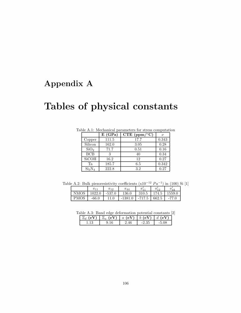
Appendix A
Tables of physical constants
Table A.1: Mechanical parameters for stress computationE (GPa) CTE (ppm/oC) ν
Copper 111.5 17.7 0.343Silicon 162.0 3.05 0.28SiO2 71.7 0.51 0.16BCB 3 40 0.34
SiCOH 16.2 12 0.27Ta 185.7 6.5 0.342
Si3N4 222.8 3.2 0.27
Table A.2: Bulk piezoresistivity coefficients (x10−12 Pa−1) in (100) Si [1]π11 π12 π44 π′
11 π′12 π′
44
NMOS 1022.0 -537.0 136.0 310.5 174.5 1559.0PMOS -66.0 11.0 -1381.0 -717.5 662.5 -77.0
Table A.3: Band edge deformation potential constants [2]Ξd (eV) Ξu (eV) a (eV) b (eV) d (eV)
1.13 9.16 2.46 -2.35 -5.08
106

107
Table A.4: FinFET piezoresitivity coeffs. in (100) Si [3]π′
11 (Pa−1) π′12 (Pa−1) π12 (Pa−1)
NMOS 452 × 10−12 256 × 10−12 −576× 10−12
PMOS −450× 10−12 238 × 10−12 101 × 10−12