Embed Size (px)
Citation preview

Page 1
Performance & Technology
Todd C. MowryCS 740
Sept 11, 2007Topics:
• Performance measures• Relating performance measures• Memory Technology
– SRAM, DRAM• Disk Technology• Recent Processor Trends
CS 740 F’072
Performance expressed as a time
Absolute time measures• difference between start and finish of an operation• synonyms: running time, elapsed time, response time, latency,
completion time, execution time• most straightforward performance measure
Relative (normalized) time measures• running time normalized to some reference time • (e.g. time/reference time)
Guiding principle: Choose performance measures that track running time.
CS 740 F’073
Performance expressed as a rate
Rates are performance measures expressed in units of work per unit time.
Examples:• millions of instructions / sec (MIPS)• millions of floating point instructions / sec (MFLOPS)• millions of bytes / sec (MBytes/sec)• millions of bits / sec (Mbits/sec)• images / sec• samples / sec• transactions / sec (TPS)
CS 740 F’074
Performance expressed as a rate(cont)
Key idea: Report rates that track execution time.
Example: Suppose we are measuring a program that convolves a stream of images from a video camera.
Bad performance measure: MFLOPS• number of floating point operations depends on the particular
convolution algorithm: n^2 matix-vector product vs nlogn fast Fourier transform. An FFT with a bad MFLOPS rate may run faster than a matrix-vector product with a good MFLOPS rate.
Good performance measure: images/sec• a program that runs faster will convolve more images per second.

Page 2
CS 740 F’075
Performance expressed as a rate(cont)
Fallacy: Peak rates track running time.
Example: the i860 is advertised as having a peak rate of 80 MFLOPS (40 MHz with 2 flops per cycle).
However, the measured performance of some compiled linear algebra kernels (icc -O2) tells a different story:
Kernel 1d fft sasum saxpy sdot sgemm sgemv spvmaMFLOPS 8.5 3.2 6.1 10.3 6.2 15.0 8.1%peak 11% 4% 7% 13% 8% 19% 10%
CS 740 F’076
Relating time to system measuresSuppose that for some program we have:
• T seconds running time (the ultimate performance measure)• C clock ticks, I instructions, P seconds/tick (performance
measures of interest to the system designer)
T secs = C ticks x P secs/tick= (I inst/I inst) x C ticks x P secs/tick
T secs = I inst x (C ticks/I inst) x P secs/tick
runningtime
instructioncount
avg clockticks perinstruction(CPI)
clock period
CS 740 F’077
Pipeline latency and throughput
video processing system(N input images)
In,...,I3, I2, I1
(N output images)
On,...,O3, O2, O1
Latency (L): time to process an individual image.
Throughput (R): images processed per unit time
One image can be processed by the system at any point in time
CS 740 F’078
Video system performance
L = 3 secs/image.
R = 1/L = 1/3 images/sec.
T = L + (N-1)1/R= 3N
time
1Stage 1
234567
1112223
1 out
2 out

Page 3
CS 740 F’079
Pipelining the video system
stage 1(buffer)
video pipeline
(L1,R1) (L3,R3)(L2,R2)
stage 3(display)
stage 2(CPU)
(N input images)
In,...,I3, I2, I1
(N output images)
On,...,O3, O2, O1
One image can be in each stage at any point in time.
Li = latency of stage iRi = throughput of stage i
L = L1 + L2 + L3R = min(R1, R2, R3)
CS 740 F’0710
Pipelined video system performance
time
1Suppose:
L1 = L2 = L3 = 1
Then:
L = 3 secs/image.
R = 1 image/sec.
T = L + (N-1)1/R= N + 2
Stage 1 Stage 2 Stage 3
234567
1234567
123456
12345
1 out2 out3 out4 out
CS 740 F’0711
Relating time to latency & throughput
In general:• T = L + (N-1)/R
The impact of latency and throughput on running time depends on N:• (N = 1) => (T = L)• (N >> 1) => (T = N/R)
To maximize throughput, we should try to maximize the minimum throughput over all stages (i.e., we strive for all stages to have equal throughput).
CS 740 F’0712
Amdahl’s law
You plan to visit a friend in Normandy France and must decide whether it is worth it to take the Concorde SST ($3,100) or a 747 ($1,021) from NY to Paris, assuming it will take 4 hours Pgh to NY and 4 hours Paris to Normandy.
time NY->Paris total trip time speedup over 747747 8.5 hours 16.5 hours 1SST 3.75 hours 11.75 hours 1.4
Taking the SST (which is 2.2 times faster) speeds up the overall trip by only a factor of 1.4!

Page 4
CS 740 F’0713
Amdahl’s law (cont)
T1 T2
Old program (unenhanced)T1 = time that can NOT
be enhanced.
T2 = time that can beenhanced.
T2’ = time after theenhancement.
Old time: T = T1 + T2
T1’ = T1 T2’ <= T2
New program (enhanced)
New time: T’ = T1’ + T2’
Speedup: Soverall = T / T’
CS 740 F’0714
Amdahl’s law (cont)Two key parameters:
Fenhanced = T2 / T (fraction of original time that can be improved)Senhanced = T2 / T2’ (speedup of enhanced part)
T’ = T1’ + T2’ = T1 + T2’ = T(1-Fenhanced) + T2’= T(1-Fenhanced) + (T2/Senhanced) [by def of Senhanced]= T(1-Fenhanced) + T(Fenhanced /Senhanced) [by def of Fenhanced]= T((1-Fenhanced) + Fenhanced/Senhanced)
Amdahl’s Law:Soverall = T / T’ = 1/((1-Fenhanced) + Fenhanced/Senhanced)
Key idea: Amdahl’s law quantifies the general notion of diminishing returns. It applies to any activity, not just computer programs.
CS 740 F’0715
Amdahl’s law (cont)
Trip example: Suppose that for the New York to Paris leg, we now consider the possibility of taking a rocket ship (15 minutes) or a handy rip in the fabric of space-time (0 minutes):
time NY->Paris total trip time speedup over 747747 8.5 hours 16.5 hours 1SST 3.75 hours 11.75 hours 1.4rocket 0.25 hours 8.25 hours 2.0rip 0.0 hours 8 hours 2.1
CS 740 F’0716
Amdahl’s law (cont)
Useful corollary to Amdahl’s law:• 1 <= Soverall <= 1 / (1 - Fenhanced)
Fenhanced Max Soverall Fenhanced Max Soverall
0.0 1 0.9375 16
0.5 2 0.96875 32
0.75 4 0.984375 64
0.875 8 0.9921875 128
Moral: It is hard to speed up a program.
Moral++ : It is easy to make premature optimizations.

Page 5
CS 740 F’0717
Computer System
DiskDisk
Memory-I/O busMemory-I/O bus
ProcessorProcessor
CacheCache
MemoryMemoryI/O
controllerI/O
controllerI/O
controllerI/O
controllerI/O
controllerI/O
controller
DisplayDisplay NetworkNetwork
Reg
CS 740 F’0718
Levels in Memory Hierarchy
CPUCPUregsregs
Cache
MemoryMemory diskdisk
size:speed:$/Mbyte:block size:
200 B3 ns
8 B
Register Cache Memory Disk Memory32 KB / 4MB6 ns$100/MB32 B
128 MB60 ns$1.50/MB8 KB
20 GB8 ms$0.05/MB
larger, slower, cheaper
8 B 32 B 8 KB
cache virtual memory
CS 740 F’0719
Scaling to 0.1µm
• Semiconductor Industry Association, 1992 Technology Workshop– Projected future technology based on past trends
1992 1995 1998 2001 2004 2007
Feature size: 0.5 0.35 0.25 0.18 0.12 0.10
– Industry is slightly ahead of projectionDRAM capacity: 16M 64M 256M 1G 4G 16G
– Doubles every 1.5 years– Prediction on track
Chip area (cm2): 2.5 4.0 6.0 8.0 10.0 12.5
– Way off! Chips staying small
CS 740 F’0720
Static RAM (SRAM)
Fast• ~4 nsec access time
Persistent • as long as power is supplied• no refresh required
Expensive • ~$100/MByte• 6 transistors/bit
Stable• High immunity to noise and environmental disturbances
Technology for caches

Page 6
CS 740 F’0721
Anatomy of an SRAM Cell
(6 transistors)
b b’bit line bit line
word line
Read:1. set bit lines high2. set word line high3. see which bit line goes low
Write:1. set bit lines to new data value
•b’ is set to the opposite of b2. raise word line to “high”⇒ sets cell to new state (may
involve flipping relative to old state)
0 1
Stable Configurations
1 0
Terminology:bit line: carries dataword line: used for addressing
CS 740 F’0722
SRAM Cell Principle
Inverter Amplifies• Negative gain• Slope < –1 in middle• Saturates at ends
Inverter Pair Amplifies• Positive gain• Slope > 1 in middle• Saturates at ends
VinV1
V2
V1V2
Vin
0 0.2 0.4 0.6 0.8 10
0.1
0.2
0.3
0.4
0.5
0.6
0.7
0.8
0.9
1
CS 740 F’0723
Bistable Element
Stability• Require Vin = V2• Stable at endpoints
– recover from pertubation• Metastable in middle
– Fall out when perturbed
Ball on Ramp Analogy
VinV1
V2
VinV2
Vin
0 0.2 0.4 0.6 0.8 10
0.1
0.2
0.3
0.4
0.5
0.6
0.7
0.8
0.9
1 Stable
Metastable
Stable 0 0.1 0.2 0.3 0.4 0.5 0.6 0.7 0.8 0.9 1
CS 740 F’0724
sense/writeamps
sense/writeamps
Example SRAM Configuration (16 x 8)
Addressdecoder
Addressdecoder
A0A1A2A3
b7’b7
d7
sense/writeamps
sense/writeamps
b1’b1
d1
sense/writeamps
sense/writeamps
b0’b0
d0Input/output lines
W0
W1
W15
memorycells
R/W
Page 7
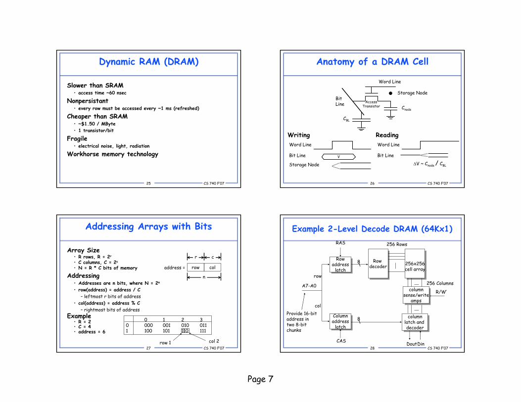
CS 740 F’0725
Dynamic RAM (DRAM)
Slower than SRAM • access time ~60 nsec
Nonpersistant• every row must be accessed every ~1 ms (refreshed)
Cheaper than SRAM • ~$1.50 / MByte• 1 transistor/bit
Fragile• electrical noise, light, radiation
Workhorse memory technology
CS 740 F’0726
Anatomy of a DRAM Cell
Word Line
BitLine
Storage Node
AccessTransistor Cnode
CBL
WritingWord Line
Bit Line
ReadingWord Line
Bit Line
ΔV ~ Cnode / CBL
V
Storage Node
CS 740 F’0727
rowaddress = col
0 1 2 30 000 001 010 0111 100 101 110 111
row 1 col 2
Addressing Arrays with Bits
Array Size• R rows, R = 2r
• C columns, C = 2c
• N = R * C bits of memory
Addressing• Addresses are n bits, where N = 2n
• row(address) = address / C – leftmost r bits of address
• col(address) = address % C – rightmost bits of address
Example• R = 2• C = 4• address = 6
r c
n
CS 740 F’0728
Example 2-Level Decode DRAM (64Kx1)
Rowaddress
latch
Rowaddress
latch
Columnaddress
latch
Columnaddress
latch
Row decoderRow
decoder 256x256cell array256x256cell array
columnlatch and decoder
columnlatch and decoder
A7-A0
\8
\8
R/W’
DoutDinCAS
RAS
row
col
256 Rows
256 Columnscolumn
sense/writeamps
columnsense/write
amps
Provide 16-bit address in two 8-bit chunks

Page 8
CS 740 F’0729
DRAM Operation
Row Address (~50ns)• Set Row address on address lines & strobe RAS• Entire row read & stored in column latches• Contents of row of memory cells destroyed
Column Address (~10ns)• Set Column address on address lines & strobe CAS• Access selected bit
– READ: transfer from selected column latch to Dout– WRITE: Set selected column latch to Din
Rewrite (~30ns)• Write back entire row
CS 740 F’0730
Observations About DRAMs
Timing• Access time (= 60ns) < cycle time (= 90ns)• Need to rewrite row
Must Refresh Periodically• Perform complete memory cycle for each row• Approximately once every 1ms• Sqrt(n) cycles• Handled in background by memory controller
Inefficient Way to Get a Single Bit• Effectively read entire row of Sqrt(n) bits
CS 740 F’0731
Enhanced Performance DRAMs
Rowaddress
latch
Rowaddress
latch
Columnaddress
latch
Columnaddress
latch
Row decoder
Row decoder 256x256
cell array
256x256cell array
sense/writeamps
sense/writeamps
columnlatch and decoder
columnlatch and decoder
A7-A0
\8
\8
R/W’
CAS
RAS
row
col
Entire row buffered here
row access time col access time cycle time page mode cycle time50ns 10ns 90ns 25ns
Conventional Access• Row + Col• RAS CAS RAS CAS ...
Page Mode• Row + Series of columns• RAS CAS CAS CAS ...• Gives successive bits
Other Acronyms• EDORAM
– “Extended data output”• SDRAM
– “Synchronous DRAM”
Typical Performance
CS 740 F’0732
Performance Enhanced for Video / Graphics Operations• Frame buffer to hold graphics image
Writing• Random access of bits• Also supports rectangle fill operations
– Set all bits in region to 0 or 1Reading
• Load entire row into shift register• Shift out at video rates
Performance Example• 1200 X 1800 pixels / frame• 24 bits / pixel• 60 frames / second• 2.8 GBits / second
256x256cell array256x256cell array
Shift RegisterShift Register
columnsense/write
amps
columnsense/write
amps
Video Stream Output
Video RAM

Page 9
CS 740 F’0733
DRAM Driving Forces
Capacity• 4X per generation
– Square array of cells• Typical scaling
– Lithography dimensions 0.7X» Areal density 2X
– Cell function packing 1.5X– Chip area 1.33X
• Scaling challenge– Typically Cnode / CBL = 0.1–0.2– Must keep Cnode high as shrink cell size
Retention Time• Typically 16–256 ms• Want higher for low-power applications
CS 740 F’0734
DRAM Storage Capacitor
d
Dielectric MaterialDielectric Constant ε
PlateArea A
C = εA/d
Planar Capacitor• Up to 1Mb• C decreases linearly with
feature size
Trench Capacitor• 4–256 Mb• Lining of hole in substrate
Stacked Cell• > 1Gb• On top of substrate• Use high ε dielectric
CS 740 F’0735
Trench Capacitor
Process• Etch deep hole in substrate
– Becomes reference plate• Grow oxide on walls
– Dielectric• Fill with polysilicon plug
– Tied to storage nodeStorage Plate
Reference Plate
SiO2 Dielectric
CS 740 F’0736
IBM DRAM Evolution
• IBM J. R&D, Jan/Mar ‘95• Evolution from 4 – 256 Mb• 256 Mb uses cell with area 0.6 µm2
4 Mb Cell Structure
Cell Layouts
4Mb
16Mb
64Mb
256Mb

Page 10
CS 740 F’0737
Mitsubishi Stacked Cell DRAM
• IEDM ‘95• Claim suitable for 1 – 4 Gb
Technology• 0.14 µm process
– Synchrotron X-ray source• 8 nm gate oxide• 0.29 µm2 cell
Storage Capacitor• Fabricated on top of everything else• Rubidium electrodes• High dielectric insulator
– 50X higher than SiO2– 25 nm thick
• Cell capacitance 25 femtofarads
Cross Section of 2 Cells
CS 740 F’0738
Mitsubishi DRAM Pictures
CS 740 F’0739
Magnetic Disks
The read/write head floats over the disk surface and moves back and forth on an arm from track to track.
Disk surface spins at3600–7200 RPM read/write head
armThe surface consistsof a set of concentricmagnetized rings called tracks
Each track is dividedinto sectors
CS 740 F’0740
Disk Capacity
Parameter 18GB Example• Number Platters 12• Surfaces / Platter 2• Number of tracks 6962• Number sectors / track 213• Bytes / sector 512
Total Bytes 18,221,948,928
Page 11
CS 740 F’0741
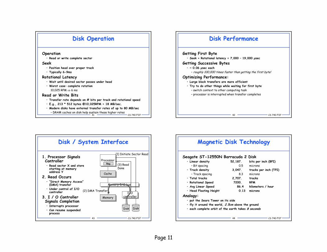
Disk Operation
Operation• Read or write complete sector
Seek• Position head over proper track• Typically 6-9ms
Rotational Latency• Wait until desired sector passes under head• Worst case: complete rotation
10,025 RPM ⇒ 6 ms
Read or Write Bits• Transfer rate depends on # bits per track and rotational speed • E.g., 213 * 512 bytes @10,025RPM = 18 MB/sec.• Modern disks have external transfer rates of up to 80 MB/sec
– DRAM caches on disk help sustain these higher ratesCS 740 F’0742
Disk Performance
Getting First Byte• Seek + Rotational latency = 7,000 – 19,000 µsec
Getting Successive Bytes• ~ 0.06 µsec each
– roughly 100,000 times faster than getting the first byte!Optimizing Performance:
• Large block transfers are more efficient• Try to do other things while waiting for first byte
– switch context to other computing task– processor is interrupted when transfer completes
CS 740 F’0743
Disk / System Interface
1. Processor Signals Controller• Read sector X and store
starting at memory address Y
2. Read Occurs• “Direct Memory Access”
(DMA) transfer• Under control of I/O
controller
3. I / O Controller Signals Completion• Interrupts processor• Can resume suspended
process DiskDisk
Memory-I/O busMemory-I/O bus
ProcessorProcessor
CacheCache
MemoryMemoryI/O
controllerI/O
controller
Reg
(2) DMA Transfer
(1) Initiate Sector Read
(3) Read Done
CS 740 F’0744
Magnetic Disk Technology
Seagate ST-12550N Barracuda 2 Disk• Linear density 52,187. bits per inch (BPI)
– Bit spacing 0.5 microns• Track density 3,047. tracks per inch (TPI)
– Track spacing 8.3 microns• Total tracks 2,707. tracks• Rotational Speed 7200. RPM• Avg Linear Speed 86.4 kilometers / hour• Head Floating Height 0.13 microns
Analogy:• put the Sears Tower on its side• fly it around the world, 2.5cm above the ground• each complete orbit of the earth takes 8 seconds

Page 12
CS 740 F’0745
Storage Trends
metric 1980 1985 1990 1995 2000 2005 2005:1980
$/MB 8,000 880 100 30 1 0.20 40,000access (ns) 375 200 100 70 60 50 8typical size(MB) 0.064 0.256 4 16 64 1,000 15,000
DRAM
metric 1980 1985 1990 1995 2000 2005 2005:1980
$/MB 19,200 2,900 320 256 100 75 256access (ns) 300 150 35 15 12 10 30
SRAM
metric 1980 1985 1990 1995 2000 2005 2005:1980
$/MB 500 100 8 0.30 0.05 0.001 10,000access (ms) 87 75 28 10 8 4 22typical size(MB) 1 10 160 1,000 9,000 400,000400,000
Disk
CS 740 F’0746
CPU Clock Rates
1980 1985 1990 1995 2000 2005 2005:1980
processor 8080 286 386 Pentium P-III P-4
clock rate(MHz) 1 6 20 150 750 3,000 3,000cycle time(ns) 1,000 166 50 6 1.3 0.3 3,333
CS 740 F’0747
The CPU-Memory Gap
01
10100
1,00010,000
100,0001,000,000
10,000,000100,000,000
1980 1985 1990 1995 2000 2005
Year
ns Disk seek timeDRAM access timeSRAM access timeCPU cycle time
The gap widens between DRAM, disk, and CPU speeds. The gap widens between DRAM, disk, and CPU speeds.
CS 740 F’0748
Memory Technology Summary
Cost and Density Improving at Enormous RatesSpeed Lagging Processor PerformanceMemory Hierarchies Help Narrow the Gap:
• Small fast SRAMS (cache) at upper levels• Large slow DRAMS (main memory) at lower levels• Incredibly large & slow disks to back it all up
Locality of Reference Makes It All Work• Keep most frequently accessed data in fastest memory
Page 13
CS 740 F’0749
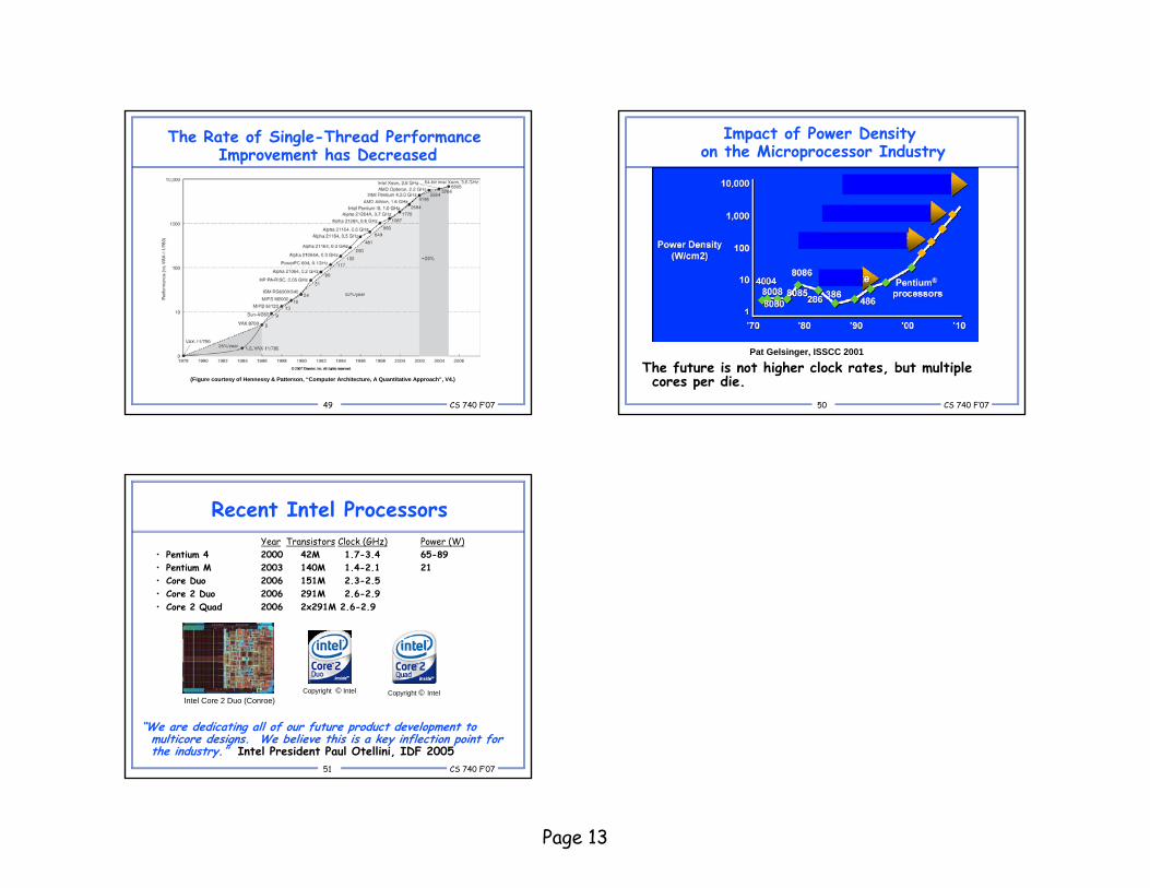
The Rate of Single-Thread Performance Improvement has Decreased
(Figure courtesy of Hennessy & Patterson, “Computer Architecture, A Quantitative Approach”, V4.)
CS 740 F’0750
Impact of Power Density on the Microprocessor Industry
The future is not higher clock rates, but multiple cores per die.
Pat Gelsinger, ISSCC 2001
CS 740 F’0751
Recent Intel ProcessorsYear Transistors Clock (GHz) Power (W)
• Pentium 4 2000 42M 1.7-3.4 65-89• Pentium M 2003 140M 1.4-2.1 21 • Core Duo 2006 151M 2.3-2.5• Core 2 Duo 2006 291M 2.6-2.9• Core 2 Quad 2006 2x291M 2.6-2.9
“We are dedicating all of our future product development to multicore designs. We believe this is a key inflection point for the industry.” Intel President Paul Otellini, IDF 2005
Intel Core 2 Duo (Conroe)Copyright © Intel Copyright © Intel