Embed Size (px)
Citation preview
Performance of the IQPro DDS VFO and Evaluation of Wideband Opamps Gary W. Johnson, WB9JPS Rev. 1, August 5, 2006
Abstract Direct digital synthesis (DDS) ICs are very attractive in amateur radio applications, particularly in test equipment and VFOs. One DDS-VFO kit, the IQPro, was recently developed by Craig Johnson, AA0ZZ. Based on the Analog Devices AD9854, it provides quadrature outputs and has several options for RF output drivers including transformer coupling and/or a transistor amplifier. In the first part of this report, output spectra for the transformer option (+3 dBm output) are shown to meet the manufacturer’s specifications, and phase noise is very low. The transistor amplifier (at +13 dBm output) shows some problematic spurious response at higher frequencies. Experiments and suggestions for improvement are discussed. In the second part, several state-of-the-art wideband operational amplifiers are evaluated. For outputs up to +13 dBm, the LMH6703 offers low distortion and exceptional bandwidth. For greater output, up to +20 dBm, the THS6012 is usable. All of these devices are affordable and may be of great utility, especially to the hobbyist. Revision History May 20, 2006. Original release. August 5, 2006. Update per comments from W7ZOI. Expanded phase noise section.
Introduction Direct digital synthesis (DDS) ICs are very attractive in amateur radio applications, particularly in test equipment and VFOs. One DDS-VFO kit, the IQPro, was recently developed by Craig Johnson, AA0ZZ1. Based on the Analog Devices AD9854, it provides quadrature outputs up to 30 MHz and has several options for RF output drivers including transformer coupling and/or a transistor amplifier. Two PIC microcontrollers support an LCD display and a keypad. Source code is supplied for those who wish to modify it. The manual is substantial and very thorough. Anyone with reasonable kit building experience will have no problem with assembly. I think it’s a great value as a modern VFO, and a wonderful learning tool as well. After assembling mine, I wanted to check its performance and see how compatible it would be with an image-canceling direct-conversion receiver. A good spectrum analyzer is the key to such measurements, so I finally spent a pile of cash on a classic laboratory
1 The IQPro: A High-Performance Quadrature DDS VFO, QEX, May-June, 2006. Also see Craig’s web page at http://home.comcast.net/~aa0zz/index.html. Kits are available from Bill Kelsey, N8ET, at http://www.kangaus.com.
2
instrument, an HP8568B. With a few test accessories such as filters and attenuators, and some experience, reliable results are now at hand. Boosting the output of a DDS is required to drive high-level mixers. I was especially interested in seeing how hard it would be to reach +17 dBm since that would possibly lead to better receiver dynamic range. Because of my experience with high-performance analog systems in instrumentation, I decided to organize a “drag race” between state-of-the-art wideband opamps. The second part of this report contains an extensive characterization of several such devices. My intent with this report is to give the ham community some data on the IQPro and wideband amplifiers. Maybe I can pass along some advice as well. Consider this report a work in progress. I may update it with additional data, and I look forward to comments.
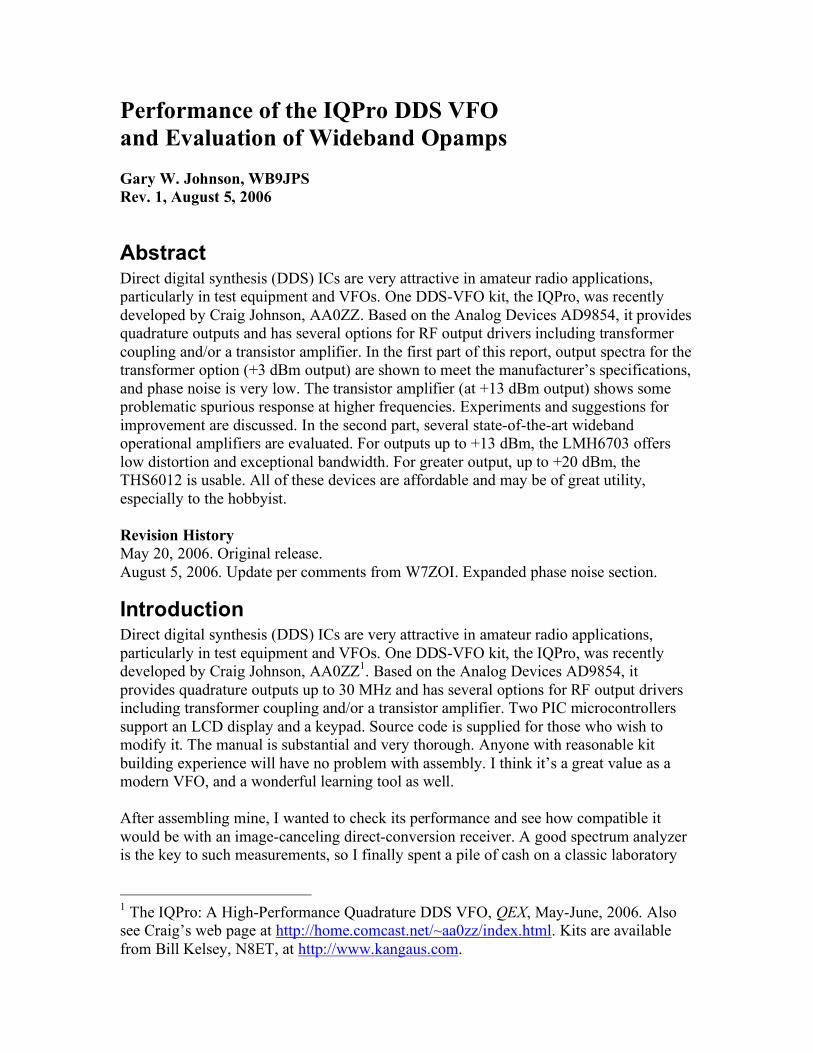
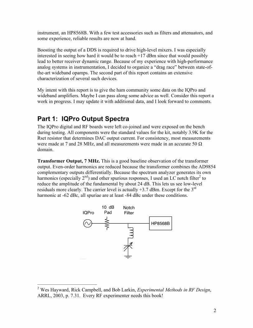
Part 1: IQPro Output Spectra The IQPro digital and RF boards were left co-joined and were exposed on the bench during testing. All components were the standard values for the kit, notably 3.9K for the Rset resistor that determines DAC output current. For consistency, most measurements were made at 7 and 28 MHz, and all measurements were made in an accurate 50 Ω domain. Transformer Output, 7 MHz. This is a good baseline observation of the transformer output. Even-order harmonics are reduced because the transformer combines the AD9854 complementary outputs differentially. Because the spectrum analyzer generates its own harmonics (especially 2nd) and other spurious responses, I used an LC notch filter2 to reduce the amplitude of the fundamental by about 24 dB. This lets us see low-level residuals more clearly. The carrier level is actually +3.7 dBm. Except for the 3rd harmonic at -62 dBc, all spuriae are at least -84 dBc under these conditions.
2 Wes Hayward, Rick Campbell, and Bob Larkin, Experimental Methods in RF Design, ARRL, 2003, p. 7.31. Every RF experimenter needs this book!
3
-90
-80
-70
-60
-50
-40
-30
-20
dBm
252015105
MHz
Second harmonic-79.5 dBc
Fundamental attenuated approx. 24 dB by notch filter
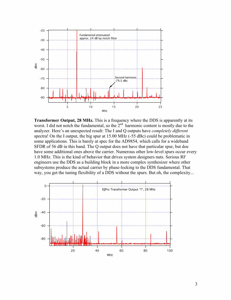
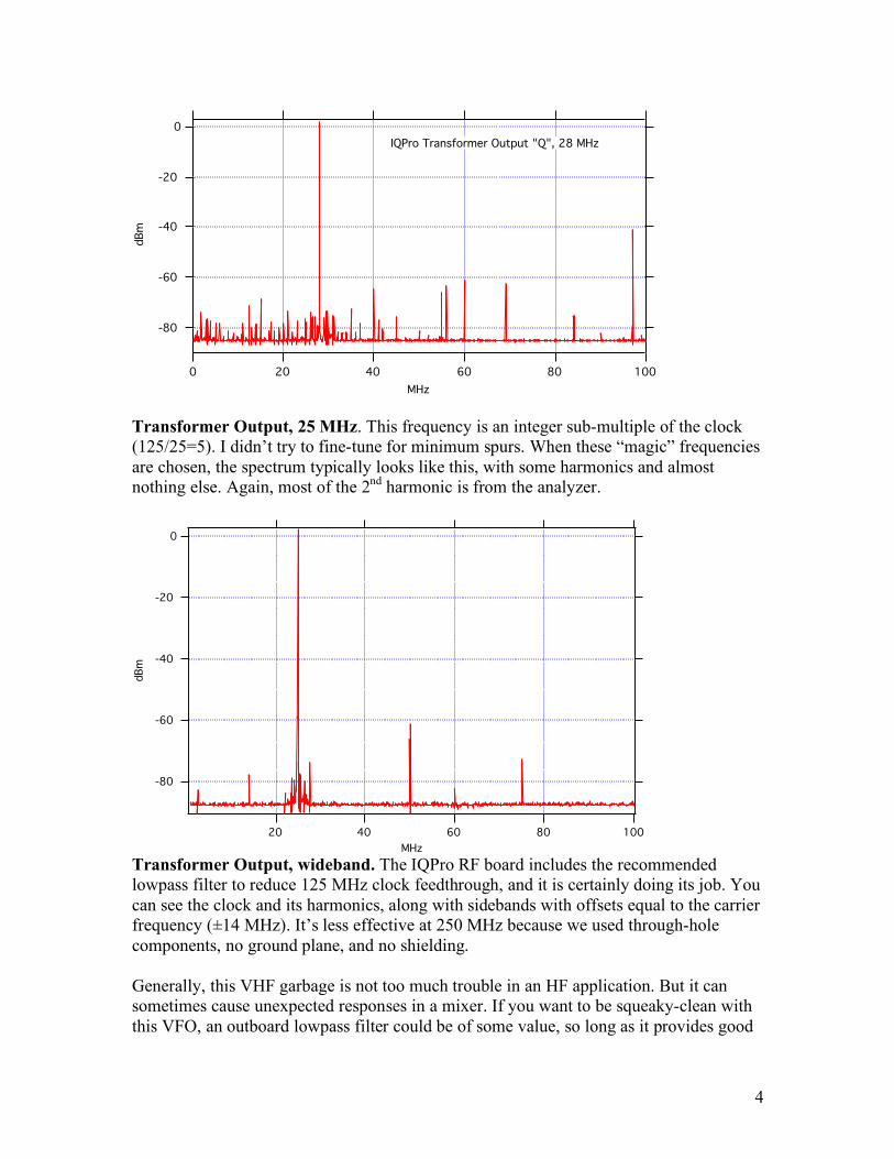
Transformer Output, 28 MHz. This is a frequency where the DDS is apparently at its worst. I did not notch the fundamental, so the 2nd harmonic content is mostly due to the analyzer. Here’s an unexpected result: The I and Q outputs have completely different spectra! On the I output, the big spur at 15.00 MHz (-55 dBc) could be problematic in some applications. This is barely at spec for the AD9854, which calls for a wideband SFDR of 56 dB in this band. The Q output does not have that particular spur, but doe have some additional ones above the carrier. Numerous other low-level spurs occur every 1.0 MHz. This is the kind of behavior that drives system designers nuts. Serious RF engineers use the DDS as a building block in a more complex synthesizer where other subsystems produce the actual carrier by phase-locking to the DDS fundamental. That way, you get the tuning flexibility of a DDS without the spurs. But oh, the complexity...
-80
-60
-40
-20
0
dBm
10080604020
MHz
IQPro Transformer Output "I", 28 MHz
4
-80
-60
-40
-20
0dBm
100806040200
MHz
IQPro Transformer Output "Q", 28 MHz
Transformer Output, 25 MHz. This frequency is an integer sub-multiple of the clock (125/25=5). I didn’t try to fine-tune for minimum spurs. When these “magic” frequencies are chosen, the spectrum typically looks like this, with some harmonics and almost nothing else. Again, most of the 2nd harmonic is from the analyzer.
-80
-60
-40
-20
0
dBm
10080604020
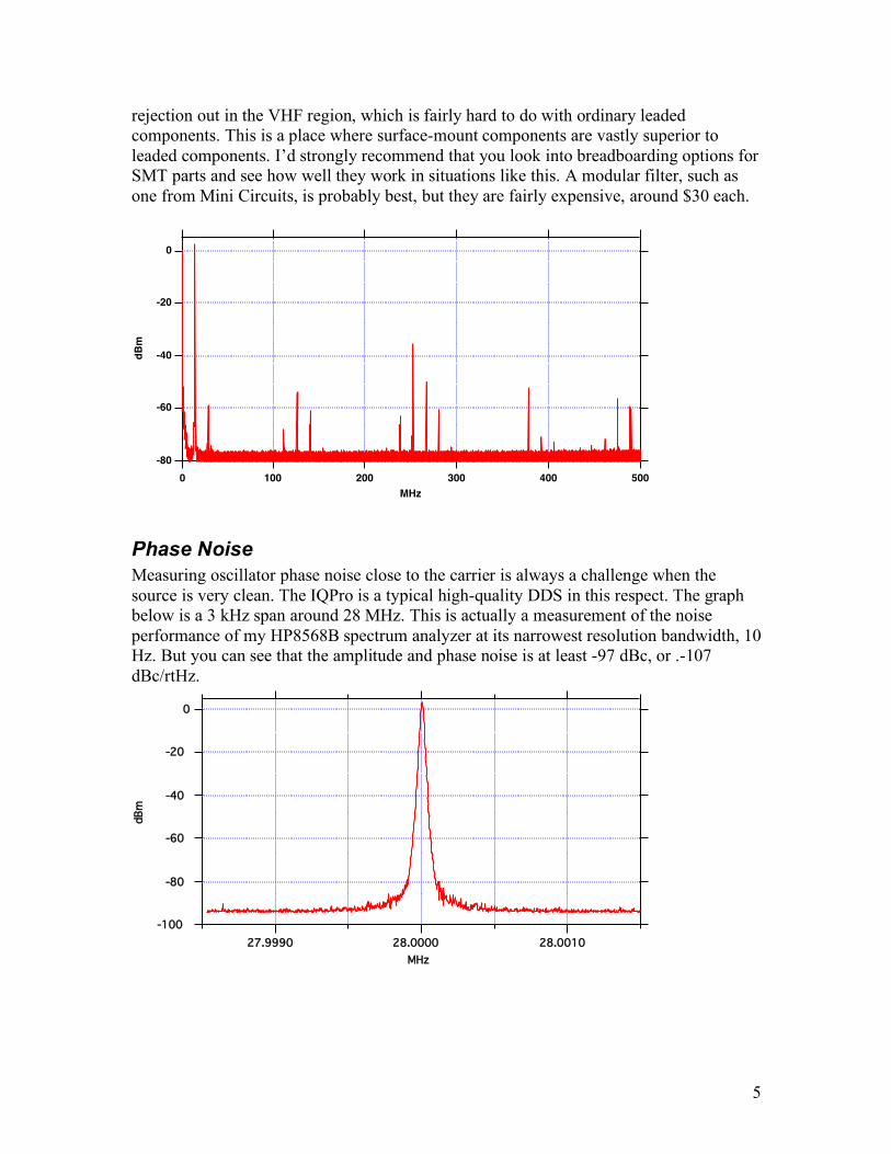
MHz Transformer Output, wideband. The IQPro RF board includes the recommended lowpass filter to reduce 125 MHz clock feedthrough, and it is certainly doing its job. You can see the clock and its harmonics, along with sidebands with offsets equal to the carrier frequency (±14 MHz). It’s less effective at 250 MHz because we used through-hole components, no ground plane, and no shielding. Generally, this VHF garbage is not too much trouble in an HF application. But it can sometimes cause unexpected responses in a mixer. If you want to be squeaky-clean with this VFO, an outboard lowpass filter could be of some value, so long as it provides good
5
rejection out in the VHF region, which is fairly hard to do with ordinary leaded components. This is a place where surface-mount components are vastly superior to leaded components. I’d strongly recommend that you look into breadboarding options for SMT parts and see how well they work in situations like this. A modular filter, such as one from Mini Circuits, is probably best, but they are fairly expensive, around $30 each.
-80
-60
-40
-20
0
dBm
5004003002001000
MHz
Phase Noise Measuring oscillator phase noise close to the carrier is always a challenge when the source is very clean. The IQPro is a typical high-quality DDS in this respect. The graph below is a 3 kHz span around 28 MHz. This is actually a measurement of the noise performance of my HP8568B spectrum analyzer at its narrowest resolution bandwidth, 10 Hz. But you can see that the amplitude and phase noise is at least -97 dBc, or .-107 dBc/rtHz.
-100
-80
-60
-40
-20
0
dBm
28.001028.000027.9990
MHz
6
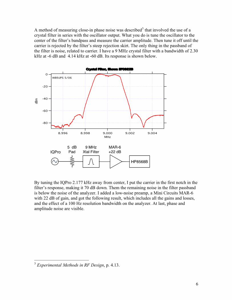
A method of measuring close-in phase noise was described3 that involved the use of a crystal filter in series with the oscillator output. What you do is tune the oscillator to the center of the filter’s bandpass and measure the carrier amplitude. Then tune it off until the carrier is rejected by the filter’s steep rejection skirt. The only thing in the passband of the filter is noise, related to carrier. I have a 9 MHz crystal filter with a bandwidth of 2.30 kHz at -6 dB and 4.14 kHz at -60 dB. Its response is shown below.
-80
-60
-40
-20
0
dBm
9.0049.0029.0008.9988.996
MHz
Crystal Filter, Showa SF0922B
WB9JPS 5/06
By tuning the IQPro 2.177 kHz away from center, I put the carrier in the first notch in the filter’s response, making it 70 dB down. Them the remaining noise in the filter passband is below the noise of the analyzer. I added a low-noise preamp, a Mini Circuits MAR-6 with 22 dB of gain, and got the following result, which includes all the gains and losses, and the effect of a 100 Hz resolution bandwidth on the analyzer. At last, phase and amplitude noise are visible.
3 Experimental Methods in RF Design, p. 4.13.
7
-160
-150
-140
-130
-120
-110
-100
dBc/rt
Hz
9.0049.0029.0008.9988.996
MHz
Tune IQPro
Noise
FilterPassband
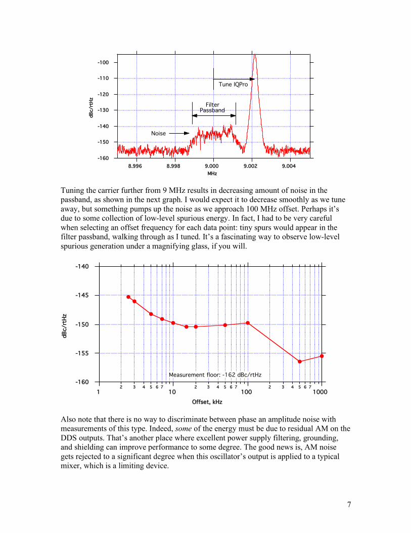
Tuning the carrier further from 9 MHz results in decreasing amount of noise in the passband, as shown in the next graph. I would expect it to decrease smoothly as we tune away, but something pumps up the noise as we approach 100 MHz offset. Perhaps it’s due to some collection of low-level spurious energy. In fact, I had to be very careful when selecting an offset frequency for each data point: tiny spurs would appear in the filter passband, walking through as I tuned. It’s a fascinating way to observe low-level spurious generation under a magnifying glass, if you will.
-160
-155
-150
-145
-140
dBc/rt
Hz
12 3 4 5 6 7
102 3 4 5 6 7
1002 3 4 5 6 7
1000
Offset, kHz
Measurement floor: -162 dBc/rtHz
Also note that there is no way to discriminate between phase an amplitude noise with measurements of this type. Indeed, some of the energy must be due to residual AM on the DDS outputs. That’s another place where excellent power supply filtering, grounding, and shielding can improve performance to some degree. The good news is, AM noise gets rejected to a significant degree when this oscillator’s output is applied to a typical mixer, which is a limiting device.
8
That’s the best I can do with my available equipment, but at least it proves this is indeed a quiet oscillator with regards to wideband phase noise.
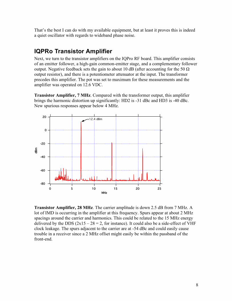
IQPRo Transistor Amplifier Next, we turn to the transistor amplifiers on the IQPro RF board. This amplifier consists of an emitter follower, a high-gain common-emitter stage, and a complementary follower output. Negative feedback sets the gain to about 10 dB (after accounting for the 50 Ω output resistor), and there is a potentiometer attenuator at the input. The transformer precedes this amplifier. The pot was set to maximum for these measurements and the amplifier was operated on 12.6 VDC. Transistor Amplifier, 7 MHz. Compared with the transformer output, this amplifier brings the harmonic distortion up significantly: HD2 is -31 dBc and HD3 is -40 dBc. New spurious responses appear below 4 MHz.
-80
-60
-40
-20
0
20
dBm
2520151050
MHz
+12.4 dBm
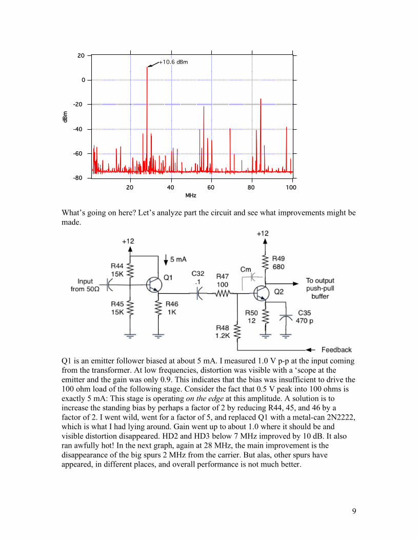
Transistor Amplifier, 28 MHz. The carrier amplitude is down 2.5 dB from 7 MHz. A lot of IMD is occurring in the amplifier at this frequency. Spurs appear at about 2 MHz spacings around the carrier and harmonics. This could be related to the 15 MHz energy delivered by the DDS (2x15 – 28 = 2, for instance). It could also be a side-effect of VHF clock leakage. The spurs adjacent to the carrier are at -54 dBc and could easily cause trouble in a receiver since a 2 MHz offset might easily be within the passband of the front-end.
9
-80
-60
-40
-20
0
20
dBm
10080604020
MHz
+10.6 dBm
What’s going on here? Let’s analyze part the circuit and see what improvements might be made.
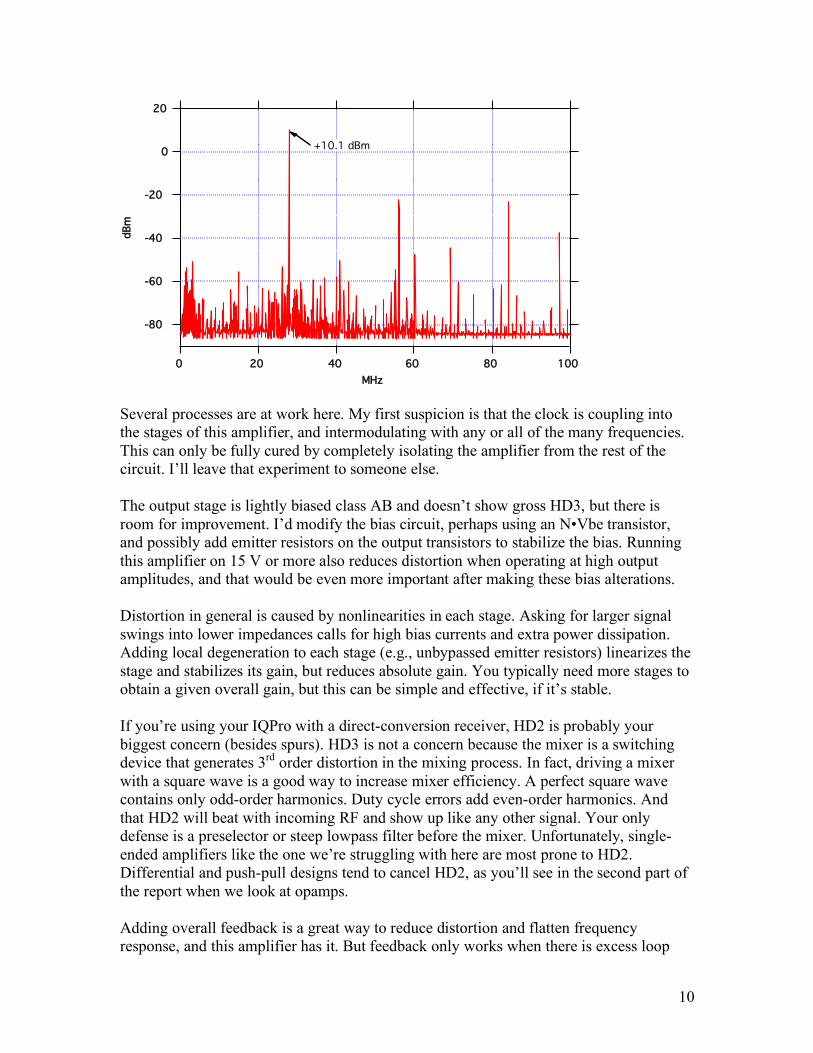
Q1 is an emitter follower biased at about 5 mA. I measured 1.0 V p-p at the input coming from the transformer. At low frequencies, distortion was visible with a ‘scope at the emitter and the gain was only 0.9. This indicates that the bias was insufficient to drive the 100 ohm load of the following stage. Consider the fact that 0.5 V peak into 100 ohms is exactly 5 mA: This stage is operating on the edge at this amplitude. A solution is to increase the standing bias by perhaps a factor of 2 by reducing R44, 45, and 46 by a factor of 2. I went wild, went for a factor of 5, and replaced Q1 with a metal-can 2N2222, which is what I had lying around. Gain went up to about 1.0 where it should be and visible distortion disappeared. HD2 and HD3 below 7 MHz improved by 10 dB. It also ran awfully hot! In the next graph, again at 28 MHz, the main improvement is the disappearance of the big spurs 2 MHz from the carrier. But alas, other spurs have appeared, in different places, and overall performance is not much better.
10
-80
-60
-40
-20
0
20
dBm
100806040200
MHz
+10.1 dBm
Several processes are at work here. My first suspicion is that the clock is coupling into the stages of this amplifier, and intermodulating with any or all of the many frequencies. This can only be fully cured by completely isolating the amplifier from the rest of the circuit. I’ll leave that experiment to someone else. The output stage is lightly biased class AB and doesn’t show gross HD3, but there is room for improvement. I’d modify the bias circuit, perhaps using an N•Vbe transistor, and possibly add emitter resistors on the output transistors to stabilize the bias. Running this amplifier on 15 V or more also reduces distortion when operating at high output amplitudes, and that would be even more important after making these bias alterations. Distortion in general is caused by nonlinearities in each stage. Asking for larger signal swings into lower impedances calls for high bias currents and extra power dissipation. Adding local degeneration to each stage (e.g., unbypassed emitter resistors) linearizes the stage and stabilizes its gain, but reduces absolute gain. You typically need more stages to obtain a given overall gain, but this can be simple and effective, if it’s stable. If you’re using your IQPro with a direct-conversion receiver, HD2 is probably your biggest concern (besides spurs). HD3 is not a concern because the mixer is a switching device that generates 3rd order distortion in the mixing process. In fact, driving a mixer with a square wave is a good way to increase mixer efficiency. A perfect square wave contains only odd-order harmonics. Duty cycle errors add even-order harmonics. And that HD2 will beat with incoming RF and show up like any other signal. Your only defense is a preselector or steep lowpass filter before the mixer. Unfortunately, single-ended amplifiers like the one we’re struggling with here are most prone to HD2. Differential and push-pull designs tend to cancel HD2, as you’ll see in the second part of the report when we look at opamps. Adding overall feedback is a great way to reduce distortion and flatten frequency response, and this amplifier has it. But feedback only works when there is excess loop
11
gain to begin with, and that peters out at high frequencies. Consider poor Q2. It is solely responsible for all the voltage gain in this amplifier. At 28 MHz and with a gain of 10, the overall amplifier has a GBW of 280 MHz. A 2N3904 has an ft of 300 MHz, maybe more. That means feedback is doing little or nothing for us at the top end of the HF bands. Things get worse when you consider Miller capacitance (Cm, from collector to emitter), which reduces bandwidth even further. Solutions include using real UHF RF transistors or FETs, and topologies like cascode. Remember, this is a WIDEBAND amplifier. That’s why superhet designs are so forgiving: all their stages are narrow-bandwidth and are easy to optimize. But here, we demand not only flat amplitude response over 1.5 decades of bandwidth, but also consistent phase response to avoid quadrature errors where even a fraction of one degree difference may be significant. All in all, these are demanding requirements and none of the really effective solutions are simple. Want to see some good designs? Study at the vertical amplifiers used in oscilloscopes4.
4 Many classic manuals are available online from the Boatanchor arhive, http://bama.sbc.edu/ I use the more-reliable mirror site, ftp://bama.edebris.com/bama. For example, check out the Tek 7A29 1-GHz vertical amplifier. Those engineers were incredible. Barrie Gilbert was a key designer on the Tek 7000 series, inventing his famed Glibert Cell analog multiplier during that era.
12
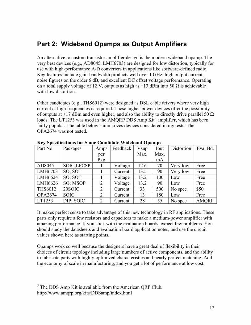
Part 2: Wideband Opamps as Output Amplifiers An alternative to custom transistor amplifier design is the modern wideband opamp. The very best devices (e.g., AD8045, LMH6703) are designed for low distortion, typically for use with high-performance A/D converters in applications like software-defined radio. Key features include gain-bandwidth products well over 1 GHz, high output current, noise figures on the order 6 dB, and excellent DC offset voltage performance. Operating on a total supply voltage of 12 V, outputs as high as +13 dBm into 50 Ω is achievable with low distortion. Other candidates (e.g., THS6012) were designed as DSL cable drivers where very high current at high frequencies is required. These higher-power devices offer the possibility of outputs at +17 dBm and even higher, and also the ability to directly drive parallel 50 Ω loads. The LT1253 was used in the AMQRP DDS Amp Kit5 amplifier, which has been fairly popular. The table below summarizes devices considered in my tests. The OPA2674 was not tested. Key Specifications for Some Candidate Wideband Opamps Part No. Packages Amps
per Pkg
Feedback Vsup Max.
Iout Max. mA
Distortion Eval Bd.
AD8045 SOIC;LFCSP 1 Voltage 12.6 70 Very low Free LMH6703 SO; SOT 1 Current 13.5 90 Very low Free LMH6624 SO; SOT 1 Voltage 13.2 100 Low Free LMH6626 SO; MSOP 2 Voltage 13.2 90 Low Free THS6012 20SOIC 2 Current 33 500 No spec $50 OPA2674 SOIC 2 Current 13 180 Low Free LT1253 DIP; SOIC 2 Current 28 55 No spec AMQRP It makes perfect sense to take advantage of this new technology in RF applications. These parts only require a few resistors and capacitors to make a medium-power amplifier with amazing performance. If you stick with the evaluation boards, expect few problems. You should study the datasheets and evaluation board application notes, and use the circuit values shown here as starting points. Opamps work so well because the designers have a great deal of flexibility in their choices of circuit topology including large numbers of active components, and the ability to fabricate parts with highly-optimized characteristics and nearly perfect matching. Add the economy of scale in manufacturing, and you get a lot of performance at low cost.
5 The DDS Amp Kit is available from the American QRP Club. http://www.amqrp.org/kits/DDSamp/index.html
13
Test Procedures Test equipment consisted of an HP8568B spectrum analyzer with HP8444A tracking generator, the IQPro transformer output as a CW RF source, a homebrew RF power meter6 and several attenuators. Data was acquired on my trusty old blue and white Macintosh G3 via GPIB, running LabVIEW for acquisition and control, and analysis and plotting in Wavemetrics’ Igor Pro. Distortion and spuriae were observed directly with the spectrum analyzer; all distortion products were checked to be sure that they were not induced by the analyzer. You should consult the first part of this report for input spectra as produced by the IQPro on its transformer output. The 28 MHz case is especially interesting and challenging for any amplifier because intermodulation distortion is more likely with this complex input signal. Since my application focused on DDS post-amplifiers to drive high-level mixers, all devices were operated near maximum output short of gross distortion. This was typically +10 to 13 dBm at 7 MHz, and sometimes a dB or two lower at 28 MHz, depending upon frequency response. Note that you can always obtain much lower distortion by operating at lower output power. Frequency response was measured with the tracking generator, typically adjusted for +13 dBm at the output the device under test (DUT) at a few MHz. Reference scans were taken to compensate for generator flatness. Frequency response and harmonic distortion charts for all devices appear at the end of this report. Evaluation boards from each IC’s manufacturer were used except for the AMQRP board. ICs and eval boards are available as samples, and you can also get many of the eval boards from DigiKey. Sources and part numbers are noted in each section. All amplifiers were configured non-inverting. This simplifies input matching but sometimes increases distortion due to the fact that there is a large, continuous common-mode signal. A 50 Ω output resistor provides a conjugate match. Connectors were mostly SMA. Power supplies were complementary (except for the AMQRP). This is highly recommended for all high-performance opamp applications because it reduces common-mode coupling problems and eliminates a source for noise at the inputs (from the ½ supply source). Most of the amplifiers were rated for 13 V maximum total supply voltage, and were run at ±6.0 V. Components were all surface-mount. Resistors were 0603 1% metal film and bypass capacitors were 0.1 µF 0603 ceramics. Only the AD8045 board required 0603 parts; all other boards had pads for 0805 or larger. I use a simple head-mounted 2X magnifier, and a 50 W halogen lamp at my bench, and that seems more than adequate even for the 0603 parts. I use a high-quality pair of tweezers designed for SMT placement, 15-mil solder, liquid soldering flux, and the finest tip that Weller makes for the WTCPN soldering station.
6 Wes Hayward, and Bob Larkin, “Simple RF-Power Measurement”, QST, June, 2001.
14
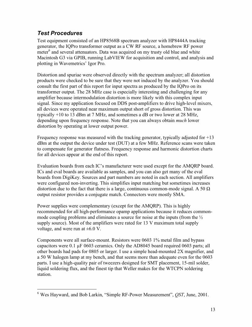
AD8045 The Analog Devices AD8045 is a voltage-feedback device designed for ultralow distortion and noise. It has an unusual package with an extra inverting input terminal to optimize frequency response and distortion. From the datasheet, we expect a bandwidth of over 40 MHz with a gain of 10 and reasonable component values. Free samples are available from Analog.com. I used an AD8045ARD SOIC with exposed paddle. Free eval board: EVAL-ADOPAMP-1R-E. ICs are $2.09 at DigiKey. Note: The eval board requires 0603 components.
The graph shows the spectrum at 28 MHz with an input of +3 dBm and an output of +13.7. Except for some added harmonic distortion, this is a perfectly amplified version of the input. Frequency response is down 1.1 dB at 28 MHz. This is a fine amplifier for applications up to +13 dBm output. At low levels, distortion essentially vanishes.
-80
-60
-40
-20
0
20
dBm
100806040200
MHz
+13.5 dBm
MHz Input dBm Fund dBm HD2 dBc HD3 dBc 7 2.6 13.8 -54.6 -61.9 28 3.0 13.7 -46.1 -61.1 28 0.4 10.5 -48.6 -68.7
15
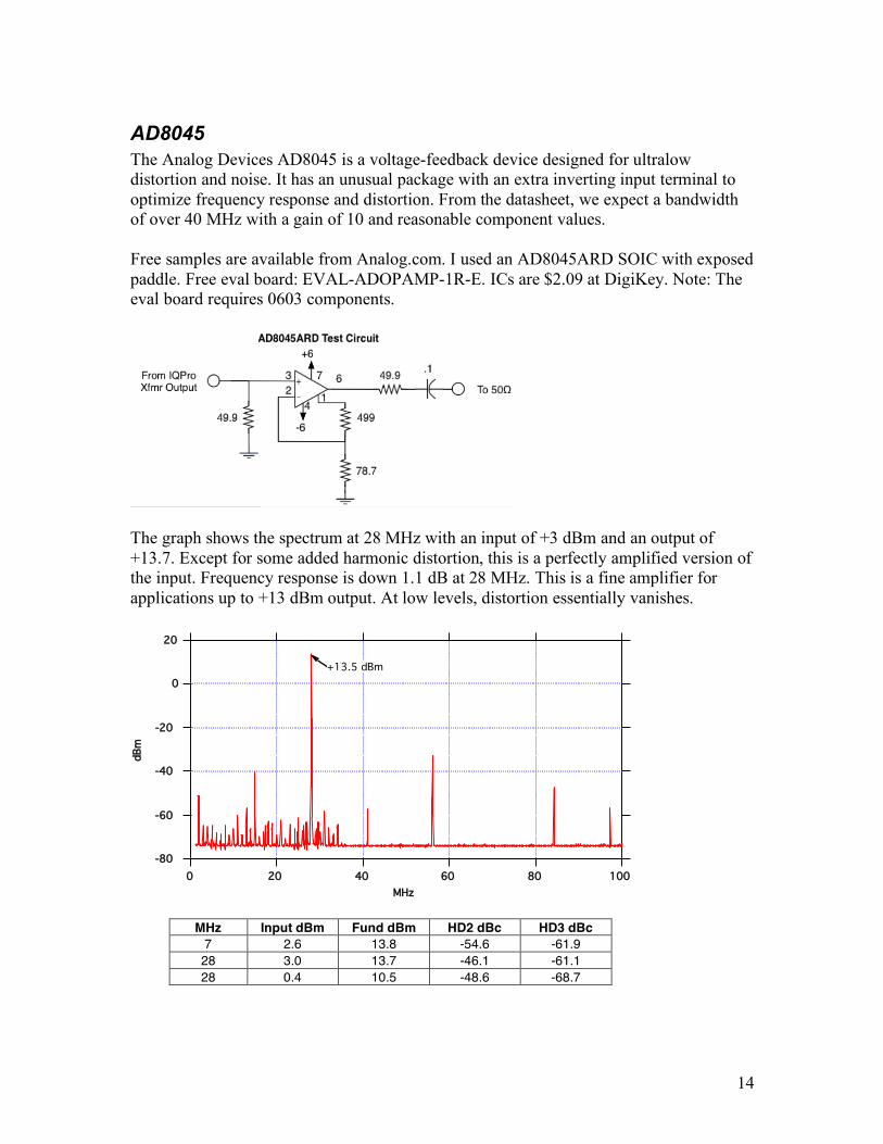
THS6012 The mighty Texas Instruments THS6012 current-feedback opamp was designed as a DSL differential cable driver and has a 400 mA output current capability on each of two channels. This allows it to operate in its linear range out to 140 MHz into 25 Ω loads. Thus, you could well use it as a lossless splitter, driving two back-terminated 50 Ω loads in parallel. It runs on ±15 V and has a special thermal management package that uses the PC board as a heatsink. In this test, my intent was to use it as a driver for +17 dBm mixers, so the gain was set to 17 dB. This would allow the IQPro to drive a power splitter with one output for a transmitter, the other for the receiver, giving a 0 dBm signal to each. Free samples available from TI; I used the THS6012CDWP. Fully-loaded eval boards cost $63 from DigiKey (p/n 296-10061-ND), or $49 from the online TI store. (You will need to change some resistor values to adjust gain.) ICs cost $7.12 from Digi-Key. I also made a heroic attempt at breadboarding this device with leaded components. It worked nearly as well as the official eval board except for poorer frequency response due to stray L and C, no doubt. I strongly recommend using a proper double-sided board for this device. Too bad the eval board is not available unloaded; it would be much more affordable.
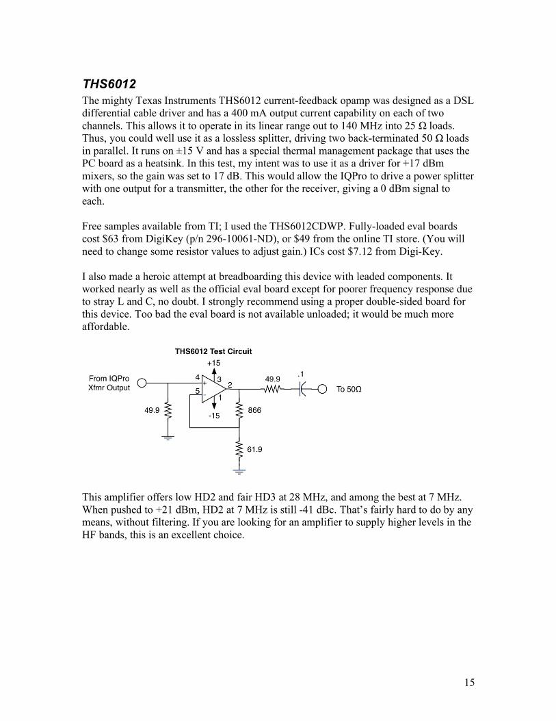
This amplifier offers low HD2 and fair HD3 at 28 MHz, and among the best at 7 MHz. When pushed to +21 dBm, HD2 at 7 MHz is still -41 dBc. That’s fairly hard to do by any means, without filtering. If you are looking for an amplifier to supply higher levels in the HF bands, this is an excellent choice.
16
-80
-60
-40
-20
0
20
dBm
100806040200
MHz
+17 dBm
MHz Input dBm Fund dBm HD2 dBc HD3 dBc 7 -4 13.6 -44.7 -61.1 7 0.7 17 -42.8 -56.1 7 3.7 21.3 -41.3 -52.9 28 -4 13.1 -47.7 -40.1 28 0.4 16.9 -53.7 -36.1 28 3.5 17.9 -46.9 -30.5
17
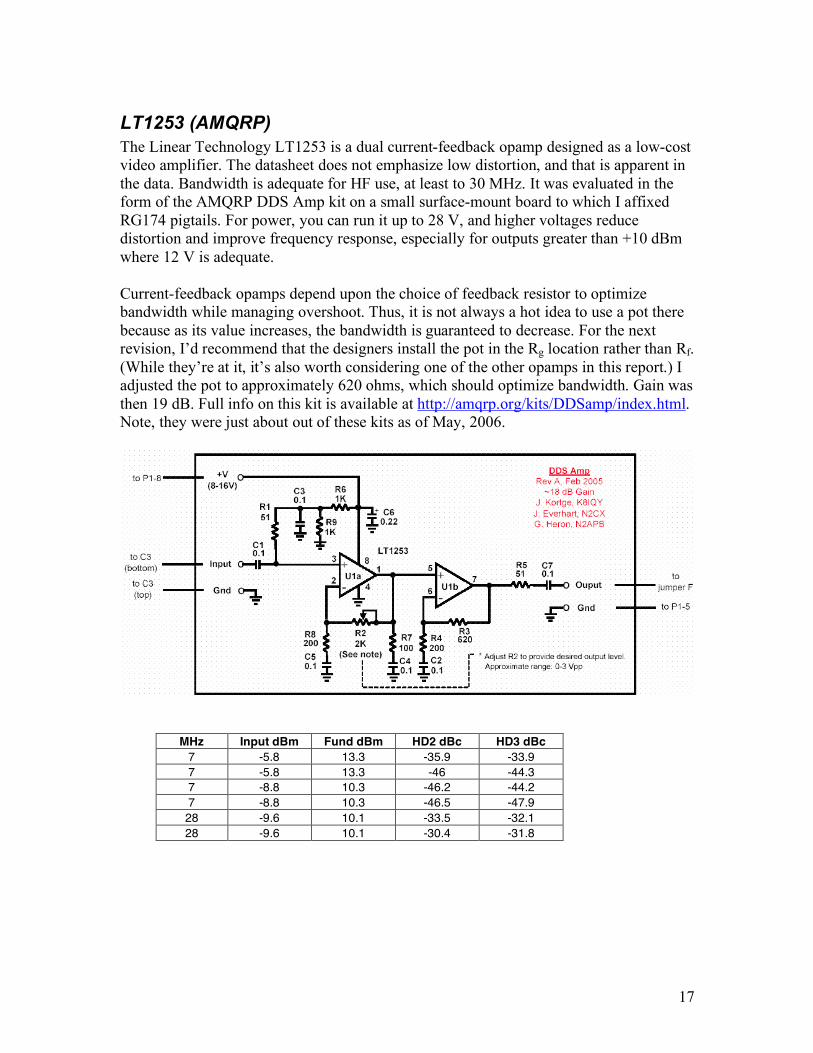
LT1253 (AMQRP) The Linear Technology LT1253 is a dual current-feedback opamp designed as a low-cost video amplifier. The datasheet does not emphasize low distortion, and that is apparent in the data. Bandwidth is adequate for HF use, at least to 30 MHz. It was evaluated in the form of the AMQRP DDS Amp kit on a small surface-mount board to which I affixed RG174 pigtails. For power, you can run it up to 28 V, and higher voltages reduce distortion and improve frequency response, especially for outputs greater than +10 dBm where 12 V is adequate. Current-feedback opamps depend upon the choice of feedback resistor to optimize bandwidth while managing overshoot. Thus, it is not always a hot idea to use a pot there because as its value increases, the bandwidth is guaranteed to decrease. For the next revision, I’d recommend that the designers install the pot in the Rg location rather than Rf. (While they’re at it, it’s also worth considering one of the other opamps in this report.) I adjusted the pot to approximately 620 ohms, which should optimize bandwidth. Gain was then 19 dB. Full info on this kit is available at http://amqrp.org/kits/DDSamp/index.html. Note, they were just about out of these kits as of May, 2006.
MHz Input dBm Fund dBm HD2 dBc HD3 dBc 7 -5.8 13.3 -35.9 -33.9 7 -5.8 13.3 -46 -44.3 7 -8.8 10.3 -46.2 -44.2 7 -8.8 10.3 -46.5 -47.9 28 -9.6 10.1 -33.5 -32.1 28 -9.6 10.1 -30.4 -31.8
18
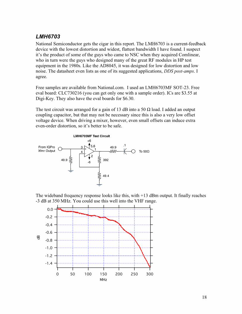
LMH6703 National Semiconductor gets the cigar in this report. The LMH6703 is a current-feedback device with the lowest distortion and widest, flattest bandwidth I have found. I suspect it’s the product of some of the guys who came to NSC when they acquired Comlinear, who in turn were the guys who designed many of the great RF modules in HP test equipment in the 1980s. Like the AD8045, it was designed for low distortion and low noise. The datasheet even lists as one of its suggested applications, DDS post-amps. I agree. Free samples are available from National.com. I used an LMH6703MF SOT-23. Free eval board: CLC730216 (you can get only one with a sample order). ICs are $3.55 at Digi-Key. They also have the eval boards for $6.30. The test circuit was arranged for a gain of 13 dB into a 50 Ω load. I added an output coupling capacitor, but that may not be necessary since this is also a very low offset voltage device. When driving a mixer, however, even small offsets can induce extra even-order distortion, so it’s better to be safe.
The wideband frequency response looks like this, with +13 dBm output. It finally reaches -3 dB at 350 MHz. You could use this well into the VHF range.
-1.4
-1.2
-1.0
-0.8
-0.6
-0.4
-0.2
0.0
dB
300250200150100500
MHz
19
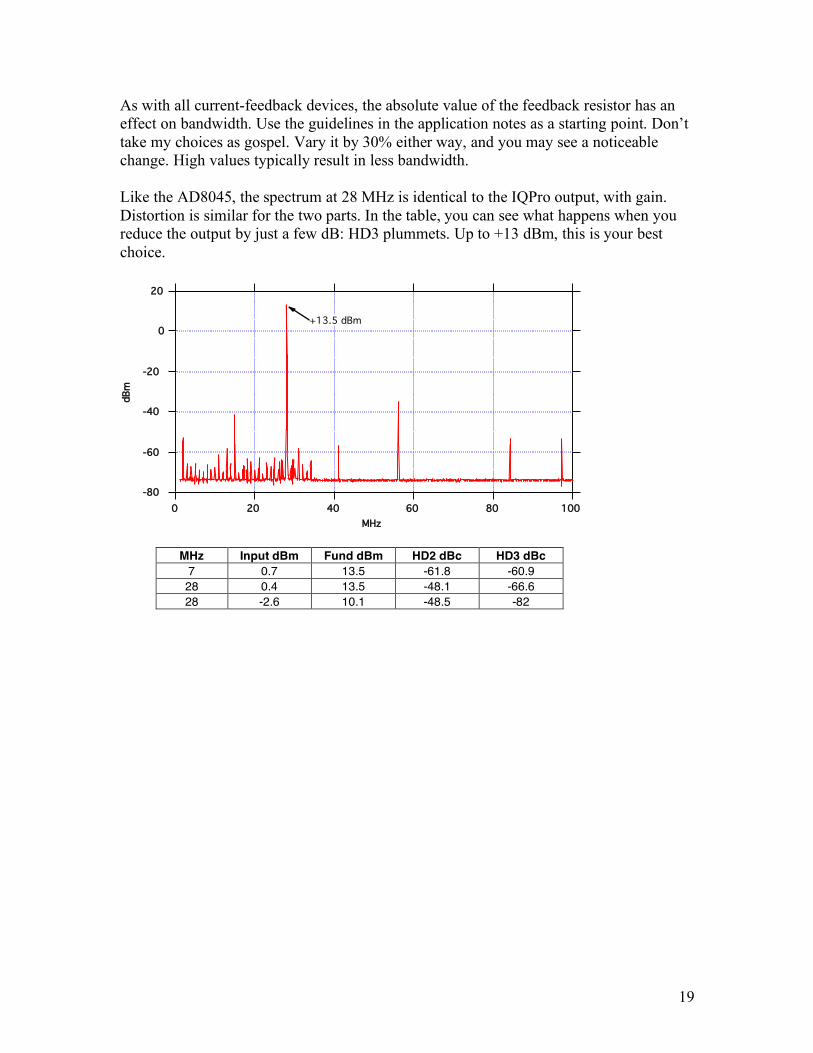
As with all current-feedback devices, the absolute value of the feedback resistor has an effect on bandwidth. Use the guidelines in the application notes as a starting point. Don’t take my choices as gospel. Vary it by 30% either way, and you may see a noticeable change. High values typically result in less bandwidth. Like the AD8045, the spectrum at 28 MHz is identical to the IQPro output, with gain. Distortion is similar for the two parts. In the table, you can see what happens when you reduce the output by just a few dB: HD3 plummets. Up to +13 dBm, this is your best choice.
-80
-60
-40
-20
0
20
dBm
100806040200
MHz
+13.5 dBm
MHz Input dBm Fund dBm HD2 dBc HD3 dBc 7 0.7 13.5 -61.8 -60.9 28 0.4 13.5 -48.1 -66.6 28 -2.6 10.1 -48.5 -82
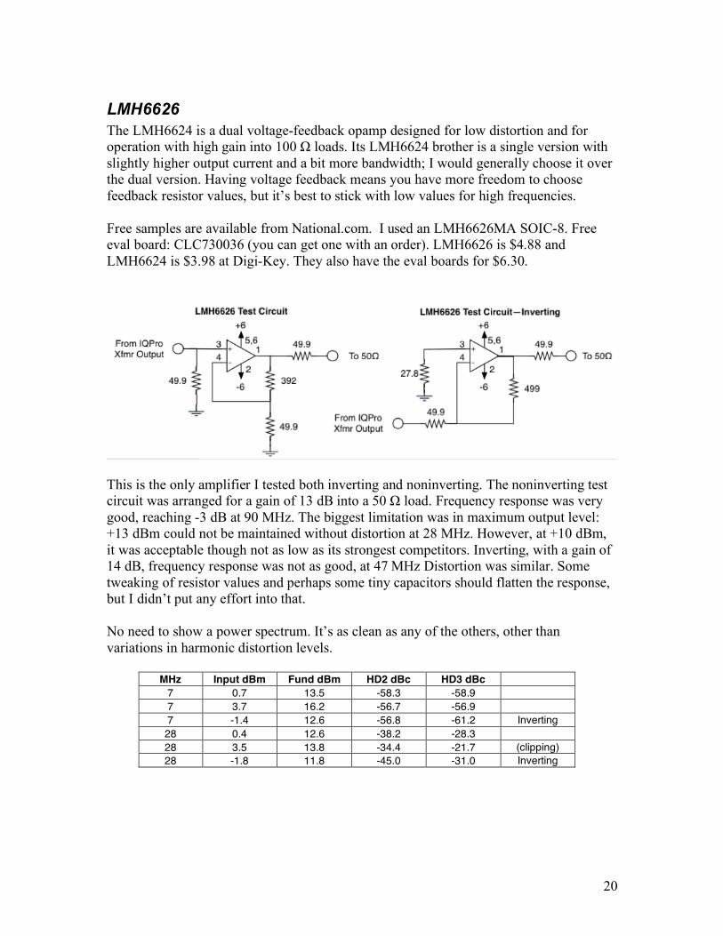
20
LMH6626 The LMH6624 is a dual voltage-feedback opamp designed for low distortion and for operation with high gain into 100 Ω loads. Its LMH6624 brother is a single version with slightly higher output current and a bit more bandwidth; I would generally choose it over the dual version. Having voltage feedback means you have more freedom to choose feedback resistor values, but it’s best to stick with low values for high frequencies. Free samples are available from National.com. I used an LMH6626MA SOIC-8. Free eval board: CLC730036 (you can get one with an order). LMH6626 is $4.88 and LMH6624 is $3.98 at Digi-Key. They also have the eval boards for $6.30.
This is the only amplifier I tested both inverting and noninverting. The noninverting test circuit was arranged for a gain of 13 dB into a 50 Ω load. Frequency response was very good, reaching -3 dB at 90 MHz. The biggest limitation was in maximum output level: +13 dBm could not be maintained without distortion at 28 MHz. However, at +10 dBm, it was acceptable though not as low as its strongest competitors. Inverting, with a gain of 14 dB, frequency response was not as good, at 47 MHz Distortion was similar. Some tweaking of resistor values and perhaps some tiny capacitors should flatten the response, but I didn’t put any effort into that. No need to show a power spectrum. It’s as clean as any of the others, other than variations in harmonic distortion levels.
MHz Input dBm Fund dBm HD2 dBc HD3 dBc 7 0.7 13.5 -58.3 -58.9 7 3.7 16.2 -56.7 -56.9 7 -1.4 12.6 -56.8 -61.2 Inverting 28 0.4 12.6 -38.2 -28.3 28 3.5 13.8 -34.4 -21.7 (clipping) 28 -1.8 11.8 -45.0 -31.0 Inverting
21
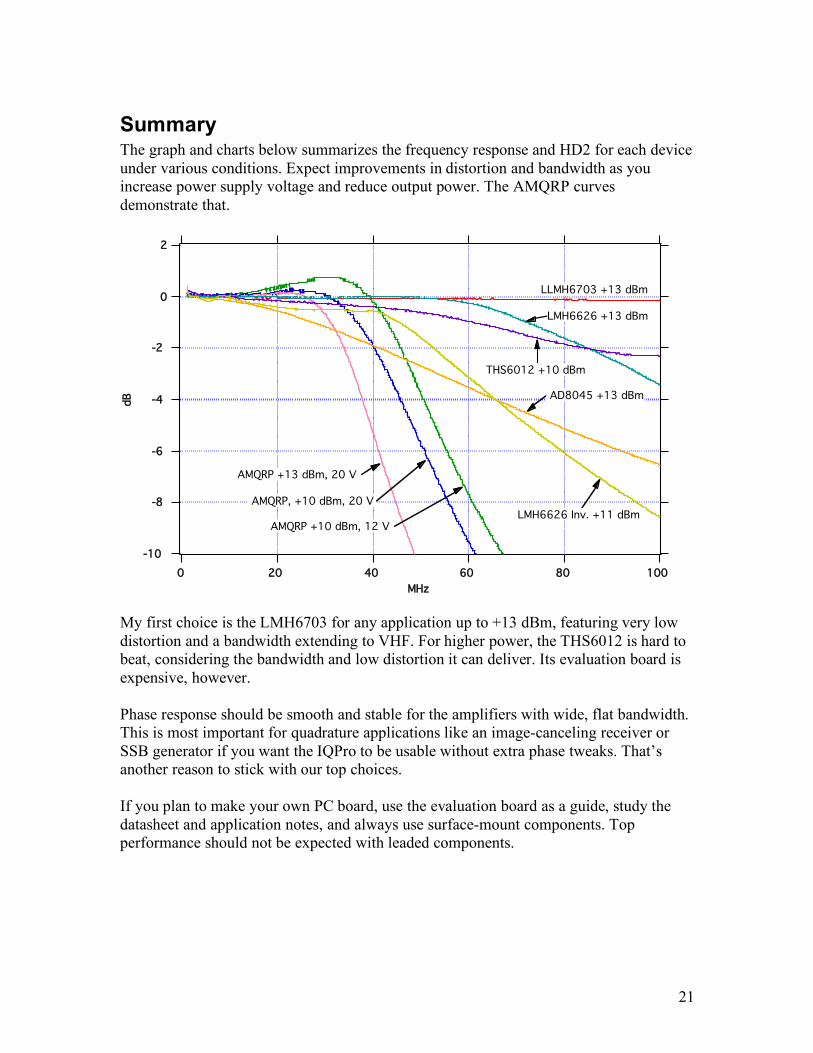
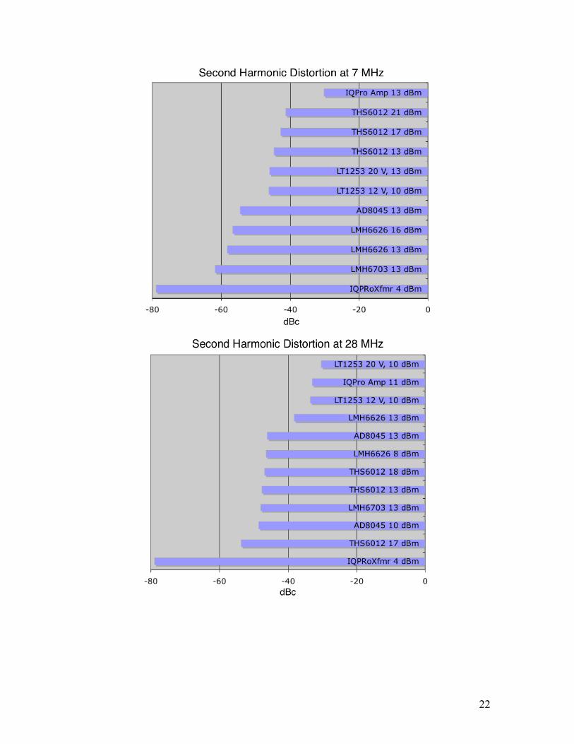
Summary The graph and charts below summarizes the frequency response and HD2 for each device under various conditions. Expect improvements in distortion and bandwidth as you increase power supply voltage and reduce output power. The AMQRP curves demonstrate that.
-10
-8
-6
-4
-2
0
2
dB
100806040200
MHz
LLMH6703 +13 dBm
LMH6626 +13 dBm
THS6012 +10 dBm
LMH6626 Inv. +11 dBm AMQRP +10 dBm, 12 V
AMQRP, +10 dBm, 20 V
AMQRP +13 dBm, 20 V
AD8045 +13 dBm
My first choice is the LMH6703 for any application up to +13 dBm, featuring very low distortion and a bandwidth extending to VHF. For higher power, the THS6012 is hard to beat, considering the bandwidth and low distortion it can deliver. Its evaluation board is expensive, however. Phase response should be smooth and stable for the amplifiers with wide, flat bandwidth. This is most important for quadrature applications like an image-canceling receiver or SSB generator if you want the IQPro to be usable without extra phase tweaks. That’s another reason to stick with our top choices. If you plan to make your own PC board, use the evaluation board as a guide, study the datasheet and application notes, and always use surface-mount components. Top performance should not be expected with leaded components.
22
23
Conclusion The IQPro is a good value and a great springboard for many applications requiring a quadrature source up to 30 MHz. Its transformer-coupled output meets the manufacturer’s specifications and is readily coupled to a variety of post-amplifiers. Unless improvements are made, the built-in transistor amplifier should only be used at low output levels and low frequencies, or in applications that can tolerate higher distortion and additional spurious signals. As with any DDS, be aware of the spurious content and its repercussions in your system. To quote Wes Hayward, W7ZOI, “It certainly illustrates the good characteristics of the DDS synthesizer of low wideband phase noise and reasonable, if not stellar spurious responses.” A number of modern wideband opamps are now available to the amateur at reasonable prices and are easy to use with their evaluation boards. This report should give you some idea of the kind of performance that is achievable, and it is hard to beat at any price. This report will remain a work in progress for some time. I look forward to suggestions and criticisms, and will try to add new data as it becomes available.
About the Author Gary W. Johnson is an instrumentation engineer at the Lawrence Livermore National Laboratory. He has a BS degree in electrical engineering/bioengineering from the University of Illinois. His professional interests include measurement and control systems, electro-optics, communications, transducers, circuit design, and technical writing. He is the author of two books and holds nine patents. In his spare time, he enjoys woodworking, bicycling, and audio. He and his wife, Katharine, a scientific illustrator, live in Livermore, California, with their twin Afghan hounds, Chloe and Derby. His email is [email protected].