Embed Size (px)
Citation preview
14
Performance of Modification of a Three Phase Dynamic Voltage Restorer (DVR)
for Voltage Quality Improvement in Electrical Distribution System
R. Omar1, N.A. Rahim2 and Marizan Sulaiman3
1 Faculty of Electrical, Universiti Teknikal Malaysia Melaka, Durian Tunggal, Melaka, 2Centre of Research for Power Electronics, Drives, Automation and Control
University of Malaya, Kuala Lumpur, 3Faculty of Electrical, Universiti Teknikal Malaysia Melaka, Durian Tunggal, Melaka,
Malaysia
1. Introduction
There is growing concern over power quality of ac supply systems. Power quality can be defined as the ability of utilities to provide electric power without interruption. Various power quality problems can be categorized as voltage sags, swells, harmonics, transients and unbalance are considered are the most common power quality problems in electrical distribution systems (Elandy etl., 2006). These types of disturbances can cause fails in the equipments, raising the possibility of an energy interruption.Voltage swells can be defined as a short duration increase in rms of main source with an increase in voltage ranging from 1.1 p.u up to 1.8 p.u. of nominal voltage source. There are various solutions to these problems. One of the most effective solutions is the installation of a Dynamic Voltage Restorer (DVR) (Alves etl., 1999), (Boonchiam etl., 2006), (Ezoji etl’, 2009), (Banaei etl., 2006).
Traditional DVR (Vilathgamuwa etl., 2002) functions by injecting three single phase AC voltages in series with three-phase incoming voltage during disturbances, compensating for the difference between faulty and nominal voltages. Figure1. where the DVR consists of essentially a series connected injection transformer, a voltage source inverter (VSI), inverter output filter and an energy storage device connected to the dc-link. The power system upstream to DVR is represented by an equivalent voltage source and source impedance. The disturbances correction capability of the restorer depends on the maximum voltage injection capability of the device. In (Elnady etl., 2007) an analysis of the energy requirement of the DVR is presented and a control scheme is proposed. A voltage sag can be defined as a decrease between 0.1 and 0.9 p.u. in the voltage root mean square value at the power frequency for durations from 0.5 cycles to 1 minute (Lam etl., 2008). The widespread use of equipment sensitive to voltage variation, has made industrial applications more susceptible to supply voltage sags. Voltage sags are normally caused by single and three phase fault in the distribution system and by the startup of induction motors of large rating (Wang etl., 2006), (Sanchez etl., 2009). Voltage sags/swells can occurs more frequently than other power quality phenomenon. These sags/swells are the most
www.intechopen.com
Power Quality – Monitoring, Analysis and Enhancement
306
important power quality problems in the power distribution system. IEEE 519-1992 and IEEE 1159-1995 describe the voltage sags/swells as shown in Figure 2 (IEEE Standards 1995), ( Sabin etl., 1996), (Bollen etl., 1999), (Vilathgamuwa etl., 2002).
AC SOURCE
SENSITIVE
LOAD
IMPEDANCE Vinj
VSI
FILTER
CONTROL
CIRCUIT
DVR
ENERGY
STORAGE
VloadVs
Fig. 1. Conventional DVR Circuit Topology (Nielsen etl., 2005)
Voltage Sag
Momentary Temporary
Undervoltage
Tra
nsie
nt
No
tch
/Tra
nsie
nt
Normal Operating Voltage
Swell Overvoltage
Sustianed interuption
Eve
nt
Ma
gn
itu
de
110%
90%
10%
0.5
cycle
3 sec 1min
Event Duration
Fig. 2. Voltage Reduction Standard of IEEE Std 1159-1995
www.intechopen.com
Performance of Modification of a Three Phase Dynamic Voltage Restorer (DVR) for Voltage Quality Improvement in Electrical Distribution System
307
2. Materials and methods
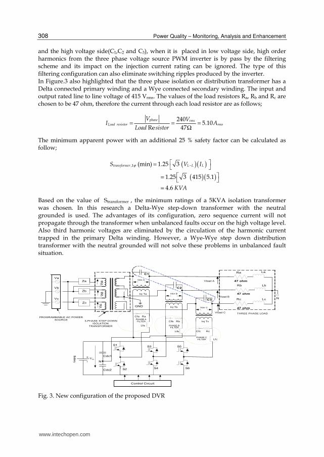
2.1 DVR concept in distribution system Figure. 1 shows a DVR is connected in series between sensitive loads in order to mitigate unbalanced loads or faults in feeder. The possibility of compensation of voltage disturbances can be limited by a number of factors including finite DVR, power rating, different load conditions, background power quality problems and different types of disturbances in the distribution system. There are several types of energy storage been used in the DVR such as battery, superconducting coil, and flywheels. These types of energy storages are very important in order to supply active and reactive power to DVR. The controller is an important part of the DVR for switching purposes. The switching inverter is responsible to do conversion process from DC to AC. The inverter ensures that only the swells or sags voltage is injected to the injection transformer. (Kim etl., 2004),(Sasitharan etl., 2010). In this chapter, a new topology of the DVR is proposed by using a three phase four wire, three phase inverter with six Insulated Gate Bipolar Transistor (IGBTs), DVR with split capacitors (Cdc1 and Cdc2) and new installation of the capacitors filtering scheme. With these new topologies the proposed DVR offers the following advantages over the traditional DVRs:
• A Three phase four wire DVR is used, the beneficial of this configuration is that to control the zero sequence voltage during the unbalanced faults period.
• A three phase DVR with three single phase full bridge inverter has been proposed in the previous DVR. Typically, only one capacitor is used at the dc side of the inverter. In these configuration three control systems and many IGBTs switches are needed, so it’s very costly.
• The placement of the capacitors filter at the high voltage side causes the harmonics for the voltage at the connected load is reduced.
• The DVR with split capacitors (Cdc1 and Cdc2) causes zero sequence current to circulate through the DC –link; therefore unbalanced voltage sags with zero sequence can be compensated effectively.
2.2 The circuit of the proposed topology Four different system topologies for DVRs has been analyzed and tested in (Nielsen etl., 2005). Figure 3 illustrates a new configuration model of the proposed DVR system, and the system consists of a DC voltage source (Vdc), three single phase injection transformer, a three phase voltage source PWM inverter, L-C output filter and sensitive loads. In this proposed designed of DVR, special attention must be paid on three types of configuration as follows;
• Filtering schemes configuration
• Isolation or distribution transformer and
• Injection transformer winding. Filtering configuration for DVR is very important as it related with the system dynamic response. The filtering system of the DVR can be placed either on the high voltage or the low-voltage side of the injection transformer and are referred to as line side filter and inverter-side filter respectively. (Kim etl., 2004), (Sasitharan etl., 2010). In the proposed filtering system as shown in Figure 3, the filtering scheme is installed for both on the low and high voltages. The filter inductor, capacitor and resistor (Lfa,Lfb,Lfc ,Cfa,Cfb,Cfc and Ra,Rb,Rc) are installed on low voltage side between the series inverter and the transformer
www.intechopen.com
Power Quality – Monitoring, Analysis and Enhancement
308
and the high voltage side(C1,C2 and C3), when it is placed in low voltage side, high order harmonics from the three phase voltage source PWM inverter is by pass by the filtering scheme and its impact on the injection current rating can be ignored. The type of this filtering configuration can also eliminate switching ripples produced by the inverter. In Figure.3 also highlighted that the three phase isolation or distribution transformer has a Delta connected primary winding and a Wye connected secondary winding. The input and output rated line to line voltage of 415 Vrms. The values of the load resistors Ra, Rb and Rc are chosen to be 47 ohm, therefore the current through each load resistor are as follows;
phase rmsLoad resistor rms
V VI A
Load sistor
2405.10
Re 47= = =
Ω
The minimum apparent power with an additional 25 % safety factor can be calculated as follow;
( )( )
( )( )
transformer L L LS V I
KVA
,1 (min) 1.25 3
1.25 3 415 5.1
4.6
ϕ − = =
=
Based on the value of Stransformer , the minimum ratings of a 5KVA isolation transformer was chosen. In this research a Delta-Wye step-down transformer with the neutral grounded is used. The advantages of its configuration, zero sequence current will not propagate through the transformer when unbalanced faults occur on the high voltage level. Also third harmonic voltages are eliminated by the circulation of the harmonic current trapped in the primary Delta winding. However, a Wye-Wye step down distribution transformer with the neutral grounded will not solve these problems in unbalanced fault situation.
Vdc
Za
Zb
Zc
Cfa
Cfb
Cfc
Ra
Rb
Rc
Inj Ta
Inj Tb
Inj Tc
C1
C2
C3
Lfa
Lfb
Lfc
S1S3 S5
S2 S4 S6
3-PHASE STEP DOWN
ISOLATION
TRANSFORMER
PROGRAMMABLE AC POWER
SOURCE
Control Circuit
Cdc1
Battery
PHASE A
FILTER
PHASE BFILTER
PHASE CFILTER
Va
Vb
Vc
Vsb
Vsc
Vload A
Vload B
Vload C
Vdvr A
Vdvr B
Vdvr C
Vsa
Ra La
Rb
Rc Lc
Lb
47 ohm
47 ohm
47 ohm
N
THREE PHASE LOAD
Cdc2
N
GND
Fig. 3. New configuration of the proposed DVR
www.intechopen.com
Performance of Modification of a Three Phase Dynamic Voltage Restorer (DVR) for Voltage Quality Improvement in Electrical Distribution System
309
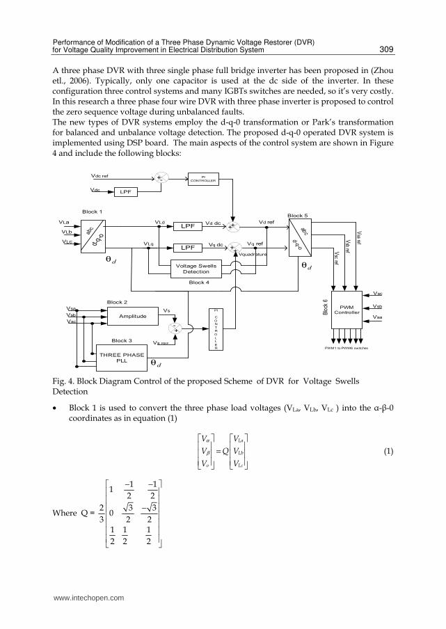
A three phase DVR with three single phase full bridge inverter has been proposed in (Zhou etl., 2006). Typically, only one capacitor is used at the dc side of the inverter. In these configuration three control systems and many IGBTs switches are needed, so it’s very costly. In this research a three phase four wire DVR with three phase inverter is proposed to control the zero sequence voltage during unbalanced faults. The new types of DVR systems employ the d-q-0 transformation or Park’s transformation for balanced and unbalance voltage detection. The proposed d-q-0 operated DVR system is implemented using DSP board. The main aspects of the control system are shown in Figure 4 and include the following blocks:
abc
LPF
LPF
LPF
VLa
VLb
VLc
THREE PHASE
PLL
+
++
+
d-q-oabc
Amplitude
Vsa
Vsb
Vsc-+
PI
C
ON
TR
O
LL
ER
Vs REF
VsPWM
ControllerVsa
Vsb
Vsc
+-PI
CONTROLLER
Vdc
VLd
VLq Vq dc
Vd dc
Vq ref
Vd ref
Vsa
ref
Vsb
refVsc
ref
Vdc ref
Block 1
Block 2
Block 3
Block 5
Blo
ck 6
Voltage Swells
Detection
Block 4
PWM1 to PWM6 switches
d-q-
o
Vquadrature
dθdθ
dθ
Fig. 4. Block Diagram Control of the proposed Scheme of DVR for Voltage Swells Detection
• Block 1 is used to convert the three phase load voltages (VLa, VLb, VLc ) into the ┙-┚-0 coordinates as in equation (1)
La
Lb
o Lc
V V
V Q V
V V
α
β
=
(1)
Where Q =
1 11
2 2
2 3 30
3 2 21 1 1
2 2 2
− − −
www.intechopen.com
Power Quality – Monitoring, Analysis and Enhancement
310
• Block 1 is also used to convert the three phase load voltages (VLa, VLb, VLc ) into the ┙-┚-o coordinates as in equation (1), the three phase load voltages reference components V┙-
ref, V┙-ref and Vo ref can be converted to Vd ref and Vq ref as shown in equation (2).
d
q
V V
V V
cos sin
2
sin cos3
α
β
θ θ
θ θ
= − (2)
Transformation to dqo to abc
d
q
V V
V V
cos sin
2
sin cos3
α
β
θ θ
θ θ
− = (3)
a
b
c o
V V
V V
V V
1 0 1
30.5 1
2
30.5 1
2
α
β
= −
−
(4)
• Block 2 is considered as a source voltages (Vsa, Vsb, Vsc). The amplitude of AC voltage at the sources (Vsource) can be calculated as shown in equation (5);
( ) ( ) ( )source sa sb scV V V V2 2 22
3
= + + (5)
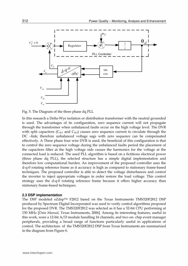
Block 3 is a three phase PLL (Phase-locked loop). PLL comprises a Phase Detection (PD) scheme, a Loop Filter (LF), and a Voltage Controlled Oscillator (VCO). The phase difference between the input and the output signals is measured using a phase detection scheme and passed through a loop filter to generate an error signal driving a voltage-controlled oscillator (VCO) which generates the output signal. The PLL block is implemented in d-q-0 synchronous reference frame as shown in Figure 5. The PLL block allows to detect the amplitude and phase (Vs and θ ) of fundamental positive sequence components of the
source voltages. A PI regulator is used to control this variable and the output of this regulator is the source frequency,the source voltage angle can be obtained through the
integration of the source frequency. The PLL output ( dθ ) is an estimation of the source angle
to the fundamental frequency. Let us detail the PLL block as shown in Fig.5(a). Let the measured network voltages at the Point Common Coupling (PCC) are given by VPCC (a,b,c) could be converted to the d-q-0 dynamic reference frame VPCC (d,q,0) using the Park Transformation as follow:
( ) ( )PCC PCCV d q S V a b c, ,0 , ,= • (6)
www.intechopen.com
Performance of Modification of a Three Phase Dynamic Voltage Restorer (DVR) for Voltage Quality Improvement in Electrical Distribution System
311
where S = can be defined as:
1 1 1
2 2 2
2 2 2S cos cos cos
3 3 3
2 2sin sin sin
3 3
π πθ θ θ
π πθ θ θ
= − + − − − − +
(7)
The input voltage is considered sinusoidal with amplitude V, then:
( )
( )s
PCC
PCC PCC s
PCC
s
V tV a
V a b c V b V t
V c
V t
,
,
,
sin
2, , sin
3
2sin
3
ω φ
πω φ
πω φ
+ = = + − + +
(8)
The value of stω φ+ in (8) can be replaced by sθ , equations (8) and (6) could be substituted
in equation (7), the below expression is obtained after rejecting the homopolar component
since it not be used[18],
( )( )
( )s dPCC
PCC
PCC s d
V dV d q V
V q
,
,
sin3,
2 cos
θ θ
θ θ
− = = − − (9)
( )( )
( )PCC
PCC
PCC
V dV d q V
V q
,
,
sin3,
2 cos
θ
θ
Δ = = − Δ (10)
Where ( )s dθ θ θΔ = −
The supply voltages will be locked by the PLL if there is an error between the phase of the
supply voltage and the output of the PLL system is equal zero, in the case of θΔ = 0 Block 4 is the detection scheme for the voltage Unbalanced compensator. From Figure 5
shows that, the synchronous frame variables, Vd and Vq are used as inputs for low pass
filters to generate voltage references in the synchronous frame. Block 5 receive the
components of the load voltage vectors Vd ref and Vq ref and transforms them to three
phase coordinates using equation (3) and (4) the generation voltages are used as the
voltage reference. The DC link error in Figure 4 is used to get optimized controller output
signal because the energy on the DC link will be changed during the unbalance voltage.
Block 6 is the PWM block, this block provides the firing for the Inverter switches (PWM1 to
PWM6). The injection voltage is generated according to the difference between the
reference load voltage and the supply voltage and is applied to the voltage source Inverter
(VSI).
www.intechopen.com
Power Quality – Monitoring, Analysis and Enhancement
312
Regulator
PLL Controller
+-
sin
cos
saV
sbV
scV
dθs
10≡∗
dV
ffω
dV
qV
++
abcd-q-o
Fig. 5. The Diagram of the three phase dq PLL
In this research a Delta-Wye isolation or distribution transformer with the neutral grounded
is used. The advantages of its configuration, zero sequence current will not propagate
through the transformer when unbalanced faults occur on the high voltage level. The DVR
with split capacitors (Cdc1 and Cdc2) causes zero sequence current to circulate through the
DC –link; therefore unbalanced voltage sags with zero sequence can be compensated
effectively. A Three phase four wire DVR is used, the beneficial of this configuration is that
to control the zero sequence voltage during the unbalanced faults period the placement of
the capacitors filter at the high voltage side causes the harmonics for the voltage at the
connected load is reduced. The used PLL algorithm is based on a fictitious electrical power
(three phase dq PLL), the selected structure has a simple digital implementation and
therefore low computational burden. An improvement of the proposed controller uses the
d-q-0 rotating reference frame as it accuracy is high as compared to stationary frame-based
techniques. The proposed controller is able to detect the voltage disturbances and control
the inverter to inject appropriate voltages in order restore the load voltage. This control
strategy uses the d-q-0 rotating reference frame because it offers higher accuracy than
stationary frame-based techniques.
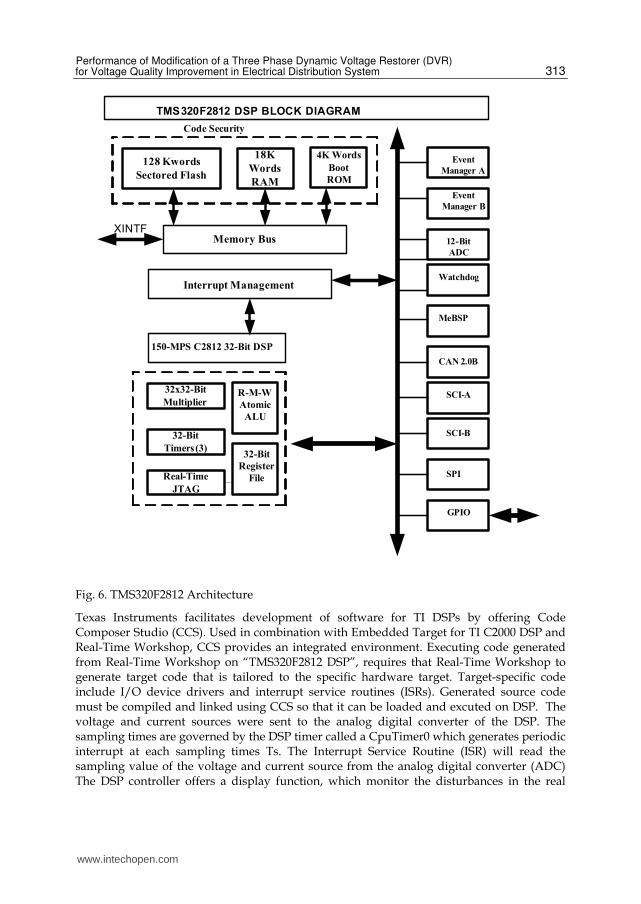
2.3 DSP implementation The DSP modeled eZdspTM F2812 based on the Texas Instruments TMS320F2812 DSP
produced by Spectrum Digital Incorporated was used to verify control algorithms proposed
for the proposed DVR. The TMS320F2812 was selected as it has a 32-bit CPU performing at
150 MHz [Data Manual, Texas Instruments, 2006]. Among its interesting features, useful in
this work, were a 12-bit A/D module handling 16 channels, and two on- chip event manager
peripherals, providing a broad range of functions particularly useful in applications of
control. The architecture of the TMS320F2812 DSP from Texas Instruments are summarized
in the diagram from Figure 6.
www.intechopen.com
Performance of Modification of a Three Phase Dynamic Voltage Restorer (DVR) for Voltage Quality Improvement in Electrical Distribution System
313
128 Kwords
Sectored Flash
18K
Words
RAM
TMS320F2812 DSP BLOCK DIAGRAM
Code Security
4K Words
Boot
ROM
Memory Bus
Event
Manager B
Event
Manager A
12-Bit
ADC
Watchdog
GPIO
Interrupt Management
32x32-Bit
Multiplier
150-MPS C2812 32-Bit DSP
32-Bit
Timers(3)
Real-Time
JTAG
CAN 2.0B
MeBSP
SCI-A
SCI-B
SPI
R-M-W
Atomic
ALU
32-Bit
Register
File
XINTF
Fig. 6. TMS320F2812 Architecture
Texas Instruments facilitates development of software for TI DSPs by offering Code Composer Studio (CCS). Used in combination with Embedded Target for TI C2000 DSP and Real-Time Workshop, CCS provides an integrated environment. Executing code generated from Real-Time Workshop on “TMS320F2812 DSP”, requires that Real-Time Workshop to generate target code that is tailored to the specific hardware target. Target-specific code include I/O device drivers and interrupt service routines (ISRs). Generated source code must be compiled and linked using CCS so that it can be loaded and excuted on DSP. The voltage and current sources were sent to the analog digital converter of the DSP. The sampling times are governed by the DSP timer called a CpuTimer0 which generates periodic interrupt at each sampling times Ts. The Interrupt Service Routine (ISR) will read the sampling value of the voltage and current source from the analog digital converter (ADC) The DSP controller offers a display function, which monitor the disturbances in the real
www.intechopen.com
Power Quality – Monitoring, Analysis and Enhancement
314
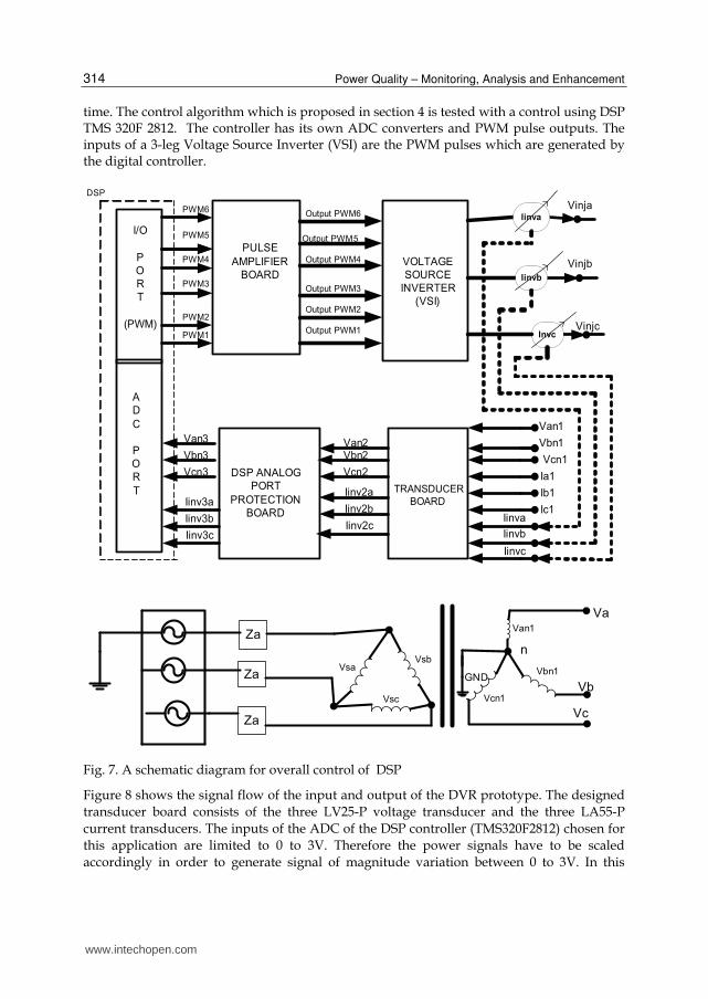
time. The control algorithm which is proposed in section 4 is tested with a control using DSP TMS 320F 2812. The controller has its own ADC converters and PWM pulse outputs. The inputs of a 3-leg Voltage Source Inverter (VSI) are the PWM pulses which are generated by the digital controller.
PULSE
AMPLIFIER
BOARD
VOLTAGE
SOURCE
INVERTER
(VSI)
TRANSDUCER
BOARD
DSP
DSP ANALOG
PORT
PROTECTION
BOARD
I/O
P
O
R
T
(PWM)
Van1
Vbn1
Vcn1
Ia1
Ib1
Ic1
Vinja
Vinjb
Vinjc
Iinva
Van2Vbn2
Vcn2Vcn3
Vbn3
Output PWM6PWM6
PWM5
Iinv2a
Iinv2b
Iinv2c
Van3
Iinv3a
Iinv3b
Iinv3c
Iinvc
Iinvb
Iinva
A
D
C
P
O
R
T
PWM4
PWM3
PWM2
PWM1
Output PWM5
Output PWM4
Output PWM3
Output PWM2
Output PWM1
Iinva
Iinvb
Invc
GNDVsa
Za
Za
Za
Vsb
Vsc
Van1
Vcn1
Vbn1
Va
Vb
Vc
n
Fig. 7. A schematic diagram for overall control of DSP
Figure 8 shows the signal flow of the input and output of the DVR prototype. The designed
transducer board consists of the three LV25-P voltage transducer and the three LA55-P
current transducers. The inputs of the ADC of the DSP controller (TMS320F2812) chosen for
this application are limited to 0 to 3V. Therefore the power signals have to be scaled
accordingly in order to generate signal of magnitude variation between 0 to 3V. In this
www.intechopen.com
Performance of Modification of a Three Phase Dynamic Voltage Restorer (DVR) for Voltage Quality Improvement in Electrical Distribution System
315
application the voltage and current transducers are used to scale down and convert the
signals to a ground referenced signal suitable for the DSP. A power supply of a 5V is
required to power both the voltage and current transducers for their operation. The three
source side terminal voltages between the line and neutral Van1,Vbn1 and Vcn1 from the
transformer in Figure 8 are measured by three of the voltage transducers LV25-P. The
inverter output currents Iinva, Iinvb, Iinvc from the Voltage Source Inverter (VSI) are also
detected by the three of current transducers LA55-P. The inverter currents are used to boost
up the voltage response of the DVR. The three source voltages and the inverter output
currents are entered to DSP through the DSP Analog Port Protection Board. The output
signals of the transducer board as shown in Figure 8 must be fed into the DSP Analog Port
Protection Board before connecting them to the ADC port of the DSP. This is to ensure that
the DSP board is protected from any over voltage that may occur during signal acquisition.
The line currents Ia1, Ib1 and Ic1 control independently of the three phase voltage signals
Van1, Vbn1 and Vcn1 to ensure the VSI can operate properly and avoid it from damage. The
whole control system was coded by C language and compiled into DSP board. The ADC
port of the DSP board receives all these signals from the DSP Analog Port Protection Board
and it will process the sampled voltage and current signals. Six digital PWM pulses are
produced via I/O Port (PWM) and the output signals of the I/O Port (PWM) are passed
through to a Pulse Amplifier Board. The Pulse Amplified Board is needed to up the PWM
digital signals to the voltage level required by the VSI. The VSI will produce the three phase
output voltages required for voltage disturbances mitigation.
3. Results and discussion
The system modeled in Figure 3 has been simulated using Matlab/Simulink. The
performance of the system has been considered with the load is represented by a series
equivalent rated at 415Vrms, 5KVA at 0.95 load power factor. Simulation and experimental
parameters are given in Table 1. The performance of the DVR for different supply
disturbances is tested under various operating conditions. Several simulation of the DVR
with proposed controller scheme and new configuration of it have been made.
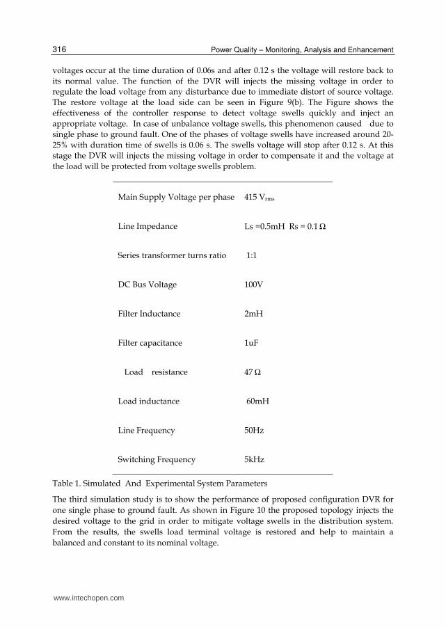
As for the filtering scheme is placed in the high voltage side in this case, high order
harmonic currents will penetrates through the injection transformer and it will carry the
harmonic voltages. Fast Fourier Transform (FFT) analyses for the output voltage at the
connected load has been done without or with capacitors filter (C1, C2 and C3) at the high
voltage level side of the transformer as shown in Figure 8. Figure.8 (a) shows that FFT
analysis when the transformer at the high voltage level is not installed with the capacitors
filter. The Total Harmonics Distortion (THD) for the voltage is about 33.29% ,when the
capacitors filter are placed at the high level side, THD value decreases to 2.34% as shown in
Figure. 8(b). Thus the harmonics are reduced from 33.29 % to 2.34%. The THD value of 2.34
% when capacitors filter are placed at the high voltage transformer side is satisfying the
IEEE-519 standard harmonic voltage limit.
Investigation on the DVR performance can be observed through testing under various
disturbances condition on the source voltage. The proposed control algorithm was tested for
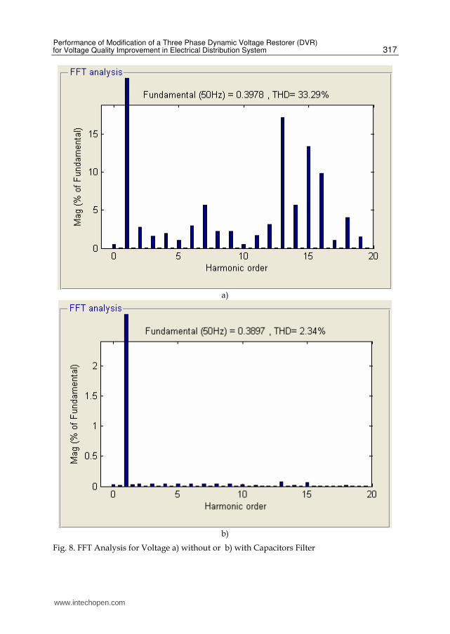
balanced and unbalanced voltages swells in the low voltage distribution system. In case of
balance voltage swell, the source voltage has increased about 20-25% of its nominal value.
The simulation results of the balance voltage swells as shown in Figure 9(a). The swells
www.intechopen.com
Power Quality – Monitoring, Analysis and Enhancement
316
voltages occur at the time duration of 0.06s and after 0.12 s the voltage will restore back to
its normal value. The function of the DVR will injects the missing voltage in order to
regulate the load voltage from any disturbance due to immediate distort of source voltage.
The restore voltage at the load side can be seen in Figure 9(b). The Figure shows the
effectiveness of the controller response to detect voltage swells quickly and inject an
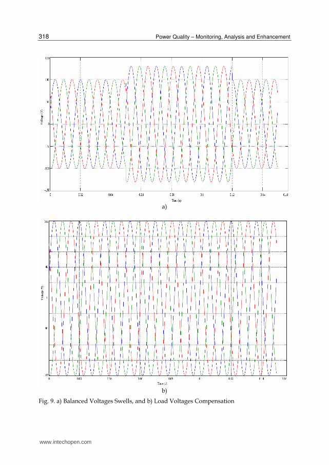
appropriate voltage. In case of unbalance voltage swells, this phenomenon caused due to
single phase to ground fault. One of the phases of voltage swells have increased around 20-
25% with duration time of swells is 0.06 s. The swells voltage will stop after 0.12 s. At this
stage the DVR will injects the missing voltage in order to compensate it and the voltage at
the load will be protected from voltage swells problem.
Main Supply Voltage per phase 415 Vrms
Line Impedance Ls =0.5mH Rs = 0.1 Ω
Series transformer turns ratio 1:1
DC Bus Voltage 100V
Filter Inductance 2mH
Filter capacitance 1uF
Load resistance 47 Ω
Load inductance 60mH
Line Frequency 50Hz
Switching Frequency 5kHz
Table 1. Simulated And Experimental System Parameters
The third simulation study is to show the performance of proposed configuration DVR for
one single phase to ground fault. As shown in Figure 10 the proposed topology injects the
desired voltage to the grid in order to mitigate voltage swells in the distribution system.
From the results, the swells load terminal voltage is restored and help to maintain a
balanced and constant to its nominal voltage.
www.intechopen.com
Performance of Modification of a Three Phase Dynamic Voltage Restorer (DVR) for Voltage Quality Improvement in Electrical Distribution System
317
a)
b)
Fig. 8. FFT Analysis for Voltage a) without or b) with Capacitors Filter
www.intechopen.com
Power Quality – Monitoring, Analysis and Enhancement
318
a)
b)
Fig. 9. a) Balanced Voltages Swells, and b) Load Voltages Compensation
www.intechopen.com
Performance of Modification of a Three Phase Dynamic Voltage Restorer (DVR) for Voltage Quality Improvement in Electrical Distribution System
319
a)
b)
Fig. 10. a) One Phase Voltage Swells, and b) Voltage Swells after Compensation
www.intechopen.com
Power Quality – Monitoring, Analysis and Enhancement
320
a)
b)
c)
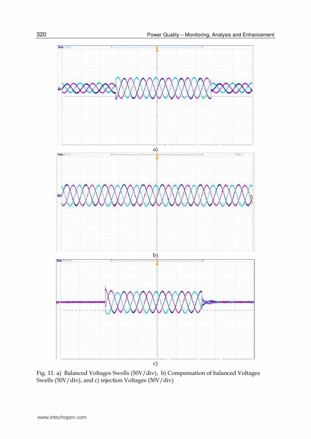
Fig. 11. a) Balanced Voltages Swells (50V/div), b) Compensation of balanced Voltages Swells (50V/div), and c) injection Voltages (50V/div)
www.intechopen.com
Performance of Modification of a Three Phase Dynamic Voltage Restorer (DVR) for Voltage Quality Improvement in Electrical Distribution System
321
a)
b)
c)
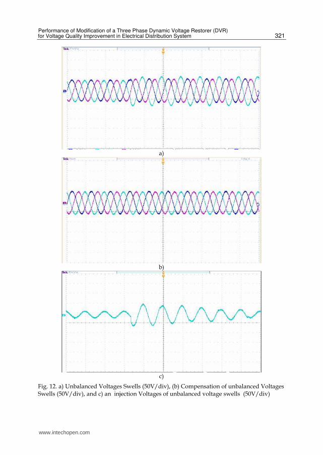
Fig. 12. a) Unbalanced Voltages Swells (50V/div), (b) Compensation of unbalanced Voltages Swells (50V/div), and c) an injection Voltages of unbalanced voltage swells (50V/div)
www.intechopen.com
Power Quality – Monitoring, Analysis and Enhancement
322
a) b)
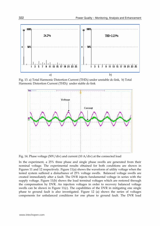
Fig. 13. a) Total Harmonic Distortion Current (THDI) under unstable dc-link, b) Total Harmonic Distortion Current (THDI) under stable dc-link
Fig. 14. Phase voltage (50V/div) and current (10 A/div) at the connected load
In the experiment, a 25% three phase and single phase swells are generated from their nominal voltage. The experimental results obtained for both conditions are shown in Figures 11 and 12 respectively. Figure 11(a) shows the waveform of utility voltage when the tested system suffered a disturbance of 25% voltage swells. Balanced voltage swells are created immediately after a fault. The DVR injects fundamental voltage in series with the supply voltage. Figure 11(b) shows the load terminal voltages which are restored through the compensation by DVR. An injection voltages in order to recovery balanced voltage swells can be shown in Figure 11(c). The capabilities of the DVR in mitigating one single phase to ground fault is also investigated. Figure 12 (a) shows the series of voltages components for unbalanced conditions for one phase to ground fault. The DVR load
www.intechopen.com
Performance of Modification of a Three Phase Dynamic Voltage Restorer (DVR) for Voltage Quality Improvement in Electrical Distribution System
323
voltages are shown in Figure 12 (b). As can be seen the swells load terminal voltage is compensated and help to maintain a balanced and constant load voltage and the control method that can generate the required voltages from significantly disturbance source voltages. Figure 12(c) shows the injection voltage of a single phase swells. As shown in Figure 3 there are two DC-link capacitors were used, it acts as an energy storage element of the DVR. The rating of the IGBT is totally depending on the DC link of the DVR prototype. Harmonic current is depending on the DC link voltage. The function of the DC link is to absorb the ripple, therefore the values of the DC side capacitors (Cdc1 and Cdc2) should be large enough without the distorting the dc bus voltage much. If there is distortion in the dc voltage the inverter output will get distorted with third harmonic content. With the stability of the DC bus and the Total Harmonic Distortion for current (THDI) for third harmonics current is reduced 24.2 % to 2.23% as shown in Figure. 13(a) and 13(b). Phase voltage and current at the load are the sinusoidal waveform without any distortion due to design of the good capacitor filter and use of the suggested controller, this can be seen in Figure 14.
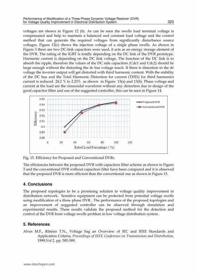
Fig. 15. Efficiency for Proposed and Conventional DVRs
The efficiencies between the proposed DVR with capacitors filter scheme as shown in Figure 3 and the conventional DVR without capacitors filter have been compared and it is observed that the proposed DVR is more efficient than the conventional one as shown in Figure 15.
4. Conclusions
The proposed topologies to be a promising solution to voltage quality improvement in distribution network. Sensitive equipment can be protected from potential voltage swells using modification of a three phase DVR . The performance of the proposed topologies and an improvement of suggested controller can be observed through simulation and experimental results. These results validate the proposed method for the detection and control of the DVR from voltage swells problem in low voltage distribution system.
5. References
Alves M.F., Ribeiro T.N., Voltage Sag an Overview of IEC and IEEE Standards and Application Criteria, Proceedings of IEEE Conference on Transmission and Distribution, 1999,Vol 2. pp. 585-589.
www.intechopen.com
Power Quality – Monitoring, Analysis and Enhancement
324
Banaei M.R., Hosseini S.H., Khanmohamadi S. and Gharehpetian G.B.,Verification of a New Energy Control Strategy for Dynamic Voltage Restorer by simulation, ELSEVIER Simulation Modeling Practice and Theory, 14(2006),pp. 113-125.
Boonchiam P., and Mithulananthan N., Dynamic Control Strategy in Medium Voltage DVR for Mitigating Voltage Sags/Swells International Conference on Power System Technology, 2006, pp. 1-5.
Elnady A. and Salama M.M. A., Mitigation of Voltage disturbances using adaptive perception –based control algorithm, IEEE Trans. Power Delivery., vol. 20, no.1, pp,309-318, Jan.2005.
Elnady, A., and Salama, M.M. A: Mitigation of Voltage Disturbances Using Adaptive Perceptron-Based Control Algorithm, IEEE , Transactions on Power Delivery, 2005, 20, (1),pp, 309-318.
Ezoji, A. Sheikholeslami, Tabasi M. and Saeednia M.M., Simulation Of Dynamic Voltage Restorer Using Hysteresis Voltage Control, European Journal of Scientific Research (EJSR), 27(1) (2009), pp. 152-166.
IEEE Standards Board (1995), IEEE Std. 1159-1995, IEEE Recommended Practice for Monitoring Electric Power Quality. IEEE Inc. New York.
Kim H, Kim J H and Sul S K, A Design Consideration of Output Filters for dynamic Voltage Restorer. 35th Annual IEEE Power Electronic Specialist Conference 2004.
Lam C.S., Wong M.C., and Han Y.D., Voltage swell and over-voltage compensation with unidirectional power flow controlled dynamic voltage restorer, IEEE Trans. Power Delivery., vol.23, no.4, pp. 2513-2521, Oct. 2008.
MS320F2812 Digital Signal Processors, Data Manual, Texas Instruments, 2006. Nielsen J.G. and Blaabjerg F., A Detailed Comparison of system J Topologies for Dynamic
Voltage Restorer, IEEE Transaction on Industrial Applications, vol.41, no.5, Sept/Oct.2005, pp.1272-1280.
Sabin D., An assessment of distribution system power quality, Elect.Power Res. Inst., Palo Alto, CA, EPRI Final Rep. TR-106294-V2, vol. 2, Statistical Summary Report, May 1996.
Sanchez P.R., Acha E., Calderon J.E.O., Feliu V., and Cerada A.G., A versatile control scheme for a dynamic voltage restorer for a dynamic voltage restorer for power quality improvement, IEEE Trans. Power Delivery., vol. 24, no.1, pp. 277-284 Jan. 2009.
Sasitharan S., Mahesh K. Mishra, B. Kalyan Kumar, V. Jayashankar, Rating and design issues of DVR injection transformer. International Journal of Power Electronics 2010 - Vol. 2, No.2 pp. 143 – 163.
Vilathgamuwa M., Ranjith Pcrcra A. A. D. and Choi S. S., Performance improvcmcnt of the dynamic voltage restorer with closed-loop load voltage and current-mode control, IEEE Transactions on PowerElectronics, vol. 17, no. 5, Sept. 2002, pp. 824-834.
Wang B., Venkataramanan G., and IIIindala M., Operation and control of a dynamic voltage restorer using transformer coupled H-bridge converter, IEEE Trans. Power Electron.,vol.21, no.4, pp. 1053-1061 Jul. 2006.
Zhou G., Shi X, Fu C. and Wang Y., Operation of a Three phase Soft Phase Locked Loop Under Distorted Voltage Conditions Using Intelligent PI Controller, in Proc. 2006 IEEE Region 10 Conf. (TENCON 2006), pp 315-320.
www.intechopen.com
Power Quality – Monitoring, Analysis and EnhancementEdited by Dr. Ahmed Zobaa
ISBN 978-953-307-330-9Hard cover, 364 pagesPublisher InTechPublished online 22, September, 2011Published in print edition September, 2011
InTech EuropeUniversity Campus STeP Ri Slavka Krautzeka 83/A 51000 Rijeka, Croatia Phone: +385 (51) 770 447
InTech ChinaUnit 405, Office Block, Hotel Equatorial Shanghai No.65, Yan An Road (West), Shanghai, 200040, China Phone: +86-21-62489820 Fax: +86-21-62489821
This book on power quality written by experts from industries and academics from various counties will be ofgreat benefit to professionals, engineers and researchers. This book covers various aspects of power qualitymonitoring, analysis and power quality enhancement in transmission and distribution systems. Some of the keyfeatures of books are as follows: Wavelet and PCA to Power Quality Disturbance Classification applying a RBFNetwork; Power Quality Monitoring in a System with Distributed and Renewable Energy Sources; SignalProcessing Application of Power Quality Monitoring; Pre-processing Tools and Intelligent Techniques forPower Quality Analysis; Single-Point Methods for Location of Distortion, Unbalance, Voltage Fluctuation andDips Sources in a Power System; S-transform Based Novel Indices for Power Quality Disturbances; LoadBalancing in a Three-Phase Network by Reactive Power Compensation; Compensation of Reactive Power andSag Voltage using Superconducting Magnetic Energy Storage; Optimal Location and Control of Flexible ThreePhase Shunt FACTS to Enhance Power Quality in Unbalanced Electrical Network; Performance of Modificationof a Three Phase Dynamic Voltage Restorer (DVR) for Voltage Quality Improvement in Distribution System;Voltage Sag Mitigation by Network Reconfiguration; Intelligent Techniques for Power Quality Enhancement inDistribution Systems.
How to referenceIn order to correctly reference this scholarly work, feel free to copy and paste the following:
R. Omar, N.A. Rahim and Marizan Sulaiman (2011). Performance of Modification of a Three Phase DynamicVoltage Restorer (DVR) for Voltage Quality Improvement in Electrical Distribution System, Power Quality– Monitoring, Analysis and Enhancement, Dr. Ahmed Zobaa (Ed.), ISBN: 978-953-307-330-9, InTech,Available from: http://www.intechopen.com/books/power-quality-monitoring-analysis-and-enhancement/performance-of-modification-of-a-three-phase-dynamic-voltage-restorer-dvr-for-voltage-quality-improv
www.intechopen.com

Fax: +385 (51) 686 166www.intechopen.com
Fax: +86-21-62489821

© 2011 The Author(s). Licensee IntechOpen. This chapter is distributedunder the terms of the Creative Commons Attribution-NonCommercial-ShareAlike-3.0 License, which permits use, distribution and reproduction fornon-commercial purposes, provided the original is properly cited andderivative works building on this content are distributed under the samelicense.


![dynamic voltage regulator-2[1]](https://img.pdfslide.us/doc/110x75/5516be0d4a79593e218b4572/dynamic-voltage-regulator-21.jpg)