Embed Size (px)
Citation preview
Performance Evaluation and Comparative
Study of Different High-K Poly-Si and Metal
Gate Stack in MOSFET
Seema Verma1, Pooja Srivastava
2, Shailja Yadav
3, Tanushree Bhadouria
4, Aunnaty Puri
5, Urvashi Vishnoi
6
1Associate Professor, Department of Electronics, Banasthali University, Rajasthan, India
2Assistant Professor, Department of Electronics, Banasthali University, Rajasthan, India
3,4,5,6Student, M.Tech. (VLSI Design), Banasthali University, Rajasthan, India
Abstract-The unceasing demand of miniaturization has
reduced the SiO2 gate dielectric layer thickness to
nearly 5 atomic layers. Oxide breakdown due to hot
electron tunneling is a critical concern at this level as it
contributes to gate current leakage through the gate.
Any further scaling is bound to increase the already
tricky gate current leakage and lead to more power loss,
increased power consumption and excessive heat
generation. Materials with high dielectric constant, K,
are required to reduce leakage and improve
performance. In this paper, the use of High K dielectric
material Hafnium Oxide (HfO2) over SiO2 as dielectric
and metal gate over poly-Si gate were compared.
Keywords-High K Material, Poly-Si Gate stack, Metal
Gate Stack, Hafnium Oxide
I. INTRODUCTION
The need of increased speed at constant power has
led to shrinking of MOSFET dimensions as well as
oxide thickness as per scaling rules dictate as shown
in Fig. 1.
Fig. 1. MOSFET Gate Thickness Trend [10]
The silicon industry has scaled down silicon-dioxide
aggressively for past several years to achieve smaller
and even smaller devices. The continual reduction of
gate oxide thickness has led to drastic increase in gate
oxide leakage. Eventually this incessant scaling of
MOSFET would lead to such reduction in physical
thickness of SiO2 that this layer would run out of
atoms for further scaling.
In order to meet the Moore’s prediction for further
scaling MOSFET need High-K gate dielectrics with
high thickness to reduce leakage power. High-K gate
dielectric materials have held the promise of
continued scaling with low gate leakage current [2].
The challenges with the usage of High-K dielectric
material include Fermi Level Pinning [3], Phonon
Scattering, Poly Depletion [9] and Poor Reliability
[12]. These effects are found to be higher with Poly-
Si gate than metal gate structure. When metal gates
were used with High-K dielectrics, they not only
eliminate Poly Depletion Effects but also Phonon
Degradation thus led to better performance. In this
paper, we had studied the simple MOSFET structure
with SiO2-Poly-Si Gate Stack, HfO2-Poly-Si Gate
Stack, and HfO2-TiN-Metal Gate Stack.
II. NEED FOR HIGH K
“K” indicates the amount of charge a material can
easily hold when used as dielectric. "High-K"
materials [1], such as Hafnium Oxide (HfO2),
Zirconium Dioxide (ZrO2) and Titanium Dioxide
(TiO2) inherently have “K” above 3.9, which is “K”
for silicon dioxide [4].
International Journal of Scientific & Engineering Research, Volume 6, Issue 2, February-2015 ISSN 2229-5518 1
IJSER © 2015 http://www.ijser.org
IJSER
The drain current ID for a MOSFET in linear region
of operation [5] can be approximated as follows by
Eq. 1
ID = µCOXW/2L[2(Vgs-VT)Vds- Vds2] (1)
The drain current ID for a MOSFET in saturation
region of operation [5] can be approximated as
follows by Eq. 2
ID = µCOXW/2L[Vgs-VT]2 (2)
μ is carrier mobility, COX represents the capacitance
of gate dielectric, Vgs is gate-source voltage applied,
VT is the threshold gate-source voltage required to
turn on the MOSFET and Vds is drain-source voltage
applied. It can be seen that drain current ID can be
increased by decreasing the channel length or by
increasing the capacitance. The capacitance of the
gate can be modeled as a parallel-plate capacitor as
described by Eq. 3 as follows
C = Kε0A/t (3)
A is the area of the capacitor and t is the thickness of
dielectric with Dielectric constant, K. Since the
thickness is to be greater for these new dielectrics, it
requires an even larger K so as to increase the overall
capacitance – that is where these High-K dielectric
materials come into play.
III. THE OBSERVED DESIGN
We took in consideration three different models of
transistors at 0.1 µm level: SiO2 dielectric with Poly-
Si gate (T1), HfO2 dielectric with Poly-Si gate (T2),
HfO2 dielectric with TiN metal gate (T3) to discover
the advantages of HfO2 over SiO2 dielectric and also
the advantages of metal gate over Poly-Si for High-K
materials [6].
IV. COMPARATIVE STUDY
The comparison between Structure T1, Structure T2
and Structure T3 is explained as follows.
A. Comparison Between SiO2 and HfO2 as dielectric
The capacitance of High-K dielectric was observed to
be roughly 60% greater than that of SiO2 which
resulted in drastic reduction in gate electric leakage
with low power dissipation and faster response time.
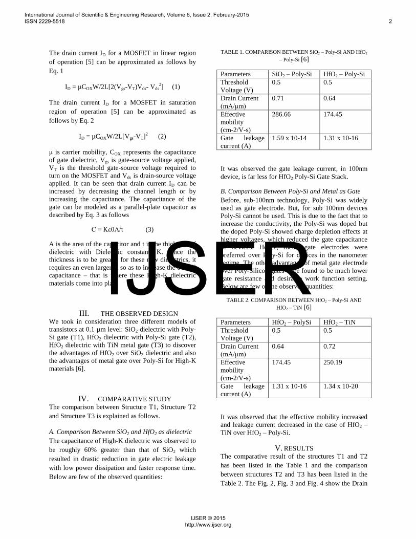
Below are few of the observed quantities:
TABLE 1. COMPARISON BETWEEN SiO2 – Poly-Si AND HfO2
– Poly-Si [6]
Parameters SiO2 – Poly-Si HfO2 – Poly-Si
Threshold
Voltage (V)
0.5
0.5
Drain Current
(mA/μm)
0.71 0.64
Effective
mobility
(cm-2/V-s)
286.66
174.45
Gate leakage
current (A)
1.59 x 10⁻¹⁴
1.31 x 10⁻¹⁶
It was observed the gate leakage current, in 100nm
device, is far less for HfO2 Poly-Si Gate Stack.
B. Comparison Between Poly-Si and Metal as Gate
Before, sub-100nm technology, Poly-Si was widely
used as gate electrode. But, for sub 100nm devices
Poly-Si cannot be used. This is due to the fact that to
increase the conductivity, the Poly-Si was doped but
the doped Poly-Si showed charge depletion effects at
higher voltages, which reduced the gate capacitance
of devices. Hence, metal gate electrodes were
preferred over Poly-Si for devices in the nanometer
regime. The other advantages of metal gate electrode
over Poly-Silicon gates were found to be much lower
gate resistance and desirable work function setting.
Below are few of the observed quantities:
TABLE 2. COMPARISON BETWEEN HfO2 – Poly-Si AND
HfO2 – TiN [6]
Parameters HfO2 – PolySi HfO2 – TiN
Threshold
Voltage (V)
0.5 0.5
Drain Current
(mA/μm)
0.64 0.72
Effective
mobility
(cm-2/V-s)
174.45
250.19
Gate leakage
current (A)
1.31 x 10⁻¹⁶
1.34 x 10⁻²⁰
It was observed that the effective mobility increased
and leakage current decreased in the case of HfO2 –
TiN over HfO2 – Poly-Si.
V. RESULTS
The comparative result of the structures T1 and T2
has been listed in the Table 1 and the comparison
between structures T2 and T3 has been listed in the
Table 2. The Fig. 2, Fig. 3 and Fig. 4 show the Drain
International Journal of Scientific & Engineering Research, Volume 6, Issue 2, February-2015 ISSN 2229-5518 2
IJSER © 2015 http://www.ijser.org
IJSER
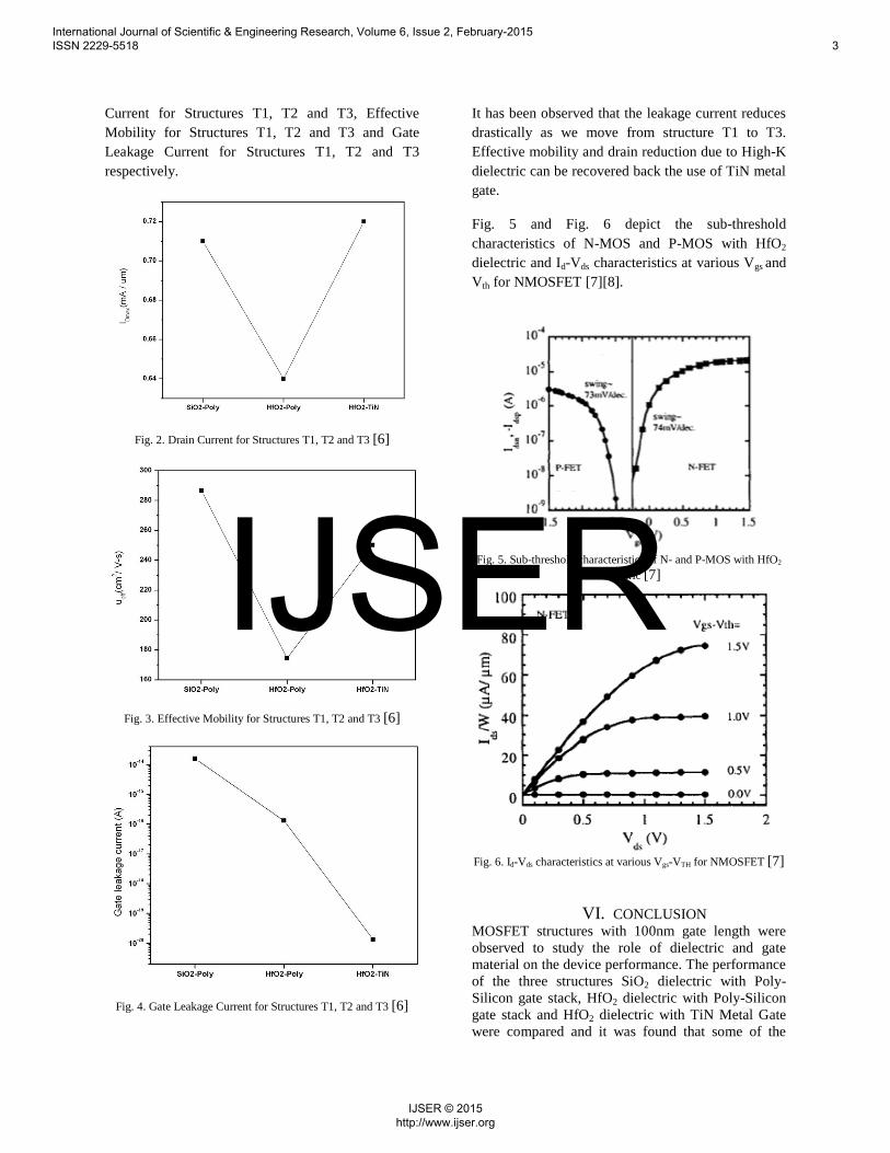
Current for Structures T1, T2 and T3, Effective
Mobility for Structures T1, T2 and T3 and Gate
Leakage Current for Structures T1, T2 and T3
respectively.
Fig. 2. Drain Current for Structures T1, T2 and T3 [6]
Fig. 3. Effective Mobility for Structures T1, T2 and T3 [6]
Fig. 4. Gate Leakage Current for Structures T1, T2 and T3 [6]
It has been observed that the leakage current reduces
drastically as we move from structure T1 to T3.
Effective mobility and drain reduction due to High-K
dielectric can be recovered back the use of TiN metal
gate.
Fig. 5 and Fig. 6 depict the sub-threshold
characteristics of N-MOS and P-MOS with HfO2
dielectric and Id-Vds characteristics at various Vgs and
Vth for NMOSFET [7][8].
Fig. 5. Sub-threshold characteristics of N- and P-MOS with HfO2
dielectric [7]
Fig. 6. Id-Vds characteristics at various Vgs-VTH for NMOSFET [7]
VI. CONCLUSION
MOSFET structures with 100nm gate length were
observed to study the role of dielectric and gate
material on the device performance. The performance
of the three structures SiO2 dielectric with Poly-
Silicon gate stack, HfO2 dielectric with Poly-Silicon
gate stack and HfO2 dielectric with TiN Metal Gate
were compared and it was found that some of the
International Journal of Scientific & Engineering Research, Volume 6, Issue 2, February-2015 ISSN 2229-5518 3
IJSER © 2015 http://www.ijser.org
IJSER
parameters like drain current, and mobility which
degraded with the use of High-K dielectric were
improved back again by replacing Poly-Silicon gate
by Metal gate. Drastic reduction in gate leakage
current projects the High K–Metal Gate technology
to be a strong yet unconventional substitute for the
SiO2-Poly-Si structure for the nano-scale regime
MOS devices. As the technology advances by an
incredible speed, the scope of accurate and smaller
devices to operate low battery gadgets is greater than
ever. This requirement seems to be satisfied with
High K- Metal gate technology [11].
VII. FUTURE SCOPE
High-K dielectric have been studied as a substitute
for SiO2 dielectric layer but there are still many
unanswered challenges that need to be addressed and
discussed. Some of which are Fermi Level Pinning
[3][14][12] due to High K material, Mobility
Degradation, Phonon Scattering, Reliability
Improvement [15] as well as the optimized process of
fabrication.
VIII. ACKNOWLEDGEMENT
This work is supported by Department of Electronics,
Banasthali University, Rajasthan, India.
REFERENCES
[1] S. Natarajan et. al., “A 32nm Logic Technology
Featuring 2nd Generation High-k Metal-Gate
Transistors, Enhanced Channel Strain and 0.171µm2
SRAM Cell Size in a 291Mb Array”, IEDM Tech.
Digest, 2008
[2] K.Mistry et. al. “A 45nm Logic Technology with
High-k Metal Gate Transistors, Strained Silicon, 9 Cu
Interconnect Layers, 193nm Dry Patterning, and
100% Pb-free Packaging” IEDM Tech. Digest, p.
247, 2007
[3] C.Hobbs et al., “Fermi Level Pinnig at the Poly-
Si/Metal Oxide In Trace”, in Symposium VLSI Tech.
Digest, pp .9-10, 2003
[4] Yudong Kim, et. al. “Conventional n-channel
MOSFET devices using single layer HfO2 and ZrO2
as high-k gate dielectrics with polysilicon gate
electrode”, IEDM Tech. Digest, pp. 247, 2007
[5] Sung-Mo Kang, Yusuf Leblebici, “CMOS Digital
Integrated Circuit”, third edition, Tata McGraw Hill
2012
[6] Shashank N, S Basak, R K Nahar, “Design and
Simulation of Nano Scale High-K Based MOSFETs
with Poly Silicon and Metal Gate Electrodes”
International Journal of Advancement in Technology
Vol 1, No 2 (October 2010)
[7] Laegu Kang, et. al. “MOSFET Devices with
Polysilicon on Single-Layer Hf02 High-K
Dielectrics”, Electron Devices Meeting, IEDM Tech.
Digest, 2000
[8] Robert Chau, Suman Datta, Mark Doczy, Brian
Doyle, Jack Kavalieros, and Matthew Metz, “High-
K Metal–Gate Stack and Its MOSFET
Characteristics” Volume 25 No. 6 june 2004
[9] Chang-Hoon Choi, “Gate Length Dependent
Polysilicon Depletion Effects”, IEEE Electron
Device Letters, Vol. 23, No. 4, April 2002
[10] B. H. Lee et al., “Gate Stack Technology for
Nano-Scale Devices” Materials Today, Vol. 9, No. 6
p.32-40, June 2006
[11] Jack C. Lee, et. al. “High-K Dielectrics and
MOSFET Characteristics”, IEDM Tech Digest, 2003
[12] Yi-Lin Yang, et. al. “Reliability Improvement of
28-nm High-k /Metal Gate MOSFET Using
Appropriate Oxygen Annealing”, IEEE electron
device letters, vol. 33, no. 8, August 2012
[13] H.-S. P. Wong, “Beyond the Conventional
Transistor”, IBM J Res. and Dev. 46, 133-168, 2002
[14] M. Kadoshima et. al. “Fermi-level Pinning
position modulation by Al-containing metal gate for
cost-effective dual-metal/dual-high-k CMOS”,
Symposium on VLSI Technology Digest of
Technical Papers, 2007
[15] Andreas Kerber and Eduard Albert Cartier
“Reliability Challenges for CMOS Technology
Qualifications with Hafnium Oxide/Titanium Nitride
Gate Stacks”, IEEE transactions on device and
materials reliability, Vol. 9, No. 2, June 2009
[16] Hiroshi Iwai, “High-k/Metal Gate Technology”,
Frontier Research Center, Tokyo Institute of
Technology, January 9, 2008 at IIT-Bombay
International Journal of Scientific & Engineering Research, Volume 6, Issue 2, February-2015 ISSN 2229-5518 4
IJSER © 2015 http://www.ijser.org
IJSER