Embed Size (px)
Citation preview
www.ijsret.org
50 International Journal of Scientific Research Engineering & Technology (IJSRET), ISSN 2278 – 0882
Volume 4, Issue 1, January 2015
PERFORMANCE ANALYSIS OF SEVEN LEVEL INVERTER WITH
SOFT SWITCHING CONVERTER FOR PHOTOVOLTAIC SYSTEM
M.Vidhya1, Dr.P.Radika
2, Dr.J.Baskaran
3
1PG Scholar, Dept.of EEE, Adhiparasakthi Engineering College, Melmaruvathur, Tamilnadu, India 2Professor, Dept.of EEE, Adhiparasakthi Engineering College, Melmaruvathur, Tamilnadu, India
3HOD, Dept. of EEE, Adhiparasakthi Engineering College, Melmaruvathur, Tamilnadu, India
ABSTRACT This paper analyse the performance of Seven Level
Inverter which is configured by means of capacitor
selection circuit and an H- bridge inverter. Multicarrier
Sinusoidal Phase Disposition Pulse Width Modulation
(MCSPDPWM) and Variable Frequency Inverted
Sinusoidal PWM technique (VFISPWM) are employed
for analysing the Total Harmonic Distortion (THD) of
the Seven Level output. The capacitor selection circuit
converts the output of the Soft Switching Interleaved
Boost Converter and solar source into three level direct
current (DC) voltage and an H- bridge inverter further
converts three level dc voltage to seven level
alternating current (AC) voltage.
The performance parameters like output voltage and
efficiency of two different Soft Switching Interleaved
Boost Converters are compared and analysed with the
conventional Interleaved Boost Converter.
Keywords- Soft Switching Interleaved
BoostConverter,Efficiency,Multilevel Inverter, Pulse
Width Modulation technique, Total Harmonic
Distortion (THD)
I. INTRODUCTION Electric power is the most commonly used type of
energy. The use of fossil fuels results in the global
problem of greenhouse emissions. Moreover the cost
of fossil fuel keeps increasing as the supplies of fossil
fuels are depleted in the future.
Thus solar energy is becoming more important
since it produces less pollution. The power conversion
interface is important because it converts the dc power
generated by the solar cell array into ac power and
feeds the utility.
An inverter is necessary in the power conversion
interface to convert the direct current (DC) into
alternating current (AC).Since the output voltage from
the solar cell array is not sufficient enough to be given
as input to the inverter circuit, a soft switching
interleaved boost converter is used. The converter
boost the solar cell output so that it can match with the
dc bus voltage. Here soft switching interleaving boost
converter has been discussed with two different
topologies and compared with conventional
interleaved boost converter to obtain high voltage gain
and efficiency. Multicarrier Sinusoidal PWM
technique and Variable Frequency Inverted Sinusoidal
PWM technique are employed to analyse the Total
Harmonic Distortion of seven level output
waveform.Seven level inverter with only six power
electronic switches was proposed [4]. Hence switching
losses are reduced. Two dc–dc converters are used to
step the output voltage of solar array which leads to
complexity of the circuit. Transformer based converter
are used which reduces the power efficiency.One H-
bridge inverter and two diodeembedded bidirectional
switches was proposed [8] to produce seven level. The
number of diodes are increased which leads to
complex circuit.However three capacitors are used to
produce the voltage levels.Hence balancing the
voltages across three capacitors is more complex. A
five level diode clamped multilevel inverter was
proposed [3]. A separate dc voltage balancing circuit
was equipped to maintain and balance the capacitor
voltage. Coupled inductor is also used in the balancing
circuit and the amplitude of flux will be reduced by
means of the voltage balancing circuit. An interleaved
boost converter with a capacitor for battery charger
applications was proposed [13]. The capacitor is used
for soft switching purpose to reduce the voltage stress
of the converter switches and also to improve the
efficiency. An interleaved boost converter with zero -
voltage transition was proposed [14]. The inductor is
used for the soft switching phenomenon to reduce the
voltage stress and also to improve the conversion
efficiency. Seven level inverter topology with ten
power electronic switches and three capacitors was
proposed [6].Balancing of capacitor voltage becomes
complex and also switching loss increases due to more
number of switches.
II. PROPOSED METHODOLOGY This paper proposes a seven level inverter which is fed
by a solar input source. The input from the solar is
stepped up by means of soft switching interleaved
boost converter. This paper compares operation of
conventional interleaved boost converter with two
different topologies. Topology 1 demonstrates
theoperation of interleaved boost converter with soft
www.ijsret.org
51 International Journal of Scientific Research Engineering & Technology (IJSRET), ISSN 2278 – 0882
Volume 4, Issue 1, January 2015
switching inductor and topology 2 deals with the
operation of interleaved boost converter with soft
switching capacitor. Multicarrier Sinusoidal Phase
Disposition PWM and Variable Frequency Inverted
Sinusoidal PWM techniques are used for the
generation of gate pulses for the inverter switches and
the THD of the seven level output voltage are
analysed. The circuit diagram of conventional
interleaved boost converter is shown in Fig.1
Fig. 1 Circuit Diagram of Conventional Interleaved
Boost Converter
Topology 1: (Soft switched inductor)
The circuit diagram of topology 1 shows the two
shunted boost conversion units and a soft
switching inductor is used to improve the efficiency
and also to increase the output voltage. Fig. 2 shows
the circuit diagram of topology 1
Fig. 2 Circuit Diagram of Topology 1
Topology 2: (Soft switched capacitor)
The circuit diagram of topology 2 shows the two
shunted boost converter units and a soft switching
capacitor to improve the efficiency and also to increase
the output voltage. The circuit diagram of topology 2 is
shown in Fig. 3
Fig. 3 Circuit Diagram of Topology 2
Proposed Seven Level Inverter with Topology 2
(Capacitor)
The proposed seven level is fed by means of solar
input through a soft switching interleaving boost
converter. The seven level inverter consists of a
capacitor selection circuit and full bridge inverter
connected in cascade. The solar input is given to the
capacitor C1 and output from the converter is given to
the capacitor C2.The capacitor selection circuit
converts the input dc voltage into three level dc
voltage and inverter further converts the three level dc
voltage into seven level ac output voltage. The circuit
diagram of proposed seven level inverter is shown in
Fig. 4
Fig.4 Circuit Diagram of Seven Level Inverter with
Topology 2
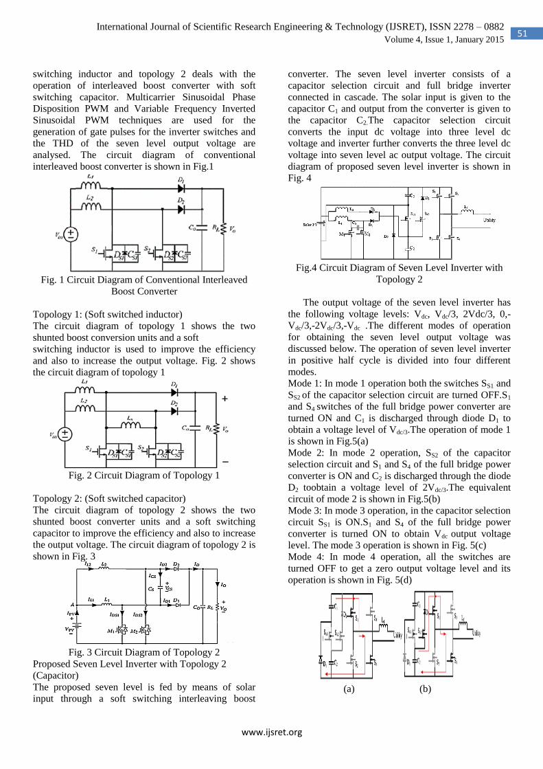
The output voltage of the seven level inverter has
the following voltage levels: Vdc, Vdc/3, 2Vdc/3, 0,-
Vdc/3,-2Vdc/3,-Vdc .The different modes of operation
for obtaining the seven level output voltage was
discussed below. The operation of seven level inverter
in positive half cycle is divided into four different
modes.
Mode 1: In mode 1 operation both the switches SS1 and
SS2 of the capacitor selection circuit are turned OFF.S1
and S4 switches of the full bridge power converter are
turned ON and C1 is discharged through diode D1 to
obtain a voltage level of Vdc/3.The operation of mode 1
is shown in Fig.5(a)
Mode 2: In mode 2 operation, SS2 of the capacitor
selection circuit and S1 and S4 of the full bridge power
converter is ON and C2 is discharged through the diode
D2 toobtain a voltage level of 2Vdc/3.The equivalent
circuit of mode 2 is shown in Fig.5(b)
Mode 3: In mode 3 operation, in the capacitor selection
circuit SS1 is ON.S1 and S4 of the full bridge power
converter is turned ON to obtain Vdc output voltage
level. The mode 3 operation is shown in Fig. 5(c)
Mode 4: In mode 4 operation, all the switches are
turned OFF to get a zero output voltage level and its
operation is shown in Fig. 5(d)
(a) (b)
www.ijsret.org
52 International Journal of Scientific Research Engineering & Technology (IJSRET), ISSN 2278 – 0882
Volume 4, Issue 1, January 2015
(c) (d)
Fig. 5 Operation of different modes in positive half
cycle (a) Mode 1 (b) mode 2 (c) mode 3 (d) mode 4
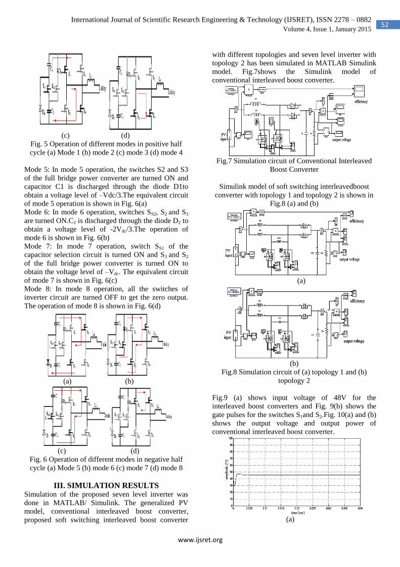
Mode 5: In mode 5 operation, the switches S2 and S3
of the full bridge power converter are turned ON and
capacitor C1 is discharged through the diode D1to
obtain a voltage level of –Vdc/3.The equivalent circuit
of mode 5 operation is shown in Fig. 6(a)
Mode 6: In mode 6 operation, switches SS2, S2 and S3
are turned ON.C2 is discharged through the diode D2 to
obtain a voltage level of -2Vdc/3.The operation of
mode 6 is shown in Fig. 6(b)
Mode 7: In mode 7 operation, switch SS1 of the
capacitor selection circuit is turned ON and S3 and S2
of the full bridge power converter is turned ON to
obtain the voltage level of –Vdc. The equivalent circuit
of mode 7 is shown in Fig. 6(c)
Mode 8: In mode 8 operation, all the switches of
inverter circuit are turned OFF to get the zero output.
The operation of mode 8 is shown in Fig. 6(d)
(a) (b)
(c) (d)
Fig. 6 Operation of different modes in negative half
cycle (a) Mode 5 (b) mode 6 (c) mode 7 (d) mode 8
III. SIMULATION RESULTS Simulation of the proposed seven level inverter was
done in MATLAB/ Simulink. The generalized PV
model, conventional interleaved boost converter,
proposed soft switching interleaved boost converter
with different topologies and seven level inverter with
topology 2 has been simulated in MATLAB Simulink
model. Fig.7shows the Simulink model of
conventional interleaved boost converter.
Fig.7 Simulation circuit of Conventional Interleaved
Boost Converter
Simulink model of soft switching interleavedboost
converter with topology 1 and topology 2 is shown in
Fig.8 (a) and (b)
(a)
(b)
Fig.8 Simulation circuit of (a) topology 1 and (b)
topology 2
Fig.9 (a) shows input voltage of 48V for the
interleaved boost converters and Fig. 9(b) shows the
gate pulses for the switches S1and S2.Fig. 10(a) and (b)
shows the output voltage and output power of
conventional interleaved boost converter.
(a)
www.ijsret.org
53 International Journal of Scientific Research Engineering & Technology (IJSRET), ISSN 2278 – 0882
Volume 4, Issue 1, January 2015
(b)
Fig. 9(a) Input voltage and (b) gate trigger pulses for
the switches
(a)
(b)
Fig. 10(a) Output voltage and (b) Output power of
conventional Interleaved boost converter
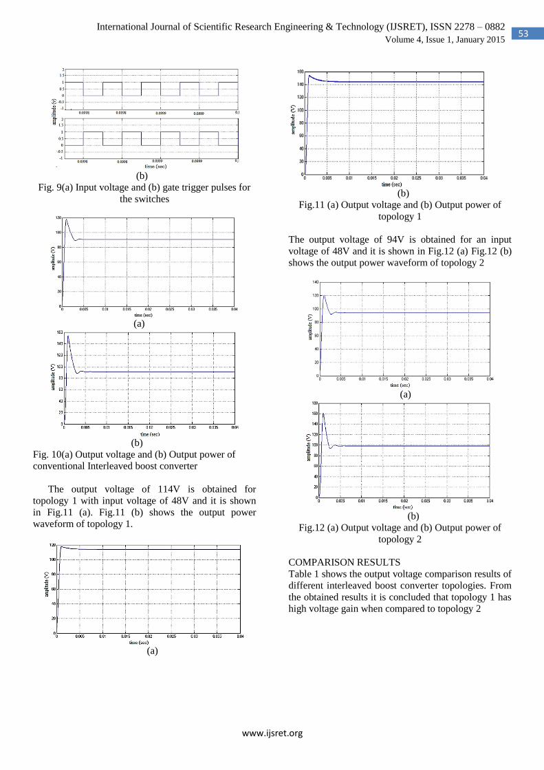
The output voltage of 114V is obtained for
topology 1 with input voltage of 48V and it is shown
in Fig.11 (a). Fig.11 (b) shows the output power
waveform of topology 1.
(a)
(b)
Fig.11 (a) Output voltage and (b) Output power of
topology 1
The output voltage of 94V is obtained for an input
voltage of 48V and it is shown in Fig.12 (a) Fig.12 (b)
shows the output power waveform of topology 2
(a)
(b)
Fig.12 (a) Output voltage and (b) Output power of
topology 2
COMPARISON RESULTS
Table 1 shows the output voltage comparison results of
different interleaved boost converter topologies. From
the obtained results it is concluded that topology 1 has
high voltage gain when compared to topology 2

www.ijsret.org
54 International Journal of Scientific Research Engineering & Technology (IJSRET), ISSN 2278 – 0882
Volume 4, Issue 1, January 2015
TABLE 1: Output voltage comparison of two
interleaved boost converters
Table 2 shows the efficiency comparison results of
different interleaved boost converters. The obtained
results shows that topology 2 has better efficiency
when compared to topology 1 and the efficiency
increases in the order of 0.65 to 0.75%
TABLE 2: Efficiency comparison results of two
interleaved boost converters
Fig.13 shows the Simulink model of seven level
inverter. Fig.14 (a) and (b) shows the solar input and
interleaved boost converter output voltage.
Fig.13 Proposed Seven Level Inverter with Topology 2
(a)
Fig.14 (a) Solar input (b) Output voltage of topology 2
Fig.15 (a) shows the carrier and reference signal of
phase disposition PWM technique. Fig.15 (b) shows
the variable frequency inverted sinusoidal PWM
technique.
(a)
(b)
Fig.15 (a) Phase disposition PWM and (b) Variable
Frequency Inverted Sinusoidal PWM techniques
Fig.16 (a) and (b) shows the seven level output voltage
and FFT analysis for Phase Disposition PWM
technique with THD of 23.03%
(a)
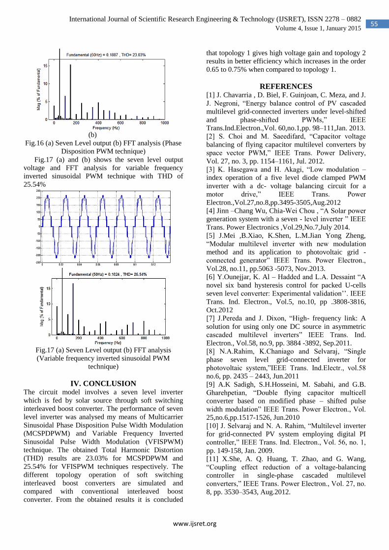
www.ijsret.org
55 International Journal of Scientific Research Engineering & Technology (IJSRET), ISSN 2278 – 0882
Volume 4, Issue 1, January 2015
(b)
Fig.16 (a) Seven Level output (b) FFT analysis (Phase
Disposition PWM technique)
Fig.17 (a) and (b) shows the seven level output
voltage and FFT analysis for variable frequency
inverted sinusoidal PWM technique with THD of
25.54%
Fig.17 (a) Seven Level output (b) FFT analysis
(Variable frequency inverted sinusoidal PWM
technique)
IV. CONCLUSION The circuit model involves a seven level inverter
which is fed by solar source through soft switching
interleaved boost converter. The performance of seven
level inverter was analysed my means of Multicarrier
Sinusoidal Phase Disposition Pulse Width Modulation
(MCSPDPWM) and Variable Frequency Inverted
Sinusoidal Pulse Width Modulation (VFISPWM)
technique. The obtained Total Harmonic Distortion
(THD) results are 23.03% for MCSPDPWM and
25.54% for VFISPWM techniques respectively. The
different topology operation of soft switching
interleaved boost converters are simulated and
compared with conventional interleaved boost
converter. From the obtained results it is concluded
that topology 1 gives high voltage gain and topology 2
results in better efficiency which increases in the order
0.65 to 0.75% when compared to topology 1.
REFERENCES [1] J. Chavarria , D. Biel, F. Guinjoan, C. Meza, and J.
J. Negroni, “Energy balance control of PV cascaded
multilevel grid-connected inverters under level-shifted
and phase-shifted PWMs,” IEEE
Trans.Ind.Electron.,Vol. 60,no.1,pp. 98–111,Jan. 2013.
[2] S. Choi and M. Saeedifard, “Capacitor voltage
balancing of flying capacitor multilevel converters by
space vector PWM,” IEEE Trans. Power Delivery,
Vol. 27, no. 3, pp. 1154–1161, Jul. 2012.
[3] K. Hasegawa and H. Akagi, “Low modulation –
index operation of a five level diode clamped PWM
inverter with a dc- voltage balancing circuit for a
motor drive,” IEEE Trans. Power
Electron.,Vol.27,no.8,pp.3495-3505,Aug.2012
[4] Jinn –Chang Wu, Chia-Wei Chou , “A Solar power
generation system with a seven - level inverter ” IEEE
Trans. Power Electronics ,Vol.29,No.7,July 2014.
[5] J.Mei ,B.Xiao, K.Shen, L.M.Jian Yong Zheng,
“Modular multilevel inverter with new modulation
method and its application to photovoltaic grid -
connected generator” IEEE Trans. Power Electron.,
Vol.28, no.11, pp.5063 -5073, Nov.2013.
[6] Y.Ounejjar, K. Al – Hadded and L.A. Dessaint “A
novel six band hysteresis control for packed U-cells
seven level converter: Experimental validation’’. IEEE
Trans. Ind. Electron., Vol.5, no.10, pp .3808-3816,
Oct.2012
[7] J.Pereda and J. Dixon, “High- frequency link: A
solution for using only one DC source in asymmetric
cascaded multilevel inverters” IEEE Trans. Ind.
Electron., Vol.58, no.9, pp. 3884 -3892, Sep.2011.
[8] N.A.Rahim, K.Chaniago and Selvaraj, “Single
phase seven level grid-connected inverter for
photovoltaic system,”IEEE Trans. Ind.Electr., vol.58
no.6, pp. 2435 – 2443, Jun.2011
[9] A.K Sadigh, S.H.Hosseini, M. Sabahi, and G.B.
Gharehpetian, “Double flying capacitor multicell
converter based on modified phase – shifted pulse
width modulation” IEEE Trans. Power Electron., Vol.
25,no.6,pp.1517-1526, Jun.2010
[10] J. Selvaraj and N. A. Rahim, “Multilevel inverter
for grid-connected PV system employing digital PI
controller,” IEEE Trans. Ind. Electron., Vol. 56, no. 1,
pp. 149-158, Jan. 2009.
[11] X.She, A. Q. Huang, T. Zhao, and G. Wang,
“Coupling effect reduction of a voltage-balancing
controller in single-phase cascaded multilevel
converters,” IEEE Trans. Power Electron., Vol. 27, no.
8, pp. 3530–3543, Aug.2012.
www.ijsret.org
56 International Journal of Scientific Research Engineering & Technology (IJSRET), ISSN 2278 – 0882
Volume 4, Issue 1, January 2015
[12] J.M Shen , H. L. Jou, and J. C. Wu, “Novel
transformer-less grid connected power converter with
negative grounding for photovoltaic generation
system,” IEEE Trans. Power Electron., Vol. 27, no. 4,
pp. 1818 – 1829, Apr. 2012
[13] Sheng –Yu Tseng, Cheng –Tao Tsai,
“Photovoltaic Power System with an Interleaving
Boost Converter for battery charger applications”
International Journal of Photoenergy, Vol. 2012, Sep.
2012.
[14] CH. Shravan, D.Narasimharao, “An Interleaved
Boost Converter with Zero –Voltage Transition for
grid connected PV system” International Journal of
Emerging trends in Engineering and Development,
Vol.2, March 2012.
[15] Thielemans, A. Ruderman, B. Reznikov,
“Improved natural balancing with modified phase-
shifted PWM for single-leg five level flying-capacitor
converters,” IEEE Trans. Power Electron., Vol. 27,no.
4, pp. 1658–1667, Apr. 2012.
[16] S. Vazquez, J. I. Leon, L. G. Franquelo, J. J.
Padilla, and J. M. Carrasco, “DC-voltage-ratio control
strategy for multilevel cascaded converters fed with a
single DC source,” IEEE Trans. Ind. Electron., Vol.
56, no. 7,pp. 2513–2521