Embed Size (px)
Citation preview
Performance Analysis of Sampled Values-Based Protection in IEC 61850 Process Bus
Networks
Nicholas Michael Skoff
Thesis submitted to the faculty of the Virginia Polytechnic Institute and State University in partial fulfillment of the requirements for the degree of
Master of Science In
Electrical Engineering
Jaime De La Ree Lopez, Chair Virgilio A. Centeno Leyla Nazhand-Ali
May 5, 2020 Blacksburg, VA
Keywords: Digital Substations, Sampled Measured Values, Protection Automation, IEC 61850, Process Bus
Performance Analysis of Sampled Values-Based Protection in IEC 61850 Process Bus Networks
Nicholas Skoff
ABSTRACT
As the IEC 61850 digital substation standard becomes progressively
adopted by utilities throughout the world, entirely computerized methods will
completely replace traditional strategies for monitoring the power system.
Although newer techniques offer enhanced efficiency and controllability, their
reliability is not as established as that of conventional practices. Modern
approaches require extensive validation and analysis before they can be
implemented on a widespread basis. One specific area of interest is the
performance of protection systems that utilize voltage and current samples
digitized directly at their source. This research presents a complete test bench for
evaluating sampled values-based protection schemes and measures their efficacy
under several different operating conditions. It is shown that the novel system
operates correctly for the situations it is expected to, with minimal latency
compared to traditional practices.

Performance Analysis of Sampled Values-Based Protection in IEC 61850 Process Bus Networks
Nicholas Skoff
GENERAL AUDIENCE ABSTRACT
Power system infrastructures are changing rapidly from analog
arrangements to entirely digital methods. This offers numerous benefits such as
increased efficiency, lower cost, higher accuracy, and even improved safety.
However, digital implementations do not have an as proven track record as
compared to conventional practices, leading to concerns about their reliability.
This research tests the performance an entirely digital power system protection
scheme by using various hardware components. The results are analyzed and
show that the novel scheme operates correctly, albeit with a slight delay as
compared to traditional methods.

iv
Acknowledgements
First and foremost, I would like to thank my parents Michael and Sharon
Skoff for supporting my education my entire life and pushing me to always be my
best. You are the best role models I could ever hope to have. Additionally, I would
like to thank Dr. Jaime De La Ree for providing me mentorship throughout my
graduate school career and serving as the chair of my committee. Next, I would
like to thank Dr. Virgilio Centeno and Dr. Leyla Nazhand-Ali for their advice on my
research and sitting on my committee. Lastly, I would like to thank Dominion
Energy and Dr. Matthew Gardner for providing the funding of my graduate studies
and fostering this opportunity.
v
Table of Contents
Acknowledgements ........................................................................................... iv
Table of Contents ................................................................................................ v
List of Figures ................................................................................................... vii
1 Introduction .............................................................................................. 1
2 Literature Review ..................................................................................... 4
2.1 Digital Substations ..................................................................................... 5
2.1.1 Process Level Functions and Devices ............................................. 6
2.1.2 Bay Level Functions and Devices ................................................... 7
2.2 IEC 61850 Protocols .................................................................................. 8
2.2.1 Generic Object Oriented Substation Events .................................... 9
2.2.2 Sampled Measured Values ........................................................... 10
2.3 Sampled Values Performance Analysis in Industry .................................. 11
3 Digital Distance Protection Methodology ............................................ 13
3.1 Data Acquisition ....................................................................................... 14
3.1.1 Three Phase Amplifier ................................................................... 15
3.1.2 Analog Filtering ............................................................................. 17
3.1.3 DC Offset ....................................................................................... 21
3.1.4 MSP432E401Y Microprocessor .................................................... 23
3.1.5 Time Synchronization .................................................................... 25
3.2 Process Bus Network ............................................................................... 28
3.2.1 IEC 61850 Packet Configuration ................................................... 29
3.2.2 Latencies in Switched Ethernet Networks ..................................... 31
3.3 Protection IED .......................................................................................... 34
3.3.1 Digital Filtering ............................................................................... 35
3.3.2 Phasor Estimation ......................................................................... 37
3.3.3 Distance Protection of Transmission Lines .................................... 41
3.3.4 Transmission Line Parameters ...................................................... 42
vi
3.3.5 Fault Characteristics ...................................................................... 44
4 Performance Results and Analysis ...................................................... 45
4.1 Sampled Value Simulations ..................................................................... 46
4.1.1 Zero Added Network Traffic ........................................................... 46
4.1.2 Light Network Loading ................................................................... 47
4.1.3 Medium Network Loading .............................................................. 49
4.1.4 Heavy Network Loading ................................................................ 50
4.1.5 Extreme Network Loading ............................................................. 51
4.2 Traditional Relay Comparison .................................................................. 54
4.2.1 Rated Secondary Values ............................................................... 54
4.2.2 Burdened Secondary Values ......................................................... 55
5 Conclusion .............................................................................................. 56
Works Cited ....................................................................................................... 57
Appendix A ........................................................................................................ 59
Appendix B ........................................................................................................ 61
Appendix C ........................................................................................................ 64
vii
List of Figures
Figure 1.1: Simplified Current Transformer Secondary ................................................................................... 2
Figure 1.2: Simplified Potential Transformer Secondary ................................................................................. 3
Figure 2.1: Digital Substation Architecture ....................................................................................................... 5
Figure 3.1: Block Diagram of Test Bench Setup ............................................................................................ 14
Figure 3.2: Omicron CMC 256 Amplifier ........................................................................................................ 15
Figure 3.3: Scaled Secondary Current ........................................................................................................... 16
Figure 3.4: Scaled Secondary Voltage ........................................................................................................... 17
Figure 3.5: 60 Hz Cosine Wave Sampled at 600 Hz ...................................................................................... 18
Figure 3.6: 60 Hz Cosine Wave Sampled at 110 Hz ...................................................................................... 18
Figure 3.7: Filter Magnitude at 60 Hz ............................................................................................................. 20
Figure 3.8: Filter Magnitude at Nyquist Frequency ........................................................................................ 20
Figure 3.9: Filter Phase Shift at 60 Hz ........................................................................................................... 21
Figure 3.10: Input Circuit for Current .............................................................................................................. 22
Figure 3.11: Input Circuit for Voltage ............................................................................................................. 22
Figure 3.12: CPU Timer Controlled Sampling ................................................................................................ 24
Figure 3.13: Cycle Budget for Microprocessor ............................................................................................... 27
Figure 3.14: Switched Ethernet Process Bus ................................................................................................. 28
Figure 3.15: Seven Layer Network Model ...................................................................................................... 28
Figure 3.16: Sampled Value Packet Structure ............................................................................................... 30
Figure 3.17: Digitally Filtered Secondary Current .......................................................................................... 36
Figure 3.18: Digitally Filtered Secondary Voltage .......................................................................................... 36
Figure 3.19: Recursive Phasor Estimation ..................................................................................................... 39
Figure 3.20: Transient Monitoring of Phase A Current ................................................................................... 40
Figure 3.21: Distance Protection Scheme ...................................................................................................... 41
Figure 3.22: Example Transmission Line ....................................................................................................... 43
Figure 4.1: Case 1 Oscilloscope Capture....................................................................................................... 47
Figure 4.2: Case 2 Oscilloscope Capture....................................................................................................... 48
Figure 4.3: Case 3 Oscilloscope Capture....................................................................................................... 50
Figure 4.4: Case 4 Oscilloscope Capture....................................................................................................... 51
Figure 4.5: Corrupted Sampled Data ............................................................................................................. 52
Figure 4.6: Corrupted IA Phasor Magnitude................................................................................................... 53
Figure 4.7: Correct IA Phasor Magnitude ....................................................................................................... 53
Figure 4.8: Protection Response of SEL-421 ................................................................................................. 54
Figure A.1: QuickCMC Menu ......................................................................................................................... 59
Figure A.2: State Sequencer Menu ................................................................................................................ 60
Figure B.1: QuickSet Main Menu ................................................................................................................... 61
Figure B.2: Communication Parameters ........................................................................................................ 62
Figure B.3: Get Event Files ............................................................................................................................ 63
Figure B.4: Available Event Reports .............................................................................................................. 63

1
1 Introduction
As the world moves deeper into the 21st century and an increasingly
technological era, many industries are adopting more and more digital methods in
their everyday operations. One field being drastically impacted by this trend is
power system protection and control. Legacy protection infrastructures make use
of electromechanical relays, devices that detect faults on the power grid using only
continuous forces produced by sensed voltages and currents. The operating
condition of a power system can be determined from the measured voltage and
current. For those cases where the operating point enters a predetermined area,
or cuts through a threshold value a circuit breaker is operated to isolate the
disturbance or abnormal condition. Modern systems take advantage of
microprocessor-based relays to detect if the sensed quantities warrant a trip signal.
Instead of moving physical armatures and coils, the input waveforms are digitized
and fed to an algorithm.
Since there are a variety of different faults possible, it follows suit that a
variety of operating characteristics are necessary to maintain complete coverage.
Unfortunately, since the electromechanical relays are entirely analog, a separate
one is required for each individual function required. Naturally, the number of
devices accumulates rapidly as the power system grows, leading to increased
costs and complexity for the utility. With digital relays, this issue is substantially
alleviated. Several protection functions as well as all three phases can be
implemented in one device thanks to microprocessors. If the relay has enough
2
computing power, digitalization offers a convenient way to consolidate all the
desired qualities in one compact module.
Although the demand for numerous devices is reduced by computer-based
relays, some issues are still present due to the way the input waveforms are
delivered from the substation yard to the control house. Primary power system
quantities are far too large in magnitude to be fed to relays directly so they must
be scaled to safe and manageable levels first. This is achieved via step down
transformers that produce a reduced version of the original signals. The secondary
of these transducers is then fed to the relays in the control house, sometimes
hundreds of feet away. Not only does this represent an enormous cost in terms of
copper wiring, but some of the original signal is lost because of the voltage drop
down the line. Additionally, once the wire reaches its destination it may be input
to several devices, increasing the secondary burden of the transducer.
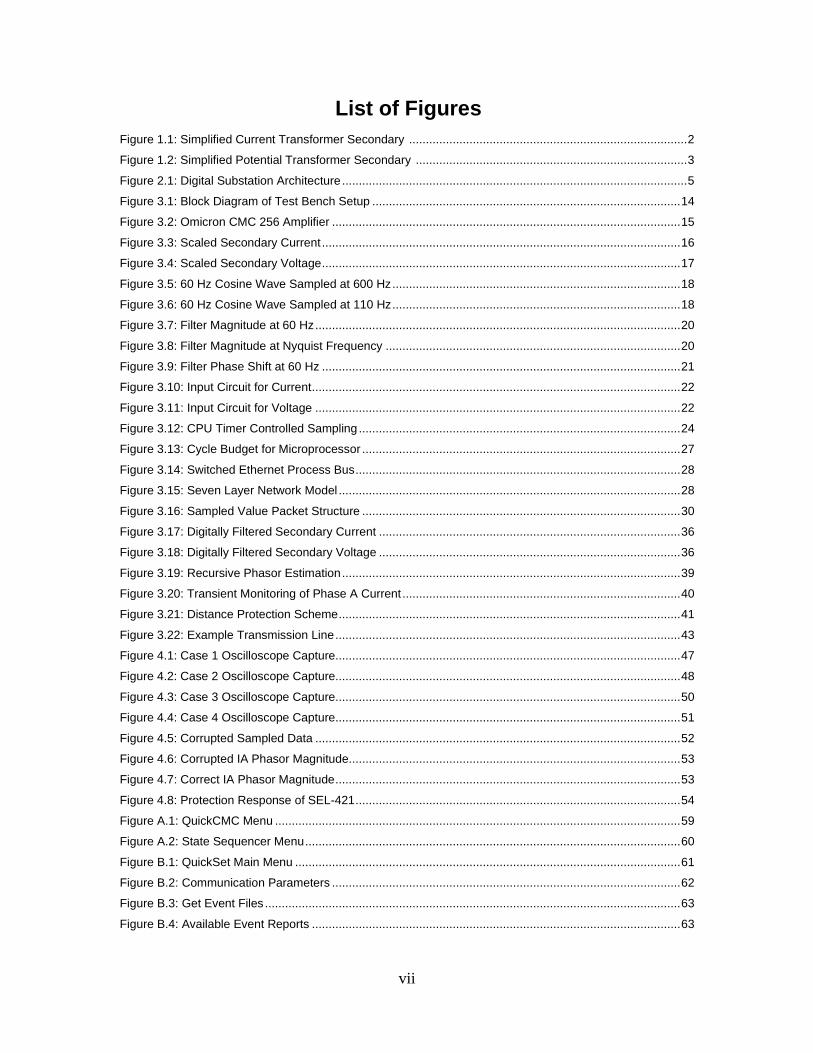
For devices requiring current this means they must be connected in series,
ideally with zero impedance. Connecting more and more components in series
will increase the secondary impedance, as depicted in Figure 1.1. This leads to
inaccuracies in the measured quantity, as well as increases the risk of the current
transformer saturating. Saturation would cause the current to be replicated non-
linearly, further increasing measurement errors.
Figure 1.1 – Simplified Current Transformer Secondary
3
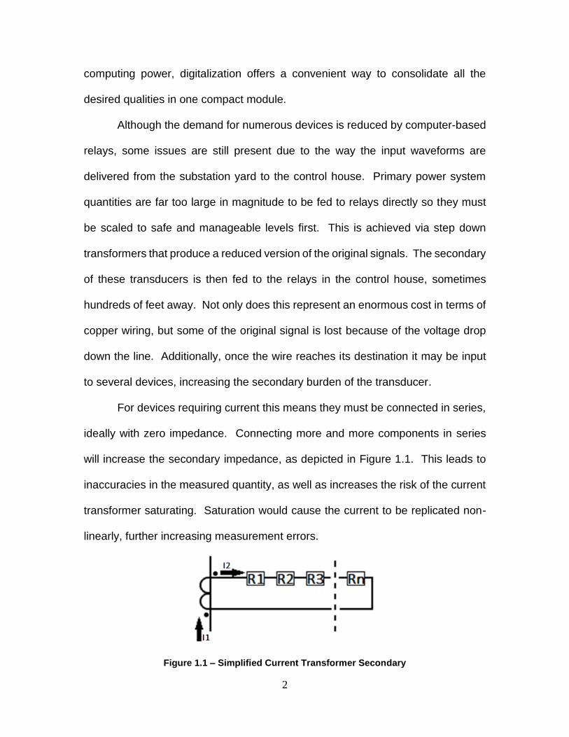
A similar issue exists for the secondaries of potential transformers;
however, the problem is inverted. An ideal voltmeter has infinite impedance so
that it does not dissipate any of the energy from the signal being measured. If
several devices require the same voltage input, they will be connected in parallel.
As more are added in parallel the secondary impedance will drop (Fig. 1.2), and
more of the transduced signal will be lost.
Figure 1.2 – Simplified Potential Transformer Secondary
Since microprocessor relays already use digital values and have
communications abilities, a more efficient method to provide the required signals
is to digitize them immediately after they are stepped down and then send them to
each relay on a high-speed network. A system such as this one places the burden
on the network rather than physical wires, which represents its own set of
challenges such as latency, timing, cybersecurity, and electromagnetic
interference. When designed properly; however, they can perform just as reliably
and even more accurately as compared to conventional protection schemes. This
thesis explores the implementation and performance of a sampled value-based
distance protection scheme for a transmission line, including everything from the
analog secondary signals to the trip signal generated by the relay. Then,
characteristics of the entirely digital system are compared to the same fault
condition applied directly to an SEL-421 distance relay.
4
2 Literature Review
There is extensive documentation on the details of digital substations
including network architecture, standards, and functional requirements. The
primary reference for these types of systems is IEC 61850 [1], an international
standard dictating communication protocols for intelligent electronic devices (IEDs)
used in power grids. The specific features of IEC 61850 implemented in this thesis
as are described in this chapter to familiarize the reader with the concepts
presented. Additionally, a recent study concerning the performance of an IEC
61850 protection scheme is discussed.
2.1 Digital Substations
Power systems are transforming from legacy analog infrastructures to
increasingly digital arrangements, spurred by the invention of microprocessors.
Digital protection relays are widespread, yet they are not always used to their full
capabilities. Typically, these devices’ functionality is limited to just their protection
algorithms, accomplished via copper wire interfaces to yard equipment. Most of
these relays possess the ability to transmit and receive information, provided a
network is in place. Inter-device communication allows for data to be exchanged
rapidly throughout substations, enabling superior monitoring and control of the
system.
Due to the numerous types of devices present in power grids, some level of
organization is required before a communication system can be implemented.
5
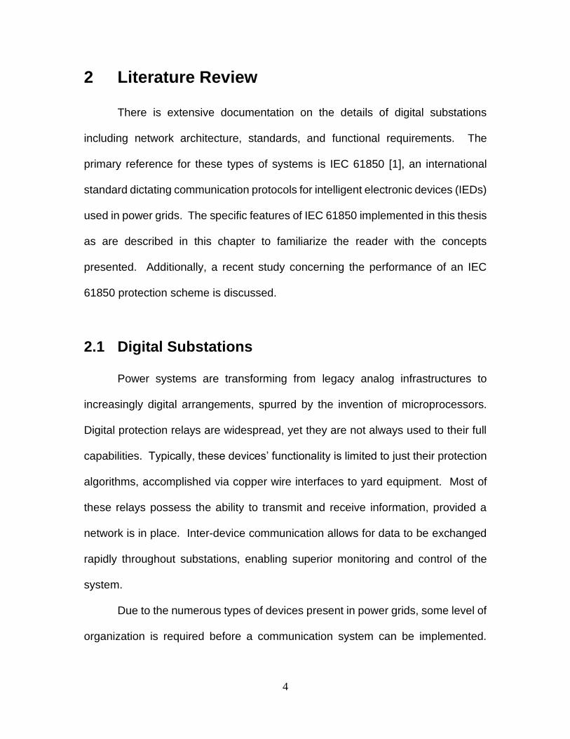
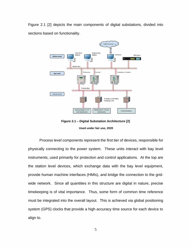
Figure 2.1 [2] depicts the main components of digital substations, divided into
sections based on functionality.
Figure 2.1 – Digital Substation Architecture [2]
Used under fair use, 2020
Process level components represent the first tier of devices, responsible for
physically connecting to the power system. These units interact with bay level
instruments, used primarily for protection and control applications. At the top are
the station level devices, which exchange data with the bay level equipment,
provide human machine interfaces (HMIs), and bridge the connection to the grid-
wide network. Since all quantities in this structure are digital in nature, precise
timekeeping is of vital importance. Thus, some form of common time reference
must be integrated into the overall layout. This is achieved via global positioning
system (GPS) clocks that provide a high accuracy time source for each device to
align to.

6
2.1.1 Process Level Functions and Devices
The process layer forms the physical connection between the actual power
system and the digital abstraction presented above. This includes merging unit
(MU) devices and intelligent circuit breakers. Merging units are responsible for
collecting secondary power system data from either conventional or non-
conventional instrument transformers. Traditional transducers involve magnetic
cores which introduce the risk of saturation and other inaccuracies. When
saturation occurs, the signal on the secondary side of the transformer is no longer
a faithful reproduction of the actual primary quantity. This error can cause
protection systems to behave incorrectly and operate in situations they are not
designed to. Newer types of transformers include optical devices, Rogowski
coils, and power electronics-based converters [4], which can scale down primary
signals without using magnetic cores, thereby eliminating the saturation issue.
Signals must be filtered before being digitized in the merging unit.
Depending on the type of filter put in place, a specific delay will be added to the
measured waveform. Processing these signals and sending them into the system
network introduces another delay as well. When the measured data is being used
for protection purposes, this delay may not exceed 2 ms [5]. Although this amount
of time may not seem significant, it ensures that the performance of the merging
unit is comparable to the traditional method of providing signals to relays.
Since digital substations strive to minimize the copper wire required for the
overall system design, it follows suit that the typical metal wiring between relay
output contacts and circuit breakers is also reduced. Instead, a digital

7
communication link between protection IEDs and switchgear is utilized.
Switchgear control units (SCU) serve this exact purpose, possessing ethernet
ports as well as physical contacts tied directly to the circuit breakers [4]. Trip
signals are received digitally from the protection IEDs and then routed over
conventional wiring to the breaker contacts. To maximize efficiency SCUs are
ideally installed nearby their associated devices; however, subjecting an SCU to
natural elements such as electromagnetic interference, lightning strikes, and other
hostile weather will inevitably increase maintenance requirements. Thus, the
actual implementation of these devices is highly application dependent.
2.1.2 Bay Level Functions and Devices
At this level devices become inherently more complex due to the vital roles
they must serve. Primarily, protection and control related functions are
implemented at this level [4], making use of the data collected by the process
equipment. These types of instruments must respond to changing power system
conditions quickly and act accordingly if it is necessary to sectionalize a portion of
the system. Although process tier devices form the hardwired connection with yard
equipment, bay level instruments possess the actual control over them.
Protective relays for digital substations must demonstrate the same
functionality as their analog counterparts, with increased communication ability.
Their software must be configurable such that they can receive digital quantities
over the process bus, as well as communicate to other devices on the overall
network. This communication could include signals to auxiliary relays, messages
8
with higher level monitoring equipment, and tripping commands to SCUs. Since
these units must interact with both lower and higher-level devices, they must pay
careful attention to the network requirements of both categories [4]. Process bus
communications involve bandwidth intensive streams of power system data, while
bay bus messages are typically more concise.
2.2 IEC 61850 Protocols
A large benefit of IEC 61850 is that it abstracts data independently of the
lower level protocols involved, allowing for station devices to be organized based
on function and then configured quite easily. For example, the standard makes a
distinction between physical and logical components, where several logical
devices may exist within one physical device [3]. Each logical device then may
contain one or several logical nodes, with each node corresponding to a specific
function in the power system. While this is beneficial for organizing the complex
aspects of the standard, the services provided by IEC 61850 must be mapped to
actual protocols for them to be of any use. There are three main mappings in this
standard: Manufacturing Message Specification (MMS), Generic Object Oriented
Substation Events (GOOSE) and Sampled Measured Values (SMV) [3]. This
thesis focuses on the GOOSE and SMV services, which relate heavily to how data
is implemented rather than how it is organized.
9
2.2.1 Generic Object Oriented Substation Events
GOOSE messaging is significantly more prevalent than sampled values-
based communication and thus has a proven track record of reliability in the
electric power industry [4]. As indicated in the name, GOOSE is an event-based
protocol, meaning some change of status must occur for a new type of message
to be sent. Messages indicating the current status of devices, such as circuit
breaker contacts, are continuously transmitted during normal operation [3]. If the
protection system detects a fault on the system and determines that a trip signal
is necessary, this status change gets broadcasted as a continuous burst of
messages that indicate the new configuration [3].
These types of messages present an interesting network design challenge,
since their bandwidth consumption varies depending on the current system
condition. Under steady state operation GOOSE messages do not require very
much bandwidth since they are just intended to confirm a constant state. As soon
as an event occurs, they will congest the network much more since their update
rate increases significantly [6]. To ensure the network is suitable for all types of
system conditions the highest possible bandwidth consumption possible must be
considered. GOOSE messages are mapped directly to ethernet frames where they
can be sent over the process bus network [3]. Their network configuration is
publisher/subscriber based, meaning there is no acknowledgement of received
messages from the subscribing device [3]. This fact is why the message must be
continuously retransmitted at high speeds during events, ensuring delivery of the
updated information.
10
2.2.2 Sampled Measured Values
Sampled values represent digitized secondary currents and voltages that
have been processed by a merging unit and are published on a process bus
network. Unlike GOOSE messages, sampled values are sent at a constant rate
since they must continuously provide information to protection, monitoring, and
control devices. This makes the sampled values extremely bandwidth intensive
for the network. Since the network capabilities will be be constrained mostly by
just the SMV and GOOSE messages, analysis of these two protocols under their
most extreme operation cases is vital to ensure system reliability.
Section 9.1 of IEC 61850 specifies a standardized format for the information
contained in a sampled value packet. This includes three phase measurements
of line voltages, protection currents, metering currents, the bus and neutral voltage,
and two status bits [3]. Using this specified configuration enhances interoperability
between multiple vendors since the data is already in an established format.
Subscriber IEDs need only listen for the incoming messages from the merging unit
and then process it upon its arrival.
Section 9.2 of IEC 61850 offers another interpretation of the sampled value
protocol, offering increased flexibility in how the data is organized. In this version
the data payload is defined by the user, allowing for several different data types
and sizes in the same message [3]. Although this design freedom makes it more
difficult for different vendors to ensure their devices will work properly together,
there is an implementation guideline for section 9.2 that defines a standardized
data set. The conventional three phase voltages and currents are included, as
11
well as status information about the collected data. This includes a sample
counter, a time synchronization bit, and a configuration revision bit [7].
Additionally, the guideline imposes a sampling rate of 80 samples per nominal
power system frequency cycle [7]. Thus, in a 60 Hz system this amounts to 4.8
kHz. Protection IEDs do not typically need this high of a resolution to adequately
perform their functions, however the extra data creates new possibilities for
protection algorithms. For instance, transients can be analyzed in more detail with
the sampling rate offered by IEC 61850, allowing for better fault detection and
classification abilities.
2.3 Sampled Value Performance Analysis in Industry
Due to the requirement that sampled values perform protection and control
functions as reliably as traditional methods, several papers have been published
concerning the implementation of such schemes. One such paper involves the
testing of merging units specifically. The latency between the time of sampling
and publication from the merging unit is measured, amounting to an average of
1050 microseconds [8]. Processing delay accounts for this time difference since
the measured values must be filtered, time-stamped and packaged into ethernet
packets before being published. A subscriber IED receives the sampled value
streams after another specific delay, introduced by the process bus network.
Network latency provides a useful parameter for assessing the performance of
sampled values-based protection schemes in addition to the publication time
measured in [8].
12
A test bench is described in [6] that measures the overall delays in a
sampled values-based protection schemes under different network conditions.
The most important parameters to investigate are bandwidth consumption and
packet loss, since they directly affect the speed of the protection response [6].
Protection IEDs must be able to detect packet loss conditions and respond
appropriately, which will further delay operation under fault scenarios. In this
paper, packets are deleted at a fixed rate rather than dropped due to network
bandwidth constraints. This is not entirely representative of actual systems since
the packets are lost more randomly. Additionally, [6] states that the processing
time of the trip signal between the protection IED and the merging unit accounts
for most of the latency of the digital system.
Alternative network design involving communication of the trip signal to a
switchgear control unit rather than a merging unit may present superior
characteristics since the sole function of the SCU is to control breakers. This trait
inherently reduces the processing time required for the message to be deciphered
and then actuated into a physical disconnection in the power system.
13
3 Digital Distance Protection Methodology
A complete hardware test bench is assembled to simulate each device
involved in a digital protection system. Additionally, conventional protection
validation methods are carried out so the two systems can be compared. The
implementation in this thesis makes use of the following components:
• Omicron CMC 256 3 Phase Amplifier
• Two Texas Instruments MSP432E401YTM Microprocessors
• Digilent PmodGPSTM
• RSR/VT A&D Board
• Velleman USB Oscilloscope
• Copper Wire Connectors
• RC Components
• LF356 Operational Amplifiers
• SEL-421 Distance Relay
• Two CAT6 Ethernet Cables
• Moxa EDS-316 Ethernet Switch
• Dell Optiplex 390 Computer (Protection IED)
These parts were chosen based on a multitude of factors, including
functionality, price, and accessibility. All important aspects of the digital system
are considered, ensuring that the measured performance is an accurate
representation of how a sampled values-based protection scheme would behave.
A high-level diagram of the project setup is given by Fig. 3.1
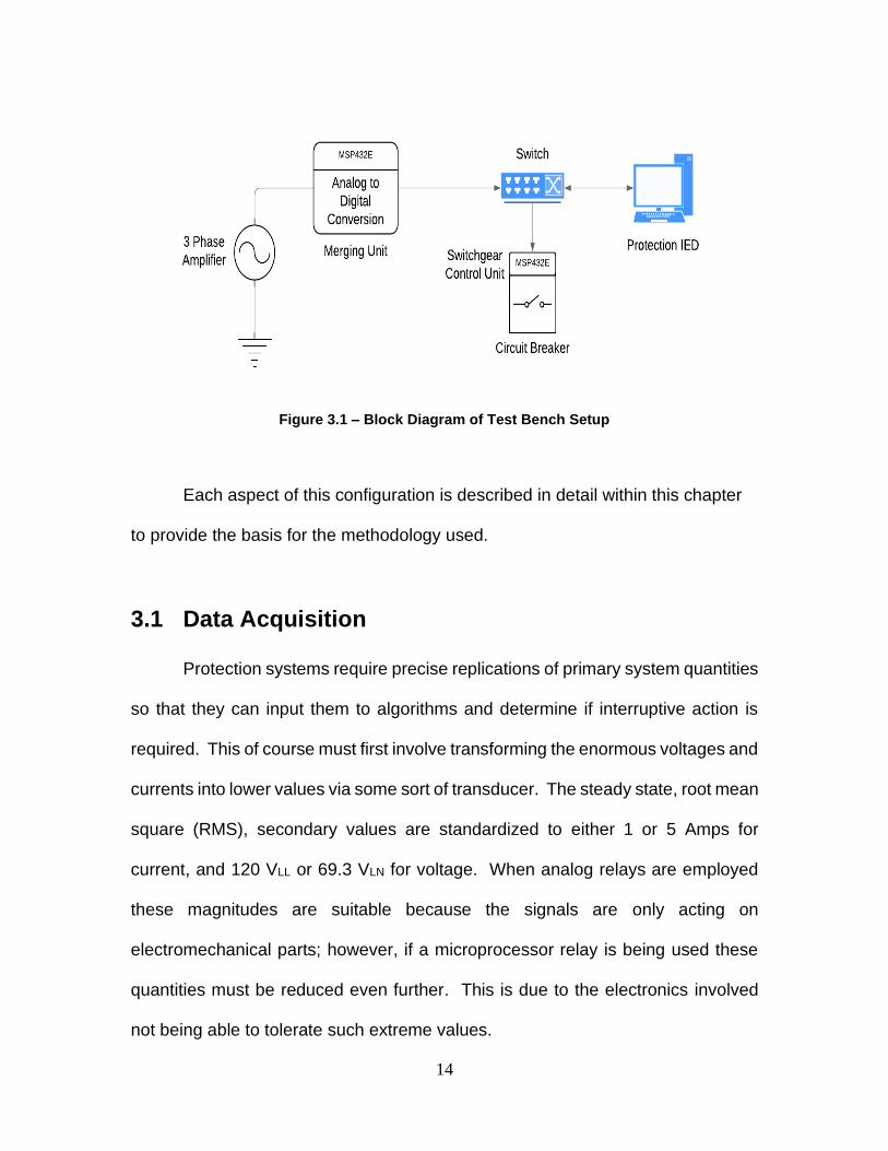
14
Figure 3.1 – Block Diagram of Test Bench Setup
Each aspect of this configuration is described in detail within this chapter
to provide the basis for the methodology used.
3.1 Data Acquisition
Protection systems require precise replications of primary system quantities
so that they can input them to algorithms and determine if interruptive action is
required. This of course must first involve transforming the enormous voltages and
currents into lower values via some sort of transducer. The steady state, root mean
square (RMS), secondary values are standardized to either 1 or 5 Amps for
current, and 120 VLL or 69.3 VLN for voltage. When analog relays are employed
these magnitudes are suitable because the signals are only acting on
electromechanical parts; however, if a microprocessor relay is being used these
quantities must be reduced even further. This is due to the electronics involved
not being able to tolerate such extreme values.
15
3.1.1 Three Phase Amplifier
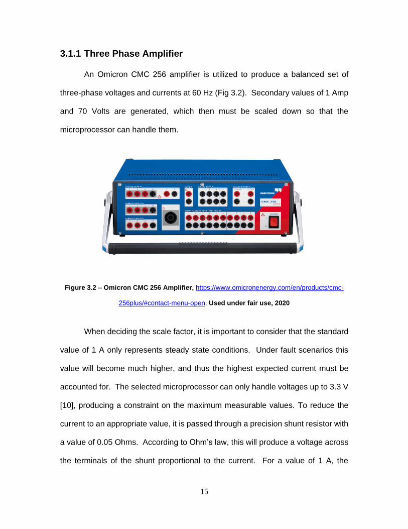
An Omicron CMC 256 amplifier is utilized to produce a balanced set of
three-phase voltages and currents at 60 Hz (Fig 3.2). Secondary values of 1 Amp
and 70 Volts are generated, which then must be scaled down so that the
microprocessor can handle them.
Figure 3.2 – Omicron CMC 256 Amplifier, https://www.omicronenergy.com/en/products/cmc-
256plus/#contact-menu-open, Used under fair use, 2020
When deciding the scale factor, it is important to consider that the standard
value of 1 A only represents steady state conditions. Under fault scenarios this
value will become much higher, and thus the highest expected current must be
accounted for. The selected microprocessor can only handle voltages up to 3.3 V
[10], producing a constraint on the maximum measurable values. To reduce the
current to an appropriate value, it is passed through a precision shunt resistor with
a value of 0.05 Ohms. According to Ohm’s law, this will produce a voltage across
the terminals of the shunt proportional to the current. For a value of 1 A, the
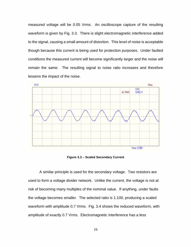
16
measured voltage will be 0.05 Vrms. An oscilloscope capture of the resulting
waveform is given by Fig. 3.3. There is slight electromagnetic interference added
to the signal, causing a small amount of distortion. This level of noise is acceptable
though because this current is being used for protection purposes. Under faulted
conditions the measured current will become significantly larger and the noise will
remain the same. The resulting signal to noise ratio increases and therefore
lessens the impact of the noise.
Figure 3.3 – Scaled Secondary Current
A similar principle is used for the secondary voltage. Two resistors are
used to form a voltage divider network. Unlike the current, the voltage is not at
risk of becoming many multiples of the nominal value. If anything, under faults
the voltage becomes smaller. The selected ratio is 1:100, producing a scaled
waveform with amplitude 0.7 Vrms. Fig. 3.4 shows the reduced waveform, with
amplitude of exactly 0.7 Vrms. Electromagnetic interference has a less
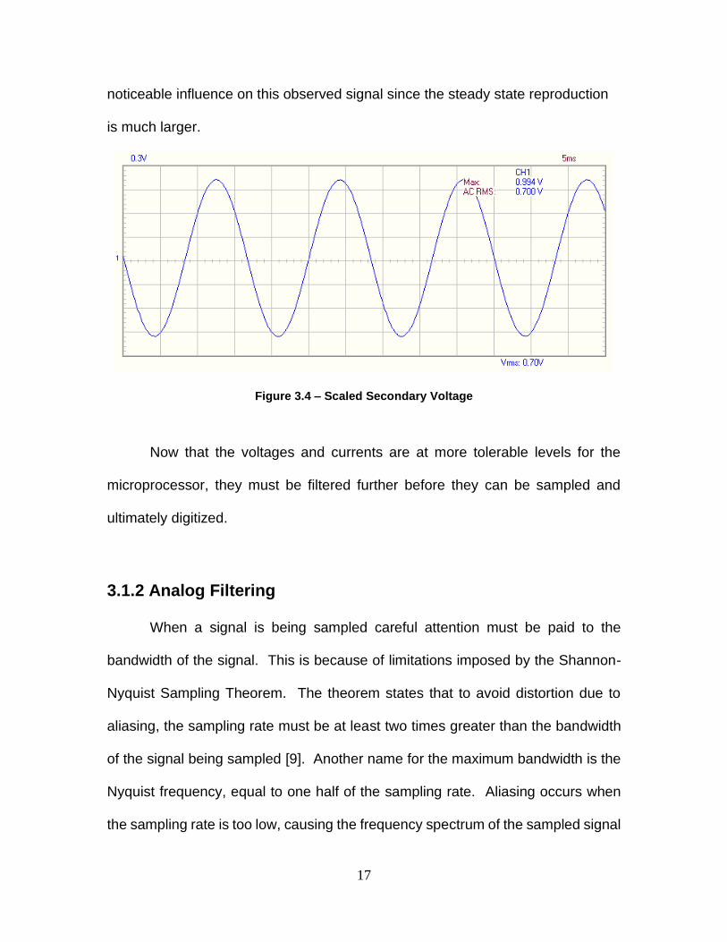
17
noticeable influence on this observed signal since the steady state reproduction
is much larger.
Figure 3.4 – Scaled Secondary Voltage
Now that the voltages and currents are at more tolerable levels for the
microprocessor, they must be filtered further before they can be sampled and
ultimately digitized.
3.1.2 Analog Filtering
When a signal is being sampled careful attention must be paid to the
bandwidth of the signal. This is because of limitations imposed by the Shannon-
Nyquist Sampling Theorem. The theorem states that to avoid distortion due to
aliasing, the sampling rate must be at least two times greater than the bandwidth
of the signal being sampled [9]. Another name for the maximum bandwidth is the
Nyquist frequency, equal to one half of the sampling rate. Aliasing occurs when
the sampling rate is too low, causing the frequency spectrum of the sampled signal
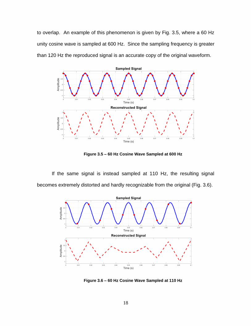
18
to overlap. An example of this phenomenon is given by Fig. 3.5, where a 60 Hz
unity cosine wave is sampled at 600 Hz. Since the sampling frequency is greater
than 120 Hz the reproduced signal is an accurate copy of the original waveform.
Figure 3.5 – 60 Hz Cosine Wave Sampled at 600 Hz
If the same signal is instead sampled at 110 Hz, the resulting signal
becomes extremely distorted and hardly recognizable from the original (Fig. 3.6).
Figure 3.6 – 60 Hz Cosine Wave Sampled at 110 Hz
19
Clearly, aliasing is undesirable as it causes inaccuracies in the perceived
signal. Although increasing the sampling rate helps mitigate this problem, it cannot
be increased indefinitely because it will strain the processor. Additionally, noise
will be present in the signal at frequencies much greater than the fundamental
component. To limit the influence of noise, anti-aliasing filters are used to reject
frequency content after a specified bandwidth.
As mentioned previously, a sampling rate of 4.8 kHz is recommended for
this application. Using this criterion, a low pass filter is designed. Theoretically,
the cutoff frequency could be as large as half of the sampling rate. In practice this
is never done because frequency content slightly higher than 2.4 kHz will only be
minimally attenuated. A good rule of thumb is to have at least 10 dB of reduction
at the Nyquist frequency.
The chosen cutoff frequency for this project is 340 Hz, allowing spectra up
through the 5th harmonic for a 60 Hz signal. This value is selected because it
allows for maximum reduction at the Nyquist frequency, while also minimizing the
phase delay for lower frequencies. Any low pass filter will introduce a phase shift
starting at one tenth of the cutoff frequency, and thus introduce latency into the
system. All digital systems exhibit some sort of delay due to the inherent nature
of sampling. In this instance high speed is of utmost importance because the
sampled values are being used for protection purposes. A simple first order RC
filter is used for simplicity and repeatability because the same input circuit is being
used for each voltage and current channel, resulting in 6 individual filters.
20
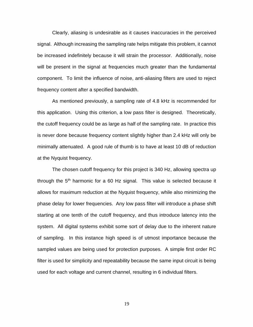
The transfer function of the designed filter is given by Fig. 3.7, showing a
near unity gain at 60 Hz. Even though there is a small reduction at the fundamental
frequency, the gain is constant throughout the pass band and can be easily fixed
via digital filtering. At the Nyquist frequency, the gain is -16.8 dB (Fig. 3.8). This
level of attenuation is quite acceptable and reduces the potential for aliasing to
occur.
Figure 3.7 – Filter Magnitude at 60 Hz
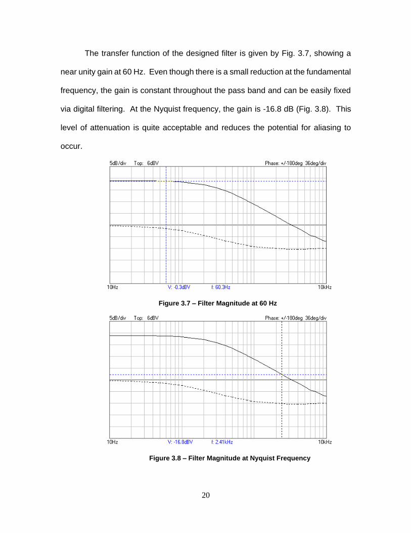
Figure 3.8 – Filter Magnitude at Nyquist Frequency
21
A small phase shift is present at 60 Hz, amounting to -10.7 degrees (Fig.
3.9). This can be digitally corrected for after sampling, however the delay
introduced simply must be dealt with. The delay amounts to 0.495 ms (Eqn. 3.1),
which is tolerable for the presented system.
Figure 3.9 – Filter Phase Shift at 60 Hz
−10.70
3600∗ 16.667 𝑚𝑠 = 0.495 𝑚𝑠
Equation 3.1 – Delay Introduced by Phase Shift
3.1.3 DC Offset
One final step is required before the microprocessor can properly digitize
the waveforms. As mentioned previously, the analog to digital converter on the
MSP432E only tolerates signals between a range of 0 and 3.3 V [10]. Although
the maximum limit was accounted for, these signals are still negative every half
22
cycle and must be given a DC offset. Naturally, the chosen value is 1.65 V
because it will place the alternating signal in the exact middle of the allowable
range. This is achieved with relative ease by using an op-amp adder circuit. A
side benefit offered by this design choice is that the op-amp exhibits a substantial
input impedance. Both secondary waveforms are manifested as small amplitude
voltages, and the high input impedance will ensure that a minimal amount of the
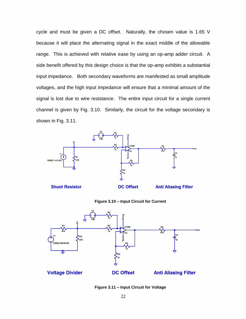
signal is lost due to wire resistance. The entire input circuit for a single current
channel is given by Fig. 3.10. Similarly, the circuit for the voltage secondary is
shown in Fig. 3.11.
Figure 3.10 – Input Circuit for Current
Figure 3.11 – Input Circuit for Voltage

23
3.1.4 MSP432E401Y Microprocessor
Now that the signals are properly conditioned, they can be input to the
microprocessor. The MSP432E401Y features a 12-bit successive approximation
analog to digital converter (ADC), capable of sampling rates up to 2 MHz [10]. This
type of device works by comparing the measured voltage to a certain threshold.
Initially, the compared value is one half of the voltage range. Depending if the
measured signal is smaller or larger than this threshold, the sample is then
compared to either one fourth of the voltage range or three fourths, respectively.
This process is repeated until the value converges and a digital result is obtained.
Since only 12 bits are available to represent the continuous signal, it follows suit
that only a finite resolution is possible. With 12 bits there are 4095 possible values
to discretize a voltage range of 3.3 volts into. An expression for this resolution,
denoted Q, is given by Eqn 3.2.
𝑄 = 3.3 𝑉
212 − 1 = 0.8059 𝑚𝑉
Equation 3.2 – Resolution of ADC
This is the smallest resolvable voltage difference required to generate two
unique discrete quantities, which introduces a small amount of error in the digital
approximation. When the sampled values are being used for metering this level
of inaccuracy may be unacceptable, since extremely precise measurements are
desired for billing purposes. However, when the sampled values are implemented
in protection schemes the slight error is not as significant. To illustrate this, a fault
is considered that produces 10 times the rated secondary current of 1 Amp. For
signals of 10 Amps, the digitized value will exhibit a maximum error of 2.44 mA.

24
This discrepancy is much too small to affect the protection logic; therefore, it is
negligible. If higher accuracy is desired for post fault analysis, the resolution of the
ADC must simply be increased.
The sampling frequency is controlled by a CPU timer that will trigger a start-
of-conversion (SOC) exactly 4800 times each second. A counter is loaded with
the desired sampling period in terms of CPU clock cycles (Fig. 3.12). Using a clock
frequency of 120 MHz, this amounts to 25000 cycles. Whenever the counter is at
a maximum, a SOC is triggered and the ADC will begin converting the voltage it is
receiving. Since there are six individual signals that must be converted, six
separate pins are configured to sample when the SOC flag is generated. Each
conversion will take a certain amount of time, and so the six channels are assigned
priorities to so that an order is established. Once the final sample is converted a
processor interrupt is triggered, and the digital values are read from their
respective registers.
Figure 3.12 – CPU Timer Controlled Sampling
25
3.1.5 Time Synchronization
Digital substations must employ some form of time synchronization or else
the data being exchanged will have virtually no meaning. This is achieved via
global positioning system (GPS) clocks that align devices to a common time
source. Some common methods of GPS synchronization are pulse per second
(PPS), inter-range instrumentation group B (IRIG-B), and precision time protocol
(PTP) [8]. Each offer their own advantages, and thus there is not a universally
standardized procedure for ensuring timing accuracy. In this project, a pulse per
second is utilized via the Pmod GPS. As the name suggests, a pulse is transmitted
once each second with a high degree of precision. This is used to re-align the
sampling clock at the start of each new second. Although the oscillator used in the
MSP432E401Y is highly precise, the crystal may drift over time and cause the
sampling frequency to be slightly off from 4.8 kHz.
At the inception of a new second, a rising edge pulse is transmitted from a
pin on the GPS unit to a pin on the microprocessor. This pulse then triggers a
processor interrupt, which enables the CPU timer to start initiating conversions.
Once the CPU timer is enabled the pulse per second is only required to restart the
process under two separate conditions: ten minutes have passed and the timer
simply needs to realign, or a pulse is not received. In the latter case, a flag is set
indicating the loss of the synchronizing pulse. When the pulse is detected again
the timer will finish its current second and then disable itself. Upon receipt of the
next pulse, the timer begins, and synchronism is maintained.
26
To keep track of time during the second a sample counter is used. The very
first sample is assigned an index of 0, which then increments for each consecutive
sample. Near the end of the second, count 4799 is reached and the counter resets.
Although the sample count can keep track of which fraction of a second the sample
occurred, broader information is required for the complete timestamp. Samples
can be aligned based off the sample count alone, but increased detail is needed
so that phasors calculated from the sampled values can be published in
accordance with IEEE C37.118.1-2011 [11].
A more detailed time tag is provided by the GPS unit through a serial
communication interface. Sentences containing positional data, coordinated
universal time (UTC), and satellite information are delivered from the GPS to the
microprocessor [12]. Unfortunately, serial communication is quite slow compared
to the sampling rate used. The Pmod GPS can be configured to a maximum
transmission speed of 115,200 symbols per second. While this may seem fast, it
is about 100 times slower than the processor clock. Typical sentences are around
65 bytes, which translates to 564 microseconds. For a sampling rate of 4.8 kHz,
there is only 208 microseconds of free processor time to handle additional tasks.
To get around this, only the first 15 bytes are received, and the remainder of the
message is ignored. The only relevant information in the sentence is the UTC
time, which is conveniently at the beginning of the message. Other data, such as
the latitude and longitude, is fixed anyway and can be hard coded into the program
if that information is desired.
27
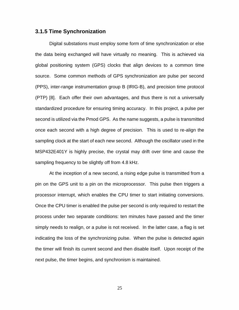
A diagram of the processors’ cycle budget during the first sampling period
is given by Fig. 3.13. As described, the serial message takes up the majority of
the allotted window. Other functions are necessary to read the converted data and
then print it to a string, but they take considerably less time. Nonetheless, all
required operations are completed within 208 microseconds.
Figure 3.13 – Cycle Budget for Microprocessor
Data is formatted into a string containing all voltages, currents, the sample
count, a synchronization flag, and the UTC information. In accordance with IEC
61850 9-2, the data included in this string can be user configurable. For instance,
neutral current and voltage are not included because they can be calculated from
the known quantities. Using a standardized format is beneficial for industry
because it improves interoperability between vendors, but in this implementation it
is not required. After the data is packaged into the desired form, it is ready to be
distributed to the process bus network.
28
3.2 Process Bus Network
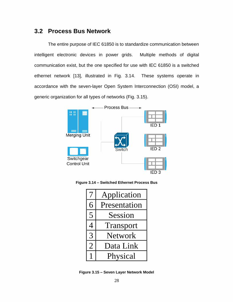
The entire purpose of IEC 61850 is to standardize communication between
intelligent electronic devices in power grids. Multiple methods of digital
communication exist, but the one specified for use with IEC 61850 is a switched
ethernet network [13], illustrated in Fig. 3.14. These systems operate in
accordance with the seven-layer Open System Interconnection (OSI) model, a
generic organization for all types of networks (Fig. 3.15).
Figure 3.14 – Switched Ethernet Process Bus
7 Application
6 Presentation
5 Session
4 Transport
3 Network
2 Data Link
1 Physical
Figure 3.15 – Seven Layer Network Model
29
This model defines each portion of the network in terms of the function it
serves, organized as a stack with the lowest level process at the bottom [14].
When a data payload is sent it is encapsulated at the highest layer and then
wrapped in the descending protocols. At the receiver, the message is then
reconstructed in ascending order. Each layer introduces latency by formatting
certain fields of the ethernet packet.
3.2.1 IEC 61850 Packet Configuration
Due to the time critical nature of Sampled Value and GOOSE messages,
these services are transcribed directly to the data link layer of the ethernet network
stack. This is opposed to traditional transport layer mappings such as User
Datagram Protocol (UDP) and Transmission Control Protocol (TCP). While these
two protocols are useful for more general communication, they add unnecessary
processing delay due to the ethernet frame headers they introduce. The data link
level allows for a packet to be manually constructed using the source and
destination Media Access Control (MAC) address. A MAC address is a unique
identifier for a physical device within the network.
In the case of Sampled Values, the source address simply represents the
merging unit. The destination address is more complicated because multiple
devices may require the information being sent. For this reason, IEC 61850
specifies that Sampled Values must be distributed on the process bus in a
publisher/subscriber-based fashion [13]. This means that several devices can
accept data from a single unit, provided they are configured appropriately. To
30
achieve this, multicast addressing is utilized so that the subscribing IED only needs
to be set to accept data using the specified multicast MAC address. After the the
source and destination addresses, information about the EtherType is inserted.
Sampled Values use a unique identifier of 0x88BA that is only used for this specific
application [7]. This field acts as a header for the data contained in the frame,
identifying what exactly the message will contain.
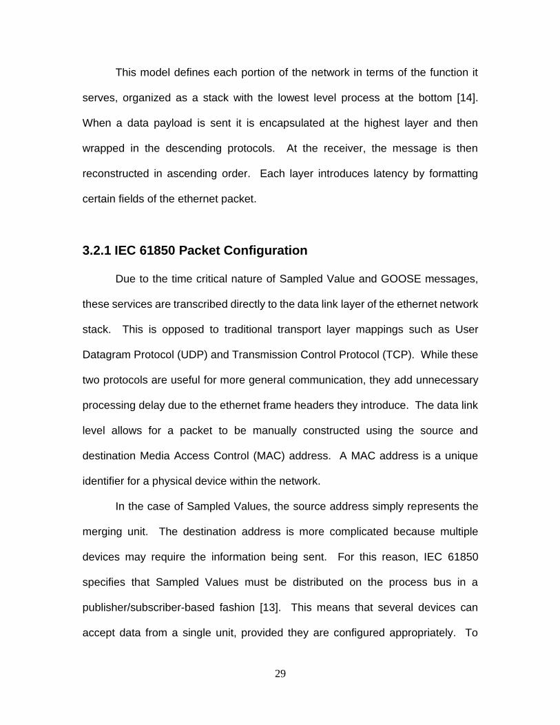
Apart from the addressing and identifier information, the transmitted packet
contains the actual samples collected from the merging unit. In this
implementation, the first field of the data payload is the sample count. Then, a bit
indicating the synchronization status of the merging unit is included. Next, the
instantaneous values of current for each phase are written, followed by the
voltages. Lastly, for sample count 0 the current UTC time is appended at the end
of the message. Since the resolution of the time data is only one second, it is not
required to continuously be sent. Additionally, increasing the packet length will
cause the message to occupy more bandwidth and strain the network. Bandwidth
plays an important role in network latency, which is discussed in the following
section. The overall packet structure for sampled values used in this thesis is
given by Fig. 3.16.
Figure 3.16 – Sampled Value Packet Structure
31
GOOSE messages are configured in a similar way, but the source address
now belongs to the protection IED. The EtherType for these types of packets is
0x88BB [3], indicating that the data payload will contain binary substation status
information. In this application the only attribute to monitor is the circuit breaker
contact. Under normal conditions, the GOOSE message is broadcasted once
each second to indicate that the contacts are closed. If the protection algorithm
determines that the breaker must open a burst of messages is then sent to indicate
the new status, signifying a trip signal [6]. Upon receipt of the trip message, the
switchgear control unit outputs a physical voltage to the circuit breaker contacts.
To mimic the functionality of the SCU, another MSP432E401Y is used to detect
the GOOSE message and provide the corresponding output.
3.2.2 Latencies in Switched Ethernet Networks
The performance of both Sampled Value and GOOSE messages is of
utmost concern, since the correct operation of the power system is dependent on
their reliable and timely delivery. There are several sources of latency in switched
ethernet networks, each contributing to the overall performance [15]. Components
of network delay explored in this thesis are as follows:
• Frame Transmission delay
• Queuing delay
• Protocol latency
• Operating system delay
32
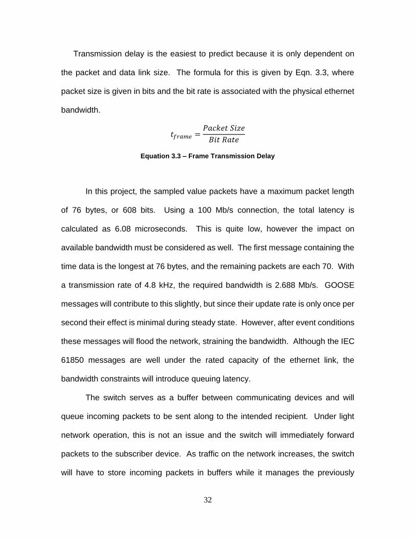
Transmission delay is the easiest to predict because it is only dependent on
the packet and data link size. The formula for this is given by Eqn. 3.3, where
packet size is given in bits and the bit rate is associated with the physical ethernet
bandwidth.
𝑡𝑓𝑟𝑎𝑚𝑒 =𝑃𝑎𝑐𝑘𝑒𝑡 𝑆𝑖𝑧𝑒
𝐵𝑖𝑡 𝑅𝑎𝑡𝑒
Equation 3.3 – Frame Transmission Delay
In this project, the sampled value packets have a maximum packet length
of 76 bytes, or 608 bits. Using a 100 Mb/s connection, the total latency is
calculated as 6.08 microseconds. This is quite low, however the impact on
available bandwidth must be considered as well. The first message containing the
time data is the longest at 76 bytes, and the remaining packets are each 70. With
a transmission rate of 4.8 kHz, the required bandwidth is 2.688 Mb/s. GOOSE
messages will contribute to this slightly, but since their update rate is only once per
second their effect is minimal during steady state. However, after event conditions
these messages will flood the network, straining the bandwidth. Although the IEC
61850 messages are well under the rated capacity of the ethernet link, the
bandwidth constraints will introduce queuing latency.
The switch serves as a buffer between communicating devices and will
queue incoming packets to be sent along to the intended recipient. Under light
network operation, this is not an issue and the switch will immediately forward
packets to the subscriber device. As traffic on the network increases, the switch
will have to store incoming packets in buffers while it manages the previously
33
received messages. When the network is heavily loaded, this can severely affect
performance so the effect on the protection response is significant. Queueing
latency is difficult to calculate in practice, so it must be measured.
As mentioned previously, typical transport layer protocols like UDP and TCP
are avoided because they introduce unnecessary latency. One aspect of protocol
specific latency is the transmission of acknowledgement packets. In TCP, if a
packet fails to reach its’ destination the sending node will resend the packet until it
receives confirmation that the subscriber received it. This is detrimental for real
time communication applications because new data must be sent at a constant
rate. Due to this, Sampled Value and GOOSE messages send packets with no
bias toward successful delivery. While this is necessary for this application, it
introduces the fact that some messages may be dropped. The protection IED must
be able to detect this condition and act accordingly, since the loss of data may
cause an abnormal response.
The last type of delay investigated in this thesis is operating system latency.
This phenomenon occurs in real time operating systems and stems from interrupt
handling by the processor. Network functions that send the actual packet may
block other portions of code if buffers start to fill up. If this occurs synchronized
sampling may be lost, and the measured data will be heavily corrupted. Like
queuing delay, this effect occurs when the bandwidth limits are being constrained.
Typically, network congestion is not severe enough to observe this effect but the
possibility of the scenario warrants investigation.

34
3.3 Protection IED
The protection relay performs the core functions related to ensuring the
power system remains operational under adverse conditions. In the past, these
devices were entirely analog, but now most protection schemes make use of
microprocessor-based relays. Analog relays measure secondary voltages and
currents and then use electromechanical forces to determine if the values fit within
a certain operating characteristic. The same principle is present within digital
relays; however, they make use of calculated phasors instead of physical
quantities. Consider the sinusoid (Eqn. 3.4) that describes a phase A to neutral
voltage.
𝑣(𝑡) = 𝑉𝐴𝑐𝑜𝑠(𝜔𝑡 + 𝜑)
Equation 3.4 – Phase A Voltage: Sinusoidal Form
There are three parameters that identify this waveform; the magnitude,
frequency, and phase angle. In complex exponential notation, the equation is
written as Eqn. 3.5.
𝑣(𝑡) = 𝑅𝑒[{𝑒𝑗(𝜔𝑡)}𝑉𝐴𝑒𝑗𝜑]
Equation 3.5 – Phase A Voltage: Complex Exponential Form
For power systems the angular frequency is assumed to be constant,
causing a vector of magnitude VA and angle 𝜑 to rotate around a complex plane.
This angular frequency is 377 rad/s in North America, representing the ideal 60 Hz
operating frequency of the power system.

35
Phasors are typically represented by capital, boldface letters (Eqn. 3.6),
representing the complex vector of known magnitude and angle. Additionally, the
magnitude is often reduced by a factor of √2 to represent the RMS value of the
original waveform.
𝑽 = 𝑉𝐴
√𝟐∠ 𝜑
Equation 3.6 – Phase A Voltage: Phasor Form
Digital relays calculate phasors and then input them to algorithms that
determine if interruptive action is necessary. A benefit of microprocessor relays is
that advanced protection schemes are achieved with greater ease due to the
computational power of the processor. For instance, consider the positive,
negative, and zero sequence components that represent a three-phase set under
unbalanced conditions. Electromechanical relays use complex filters to obtain
these quantities, while computer relays simply multiply the calculated phasors by
a rotation matrix. Sequence components offer tremendous advantages in
protective relaying because they are only present in large magnitudes during fault
conditions. Of course, the reliability of more complicated schemes or even any
phasor-based algorithm is dependent on the accuracy of the calculated phasor.
3.3.1 Digital Filtering
Before the received samples can be used they must be filtered such that
they represent the actual time domain waveforms. As mentioned in section 3.1.2,
phase and gain offsets occur due to the anti-aliasing filter present in the input
circuit. Additionally, the DC value added to the signals must be removed. A 5 Amp
36
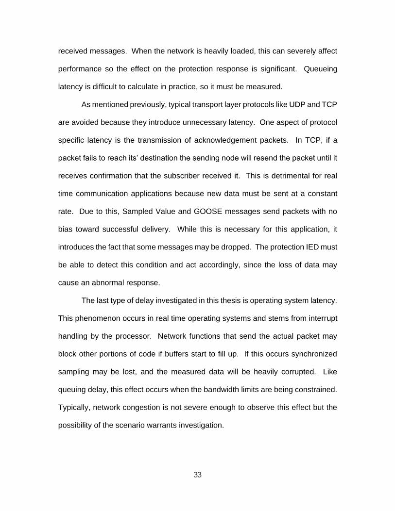
RMS secondary is used to calibrate the current digital filter and the samples are
adjusted accordingly. A time domain plot of the conditioned currents is given by
Fig. 3.17. Similarly, a 70 Volt signal is applied for the voltages and the waveforms
are plotted in Fig. 3.18. In this form, the sampled values are now ready to be input
to phasor estimation methods.
Figure 3.17 – Digitally Filtered Secondary Current
Figure 3.18 – Digitally Filtered Secondary Voltage

37
3.3.2 Phasor Estimation
A variety of techniques exist for calculating phasors from instantaneous
samples for waveforms but they all stem from the same underlying mathematical
concept, the discrete Fourier Transform (DFT) [16]. The DFT works by summing
a finite window of K samples each multiplied by a complex exponential, and then
averaging the result over the duration of the window (Eqn. 3.7). Lowercase k
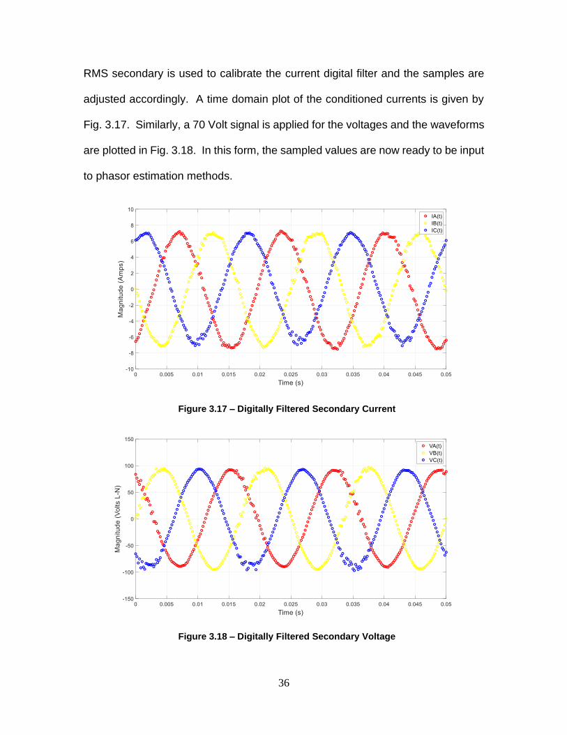
represents the sample index within the window.
𝑽 = 2
𝐾∑ 𝑣(𝑘)𝑒−𝑗
2𝜋𝑘𝐾
𝐾−1
0
Equation 3.7 – Discrete Fourier Transform
A window size of one cycle is selected for simplicity, but other lengths can
be chosen. A longer window yields a more accurate result at the expense of a
lengthier time required to compute the phasor. Conversely, a shorter window
provides an estimate much quicker, but accuracy may suffer. Protection devices
must grapple with this tradeoff since they require faithful representations of the
actual quantities, while also needing to operate as quickly as possible. In this
implementation, a one cycle window is selected since it only requires 16.67 ms
and still provides reliable results.
Since this algorithm is being implemented on a microprocessor, it must be
split into real and imaginary components using Euler’s Formula (Eqn. 3.8). Then,
the magnitude and angle are calculated by converting the results back into polar
form (Eqn 3.9).
38
α = 𝑅𝑒{𝑽} =2
𝐾∑ 𝑣(𝑘)𝑐𝑜𝑠 (
2𝜋𝑘
𝐾)
𝐾−1
0
β = 𝐼𝑚{𝑽} = −2
𝐾∑ 𝑣(𝑘)𝑠𝑖𝑛 (
2𝜋𝑘
𝐾)
𝐾−1
0
Equation 3.8 – Real and Imaginary Decomposition
|𝑽| = √𝛼2 + 𝛽2
∠𝑽 = −𝑡𝑎𝑛−1 (𝛽
𝛼)
Equation 3.8 – Real and Imaginary Decomposition
While these samples shown in Figs. 3.17 and 3.18 are now acceptable to
use in the DFT, each sample within the one cycle window is not required. Although
80 samples per cycle provides quality resolution for post-fault oscillography or
even operational transient analysis, this amount of data points is unnecessary for
protection purposes. This inevitably slows down the time in between when the
samples are received and when the phasor is published. Therefore, the protection
IED down-samples the signals before calculating the phasor. Since the incoming
number of data points is fixed, the resolution of the data window is user
configurable. In this application 8 samples per cycle are used for estimating the
phasor, yielding a reasonable accuracy. With higher speed processors, finer
resolutions can be used and enable the use of even more advanced transient-
based protection algorithms.
39
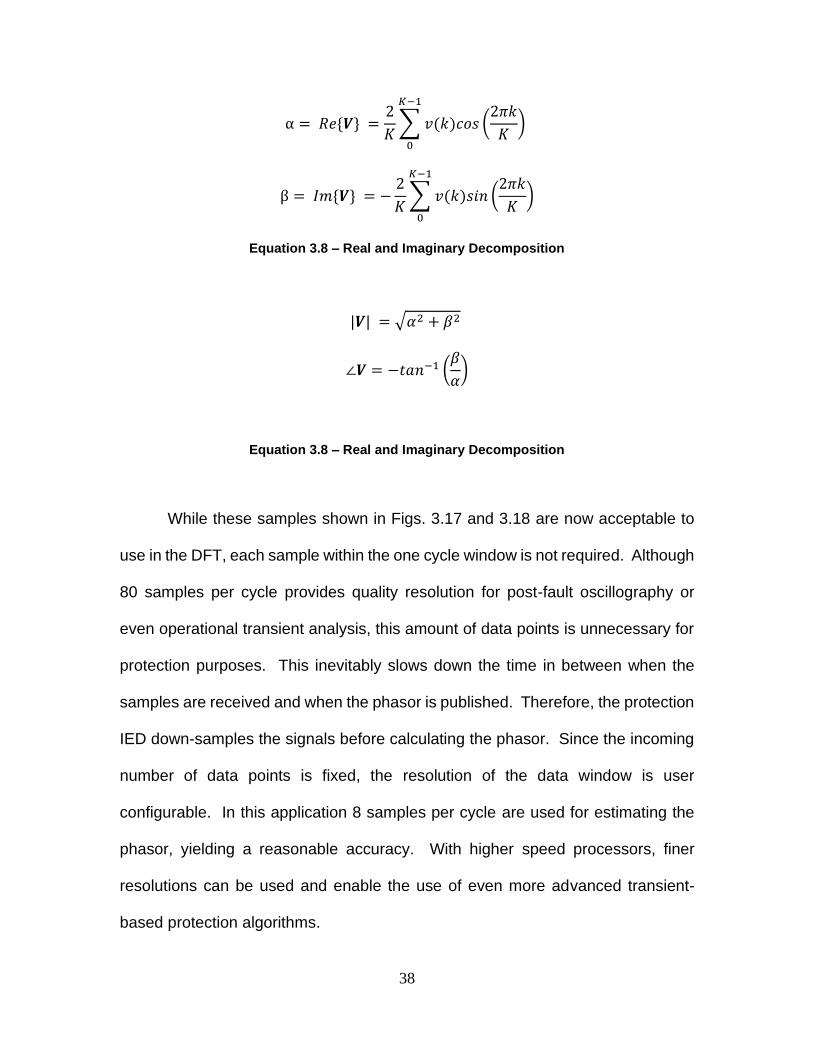
Since the phasors are being used for protection, they must be updated as
quickly as possible. If the one cycle window is used, it may seem like phasors are
only calculated once every 16.67 ms. One cycle’s worth of data is indeed required,
but the starting point of the window is not fixed. After the first phasor of each
second is computed, the next window simply shifts up by one sample point (Fig.
3.19).
Figure 3.19 – Recursive Phasor Estimation
Each new window subtracts the oldest point from the previously calculated
phasor and then adds the newest encapsulated one. This is known as recursive
phasor estimation [16]. In this project, the down-sampling rate is set to 8 ms, so
phasors are published every 2.08 ms. The UTC time data sent each second is
attached to each phasor, along with the fractional second corresponding to the last
sample in the window. This complies with IEEE C37.118.1-2011 [11], which
dictates how synchronized phasor measurements must be taken in power
systems.
A system is now in place to compute phasors from sampled values, but
measures must be taken to ensure that the calculated phasor is accurate. During
transient conditions, the voltages and currents will not be a constant wave for the
40
duration of one cycle. Due to this, there is technically no appropriate phasor to
describe the present signal. After transients die out, the system reaches steady
state again and phasors can be reliably estimated. Therefore, phasors must only
be published during steady conditions.
This is accomplished via transient monitoring [17]. Once a phasor is
calculated, the samples used are compared to an actual sinusoid with magnitude
and phasor consistent with the established value. The magnitude of the difference
between the sample and the “ideal” wave is taken and the compared to a certain
threshold. If the threshold is violated, the phasor is determined to be an unfaithful
measurement, and the value is not used for anything else. This concept is
demonstrated in Fig. 3.19, where the difference between the measured and
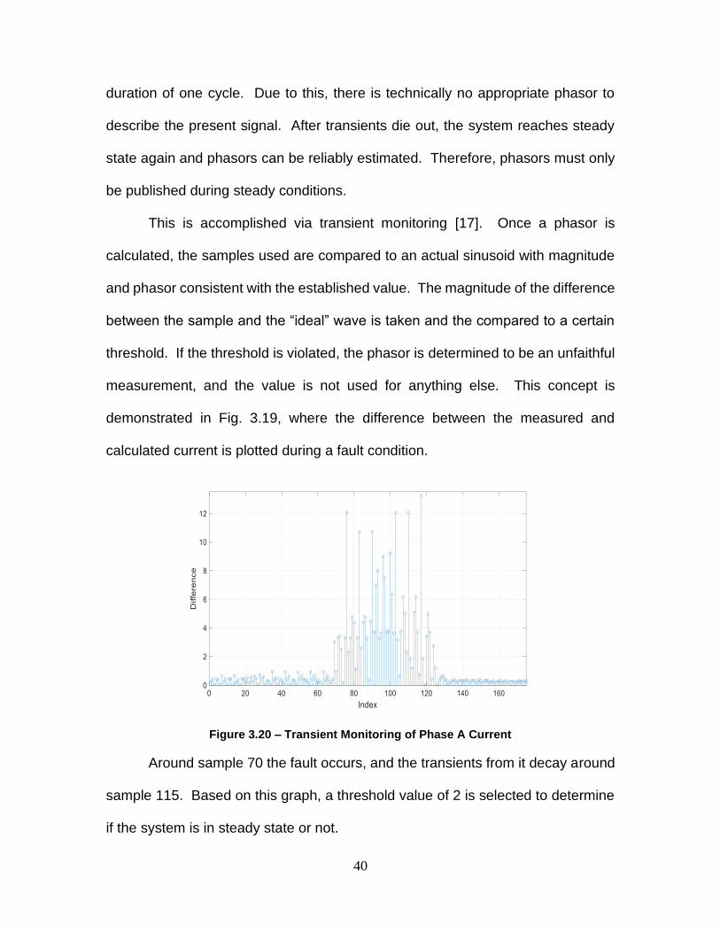
calculated current is plotted during a fault condition.
Figure 3.20 – Transient Monitoring of Phase A Current
Around sample 70 the fault occurs, and the transients from it decay around
sample 115. Based on this graph, a threshold value of 2 is selected to determine
if the system is in steady state or not.
41
3.3.3 Distance Protection of Transmission Lines
With phasors available for all voltages and currents, protection algorithms
can now be implemented. The scheme of interest in this thesis is distance
protection, used to provide coverage for high voltage transmission lines. This
method plots the measured ratio between the voltage and current phasors to
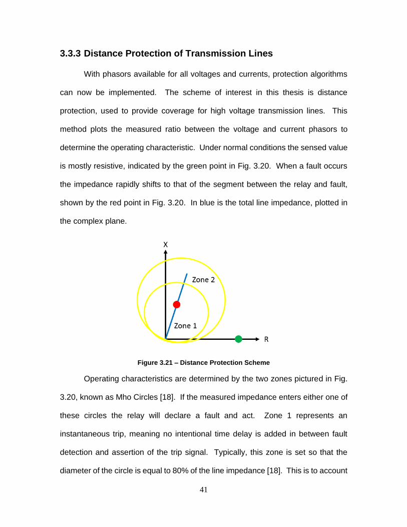
determine the operating characteristic. Under normal conditions the sensed value
is mostly resistive, indicated by the green point in Fig. 3.20. When a fault occurs
the impedance rapidly shifts to that of the segment between the relay and fault,
shown by the red point in Fig. 3.20. In blue is the total line impedance, plotted in
the complex plane.
Figure 3.21 – Distance Protection Scheme
Operating characteristics are determined by the two zones pictured in Fig.
3.20, known as Mho Circles [18]. If the measured impedance enters either one of
these circles the relay will declare a fault and act. Zone 1 represents an
instantaneous trip, meaning no intentional time delay is added in between fault
detection and assertion of the trip signal. Typically, this zone is set so that the
diameter of the circle is equal to 80% of the line impedance [18]. This is to account
42
for uncertainties in the true impedance of the transmission line. If zone 1 were set
to cover the entire line, a bus fault at the remote terminal could cause the local
relay to trip incorrectly for an out of zone fault. To protect the remaining portion of
the line zone 2 is set to 120% of the total impedance [18], but with a time delay
before tripping is initiated.
The delay allows time for zone 1 of the adjacent line to operate first if
necessary. If the fault is beyond the remote terminal, that line’s relay should detect
it and declare an instantaneous trip. Conversely, if the fault is on the actual line
for which the settings are designed for, zone 2 will still assert and issue a trip signal.
This careful balance of delay between separate relays is known as coordination
and must be considered for protection applications requiring overlapping zones,
such as distance schemes.
3.3.4 Transmission Line Parameters
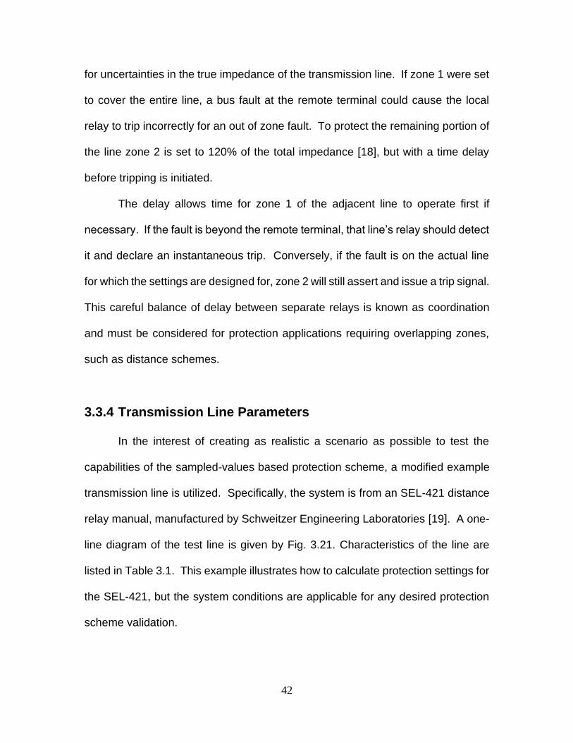
In the interest of creating as realistic a scenario as possible to test the
capabilities of the sampled-values based protection scheme, a modified example
transmission line is utilized. Specifically, the system is from an SEL-421 distance
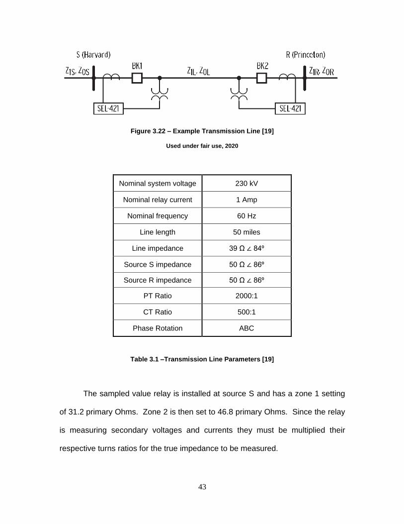
relay manual, manufactured by Schweitzer Engineering Laboratories [19]. A one-
line diagram of the test line is given by Fig. 3.21. Characteristics of the line are
listed in Table 3.1. This example illustrates how to calculate protection settings for
the SEL-421, but the system conditions are applicable for any desired protection
scheme validation.
43
Figure 3.22 – Example Transmission Line [19]
Used under fair use, 2020
Nominal system voltage 230 kV
Nominal relay current 1 Amp
Nominal frequency 60 Hz
Line length 50 miles
Line impedance 39 Ω ∠ 84⁰
Source S impedance 50 Ω ∠ 86⁰
Source R impedance 50 Ω ∠ 86⁰
PT Ratio 2000:1
CT Ratio 500:1
Phase Rotation ABC
Table 3.1 –Transmission Line Parameters [19]
The sampled value relay is installed at source S and has a zone 1 setting
of 31.2 primary Ohms. Zone 2 is then set to 46.8 primary Ohms. Since the relay
is measuring secondary voltages and currents they must be multiplied their
respective turns ratios for the true impedance to be measured.
44
3.3.5 Fault Characteristics
The most common fault within power systems is single line to ground (SLG),
therefore this is the type used for the protection simulation. A SLG fault is taken
on phase A at 20% of the example line. It is assumed that the fault impedance is
0 Ohms, meaning the measured ratio of voltage and current should be exactly 20%
of the overall line impedance. Steady state values of 1 Amp and 70 Volts are
programmed to be output on each phase for 500 ms. After this first half-second
the phase A current output is changed to 10 Amps, while phase B and C reduce
to 0. For the voltage, the measured phase A quantity becomes 19.5 V, and the
remaining phases remain at 70 V. Since it is assumed current is only flowing
through the faulted phase, no voltage drop occurs on the healthy phases. After
multiplying the two phase A quantities by their turn ratios and then calculating the
measured impedance the result yields a fault impedance of 7.8 Ohms, exactly 20%
of the total line. The fault persists for 500 ms, after which the amplifier is turned
off and the simulation is concluded.
When the process bus network is lightly loaded, there should not be a
significant effect on the protection system. As network traffic is increased
performance may degrade. Exactly how significantly performance is affected and
why is the principle investigation of this thesis. To compare the effect of network
burden with traditional secondary burdens, the same voltages and currents are
applied to an SEL-421 at rated value, and at a specified error tolerance.
45
4 Performance Results and Analysis
The reliability of sampled values-based protection schemes under different
network operating conditions is of chief concern, since the communication
infrastructure is the backbone of digital substations. Five test cases are proposed
to test the performance of the protection device.
• No extra network traffic
• 1 Mbps additional traffic
• 2.5 Mbps additional traffic
• 5 Mbps additional traffic
• 25 Mbps additional traffic
These five scenarios represent varying network conditions from entirely
unloaded to completely congested. Packets are injected into the network using
Packet Sender, an open source application for sending network messages to
specified addresses. Since all devices on the process bus share the same switch,
the packets must simply be sent to any other device on the network and they will
affect the bandwidth. Although the Packet Sender utility is a useful tool for testing
networks, it does have certain limitations. The occupied bandwidth within the
network is not perfectly constant and varies by about 1 kbps in either direction of
the specified value. This level of error is acceptable however since the packets’
purpose of straining the network is still achieved.
46
4.1 Sampled Values Simulations
The five test cases described previously are now carried out with five trials
per case. Operating latency is measured by measuring the phase A current and
output tripping signal on an oscilloscope. Fault inception is easily observed as the
point where the current instantly changes direction, and the trip assertion is simply
a rising edge pulse.
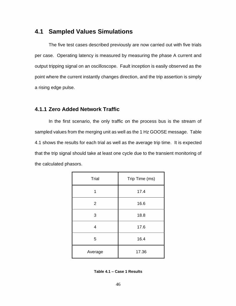
4.1.1 Zero Added Network Traffic
In the first scenario, the only traffic on the process bus is the stream of
sampled values from the merging unit as well as the 1 Hz GOOSE message. Table
4.1 shows the results for each trial as well as the average trip time. It is expected
that the trip signal should take at least one cycle due to the transient monitoring of
the calculated phasors.
Trial Trip Time (ms)
1 17.4
2 16.6
3 18.8
4 17.6
5 16.4
Average 17.36
Table 4.1 – Case 1 Results
47
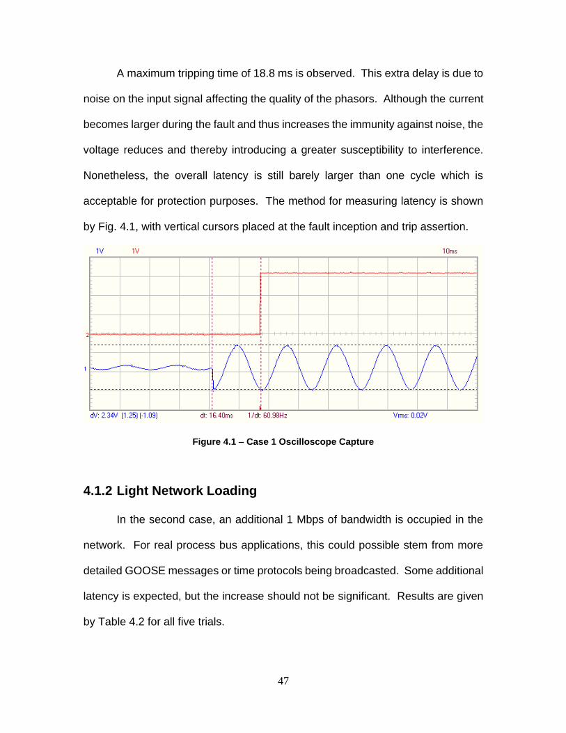
A maximum tripping time of 18.8 ms is observed. This extra delay is due to
noise on the input signal affecting the quality of the phasors. Although the current
becomes larger during the fault and thus increases the immunity against noise, the
voltage reduces and thereby introducing a greater susceptibility to interference.
Nonetheless, the overall latency is still barely larger than one cycle which is
acceptable for protection purposes. The method for measuring latency is shown
by Fig. 4.1, with vertical cursors placed at the fault inception and trip assertion.
Figure 4.1 – Case 1 Oscilloscope Capture
4.1.2 Light Network Loading
In the second case, an additional 1 Mbps of bandwidth is occupied in the
network. For real process bus applications, this could possible stem from more
detailed GOOSE messages or time protocols being broadcasted. Some additional
latency is expected, but the increase should not be significant. Results are given
by Table 4.2 for all five trials.
48
Trial Trip Time (ms)
1 17.2
2 17.6
3 19.2
4 17.6
5 18.0
Average 17.92
Table 4.2 – Case 2 Results
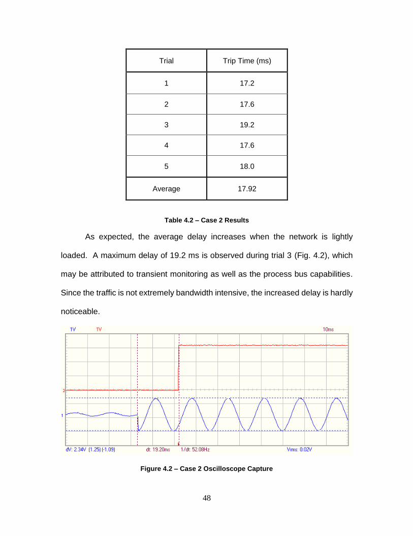
As expected, the average delay increases when the network is lightly
loaded. A maximum delay of 19.2 ms is observed during trial 3 (Fig. 4.2), which
may be attributed to transient monitoring as well as the process bus capabilities.
Since the traffic is not extremely bandwidth intensive, the increased delay is hardly
noticeable.
Figure 4.2 – Case 2 Oscilloscope Capture
49
4.1.3 Medium Network Loading
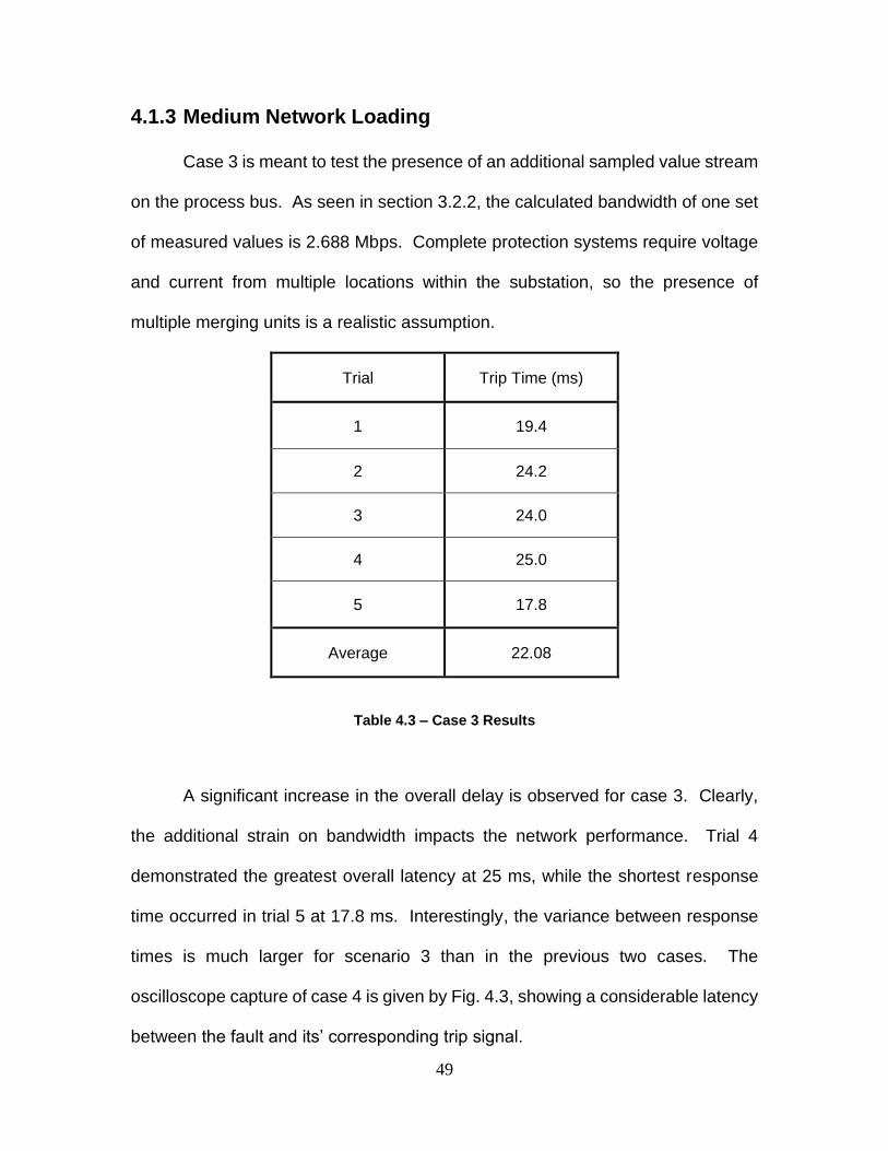
Case 3 is meant to test the presence of an additional sampled value stream
on the process bus. As seen in section 3.2.2, the calculated bandwidth of one set
of measured values is 2.688 Mbps. Complete protection systems require voltage
and current from multiple locations within the substation, so the presence of
multiple merging units is a realistic assumption.
Trial Trip Time (ms)
1 19.4
2 24.2
3 24.0
4 25.0
5 17.8
Average 22.08
Table 4.3 – Case 3 Results
A significant increase in the overall delay is observed for case 3. Clearly,
the additional strain on bandwidth impacts the network performance. Trial 4
demonstrated the greatest overall latency at 25 ms, while the shortest response
time occurred in trial 5 at 17.8 ms. Interestingly, the variance between response
times is much larger for scenario 3 than in the previous two cases. The
oscilloscope capture of case 4 is given by Fig. 4.3, showing a considerable latency
between the fault and its’ corresponding trip signal.
50
Figure 4.3 – Case 3 Oscilloscope Capture
4.1.4 Heavy Network Loading
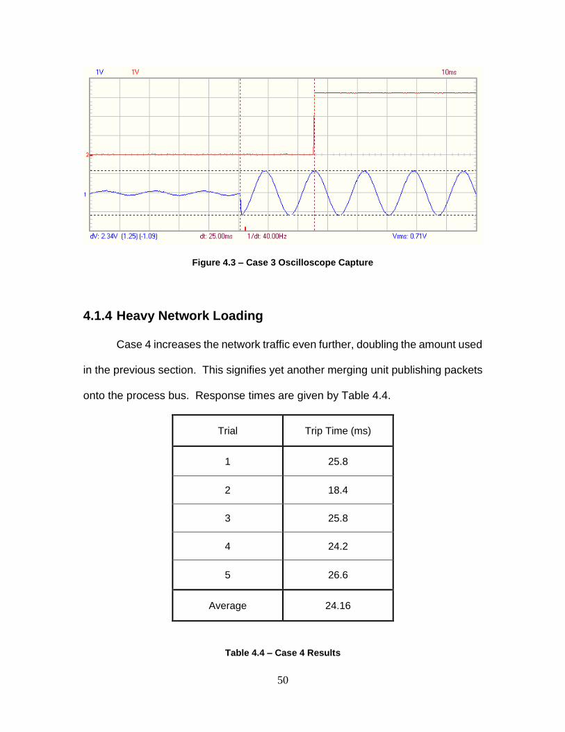
Case 4 increases the network traffic even further, doubling the amount used
in the previous section. This signifies yet another merging unit publishing packets
onto the process bus. Response times are given by Table 4.4.
Trial Trip Time (ms)
1 25.8
2 18.4
3 25.8
4 24.2
5 26.6
Average 24.16
Table 4.4 – Case 4 Results
51
Once again, latency increases as network traffic consumes more of the
available bandwidth. Performance degrades, but the longest response observed
(Fig. 4.4) is still fast enough for most protection applications.
Figure 4.4 – Case 4 Oscilloscope Capture
4.1.5 Extreme Network Loading
The last scenario involves an intense supply of messages being broadcast
onto the network. An additional 25 Mbps of bandwidth is consumed by flooding
the network with traffic. In this case it is observed that the trip signal does not
assert, warranting further investigation within the protection device. Since the
switchgear control unit does not detect any trip signal, the issue is determined to
be with the protection algorithm. It is already seen that the code is functional for
the previous cases, so the problem lies with the data being used to calculate the
phasors. Network traffic is generated and received samples are plotted (Fig. 4.5).
While the result appears sinusoidal, the samples are no longer occurring at a
uniform rate.
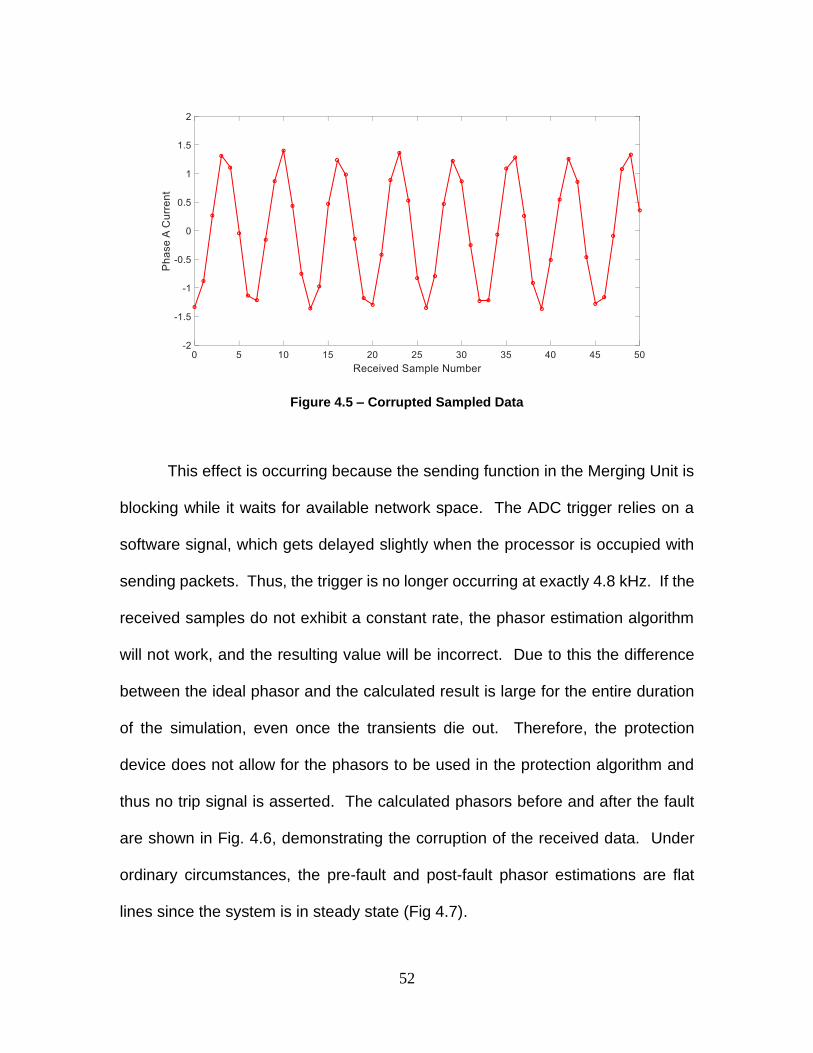
52
Figure 4.5 – Corrupted Sampled Data
This effect is occurring because the sending function in the Merging Unit is
blocking while it waits for available network space. The ADC trigger relies on a
software signal, which gets delayed slightly when the processor is occupied with
sending packets. Thus, the trigger is no longer occurring at exactly 4.8 kHz. If the
received samples do not exhibit a constant rate, the phasor estimation algorithm
will not work, and the resulting value will be incorrect. Due to this the difference
between the ideal phasor and the calculated result is large for the entire duration
of the simulation, even once the transients die out. Therefore, the protection
device does not allow for the phasors to be used in the protection algorithm and
thus no trip signal is asserted. The calculated phasors before and after the fault
are shown in Fig. 4.6, demonstrating the corruption of the received data. Under
ordinary circumstances, the pre-fault and post-fault phasor estimations are flat
lines since the system is in steady state (Fig 4.7).
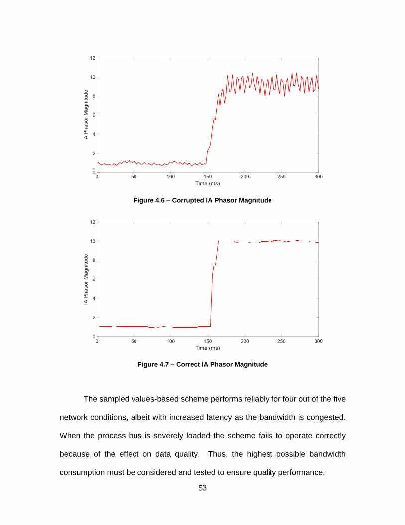
53
Figure 4.6 – Corrupted IA Phasor Magnitude
Figure 4.7 – Correct IA Phasor Magnitude
The sampled values-based scheme performs reliably for four out of the five
network conditions, albeit with increased latency as the bandwidth is congested.
When the process bus is severely loaded the scheme fails to operate correctly
because of the effect on data quality. Thus, the highest possible bandwidth
consumption must be considered and tested to ensure quality performance.
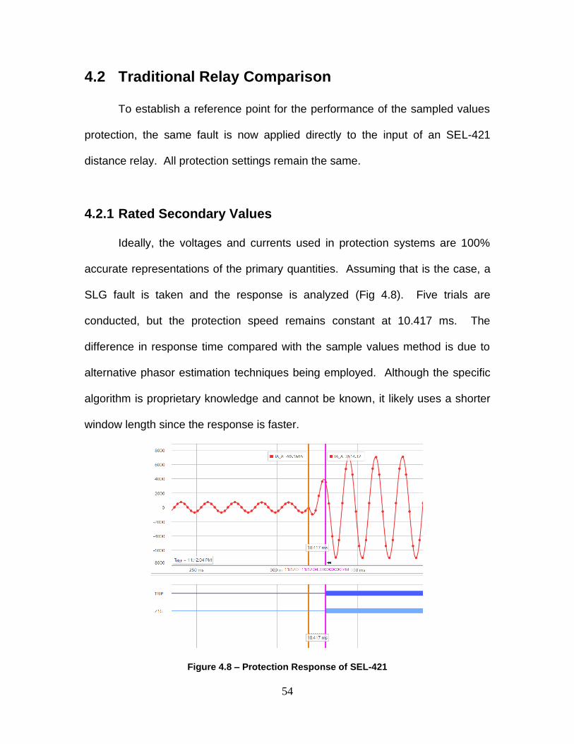
54
4.2 Traditional Relay Comparison
To establish a reference point for the performance of the sampled values
protection, the same fault is now applied directly to the input of an SEL-421
distance relay. All protection settings remain the same.
4.2.1 Rated Secondary Values
Ideally, the voltages and currents used in protection systems are 100%
accurate representations of the primary quantities. Assuming that is the case, a
SLG fault is taken and the response is analyzed (Fig 4.8). Five trials are
conducted, but the protection speed remains constant at 10.417 ms. The
difference in response time compared with the sample values method is due to
alternative phasor estimation techniques being employed. Although the specific
algorithm is proprietary knowledge and cannot be known, it likely uses a shorter
window length since the response is faster.
Figure 4.8 – Protection Response of SEL-421
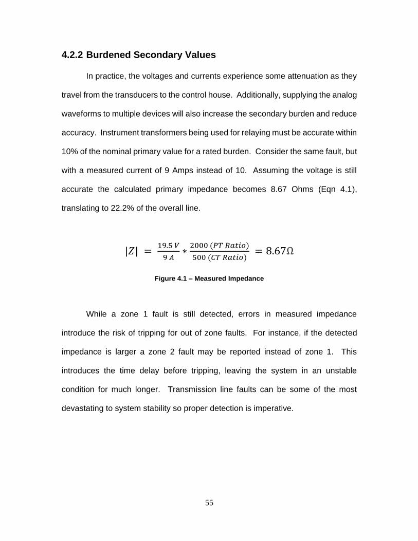
55
4.2.2 Burdened Secondary Values
In practice, the voltages and currents experience some attenuation as they
travel from the transducers to the control house. Additionally, supplying the analog
waveforms to multiple devices will also increase the secondary burden and reduce
accuracy. Instrument transformers being used for relaying must be accurate within
10% of the nominal primary value for a rated burden. Consider the same fault, but
with a measured current of 9 Amps instead of 10. Assuming the voltage is still
accurate the calculated primary impedance becomes 8.67 Ohms (Eqn 4.1),
translating to 22.2% of the overall line.
|𝑍| = 19.5 𝑉
9 𝐴∗
2000 (𝑃𝑇 𝑅𝑎𝑡𝑖𝑜)
500 (𝐶𝑇 𝑅𝑎𝑡𝑖𝑜) = 8.67Ω
Figure 4.1 – Measured Impedance
While a zone 1 fault is still detected, errors in measured impedance
introduce the risk of tripping for out of zone faults. For instance, if the detected
impedance is larger a zone 2 fault may be reported instead of zone 1. This
introduces the time delay before tripping, leaving the system in an unstable
condition for much longer. Transmission line faults can be some of the most
devastating to system stability so proper detection is imperative.
56
5 Conclusion
A complete sampled values-based distance protection scheme is
implemented, and the observed performance is shown to be comparable to
traditional methods. Even under heavy network loading the maximum latency is
26.6 ms, with no expense to accuracy. When network congestion is extremely
high the sampled value scheme fails to operate, but this is expected since this
process bus is not designed for such intense bandwidth consumption. Careful
planning must be taken in digital substations so that this situation never occurs.
Additionally, real applications should use dedicated processors with higher
computing power to ensure that all real-time constraints are met.
Applying the fault directly yields a response time of 10.417 ms, but as
demonstrated, secondary burdens will introduce errors in the measured signal.
This error may be tolerable but the risk of operating incorrectly is inherently
increased. Protection systems ensure the reliable operation of the electric grid,
and thus their performance is of absolute importance. As IEC 61850 becomes
more common in power systems around the world, sampled values-based
schemes will inevitably become the standard method for detecting and isolating
faults. Thus, they must be tested extensively so that they can be depended on in
the same way as conventional protection architectures.
57
Works Cited
[1] IEC TC57, IEC 61850: Communication networks and systems for power
utility automation, International Electro technical Commission Std.
[2] S. McFadyen, “Steven McFadyen,” myElectrical, 02-Mar-2014. [Online].
Available: https://myelectrical.com/notes/entryid/245/how-a-digital-
substation-works. [Accessed: 08-Jan-2020].
[3] R. E. Mackiewicz, "Overview of IEC 61850 and benefits," 2006 IEEE Power
Engineering Society General Meeting, Montreal, Que., 2006, pp. 8 pp.-.
[4] H. Vardhan, R. Ramlachan, W. Szela and E. Gdowik, "Deploying digital
substations: Experience with a digital substation pilot in North
America," 2018 71st Annual Conference for Protective Relay Engineers
(CPRE), College Station, TX, 2018, pp. 1-9.
[5] IEC 61869-9, Instrument Transformers – Part 9: Digital Interface for
Instrument Transformers, 2016.
[6] S. Chase, E. Jessup, M. Silveira, J. Dong, and Q. Yang, “Protection and
testing considerations for IEC 61850 sampled values-based distance and
line current differential schemes”, 72rd Annual Conference for Protective
Relay Engineers, 2019.
[7] UCA International Users Group, “Implementation Guideline for Digital
Interface to Instrument Transformers Using IEC 61850-9-2,” July 2004.
Available: http://iec61850.ucaiug.org/Implementation%20Guidelines/
DigIF_spec_9-2LE_R2-1_040707-CB.pdf.
[8] Q. Yang, D. Keckalo, D. Dolezilek, and E. Cenzon, “Testing IEC 61850
Merging Units”, 44th Annual Western Protective Relay Conference, 2017.
[9] A. Grami, Introduction to digital communications. Amsterdam: Elsevier,
2015.
[10] Texas Instruments Inc., MSP432E401Y SimpleLink™ Ethernet
Microcontroller, 2017
58
[11] IEEE Standard for Synchrophasor Measurements for Power Systems,"
in IEEE Std C37.118.1-2011 (Revision of IEEE Std C37.118-2005) , vol.,
no., pp.1-61, 28 Dec. 2011
[12] D. DePriest, “NMEA data,” GPS Information. [Online]. Available:
https://www.gpsinformation.org/dale/nmea.htm#RMC. [Accessed: 11-Oct-
2019].
[13] I. Ali, M. S. Thomas and S. Gupta, "Sampled values packet loss impact on
IEC 61850 distance relay performance," 2013 IEEE Innovative Smart Grid
Technologies-Asia (ISGT Asia), Bangalore, 2013, pp. 1-6.
[14] Briscoe, N. (2000). Understanding the OSI 7-Layer Model. PC Network
Advisor, 120 (July 2000), 13–14.
[15] Loeser, J. & Haertig, H.. (2004). Low-latency hard real-time communication
over switched Ethernet. 16. 13 - 22. 10.1109/EMRTS.2004.1310992.
[16] A. G. Phadke and J. S. Thorp, Synchronized phasor measurements and
their applications. New York, NY: Springer, 2010.
[17] A. J. Schmitt, “A digital implementation of power system metering and
protection,” Master’s thesis, Virginia Polytechnic Institute and State
University, 2014.
[18] S. H. Horowitz and A. G. Phadke, Power system relaying. Chichester
(England): John Wiley and Sons Ltd, 2014.
[19] SEL-421 Relay Protection and Automation System Applications Handbook,
Schweitzer Engineering Laboratories, Pullman, WA, USA, 2013, p. 41

59
Appendix A
The amplifier used in this research is covered in this section. Steady state
operation as well as fault emulation is described.
A.1 Steady State Testing
Launch the Test Universe software, located in the same carrying case as the
Omicron CMC 256 amplifier. Select the QuickCMC option from the main menu. The
window shown by Fig. A.1 will appear. Fixed values for voltage and current are input into
the red box, with selectable magnitude and phase. To run the simulation, select the red
button outlined by the green box (Fig. A.1).
Figure A.1 – QuickCMC Menu
A.2 Fault Testing
To simulate faults, select the State Sequencer option from the main menu of Test
Universe. The voltages and currents are input like the steady-state case, but now for a
specified time duration (Fig. A.2). In the example, rated secondary values are applied for
500 ms. Then, a phase A to ground fault is taken at t = 500 ms. Instantly, the voltages
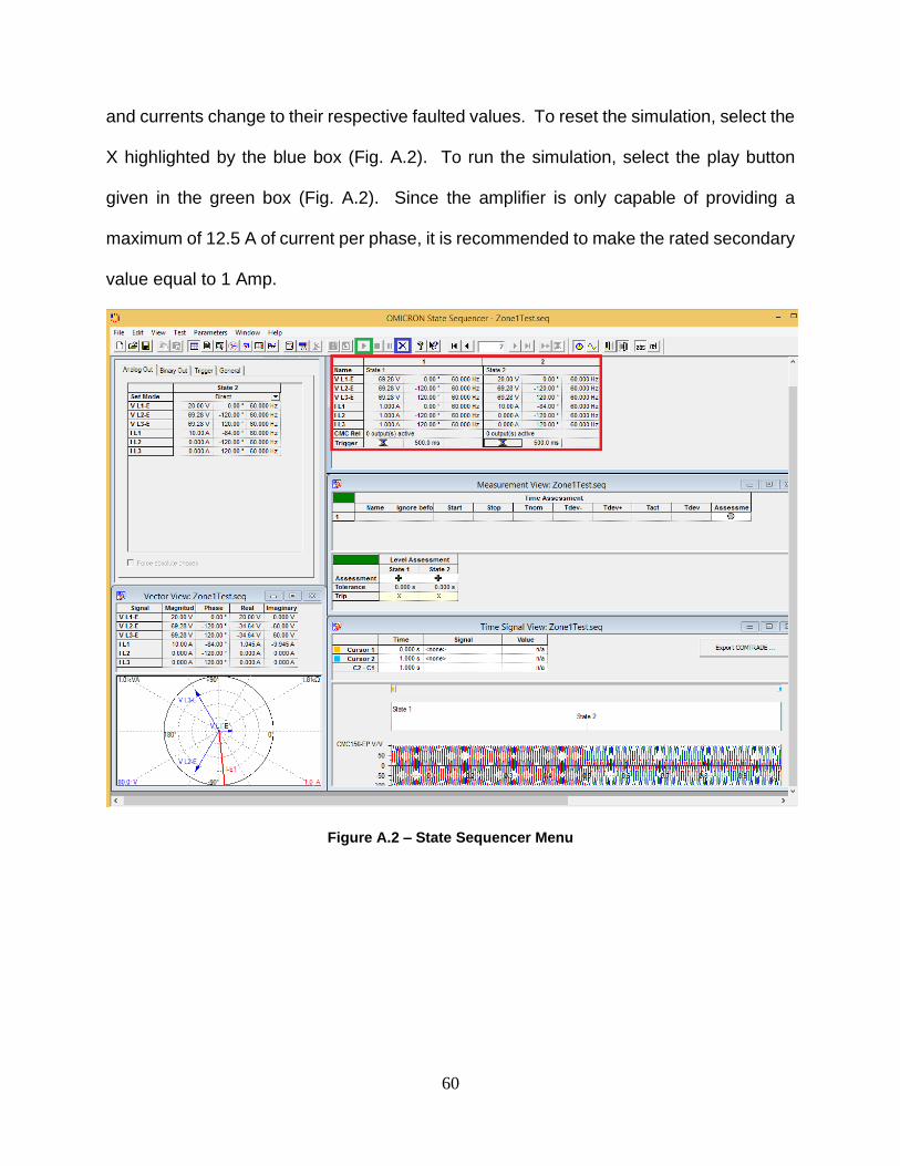
60
and currents change to their respective faulted values. To reset the simulation, select the
X highlighted by the blue box (Fig. A.2). To run the simulation, select the play button
given in the green box (Fig. A.2). Since the amplifier is only capable of providing a
maximum of 12.5 A of current per phase, it is recommended to make the rated secondary
value equal to 1 Amp.
Figure A.2 – State Sequencer Menu
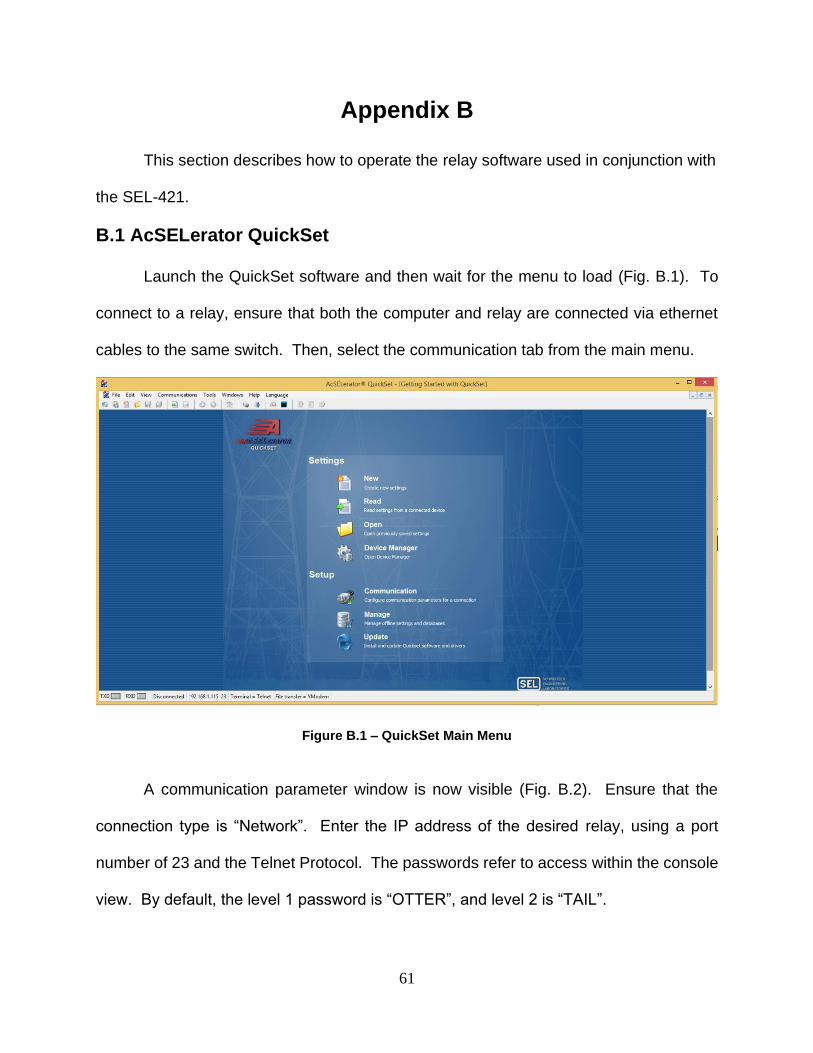
61
Appendix B
This section describes how to operate the relay software used in conjunction with
the SEL-421.
B.1 AcSELerator QuickSet
Launch the QuickSet software and then wait for the menu to load (Fig. B.1). To
connect to a relay, ensure that both the computer and relay are connected via ethernet
cables to the same switch. Then, select the communication tab from the main menu.
Figure B.1 – QuickSet Main Menu
A communication parameter window is now visible (Fig. B.2). Ensure that the
connection type is “Network”. Enter the IP address of the desired relay, using a port
number of 23 and the Telnet Protocol. The passwords refer to access within the console
view. By default, the level 1 password is “OTTER”, and level 2 is “TAIL”.
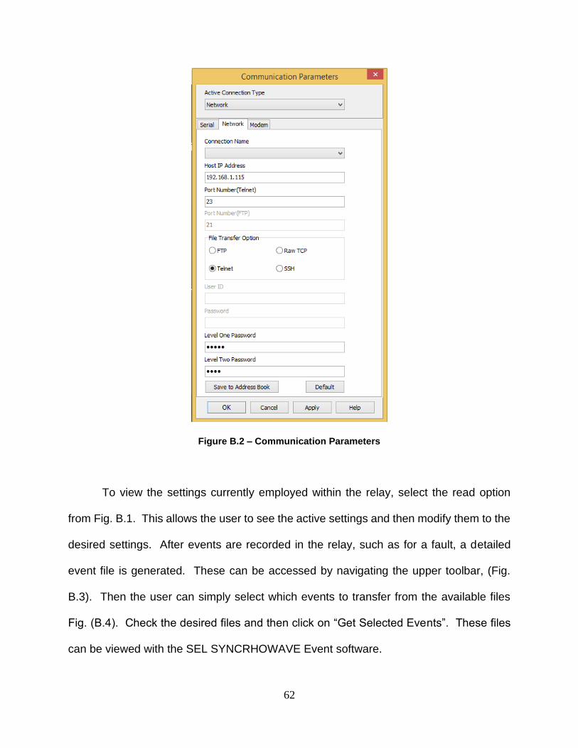
62
Figure B.2 – Communication Parameters
To view the settings currently employed within the relay, select the read option
from Fig. B.1. This allows the user to see the active settings and then modify them to the
desired settings. After events are recorded in the relay, such as for a fault, a detailed
event file is generated. These can be accessed by navigating the upper toolbar, (Fig.
B.3). Then the user can simply select which events to transfer from the available files
Fig. (B.4). Check the desired files and then click on “Get Selected Events”. These files
can be viewed with the SEL SYNCRHOWAVE Event software.
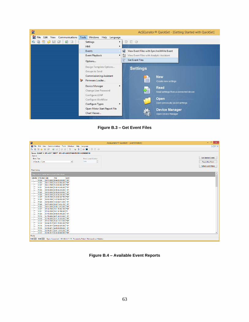
63
Figure B.3 – Get Event Files
Figure B.4 – Available Event Reports
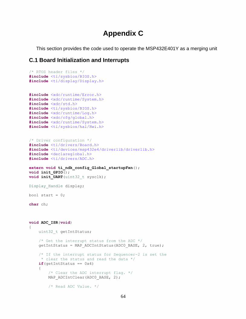
64
Appendix C
This section provides the code used to operate the MSP432E401Y as a merging unit
C.1 Board Initialization and Interrupts
/* RTOS header files */
#include <ti/sysbios/BIOS.h>
#include <ti/display/Display.h>
#include <xdc/runtime/Error.h>
#include <xdc/runtime/System.h>
#include <xdc/std.h>
#include <ti/sysbios/BIOS.h>
#include <xdc/runtime/Log.h>
#include <xdc/cfg/global.h>
#include <xdc/runtime/System.h>
#include <ti/sysbios/hal/Hwi.h>
/* Driver configuration */
#include <ti/drivers/Board.h>
#include <ti/devices/msp432e4/driverlib/driverlib.h>
#include <declareglobal.h>
#include <ti/drivers/ADC.h>
extern void ti_ndk_config_Global_startupFxn();
void init_GPIO();
void init_UART(uint32_t sysclk);
Display_Handle display;
bool start = 0;
char ch;
void ADC_ISR(void)
{
uint32_t getIntStatus;
/* Get the interrupt status from the ADC */
getIntStatus = MAP_ADCIntStatus(ADC0_BASE, 2, true);
/* If the interrupt status for Sequencer-2 is set the
* clear the status and read the data */
if(getIntStatus == 0x4)
{
/* Clear the ADC interrupt flag. */
MAP_ADCIntClear(ADC0_BASE, 2);
/* Read ADC Value. */
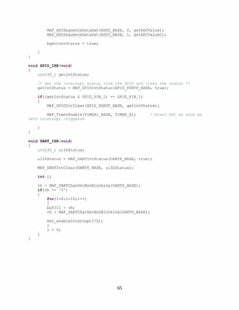
65
MAP_ADCSequenceDataGet(ADC0_BASE, 2, getADCValue);
MAP_ADCSequenceDataGet(ADC0_BASE, 1, getADCValueC);
bgetConvStatus = true;
}
}
void GPIO_ISR(void)
{
uint32_t getIntStatus;
/* Get the interrupt status from the GPIO and clear the status */
getIntStatus = MAP_GPIOIntStatus(GPIO_PORTF_BASE, true);
if((getIntStatus & GPIO_PIN_1) == GPIO_PIN_1)
{
MAP_GPIOIntClear(GPIO_PORTF_BASE, getIntStatus);
MAP_TimerEnable(TIMER1_BASE, TIMER_A); //start ADC as soon as
GPIO interrupt triggered
}
}
void UART_ISR(void)
{
uint32_t ui32Status;
ui32Status = MAP_UARTIntStatus(UART6_BASE, true);
MAP_UARTIntClear(UART6_BASE, ui32Status);
int i;
ch = MAP_UARTCharGetNonBlocking(UART6_BASE);
if(ch == '$')
{
for(i=0;i<15;i++)
{
buf[i] = ch;
ch = MAP_UARTCharGetNonBlocking(UART6_BASE);
Hwi_enableInterrupt(75);
}
i = 0;
}
}
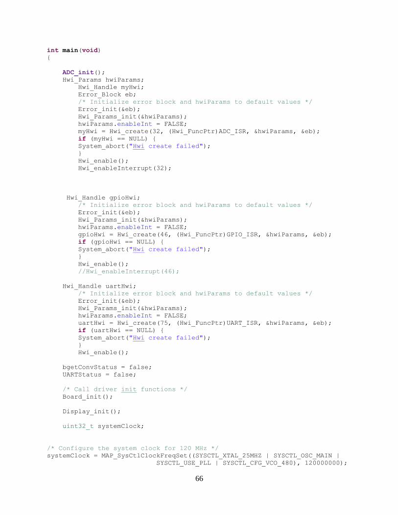
66
int main(void)
{
ADC_init();
Hwi_Params hwiParams;
Hwi_Handle myHwi;
Error_Block eb;
/* Initialize error block and hwiParams to default values */
Error_init(&eb);
Hwi_Params_init(&hwiParams);
hwiParams.enableInt = FALSE;
myHwi = Hwi_create(32, (Hwi_FuncPtr)ADC_ISR, &hwiParams, &eb);
if (myHwi == NULL) {
System_abort("Hwi create failed");
}
Hwi_enable();
Hwi_enableInterrupt(32);
Hwi_Handle gpioHwi;
/* Initialize error block and hwiParams to default values */
Error_init(&eb);
Hwi_Params_init(&hwiParams);
hwiParams.enableInt = FALSE;
gpioHwi = Hwi_create(46, (Hwi_FuncPtr)GPIO_ISR, &hwiParams, &eb);
if (gpioHwi == NULL) {
System_abort("Hwi create failed");
}
Hwi_enable();
//Hwi_enableInterrupt(46);
Hwi_Handle uartHwi;
/* Initialize error block and hwiParams to default values */
Error_init(&eb);
Hwi_Params_init(&hwiParams);
hwiParams.enableInt = FALSE;
uartHwi = Hwi_create(75, (Hwi_FuncPtr)UART_ISR, &hwiParams, &eb);
if (uartHwi == NULL) {
System_abort("Hwi create failed");
}
Hwi_enable();
bgetConvStatus = false;
UARTStatus = false;
/* Call driver init functions */
Board_init();
Display_init();
uint32_t systemClock;
/* Configure the system clock for 120 MHz */
systemClock = MAP_SysCtlClockFreqSet((SYSCTL_XTAL_25MHZ | SYSCTL_OSC_MAIN |
SYSCTL_USE_PLL | SYSCTL_CFG_VCO_480), 120000000);
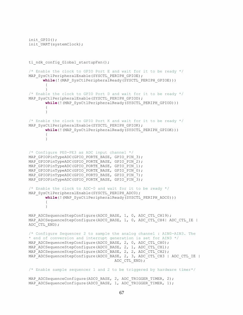
67
init_GPIO();
init_UART(systemClock);
ti_ndk_config_Global_startupFxn();
/* Enable the clock to GPIO Port E and wait for it to be ready */
MAP_SysCtlPeripheralEnable(SYSCTL_PERIPH_GPIOE);
while(!(MAP_SysCtlPeripheralReady(SYSCTL_PERIPH_GPIOE)))
{
}
/* Enable the clock to GPIO Port D and wait for it to be ready */
MAP_SysCtlPeripheralEnable(SYSCTL_PERIPH_GPIOD);
while(!(MAP_SysCtlPeripheralReady(SYSCTL_PERIPH_GPIOD)))
{
}
/* Enable the clock to GPIO Port K and wait for it to be ready */
MAP_SysCtlPeripheralEnable(SYSCTL_PERIPH_GPIOK);
while(!(MAP_SysCtlPeripheralReady(SYSCTL_PERIPH_GPIOK)))
{
}
/* Configure PE0-PE3 as ADC input channel */
MAP_GPIOPinTypeADC(GPIO_PORTE_BASE, GPIO_PIN_3);
MAP_GPIOPinTypeADC(GPIO_PORTE_BASE, GPIO_PIN_2);
MAP_GPIOPinTypeADC(GPIO_PORTE_BASE, GPIO_PIN_1);
MAP_GPIOPinTypeADC(GPIO_PORTE_BASE, GPIO_PIN_0);
MAP_GPIOPinTypeADC(GPIO_PORTD_BASE, GPIO_PIN_7);
MAP_GPIOPinTypeADC(GPIO_PORTK_BASE, GPIO_PIN_3);
/* Enable the clock to ADC-0 and wait for it to be ready */
MAP_SysCtlPeripheralEnable(SYSCTL_PERIPH_ADC0);
while(!(MAP_SysCtlPeripheralReady(SYSCTL_PERIPH_ADC0)))
{
}
MAP_ADCSequenceStepConfigure(ADC0_BASE, 1, 0, ADC_CTL_CH19);
MAP_ADCSequenceStepConfigure(ADC0_BASE, 1, 0, ADC_CTL_CH4| ADC_CTL_IE |
ADC_CTL_END);
/* Configure Sequencer 2 to sample the analog channel : AIN0-AIN3. The
* end of conversion and interrupt generation is set for AIN3 */
MAP_ADCSequenceStepConfigure(ADC0_BASE, 2, 0, ADC_CTL_CH0);
MAP_ADCSequenceStepConfigure(ADC0_BASE, 2, 1, ADC_CTL_CH1);
MAP_ADCSequenceStepConfigure(ADC0_BASE, 2, 2, ADC_CTL_CH2);
MAP_ADCSequenceStepConfigure(ADC0_BASE, 2, 3, ADC_CTL_CH3 | ADC_CTL_IE |
ADC_CTL_END);
/* Enable sample sequencer 1 and 2 to be triggered by hardware timer*/
MAP_ADCSequenceConfigure(ADC0_BASE, 2, ADC_TRIGGER_TIMER, 2);
MAP_ADCSequenceConfigure(ADC0_BASE, 1, ADC_TRIGGER_TIMER, 1);
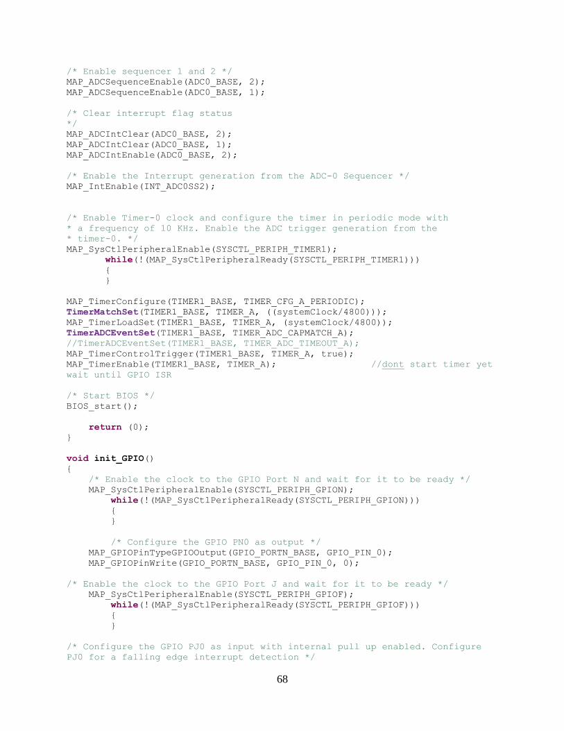
68
/* Enable sequencer 1 and 2 */
MAP_ADCSequenceEnable(ADC0_BASE, 2);
MAP_ADCSequenceEnable(ADC0_BASE, 1);
/* Clear interrupt flag status
*/
MAP_ADCIntClear(ADC0_BASE, 2);
MAP_ADCIntClear(ADC0_BASE, 1);
MAP_ADCIntEnable(ADC0_BASE, 2);
/* Enable the Interrupt generation from the ADC-0 Sequencer */
MAP_IntEnable(INT_ADC0SS2);
/* Enable Timer-0 clock and configure the timer in periodic mode with
* a frequency of 10 KHz. Enable the ADC trigger generation from the
* timer-0. */
MAP_SysCtlPeripheralEnable(SYSCTL_PERIPH_TIMER1);
while(!(MAP_SysCtlPeripheralReady(SYSCTL_PERIPH_TIMER1)))
{
}
MAP_TimerConfigure(TIMER1_BASE, TIMER_CFG_A_PERIODIC);
TimerMatchSet(TIMER1_BASE, TIMER_A, ((systemClock/4800)));
MAP_TimerLoadSet(TIMER1_BASE, TIMER_A, (systemClock/4800));
TimerADCEventSet(TIMER1_BASE, TIMER_ADC_CAPMATCH_A);
//TimerADCEventSet(TIMER1_BASE, TIMER_ADC_TIMEOUT_A);
MAP_TimerControlTrigger(TIMER1_BASE, TIMER_A, true);
MAP_TimerEnable(TIMER1_BASE, TIMER_A); //dont start timer yet
wait until GPIO ISR
/* Start BIOS */
BIOS_start();
return (0);
}
void init_GPIO()
{
/* Enable the clock to the GPIO Port N and wait for it to be ready */
MAP_SysCtlPeripheralEnable(SYSCTL_PERIPH_GPION);
while(!(MAP_SysCtlPeripheralReady(SYSCTL_PERIPH_GPION)))
{
}
/* Configure the GPIO PN0 as output */
MAP_GPIOPinTypeGPIOOutput(GPIO_PORTN_BASE, GPIO_PIN_0);
MAP_GPIOPinWrite(GPIO_PORTN_BASE, GPIO_PIN_0, 0);
/* Enable the clock to the GPIO Port J and wait for it to be ready */
MAP_SysCtlPeripheralEnable(SYSCTL_PERIPH_GPIOF);
while(!(MAP_SysCtlPeripheralReady(SYSCTL_PERIPH_GPIOF)))
{
}
/* Configure the GPIO PJ0 as input with internal pull up enabled. Configure
PJ0 for a falling edge interrupt detection */

69
MAP_GPIOPinTypeGPIOInput(GPIO_PORTF_BASE, GPIO_PIN_1);
GPIOF->PUR |= GPIO_PIN_1;
MAP_GPIOIntTypeSet(GPIO_PORTF_BASE, GPIO_PIN_1, GPIO_FALLING_EDGE);
MAP_GPIOIntEnable(GPIO_PORTF_BASE, GPIO_INT_PIN_1);
MAP_IntEnable(INT_GPIOF);
}
void init_UART(uint32_t sysclk)
{
MAP_SysCtlPeripheralEnable(SYSCTL_PERIPH_UART0);
MAP_SysCtlPeripheralEnable(SYSCTL_PERIPH_UART6);
MAP_SysCtlPeripheralEnable(SYSCTL_PERIPH_GPIOA);
MAP_SysCtlPeripheralEnable(SYSCTL_PERIPH_GPIOP);
GPIOPinConfigure(GPIO_PP0_U6RX);
GPIOPinConfigure(GPIO_PP1_U6TX);
MAP_GPIOPinTypeUART(GPIO_PORTP_BASE, GPIO_PIN_0 | GPIO_PIN_1);
MAP_UARTConfigSetExpClk(UART6_BASE, sysclk, 9600,
(UART_CONFIG_WLEN_8 | UART_CONFIG_STOP_ONE
|
UART_CONFIG_PAR_NONE));
UARTFIFOEnable(UART6_BASE);
UARTFIFOLevelSet(UART6_BASE, UART_FIFO_TX1_8, UART_FIFO_RX7_8);
int d;
int c;
//Only print RMC data
char gpscmd[53];
sprintf(gpscmd, "$PMTK314,0,1,0,0,0,0,0,0,0,0,0,0,0,0,0,0,0,0,0*29\r\n");
for(d = 0;d < 53;d++)
{
MAP_UARTCharPut(UART6_BASE, gpscmd[d]);
}
//change baud rate
char baudcmd[21];
sprintf(baudcmd,"$PMTK251,115200*1F\r\n"); //change baud rate
for(c = 0;c<21;c++)
{
MAP_UARTCharPut(UART6_BASE, baudcmd[c]);
}
//update gps uart baud rate setting
MAP_UARTConfigSetExpClk(UART6_BASE, sysclk, 115200,(UART_CONFIG_WLEN_8 |
UART_CONFIG_STOP_ONE |UART_CONFIG_PAR_NONE));
MAP_IntMasterEnable();
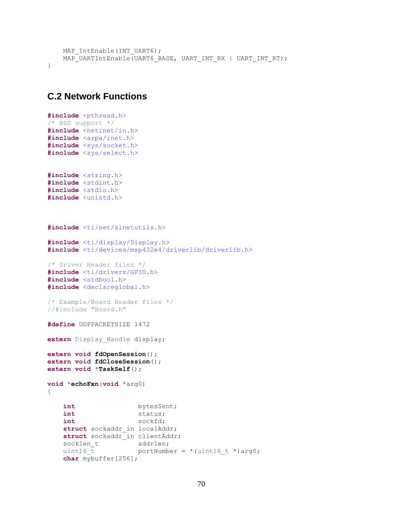
70
MAP_IntEnable(INT_UART6);
MAP_UARTIntEnable(UART6_BASE, UART_INT_RX | UART_INT_RT);
}
C.2 Network Functions
#include <pthread.h>
/* BSD support */
#include <netinet/in.h>
#include <arpa/inet.h>
#include <sys/socket.h>
#include <sys/select.h>
#include <string.h>
#include <stdint.h>
#include <stdio.h>
#include <unistd.h>
#include <ti/net/slnetutils.h>
#include <ti/display/Display.h>
#include <ti/devices/msp432e4/driverlib/driverlib.h>
/* Driver Header files */
#include <ti/drivers/GPIO.h>
#include <stdbool.h>
#include <declareglobal.h>
/* Example/Board Header files */
//#include "Board.h"
#define UDPPACKETSIZE 1472
extern Display_Handle display;
extern void fdOpenSession();
extern void fdCloseSession();
extern void *TaskSelf();
void *echoFxn(void *arg0)
{
int bytesSent;
int status;
int sockfd;
struct sockaddr_in localAddr;
struct sockaddr_in clientAddr;
socklen_t addrlen;
uint16_t portNumber = *(uint16_t *)arg0;
char mybuffer[256];
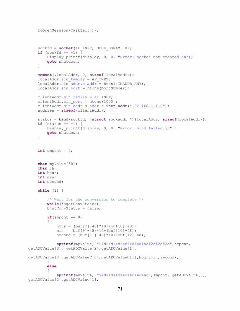
71
fdOpenSession(TaskSelf());
sockfd = socket(AF_INET, SOCK_DGRAM, 0);
if (sockfd == -1) {
Display_printf(display, 0, 0, "Error: socket not created.\n");
goto shutdown;
}
memset(&localAddr, 0, sizeof(localAddr));
localAddr.sin_family = AF_INET;
localAddr.sin_addr.s_addr = htonl(INADDR_ANY);
localAddr.sin_port = htons(portNumber);
clientAddr.sin_family = AF_INET;
clientAddr.sin_port = htons(1000);
clientAddr.sin_addr.s_addr = inet_addr("192.168.1.110");
addrlen = sizeof(clientAddr);
status = bind(sockfd, (struct sockaddr *)&localAddr, sizeof(localAddr));
if (status == -1) {
Display_printf(display, 0, 0, "Error: bind failed.\n");
goto shutdown;
}
int smpcnt = 0;
char myValue[50];
char ch;
int hour;
int min;
int second;
while (1) {
/* Wait for the conversion to complete */
while(!bgetConvStatus);
bgetConvStatus = false;
if(smpcnt == 0)
{
hour = (buf[7]-48)*10+(buf[8]-48);
min = (buf[9]-48)*10+(buf[10]-48);
second = (buf[11]-48)*10+(buf[12]-48);
sprintf(myValue, "%4d%4d%4d%4d%4d%4d%4d%2d%2d%2d",smpcnt,
getADCValue[3], getADCValue[2],getADCValue[1],
getADCValue[0],getADCValueC[0],getADCValueC[1],hour,min,second);
}
else
{
sprintf(myValue, "%4d%4d%4d%4d%4d%4d%4d",smpcnt, getADCValue[3],
getADCValue[2],getADCValue[1],
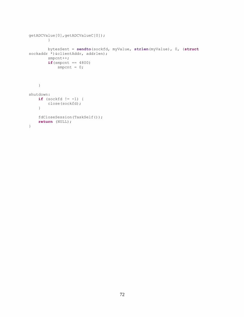
72
getADCValue[0],getADCValueC[0]);
}
bytesSent = sendto(sockfd, myValue, strlen(myValue), 0, (struct
sockaddr *)&clientAddr, addrlen);
smpcnt++;
if(smpcnt == 4800)
smpcnt = 0;
}
shutdown:
if (sockfd != -1) {
close(sockfd);
}
fdCloseSession(TaskSelf());
return (NULL);
}