Embed Size (px)
Citation preview
eScholarship provides open access, scholarly publishingservices to the University of California and delivers a dynamicresearch platform to scholars worldwide.
Electronic Theses and DissertationsUC Santa Cruz
Peer Reviewed
Title:Characterization Of High-Stroke High-Aspect Ratio Micro Electro Mechanical SystemsDeformable Mirrors For Adaptive Optics
Author:Bouchti, Mohamed Amine
Acceptance Date:2013
Series:UC Santa Cruz Electronic Theses and Dissertations
Degree:M.S., Electrical EngineeringUC Santa Cruz
Advisor(s):Kubby, Joel
Committee:Kubby, Joel, Kobayashi, Nobuhiko, Gavel, Don
Permalink:http://escholarship.org/uc/item/26h990mc
Abstract:
Copyright Information:All rights reserved unless otherwise indicated. Contact the author or original publisher for anynecessary permissions. eScholarship is not the copyright owner for deposited works. Learn moreat http://www.escholarship.org/help_copyright.html#reuse

UNIVERSITY OF CALIFORNIA
SANTA CRUZ
Characterization Of High-‐Stroke High-‐Aspect Ratio Micro Electro Mechanical Systems Deformable Mirrors
For Adaptive Optics
A thesis submitted in partial satisfaction of the requirements for the degree of
MASTER OF SCIENCE
in
ELECTRICAL ENGINEERING
by
Mohamed Amine Bouchti
June 2013
The Thesis of Mohamed Amine Bouchti is approved:
___________________________________
Professor Joel A. Kubby, Chair
___________________________________ Professor Nobuhiko Kobayashi
___________________________________
Don Gavel, Director of the Laboratory for Adaptive Optics, UCSC
_____________________________ Tyrus Miller Vice Provost and Dean of Graduate Studies

Copyright © by Mohamed Amine Bouchti
2013

iii
Table of Contents
List of Figures v List of Tables ix Abstract x Dedications xii Acknowledgement xiii Chapter 1: Introduction 1
1.1 Introduction 1 1.2 MEMS Actuators 3 1.3 Deformable Mirror Fabrication 8 1.4 X-Beam Design 12
Chapter 2: Deformable Mirror Testing 16 2.1: Actuator Packaging and PCB Test Board 16 2.2: WYKO Interferometer 20 2.3: Testing Procedure 22 Chapter 3: Deformable Mirror Testing Results 29 3.1: Challenges 29 3.2: Results 36 3.2.1: Individual Actuator Testing 37 3.2.2: Two-Actuators Testing 39
iv
3.3: Summary/Discussion 46 Chapter 4: Future Work 54 4.1: Individual Actuator Testing 54 4.2 Dual Actuator Testing 57 4.3: Future work 61 Chapter 5: Conclusion 63 Bibliography 64

v
List of Figures Figure 1.1: Schematic of parallel light Rays (Left) vs. rays affected by turbulence 1 Figure 1.2: Schematic of adaptive optics system 2 Figure 1.3: Shack Hartman wavefront sensor 2 Figure 1.4: Parallel plate actuator mode 3 Figure 1.5: Monolithic fabrication process overview. (A) Patterning, electroplating, and CMP of counter electrodes and anchor post. (B) Patterning, electroplating, and CMP of the spring layer. (C) Patterning, electroplating, and CMP of the mirror support post and of the mirror layer. (D) Released continuous facesheet mirror attached to actuators 9 Figure 1.6: 3D actuator designs modeled with FEA. (A) Square actuators supported by eight folded springs at the corners. (B) Circular actuators supported by four folded springs. (C) X-beam actuators supported by four fixed-guided beams 11 Figure 1.7: The three actuator’s designs shown in Figure 1.6 fabricated out of gold 12 Figure 1.8: Fixed-fixed beam subjected to a point load F at the middle of the beam 13 Figure 1.9: layout of 16x16 deformable mirror array 15
Figure 1.10: Close-up view of the top right of a 16x16 deformable mirror array 15
Figure 2.1: Packaged Deformable Mirror 16
Figure 2.2: PCB layout for 16x16 deformable mirror 17
Figure 2.3: Location of the center 4x4 Actuator of the deformable mirror in the ZIF Socket 18 Figure 2.4: ZIF Socket Mounted on the fabricated PCB 19
Figure 2.5: represents the flow chart of the VSI algorithm used to extract the interference signal 20
Figure 2.6: Schematic representation of the Veeco WYKO interferometer 21

vi
Figure 2.7: Image of the WYKO interferometer used for testing the deformable mirrors 21 Figure 2.8: Fringes of the deformable mirror 23
Figure 2.9: Surface Scan of a deformable mirror before alignment 24
Figure 2.10: Surface Scan of a deformable mirror after alignment 24
Figure 2.11: Window for setting the maximum slope and minimum islands 25
Figure 2.12: Window for defining the actuators of interests and references 26
Figure 2.13: Window after finishing the set up and calculating the initial heights of the actuators of interest 27 Figure 2.14: Database view and graphs of displacement vs. voltage for dual actuator testing. 28 Figure 3.1: Displacement vs. voltage for a 10x10 mirror system 29 Figure 3.2: Oscillating behavior in the Displacement vs. voltage graph for a dual actuator-system testing 31 Figure 3.3: Probe station used for electrical and mechanical probing 32
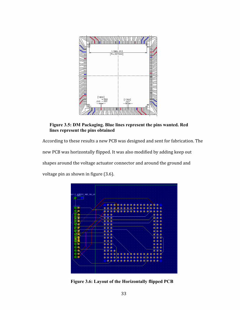
Figure 3.4: ZIF socket pin array. Blue dots represent the pins wanted. Red dots represent the pins obtained 32 Figure 3.5: DM Packaging. Blue lines represent the pins wanted. Red lines represent the pins obtained 33 Figure 3.6: Layout of the Horizontally flipped PCB 33
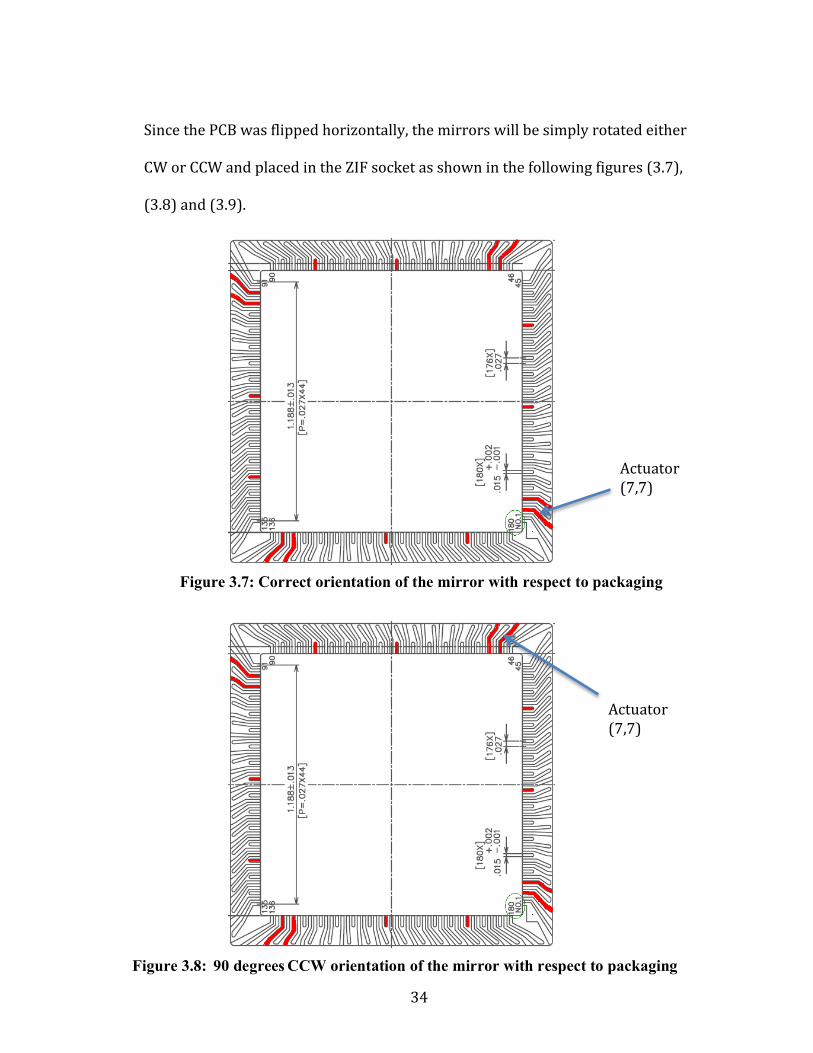
Figure 3.7: Correct orientation of the mirror with respect to packaging 34 Figure 3.8: 90 degrees CCW rotation of the mirror with respect to packaging 34 Figure 3.9: 90 degrees CW rotation of the mirror with respect to packaging 35 Figure 3.10: Center 4 x 4 actuators of the deformable mirror with the hole in the top 36
vii
Figure 3.11: Graph of voltage vs. displacement for actuator (7,7) 37
Figure 3.12: Graph of voltage vs. displacement for actuator (10,7) 38
Figure 3.13: Graph of voltage vs. displacement for actuator (10,8) 38
Figure 3.14: Trial 1 for dual actuator testing for actuator (7,7) and (7,8) 39
Figure 3.15: Trial 2 for dual actuator testing for actuator (7,7) and (7,8) 40
Figure 3.16: Trial 3 for dual actuator testing for actuator (7,7) and (7,8) 40
Figure 3.17: Trial 1 for dual actuator testing for actuator (10,7) and (10,8) 41
Figure 3.18: Trial 2 for dual actuator testing for actuator (10,7) and (10,8) 42
Figure 3.19: Trial 3 for dual actuator testing for actuator (10,7) and (10,8) 42
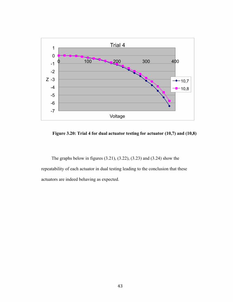
Figure 3.20: Trial 4 for dual actuator testing for actuator (10,7) and (10,8) 43
Figure 3.21: Repeatability of actuator (7,7) throughout the 3 trials 44
Figure 3.22: Repeatability of actuator (7,8) throughout the 3 trials 44
Figure 3.23: Repeatability of Actuator (10,7) throughout the four trials 45
Figure 3.24: Repeatability of Actuator (10,7) throughout the four trials 45
Figure 3.25: Height of actuators located in the corner of the deformable mirror as well as the height of actuators in the middle of each side of the mirror 48 Figure 3.26: Average height from the substrate to the mirror layer, from the substrate to the spring layer and for the counter electrode of this deformable mirror 49 Figure 3.27: An illustration of a test-structure (bulls-eye) found around the mirror 50 Figure 3.28: Standard Paschen curve, modified Paschen curve, Vacuum breakdown, and safe operating region for MEMS for air at one atmosphere 53
Figure 4.1: Image of the Center 4 x 4 X-Beam Actuators 54
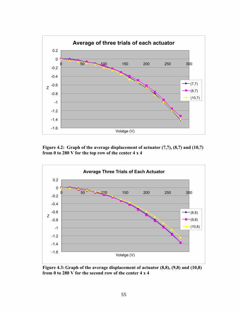
Figure 4.2: Graph of the average displacement of actuator (7,7), (8,7) and (10,7) from 0 to 280 V for the top row of the center 4 x 4 55

viii
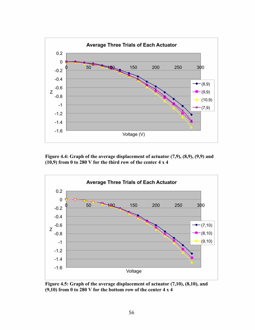
Figure 4.3: Graph of the average displacement of actuator (8,8), (9,8) and (10,8) from 0 to 280 V for the second row of the center 4 x 4 55 Figure 4.4: Graph of the average displacement of actuator (7,9), (8,9), (9,9) and (10,9) from 0 to 280 V for the third row of the center 4 x 4 56 Figure 4.5: Graph of the average displacement of actuator (7,10), (8,10), and (9,10) from 0 to 280 V for the bottom row of the center 4 x 4 56 Figure 4.6: Repeatability of Actuator (7,7) throughout the four Trials of dual actuator testing of the second DM 57 Figure 4.7: Repeatability of Actuator (7,8) throughout the four Trials of dual actuator testing of the second DM 58 Figure 4.8: Repeatability of Actuator (7,9) throughout the four Trials of dual actuator testing of the second DM 58 Figure 4.9: Repeatability of Actuator (7,10) throughout the four Trials of dual actuator testing of the second DM 59 Figure 4.10: Repeatability of Actuator (8,7) throughout the four Trials of dual actuator testing of the second DM 59 Figure 4.11: Repeatability of Actuator (8,8) throughout the four Trials of dual actuator testing of the second DM 60 Figure 4.12: Repeatability of Actuator (8,9) throughout the four Trials of dual actuator testing of the second DM 60 Figure 4.13: Repeatability of Actuator (8,9) throughout the four Trials of dual actuator testing of the second DM 61
ix
List of Tables
Table 2.1: The Die pad name, Die pad number and the equivalent package pad number of the center 4x4 actuators 18
Table 3.1: The maximum displacement of actuators (7,7) and (7,8) in pair actuator testing in all trials 46 Table 3.2: The maximum displacement of actuators (10,7) and (10,8) in pair actuator testing in all trials 46 Table 3.3: Comparison of the displacement between single and dual actuation for each actuator 47 Table 3.4: Summary of the heights of the counter electrode, the gap between the counter electrode and spring layer, the post gap, the mirror layer and the total height of each bulls-eye that are part of the DM. 50 Table 3.5: Summary of the heights of the counter electrode, the gap between the counter electrode and spring layer, the post gap, the mirror layer and the total height of bulls-eyes that are not part of the 51 Table 3.6: Comparison between the heights of the counter electrode, the gap between the counter electrode and spring layer, the post gap, the mirror layer and the total height of bulls-eyes that are part of the DM and ones that are not part of the DM. 52

x
Abstract
Characterization Of High-Stroke High-Aspect Ratio Micro Electro Mechanical Systems Deformable Mirrors For Adaptive
Optics
Mohamed Amine Bouchti
Adaptive optics MEMS deformable mirror, in conjunction with Shack Hartman
wave front sensor and real-time controller, is capable of correcting time-varying
aberrations in imaging applications through manipulating its mirror surface. Adaptive
optics systems in astronomy for next generation large telescopes (30 meter primary
mirrors) require a high stroke of 10µm of mechanical displacement. This required
stroke would be achieved by MEMS deformable mirrors fabricated with high aspect
ratio techniques.
This thesis will review the designs of various types of high aspect actuators
consisting of folded springs with rectangular and circular membranes as well as X-
beam actuators. Finite element analysis (FEA) simulations of these designs have
shown the ability of each design to achieve a stroke of approximately 9.4 µm. Also,
FEA simulations proved that the X-beam actuators provide the best spring support
while preventing tilting.
In addition, this thesis will discuss device characterization and voltage vs.
displacement test results for the high aspect ratio gold MEMS 16 x 16 X-‐beam

xi
actuators deformable mirror that has been bonded and packaged. The results
have shown that the device is capable of achieving approximately 5.5 µm in
individual actuator testing and 7µm in dual actuator testing.

xii
To my parents Bouchti Ahmed and Moutawakkil Halima, to my sisters and my brother Laila, Tarik and Hanane Bouchti
to my wife Josie and her dad Richard Moss to my brother-‐in-‐law Richard King and my Friend Erin
McGinty.

xiii
Acknowledgements
I would like to thank my research advisor Dr. Joel A. Kubby for his support
and guidance and the other members of my committee, Dr. Donald T. Gavel and
Dr. Nobuhiko Kobayashi. I would also thank the Initiative for Maximizing
Student Diversity (IMSD) funded through NIGMS, NIH for giving me the
opportunity and the support during my first two years of graduate school.
I would like to thank Baustista Fernandez for his support and guidance. I
would also like to thank my family, my wife and friends for their love, support
and encouragement that allowed me to be at this stage of my life.
I would also like to thank the MEMS Research Laboratory group at UC Santa
Cruz, especially, Dmitry Medved, Oscar Azucena, Zachary Graham, Andrew Norton,
Dan O'Leary, Marco Reinig, and Xiaodong Tao for taking the time to attend my
presentations and provide me with valuable feedbacks.
1
Chapter 1: Introduction
1.1 Introduction
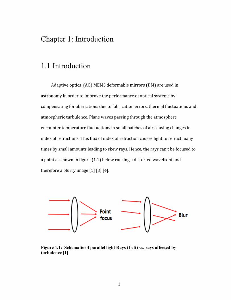
Adaptive optics (AO) MEMS deformable mirrors (DM) are used in
astronomy in order to improve the performance of optical systems by
compensating for aberrations due to fabrication errors, thermal fluctuations and
atmospheric turbulence. Plane waves passing through the atmosphere
encounter temperature fluctuations in small patches of air causing changes in
index of refractions. This flux of index of refraction causes light to refract many
times by small amounts leading to skew rays. Hence, the rays can’t be focused to
a point as shown in figure (1.1) below causing a distorted wavefront and
therefore a blurry image [1] [3] [4].
Figure 1.1: Schematic of parallel light Rays (Left) vs. rays affected by turbulence [1]

2
The main components of an AO system, as shown in figure (1.2), are a
wavefront sensor, a control system and a deformable mirror. Shack-‐Hartman
wavefront sensor (SHWFS) is used to measure the distorted wavefront. This
sensor splits light into a number of small beams using an array of miniature
lenses, called lenslets. The light from each of these lenslets is focused onto a CCD
camera as shown in figure (1.3) below. As the portion of the wavefront hitting
the lenslet is aberrated, the focused spot on the CCD camera moves. Through
simple geometry using the displacement of the focused spot and the focal length
of the lenslet, the local tilt of the wavefront is approximated [1] [2] [9].
Figure 1.2: Schematic of adaptive optics system [1]
Figure 1.3: Shack Hartman wavefront sensor [2]

3
Once the wavefront is measured, a control system (typically a computer
running control algorithm software) calculates the appropriate shape needed to
compensate the wavefront and sends that information to the deformable mirror.
The deformable mirror changes the spatial phase of a wavefront using an array
of actuators that deforms the mirror’s surface. The appropriate shape of the
mirror to compensate for each aberration is simply the same shape as the
wavefront with half the amplitude since the reflection doubles the effect [1] [2].
1.2 MEMS Actuators
The actuators of the deformable mirrors are electrostatically actuated and
move in a piston like motion. Each actuator is modeled as a two parallel-‐plate
capacitor with gap g between them, area A and dielectric constant ε. The top
plate is connected to a spring and it is free to move, while the bottom plate is
fixed to the substrate as shown in figure (1.4). Applying a voltage V results in an
attractive electrostatic force Fe that bends the actuator membrane downward.
Figure 1.4: Parallel plate actuator mode [3]

4
This electrostatic force is related to the mechanical work done from the outside
in moving the plate by a distance Z, which is given by equation (1.1):
While the electric work, if we control the voltage and let charge flow into the
capacitor from a battery, is given by equation (1.2):
In addition, the work required in charging the capacitor due to a change in
charge Q at constant voltage is given by equation (1.3) as follow:
!W = Fe " !Z (1.1)
!We = !q "V = V " !C( ) "V =V 2 " !C (1.2)
dU =V !dq
dU =QC!dq where Q = C !V
U =QC!dq = 1
2!Q2
C"
U =12C !V 2 (1.3)

5
The electrostatic force is found by balancing the change in the potential energy
in the capacitors with the sum of the mechanical work and the electric work as
follows:
The capacitance of the parallel plates is given by the (1.5):
And therefore the electrostatic force becomes:
!UCapacitor = !WMechanical +!WElectrical
12V 2 " !C = Fe " !Z +V
2 " !C
#12V 2 " !C = Fe " !Z
Fe = #12V 2 "
!C!Z
(1.4)
C = ! !Ag0 " z
where g = g0 - z (1.5)
Fe = !12V 2 "
dCdz
Fe = !12V 2 "
ddz
! "Ag0 ! z#
$%
&
'(
Fe = !12V 2 "
!! "Ag0 ! z( )2
#
$%%
&
'((
6
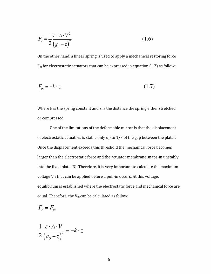
On the other hand, a linear spring is used to apply a mechanical restoring force
Fm for electrostatic actuators that can be expressed in equation (1.7) as follow:
Where k is the spring constant and z is the distance the spring either stretched
or compressed.
One of the limitations of the deformable mirror is that the displacement
of electrostatic actuators is stable only up to 1/3 of the gap between the plates.
Once the displacement exceeds this threshold the mechanical force becomes
larger than the electrostatic force and the actuator membrane snaps-‐in unstably
into the fixed plate [3]. Therefore, it is very important to calculate the maximum
voltage Vpi that can be applied before a pull-‐in occurs. At this voltage,
equilibrium is established where the electrostatic force and mechanical force are
equal. Therefore, the Vpi can be calculated as follow:
Fe =12! !A !V 2
g0 " z( )2 (1.6)
Fm = !k " z (1.7)
Fe = Fm
12! !A !Vg0 " z( )2
= "k ! z

7
Solving for V as a function of Z we get:
And evaluating z at 1/3 of the gap leads to the pull-‐in voltage given by equation
(1.7)[3]:
V =2 ! k ! z ! g0 " z( )
! !A
V =2 ! k ! z ! g0 " z( )
! !Az=g0
3
Vpi =8 ! k ! g0
3
27 !! !A (1.8)

8
1.3 Deformable Mirror Fabrication
Adaptive optics applications in astronomy require a high stroke of 10μm of
mechanical displacement. However, current deformable mirrors are fabricated
using surface micromachining techniques that provide only a stroke of less than
6μm for continuous-‐facesheet mirrors. Commercial MEMS deformable mirrors
developed by Boston Micromachines Corporation provide a stroke between 1.5
to 5.5μm. This limitation is due to the fact that the sacrificial oxide layer in the
surface micromachining process is limited to a thin-‐film of 2μm [4].
Dr. Kubby and Dr. Fernandez have fabricated deformable mirrors with
MEMS high-‐stroke actuators using high aspect ratio Innovative Micro
Technologies (IMT). IMT uses a monolithic fabrication process that allows for
thick layer deposition, between 10 to 100μm, of sacrificial layer and therefore
allowing for a 10μm stroke required for astronomical applications [5].
This process is performed on optically flat WMS-‐15 glass-‐ceramic
substrates with thermal expansion of 11.4 x 10-‐6 K-‐1 (close to the coefficient of
thermal expansion of gold, which is 14.2 x 10-‐6 K-‐1) and involves four phases. The
first phase, as shown in figure (1.5a), in the fabrication starts with a deposition, a
lift off and then a patterning of a 0.5μm electrode layer on the substrate. The
next step is the patterning and electroplating of the gold actuator anchors to a
height of 22μm. The electroplated gold anchors and copper sacrificial layer are
planarized down to a height of approximately 20μm with a chemical mechanical

9
planarization (CMP) process. The next phase involves the patterning and
electroplating of a 4μm gold spring layer followed by a copper electroplating up
to the height of the spring layer. In addition, these layers undergo CMP
planarization as shown in figure (1.5b). The third phase incorporates 30μm of
patterned and electroplated mirror support posts and an electroplated copper
sacrificial layer. Once again, the electroplated mirror post and the sacrificial
layer are planarized using CMP as shown in figure (1.5c). In addition, a 2μm gold
mirror layer is patterned electroplated and then planarized to an optical mirror.
And finally, a chemical etching step is required to remove the copper sacrificial
layer resulting in an approximately 56.5μm high released structure as illustrated
in figure (1.5d) [4] [5].
Figure 1.5: Monolithic fabrication process overview. (A) Patterning, electroplating, and CMP of counter electrodes and anchor post. (B) Patterning, electroplating, and CMP of the spring layer. (C) Patterning, electroplating, and CMP of the mirror support post and of the mirror layer. (D) Released continuous facesheet mirror attached to actuators [6].
10
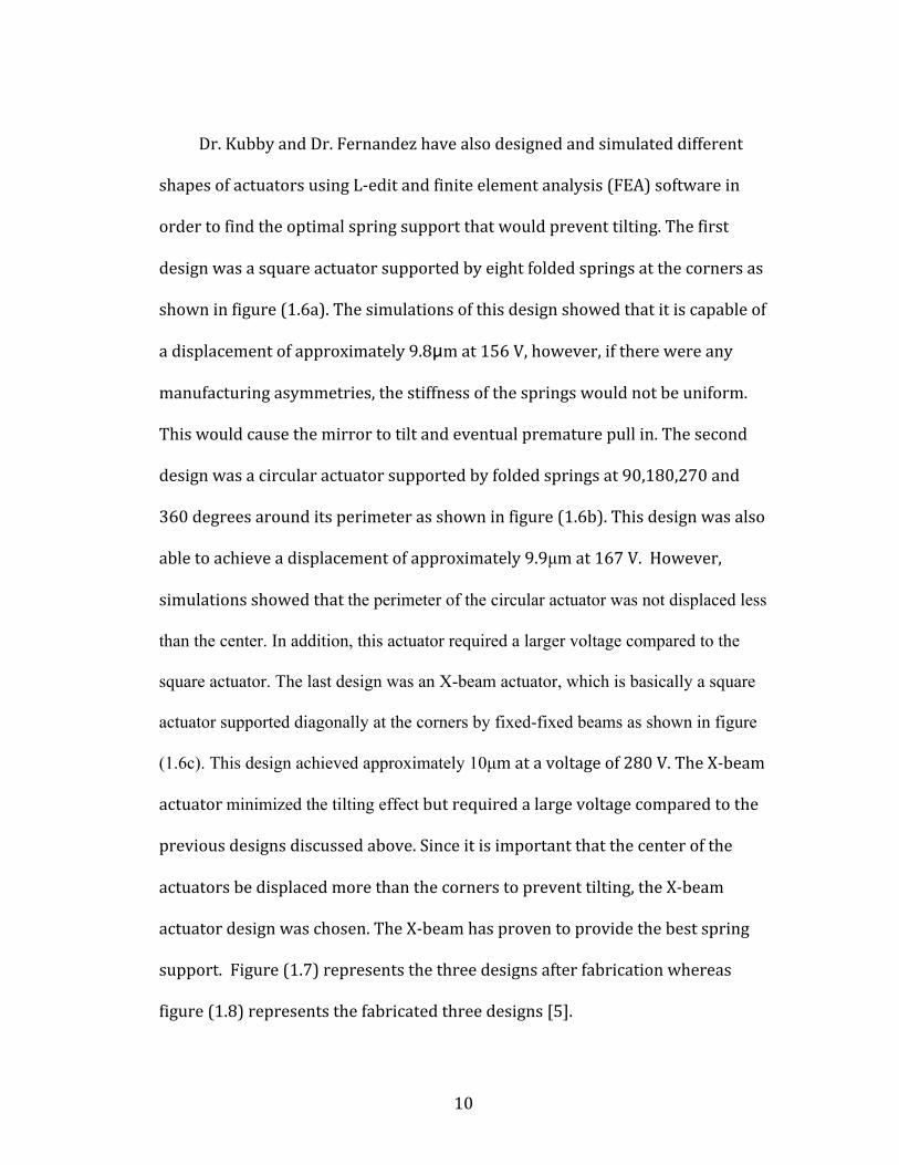
Dr. Kubby and Dr. Fernandez have also designed and simulated different
shapes of actuators using L-‐edit and finite element analysis (FEA) software in
order to find the optimal spring support that would prevent tilting. The first
design was a square actuator supported by eight folded springs at the corners as
shown in figure (1.6a). The simulations of this design showed that it is capable of
a displacement of approximately 9.8μm at 156 V, however, if there were any
manufacturing asymmetries, the stiffness of the springs would not be uniform.
This would cause the mirror to tilt and eventual premature pull in. The second
design was a circular actuator supported by folded springs at 90,180,270 and
360 degrees around its perimeter as shown in figure (1.6b). This design was also
able to achieve a displacement of approximately 9.9µm at 167 V. However,
simulations showed that the perimeter of the circular actuator was not displaced less
than the center. In addition, this actuator required a larger voltage compared to the
square actuator. The last design was an X-beam actuator, which is basically a square
actuator supported diagonally at the corners by fixed-fixed beams as shown in figure
(1.6c). This design achieved approximately 10µm at a voltage of 280 V. The X-‐beam
actuator minimized the tilting effect but required a large voltage compared to the
previous designs discussed above. Since it is important that the center of the
actuators be displaced more than the corners to prevent tilting, the X-‐beam
actuator design was chosen. The X-‐beam has proven to provide the best spring
support. Figure (1.7) represents the three designs after fabrication whereas
figure (1.8) represents the fabricated three designs [5].

11
Figure 1.7: The three actuator’s designs shown in Figure 1.6 fabricated out of gold [5].
Figure 1.6: 3D actuator designs modeled with FEA. (A) Square actuators supported by eight folded springs at the corners. (B) Circular actuators supported by four folded springs. (C) X-beam actuators supported by four fixed-guided beams [5].

12
1.4 X-Beam Actuator Design
The X-beam actuators were designed to prevent premature pull-in while
achieving large displacement. The center square electrode in the x-beam actuator
measures 400 x 400µm with four 390 x 20µm fixed-guided beams as shown in figure
(1.6c). The actuator’s fixed-guided beams become nonlinear when displaced by more
than half of the spring layer thickness. This nonlinearity allows for mechanical strain
or stiffening to increase the actuators travel range to more than half the gap [7].
Therefore, the actuator’s spring can be described by a nonlinear spring equation as
follows:
And the pull-‐in voltage becomes:
Where K is the linear spring constant and KS is the nonlinear stretching component.
The linear MEMS spring constant is calculated by assuming that the actuator’s beams
are two parallel fixed-fixed beams as shown in figure (1.8):
Fm = K ! z+Ks ! z3 (1.9)
Vpi =2 ! K ! z+Ks ! z
3( ) ! g0 " z( )2
! !A (1.10)

13
Figure 1.8: Fixed-fixed beam subjected to a point load F at the middle of the beam [3].
This spring constant is a function of Young’s Modulus (E), the length of the spring’s
beam (L) and the moment of inertia (I) as given by the following equation:
Since the moment of inertia is given by
Where w and t are the width and thickness of the spring beams, respectively.
Therefore the spring constant K becomes:
K =384 !E ! I
L3 (1.11)
I = w ! t3
12 (1.12)
K =384 !EL3 ! w ! t
3
12
K =32 !E !w ! t3
L3 (1.13)

14
Similarly, the nonlinear stretching component for a single fixed-‐fixed beam is
given by the following equation:
And for two fixed-‐fixed beams the equation becomes:
Therefore the mechanical force becomes:
The deformable mirrors discussed in this thesis consist of 16 x 16 array of
actuators with a continuous facesheet as shown in figure (1.9). The inner
14 x 14 actuators can be tested individually from each other as well as in groups
for multi-‐actuator testing. Each electrode in each actuator is routed and
connected to a bond pad [6].
Ks =! 4 !E !w ! t8 !L2
Ks =! 4 !E !w ! t
4 !L2 (1.14)
Fm =32 !E !w ! t3
L3 ! z+ !4 !E !w ! t4 !L2 ! z3 (1.15)

15
Figure 1.9: layout of 16x16 deformable mirror array [6]
Figure 1.10: Close-up view of the top right of a 16x16 deformable mirror array [6]

16
Chapter 2: Deformable Mirror Testing 2.1 Actuator Packaging and PCB Test Board
The 16 x 16 actuator deformable mirrors were packaged onto a 181 gold-
plated through-hole ceramic pin grid array (CPGA) as shown in figure (2.1). In order
to actuate the largest number of actuators in a square area, the center 12 x 12
actuators were wire-bonded to the CPGA where the outer 2 rows of the deformable
mirror are used as spring support for the continuous facesheet. In addition, these
deformable mirrors were not hermetically sealed. A glass lid was taped to protect the
mirrors from dust [6].
Figure 2.1: Packaged Deformable Mirror

17
The center 4 × 4 actuators of DMs were utilized for multi-actuator
displacement testing. In order to perform the DM testing, a PCB was designed and
fabricated as shown in figure (2.2). The PCB consists of two layers: the top layer,
where the yellow traces are located and the bottom layer where the red traces are
located. Also, the PCB has a ground plane (blue layer) at the bottom layer to help
reduce noise. The PCB allows the actuation of 1 to 16 actuators with a single power
supply by shorting a pin attached to a trace leading to the actuator of interest and a
power pin. The deformable mirrors continuous facesheet is attached to the power
supplies’ ground. The packaged deformable mirrors were placed on a zero insertion
force (ZIF) PGA test and burn-in socket (181-PRS 18041-12, Aries Electronics, Inc,
Bristol, Pennsylvania) allowing the DMs to be easily swapped for testing. Table (2.1)
gives the Die pad name (location of the actuator in the mirror layout), Die pad
number and the equivalent package pad number of the center 4 x 4 actuators.
Figure (2.3) shows the location of the actuators on the ZIF sockets, and figure
(2.4) is an image of the ZIF socket mounted on the fabricated PCB.
Figure 2.2: PCB layout for 16x16 deformable mirror

18
Table 2.1: The Die pad name, Die pad number and the equivalent package pad number of the center 4x4 actuators
Figure 2.3: Location of the center 4x4 Actuator of the deformable mirror in the ZIF Socket

19
Figure 2.4: ZIF Socket Mounted on the fabricated PCB

20
2.2 WYKO Interferometer:
The Veeco WYKO ® NT1100 interferometer is used to test the deformable
mirrors. This interferometer is an optical profiler providing accurate three-
dimensional measurement of the surface topography of systems, ranging from a
crystal surface to a MEMS deformable mirror. In this interferometer, the light reflects
off of a reference mirror and combines with light from a sample to produce
interference fringes. These fringes are alternating bright and dark bands of light. At
the point of best contrast, we are able to obtain the best focus. The interferometer is
able to take measurements via optical Phase-Shifting (PSI) and white light Vertical
Scanning (VSI) and then outputs the scans and data to the WYKO Vision Software
for analysis. In the testing of the deformable mirrors, the VSI mode is used. In this
mode the white-light source is filtered with a neutral density filter, which preserves
the short coherence length of the white light, and the system measures the degree of
fringe modulation, or coherence, instead of the phase of the interference fringes [8].
Figure (2.5) represents the flow chart of the VSI algorithm used to extract the
interference signal. Figure (2.6) gives a schematic of the interferometer. And figure
(2.7) is an image of the WYKO interferometer.
Figure 2.5: represents the flow chart of the VSI algorithm used to extract the interference signal [8]

21
Figure 2.6: Schematic representation of the Veeco WYKO interferometer
Figure 2.7: Image of the WYKO interferometer used for testing the deformable mirrors

22
2.3 Testing Procedure
The following procedure describes how to set up the Veeco vision software and
apply voltage to actuate the deformable mirror using the WYKO interferometer:
1) Connect the power supply probes so that the ground probe is connected
to the ground bond pad and the voltage probe connected to the desired
actuator’s bond pad.
2) Click on measurement options to set measurement type to VSI, Objective
to 2X and the field of view (FOV) to 0.5X.
3) Under the same window click on VSI options to set the Backscan that is
the distance the camera will vertically move upwards to take
measurements. Set the length that is the downward distance measured.
And the threshold modulation, which is the percentage ratio where the
higher the percentage the higher the accuracy. The appropriate values for
testing the deformable mirrors discussed in this thesis are as follows:
Backscan: 10 μm Length: 80 μm Modulation Threshold: 1%
4) Fluff the fringes at the bottom layer and then bring them back to the top
layer. Align the fringes with the desired actuator as shown in figure (2.8)
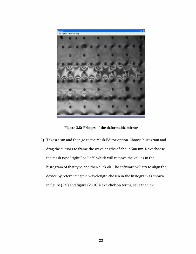
23
Figure 2.8: Fringes of the deformable mirror
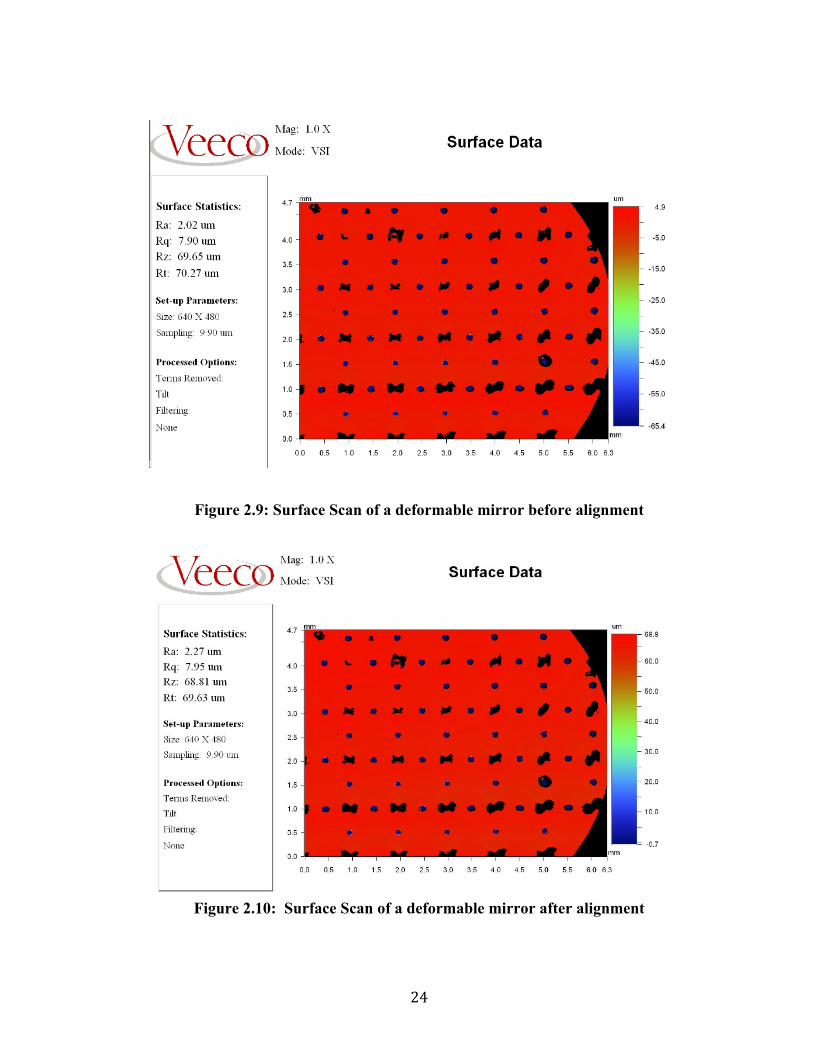
5) Take a scan and then go to the Mask Editor option. Choose histogram and
drag the cursors to frame the wavelengths of about 500 nm. Next choose
the mask type “right ” or “left” which will remove the values in the
histogram of that type and then click ok. The software will try to align the
device by referencing the wavelength chosen in the histogram as shown
in figure (2.9) and figure (2.10). Next, click on terms, save then ok.
24
Figure 2.9: Surface Scan of a deformable mirror before alignment
Figure 2.10: Surface Scan of a deformable mirror after alignment
25
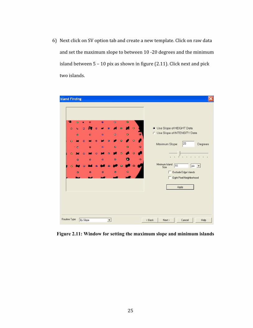
6) Next click on SV option tab and create a new template. Click on raw data
and set the maximum slope to between 10 -‐20 degrees and the minimum
island between 5 – 10 pix as shown in figure (2.11). Click next and pick
two islands.
Figure 2.11: Window for setting the maximum slope and minimum islands
26
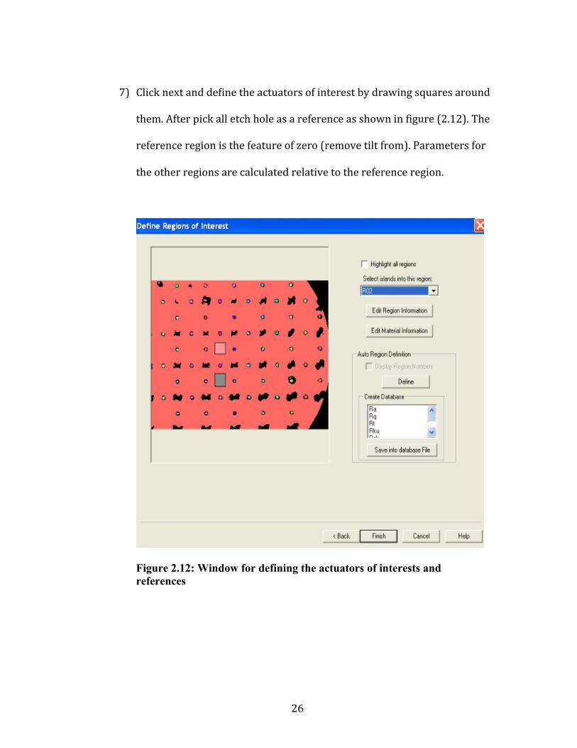
7) Click next and define the actuators of interest by drawing squares around
them. After pick all etch hole as a reference as shown in figure (2.12). The
reference region is the feature of zero (remove tilt from). Parameters for
the other regions are calculated relative to the reference region.
Figure 2.12: Window for defining the actuators of interests and references
27
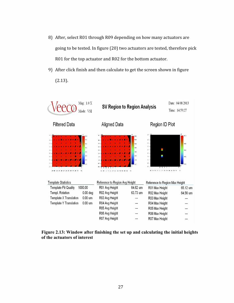
8) After, select R01 through R09 depending on how many actuators are
going to be tested. In figure (20) two actuators are tested, therefore pick
R01 for the top actuator and R02 for the bottom actuator.
9) After click finish and then calculate to get the screen shown in figure
(2.13).
Figure 2.13: Window after finishing the set up and calculating the initial heights of the actuators of interest
28
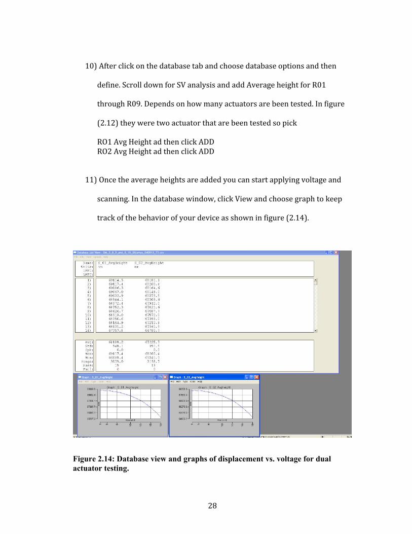
10) After click on the database tab and choose database options and then
define. Scroll down for SV analysis and add Average height for R01
through R09. Depends on how many actuators are been tested. In figure
(2.12) they were two actuator that are been tested so pick
RO1 Avg Height ad then click ADD RO2 Avg Height ad then click ADD
11) Once the average heights are added you can start applying voltage and
scanning. In the database window, click View and choose graph to keep
track of the behavior of your device as shown in figure (2.14).
Figure 2.14: Database view and graphs of displacement vs. voltage for dual actuator testing.

29
Chapter 3: Deformable Mirror Testing Results
3.1 Challenges
Previously, single actuators of a 10×10 deformable mirror were tested
and scanned using a white light interferometer. The center four actuators of this
DM were actuated. The average displacement, due to an applied voltage of 300V,
was found for each quadrant. The average displacement ranged from 2.62 to
6.26µm. And as expected, the more voltage applied the larger the displacement
as shown in figure (3.1). This figure represents 5 trials of voltage vs.
displacement for a single actuator in a 10 x 10 actuators deformable mirror [6].
Figure 3.1: Displacement vs. voltage for a 10x10 mirror system [6].
-7
-6
-5
-4
-3
-2
-1
00 50 100 150 200 250 300 350
Voltage (V)
Dis
plac
emen
t (µ m
) T1T2T3T4T5

30
From these obtained results we can assume that actuating multiple
actuators in a 16x16 actuator deformable mirror from the same die should
behave in this manner as shown in figure (3.1). However, the initial testing of the
central 4x4 actuators exhibited different behavior. Initially, there was no
movement on the center of the DM. The DM was scanned across using the
interferometer and some movements were observed on some actuators.
However, these actuators do not correspond to the actuators near the center as
expected. These actuators are far apart from each other and cannot be used for
multi-‐actuator actuation. The pins and pad numbers were doubled, checked with
the designed PCB and everything matched according to table (2.1). In addition,
pin 1 of this deformable mirror was found to be wire bonded to pin 46 and not
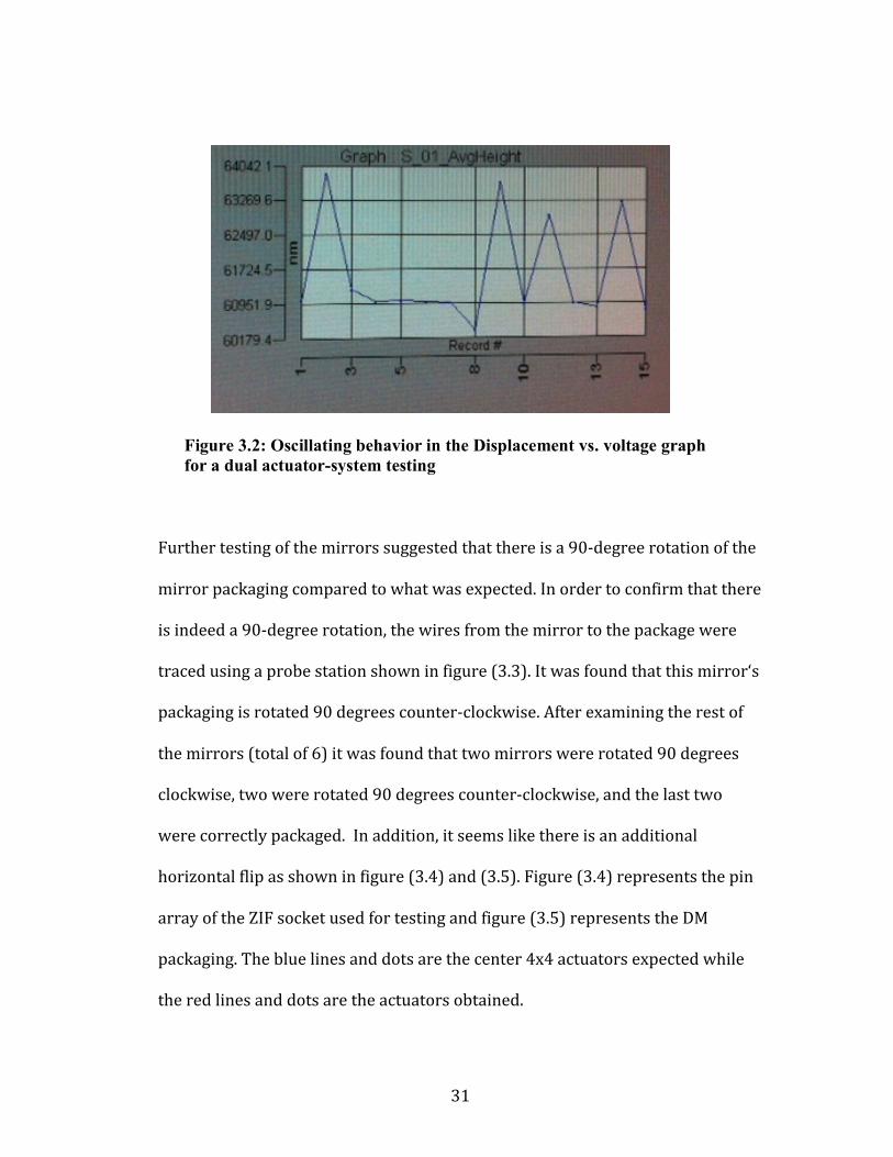
pin 1 as was requested. Another issue encountered was that applying voltage to
certain actuators showed oscillation in the displacement; they oscillated back
and forth even as the voltage increased all way up to 320 V, as shown in figure
(3.2). This result could possibly lead to the conclusion that this mirror may not
be fully released and/or the fact that there might be a humidity factor
responsible for this behavior
31
Further testing of the mirrors suggested that there is a 90-‐degree rotation of the
mirror packaging compared to what was expected. In order to confirm that there
is indeed a 90-‐degree rotation, the wires from the mirror to the package were
traced using a probe station shown in figure (3.3). It was found that this mirror‘s
packaging is rotated 90 degrees counter-‐clockwise. After examining the rest of
the mirrors (total of 6) it was found that two mirrors were rotated 90 degrees
clockwise, two were rotated 90 degrees counter-‐clockwise, and the last two
were correctly packaged. In addition, it seems like there is an additional
horizontal flip as shown in figure (3.4) and (3.5). Figure (3.4) represents the pin
array of the ZIF socket used for testing and figure (3.5) represents the DM
packaging. The blue lines and dots are the center 4x4 actuators expected while
the red lines and dots are the actuators obtained.
Figure 3.2: Oscillating behavior in the Displacement vs. voltage graph for a dual actuator-system testing

32
Figure 3.3: Probe station used for electrical and mechanical probing
Figure 3.4: ZIF socket pin array. Blue dots represent the pins wanted. Red dots represent the pins obtained
33
According to these results a new PCB was designed and sent for fabrication. The
new PCB was horizontally flipped. It was also modified by adding keep out
shapes around the voltage actuator connector and around the ground and
voltage pin as shown in figure (3.6).
Figure 3.5: DM Packaging. Blue lines represent the pins wanted. Red lines represent the pins obtained
Figure 3.6: Layout of the Horizontally flipped PCB
34
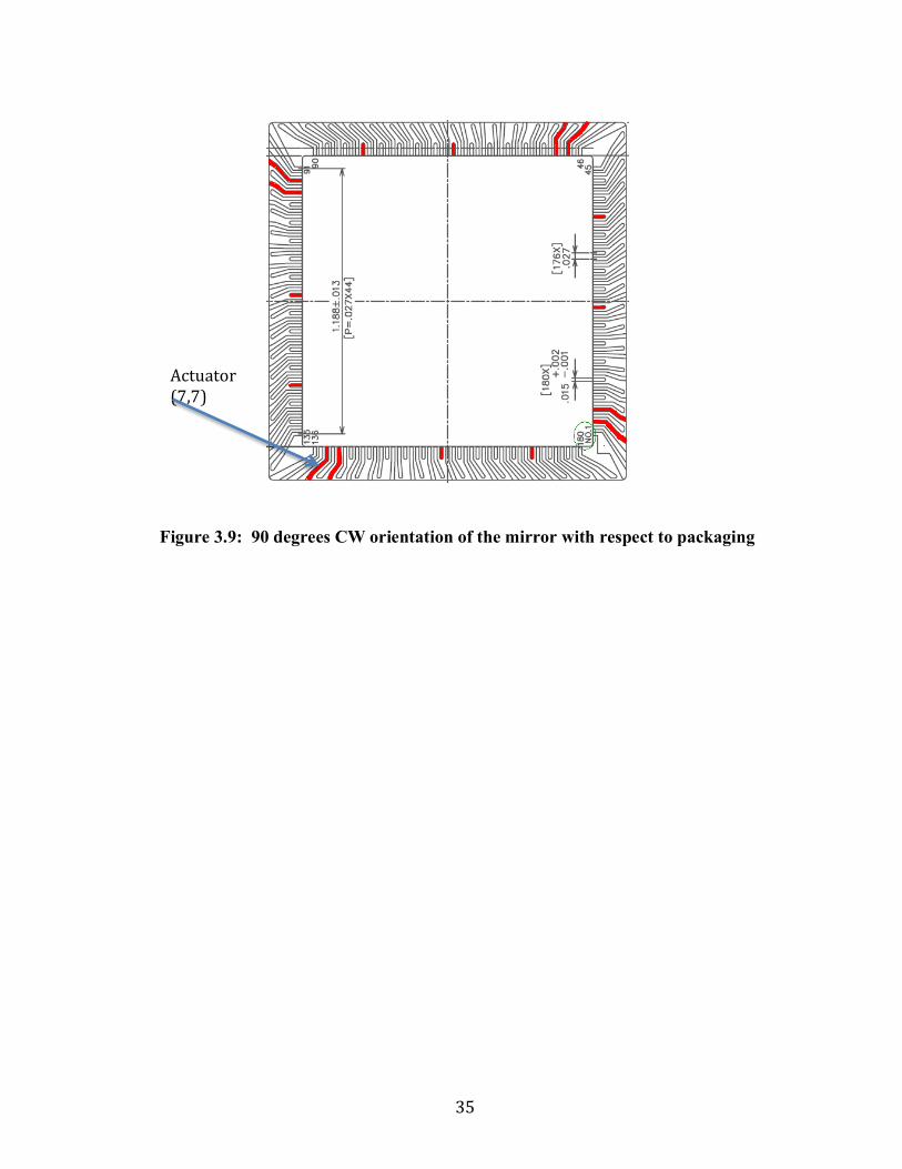
Since the PCB was flipped horizontally, the mirrors will be simply rotated either
CW or CCW and placed in the ZIF socket as shown in the following figures (3.7),
(3.8) and (3.9).
Actuator (7,7)
Figure 3.7: Correct orientation of the mirror with respect to packaging
Figure 3.8: 90 degrees CCW orientation of the mirror with respect to packaging
Actuator (7,7)
35
Figure 3.9: 90 degrees CW orientation of the mirror with respect to packaging
Actuator (7,7)
36
3.2 Results
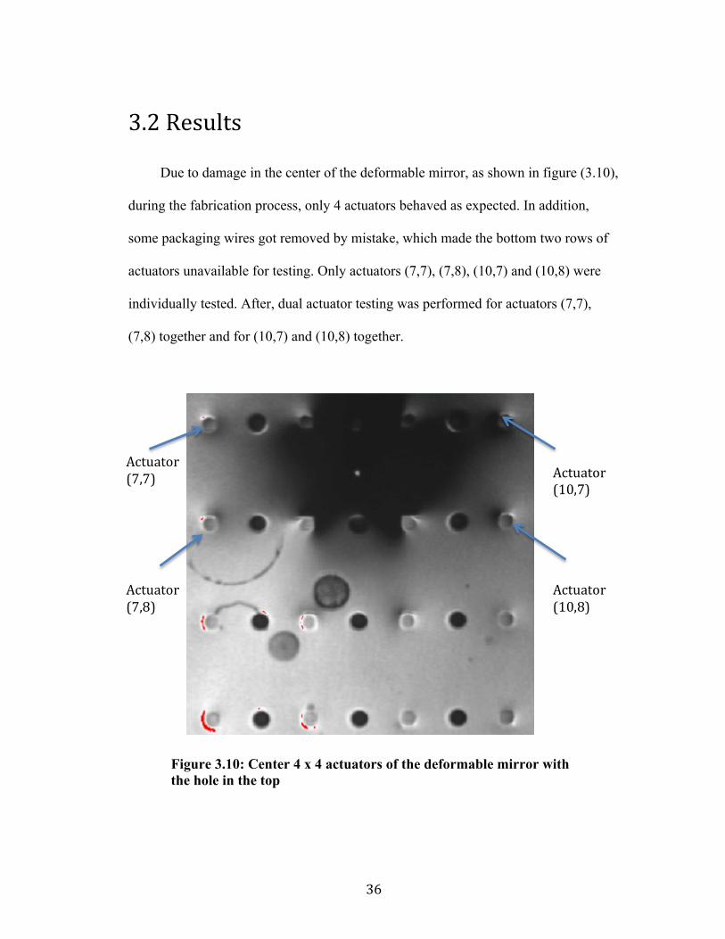
Due to damage in the center of the deformable mirror, as shown in figure (3.10),
during the fabrication process, only 4 actuators behaved as expected. In addition,
some packaging wires got removed by mistake, which made the bottom two rows of
actuators unavailable for testing. Only actuators (7,7), (7,8), (10,7) and (10,8) were
individually tested. After, dual actuator testing was performed for actuators (7,7),
(7,8) together and for (10,7) and (10,8) together.
Figure 3.10: Center 4 x 4 actuators of the deformable mirror with the hole in the top
Actuator (10,7)
Actuator (7,8)
Actuator (7,7)
Actuator (10,8)

37
3.2.1 Individual Actuator Testing
Each actuator was tested individually and displacements were recorded for
voltages from 0 - 360 V for actuator (7,7) and 0 - 380 V for actuator (10,7) and
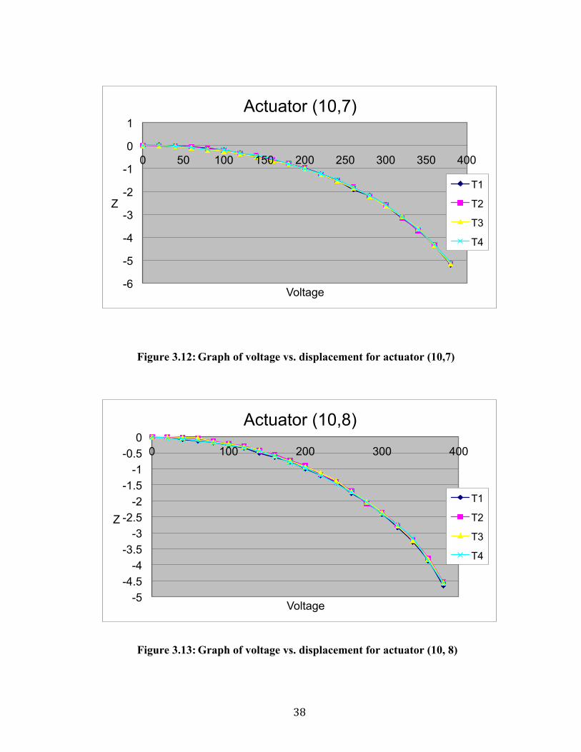
(10,8). Three trials of actuator (7,7) have been conducted leading to the graph on
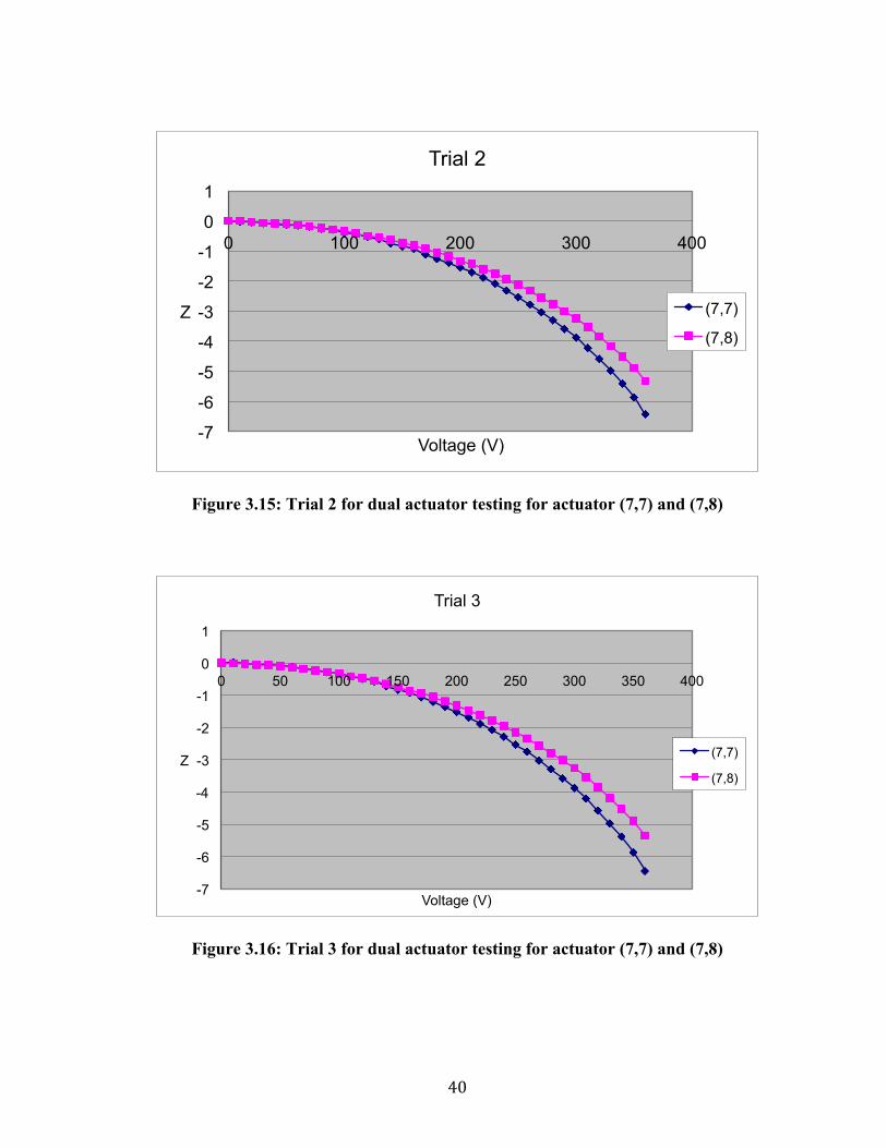
figure (3.11). While four trials of actuator (10,7) and (10,8) testing has been
conducted leading to the two graphs on figures (3.12) and (3.13), respectively. These
actuators follow the same trend that we expect; the more voltage you apply the more
displacement in the z-direction. The maximum voltage applied results in an average
displacement of 4.15 µm for actuator (7,7) at 360 V, 5.12µm for actuator (10,7) at
380 V and finally 4.58µm for actuator (10,8) at 380 V.
Figure 3.11: Graph of voltage vs. displacement for actuator (7,7)
-5
-4
-3
-2
-1
0
1
0 50 100 150 200 250 300 350 400
Z
Voltage (V)
Actuator (7,7)
T1
T2
T3
38
Figure 3.12: Graph of voltage vs. displacement for actuator (10,7)
Figure 3.13: Graph of voltage vs. displacement for actuator (10, 8)
-6
-5
-4
-3
-2
-1
0
1
0 50 100 150 200 250 300 350 400
Z
Voltage
Actuator (10,7)
T1
T2
T3
T4
-5 -4.5
-4 -3.5
-3 -2.5
-2 -1.5
-1 -0.5
0 0 100 200 300 400
Z
Voltage
Actuator (10,8)
T1
T2
T3
T4

39
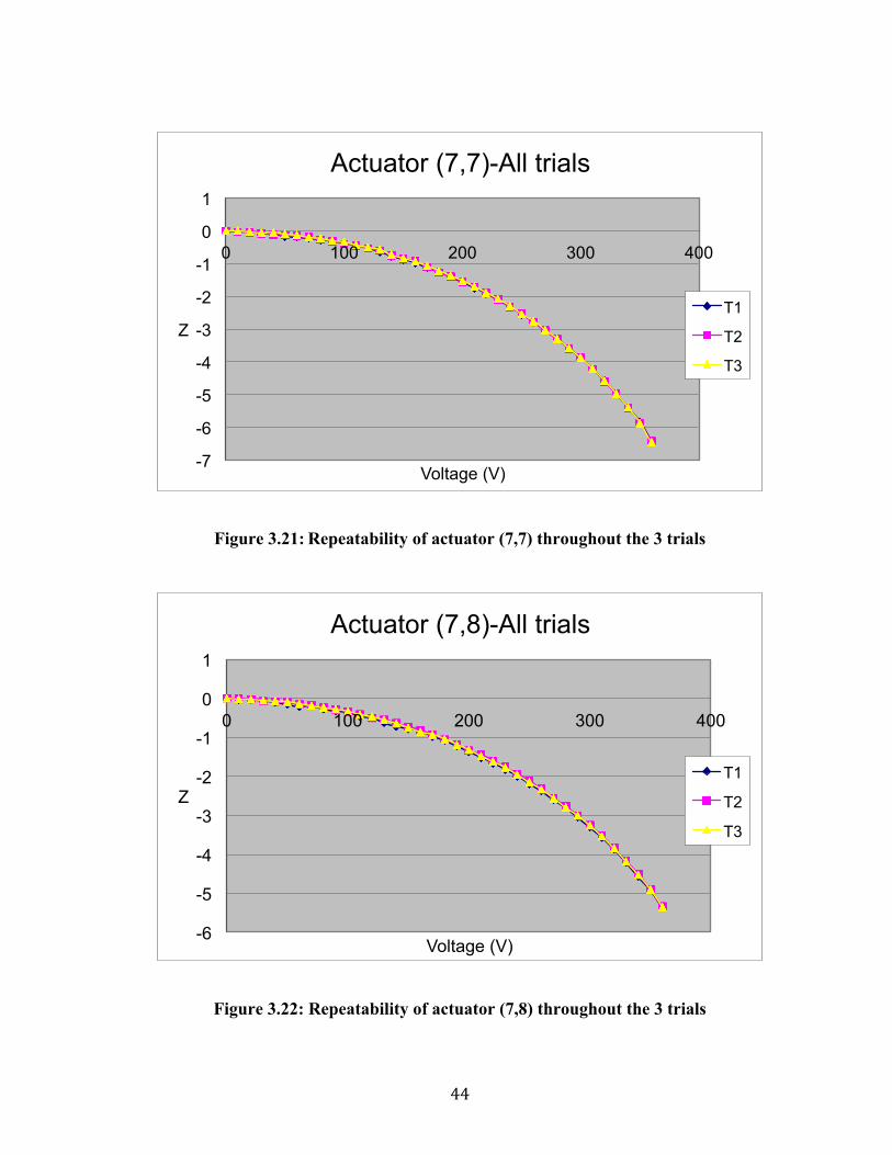
3.2.2 Two-‐Actuators Testing
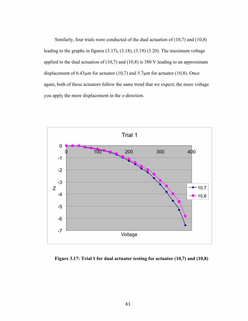
The data below represents the displacements of two neighboring actuators, (7,7)
and (7,8), being actuated at the same time under the same voltage. Three trials were
conducted leading to the graphs in figures (3.14), (3.15) and (3.16). Both of these
actuators follow the same trend that we expect; the more voltage you apply the more
displacement in the z-direction. The maximum voltage applied to the dual actuation
of (7,7) and (7,8) is 370 (V) leading approximately to a displacement of 7µm for
actuator (7,7) and 6µm for actuator (7,8).
Figure 3.14: Trial 1 for dual actuator testing for actuator (7,7) and (7,8)
-7
-6
-5
-4
-3
-2
-1
0 0 50 100 150 200 250 300 350 400
Z
Voltage (V)
Trial 1
(7,7)
(7,8)
40
Figure 3.15: Trial 2 for dual actuator testing for actuator (7,7) and (7,8)
Figure 3.16: Trial 3 for dual actuator testing for actuator (7,7) and (7,8)
-7
-6
-5
-4
-3
-2
-1
0
1
0 100 200 300 400
Z
Voltage (V)
Trial 2
(7,7)
(7,8)
-7
-6
-5
-4
-3
-2
-1
0
1
0 50 100 150 200 250 300 350 400
Z
Voltage (V)
Trial 3
(7,7)
(7,8)
41
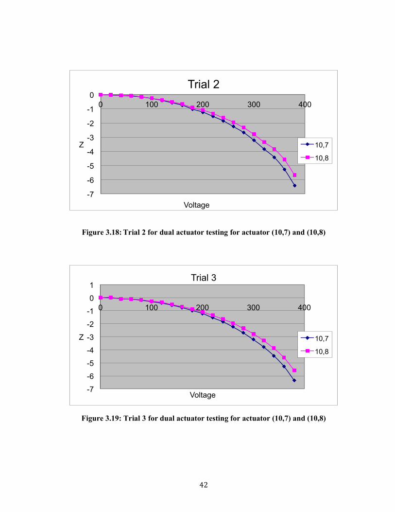
Similarly, four trials were conducted of the dual actuation of (10,7) and (10,8)
leading to the graphs in figures (3.17), (3.18), (3.19) (3.20). The maximum voltage
applied to the dual actuation of (10,7) and (10,8) is 380 V leading to an approximate
displacement of 6.43µm for actuator (10,7) and 5.7µm for actuator (10,8). Once
again, both of these actuators follow the same trend that we expect; the more voltage
you apply the more displacement in the z-direction.
-7
-6
-5
-4
-3
-2
-1
0 0 100 200 300 400
Z
Voltage
Trial 1
10,7
10,8
Figure 3.17: Trial 1 for dual actuator testing for actuator (10,7) and (10,8)
42
-7
-6
-5
-4
-3
-2
-1
0 0 100 200 300 400
Z
Voltage
Trial 2
10,7
10,8
Figure 3.18: Trial 2 for dual actuator testing for actuator (10,7) and (10,8)
-7
-6
-5
-4
-3
-2
-1
0
1
0 100 200 300 400
Z
Voltage
Trial 3
10,7
10,8
Figure 3.19: Trial 3 for dual actuator testing for actuator (10,7) and (10,8)
43
The graphs below in figures (3.21), (3.22), (3.23) and (3.24) show the
repeatability of each actuator in dual testing leading to the conclusion that these
actuators are indeed behaving as expected.
-7
-6
-5
-4
-3
-2
-1
0
1
0 100 200 300 400
Z
Voltage
Trial 4
10,7
10,8
Figure 3.20: Trial 4 for dual actuator testing for actuator (10,7) and (10,8)
44
Figure 3.21: Repeatability of actuator (7,7) throughout the 3 trials
Figure 3.22: Repeatability of actuator (7,8) throughout the 3 trials
-7
-6
-5
-4
-3
-2
-1
0
1
0 100 200 300 400
Z
Voltage (V)
Actuator (7,7)-All trials
T1
T2
T3
-6
-5
-4
-3
-2
-1
0
1
0 100 200 300 400
Z
Voltage (V)
Actuator (7,8)-All trials
T1
T2
T3

45
Figure 3.23: Repeatability of Actuator (10,7) throughout the four Trials
Figure 3.24: Repeatability of Actuator (10,8) throughout the four Trials
-7
-6
-5
-4
-3
-2
-1
0
1
0 100 200 300 400
Z
Voltage
Actuator (10,7)-All trials
T1
T2
T3
T4
-7
-6
-5
-4
-3
-2
-1
0
1
0 100 200 300 400
Z
Voltage
Actuator (10,8)-All trials
T1
T2
T3
T4
46
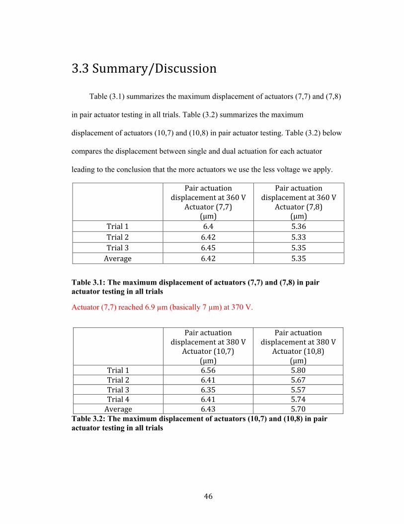
3.3 Summary/Discussion
Table (3.1) summarizes the maximum displacement of actuators (7,7) and (7,8)
in pair actuator testing in all trials. Table (3.2) summarizes the maximum
displacement of actuators (10,7) and (10,8) in pair actuator testing. Table (3.2) below
compares the displacement between single and dual actuation for each actuator
leading to the conclusion that the more actuators we use the less voltage we apply.
Pair actuation displacement at 360 V
Actuator (7,7) (µm)
Pair actuation displacement at 360 V
Actuator (7,8) (µm)
Trial 1 6.4 5.36 Trial 2 6.42 5.33 Trial 3 6.45 5.35 Average 6.42 5.35
Table 3.1: The maximum displacement of actuators (7,7) and (7,8) in pair actuator testing in all trials
Actuator (7,7) reached 6.9 µm (basically 7 µm) at 370 V.
Pair actuation displacement at 380 V
Actuator (10,7) (µm)
Pair actuation displacement at 380 V
Actuator (10,8) (µm)
Trial 1 6.56 5.80 Trial 2 6.41 5.67 Trial 3 6.35 5.57 Trial 4 6.41 5.74 Average 6.43 5.70
Table 3.2: The maximum displacement of actuators (10,7) and (10,8) in pair actuator testing in all trials
47
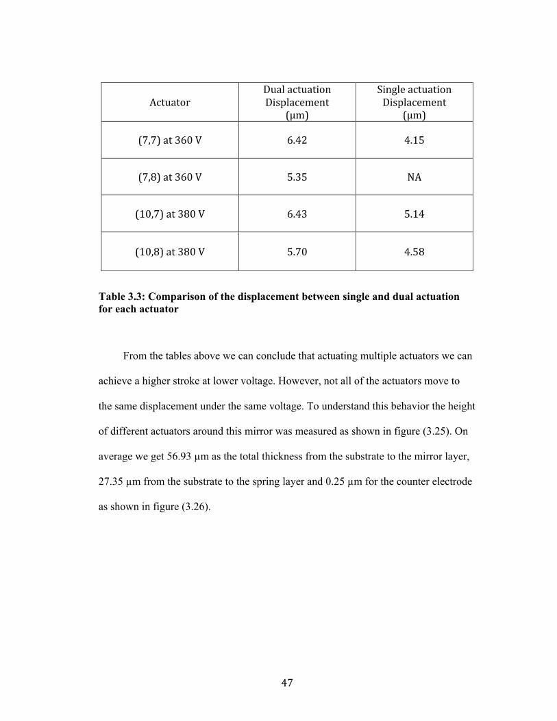
Actuator Dual actuation Displacement
(µm)
Single actuation Displacement
(µm)
(7,7) at 360 V 6.42 4.15
(7,8) at 360 V 5.35 NA
(10,7) at 380 V 6.43 5.14
(10,8) at 380 V 5.70 4.58
Table 3.3: Comparison of the displacement between single and dual actuation for each actuator
From the tables above we can conclude that actuating multiple actuators we can
achieve a higher stroke at lower voltage. However, not all of the actuators move to
the same displacement under the same voltage. To understand this behavior the height
of different actuators around this mirror was measured as shown in figure (3.25). On
average we get 56.93 µm as the total thickness from the substrate to the mirror layer,
27.35 µm from the substrate to the spring layer and 0.25 µm for the counter electrode
as shown in figure (3.26).
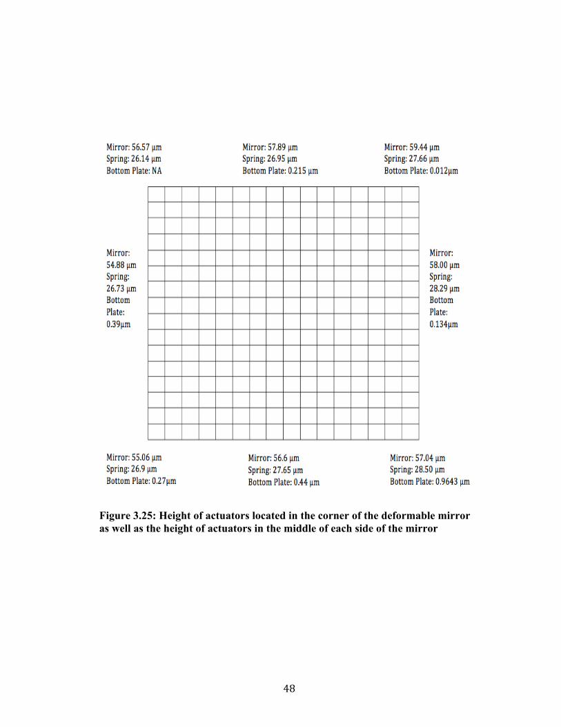
48
Figure 3.25: Height of actuators located in the corner of the deformable mirror as well as the height of actuators in the middle of each side of the mirror

49
Figure 3.26: Average height from the substrate to the mirror layer, from the substrate to the spring layer and for the counter electrode of this deformable mirror
There are also bulls-eye test structures, as shown on figure (3.27), on two sides of this
mirror: the right side and the bottom side. The heights of different layers of the bulls-
eye were measured and summarized in table (3.4) below. On average, we get 0.44 µm
for counter electrode, 22.493 µm for the gap between the counter electrode and the
spring layer, 5.882 µm for spring layer, 25.3 µm for the post gap and 3.7 µm for the
mirror layer leading to a total of 57.82 µm from the substrate to the mirror layer.

50
Location Counter electrode Gap Spring
layer Post Gap Mirror Total
Right 1 0.47 22.49 6.31 24.28 5.94 59.48 Right 2 0.44 22.51 4.81 27.01 2.44 57.22 Right 3 0.36 22.65 5.57 28.25 1.35 58.19 Right 4 0.44 22.57 5.73 27.06 3.53 59.31 Right 5 0.42 22.66 5.74 24.92 3.46 57.20 Right 6 0.46 22.64 6.02 20.75 7.42 57.29 Right 7 0.48 22.57 5.72 27.39 1.10 57.27
Bottom 1 0.49 22.60 7.12 24.59 2.56 57.35 Bottom 2 0.41 22.51 5.25 26.87 2.44 57.49 Bottom 3 0.44 22.39 6.44 23.80 3.96 57.03 Bottom 4 0.45 22.27 5.36 25.82 5.80 59.70 Bottom 5 0.42 22.06 6.51 22.90 4.38 56.27 Average 0.44 22.49 5.88 25.30 3.70 57.82
Table 3.4: Summary of the heights of the counter electrode, the gap between the counter electrode and spring layer, the post gap, the mirror layer and the total height of each bulls-eye that are part of the DM.
Figure 3.27: An illustration of a test-structure (bulls-eye) found around the mirror
51
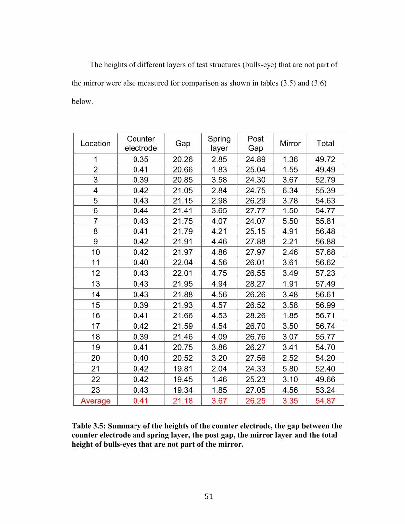
The heights of different layers of test structures (bulls-eye) that are not part of
the mirror were also measured for comparison as shown in tables (3.5) and (3.6)
below.
Location Counter electrode Gap Spring
layer Post Gap Mirror Total
1 0.35 20.26 2.85 24.89 1.36 49.72 2 0.41 20.66 1.83 25.04 1.55 49.49 3 0.39 20.85 3.58 24.30 3.67 52.79 4 0.42 21.05 2.84 24.75 6.34 55.39 5 0.43 21.15 2.98 26.29 3.78 54.63 6 0.44 21.41 3.65 27.77 1.50 54.77 7 0.43 21.75 4.07 24.07 5.50 55.81 8 0.41 21.79 4.21 25.15 4.91 56.48 9 0.42 21.91 4.46 27.88 2.21 56.88
10 0.42 21.97 4.86 27.97 2.46 57.68 11 0.40 22.04 4.56 26.01 3.61 56.62 12 0.43 22.01 4.75 26.55 3.49 57.23 13 0.43 21.95 4.94 28.27 1.91 57.49 14 0.43 21.88 4.56 26.26 3.48 56.61 15 0.39 21.93 4.57 26.52 3.58 56.99 16 0.41 21.66 4.53 28.26 1.85 56.71 17 0.42 21.59 4.54 26.70 3.50 56.74 18 0.39 21.46 4.09 26.76 3.07 55.77 19 0.41 20.75 3.86 26.27 3.41 54.70 20 0.40 20.52 3.20 27.56 2.52 54.20 21 0.42 19.81 2.04 24.33 5.80 52.40 22 0.42 19.45 1.46 25.23 3.10 49.66 23 0.43 19.34 1.85 27.05 4.56 53.24
Average 0.41 21.18 3.67 26.25 3.35 54.87
Table 3.5: Summary of the heights of the counter electrode, the gap between the counter electrode and spring layer, the post gap, the mirror layer and the total height of bulls-eyes that are not part of the mirror.
52
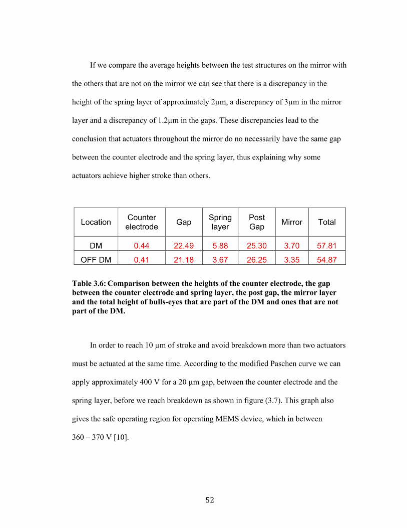
If we compare the average heights between the test structures on the mirror with
the others that are not on the mirror we can see that there is a discrepancy in the
height of the spring layer of approximately 2µm, a discrepancy of 3µm in the mirror
layer and a discrepancy of 1.2µm in the gaps. These discrepancies lead to the
conclusion that actuators throughout the mirror do no necessarily have the same gap
between the counter electrode and the spring layer, thus explaining why some
actuators achieve higher stroke than others.
Location Counter electrode Gap Spring
layer Post Gap Mirror Total
DM 0.44 22.49 5.88 25.30 3.70 57.81
OFF DM 0.41 21.18 3.67 26.25 3.35 54.87
Table 3.6: Comparison between the heights of the counter electrode, the gap between the counter electrode and spring layer, the post gap, the mirror layer and the total height of bulls-eyes that are part of the DM and ones that are not part of the DM.
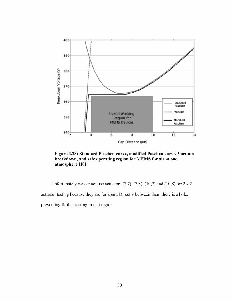
In order to reach 10 µm of stroke and avoid breakdown more than two actuators
must be actuated at the same time. According to the modified Paschen curve we can
apply approximately 400 V for a 20 µm gap, between the counter electrode and the
spring layer, before we reach breakdown as shown in figure (3.7). This graph also
gives the safe operating region for operating MEMS device, which in between
360 – 370 V [10].
53
Figure 3.28: Standard Paschen curve, modified Paschen curve, Vacuum breakdown, and safe operating region for MEMS for air at one atmosphere [10]
Unfortunately we cannot use actuators (7,7), (7,8), (10,7) and (10,8) for 2 x 2
actuator testing because they are far apart. Directly between them there is a hole,
preventing further testing in that region.

54
Chapter 4: Future Work
4.1 Individual Actuator Testing
In order to perform 2 x 2 testing, a second 16 x 16 X-beam actuators deformable
mirror is in the process of being tested. Figure (4.1) shows an image of the center 4 x
4 actuators of this mirror. A displacement of 1.4 µm on average is achieved at a
maximum voltage of 280 V. This displacement is basically 1 µm less than the
previous mirror discussed above in this thesis at the same voltage. Preliminary
individual testing of the 16 x 16 X-beam deformable mirror showed that 13 out of the
16 4 x 4 center actuators are more or less behaving as expected. The graphs below
show the average displacement of each actuator from 0 to 280 V for 13 actuators of
the center 4 x 4 as shown in figures (4.2), (4.3), (4.4) and (4.5). We can therefore
conduct dual, 2 x 2 and eventually 4 x 4 testing and see how much displacement we
can achieve.
Figure 4.1: Image of the Center 4 x 4 X-Beam Actuators of second DM
55
Figure 4.2: Graph of the average displacement of actuator (7,7), (8,7) and (10,7) from 0 to 280 V for the top row of the center 4 x 4
Figure 4.3: Graph of the average displacement of actuator (8,8), (9,8) and (10,8) from 0 to 280 V for the second row of the center 4 x 4
-1.6
-1.4
-1.2
-1
-0.8
-0.6
-0.4
-0.2
0
0.2
0 50 100 150 200 250 300
Z
Volatge (V)
Average of three trials of each actuator
(7,7)
(8,7)
(10,7)
-1.6
-1.4
-1.2
-1
-0.8
-0.6
-0.4
-0.2
0
0.2
0 50 100 150 200 250 300
Z
Volatge (V)
Average Three Trials of Each Actuator
(8,8)
(9,8)
(10,8)
56
Figure 4.4: Graph of the average displacement of actuator (7,9), (8,9), (9,9) and (10,9) from 0 to 280 V for the third row of the center 4 x 4
Figure 4.5: Graph of the average displacement of actuator (7,10), (8,10), and (9,10) from 0 to 280 V for the bottom row of the center 4 x 4
-1.6
-1.4
-1.2
-1
-0.8
-0.6
-0.4
-0.2
0
0.2
0 50 100 150 200 250 300
Z
Voltage (V)
Average Three Trials of Each Actuator
(8,9)
(9,9)
(10,9)
(7,9)
-1.6
-1.4
-1.2
-1
-0.8
-0.6
-0.4
-0.2
0
0.2
0 50 100 150 200 250 300
Z
Voltage
Average Three Trials of Each Actuator
(7,10)
(8,10)
(9,10)

57
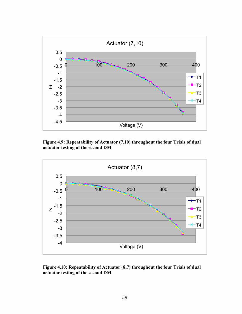
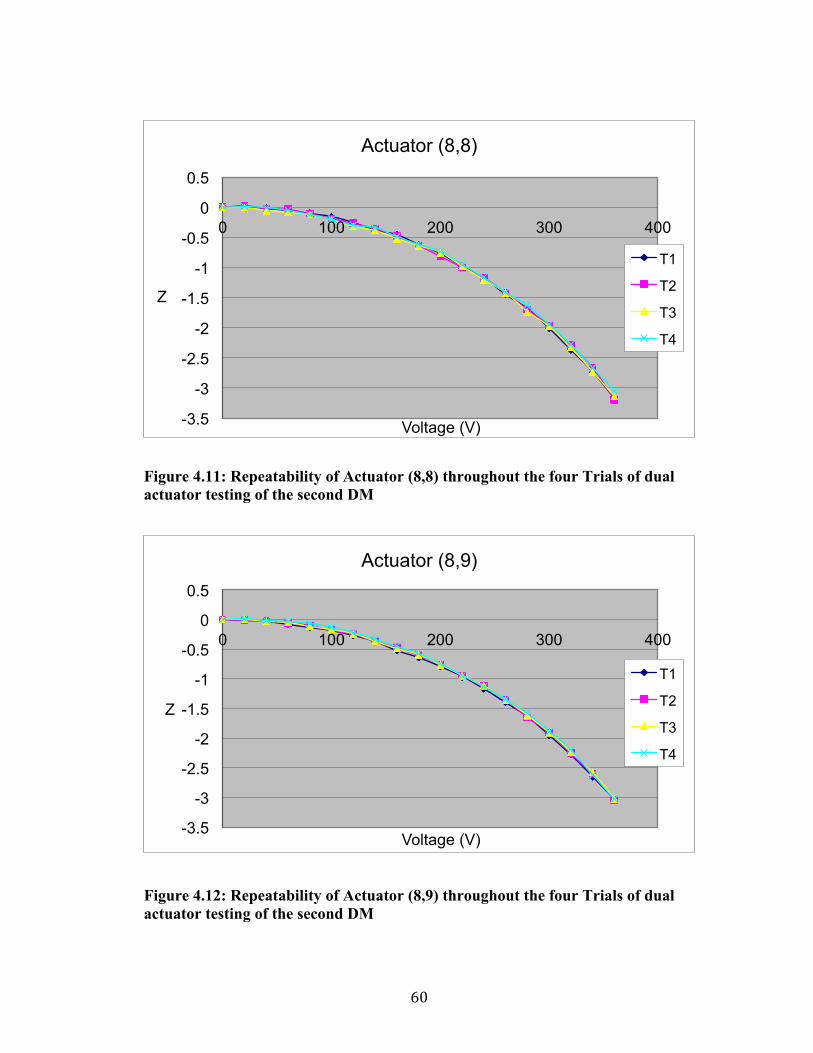
4.2 Dual Actuators Testing
The second mirror’s dual testing have shown that the center 4 x 4 x-beam actuators
are behaving as expected; the more voltage applied the more displacement achieved
as shown in the figures below. Also, these results show that the more actuators are
tested at the same time the less voltage applied, which is similar to the behavior of the
first DM tested. In addition, this graphs show that the behavior of these actuators is
also repeatable in the four trials conducted for each actuator. However, the maximum
displacement achieved in dual actuator testing is only 4.5µm at 360 V for actuator
(7,7) compared to the same actuator of the first mirror.
Figure 4.6: Repeatability of Actuator (7,7) throughout the four Trials of dual actuator testing of the second DM
-5 -4.5
-4 -3.5
-3 -2.5
-2 -1.5
-1 -0.5
0 0.5
0 100 200 300 400
Z
Voltage (V)
Actuator (7,7)
Series1
Series2
Series3
Series4

58
Figure 4.7: Repeatability of Actuator (7,8) throughout the four Trials of dual actuator testing of the second DM
Figure 4.8: Repeatability of Actuator (7,9) throughout the four Trials of dual actuator testing of the second DM
-4.5 -4
-3.5 -3
-2.5 -2
-1.5 -1
-0.5 0
0.5
0 100 200 300 400
Z
Voltage (V)
Acuator (7,8)
Series1
Series2
Series3
Series4
-4 -3.5
-3 -2.5
-2 -1.5
-1 -0.5
0 0.5
0 100 200 300 400
Z
Voltage (V)
Actuator (7,9)
T1
T2
T3
T4
59
Figure 4.9: Repeatability of Actuator (7,10) throughout the four Trials of dual actuator testing of the second DM
Figure 4.10: Repeatability of Actuator (8,7) throughout the four Trials of dual actuator testing of the second DM
-4.5 -4
-3.5 -3
-2.5 -2
-1.5 -1
-0.5 0
0.5
0 100 200 300 400
Z
Voltage (V)
Actuator (7,10)
T1
T2
T3
T4
-4 -3.5
-3 -2.5
-2 -1.5
-1 -0.5
0 0.5
0 100 200 300 400
Z
Voltage (V)
Actuator (8,7)
T1
T2
T3
T4
60
Figure 4.11: Repeatability of Actuator (8,8) throughout the four Trials of dual actuator testing of the second DM
Figure 4.12: Repeatability of Actuator (8,9) throughout the four Trials of dual actuator testing of the second DM
-3.5
-3
-2.5
-2
-1.5
-1
-0.5
0
0.5
0 100 200 300 400
Z
Voltage (V)
Actuator (8,8)
T1
T2
T3
T4
-3.5
-3
-2.5
-2
-1.5
-1
-0.5
0
0.5
0 100 200 300 400
Z
Voltage (V)
Actuator (8,9)
T1
T2
T3
T4
61
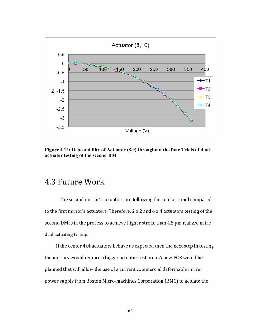
Figure 4.13: Repeatability of Actuator (8,9) throughout the four Trials of dual actuator testing of the second DM
4.3 Future Work
The second mirror’s actuators are following the similar trend compared
to the first mirror’s actuators. Therefore, 2 x 2 and 4 x 4 actuators testing of the
second DM is in the process to achieve higher stroke than 4.5 µm realized in the
dual actuating testing.
If the center 4x4 actuators behave as expected then the next step in testing
the mirrors would require a bigger actuator test area. A new PCB would be
planned that will allow the use of a current commercial deformable mirror
power supply from Boston Micro-‐machines Corporation (BMC) to actuate the
-3.5
-3
-2.5
-2
-1.5
-1
-0.5
0
0.5
0 50 100 150 200 250 300 350 400
Z
Voltage (V)
Actuator (8,10)
T1
T2
T3
T4
62
deformable mirrors actuators at different voltages. The voltage output of the
BMC power supply will be summed to a constant voltage to allow a high voltage
(+300V) to be applied to each actuator. The testing will be performed on the
central 4×4 and eventually expanded to the entire central 12×12 actuators.

63
Conclusion
Micro-Electro-Mechanical System (MEMS) X-beam actuators deformable
mirrors were fabricated using high-aspect ratio monolithic process by Innovative
Micro Technology. This process was used to fabricate 16 x 16 X-beam actuators
deformable mirrors and individual and dual actuator testing has been conducted.
Thorough characterization testing was performed on the fabricated MEMS
deformable mirrors. The Veeco WYKO NT1100 White Light Interferometer was
used to perform stroke measurements while the data was collected in the WYKO
Vision 32 Software for further analysis.
Single actuator testing achieved approximately a maximum of 5.14µm for
actuator (10,7) while dual actuator testing achieved a maximum of approximately
7µm for actuator (7,7) for the first deformable mirror. These results show that
applying voltage to multiple actuators achieves a higher stroke at lower voltage. In
addition, the data show the repeatability of these actuators’ voltage vs. displacement
curve as expected.
These results lead to the conclusion that the high aspect ratio monolithic
fabrication process is capable of the fabrication of high stroke MEMS deformable
mirrors that are suitable for the next generation of telescopes. In addition, these
mirrors hold great promise for applications in vision science that requires a stroke of
15 µm.

64
Bibliography
1) Dr. Claire Max, Center for Adaptive Optics, University of California, Santa Cruz
2) Thomas Bifano, Paul Bierden, and Julie Perreault, Micromachined Deformable Mirrors for Dynamic Wavefront Control, Proc. SPIE 5553, pp. 10-‐13 (2004).
3) Joel A. Kubby, A Guide to Hands-on MEMS Design and Prototyping,
Cambridge University Press, (2011).
4) Joel Kubby, Adaptive Optics for Biological Imaging, Taylor & Francis, CRC Press.
5) Bautista R. Fernández and Joel Kubby, High-aspect ratio microelectromechanical systems deformable mirrors for adaptive optics, J. Micro/Nanolitho. MEMS MOEMS 9, pp. 041106 (2010).
6) Bautista Fernández Rocha, Design, Fabrication and Characterization of High-Stroke High-Aspect Ratio Micro Electro Mechanical Systems Deformable Mirrors For Adaptive Optics, PhD Thesis, University of California Santa Cruz, Dept. of Electrical Engineering (2011).
7) E. S. Hung and S. D. Senturia, “Extending the travel range of analog tuned electrostatic actuators,” Journal of Microelectromechanical Systems 8, 497–505 (1999).
8) Veeco. "NT1100 Setup Guide".
9) Geoff Andersen, The Telescope-‐ Its History, Technology, and Future, Princeton University Press, New Jersey, pp 44 – 139 (2006).
10) Allyson L. Hartzell , Herbert R. Shea , MEMS Reliability, Springer, (2011)