Embed Size (px)
Citation preview
Important notice Dear Customer, On 7 February 2017 the former NXP Standard Product business became a new company with the tradename Nexperia. Nexperia is an industry leading supplier of Discrete, Logic and PowerMOS semiconductors with its focus on the automotive, industrial, computing, consumer and wearable application markets In data sheets and application notes which still contain NXP or Philips Semiconductors references, use the references to Nexperia, as shown below. Instead of http://www.nxp.com, http://www.philips.com/ or http://www.semiconductors.philips.com/, use http://www.nexperia.com Instead of [email protected] or [email protected], use [email protected] (email) Replace the copyright notice at the bottom of each page or elsewhere in the document, depending on the version, as shown below: - © NXP N.V. (year). All rights reserved or © Koninklijke Philips Electronics N.V. (year). All rights reserved Should be replaced with: - © Nexperia B.V. (year). All rights reserved. If you have any questions related to the data sheet, please contact our nearest sales office via e-mail or telephone (details via [email protected]). Thank you for your cooperation and understanding,
Kind regards,
Team Nexperia
DATA SHEET
Product data sheet Supersedes data of 2004 Apr 06
2004 Aug 06
DISCRETE SEMICONDUCTORS
PDTC115E seriesNPN resistor-equipped transistors; R1 = 100 kΩ, R2 = 100 kΩ
NXP Semiconductors Product data sheet
NPN resistor-equipped transistors; R1 = 100 kΩ, R2 = 100 kΩ
PDTC115E series
FEATURES
• Built-in bias resistors• Simplified circuit design• Reduction of component count• Reduced pick and place costs.
APPLICATIONS
• General purpose switching and amplification• Inverter and interface circuits• Circuit driver.
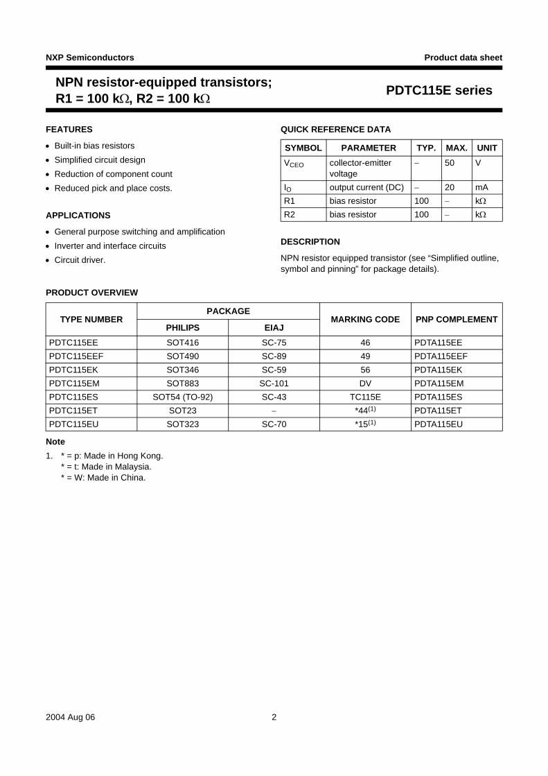
QUICK REFERENCE DATA
DESCRIPTION
NPN resistor equipped transistor (see “Simplified outline, symbol and pinning” for package details).
SYMBOL PARAMETER TYP. MAX. UNITVCEO collector-emitter
voltage− 50 V
IO output current (DC) − 20 mAR1 bias resistor 100 − kΩ
R2 bias resistor 100 − kΩ
PRODUCT OVERVIEW
Note1. * = p: Made in Hong Kong.
* = t: Made in Malaysia. * = W: Made in China.
TYPE NUMBERPACKAGE
MARKING CODE PNP COMPLEMENTPHILIPS EIAJ
PDTC115EE SOT416 SC-75 46 PDTA115EEPDTC115EEF SOT490 SC-89 49 PDTA115EEFPDTC115EK SOT346 SC-59 56 PDTA115EKPDTC115EM SOT883 SC-101 DV PDTA115EMPDTC115ES SOT54 (TO-92) SC-43 TC115E PDTA115ESPDTC115ET SOT23 − *44(1) PDTA115ETPDTC115EU SOT323 SC-70 *15(1) PDTA115EU
2004 Aug 06 2
NXP Semiconductors Product data sheet
NPN resistor-equipped transistors; R1 = 100 kΩ, R2 = 100 kΩ
PDTC115E series
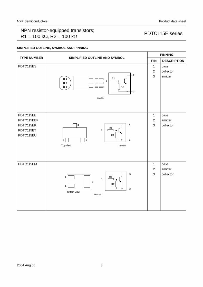
SIMPLIFIED OUTLINE, SYMBOL AND PINNING
TYPE NUMBER SIMPLIFIED OUTLINE AND SYMBOLPINNING
PIN DESCRIPTIONPDTC115ES 1 base
2 collector3 emitter
PDTC115EE 1 basePDTC115EEF 2 emitterPDTC115EK 3 collectorPDTC115ETPDTC115EU
PDTC115EM 1 base2 emitter3 collector
handbook, halfpage
MAM364
1
2
3
R1
R2
2
3
1
handbook, halfpage
MDB269
1
2
3
Top view
R1
R2
1 2
3
handbook, halfpage
MHC506
1
2
3R1
R2
2
1
3
bottom view
2004 Aug 06 3
NXP Semiconductors Product data sheet
NPN resistor-equipped transistors; R1 = 100 kΩ, R2 = 100 kΩ
PDTC115E series
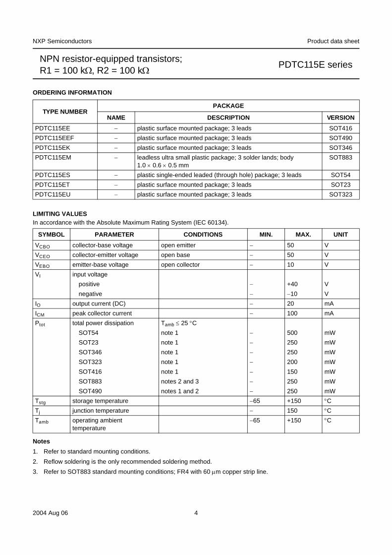
ORDERING INFORMATION
LIMITING VALUESIn accordance with the Absolute Maximum Rating System (IEC 60134).
Notes1. Refer to standard mounting conditions.2. Reflow soldering is the only recommended soldering method.3. Refer to SOT883 standard mounting conditions; FR4 with 60 μm copper strip line.
TYPE NUMBERPACKAGE
NAME DESCRIPTION VERSIONPDTC115EE − plastic surface mounted package; 3 leads SOT416PDTC115EEF − plastic surface mounted package; 3 leads SOT490PDTC115EK − plastic surface mounted package; 3 leads SOT346PDTC115EM − leadless ultra small plastic package; 3 solder lands; body
1.0 × 0.6 × 0.5 mmSOT883
PDTC115ES − plastic single-ended leaded (through hole) package; 3 leads SOT54PDTC115ET − plastic surface mounted package; 3 leads SOT23PDTC115EU − plastic surface mounted package; 3 leads SOT323
SYMBOL PARAMETER CONDITIONS MIN. MAX. UNITVCBO collector-base voltage open emitter − 50 VVCEO collector-emitter voltage open base − 50 VVEBO emitter-base voltage open collector − 10 VVI input voltage
positive − +40 Vnegative − −10 V
IO output current (DC) − 20 mAICM peak collector current − 100 mAPtot total power dissipation Tamb ≤ 25 °C
SOT54 note 1 − 500 mWSOT23 note 1 − 250 mWSOT346 note 1 − 250 mWSOT323 note 1 − 200 mWSOT416 note 1 − 150 mWSOT883 notes 2 and 3 − 250 mWSOT490 notes 1 and 2 − 250 mW
Tstg storage temperature −65 +150 °CTj junction temperature − 150 °CTamb operating ambient
temperature−65 +150 °C
2004 Aug 06 4
NXP Semiconductors Product data sheet
NPN resistor-equipped transistors; R1 = 100 kΩ, R2 = 100 kΩ
PDTC115E series
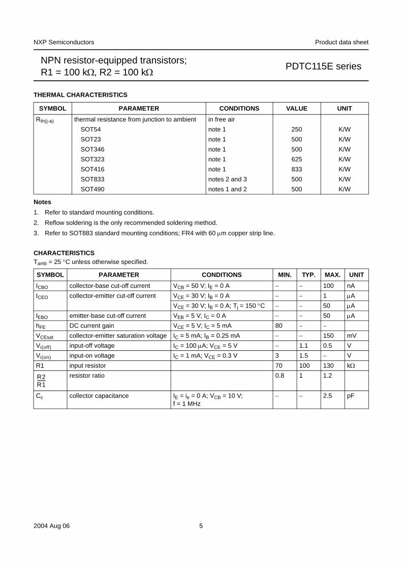
THERMAL CHARACTERISTICS
Notes1. Refer to standard mounting conditions.2. Reflow soldering is the only recommended soldering method.3. Refer to SOT883 standard mounting conditions; FR4 with 60 μm copper strip line.
CHARACTERISTICSTamb = 25 °C unless otherwise specified.
SYMBOL PARAMETER CONDITIONS VALUE UNITRth(j-a) thermal resistance from junction to ambient in free air
SOT54 note 1 250 K/WSOT23 note 1 500 K/WSOT346 note 1 500 K/WSOT323 note 1 625 K/WSOT416 note 1 833 K/WSOT833 notes 2 and 3 500 K/WSOT490 notes 1 and 2 500 K/W
SYMBOL PARAMETER CONDITIONS MIN. TYP. MAX. UNITICBO collector-base cut-off current VCB = 50 V; IE = 0 A − − 100 nAICEO collector-emitter cut-off current VCE = 30 V; IB = 0 A − − 1 μA
VCE = 30 V; IB = 0 A; Tj = 150 °C − − 50 μAIEBO emitter-base cut-off current VEB = 5 V; IC = 0 A − − 50 μAhFE DC current gain VCE = 5 V; IC = 5 mA 80 − −
VCEsat collector-emitter saturation voltage IC = 5 mA; IB = 0.25 mA − − 150 mVVi(off) input-off voltage IC = 100 μA; VCE = 5 V − 1.1 0.5 VVi(on) input-on voltage IC = 1 mA; VCE = 0.3 V 3 1.5 − VR1 input resistor 70 100 130 kΩ
resistor ratio 0.8 1 1.2
Cc collector capacitance IE = ie = 0 A; VCB = 10 V; f = 1 MHz
− − 2.5 pF
R2R1--------
2004 Aug 06 5
NXP Semiconductors Product data sheet
NPN resistor-equipped transistors; R1 = 100 kΩ, R2 = 100 kΩ
PDTC115E series
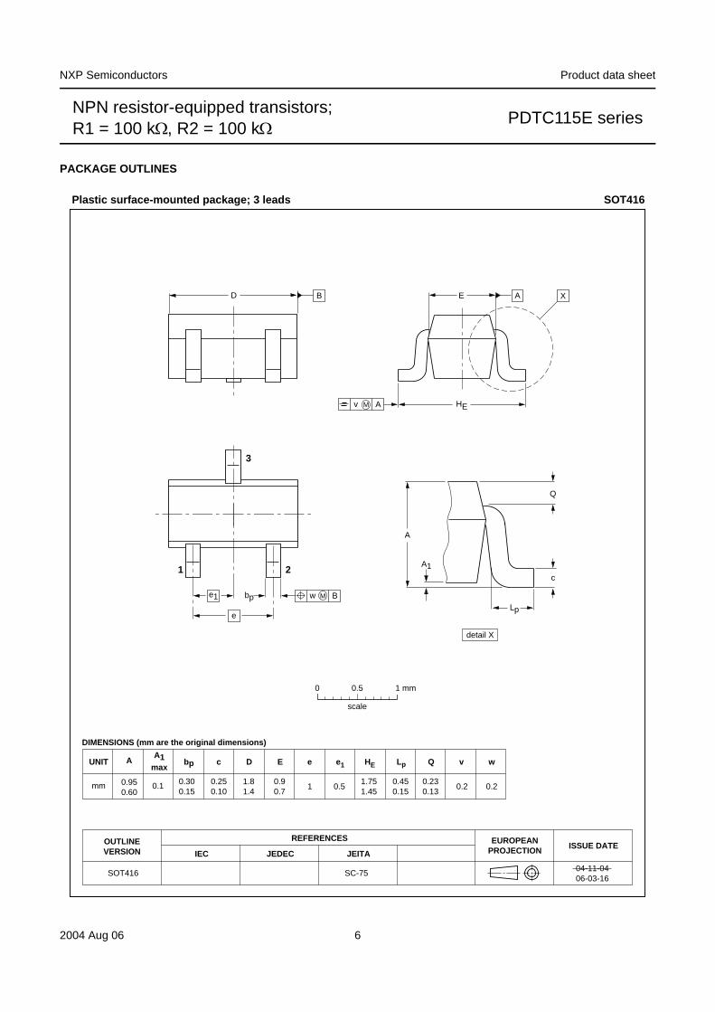
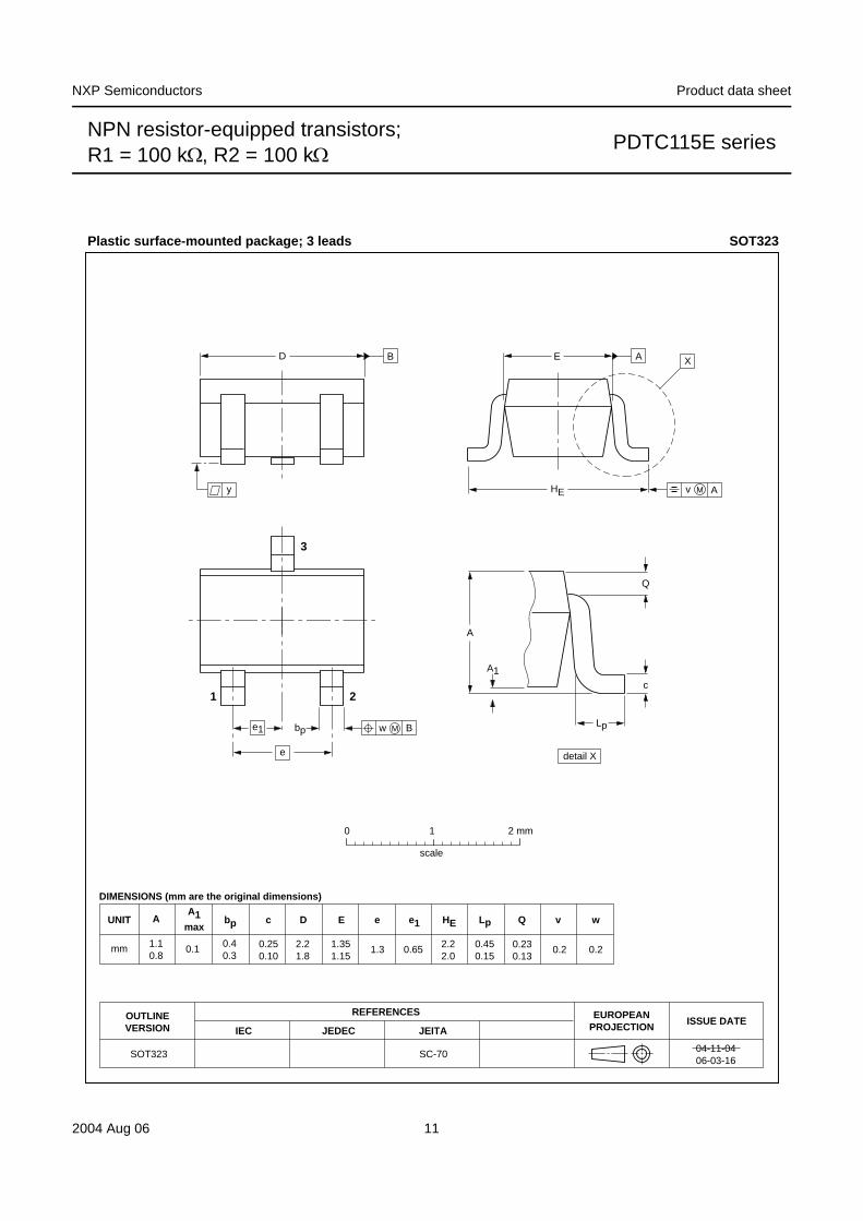
PACKAGE OUTLINES
UNITA1
maxbp c D E e1 HE Lp Q w
REFERENCESOUTLINEVERSION
EUROPEANPROJECTION ISSUE DATE
IEC JEDEC JEITA
mm 0.1 0.300.15
0.250.10
1.81.4
0.90.7
0.5
e
11.751.45
0.2
v
0.2
DIMENSIONS (mm are the original dimensions)
0.450.15
0.230.13
SOT416 SC-75
w Mbp
D
e1
e
A
A1
Lp
Q
detail X
HE
E AB
B
v M A
0 0.5 1 mm
scale
A
0.950.60
c
X
1 2
3
Plastic surface-mounted package; 3 leads SOT416
04-11-0406-03-16
2004 Aug 06 6

NXP Semiconductors Product data sheet
NPN resistor-equipped transistors; R1 = 100 kΩ, R2 = 100 kΩ
PDTC115E series
UNIT A1 bp c D E e1 HE Lp Q wv
REFERENCESOUTLINEVERSION
EUROPEANPROJECTION ISSUE DATE
IEC JEDEC JEITA
mm 0.500.35
0.260.10
3.12.7
1.71.3
0.95
e
1.9 3.02.5
0.330.23
0.20.2
DIMENSIONS (mm are the original dimensions)
0.60.2
SOT346 TO-236 SC-59A
bp
D
e1
e
A
A1
Lp
Q
detail X
HE
E
w M
v M A
B
A
B
0 1 2 mm
scale
A
1.31.0
0.10.013
c
X
1 2
3
Plastic surface-mounted package; 3 leads SOT346
04-11-1106-03-16
2004 Aug 06 7
NXP Semiconductors Product data sheet
NPN resistor-equipped transistors; R1 = 100 kΩ, R2 = 100 kΩ
PDTC115E series
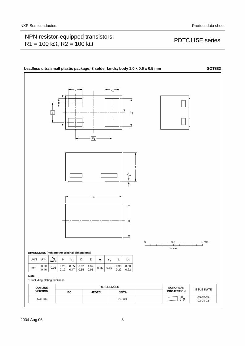
UNITA1
max.A(1) b b1 e1e L L1
REFERENCESOUTLINEVERSION
EUROPEANPROJECTION ISSUE DATE
IEC JEDEC JEITA
mm 0.500.46
0.200.12
0.550.47
0.03 0.620.55
0.35 0.65
DIMENSIONS (mm are the original dimensions)
Note
1. Including plating thickness
0.300.22
0.300.22
SOT883 SC-101 03-02-0503-04-03
D E
1.020.95
L
E
2
3
1
b
b1
A1
A
D
L1
0 0.5 1 mm
scale
Leadless ultra small plastic package; 3 solder lands; body 1.0 x 0.6 x 0.5 mm SOT883
e
e1
2004 Aug 06 8
NXP Semiconductors Product data sheet
NPN resistor-equipped transistors; R1 = 100 kΩ, R2 = 100 kΩ
PDTC115E series
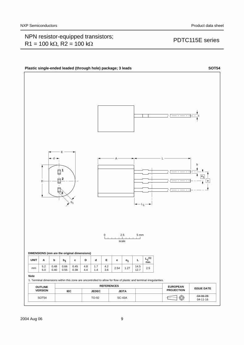
UNIT A
REFERENCESOUTLINEVERSION
EUROPEANPROJECTION ISSUE DATE
IEC JEDEC JEITA
mm5.25.0
b
0.480.40
c
0.450.38
D
4.84.4
d
1.71.4
E
4.23.6
L
14.512.7
e
2.54
e1
1.27
L1(1)
max.
2.5
b1
0.660.55
DIMENSIONS (mm are the original dimensions)
Note
1. Terminal dimensions within this zone are uncontrolled to allow for flow of plastic and terminal irregularities.
SOT54 TO-92 SC-43A04-06-2804-11-16
A L
0 2.5 5 mm
scale
b
c
D
b1 L1
d
E
Plastic single-ended leaded (through hole) package; 3 leads SOT54
e1e
1
2
3
2004 Aug 06 9
NXP Semiconductors Product data sheet
NPN resistor-equipped transistors; R1 = 100 kΩ, R2 = 100 kΩ
PDTC115E series
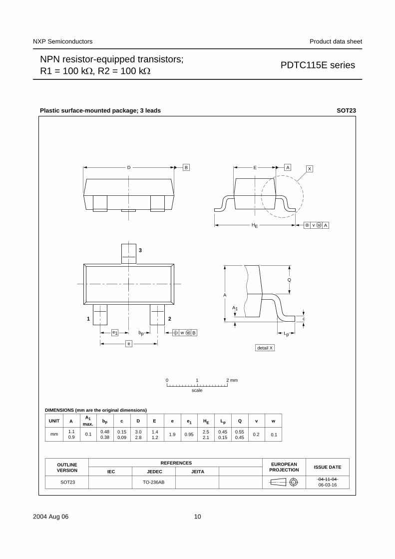
UNITA1
max.bp c D E e1 HE Lp Q wv
REFERENCESOUTLINEVERSION
EUROPEANPROJECTION ISSUE DATE
04-11-0406-03-16
IEC JEDEC JEITA
mm 0.1 0.480.38
0.150.09
3.02.8
1.41.2
0.95
e
1.9 2.52.1
0.550.45
0.10.2
DIMENSIONS (mm are the original dimensions)
0.450.15
SOT23 TO-236AB
bp
D
e1
e
A
A1
Lp
Q
detail X
HE
E
w M
v M A
B
AB
0 1 2 mm
scale
A
1.10.9
c
X
1 2
3
Plastic surface-mounted package; 3 leads SOT23
2004 Aug 06 10
NXP Semiconductors Product data sheet
NPN resistor-equipped transistors; R1 = 100 kΩ, R2 = 100 kΩ
PDTC115E series
UNITA1
maxbp c D E e1 HE Lp Q wv
REFERENCESOUTLINEVERSION
EUROPEANPROJECTION ISSUE DATE
IEC JEDEC JEITA
mm 0.11.10.8
0.40.3
0.250.10
2.21.8
1.351.15
0.65
e
1.3 2.22.0
0.230.13
0.20.2
DIMENSIONS (mm are the original dimensions)
0.450.15
SOT323 SC-70
w Mbp
D
e1
e
A
B
A1
Lp
Q
detail X
c
HE
E
v M A
AB
y
0 1 2 mm
scale
A
X
1 2
3
Plastic surface-mounted package; 3 leads SOT323
04-11-0406-03-16
2004 Aug 06 11
NXP Semiconductors Product data sheet
NPN resistor-equipped transistors; R1 = 100 kΩ, R2 = 100 kΩ
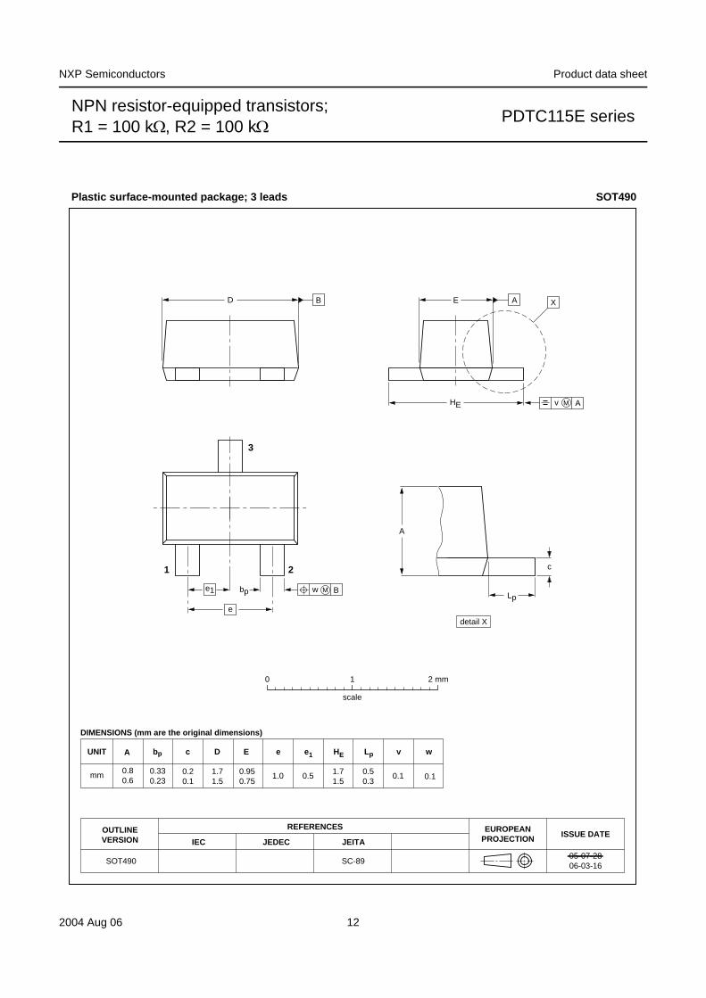
PDTC115E series
UNIT bp c D E e1 HE Lp wv
REFERENCESOUTLINEVERSION
EUROPEANPROJECTION ISSUE DATE
05-07-2806-03-16
IEC JEDEC JEITA
mm 0.330.23
0.20.1
1.71.5
0.950.75
0.5
e
1.0 1.71.5
0.10.1
DIMENSIONS (mm are the original dimensions)
0.50.3
SOT490 SC-89
bp
D
e1
e
A
Lp
detail X
HE
E
w M
v M A
B
AB
0 1 2 mm
scale
A
0.80.6
c
X
1 2
3
Plastic surface-mounted package; 3 leads SOT490
2004 Aug 06 12
NXP Semiconductors Product data sheet
NPN resistor-equipped transistors; R1 = 100 kΩ, R2 = 100 kΩ
PDTC115E series
DATA SHEET STATUS
Notes1. Please consult the most recently issued document before initiating or completing a design.2. The product status of device(s) described in this document may have changed since this document was published
and may differ in case of multiple devices. The latest product status information is available on the Internet at URL http://www.nxp.com.
DOCUMENTSTATUS(1)
PRODUCT STATUS(2) DEFINITION
Objective data sheet Development This document contains data from the objective specification for product development.
Preliminary data sheet Qualification This document contains data from the preliminary specification. Product data sheet Production This document contains the product specification.
DISCLAIMERS
General ⎯ Information in this document is believed to be accurate and reliable. However, NXP Semiconductors does not give any representations or warranties, expressed or implied, as to the accuracy or completeness of such information and shall have no liability for the consequences of use of such information.
Right to make changes ⎯ NXP Semiconductors reserves the right to make changes to information published in this document, including without limitation specifications and product descriptions, at any time and without notice. This document supersedes and replaces all information supplied prior to the publication hereof.
Suitability for use ⎯ NXP Semiconductors products are not designed, authorized or warranted to be suitable for use in medical, military, aircraft, space or life support equipment, nor in applications where failure or malfunction of an NXP Semiconductors product can reasonably be expected to result in personal injury, death or severe property or environmental damage. NXP Semiconductors accepts no liability for inclusion and/or use of NXP Semiconductors products in such equipment or applications and therefore such inclusion and/or use is at the customer’s own risk.
Applications ⎯ Applications that are described herein for any of these products are for illustrative purposes only. NXP Semiconductors makes no representation or warranty that such applications will be suitable for the specified use without further testing or modification.
Limiting values ⎯ Stress above one or more limiting values (as defined in the Absolute Maximum Ratings System of IEC 60134) may cause permanent damage to the device. Limiting values are stress ratings only and operation of the device at these or any other conditions
above those given in the Characteristics sections of this document is not implied. Exposure to limiting values for extended periods may affect device reliability.
Terms and conditions of sale ⎯ NXP Semiconductors products are sold subject to the general terms and conditions of commercial sale, as published at http://www.nxp.com/profile/terms, including those pertaining to warranty, intellectual property rights infringement and limitation of liability, unless explicitly otherwise agreed to in writing by NXP Semiconductors. In case of any inconsistency or conflict between information in this document and such terms and conditions, the latter will prevail.
No offer to sell or license ⎯ Nothing in this document may be interpreted or construed as an offer to sell products that is open for acceptance or the grant, conveyance or implication of any license under any copyrights, patents or other industrial or intellectual property rights.
Export control ⎯ This document as well as the item(s) described herein may be subject to export control regulations. Export might require a prior authorization from national authorities.
Quick reference data ⎯ The Quick reference data is an extract of the product data given in the Limiting values and Characteristics sections of this document, and as such is not complete, exhaustive or legally binding.
2004 Aug 06 13
NXP Semiconductors
Contact information
For additional information please visit: http://www.nxp.com For sales offices addresses send e-mail to: [email protected]
© NXP B.V. 2009
All rights are reserved. Reproduction in whole or in part is prohibited without the prior written consent of the copyright owner.The information presented in this document does not form part of any quotation or contract, is believed to be accurate and reliable and may be changed without notice. No liability will be accepted by the publisher for any consequence of its use. Publication thereof does not convey nor imply any license
Customer notification
This data sheet was changed to reflect the new company name NXP Semiconductors, including new legal definitions and disclaimers. No changes were made to the technical content, except for package outline drawings which were updated to the latest version.
under patent- or other industrial or intellectual property rights.Printed in The Netherlands R75/05/pp14 Date of release: 2004 Aug 06 Document order number: 9397 750 13666


![PDTC144E series NPN resistor-equipped transistors; R1 = 47 ... · NPN resistor-equipped transistors; R1 = 47 k , R2 = 47 k 5. Limiting values Table 6. Limiting values [1] Device mounted](https://img.pdfslide.us/doc/110x75/5f6af1df5184727ecd25db5a/pdtc144e-series-npn-resistor-equipped-transistors-r1-47-npn-resistor-equipped.jpg)