Embed Size (px)
Citation preview
Data Sheet
Single-cell Li-Ion Charger IC with System Power Management AUR9807
AUR9807 Document number: DS37580 Rev. 1 - 3
1 of 23 www.diodes.com
October 2014 © Diodes Incorporated
NOT RECOMMENDED FOR NEW DESIGN
General Description
The AUR9807 is a single-cell Li-ion charger IC with
system power management feature. It charges the
battery and power the system simultaneously. The
maximum charging current (up to 1.5A) is set by
external resistor for fast charging. The output
voltage for the system is regulated to a nominal
value (three different versions available: 4.4V, 5V or
6V); the actual value of the output voltage depends
on the input voltage from the adapter, the charging
current and the system loading. With the decrease of
the input voltage or the increase of the system
loading current, the output voltage drops. When the
output voltage drops to a predetermined value
(VAPM-REG), the Active Power Management function
is activated and tries to maintain the output voltage
at VAPM-REG; the AUR9807 will suffice the system
loading with first priority and reduce the charging
current temporarily, i.e. under heavy load condition,
the AUR9807 charges the battery with the remaining
available current to keep the output voltage at VAPM.
In this manner, the charge and discharge cycle of the
battery can be reduced.
It is possible that the AUR9807 fails to maintain the
output voltage at VAPM-REG; for example, when the
system loading current exceeds the capability of the
current-limiting AC adapter. In this scenario, the
output voltage drops to the battery voltage, and the
system is allowed to draw current from the battery.
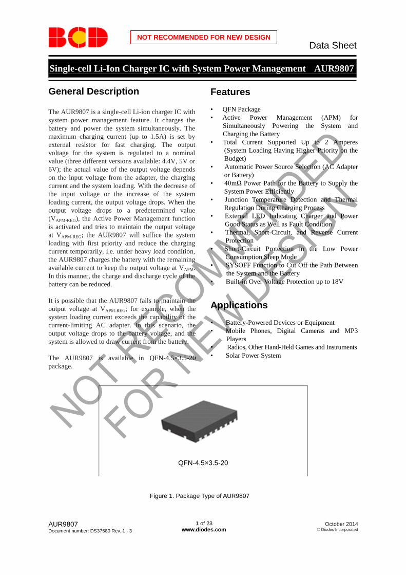
The AUR9807 is available in QFN-4.5×3.5-20
package.
Features • QFN Package
• Active Power Management (APM) for
Simultaneously Powering the System and
Charging the Battery
• Total Current Supported Up to 2 Amperes
(System Loading Having Higher Priority on the
Budget)
• Automatic Power Source Selection (AC Adapter
or Battery)
• 40mΩ Power Path for the Battery to Supply the
System Power Efficiently
• Junction Temperature Detection and Thermal
Regulation During Charging Process
• External LED Indicating Charger and Power
Good Status as Well as Fault Condition
• Thermal, Short-Circuit, and Reverse Current
Protection
• Short-Circuit Protection in the Low Power
Consumption Sleep Mode
• SYSOFF Function to Cut Off the Path Between
the System and the Battery
• Built-in Over Voltage Protection up to 18V
Applications • Battery-Powered Devices or Equipment
• Mobile Phones, Digital Cameras and MP3
Players
• Radios, Other Hand-Held Games and Instruments
• Solar Power System
Figure 1. Package Type of AUR9807
QFN-4.5×3.5-20
Data Sheet
Single-cell Li-Ion Charger IC with System Power Management AUR9807
AUR9807 Document number: DS37580 Rev. 1 - 3
2 of 23 www.diodes.com
October 2014 © Diodes Incorporated
NOT RECOMMENDED FOR NEW DESIGN
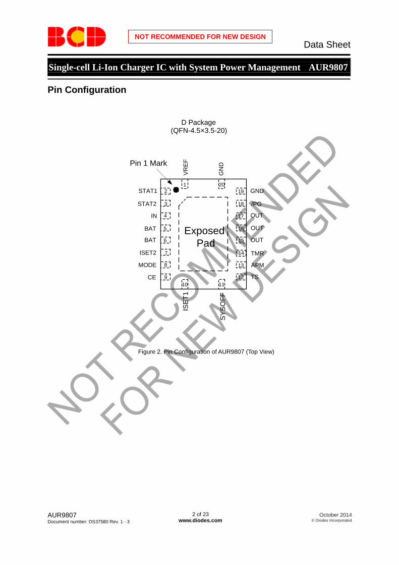
Pin Configuration
D Package (QFN-4.5×3.5-20)
Exposed
Pad
1
2
3
4
5
10
9
8
6
19
18
17
16
15
14
13
12
11
20
Pin 1 Mark
7
VR
EF
STAT1
STAT2
IN
BAT
BAT
ISET2
MODE
CE
ISE
T1
SY
SO
FF
TS
APM
TMR
OUT
/PG
GN
D
GND
OUT
OUT
Figure 2. Pin Configuration of AUR9807 (Top View)
Data Sheet
Single-cell Li-Ion Charger IC with System Power Management AUR9807
AUR9807 Document number: DS37580 Rev. 1 - 3
3 of 23 www.diodes.com
October 2014 © Diodes Incorporated
NOT RECOMMENDED FOR NEW DESIGN
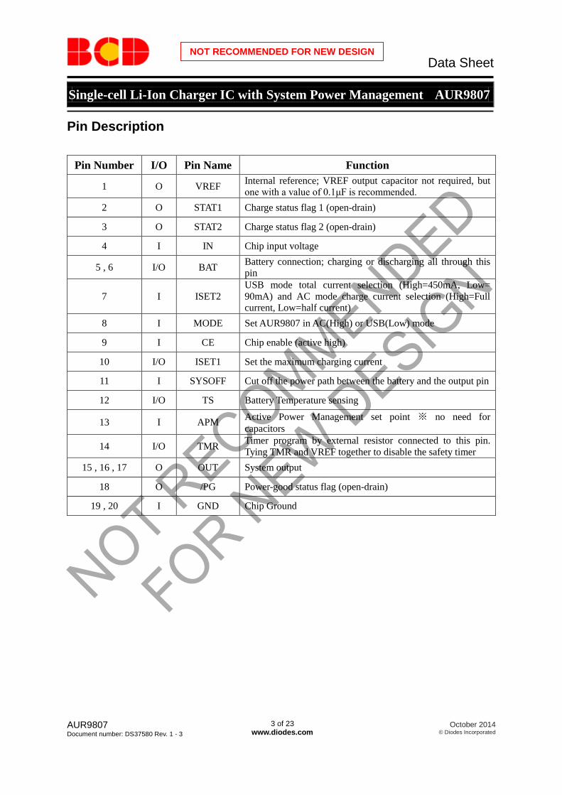
Pin Description
Pin Number I/O Pin Name Function
1 O VREF Internal reference; VREF output capacitor not required, but
one with a value of 0.1μF is recommended.
2 O STAT1 Charge status flag 1 (open-drain)
3 O STAT2 Charge status flag 2 (open-drain)
4 I IN Chip input voltage
5 , 6 I/O BAT Battery connection; charging or discharging all through this
pin
7 I ISET2
USB mode total current selection (High=450mA, Low=
90mA) and AC mode charge current selection (High=Full
current, Low=half current)
8 I MODE Set AUR9807 in AC(High) or USB(Low) mode
9 I CE Chip enable (active high)
10 I/O ISET1 Set the maximum charging current
11 I SYSOFF Cut off the power path between the battery and the output pin
12 I/O TS Battery Temperature sensing
13 I APM Active Power Management set point ※ no need for
capacitors
14 I/O TMR Timer program by external resistor connected to this pin.
Tying TMR and VREF together to disable the safety timer
15 , 16 , 17 O OUT System output
18 O /PG Power-good status flag (open-drain)
19 , 20 I GND Chip Ground
Data Sheet
Single-cell Li-Ion Charger IC with System Power Management AUR9807
AUR9807 Document number: DS37580 Rev. 1 - 3
4 of 23 www.diodes.com
October 2014 © Diodes Incorporated
NOT RECOMMENDED FOR NEW DESIGN
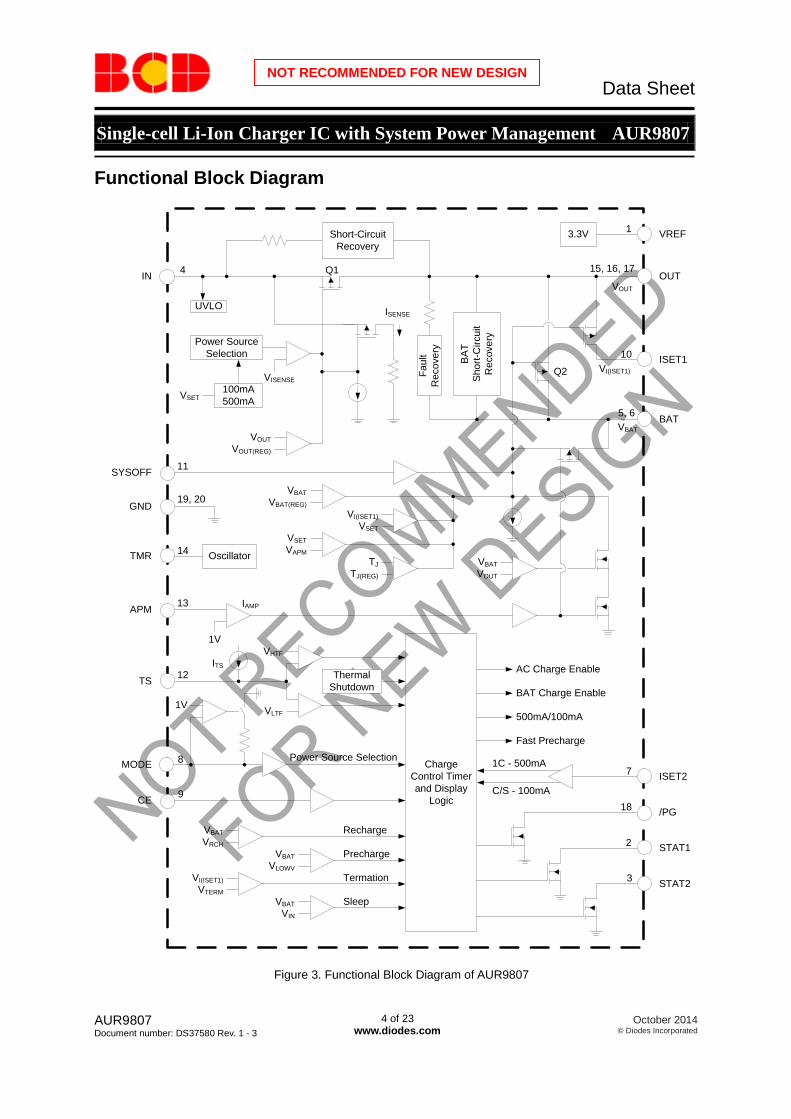
Functional Block Diagram
Charge
Control Timer
and Display
Logic
AC Charge Enable
BAT Charge Enable
500mA/100mA
Fast Precharge
VOUT
ISET2
/PG
STAT1
STAT2
1C - 500mA
C/S - 100mA
VIN
VBAT Sleep
VTERM
VI(ISET1) Termation
VLOWV
VBAT Precharge
VRCH
VBAT Recharge
CE
MODE
1V
Power Source Selection
TS
VLTF
Thermal
Shutdown
VHTF
APM
1V
INQ1
OUT
Q2
VREF3.3VShort-Circuit
Recovery
BAT
ISET1
VOUT
VSET100mA
500mA
Power Source
Selection
VISENSE
TMR Oscillator
VOUT(REG)
ISENSE
GND
UVLO
Fa
ult
Re
co
ve
ryVBAT
BA
T
Sh
ort
-Circu
it
Re
co
ve
ry
TJ(REG)
TJ
VAPM
VSET
VSET
VI(ISET1)
VBAT(REG)
VBAT
IAMP
VI(ISET1)
SYSOFF
VOUT
VBAT
ITS
1
2
3
4
5, 6
7
8
9
10
11
12
13
14
15, 16, 17
18
19, 20
Figure 3. Functional Block Diagram of AUR9807
Data Sheet
Single-cell Li-Ion Charger IC with System Power Management AUR9807
AUR9807 Document number: DS37580 Rev. 1 - 3
5 of 23 www.diodes.com
October 2014 © Diodes Incorporated
NOT RECOMMENDED FOR NEW DESIGN
G: Green
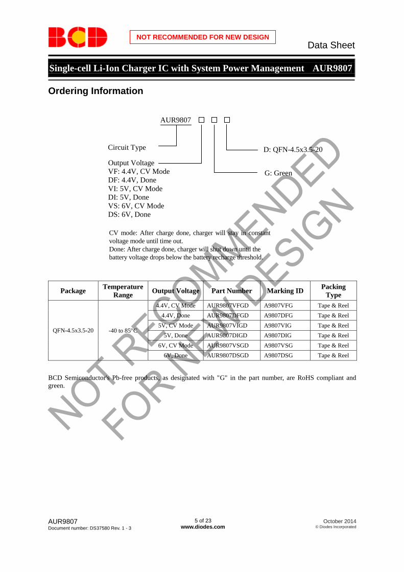
Ordering Information
AUR9807
Circuit Type
Package Temperature
Range Output Voltage Part Number Marking ID
Packing
Type
QFN-4.5x3.5-20 -40 to 85C
4.4V, CV Mode AUR9807VFGD A9807VFG Tape & Reel
4.4V, Done AUR9807DFGD A9807DFG Tape & Reel
5V, CV Mode AUR9807VIGD A9807VIG Tape & Reel
5V, Done AUR9807DIGD A9807DIG Tape & Reel
6V, CV Mode AUR9807VSGD A9807VSG Tape & Reel
6V, Done AUR9807DSGD A9807DSG Tape & Reel
BCD Semiconductor's Pb-free products, as designated with "G" in the part number, are RoHS compliant and
green.
D: QFN-4.5x3.5-20
Output Voltage
VF: 4.4V, CV Mode
DF: 4.4V, Done
VI: 5V, CV Mode
DI: 5V, Done
VS: 6V, CV Mode
DS: 6V, Done
CV mode: After charge done, charger will stay in constant
voltage mode until time out.
Done: After charge done, charger will shut down until the
battery voltage drops below the battery recharge threshold.
Data Sheet
Single-cell Li-Ion Charger IC with System Power Management AUR9807
AUR9807 Document number: DS37580 Rev. 1 - 3
6 of 23 www.diodes.com
October 2014 © Diodes Incorporated
NOT RECOMMENDED FOR NEW DESIGN
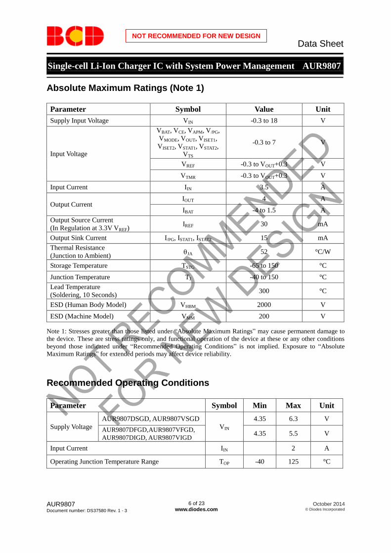
Absolute Maximum Ratings (Note 1) Parameter Symbol Value Unit
Supply Input Voltage VIN -0.3 to 18 V
Input Voltage
VBAT, VCE, VAPM, V/PG,
VMODE, VOUT, VISET1,
VISET2, VSTAT1, VSTAT2,
VTS
-0.3 to 7 V
VREF -0.3 to VOUT+0.3 V
VTMR -0.3 to VOUT+0.3 V
Input Current IIN 3.5 A
Output Current IOUT 4 A
IBAT -4 to 1.5 A
Output Source Current
(In Regulation at 3.3V VREF) IREF 30 mA
Output Sink Current I/PG, ISTAT1, ISTAT2 15 mA
Thermal Resistance
(Junction to Ambient) JA 52 °C/W
Storage Temperature TSTG -65 to 150 °C
Junction Temperature TJ -40 to 150 °C
Lead Temperature
(Soldering, 10 Seconds) 300 °C
ESD (Human Body Model) VHBM 2000 V
ESD (Machine Model) VMM 200 V Note 1: Stresses greater than those listed under “Absolute Maximum Ratings” may cause permanent damage to
the device. These are stress ratings only, and functional operation of the device at these or any other conditions
beyond those indicated under “Recommended Operating Conditions” is not implied. Exposure to “Absolute
Maximum Ratings” for extended periods may affect device reliability.
Recommended Operating Conditions
Parameter Symbol Min Max Unit
Supply Voltage
AUR9807DSGD, AUR9807VSGD
VIN
4.35 6.3 V
AUR9807DFGD,AUR9807VFGD,
AUR9807DIGD, AUR9807VIGD 4.35 5.5 V
Input Current IIN 2 A
Operating Junction Temperature Range TOP -40 125 °C
Data Sheet
Single-cell Li-Ion Charger IC with System Power Management AUR9807
AUR9807 Document number: DS37580 Rev. 1 - 3
7 of 23 www.diodes.com
October 2014 © Diodes Incorporated
NOT RECOMMENDED FOR NEW DESIGN
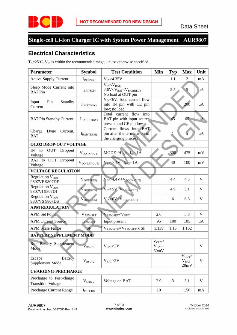
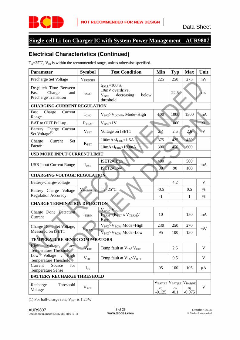
Electrical Characteristics
TA=25oC, VIN is within the recommended range, unless otherwise specified.
Parameter Symbol Test Condition Min Typ Max Unit
Active Supply Current IIN(SPLY) VIN>4.35V 1.1 2 mA
Sleep Mode Current into
BAT Pin IBAT(SLP)
VIN<VBAT,
2.6V<VBAT<VBAT(REG)
No load at OUT pin
2.5 5 μA
Input Pin Standby
Current IIN(STDBY)
VIN<6V, Total current flow
into IN pin with CE pin
low; no load
200 μA
BAT Pin Standby Current IBAT(STDBY)
Total current flow into
BAT pin with input source
present and CE pin low
45 65 μA
Charge Done Current,
BAT IBAT(TERM)
Current flows into BAT
pin after the termination of
the charging process
1 5 μA
Q1,Q2 DROP-OUT VOLTAGE
IN to OUT Dropout
Voltage VDO(IN-OUT) MODE=High , IIN=1A 300 475 mV
BAT to OUT Dropout
Voltage VDO(BAT-OUT) VBAT> 4V , IBAT=1A 40 100 mV
VOLTAGE REGULATION
Regulation VOUT
9807VF 9807DF VOUT(REG) VIN>4.4V+VDO(IN-OUT) 4.4 4.5 V
Regulation VOUT
9807VI 9807DI VOUT(REG) VIN>5V+VDO(IN-OUT) 4.9 5.1 V
Regulation VOUT
9807VS 9807DS VOUT(REG) VIN>6V+VDO(IN-OUT) 6 6.3 V
APM REGULATION
APM Set Point VAPM-SET VAPM-SET<VOUT 2.6 3.8 V
APM Current Source IAPM-SET Input present 95 100 105 μA
APM Scale Factor SF VAPM-REG=VAPM-SET x SF 1.139 1.15 1.162
BATTERY SUPPLEMENT MODE
Run Battery Supplement
Mode VBSUP1 VBAT>2V
VOUT<
VBAT–
60mV
V
Escape Battery
Supplement Mode VBSUP2 VBAT>2V
VOUT>
VBAT–
20mV
V
CHARGING-PRECHARGE
Precharge to Fast-charge
Transition Voltage VLOWV Voltage on BAT 2.9 3 3.1 V
Precharge Current Range IPRECHG 10 150 mA
Data Sheet
Single-cell Li-Ion Charger IC with System Power Management AUR9807
AUR9807 Document number: DS37580 Rev. 1 - 3
8 of 23 www.diodes.com
October 2014 © Diodes Incorporated
NOT RECOMMENDED FOR NEW DESIGN
Electrical Characteristics (Continued)
TA=25oC, VIN is within the recommended range, unless otherwise specified.
Parameter Symbol Test Condition Min Typ Max Unit
Precharge Set Voltage VPRECHG 225 250 275 mV
De-glitch Time Between
Fast Charge and
Precharge Transition
tDGLF
tFALL=100ns,
10mV overdrive,
VBAT decreasing below
threshold
22.5 ms
CHARGING-CURRENT REGULATION
Fast Charge Current
Range ICHG VBAT>VLOWV, Mode=High 100 1000 1500 mA
BAT to OUT Pull-up RPBAT VBAT<1V 1000 Ω
Battery Charge Current
Set Voltage(1)
VSET Voltage on ISET1 2.4 2.5 2.6 V
Charge Current Set
Factor KSET
100mA<ICHG<1.5A 375 425 450
10mA<ICHG<100mA 300 450 600
USB MODE INPUT CURRENT LIMIT
USB Input Current Range IUSB ISET2=High 400 500
mA ISET2=Low 80 90 100
CHARGING VOLTAGE REGULATION
Battery-charge-voltage
VBAT(REG)
4.2 V
Battery Charge Voltage
Regulation Accuracy
TA=25°C -0.5 0.5 %
-1 1 %
CHARGE TERMINATION DETECTION
Charge Done Detection
Current ITERM
VBAT>VRCH,
ITERM=(KSET x VTERM)/
RSET
10 150 mA
Charge Done Set Voltage,
Measured on ISET1 VTERM
VBAT>VRCH, Mode=High 230 250 270 mV
VBAT>VRCH, Mode=Low 95 100 130
TEMPERATURE SENSE COMPARATORS
High Voltage, Low
Temperature Threshold VLTF Temp fault at VTS>VLTF 2.5 V
Low Voltage , High
Temperature Threshold VHTF Temp fault at VTS<VHTF 0.5 V
Current Source for
Temperature Sense ITS 95 100 105 μA
BATTERY RECHARGE THRESHOLD
Recharge Threshold
Voltage VRCH
VBAT(RE
G)
-0.125
VBAT(RE
G)
-0.1
VBAT(RE
G)
-0.075
V
(1) For half-charge rate, VSET is 1.25V.
Data Sheet
Single-cell Li-Ion Charger IC with System Power Management AUR9807
AUR9807 Document number: DS37580 Rev. 1 - 3
9 of 23 www.diodes.com
October 2014 © Diodes Incorporated
NOT RECOMMENDED FOR NEW DESIGN
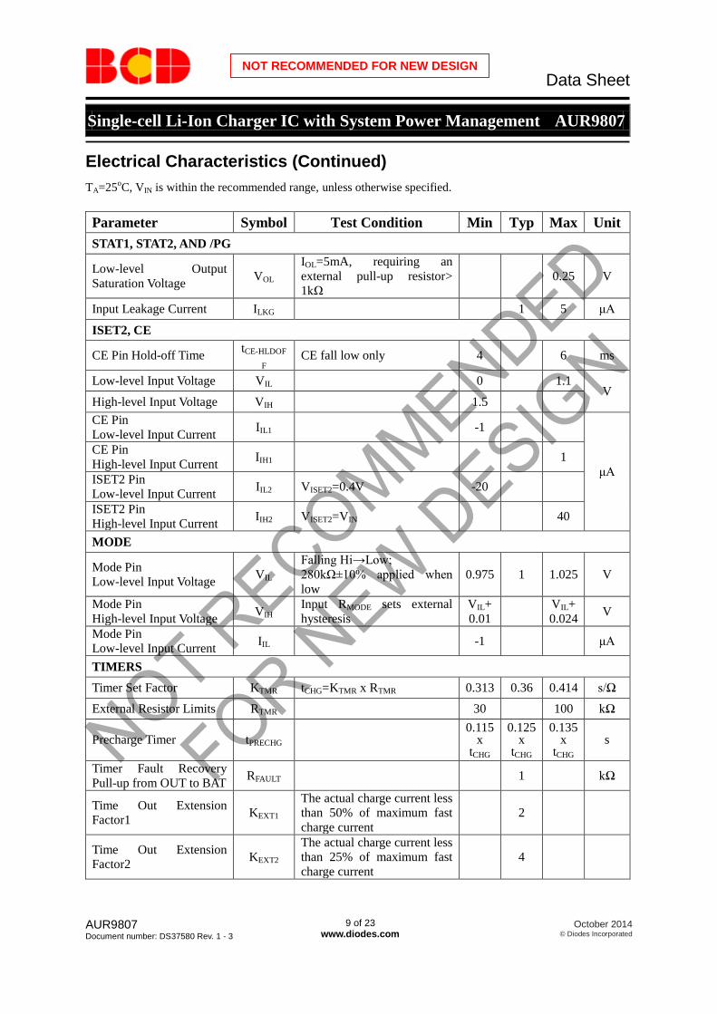
Electrical Characteristics (Continued)
TA=25oC, VIN is within the recommended range, unless otherwise specified.
Parameter Symbol Test Condition Min Typ Max Unit
STAT1, STAT2, AND /PG
Low-level Output
Saturation Voltage VOL
IOL=5mA, requiring an
external pull-up resistor>
1kΩ
0.25 V
Input Leakage Current ILKG 1 5 μA
ISET2, CE
CE Pin Hold-off Time tCE-HLDOF
F CE fall low only 4 6 ms
Low-level Input Voltage VIL 0 1.1 V
High-level Input Voltage VIH 1.5
CE Pin
Low-level Input Current IIL1 -1
μA
CE Pin
High-level Input Current IIH1 1
ISET2 Pin
Low-level Input Current IIL2 VISET2=0.4V -20
ISET2 Pin
High-level Input Current IIH2 VISET2=VIN 40
MODE
Mode Pin
Low-level Input Voltage VIL
Falling Hi→Low;
280kΩ±10% applied when
low
0.975 1 1.025 V
Mode Pin
High-level Input Voltage VIH
Input RMODE sets external
hysteresis
VIL+
0.01
VIL+
0.024 V
Mode Pin
Low-level Input Current IIL -1 μA
TIMERS
Timer Set Factor KTMR tCHG=KTMR x RTMR 0.313 0.36 0.414 s/Ω
External Resistor Limits RTMR 30 100 kΩ
Precharge Timer tPRECHG 0.115
x tCHG
0.125 x
tCHG
0.135 x
tCHG s
Timer Fault Recovery
Pull-up from OUT to BAT RFAULT 1 kΩ
Time Out Extension
Factor1 KEXT1
The actual charge current less
than 50% of maximum fast
charge current
2
Time Out Extension
Factor2 KEXT2
The actual charge current less
than 25% of maximum fast
charge current
4
Data Sheet
Single-cell Li-Ion Charger IC with System Power Management AUR9807
AUR9807 Document number: DS37580 Rev. 1 - 3
10 of 23 www.diodes.com
October 2014 © Diodes Incorporated
NOT RECOMMENDED FOR NEW DESIGN
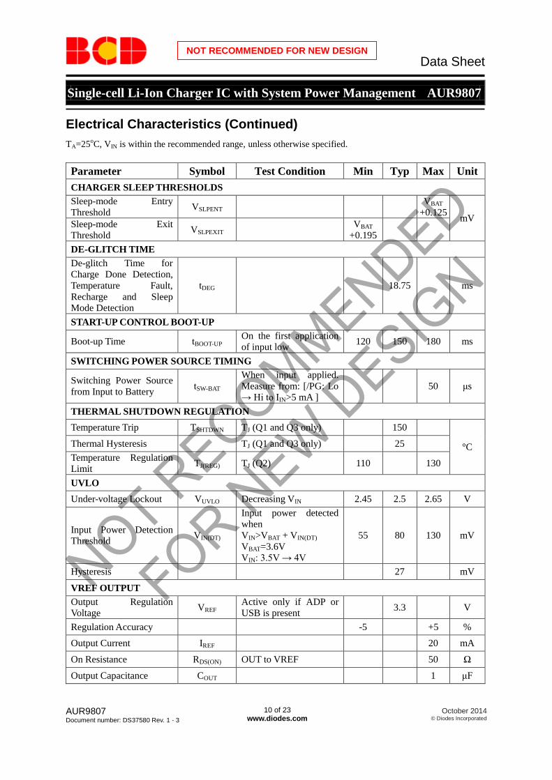
Electrical Characteristics (Continued)
TA=25oC, VIN is within the recommended range, unless otherwise specified.
Parameter Symbol Test Condition Min Typ Max Unit
CHARGER SLEEP THRESHOLDS
Sleep-mode Entry
Threshold VSLPENT
VBAT
+0.125 mV
Sleep-mode Exit
Threshold VSLPEXIT
VBAT
+0.195
DE-GLITCH TIME
De-glitch Time for
Charge Done Detection,
Temperature Fault,
Recharge and Sleep
Mode Detection
tDEG 18.75 ms
START-UP CONTROL BOOT-UP
Boot-up Time tBOOT-UP On the first application
of input low 120 150 180 ms
SWITCHING POWER SOURCE TIMING
Switching Power Source
from Input to Battery tSW-BAT
When input applied.
Measure from: [/PG: Lo
→ Hi to IIN>5 mA ]
50 μs
THERMAL SHUTDOWN REGULATION
Temperature Trip TSHTDWN TJ (Q1 and Q3 only) 150
°C Thermal Hysteresis TJ (Q1 and Q3 only) 25
Temperature Regulation
Limit TJ(REG) TJ (Q2) 110 130
UVLO
Under-voltage Lockout VUVLO Decreasing VIN 2.45 2.5 2.65 V
Input Power Detection
Threshold VIN(DT)
Input power detected
when
VIN>VBAT + VIN(DT)
VBAT=3.6V
VIN: 3.5V → 4V
55 80 130 mV
Hysteresis 27 mV
VREF OUTPUT
Output Regulation
Voltage VREF
Active only if ADP or
USB is present 3.3 V
Regulation Accuracy -5 +5 %
Output Current IREF 20 mA
On Resistance RDS(ON) OUT to VREF 50 Ω
Output Capacitance COUT 1 μF
Data Sheet
Single-cell Li-Ion Charger IC with System Power Management AUR9807
AUR9807 Document number: DS37580 Rev. 1 - 3
11 of 23 www.diodes.com
October 2014 © Diodes Incorporated
NOT RECOMMENDED FOR NEW DESIGN
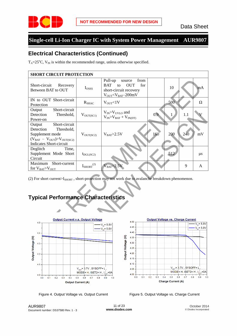
Electrical Characteristics (Continued)
TA=25oC, VIN is within the recommended range, unless otherwise specified.
SHORT CIRCUIT PROTECTION
Short-circuit Recovery
Between BAT to OUT IOSH1
Pull-up source from
BAT to OUT for
short-circuit recovery
VOUT<VBAT–200mV
10 mA
IN to OUT Short-circuit
Protection RSHAC VOUT<1V 500 Ω
Output Short-circuit
Detection Threshold,
Power-on
VOUT(SC1) VIN>VUVLO and
VIN>VBAT + VIN(DT) 0.9 1 1.1 V
Output Short-circuit
Detection Threshold,
Supplement mode
(VBAT – VOUT)>VOUT(SC2)
Indicates Short-circuit
VOUT(SC2) VBAT>2.5V 160 200 240 mV
Deglitch Time,
Supplement Mode Short
Circuit
tDGL(SC2) 512 μs
Maximum Short-current
for VBAT>VOUT ISHORT
(2) VBAT>2.5V 9 A
(2) For short current>ISHORT , short-protection may not work due to avalanche breakdown phenomenon.
Typical Performance Characteristics
Figure 4. Output Voltage vs. Output Current Figure 5. Output Voltage vs. Charge Current
Data Sheet
Single-cell Li-Ion Charger IC with System Power Management AUR9807
AUR9807 Document number: DS37580 Rev. 1 - 3
12 of 23 www.diodes.com
October 2014 © Diodes Incorporated
NOT RECOMMENDED FOR NEW DESIGN
Typical Performance Characteristics (Continued)
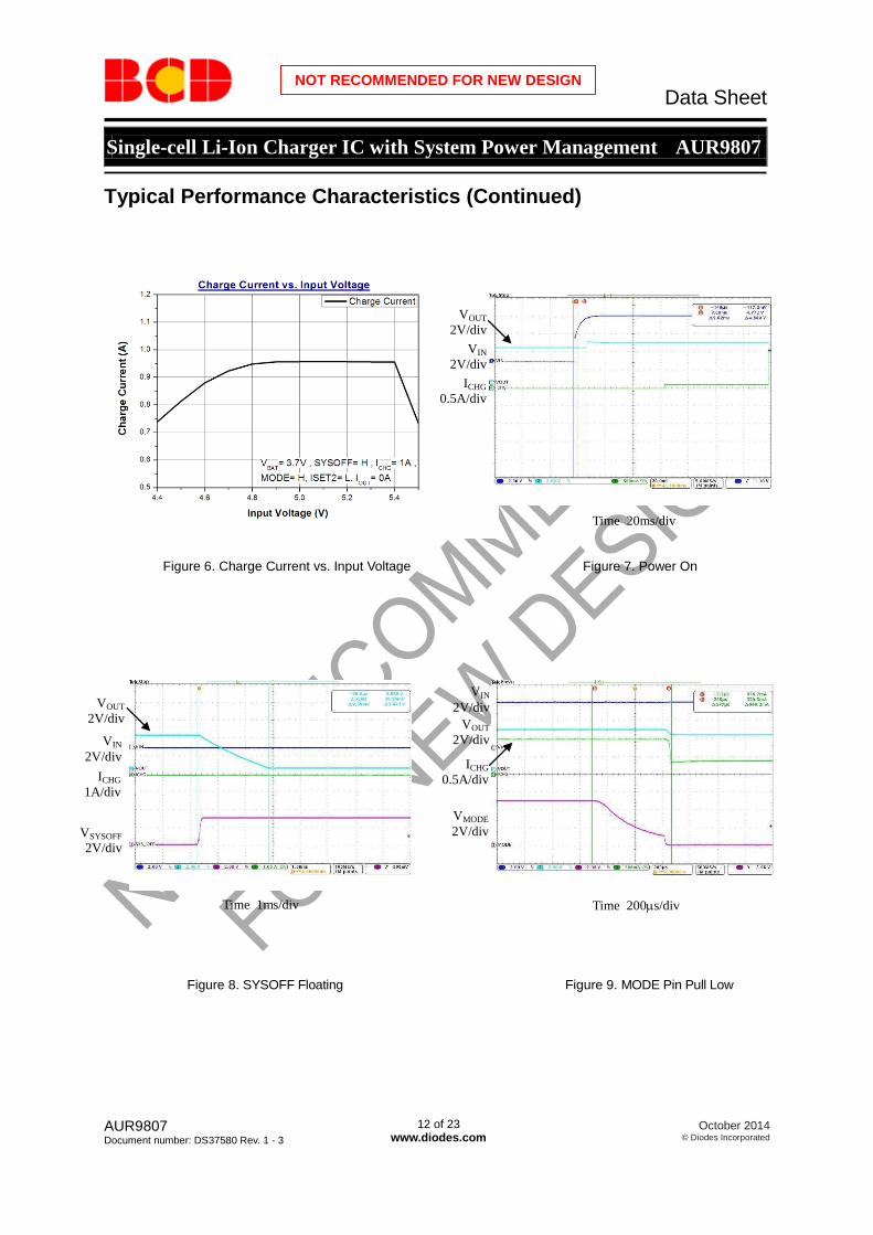
Figure 6. Charge Current vs. Input Voltage Figure 7. Power On
Figure 8. SYSOFF Floating Figure 9. MODE Pin Pull Low
VIN
2V/div
VIN
2V/div
VOUT
2V/div
ICHG
0.5A/div
VOUT
2V/div
ICHG
1A/div
VSYSOFF
2V/div
Time 20ms/div
Time 1ms/div
VOUT
2V/div
VIN
2V/div
ICHG
0.5A/div
VMODE
2V/div
Time 200s/div
Data Sheet
Single-cell Li-Ion Charger IC with System Power Management AUR9807
AUR9807 Document number: DS37580 Rev. 1 - 3
13 of 23 www.diodes.com
October 2014 © Diodes Incorporated
NOT RECOMMENDED FOR NEW DESIGN
Typical Performance Characteristics (Continued)
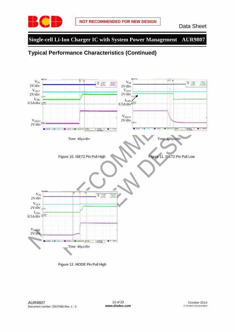
Figure 10. ISET2 Pin Pull High Figure 11. ISET2 Pin Pull Low
Figure 12. MODE Pin Pull High
VOUT
2V/div
VIN
2V/div
ICHG
0.5A/div
VISET2
2V/div
VOUT
2V/div
VIN
2V/div
ICHG
0.5A/div
VISET2
2V/div
VOUT
2V/div
VIN
2V/div
ICHG
0.5A/div
VMODE
2V/div
Time 40s/div
Time 40s/div Time 400s/div
Data Sheet
Single-cell Li-Ion Charger IC with System Power Management AUR9807
AUR9807 Document number: DS37580 Rev. 1 - 3
14 of 23 www.diodes.com
October 2014 © Diodes Incorporated
NOT RECOMMENDED FOR NEW DESIGN
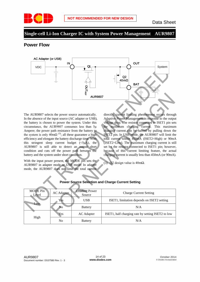
Power Flow
AUR9807
Q1
Q2
IN OUT
BAT
VDC
AC Adapter (or USB)
OU
TR
EF
+- 40 mΩ
AUR9807
Q1
Q2
IN OUT
BAT
SystemVDC
AC Adapter (or USB)
OU
TR
EF
+- 40 mΩ
The AUR9807 selects the power source automatically.
In the absence of the input source (AC adapter or USB),
the battery is chosen to power the system. Under this
circumstance, the AUR9807 consumes less than 5μ
Ampere; the power path resistance from the battery to
the system is only 40mΩ (3)
; all these guarantee a high
efficiency and elongate the battery discharge time. With
this stringent sleep current budget (<5μA), the
AUR9807 is still able to detect an output short
condition and cuts off the power path between the
battery and the system under short condition.
With the input power present, the MODE pin sets the
AUR9807 in adapter mode or USB mode. In adapter
mode, the AUR9807 does not limit the total current
directly, current limiting phenomenon occurs through
Adaptive Power Management in response to the output
voltage drop. The resistor connected to ISET1 pin sets
the maximum charging current. This maximum
charging current can be halved by pulling down the
ISET2 pin. In USB mode, the AUR9807 will limit the
total current within 450mA (ISET2=High) or 90mA
(ISET2=Low). The maximum charging current is still
set by the resistor connected to ISET1 pin; however,
because of this current limiting feature, the actual
charging current is usually less than 450mA (or 90mA).
(3) Q2 design value is 40mΩ.
Power Source Selection and Charge Current Setting
MODE Pin
Level AC Adapter
Loading Power
Source Charge Current Setting
Low Yes USB ISET1, limitation depends on ISET2 setting
No Battery N/A
High Yes AC Adapter ISET1, half charging rate by setting ISET2 to low
No Battery N/A
Data Sheet
Single-cell Li-Ion Charger IC with System Power Management AUR9807
AUR9807 Document number: DS37580 Rev. 1 - 3
15 of 23 www.diodes.com
October 2014 © Diodes Incorporated
NOT RECOMMENDED FOR NEW DESIGN
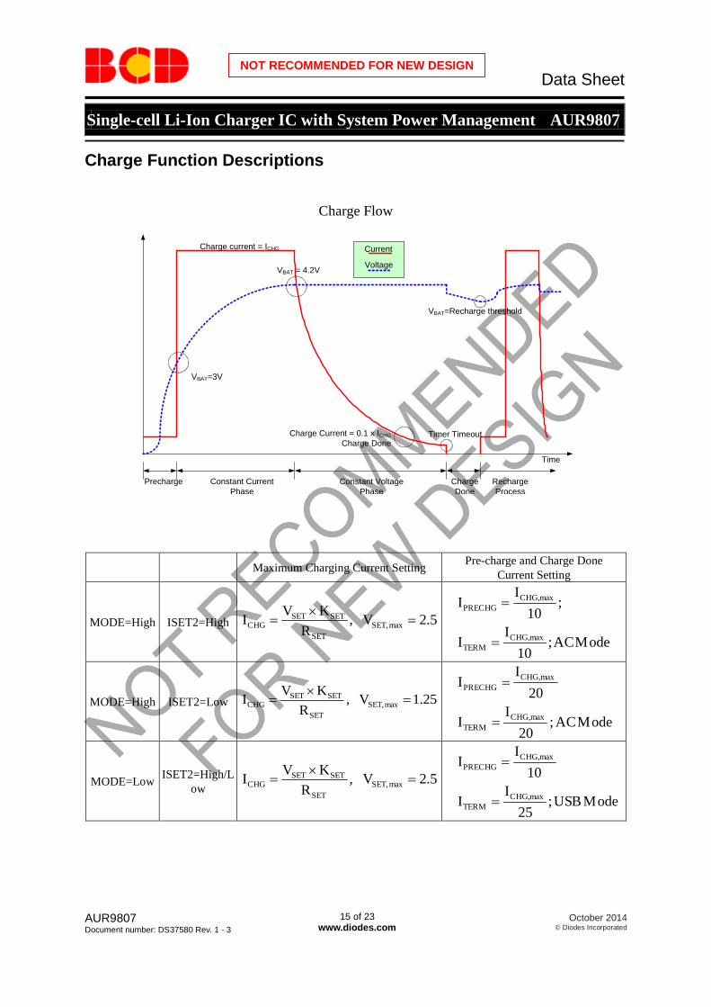
Charge Function Descriptions
Charge Flow
Time
VBAT=3V
VBAT = 4.2V
Constant Current
Phase
Constant Voltage
Phase
Charge Current = 0.1 x ICHG
Charge DoneTimer Timeout
VBAT=Recharge threshold
Charge
Done
Current
Voltage
Charge current = ICHG
Precharge Recharge
Process
Maximum Charging Current Setting Pre-charge and Charge Done
Current Setting
MODE=High ISET2=High 2.5V,R
KVI maxSET,
SET
SETSETCHG
ModeAC;10
II
;10
II
maxCHG,
TERM
maxCHG,
PRECHG
MODE=High ISET2=Low 1.25V,R
KVI maxSET,
SET
SETSETCHG
ModeAC;20
II
20
II
maxCHG,
TERM
maxCHG,
PRECHG
MODE=Low ISET2=High/L
ow 2.5V,
R
KVI maxSET,
SET
SETSETCHG
ModeUSB;25
II
10
II
maxCHG,
TERM
maxCHG,
PRECHG
Data Sheet
Single-cell Li-Ion Charger IC with System Power Management AUR9807
AUR9807 Document number: DS37580 Rev. 1 - 3
16 of 23 www.diodes.com
October 2014 © Diodes Incorporated
NOT RECOMMENDED FOR NEW DESIGN
Charge Function Descriptions (Continued)
The maximum charging current, the pre-charge
current and charge done current setting are given in
the above table. The charging process begins with a
pre-charge phase; when the battery voltage reaches
the pre-charge threshold VLOWV, the charger enters
the constant current mode. At this stage, the charger
tries to charge the battery with the maximum
charging current (a constant); however, the actual
charging current may be lower due to Active Power
Management activated by large system loading or
insufficient input current capability. The thermal
fold-back mechanism also reduces the actual
charging current when the junction temperature is
over 110°C. The battery voltage rises gradually with
the constant current entering the battery.
When the battery voltage reaches VBAT(REG), the
charger enters the constant voltage mode. At this
stage, the charger keeps the battery voltage at
VBAT(REG) with a decreasing charging current. When
the charging current drops below the charge done
current setting, nominally the charging process is
complete (this can be observed from the external
indicator). Depending on different versions, after the
charge done status indicated, the charger will stop
providing charging current completely or stay in
constant voltage mode till time out. When the battery
voltage drops below the recharge threshold, a new
charge cycle begins.
Example:
With a RSET=1kΩ, the maximum charging current is
about 1A for ISET2=High and 0.5A for ISET2=Low.
The pre-charge current IPRECHG is 100mA. The charge
done current setting is 100mA for AC mode and
40mA for USB mode. Note the absolute values of
pre-charge current and charge done current setting do
not vary with ISET2.
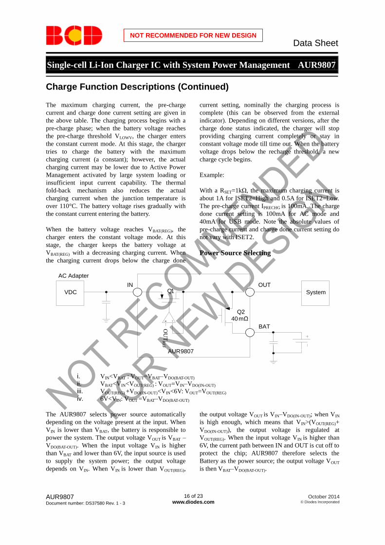
Power Source Selecting
AUR9807
Q1
Q2
IN OUT
BAT
SystemVDC
AC Adapter
OU
TR
EF
+- 40 mΩ
i. VIN<VBAT : VOUT=VBAT–VDO(BAT-OUT)
ii. VBAT<VIN<VOUT(REG) : VOUT=VIN–VDO(IN-OUT)
iii. VOUT(REG) +VDO(IN-OUT)<VIN<6V: VOUT=VOUT(REG)
iv. 6V<VIN: VOUT =VBAT–VDO(BAT-OUT)
The AUR9807 selects power source automatically
depending on the voltage present at the input. When
VIN is lower than VBAT, the battery is responsible to
power the system. The output voltage VOUT is VBAT –
VDO(BAT-OUT). When the input voltage VIN is higher
than VBAT and lower than 6V, the input source is used
to supply the system power; the output voltage
depends on VIN. When VIN is lower than VOUT(REG),
the output voltage VOUT is VIN–VDO(IN-OUT); when VIN
is high enough, which means that VIN>(VOUT(REG)+
VDO(IN-OUT)), the output voltage is regulated at
VOUT(REG). When the input voltage VIN is higher than
6V, the current path between IN and OUT is cut off to
protect the chip; AUR9807 therefore selects the
Battery as the power source; the output voltage VOUT
is then VBAT–VDO(BAT-OUT).
Data Sheet
Single-cell Li-Ion Charger IC with System Power Management AUR9807
AUR9807 Document number: DS37580 Rev. 1 - 3
17 of 23 www.diodes.com
October 2014 © Diodes Incorporated
NOT RECOMMENDED FOR NEW DESIGN
NTC
Li Battery1µF
BAT
TS
VLTF
VHTF
100µA
AUR9807
LO
GIC
UN
IT
Charge Function Descriptions (Continued)
Active Power Management (APM)
AC MODE (MODE=HIGH)
i. VAPM-REG<VOUT : Normal Mode; ICHG determined
by RSET
ii. VBAT<VOUT<VAPM-REG : APM mode ; ICHG= Isupply
max–IOUT
iii. VOUT<VBAT : BAT supply mode
USB 500 MODE (MODE=LOW ,
ISET2=HIGH)
i. VAPM-REG<VOUT: Normal Mode; ICHG determined
by RSET
ii. VBAT<VOUT<VAPM-REG : APM mode; ICHG =
450mA – IOUT
iii. VOUT<VBAT: BAT supply mode
USB 100 MODE (MODE=LOW ,
ISET2=LOW)
i. VAPM-REG<VOUT : Normal Mode; ICHG determined
by RSET
ii. VBAT<VOUT<VAPM-REG : APM mode; ICHG=
90mA–IOUT
iii. VOUT<VBAT : BAT supply mode
The active power management feature adjusts the
charging current to resist the output voltage drop due to
heavy system loading or insufficient input driving
capability. In the extreme situation, the charging current
flow would be reversed (the battery helps to supply the
system power). The active power management
regulation voltage VAPM-REG is given by:
VAPM-REG = IAPM-SET×RAPM × SF(4)
When the output voltage is higher than VAPM-REG, the
input source is capable of providing the charging
current (set by RSET) and output current (determined by
system loading) simultaneously. When the output
voltage goes down and reaches VAPM-REG due to an
increasing loading, AUR9807 starts to reduce the
charging current and tries to keep the output voltage at
VAPM-REG. Because AUR9807 uses the remaining
available current to charge the battery, the charging
current can be estimated as Isupply max – IOUT. In AC mode,
the Isupply max is determined by the driving capability of
the AC adapter and AUR9807 itself (usually the
limiting factor is the AUR9807, and Isupply max is about
2A). The Isupply max is determined by the ISET2 setting in
USB mode (Isupply max is about 450mA with ISET2 high,
and Isupply max is about 90mA with ISET2 low).
When the loading current keeps increasing and exceeds
Isupply max, the AUR9807 can not prevent the output
voltage dropping below VAPM-REG even the charging
current is reduced to zero. When the output voltage
drops below the battery voltage, the battery helps to
supply the loading current and keeps the output voltage
roughly at VBAT. At this situation, we have:
IOUT = Isupply max+IBAT(5)
(4) RAPM<38kΩ: VAPM-REG=IAPM-SET×RAPM×SF
RAPM>41kΩ: The VAPM-REG is set to a
predetermined fixed value (4.26V)
(5) IBAT=(VBAT–VOUT) / (40mΩ Power Path
Resistance)
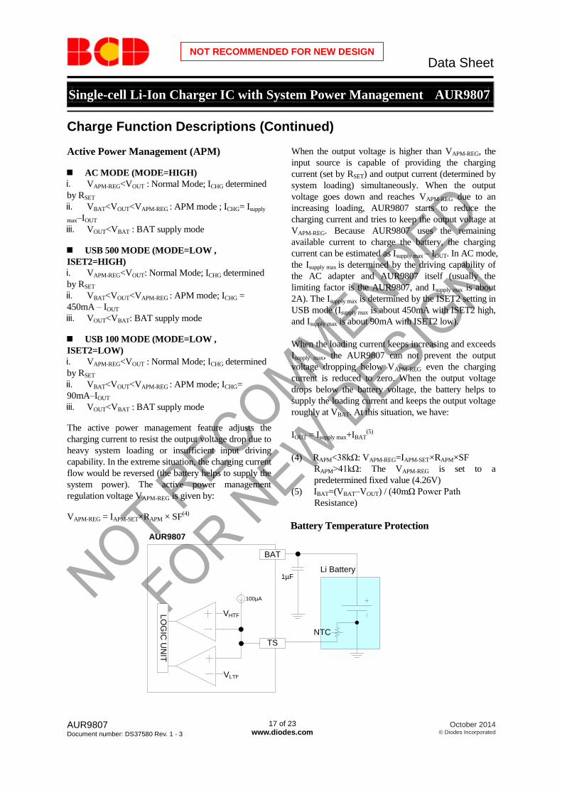
Battery Temperature Protection
Data Sheet
Single-cell Li-Ion Charger IC with System Power Management AUR9807
AUR9807 Document number: DS37580 Rev. 1 - 3
18 of 23 www.diodes.com
October 2014 © Diodes Incorporated
NOT RECOMMENDED FOR NEW DESIGN
Charge Function Descriptions (Continued) The AUR9807 interrupts the charging process when the
battery temperature is out of normal range. It provides a
100μA sensing current to the negative-temperature
coefficient resistor (on the battery side) through the TS
pin. The battery protection is achieved by constantly
monitoring the voltage at the TS pin. When this voltage
is higher than VLTF (nominally 2.5V) or lower than
VHTF (nominally 0.5V), an under-temperature or
over-temperature condition is detected. For an usual
103AT-type NTC resistor, the corresponding
temperature range is between 0°C and 45°C. The
normal battery temperature range can be modified by
adjusting the NTC resistor or by adding extra resistor
network between the TS pin and the
negative-temperature coefficient resistor. The charging
process would resume after the battery temperature
goes back within the normal range.
Charge Timeout Setting The charge timeout setting is programmed by the
resistor RTMR connected between the TMR and ground
pin. The timeout setting is given by:
tCHG = KTMR × RTMR
A suggested 36kΩ RTMR gives a 3.6 hrs timeout setting
because the nominal value of KTMR is 0.36 sec/Ω. In the
actual charging process, the charging duration is
elongated if the charging current can not reach the
maximum current setting (again this relates to system
loading and environment temperature); therefore, it is
possible that the charging process is still on progress
while the 3.6 hrs timeout limit has been reached. To
circumvent this problem, the actual charging current is
monitored and the clock rate of the timer counter is
halved if the charging current is less than 50% of the
maximum fast charging current. This is equivalent to
modify the timeout setting temporarily by the following
equation:
tCHG = KEXT1 x KTMR × RTMR, where KEXT1=2
If the actual charging current is less than one fourth the
maximum fast charging current, the time out counter
rate is reduced to 25%. The temporary timeout setting
is given by:
tCHG = KEXT2 x KTMR × RTMR, where KEXT2=4
Once the abnormal condition is removed (high
temperature or heavy loading), the charging current
resumes the maximum values (set by RSET), and the
time out counter will operate in normal rate.
Charge Status Indicator
Status STAT1 STAT2
Pre-charge ON ON
Constant current and constant
voltage charge ON OFF
Charge done OFF ON
Fault condition (time out,
sleep mode, or OTP) OFF OFF
The open drain pins STAT1 and STAT2 provides the
information about the charger status when the CE pin
(chip enable) is set to high. The various charger status
and the corresponding STAT1 and STAT2 levels are
given in the above Table. Connect these pins to the host
processor or LEDS to indicate the charger status.
Short Circuit Protection AUR9807 provides short circuit protection for both the
input and the battery. When VIN is larger than VBAT, AC
adapter (or USB port) is chosen as the power source. If
the output voltage is lower than 1V (VOUT(SC1)) for more
than tDGL(SC), a short circuit condition is detected; the
power path between the input and the output will be cut
off. The charging process will be interrupted. A 500Ω
resistor is used to pull up the output voltage; if the load
at the output is removed, the output voltage can be
pulled up and the short circuit condition is dissolved.
Similarly, when the battery is chosen as the power
source, an output voltage lower than the battery voltage
by 200mV (VOUT(SC2)) longer than tDGL(SC) will trigger
the short circuit protection mechanism (this
corresponds to a 5A loading current). A 10mA current
source is used to pull up the output and detect the
removal of the short condition. The power consumption
is less than 5μA under the battery supply mode;
however, AUR9807 is still able to monitor the output
voltage and detect a short circuit condition with this
limiting current budget.
SYSOFF Function The SYSOFF function is used to cut off the power path
between the battery and the output. This means the
Data Sheet
Single-cell Li-Ion Charger IC with System Power Management AUR9807
AUR9807 Document number: DS37580 Rev. 1 - 3
19 of 23 www.diodes.com
October 2014 © Diodes Incorporated
NOT RECOMMENDED FOR NEW DESIGN
Charge Function Descriptions (Continued)
charger function can be disabled by pulling up the
SYSOFF pin; in this mode, the AUR9807 is almost a
regulator to power the system. Because the power path
is cut off, the output voltage will drop to zero when the
input source is removed, the battery will not be used to
power the system. The SYSOFF pin is pulled high
internally; therefore, this pin should be pulled to ground
for normal operation.
Recharge Process and Timer Fault
Elimination If timeout occurs and the battery voltage is higher
than the recharge threshold, the charger will stay in
the charge done mode until the battery voltage drops
below the recharge threshold. Once the battery
voltage drops below the recharge threshold, a new
charge cycle starts.
If timeout occurs and the battery voltage is lower
than the recharge threshold, the charger will indicate
a fault condition and an internal resistor between
output and battery will try to pull up the battery
voltage. If the internal resistor is unable to pull up the
battery voltage to the recharge threshold, the charger
will stay in fault condition. Once the battery voltage
is higher than the recharge threshold, the charger
removes the pull-up resistor, leaves the fault
condition and stay in the charge done mode
temporarily. The charger then waits the battery
voltage to drop below the recharge threshold and
starts a new charge cycle.
Data Sheet
Single-cell Li-Ion Charger IC with System Power Management AUR9807
AUR9807 Document number: DS37580 Rev. 1 - 3
20 of 23 www.diodes.com
October 2014 © Diodes Incorporated
NOT RECOMMENDED FOR NEW DESIGN
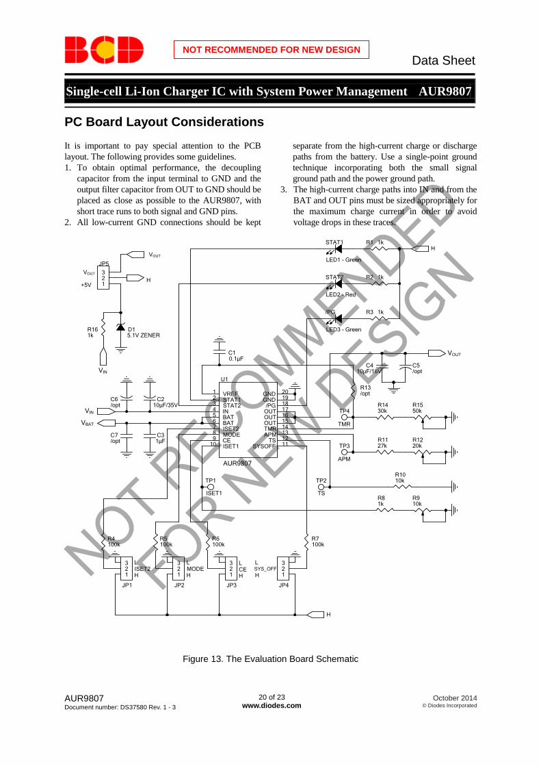
PC Board Layout Considerations
It is important to pay special attention to the PCB
layout. The following provides some guidelines.
1. To obtain optimal performance, the decoupling
capacitor from the input terminal to GND and the
output filter capacitor from OUT to GND should be
placed as close as possible to the AUR9807, with
short trace runs to both signal and GND pins.
2. All low-current GND connections should be kept
separate from the high-current charge or discharge
paths from the battery. Use a single-point ground
technique incorporating both the small signal
ground path and the power ground path.
3. The high-current charge paths into IN and from the
BAT and OUT pins must be sized appropriately for
the maximum charge current in order to avoid
voltage drops in these traces.
VBAT
R6100k
R1010k
JP1
123
R13/opt
U1
AUR9807
123456
11129
10
87
181716151413
1920VREF
STAT1STAT2INBATBAT
SYSOFFTSCE
ISET1
MODEISET2
/PGOUTOUTOUTTMRAPM
GNDGND
LED1 - Green
STAT1
JP5
123
VIN
C210μF/35V
C10.1μF
R161k
TP4
TMR
VOUT
C31μF
LCEH
R1430k
C7/opt
R4100k
LMODEH
H
JP4
123L
ISET2H
JP2
123
D15.1V ZENER
R910k
TP1
ISET1
R1550k
VOUT
+5V
R5100k
C6/opt
VOUT
VIN
JP3
123
R81k
R3 1k
R7100k
R2 1k
R1127k
C410μF/16V
LED3 - Green
/PG
C5/opt
H
LSYS_OFF
H
TP3
APM
R1 1k
TP2
TS
H
R1220k
LED2 - Red
STAT2
Figure 13. The Evaluation Board Schematic
Data Sheet
Single-cell Li-Ion Charger IC with System Power Management AUR9807
AUR9807 Document number: DS37580 Rev. 1 - 3
21 of 23 www.diodes.com
October 2014 © Diodes Incorporated
NOT RECOMMENDED FOR NEW DESIGN
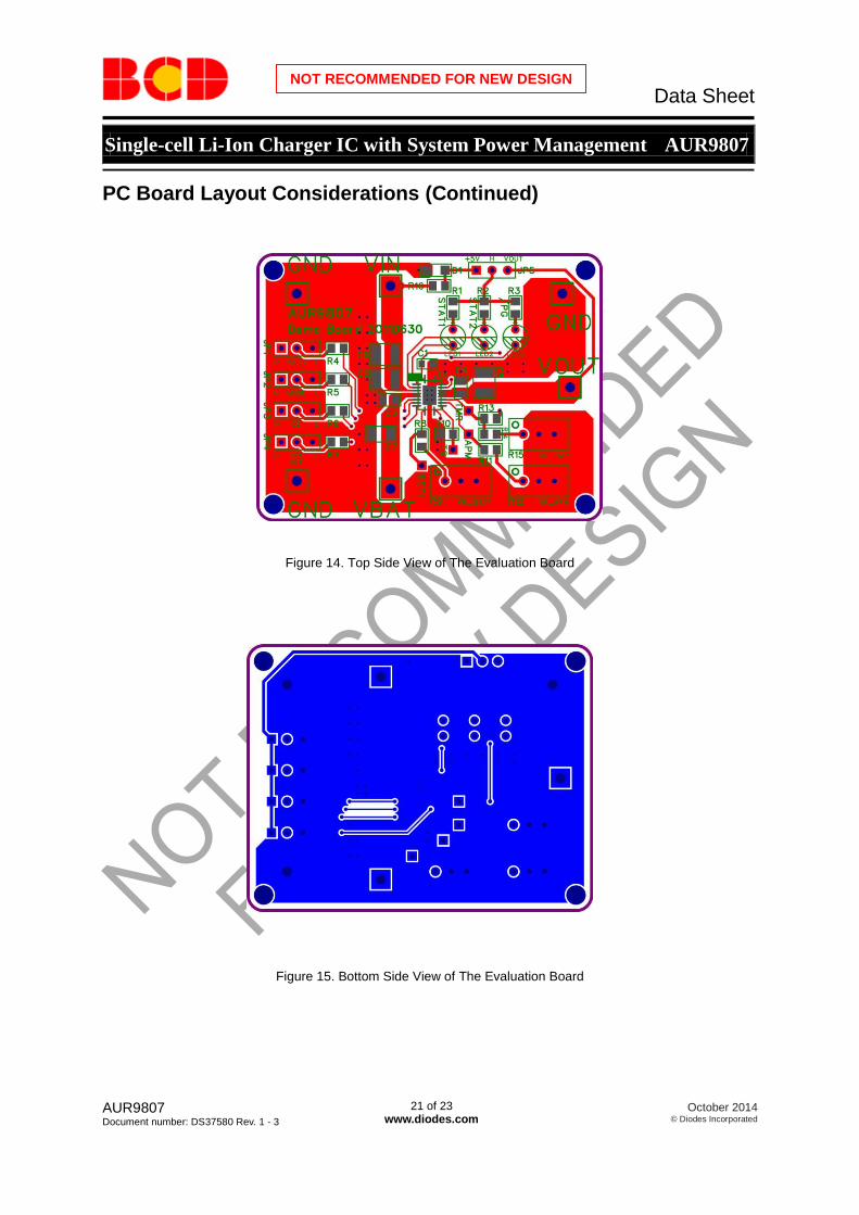
PC Board Layout Considerations (Continued)
Figure 14. Top Side View of The Evaluation Board
Figure 15. Bottom Side View of The Evaluation Board
Data Sheet
Single-cell Li-Ion Charger IC with System Power Management AUR9807
AUR9807 Document number: DS37580 Rev. 1 - 3
22 of 23 www.diodes.com
October 2014 © Diodes Incorporated
NOT RECOMMENDED FOR NEW DESIGN
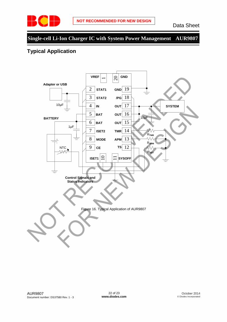
Typical Application
2
4
5
6
8
9
7
10
11
13
12
14
16
17
18
19
15
3
RTMR
RAPM
RSET
10μFSYSTEMIN
VREF
ISET2
STAT1
/PG
CE
MODE
GND
SYSOFF
TMR
APM
ISET1
TS
BAT
OUT
Control Signals and
Status Indicators
STAT2
BAT
GND
Adapter or USB
BATTERY
1 20
OUT
OUT
NTC
1μF
10μF
Figure 16. Typical Application of AUR9807
Data Sheet
Single-cell Li-Ion Charger IC with System Power Management AUR9807
AUR9807 Document number: DS37580 Rev. 1 - 3
23 of 23 www.diodes.com
October 2014 © Diodes Incorporated
NOT RECOMMENDED FOR NEW DESIGN
Mechanical Dimensions
QFN-4.5×3.5-20 Unit: mm(inch)
N20 N1
N2
N9
N11 N10
N19
N12
BSC
4.500(0.177)
3.500(0.138)
BSC
0.700(0.027)
0.800(0.031)
Pin 1 Mark
1.950(0.077)
2.100(0.083)
0.300(0.012)
0.500(0.020)
2.950(0.116)
0.180(0.007)
0.300(0.012)
0.500(0.020)
BSC
0.000(0.000)
0.050(0.002)
0.200(0.008)
REF
1.500(0.059)
BSC
3.100(0.122)
IMPORTANT NOTICE
BCD Semiconductor Manufacturing Limited reserves the right to make changes without further notice to any products or specifi-cations herein. BCD Semiconductor Manufacturing Limited does not assume any responsibility for use of any its products for anyparticular purpose, nor does BCD Semiconductor Manufacturing Limited assume any liability arising out of the application or useof any its products or circuits. BCD Semiconductor Manufacturing Limited does not convey any license under its patent rights orother rights nor the rights of others.
- Wafer FabShanghai SIM-BCD Semiconductor Manufacturing Limited800, Yi Shan Road, Shanghai 200233, ChinaTel: +86-21-6485 1491, Fax: +86-21-5450 0008
BCD Semiconductor Manufacturing LimitedMAIN SITE
REGIONAL SALES OFFICEShenzhen OfficeShanghai SIM-BCD Semiconductor Manufacturing Co., Ltd. Shenzhen OfficeAdvanced Analog Circuits (Shanghai) Corporation Shenzhen OfficeRoom E, 5F, Noble Center, No.1006, 3rd Fuzhong Road, Futian District, Shenzhen 518026, China Tel: +86-755-8826 7951Fax: +86-755-8826 7865
Taiwan OfficeBCD Semiconductor (Taiwan) Company Limited4F, 298-1, Rui Guang Road, Nei-Hu District, Taipei, TaiwanTel: +886-2-2656 2808Fax: +886-2-2656 2806
USA OfficeBCD Semiconductor Corporation30920 Huntwood Ave. Hayward,CA 94544, U.S.ATel : +1-510-324-2988Fax: +1-510-324-2788
- IC Design GroupAdvanced Analog Circuits (Shanghai) Corporation8F, Zone B, 900, Yi Shan Road, Shanghai 200233, ChinaTel: +86-21-6495 9539, Fax: +86-21-6485 9673
BCD Semiconductor Manufacturing Limited
http://www.bcdsemi.com
BCD Semiconductor Manufacturing Limited
IMPORTANT NOTICE
BCD Semiconductor Manufacturing Limited reserves the right to make changes without further notice to any products or specifi-cations herein. BCD Semiconductor Manufacturing Limited does not assume any responsibility for use of any its products for anyparticular purpose, nor does BCD Semiconductor Manufacturing Limited assume any liability arising out of the application or useof any its products or circuits. BCD Semiconductor Manufacturing Limited does not convey any license under its patent rights orother rights nor the rights of others.
- Wafer FabShanghai SIM-BCD Semiconductor Manufacturing Co., Ltd.800 Yi Shan Road, Shanghai 200233, ChinaTel: +86-21-6485 1491, Fax: +86-21-5450 0008
MAIN SITE
REGIONAL SALES OFFICEShenzhen OfficeShanghai SIM-BCD Semiconductor Manufacturing Co., Ltd., Shenzhen OfficeUnit A Room 1203, Skyworth Bldg., Gaoxin Ave.1.S., Nanshan District, Shenzhen,China Tel: +86-755-8826 7951Fax: +86-755-8826 7865
Taiwan OfficeBCD Semiconductor (Taiwan) Company Limited4F, 298-1, Rui Guang Road, Nei-Hu District, Taipei, TaiwanTel: +886-2-2656 2808Fax: +886-2-2656 2806
USA OfficeBCD Semiconductor Corp.30920 Huntwood Ave. Hayward,CA 94544, USATel : +1-510-324-2988Fax: +1-510-324-2788
- HeadquartersBCD Semiconductor Manufacturing LimitedNo. 1600, Zi Xing Road, Shanghai ZiZhu Science-based Industrial Park, 200241, ChinaTel: +86-21-24162266, Fax: +86-21-24162277
IMPORTANT NOTICE
BCD Semiconductor Manufacturing Limited reserves the right to make changes without further notice to any products or specifi-cations herein. BCD Semiconductor Manufacturing Limited does not assume any responsibility for use of any its products for anyparticular purpose, nor does BCD Semiconductor Manufacturing Limited assume any liability arising out of the application or useof any its products or circuits. BCD Semiconductor Manufacturing Limited does not convey any license under its patent rights orother rights nor the rights of others.
- Wafer FabShanghai SIM-BCD Semiconductor Manufacturing Co., Ltd. 800 Yishan Road, Shanghai 200233, China Tel: +021-6485-1491, Fax: +86-021-5450-0008
MAIN SITE
REGIONAL SALES OFFICEShenzhen OfficeShanghai SIM-BCD Semiconductor Manufacturing Co., Ltd., Shenzhen OfficeUnit A Room 1203,Skyworth Bldg., Gaoxin Ave.1.S., Nanshan DistrictShenzhen 518057, China Tel: +86-0755-8660-4900, Fax: +86-0755-8660-4958
Taiwan Office (Taipei)BCD Semiconductor (Taiwan) Company Limited3F, No.17, Lane 171, Sec. 2, Jiu-Zong Rd., Nei-Hu Dist., Taipei(114), Taiwan, R.O.CTel: +886-2-2656 2808Fax: +886-2-2656-2806/26562950
Taiwan Office (Hsinchu) BCD Semiconductor (Taiwan) Company Limited8F, No.176, Sec. 2, Gong-Dao 5th Road, East DistrictHsinChu City 300, Taiwan, R.O.CTel: +886-3-5160181, Fax: +886-3-5160181
- HeadquartersBCD (Shanghai) Micro-electronics LimitedNo. 1600, Zi Xing Road, Shanghai ZiZhu Science-based Industrial Park, 200241, P. R.C.Tel: +86-021-2416-2266, Fax: +86-021-2416-2277
USA OfficeBCD Semiconductor Corp. 48460 Kato Road, Fremont, CA 94538, USATel: +1-510-668-1950Fax: +1-510-668-1990
Korea OfficeBCD Semiconductor Limited Korea office. Room 101-1112, Digital-Empire II, 486 Sin-dong, Yeongtong-Gu, Suwon-city, Gyeonggi-do, Korea Tel: +82-31-695-8430