Embed Size (px)
Citation preview
243
Appendix D. Site Reports—Japan
OVERVIEW OF NANOPARTICLE /NANOTECHNOLOGY RESEARCH IN JAPAN
Lynn Jelinski
When considered together, the WTEC panel’s visits to Japanese sitesrevealed several important trends that augur well for Japan’s success innanotechnology. These trends include a substantial capital infrastructure, thehigh quality of the science, vigorous exchange of personnel, existence ofmechanisms for scientific renewal, and established and growingcollaborations between academia and industry.
Capital Infrastructure. The panel was impressed with the very large andrecent investments in capital equipment for nanotechnology andmicroelectronics, both at the national labs and at universities. In places suchas JRCAT, NRIM, ONRI, Osaka University, RIKEN, Tohoku University,and Tokyo University, panelists toured room after room of state-of-the-artfabrication and synthesis equipment, characterization equipment, andcarefully designed cleanrooms for micro- and nanotechnology. Given thisinfusion of capital into infrastructure, Japan is well positioned to assume aleadership role in nanotechnology and nanoparticle science.
Quality of the Science. As would be expected for any large-scale and far-ranging laboratories tour, the WTEC panel encountered some research thatmainly takes the work of others and advances it forward, perhaps with a newtwist or wrinkle. However, the panel also encountered research groups thatare defining the field and creating, rather than riding, the wave of scientificdiscovery and development. Examples of Japanese institutions whereworldwide scientific leadership has occurred or is emerging innanotechnology and nanoparticles include ETL, the Institute of MolecularScience, JRCAT, Kyoto University, NAIR, NEC, NRIM, RIKEN, andTohoku University. The organizations that have a world leadership positiontend to be those that have chosen a focus area (e.g., organometallicchemistry at IMS; nanoparticle synthesis at Tohoku University), rather thanthose that have lots of people working on too broad a range of subject areas.
Flow of Personnel and Ideas. The panel was impressed with the largenumbers it observed of international postdoctoral fellows, students, visiting
244 Appendix D. Site Reports—Japan
scientists, and temporary researchers. There are apparently a number ofprograms in place in Japan to encourage international collaboration andcooperation. This flow of scientists and ideas in the field of nanoparticlesand nanotechnology suggests that international scientists feel they havemuch to learn from Japan. This open flow of personnel also ensures thatJapan has ready and early access to new ideas and technologies from abroad.
Mechanisms for Scientific Renewal. Focusing on the national labs suchas IMS, NAIR, NRIM, and RIKEN, the team was impressed with theiragility in moving into new scientific areas. Panelists heard of mechanisms toclose down nonproductive programs, mechanisms to ensure fresh turnover offaculty (e.g., at IMS), and mechanisms to develop consensus on new areas ofscience (e.g., the Intelligent Materials Forum). Such mechanisms will helpensure Japan’s leadership role, not only in nanotechnology and nanoparticlescience, but in many other important areas of research and development.
Collaborations Between Academia and Industry. The panel wasimpressed with the large number of collaborations evident between academiclabs and industrial workers. Many of the academic labs are staffed with longterm visitors from industry. A single lab may have workers from competingindustries, working side-by-side on company-specific projects. There doesnot appear to be particular concern about intellectual property rights.
Appendix D. Site Reports—Japan 245
Site: Electrotechnical Laboratory (ETL)Ministry of International Trade and Industry (MITI)1-1-4 Umezono, Tsukuba-shiIbaraki 305, JapanTel: (81) 298-54 5220; Fax:(81) 298-54 5088,
Date Visited: 22 July 1997
WTEC: R.W. Siegel (report author), D.M. Cox, H. Goronkin,J. Mendel, H. Morishita, M.C. Roco
Hosts: Dr. Koichiro Tamura, Director-General of ETLDr. Tsunenori Sakamoto, Director of Electron Devices
Division; E-mail: [email protected]. Masanori Komuro, Leader, Micro-Beam Section,
Electron Devices DivisionDr. Junji Itoh, Electron Devices DivisionDr. Hiroshi Yokoyama, Leader, Molecular Physics Section,
Supermolecular Science DivisionDr. Hiroyuki Oyanagi, Leader, Exotic Matter Physics
Section, Physical Science Division
BACKGROUND
The afternoon of July 22 from 13:30 to 16:00 was spent at theElectrotechnical Laboratory (ETL) of the Agency of Industrial Science andTechnology (AIST) of the Ministry of International Trade and Industry(MITI). It is more than 100 years old and is the largest national laboratory inJapan, with ~ 530 researchers and an annual budget of $100 million,according to a general introduction to ETL presented by its Director-General, Dr. Koichiro Tamura. Of this budget, ~ 15-20% is currentlyfocused on various aspects of nanotechnology. The four major fields ofresearch and development activities at ETL are (1) Electronics andBioelectronics, (2) Energy Technology, (3) Information Technology, and (4)Standards and Measurement Technology.
RESEARCH AND DEVELOPMENT HIGHLIGHTS
The work in the Electronics and Bioelectronics area, in which most of thenanotechnology efforts reside, is carried out primarily in four divisions,
246 Appendix D. Site Reports—Japan
which are themselves each comprised of several sections. These divisions,their constituent sections, and their respective leaders are as follows:
Physical Science Division (Dr. Hajime Shimizu)
Fundamental Physics Section (Dr. Shuji Abe)Exotic Matter Physics Section (Dr. Hiroyuki Oyanagi)Electron Physics Section (Dr. Hajime Shimizu)Applied Physics Section (Dr. Shin-ichi Kuroda)
Materials Science Division (Dr. Kazuo Arai)
Materials Fundamentals Section (Dr. Hideyo Okushi)Nonequilibrium Materials Section (Dr. Akihisa Matsuda)Quantum Materials Section (Dr. Sadahumi Yoshida)Superconducting Materials Section (Dr. Hideo Ihara)Optoelectronic Materials Section (Dr. Toshiro Tani)
Electron Devices Division (Dr. Tsunenori Sakamoto)
Device Functions Section (Dr. Shigeki Sakai)Device Synthesis Section (Dr. Toshihiro Sekigawa)Process Fundamentals Section (Dr. Keizo Shimizu)Micro-Beam Section (Dr. Masanori Komuro)Microstructure Electronics Section (Dr. Kazuhiko Matsumoto)Superconductivity Electronics Section (Dr. Akira Toukairin)
Supermolecular Science Division (Dr. Tetsuo Moriya)
Molecular Physics Section (Dr. Hiroshi Yokoyama)Molecular Electronics Section (Dr. Hideaki Shimizu)Molecular and Cellular Neuroscience Section (Dr. Toshio Iijima)
After an introduction to the ETL, our host, Dr. Tsunenori Sakamoto,Director of the Electron Devices Division, kindly provided answers to thequestions posed by the WTEC panel prior to its visit. He said that hisresearchers are focusing on a single-electron device that can operate at roomtemperature (“smaller is better”) using scanning tunneling microscopy(STM) and electron-beam fabrication technologies, but he indicated that theywere not yet successful. ETL is seven years into its 10-year QuantumFunctional Device (QFD) Project (1990-2000), having spent about$40 million so far, with $8-9 million per annum anticipated for the
Appendix D. Site Reports—Japan 247
remainder of the project. According to Dr. Sakamoto, the proposals for thedirection of ETL’s work come “randomly” from industry, university,laboratory researchers, and MITI officials. His division expects a follow-onproject on one-electron devices, and he also indicated that MITI has begun anew five-year project on fullerenes/nanotubes in Tsukuba at the NationalMaterials Laboratory with funding of $20-30 million for five years.Collaborations between ETL and the U.S. National Institute of Standardsand Technology exist in the areas of STM and liquid crystals.
Technical presentations and laboratory visits followed. The laboratoryfacilities at ETL are extensive and excellent. They are typical of a matureand well funded research establishment in that all the necessary equipment isavailable, but the excesses have been avoided of other newer laboratories thepanel visited, where there sometimes seemed to be more new expensiveequipment than people to use it effectively.
Dr. Sakamoto continued with a description of some research activities atETL on nanotechnology. He described an STM nanooxidation process forcreating a one-electron device showing quantum blockade behavior. Theprocess consists of an STM tip with a water droplet between it and a 3 nmthick layer of Ti on an SiO2 layer on an Si substrate. TiOx is formed at theSTM tip/H2O/Ti interface. ETL researchers are also doing this on steppedalpha-Al2O3 substrates. This technology has now flowed into otherlaboratories.
Dr. Masanori Komuro then described an electron-beam writer with a 3nm diameter beam in ultrahigh vacuum—UHV (10-9 torr). Since the normalresolution of polymer resists (e.g., PMMA) with electron-beam lithographyand a 50 keV electron gun is about 10-20 nm, higher resolution is needed.His staff report being able to do much better, yielding smaller features, withSiO2 films using electron beam lithography. A single-electron transistor,written by W dots or wires from WF6 using electron-assisted deposition, wasreported to operate at 230 K.
Dr. Junji Itoh, standing in for Dr. Seigo Kanemaru (Senior Researcher inthe Electron Devices Division), then reported on nanostructure activities inthe area of vacuum microelectronics. Work was being carried out to createultraminiature field-emitter tips (Mo, Si) for field emission displays. Thetips have about 10 nm radii, can be created in two-dimensional arrays, andshow increased emission levels. Because of problems with the stability ofemission currents in conventional tips from reduced gas adsorption from theambient atmosphere, development of MOSFET-structured emitter tips isbeing pursued, which will enable the combination of light emission andSi-based electronics on the same device structures.
Next, Dr. Hiroshi Yokoyama, Leader of the Molecular Physics Section,described ETL’s Scanning Maxwell-stress Microscope (SMM), a new
248 Appendix D. Site Reports—Japan
instrument that can look at nanoscale electrical characteristics (workfunction or charge distribution) as well as structure (topography) bydetecting electric long range forces with about 1 mV sensitivity. Theinstrument is based on an STM or atomic force microscope (AFM), but byoscillating the probe (tip), it is possible to obtain additional informationregarding dielectric constant, etc. (Yokoyama et al. 1994; Yokoyama andInoue 1994). With the SMM, it is even possible to look at living cells underwater. The instrument is in use at ETL in various experimental forms, but itis also now beginning to be commercialized by Seiko Instruments (in a pricerange of $500 thousand to $1 million) in a UHV version with variabletemperature capabilities (70-500 K) and both SMM and AFM modes ofoperation. Future directions for the research work in this area willinvestigate semiconductor nanodevices under UHV conditions and problemsin nanobiology under water. New functionalities for the SMM will bedeveloped using higher frequencies to investigate band structure and theeffects of doping, as well as optoelectrical investigations in combinationwith near-field optical microscopy (an effort funded by AST).
Finally, Dr. Hiroyuki Oyanagi described some work in the PhysicalScience Division on probing nanostructures with EXAFS. Dr. Oyanagi’sgroup has a close relationship with a number of other groups worldwide. ItsEXAFS studies are being carried out at an undulator beamline at the PhotonFactory about ten miles from Tsukuba. They have been able to induce localmelting by optical excitation and subsequent quenching-in of disorderedregions in Se, and they are hoping to use this method for memoryapplications, if it can be done microscopically. Dr. Oyanagi also mentionedvery briefly some work going on in ETL’s Materials Science Division onnanostructured one-dimensionally modulated GaAs quantum well systems.
REFERENCES
Yokoyama, H., T. Inoue, and J. Itoh. 1994. Appl. Phys. Lett. 65:3143Yokoyama, H., and T. Inoue. 1994. Thin Solid Films 242:33.
Appendix D. Site Reports—Japan 249
Site: Hitachi Central Research LaboratoryPlanning Office1-280 Higashi-KoigakuboKokubunji-shiTokyo 185-8601, JapanFax: 81-423-27-7695
Date Visited: 22 July 1997
WTEC: E. Hu (report author), L. Jelinski, C. Koch, D. Shaw,C. Uyehara
Hosts: Dr. Shigeo Nagashima, Deputy General Manager and Headof the Planning Office
Dr. Tadashi Ikeda, Head, Research Cooperation Center,Planning Office
Ms. Yuko Nakamura, Research Cooperation Center,Planning Office
Dr. Masanobu Miyao, Head, Electronics Material Center,Electron Devices Research Department
Dr. Toshio Katsuyama, Sr. Researcher, OptoelectronicsResearch Department
Dr. Atsushi Kikukawa, Research Scientist, AdvancedResearch Laboratory
Dr. Masaaki Futamoto, Chief Research Scientist,Information Storage Research Department.
Dr. Kazuo Yano, Sr. Researcher, Systems LSI ResearchDepartment
INTRODUCTION
The Research Cooperation Center Planning Office of Hitachi CentralResearch Laboratory hosted the WTEC team’s visit. We were greeted byDr. Shigeo Nagashima, Deputy General Manager and Head of the PlanningOffice. Exact figures were not available as to the representation ofnanotechnology research at Hitachi.
250 Appendix D. Site Reports—Japan
RESEARCH AND DEVELOPMENT HIGHLIGHTS
Dr. M. Miyao discussed the enhanced emission of light from SiGequantum well devices, relating the quality of light emission with the qualityof the interfaces of the quantum well, and the correlation lengths between Geatoms.
Dr. T. Katsuyama gave a presentation on exciton-polariton quantumwave devices, achieved through confinement of excitons within quantumwires. He discussed a number of novel ways of forming the quantum wires.One method involved the formation of Au islands on GaAs or InAs surfaces.Upon heating, these Au dots formed liquid alloys of In/Au or Ga/Au. Forsubstrates immersed in an arsine/trimethylgallium ambient, the liquiddroplets provided the nucleation points for the selective growth of compoundsemiconductor whiskers (or quantum wires) as long as 1.5 µm, with a 15 nmdiameter.
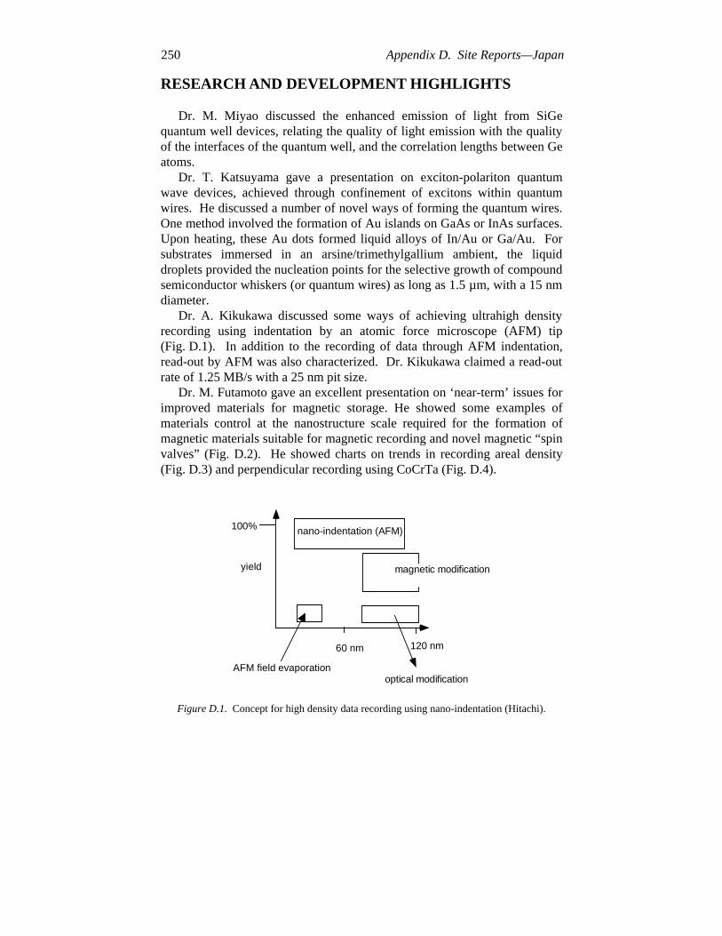
Dr. A. Kikukawa discussed some ways of achieving ultrahigh densityrecording using indentation by an atomic force microscope (AFM) tip(Fig. D.1). In addition to the recording of data through AFM indentation,read-out by AFM was also characterized. Dr. Kikukawa claimed a read-outrate of 1.25 MB/s with a 25 nm pit size.
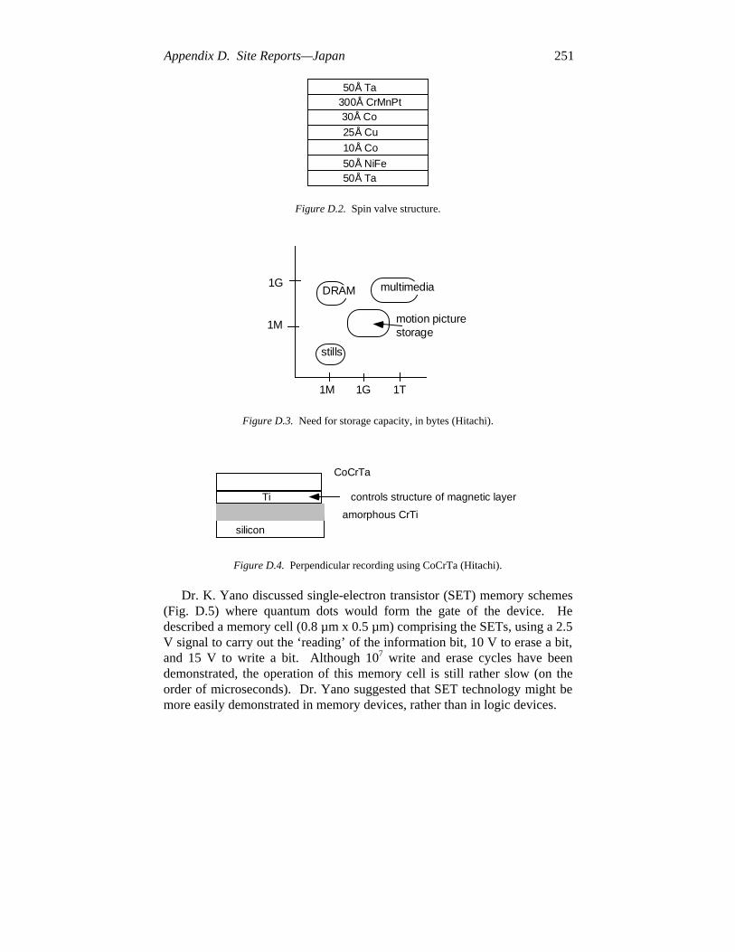
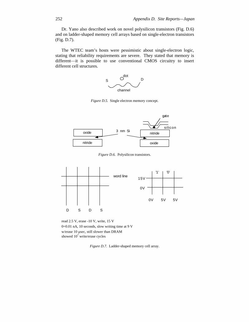
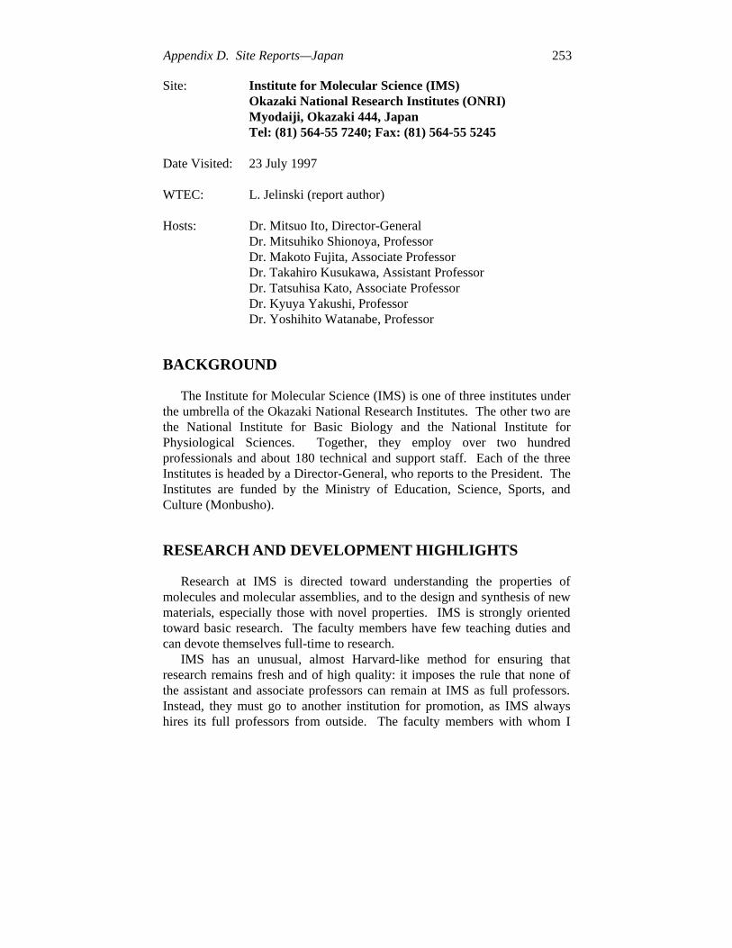
Dr. M. Futamoto gave an excellent presentation on ‘near-term’ issues forimproved materials for magnetic storage. He showed some examples ofmaterials control at the nanostructure scale required for the formation ofmagnetic materials suitable for magnetic recording and novel magnetic “spinvalves” (Fig. D.2). He showed charts on trends in recording areal density(Fig. D.3) and perpendicular recording using CoCrTa (Fig. D.4).
nano-indentation (AFM)100%
optical modification
magnetic modificationyield
120 nm60 nm
AFM field evaporation
Figure D.1. Concept for high density data recording using nano-indentation (Hitachi).
Appendix D. Site Reports—Japan 251
50Å Ta
50Å Ta
30Å Co
25Å Cu
10Å Co
50Å NiFe
300Å CrMnPt
Figure D.2. Spin valve structure.
1G
1M
1M 1T1G
multimediaDRAM
motion picturestorage
stills
Figure D.3. Need for storage capacity, in bytes (Hitachi).
silicon
amorphous CrTi
Ti
CoCrTa
controls structure of magnetic layer
Figure D.4. Perpendicular recording using CoCrTa (Hitachi).
Dr. K. Yano discussed single-electron transistor (SET) memory schemes(Fig. D.5) where quantum dots would form the gate of the device. Hedescribed a memory cell (0.8 µm x 0.5 µm) comprising the SETs, using a 2.5V signal to carry out the ‘reading’ of the information bit, 10 V to erase a bit,and 15 V to write a bit. Although 107 write and erase cycles have beendemonstrated, the operation of this memory cell is still rather slow (on theorder of microseconds). Dr. Yano suggested that SET technology might bemore easily demonstrated in memory devices, rather than in logic devices.
252 Appendix D. Site Reports—Japan
Dr. Yano also described work on novel polysilicon transistors (Fig. D.6)and on ladder-shaped memory cell arrays based on single-electron transistors(Fig. D.7).
The WTEC team’s hosts were pessimistic about single-electron logic,stating that reliability requirements are severe. They stated that memory isdifferent—it is possible to use conventional CMOS circuitry to insertdifferent cell structures.
S Ddot
channel
Figure D.5. Single electron memory concept.
nitride
oxide nitride
oxide
3 nm S i
gate
s i l icon
Figure D.6. Polysilicon transistors.
D S D S
word line
read 2.5 V, erase -10 V, write, 15 V
0=0.01 nA, 10 seconds, slow writing time at 9 V
w/erase 10 µsec, still slower than DRAMshowed 107 write/erase cycles
Figure D.7. Ladder-shaped memory cell array.
15V
0V
0V 5V5V
’1’ ’0’
Appendix D. Site Reports—Japan 253
Site: Institute for Molecular Science (IMS)Okazaki National Research Institutes (ONRI)Myodaiji, Okazaki 444, JapanTel: (81) 564-55 7240; Fax: (81) 564-55 5245
Date Visited: 23 July 1997
WTEC: L. Jelinski (report author)
Hosts: Dr. Mitsuo Ito, Director-GeneralDr. Mitsuhiko Shionoya, ProfessorDr. Makoto Fujita, Associate ProfessorDr. Takahiro Kusukawa, Assistant ProfessorDr. Tatsuhisa Kato, Associate ProfessorDr. Kyuya Yakushi, ProfessorDr. Yoshihito Watanabe, Professor
BACKGROUND
The Institute for Molecular Science (IMS) is one of three institutes underthe umbrella of the Okazaki National Research Institutes. The other two arethe National Institute for Basic Biology and the National Institute forPhysiological Sciences. Together, they employ over two hundredprofessionals and about 180 technical and support staff. Each of the threeInstitutes is headed by a Director-General, who reports to the President. TheInstitutes are funded by the Ministry of Education, Science, Sports, andCulture (Monbusho).
RESEARCH AND DEVELOPMENT HIGHLIGHTS
Research at IMS is directed toward understanding the properties ofmolecules and molecular assemblies, and to the design and synthesis of newmaterials, especially those with novel properties. IMS is strongly orientedtoward basic research. The faculty members have few teaching duties andcan devote themselves full-time to research.
IMS has an unusual, almost Harvard-like method for ensuring thatresearch remains fresh and of high quality: it imposes the rule that none ofthe assistant and associate professors can remain at IMS as full professors.Instead, they must go to another institution for promotion, as IMS alwayshires its full professors from outside. The faculty members with whom I

254 Appendix D. Site Reports—Japan
spoke, including junior professors, thought that this policy worked quitewell.
Research at IMS that falls within the scope of this report is in the generalcategory of synthesis of novel materials, some with inspiration from biologyand some with biomolecules as the building blocks. Most of the work thatinvolves nanoparticles involves some form of organometallic chemistry.The hallmarks of the research are two-fold: creativity, and the soundness bywhich the new materials are characterized and evaluated. Much of theresearch the WTEC team saw on this visit has been published in high qualityjournals such as Nature and the Journal of the American Chemical Society,attesting to the international reputation of IMS and the high quality of theresearch. Several of the faculty members have good collaborations withother scientists in Japan. One has an ongoing and productive NSF-fundedcollaboration with the University of Rochester, and another introduced thevisiting WTEC team member to a visiting researcher, on leave from EmoryUniversity, who was spending six months in his lab.
Japan seems to be in a leadership role in the production ofmetallofullerenes. IMS has a large-scale facility for producing fullerenes,and Prof. Kato has been successful in producing C82 that contains Sc, Y, andLa inside the cage structure. Kato is now using the metal inside the fullereneas a way to “tune” the reactivity of the outside. For example, he has shownhow LaC82 can be reacted with disilanes and diazo compounds to formadducts. A combination of electron spin resonance (ESR) and theory isbeing used to explain the reactivity of the precursor and the productsobtained. One could imagine how this ground-up assembly of nanomaterialscould be polymerized to produce larger molecules with novel properties.
Another area of research involves the characterization of magnetictransport and optical properties in phthallocyanines (Pc). Of special interestis PtPc(AsF6)0.5, whose transport properties are being studied under highpressure.
Prof. Shionoya, a very young full Professor who recently came to IMSfrom Hiroshima University, is using novel combinations of DNA, metalligands, DNA templating, and proteins to produce molecular wires andmolecular hoops through which DNA could be threaded. He is also usingdouble-stranded peptides whose helix pitch could be controlled by anentrained copper that could be induced to go from Cu(I)tetrahedral toCu(II)square planar , perhaps by electrons delivered by an STM tip. Figure 7.6(p. 123) summarizes Prof. Shionoya’s vision of how bioinspiration could beused to produce nanodevices.
In a very creative and careful series of single point mutations, Prof.Watanabe has uncovered evidence for, and verified the existence of a “push-pull” mechanism for cytochrome C peroxidase. This was done by drawing

Appendix D. Site Reports—Japan 255
an analogy between peroxidase and cytochrome P-450, and using insightsgleaned from similarities in the active site.
Finally, Prof. Fujita’s work involves the approach of using self-assemblyby transition metals to form organized large structures. He has been able tomake various nanocages, which have potential applications for controlleddrug release. He has also used three-dimensional organometallic cagecompounds to achieve a “ship-in-a-bottle” synthesis of organic moleculesand is currently producing nanostructured molecules with larger cavities thanhave ever been made before.

256 Appendix D. Site Reports—Japan
Site: Joint Research Center for Atom Technology (JRCAT)Angstrom Technology Partnership (ATP)c/o National Institute for Advanced Interdisciplinary
Research1-1-4 Higashi, Tsukuba, Ibaraki 305, JapanTel: (81) 298-54 2570; Fax: (81) 298-54 2575
Date Visited: 22 July 1997
WTEC: R.W. Siegel (report author), D.M. Cox, H. Goronkin,J. Mendel, H. Morishita, M.C. Roco
Host: Dr. Eiichi Maruyama, Executive Director and GeneralDirector of Research CenterE-mail: [email protected]
BACKGROUND
Tuesday morning 9:30 to 12:00 noon of 22 July was spent in Tsukubavisiting the Joint Research Center for Atom Technology (JRCAT), anorganization founded in February of 1993 through a joint contract betweenthe National Institute for Advanced Interdisciplinary Research (NAIR) andthe Angstrom Technology Partnership (ATP). These latter organizationswere created by the Agency of Industrial Science and Technology (AIST) ofthe Ministry of International Trade and Industry (MITI). The central focusof JRCAT is the Atom Technology Project, a ten-year effort begun by AISTin fiscal year 1992 as one of its Industrial Science and Technology FrontierPrograms under the official title, Research and Development of UltimateManipulation of Atoms and Molecules. AIST’s total ten-year budget for thisproject is about ¥25 billion (~ $250 million), which flows mostly (~ 90%)through the New Energy and Industrial Technology DevelopmentOrganization (NEDO) and hence ATP, with the balance (~ 10%) flowingdirectly through NAIR. The distinct advantage of this imbalance for JRCATis that the NAIR funds are hard (national) monies that cannot be used forhiring people, while the ATP funds are soft (invested) monies that can beused very flexibly. The Atom Technology Project is envisioned ascomprised of overlapping efforts in atom manipulation, nanoscale self-organization, and critical-state phase control based on in situ dynamicmeasurement and control complemented by ab initio calculation.
The WTEC panel visit was hosted by Dr. Eiichi Maruyama, ExecutiveDirector of ATP and the Atom Technology Project Leader, who presented a
Appendix D. Site Reports—Japan 257
very informative and extensive introduction to JRCAT and its researchefforts. JRCAT presently has 36 administrators and about 100 researchscientists, of whom 35 are from industry, 28 are from national laboratories, 7are from universities, 26 are postdocs, and four are PhD candidates. About60% of the scientific staff are supported from ATP and 40% from NAIR. Ofthese, there are 78 PhDs, 21 foreign scientists, and 3 female scientists. Thetotal funding flow has been reasonably steady since FY1995 at about ¥2.5billion per annum, with significant fluctuations in the first three years forinitial capital expenditures. The publication of research results in “major”journals (i.e., those with high citation impact factors, such as Nature,Science, Physical Review Letters, Applied Physics Letters, and PhysicalReview B) appears to be used as a measure of research program success.There have been a significant number of such publications (~ 120 per year)from JRCAT during FY94-FY96.
RESEARCH AND DEVELOPMENT HIGHLIGHTS
The Atom Technology Project research program is lead by ProjectLeader E. Maruyama along with Deputy Project Leaders K. Tanaka(experiment) and K. Terakura (theory) and is organized into 11 groups infour general areas. These are as follows (with leader):
Solid Surface and Solid Material
• Measurement and control of atomic level structures by mechanicalprobe—19 scientists (H. Tokumoto)
• Observation and formation of atomic scale structure using beamtechnology—8 scientists (M. Ichikawa)
• Measurement and control of surface reactions for nanostructurefabrication—7 scientists (M. Ozeki)
• Atomic level analysis and control of II-VI semiconductor surface—6scientists (T. Yao)
• Exploration of transition metal oxides and organic molecular system—8scientists (Y. Tokura)
• Exploration of amorphous semiconductors, magnetic thin films, solid-liquid interfaces—15 scientists (K. Tanaka)
Cluster in Free Space
• Formation and control of clusters in ion trap and on solid surface—4scientists (T. Kanayama)

258 Appendix D. Site Reports—Japan
Organic Molecular Structure
• Scanning probe microscopy (SPM) and optical analysis for DNA andorganic molecular structure—11 scientists (T. Okada)
Quantum Simulation of Atomic and Molecular Processes
18 scientists are working on several programs, including the following:
• Organic molecular system, new techniques for computer simulation (K.Terakura)
• Semiconductor materials (T. Uda)The theory group is also responsible for the JRCAT Supercomputer
Laboratory, introduced in March 1994.Formal evaluation of the research program is held only at its midpoint
(six years) and end (ten years), but annual reports are produced. Successfulefforts are expected to be transferred to industry. Some projects arecontinued under new programs, and others are terminated after theseevaluations. The second phase (next 4 years) of JRCAT will see increasedcollaboration with industry, a new study on spin-electronics applications,and an effort to maintain top-level atom technology. The primary scope ofthe Atom Technology Project will continue to include nanostructureformation and control of surfaces and interfaces (especially in semiconductorand related materials); spin electronics (new materials and measurements);observation and manipulation of atoms and clusters; and theoreticalsimulation (emphasizing good interaction with experimental groups).
In carrying out its mission, JRCAT interacts with foreign universities viacontact and exchange of scientists (e.g., with the University of Birminghamin the UK). Also, the science and technology laws in Japan were changedca. 1995 to allow Japanese university professors to have more significantinteraction with JRCAT and other industries.
The WTEC panel also made visits to four JRCAT research laboratories,the Advanced Interdisciplinary Laboratories of Drs. K. Tanaka, K. Ichikawa(H. Watanabe, host) and Y. Tokura (A. Asamitsu, host), and the TheoreticalResearch Laboratory of Dr. K. Terakura. The group of Dr. H. Tokumotowas unfortunately away at a conference that day; it is active in attempts tocreate nanoscale ferroelectric domains by scanning force microscopy (SFM)for nonvolatile, high density memories, sensors and actuators, but is mainlyworking at the micron scale at present. It also works on self-assembledmonolayers (SAM) on surfaces, particularly those that are electricallyconductive. All of the groups are extremely well equipped with all of thelatest facilities and capabilities necessary to carry out their respectivemissions.
Appendix D. Site Reports—Japan 259
The Tanaka group laboratory is located in a specially vibration-isolatedseparate building in the NAIR facilities. The primary research themes of thisgroup are (1) fabrication of semiconductor nanostructures and investigationof their defect structure, (2) creation of magnetic superstructures andsearching for new magnetic materials, and (3) elucidation atatomic/molecular levels of the electric double layer at solid-liquid interfaces.Work is ongoing in developing high resolution Raman spectroscopy for thestudy of molecules on surfaces. It was reported that information fromindividual molecules can be obtained by coupling to surface plasmonpolarization, which enhances the signal by three orders of magnitude. Also,atom manipulation (atom and layer removal) by scanning tunnelingmicroscope (STM) tips is being carried out on Si (mainly) and hightemperature superconductors in a UHV-STM without damaging thesurrounding regions.
The Ichikawa group has as its primary research themes (1) developmentof an atomic manipulation system using beam technology and extremelyhigh vacuum pumping, (2) development of surface/interface characterizationtechnologies, and (3) exploration of surface/interface reactions useful fornanostructure formation. The laboratory contained a state-of-the-art 30 keVUHV field-emission scanning electron microscope (SEM) with an SPMbeing used for Si-based nanostructures. For this development project, aunique STM with atomic resolution was developed on a 6-axis manipulatorin the UHV-FE-SEM, but because of unique problems with vibrationisolation, the system requires a special isolation room. Electron holographyusing a biprism to produce 2 coherent beams from the FE (field emission)gun was also in place on the SEM and was being used to create nanoperiodicstructures (with 17 nm wavelengths) on SiO2. In another major developmentproject, a multifunctional Surface Analysis System, with Auger analysis witha 1.4 nm diameter beam probe, was built in this group. About $2.5 millionwas spent on each of these two major development projects.
The Tokura group (also partly at the University of Tokyo) focuses on thesynthesis and physics of oxide electronic materials and organic molecularsystems. Examples of current work are the floating-zone crystal growth, in aparabolic mirror image furnace (manufactured by NEC), of large singlecrystals (e.g., Pr0.65Cu0.35MnO3); investigation of natural one-dimensionallymodulated nanostructured superlattices (….+ insulating + magnetic+ insulating +....) for giant or colossal magnetoresistance (GMR or CMR)applications; and studies of electric-field-induced resistivity changes in.… + insulating + metallic + insulating + metallic + .... multilayers, such asPr1-xCaxMnO3 (e.g., x = 0.3), below 100 K. A main focus of the group’sresearch is using laser ablation to build layers by cluster assembly onstepped substrates of SrTiO3 for functional device applications. A system
260 Appendix D. Site Reports—Japan
with five movable targets and a fixed laser is being used for this work, andthe studies are carried out as a function of substrate temperature and oxygenpartial pressure.
Finally, the WTEC team visited the Terakura theory group, led by Dr.Kiyoyuki Terakura, who has been at JRCAT for about three and a half years.This world-class theory group specializes in first-principles, state-of-the-artquantum simulations of atomic and molecular processes in the areas ofsemiconductor surfaces, transition metal compounds, and exotic materialssuch as conducting organic solids (e.g., DCNQI-M, with M = Li, Ag, Cu).The group also develops new computational methodologies for approachingsuch problems and is responsible for the large-scale supercomputer system atJRCAT, consisting of two main computers—a vector-parallel computer(VPP500/32) and a massively parallel computer (128 node CM-5E). Thetheory group has good interactions with the experimental efforts at JRCAT;although frequently the experimentally investigated systems can be rathercomplex for fundamental theoretical simulation, serious theoretical effortsare made to benefit the experimental program. The Terakura group also hasextensive external collaborations with NEC, Hitachi, Fujitsu, and variousuniversities in Japan and abroad. In addition to its normal publications, thetheory group disseminates the results of its efforts in a series of well-prepared annual reports.
Appendix D. Site Reports—Japan 261
Site: Kyoto UniversityGraduate School of Energy ScienceYoshida, Sakyo-kuKyoto 606-01, JapanFax: (81) 75-753 5464
Date Visited: 25 July 1997
WTEC: C. Koch (report author), D.M. Cox, J. Mendel, H. Morishita,R.W. Siegel
Host: Professor Paul Hideo Shingu, Dean
BACKGROUND
This visit concentrated on the laboratory of one professor, Professor PaulHideo Shingu at Kyoto University. He has a group of associates andgraduate students (about 15) and is funded by the Ministry of Education,Science, Sports, and Culture (Monbusho).
RESEARCH AND DEVELOPMENT HIGHLIGHTS
Professor Paul Hideo Shingu was the WTEC panel’s host. He is theDean of the Graduate School of Energy Science at Kyoto University. He is apioneer in the use of severe mechanical deformation to producenanocrystalline (nc) microstructures. He was the first researcher todemonstrate the synthesis of nc materials by mechanical alloying (highenergy ball milling) in the Ag-Fe immiscible system in a paper published in1988. His group was the first to point out that nc materials can be made byMA. Much of his group’s work in this area is summarized in a paper byP.H. Shiugu in Materials Transactions JIM 36:96 (1995). In order to bebetter able to define the mechanism(s) involved in creation of nc materialsby severe plastic deformation, Prof. Shungu turned to the method of repeatedpress-rolling of component foils or powder mixtures. This “deterministic”mechanical alloying has allowed for both experimental studies of thedeveloping microstructure—by, for example, high resolution transmissionelectron microscopy (HRTEM)—and the modeling of the microstructure bycomputer simulations. He and his coworker, Dr. K.N. Ishihara, have usedchaos theory to model the microstructure obtained in shearing of dissimilarcomponents, based on several simple approaches such as the baker’stransformation, linear shear, and parabolic shear. The iteration of certain
262 Appendix D. Site Reports—Japan
mapping generates chaos. It is noted that the application of preciselydeterministic mapping can generate a chaotic mixing of initiallymacroscopically separated structures by a surprisingly small number ofrepeated applications of a mapping. This is analogous to the structuresobserved experimentally due to the mechanical deformation.
Among the systems Shingu’s group has studied are immiscible systemssuch as Ag-Cu and Cu-Fe, which form metastable solid solutions; Ag-Fe,which forms an nc composite microstructure; and Co-Cu, which exhibits thegiant magnetoresistance (GMR) effect.
The preparation of multilayers by repeated rolling requires carefulcontrol of the process. Component foils (or powder compacts) are firstannealed in vacuum, pressed together in vacuum, annealed, then repeatedlyrolled and annealed. The selected annealing temperature is critical tomaintaining the planarity of the layers and to avoid their spheroidization,while relieving the deformation strains to allow further rolling.
HRTEM of the layered structures reveals nc grains within the layers, withrotation of the grain into an apparent epitaxial relationship with the othercomponent.
The panel’s other observations on this visit include the following:• the rolling of mixed powder compacts has produced results similar to
those with foils• a number of mechanical and magnetic measurements have been made on
these samples• it is believed this method of repeated rolling could be scaled up to
commercial quantities, since rolling technology is well developed in thesteel industry, as one example
• Shingu’s group consists of several professionals, one technician, and15-20 graduate studentsA tour of the laboratory facilities revealed several critical processing
devices such as a pseudo hot isostatic press (HIP), a good four-high rollingmill, and a vacuum hot press. Characterization facilities, such as atransmission electron microscope, are shared with others in the Department.
Professor Shingu’s research differs in the smaller scale of his effort fromthat carried on by the large groups at national laboratories and IMR at TohokuUniversity. However, the innovative and creative studies done in his grouphave made significant contributions to the field of nanostructured materials.
REFERENCE
See also Yasuna et al. 1997. J. Appl. Phys. 82(5):2435-2438.
Appendix D. Site Reports—Japan 263
Site: Nagoya UniversityDepartment of Crystalline Materials ScienceFurocho, Chikusa-kuNagoya 464-01, JapanFax: (81)-52-789-3821
Date Visited: 25 July 1997
WTEC: D. Shaw (report author), E. Hu, L. Jelinski, M.C. Roco,C. Uyehara
Hosts: Professor Uichiro MizutaniProfessor Toshiharu FukunagaProfessor Nobuo TanakaProfessor Jun-ichiro Inoue
RESEARCH AND DEVELOPMENT HIGHLIGHTS
Professor Toshiharu Fukunaga, Nanoparticles byMechanical Milling
The X-ray diffraction spectrum of milled graphite was the same as foramorphous material. The density decreased from 2.2 to 1.85 g/cm3 in 36hours of milling. Neutron diffraction confirmed the disorder. These resultswere analyzed to calculate the radial distribution factor that gives thecoordination number, which reduced from 3.01 to 2.82 in the 36 hours. It isbelieved that this describes production of dangling bonds in the milledmaterial. Assuming the crystalline structure is unchanged upon milling, onlythe size of the particles changes and the coordination number decreases. Thesize was estimated to be about 27 Å.
Transmission electron microscopy (TEM) before milling showed alayered graphite-like structure. After milling the material was amorphous.
Ball milling is done at low temperature. The equipment has a 150 G (xgravity) capability but 10 G is used in work in this department.
Trigonal selenium was also milled. Using the same analytical proceduresas above, it was estimated that the particles contained about 22 atoms.
Li and graphite were milled together. The Li incorporates into thegraphite and coats the balls to produce a gold-colored LiC6 film. The Li isinserted into the hexagonal C network if the milling intensity is kept low.The potential application is to batteries. One of the technical challenges is toremove the material from the balls.
264 Appendix D. Site Reports—Japan
Professor Nobuo Tanaka, Electron Microscopy
Prof. Tanaka described nanobeam drilling using e-beam, which showedapproximately 1 nm square windows drilled with a cylindrical beam. Thelattice was distorted around the periphery of the window.
Tanaka discussed a number of other issues, including granularmagnetoresistive structures and mass production of fine particles, but it wasnot clear whether the work was done at Nagoya University or pulled fromthe literature.
Tanaka showed a video of two sharp gold tips coming together to create aliquid-like interface. The tips were electrolytically sharpened. As seen inthe video, the tip diameter was about 10-15 atoms. As the tips separated, theliquid-like region took on the lattice constant of one of the two tips.Previously, this demonstration had been reported with a tip and a flatsurface.
Professor Jun-Ichiro Inoue, Transport Phenomena inMacroscopic Magnets
Prof. Inoue has calculated the magnetoresistance ratio vs. surface/volumeratio of FeCr granules in a matrix. The model was independent of matrixmaterial and distance between clusters. Although the assumed spacing was2-5 Å, interactions were not included. Data from Tohoku University of atunnel diode with Co-AlO granular barrier had a four order of magnitudedrop in resistivity and a constant MR ratio of about 19% at 4.2 K. Thebarrier thickness was about 1.0 µm, and the maximum voltage was 1.0 V.Typical barrier thickness reported in the literature is about 10-15 Å, so theTohoku data applies to fields that are about 1E7 lower than structuresdesigned for memory cells or hard drive heads.
The decrease in resistivity was explained by the charging energy of thesingle-electron-like granules, although this explanation seems unlikely tothis author.
Appendix D. Site Reports—Japan 265
Site: National Institute for Advanced InterdisciplinaryResearch (NAIR)
Cluster Science Group1-1-4 HigashiTsukuba, Ibaraki 305, JapanTel: (81) 298-54 2540; Fax: (81) 298-54 2949
Date Visited: 23 July 1997
WTEC: D.M. Cox (report author), H. Goronkin, E. Hu, J. Mendel,H. Morishita
Host: Dr. Harutoshi Takeo, Leader of Cluster Science GroupE-mail: [email protected]
BACKGROUND
NAIR, the National Institute for Advanced Interdisciplinary Research isone of 15 research institutions of AIST, the Agency of Industrial Science andTechnology. The focus of the AIST laboratories is concentrated on R&Dprograms judged to be capable of raising the level of Japan’s technology infour main ways:1. nurture new leading-edge technology that will lay the basis for future
technical innovation2. establish basic technical standards3. meet the society’s needs for earthquake prediction, pollution prevention,
and environmental preservation4. embrace all basic or general research that is appropriate for a national
research organizationNAIR was founded in January 1993 with an objective of pursuing
interdisciplinary research themes covering fundamental and frontier areas ofindustrial science. The institute is dedicated to the creation of internationalintellectual properties in broad fields of basic and strategic R&D, wherenational funds are expected to play a positive role. NAIR is characterized bythe tripartite collaboration of industrial, academic, and governmental sectors,as well as by international cooperation. It is portrayed as an innovativeattempt to overcome institutional boundaries by bringing together scientistsof diversified specialty—not only from research institutes under AIST andthe Science and Technology Agency (STA), but also from universities andresearch organizations in the private sector—to engage in intensive jointresearch.
266 Appendix D. Site Reports—Japan
RESEARCH AND DEVELOPMENT HIGHLIGHTS
NAIR had four main research projects at the time of the WTEC visit:1. The Atom Technology Project. This project has as its goal the ultimate
technology for manipulating atoms and molecules; it started in January1993 and runs until March 2002; total budget is ¥25 billion.
2. Research on Cluster Science Project. The goal of this project wasexperimental and analysis of the character of clusters; it ran from January1993 until March 1998; total budget was ¥1 billion.
3. Research on Bionic Design Project. The goal of this project was toadvance understanding in cell and tissue engineering and molecularmachines; it ran from January 1993 until March 1998; total budget was¥1 billion.
4. Basic Research on Next Generation Optoelectronics. The goal of thisproject is large capacity optical memory; this is a new program with seedmoney first available in April 1996; start date appeared to be April 1998,running until March 2003; total budget in April 1996 was ¥80 million fordefining program goals and directions.In addition to the above projects, NAIR has carried out several two- to
three-year feasibility studies since its formation in 1993. The AtomTechnology Project is the subject of a separate review in the JRCAT sitereport (p. 256 of Appendix D). The remainder of this report will focus onthe Research on Cluster Science Project.
Research on Cluster Science
Dr. Harutoshi Takeo, the Cluster Science Group Leader, greeted theWTEC panel and first presented an overview of the science projects in hisgroup, then led the panel on a tour of the laboratories. The cluster groupconsists of about 30 researchers, with nine regular research staff members,seven staff members on assignment from other AIST institutes, one from auniversity, 9-11 postdoctoral fellows, of which seven or eight are foreigners,and two to three graduate students. To further broaden the perspectives ofthe Cluster Science Group, it organizes a yearly workshop to which it invites15-20 outside researchers. Over the lifetime of the project over 90 outsidescientists will have participated in and contributed to these workshops.
The Cluster Science Group’s research areas fall roughly into four areas:1. clusters in collisionless environments (molecular beams)2. clusters in liquid or solution3. clusters stabilized on surfaces or in matrices4. clusters stabilized in a nanocage such as a zeolite

Appendix D. Site Reports—Japan 267
In the collisionless environment the main activities are focused onprobing the structure and reactivity of clusters under single collisionconditions. The research facilities, which have been designed and builtentirely from scratch since mid-1993, include a Fourier transform ioncyclotron resonance mass spectrometer with which cluster structures arestudied via laser spectroscopy; cluster chemical reactivity is being probedthrough controlled introduction of various molecular species. A secondapparatus, a cluster beam system, combines infrared pumping of molecularadsorption on clusters with resonantly enhanced multiphoton ionizationtechniques to interrogate cluster and molecular bonding. Bonding of anilineand aniline dimers to a variety of different molecules has been studied.
To study the properties of liquid clusters, an expansion liquid dropletsource together with a time-of-flight mass spectrometer (reflectron mode)was built. Study of mixtures of water/ethanol solutions have shown anevolution from clusters consisting of mostly water molecules complexedwith one or two ethanol molecules for high concentration of water in themixture, to clusters consisting of mostly ethanol molecules complexed withone or two water molecules when the ethanol concentration in the mixturereaches 40% or more. Such studies allow fundamental intermolecularinteractions of molecules in liquids to be investigated.
To probe the properties of clusters on supports, several sophisticatedpieces of experimental apparatus were built. One especially impressiveexperiment uses a liquid metal source (heated crucible) to produce clustersthat are deposited on a cryogenic substrate in order to stabilize them. Theapparatus is interfaced with an X-ray source. The substrate with differentcluster deposits is rotated in-situ, allowing X-ray determination of thestructure to be investigated as a function of the metal type, the cluster size,the substrate material, and the temperature. Interestingly, gold clusters withsize < 6 nm are found to have icosahedral structure and not the fcc structureof bulk gold. Upon warming the substrate, the clusters sinter and thedevelopment of the fcc structure can be followed as a function oftemperature. Studies of gold-copper alloy clusters also show icosahedralstructure for clusters less than about 6 nm. Several other metal and metalalloy systems will be examined.
To investigate the quantum properties of nanometer-sized materials, theCluster Science Group is attempting to stabilize metal clusters in thechannels of zeolites. Specifically they have put sodium into the channels ofan LTA zeolite in the hopes of producing a quantum wire. The sodium-doped materials have been shown to exhibit photochromic behavior,exhibiting reversible darkening upon exposure to light. In contrast,potassium-doped zeolites investigated by another group exhibitedferromagnetic behavior.

268 Appendix D. Site Reports—Japan
One of the researchers has developed a terahertz spectrometer capable ofprobing molecular vibrations in the 15-30 cm-1 range. At the time of theWTEC visit, this spectrometer appeared ready to be applied to real problems.
CONCLUDING REMARKS
In the short time it has existed, the NAIR cluster group has put togethersome of the best approaches of any group in Japan to study fundamentalscience issues. They began with virtually no equipment in 1993 and havedesigned and built a series of sophisticated apparatuses, each focused onprobing a specific fundamental issue of cluster science. The unfortunateevent was the termination of this effort in March of 1998. In this particularinstance, the researchers are just beginning to harvest the results of carefuland thoughtful design of state-of-the-art equipment. In at least one instancethe apparatus was just coming on line at the time of the panel’s visit, and thatparticular scientist will have only a few months to generate data beforetermination of the program.
It was the WTEC panel’s perception that several of the researchers(almost all fairly young) did not yet have positions to which they couldmove. Some of the older researchers obviously will be able to return to theirsending organization, but several were hired directly into this project andhad no ties to any outside organization. We were informed that eachresearcher will be allowed to keep his equipment in the new position, whichis certainly good news, but “the termination of the program” was a themethat had certainly raised the anxiety level of many of the staff. The qualityof the research and the novelty with which these young researchers haveapproached science could serve as a model for other groups in Japan;namely, the researchers were allowed (even encouraged) to identifyinteresting cluster science problems and then design experimental apparatusto probe these problems, rather than to just buy equipment. This appears tohave born fruit, but the fruit may dry up before harvest can occur.
Appendix D. Site Reports—Japan 269
Site: NECElectron Devices Laboratory34 MiyugaokaTsukuba, Ibaraki 305, JapanFax: (81) 298-56 6135
Date Visited: 23 July 1997
WTEC: H. Goronkin (report author), D. Cox, J. Mendel,H. Morishita, M.C. Roco, R.W. Siegel
Hosts: Dr. Kohroh Kobayashi, General Manager, FundamentalResearch Laboratories
Dr. Jun’ichi Sone, Senior Manager, Advanced DeviceResearch Lab
Dr. Y. Ochiai, Manager, Advanced Device Research LabDr. K. Tanaguchi, Manager, Exploratory Research Lab
BACKGROUND
Funding: 1% of NEC’s sales go to its Corporate Research Laboratory(including the Fundamental Research Laboratories)
70% of funding is from the corporate level30% is contract funding from business groups15% of funding for Fundamental Research Laboratories is
from business groups and national projects
Targeting: Business group R&D, from three to five yearsFundamental R&D Labs, from five to ten years
Staffing and Tsukuba: 300 (devices, materials, fundamental orientation)Foci of NEC Kawasaki: 1,100 (computer and communication systems,Labs: software, and components)
Princeton: 50-60 (computer science and physical science)Berlin, Bonn: (computers and communications software for
parallel computers and ATM transmission technologies)
270 Appendix D. Site Reports—Japan
RESEARCH AND DEVELOPMENT HIGHLIGHTS
K. Taniguchi—Si, Ge, C Clusters
• the Exploratory Research Lab has synthesized buckyball magic numbersof 20, 24, 46, and 60 and has achieved >100
• change bonding from van der Walls to covalent by changing number ofatoms in the ball
• doping provides conductivity and superconductivity• need ionized Si or Ge; quench to remove electron and form 20 or 24 atom
cages• modify substrate to form clusters by adding electrons by doping, ion
implantation, e-beam• critical temperature for silicon cages is 6-8 K
Y. Ochiai—Nanofabrication
The Goal of the Advanced Devices Research Lab is 10 nm scalelithography using e-beam. It needs a capability by 2007 for manufacturing16 Gbit DRAMs. Previous work on short gates includes 100 nm in 1987, 45nm in 1993 using a 50 keV field emitter beam having less than 5 nm beamdiameter at 100 pA; and 40 nm in 1997.
The lab is using Tox = 3.5 nm and is working on 1 nm SiO2. Althoughtunneling will exist, it is believed that the small area of the gate oxide willlimit gate current to a negligible fraction of the channel current.
W/L scaling is not maintained at 2:1.The lab developed an e-beam resist (Calixarene, molecular weight 1,000)
for the 10 nm project in which resolution is limited by the six benzene ringlength to 6 nm; 10 nm lines show smooth edges and regular spaces. Theresist was licensed to other companies for commercialization.
Atom Beam Holography
Starting with a Ne discharge, the neon momentum is decreased and theatoms are trapped in a laser beam. The Ne atoms are allowed to fall undergravitational attraction and they pass through a hologram plate beforedropping onto a microchannel plate, where they excite an image. The largemass of Ne compared to electrons provides a large increase in resolution.According to quantum mechanics, the wave of a single Ne atom can passthrough thousands of holographic channels simultaneously where it isdiffracted and then recombined to form images on the microchannel plate. It
Appendix D. Site Reports—Japan 271
is hoped that this can be used for future 1 nm lithography. It currently takesseven hours to form an image. This project began in 1995 in collaborationwith the University of Tokyo.
Jun’ichi Sone—Nanoelectronics
Encouraged by Advanced Device Lab’s success with e-beam lithographyusing Calixarene resists to obtain 10 nm features, various device structuresbecome possible. The Lab’s goal is to look for the classical-quantumcrossover in MOSFET structures. There are many potential problems,including source-drain tunneling (S-D) and tunneling through the gateinsulator. An EJ MOSFET (electrically variable junction MOSFET) wasfabricated with gate lengths from 134 nm to 32 nm. A second gate locatedover the channel control gate was used to modulate the resistance of thesource and drain virtual access regions. Satisfactory saturatingcharacteristics were obtained down to 32 nm. At 32 nm, short channeleffects were observed; however, no S-D tunneling was observed. At thiswriting, a 15 nm gate was achieved but results were not reported. It is hopedthat when quantum effects are observed, useful novel devices can be made.
The advanced e-beam lithography with PMMA resist was used tofabricate a metallic single-electron transistor using Al/Al2O3/Alisland/Al2O3/Al. The process involves opening a 20 nm window betweensource and drain. The Al is oxidided to form Al2O3 , and Al is deposited inthe window to form the island region. Extremely reproducible drain currentpeaks as a function of gate voltage were obtained. Unlike semiconductorSETs, for example, where the peaks are of uneven height, the lack ofdepletion and charging of defects provides uniform heights in the metallicsystem. It is believed that 10 nm islands could provide room temperatureoperation.
CONCLUDING REMARKS
NEC’s Electron Devices Laboratory is one of the top labs in the world innanoelectronics. This lab seems to be able to quickly start new programs inpromising areas and to change direction when fundamental obstacles blockthe path to progress. The Atom Beam Holography and the 10 nm gateprojects are at the leading edge. The lab appears to be clear in itsunderstanding of how its research fits into future company needs and howthe research must be directed to produce world-leading results.
272 Appendix D. Site Reports—Japan
Site: National Industrial Research Institute of Nagoya (NIRIN)1 Chome Hirate, KitakuNagoya 462, JapanFax: (81) 52911 1661
Date Visited: 25 July 1997
WTEC: J. Mendel (report author), D.M. Cox, C. Koch, H. Morishita,R.W. Siegel
Hosts: Dr. Shuzo Kanzaki, Chief Senior ResearcherDr. Mutsuo Sando, Research ManagerDr. Sakae Tanemura
BACKGROUND
The National Industrial Research Institute of Nagoya (NIRIN) has as itsmission to carry out advanced materials research on ceramics, metals,composites, and related materials. Established in 1952, its main researchfield is material science and technology. There is close cooperation withdomestic and global universities; there are also efforts to interface with othernational research institutes.
Within Japan’s National Industrial Research Institutes (NIRI) there aresix major technical departments. In 1996, the annual budget for NIRI was$92 million (US). Total staff is 220 who participate in the Institute. For thisvisit, the WTEC panel focused on the area of synergy ceramics andmaterials.
In the area of synergy ceramics, the emphasis is on structural control forimproving a specific property of a given material. Here there is effort tosimultaneously control structural elements at every stage (from atomic scaleto the macro scale). This approach is referred to as “hyperorganizedstructure control.” In the area of synergy ceramics, there are a total of 30-35people involved in the investigation of ceramics and metals. Size can beclassified into four major categories for creating superior ceramic materials:(1) atomic and molecular scale, (2) nanoscale, (3) microscale, and (4)macroscale. In the hyperorganized approach to structure control, effort ismade to harmonize and trade off functions, such as strength and toughness orelectrical conductivity and stress sensitivity. In 1994, the synergy ceramicsproject was launched to foster collaboration among national researchlaboratories, universities, and industries. Part of the program is under thesponsorship of the New Energy and Industrial Development Organization

Appendix D. Site Reports—Japan 273
(NEDO) and is entrusted to the Fine Ceramics Research Association(FCRA).
The Synergy Ceramics Project is divided into core research and satelliteresearch projects. Core research is being carried out at NIRIN and at theSynergy Ceramics Laboratory located in the Japan Fine Ceramic Center(JFCC) by researchers from FCRA, NIRIN, and several national universities.Satellite research is being carried out by 12 industrial organizationsparticipating in the FCRA and by the Osaka and Kyushu National ResearchInstitutes.
The projects that the WTEC panel were introduced to constitute only aportion of the core research. There are also many other topics being pursuedas part of the Synergy Ceramics program.
RESEARCH AND DEVELOPMENT HIGHLIGHTS
Specific projects for synergy ceramics include the following:1. alumina ceramics containing lanthanum oxide (La2O3)2. alumina ceramics doped with SiO2
3. alumina ceramics doped with both La2O3 and SiO2 producing anisotropicgrain growth of Al2O3 and in situ plate growth of La2O3
4. scaling of Si3N4 with Y2O3 and SiO2; thermal conductivity values of SiN4
are dependent on the processes of scaling and casting to improvestrength, toughness, and Young’s modulus
5. nanoporous silica films with one-dimensional throughput channels of10-20 nm; high temperature oxides of Fe2SiO4 were prepared forevaluation as molecular sieves and particulate filters
6. preparation of submicron emulsions of Al2O3, surfactant and water; here,a silica coating is deposited on alumina powder; this coating makes thealumina surface negative over a broad pH range
EQUIPMENT
1. ISO pressing (12 tons/cm2)2. Ceramic furnaces3. Superplasticity measurement device4. High resolution TEM
274 Appendix D. Site Reports—Japan
FUTURE DIRECTIONS
The final year for this five-year program on synergy ceramics is 1998. Itis anticipated that this program will continue in the pursuit of the synthesisof nanoporous materials for absorbing oil and identified particulates; thepreparation ligands include ferrous materials such as ferrous disilicate; alsoof interest is the synthesis of ceramic materials with polymers that have lowcoefficient of friction similar to teflon.
RESPONSE TO WTEC QUESTIONNAIRE
Attached below are discussions on cluster engineering by Dr. SakaeTanemura in response to the technical questions posed by the WTEC panelbefore the visit.
NIRIN’s Research Activities on “Cluster Engineering” byProf. Dr. Sakae Tanemura
Scientific Drivers
Those important to cluster engineering are as follows: new phenomena(cluster and surface interaction in both soft and hard collision cases; clustercoalescence and/or diffusion on the surface; solid state properties ofassembled and/or embedded clusters).
Applications
Cluster itself is nanoscale material and shows the size-dependentquantum effect. If we can use a size-controlled cluster as a building blockfor nanostructure fabrication on a surface, we can fabricate new types ofelectronics (multiemitter-type resonance transistor, multitunnel junctions,and new magnetic devices having multivalued recordings with superhighdensity). We will accomplish this by the combination of any materials andgenerally any substrates. “Cluster engineering” will help to break throughsome of the present difficulties faced by silicon technologies fornanostructures and will be a promising complement to silicon technologies.
Critical Parameters to Control
To move a high density size controlled cluster beam from the source toanother vacuum vessel for deposition (for deposition by soft landing and/or

Appendix D. Site Reports—Japan 275
hard collision); to identify a cluster source; and deal with cooling andfiltration will require specific knowledge for installation to operateeffectively.
To realize soft landing and/or hard collision deposition of clusters on asubstrate, and to have ion optics to accelerate and deaccelerate ionizedclusters will require specific designing skill.
To control the assembled parameters (parameters to control self-diffusion, migration and/or coalescence of deposited clusters, as well as thesurface crystallinity of the substrate), including introduction of regular stepsand/or kinks and termination of crystal bonds of surface atoms, will requireextensive systematic research.
Current Status
These investigations have just begun with the cluster groups in Japan, theUnited States, and Europe, and the work is at a fundamental stage. Rapidprogress will be expected within three to five years if certain researchresources are available.
Time Scale to Completion and Manufacturability
It is difficult to estimate the time scale for ultimate application. This willbe very much affected by the nanoscale requirements by semiconductor andmemory industries. We must identify needs for large capacity and highspeed memory requiring relatively small amounts of power.
R&D Philosophy
Our philosophy, directions, and basic concept are described in publishedbrochures.
Overall Japanese R&D Activities on Cluster Engineering
I don’t know the overall R&D of nanotechnology throughout Japan. Thedefinition of nanotechnology should be defined clearly. As far as I amconcerned with cluster engineering in Japan, here are the other leadinglaboratories and/or persons working in this area:1. JRCAT and NAIR (AIST, MITI) at Tsukuba: Atom Technologies group,
particularly Dr. Y. Kanayama, (“Atom Technologies” project is a typicalnational project on nanostructures and being well funded by AIST, MITI)
2. Metal & Inorganic Material Institute, Tohoku Univ. at Sendai: Profs. K.Suzuki, K. Sumiyama and A. Kasuya. They are funded by “Strategic
276 Appendix D. Site Reports—Japan
Fundamental Research Fund” of Science & Technology Agency (STA)as three-year projects of about $2.5 million.
3. Ion Engineering Research Laboratory, Kyoto Univ. at Kyoto, Prof. I.Yamada and Dr. Z. Matsuo. Dr. Z. Matsuo is doing research on argon-cluster sputtering (no data for funding).
4. Cluster Lab., Toyota Inst. of Tech. at Ichikawa, Chiba, Prof. T. Kondow.The funding is given by the Kompon (Fundamental & Generic)Laboratory of Nippon Denso Co.
5. Chemistry Dept., Faculty of Science & Technology, Keio Univ., Prof. K.Kaya (no data for funding).
Educational Initiatives
All occur in the above-mentioned universities. I have already supervisedmy postgraduate student on cluster deposition.
NIRIN has already inaugurated international cooperation work on ClusterEngineering with Frei University, Department of Physical Chemistry, Berlin,Prof. Woeste’s lab (experiments); and with Wien Technical University,Department of General Physics, Wien, Prof. G. Betz (MD simulation ofcluster impact).
We welcome international cooperation on any subject related to clusterengineering.
REFERENCES
Hirao, K., T. Nagaoka, M.E. Brito, and S. Kanzaki. 1994. Microstructure control of siliconnitride by seeding with rod-like b-silicon nitride particles. J. Am. Ceram. Soc. 77:1857-62.
Hirao, K., M. Ohashi, M.E. Brito, and S. Kanzaki. 1995. Processing strategy for producinghighly anisotropic silicon nitride. J. Am. Ceram. Soc. 78:1687-90.
Hirao, K., A. Tsuge, M.E. Brito, and S. Kanzaki. 1993. Preparation of rod-like b-Si3N4single crystal particles. J. Ceram. Soc. Jpn. 101:1071-73.
Kanzaki, S., and H. Matsubara. 1994. New and developing research on advanced ceramics.Bull. Ceram. Soc. Jpn. 29: 124-30 (in Japanese).
Yasuoka, M., K. Hirao, M.E. Brito, and S. Kanzaki. 1995. High-strength and high-fracture-toughness ceramics in the Al2O3/LaAl11O18 systems. J. Am. Ceram. Soc. 78:1853-56.
Appendix D. Site Reports—Japan 277
Site: National Research Institute for Metals (NRIM)1-2-2 SengenTsukuba 305, JapanFax: (81) 298-59 2008
Date Visited: 23 July 1997
WTEC: C. Koch (report author), E. Hu, D. Shaw, C. Uyehara
Hosts: Dr. Masatoshi Okada, Director GeneralDr. Mikihiko KobayashiDr. I. NakataniDr. N. KoguchiDr. M. MurayamaDr. W. T. ReynoldsDr. M. OhnumaMasatoshi Saito
BACKGROUND
The WTEC panel’s host at the National Research Institute for Metals(NRIM) was Dr. Masatoshi Okada, Director General of NRIM, and the panelhad presentations/discussions with Drs. M. Kobayashi, I. Nakatani, N.Koguchi, M. Murayama, W. T. Reynolds, and M. Ohnuma.
NRIM is a national laboratory devoted to the development andimprovement of new and advanced metallic (and other) materials. It isfunded by the Science and Technology Agency (STA). There are about 330researchers out of a total staff of 415 people and an annual budget of about$100 million.
We were greeted by Dr. Masatoshi Okada, who then described hisorganization. The laboratory can be divided into four major parts: (1)research in advanced physical field (high magnetic fields, high resolutionbeams, extreme high vacuum), (2) research for materials science, (3)research for materials development, and (4) social-needs-oriented research.Researchers in various areas related to nanostructured materials presenteddescriptions of their research.
278 Appendix D. Site Reports—Japan
RESEARCH AND DEVEOPMENT HIGHLIGHTS
Dr. M. Kobayashi described his work on particle assemblage. At presentthis work is focused on micron-scale particles (~ 5 µm particles) and towardthe preparation of “smart” materials. Particles are assembled by electrostaticforce by several methods involving, for example, the atom probe orelectrostatic patterning by electron beams with particles attracted to thepatterned regions. Examples of materials include SiO2 particle assemblagesfor gas (e.g., CO) sensors and Ni-base magnetostrictive particles for actuators.
Dr. I. Nakatani has a program involved with research on quantummagnetic properties. Studies involve magnetic substances with sizes ofaround (a) 100 nm, (b) 10 nm, and (c) 1 nm in dimension.a) A novel reactive-ion etching method was developed and applied to
producing ferromagnetic Fe-Ni thin wire arrays with 250 nm width andspacing.
b) Magnetic relaxation phenomena of iron nitride or cobalt ferrofluids werestudied. These are colloidal 10 nm diameter ferromagnetic particles.The relationship between the viscosities of the magnetic fluids andvolume fractions of solid particles was determined. It was stated thatthese ferrofluids possess the highest performance achieved in the world.
c) Giant magnetoresistance (GMR) was observed for 2 nm Fe particlesembedded in SiO2 or MgF2. The GMR effect is due to spin-polarizedelectrons tunneling between the Fe particles.Dr. N. Koguchi described his group’s work on direct formation of
GaAs/AlGaAs quantum dots by droplet epitaxy. The process consists offorming Ga droplets on the inert S-terminated AlGaAs substrate and reactingthe droplets with As to produce GaAs microcrystals. First, a molecularbeam of Ga is put on the substrate, followed by an As molecular beam.About 10 nm GaAs particles are formed. The photoluminescence of thesestructures is being studied.
Dr. M. Murayama and Dr. W.T. Reynolds (on sabbatical from VPI)described their studies of the microstructure of a variety of structuralmaterials with nanoscale features. Included in their studies are fine atomicclusters in Al-base alloys in which clusters not resolvable with highresolution electron microscopy were revealed by special tomographic three-dimensional atom probes. NRIM has two of the three existing in the world.All materials they study with the atom probe are nanostructured, including• magnetic materials — Co–12Cr–2Ta thin films
Fe-Zr-B amorphous/nc structures• structural materials — steels (e.g., piano wire)
high strength Al-base alloys(from A. Inoue’s group at Tohoku University)
Appendix D. Site Reports—Japan 279
The piano wire—Fe–0.8%C—with a pearlitic structure-after strains of4.0 assumes a nanocrystalline structure with 5 nm carbide particles, alongwith some amorphous regions.
Dr. M. Ohnumo described studies of GMR behavior in Co-Al-O granularthin films. This work is in collaboration with H. Fujimori from TohokuUniversity.
A new thrust of NRIM is enhanced cooperative programs with industryand universities, and with international programs. NRIM is designated as aCenter of Excellence and is charged with development of state-of-the-artfacilities for extreme high vacuum, high resolution beams, and highmagnetic fields.
280 Appendix D. Site Reports—Japan
Site: Osaka National Research Institute (ONRI)Interdisciplinary Basic Research SectionAIST, MITI1-8-31 MidorigaokaIkeda, Osaka 563, JapanTel: (81) 727-51 9690; Fax: (81) 727-51 9630
Date Visited: 24 July 1997
WTEC: D.M. Cox (report author), C. Koch, J. Mendel, H. Morishita,R.W. Siegel
Hosts: Dr. Masatake Haruta, Chief Senior Researcher;Head, Interdisciplinary Basic Research SectionE-mail: [email protected]
Dr. S. TsubotaDr. M. OkumuraDr. CunninghamDr. AndoDr. Kohei FukumiDr. Teruo Kodama, Director General of ONRIDr. Noboru Wakabayashi, Senior Officer for Research
Planning
BACKGROUND
This WTEC site visit was hosted by Dr. Masatake Haruta, the ChiefSenior Researcher at Osaka National Research Institute (ONRI), whopresented an excellent overview of the AIST laboratories under MITI.ONRI is one of 15 national laboratories, of which 8 are located in Tsukuba.ONRI, founded in 1918, is the fourth oldest research institute of MITI. AtONRI there are five major research departments and one research section:• Department for Energy Conversion• Department of Energy and the Environment• Department of Optical Materials• Department of Materials Physics• Department of Organic Materials• Interdisciplinary Basic Research Section
These research departments focus on three primary areas: (1) energyrelated materials, (2) optical materials, and (3) fundamental research. The
Appendix D. Site Reports—Japan 281
major components of energy related materials are energy storage using newbattery technology; molten carbonate fuel cells; production, storage,transportation, and application of hydrogen energy; and catalysis. In opticalmaterials the focus is on nonlinear optical materials and application ofoptical measurements. In fundamental research the focus is on thin film andion beam technology, material design and characterization, andbioengineering of molecular complexes of peptides.
RESEARCH AND DEVELOPMENT HIGHLIGHTS
ONRI is very proud of its history of contributions to industry, withseveral major inventions, discoveries, and developments in the labs at Osaka.Four of these are as follows:1. polyacrylonitrile (PAN)-based carbon fibers, which are used as carbon
fiber reinforcements for plastics used in golf club shafts and fishing rods,as well as for aerospace applications
2. transparent conductive films of indium oxide (and tin oxide) via vacuumdeposition, which advanced liquid crystal technology; the transparentconductive films are also used commercially as anti-icing coatings andhave been applied to windshields of the Tohoku-Shinkansen bullet trains
3. inorganic spherical microcapsules with porous walls, with applications incosmetics and deodorants
4. the discovery that nanosized gold catalysts have specific catalyticproperties useful for odor removal, specifically for rest rooms; this workis a recent invention from Dr. Haruta’s groupDr. Haruta, our host, in addition to his responsibilities as Chief Senior
Researcher at ONRI, is head of the Interdisciplinary Basic Research Section,which was founded in 1994 as a new research section for basic studies, witha primary aim to provide fundamental knowledge to the science world.
The technical update was provided by Dr. Haruta plus several othermembers of his group, Drs. Tsubota, Okunura, Cunningham, Ando, andFukumi. The work on “gold catalysts” is a major focus for ongoing researchand has led to the discovery that supported gold catalysts exhibit uniquecatalytic properties only in the case where the gold particles are nanoscaleand highly dispersed (gold particles on the order of 1-5 nm in diametersupported on metal oxides such as TiO2).
S. Tsubota and M. Okumura described catalyst preparation techniques,characterization, and present understanding of the behavior of thesematerials as a function of particle size. Specifically, the particle size effectshave been examined as a function of (a) the pH of the initial Au solution, (b)the effect of calcining temperature on the TiO2 supports, (c) comparison of
282 Appendix D. Site Reports—Japan
results using different synthesis techniques and parametric studies tooptimize the catalyst fabrication, and (d) the wt% of Au loading.
The characteristic nature of the gold catalyst was the main topic of thescience presentations from Dr. Haruta and members of his staff. Thisincluded evidence for the structure-sensitive character of the gold catalysts,namely, the strong dependence on particle size, type of support material, andthe interface structure of the Au catalyst with the support. Gold catalystshave unique behavior, being active at low temperature. For example, COoxidation occurs on nanoscale gold catalysts at temperatures as low as-70°C. In addition, the gold catalysts are found to exhibit very highselectivity for partial oxidation reactions, such as oxidation of propylene topropylene oxide with 100% selectivity at 50°C as well as near roomtemperature reduction of nitric oxide. A key scientific finding is thesensitive role that H2O plays in activating the gold catalytic behavior.Similar results with Pd and Pt catalysts show effectively no propylene oxideyield, but give about 100% conversion to propane. The fundamental workon gold catalysts has led to “odor eaters” for the bathroom, a recentcommercialization.
In addition to the ongoing studies on gold catalysts, there is a significanteffort to apply the learning from the gold system to other catalyst systems,using, for example, Pt- or Pd-based catalysts with the expectation thatparticle size effects will lead to novel materials with highly specificfunctionality.
In addition to the catalysis work, the Basic Research Section also hasefforts in developing optical gas sensors, and in studies of the unusualnonlinear optical properties of gold nanoparticles. The use of sputtered goldor nanoparticle gold colloids deposited on transition metal oxide surfaces hasproduced surfaces for which selective adsorption of H2 and CO gases can bedetected. The use of entirely optical techniques for selective detection of H2
was being promoted, since such detection would eliminate the possibility offire ignition or explosion in H2 atmospheres. Dr. Ando summarized theoptical gas sensor work as follows:• Au nanoparticles on nickel oxide show enhanced selectively to both CO
and H2
• Au nanoparticles on copper oxide show large selectivity and sensitivity toCO
• Au nanoparticles on cobalt oxide show two effects:– Enhanced selectivity to H2 at the plasmon band of Au– Decreased absorbance (selectivity) to both CO and H2 away from the
Au plasmon center frequency.The results open the possibility for strictly optical recognition of H2 and
CO.
Appendix D. Site Reports—Japan 283
Dr. Fukumi showed that nanoscale gold colloids dispersed in glassesexhibit novel nonlinear optical properties. The materials are produced byion implantation of Au+ into silica glass. The Au+ ion energy is 1.5 MeVwith densities of 1016-1017 Au+ ions/cm2. Characterization by TEM showedthe average particle size was 8.6 nm diameter. In these materials, the thirdorder nonlinear susceptibility χ3 was measured to be 1.2 x 10⁻⁷ esu, aboutfour orders of magnitude higher than that obtained by a melting method usedby others to produce the gold/glass system.
Following the technical presentations, the WTEC team enjoyed a lunchthat Dr. Haruta had kindly arranged with the Director General of ONRI, Dr.Teruo Kodama, and Dr. Noboru Wakabayashi, the senior officer for researchplanning. After lunch the team had a tour of the lab facilities of theInterdisciplinary Basic Research Section. From these interactions welearned that funding for the National Laboratory at Osaka increased by 16%in 1996, but simultaneously, the permanent staff is decreasing. The decreasein permanent staff is somewhat compensated by the increase in (mostly)foreign postdoctoral support to the 30-40 person level.
The lab facilities for the Basic Science Section are impressive, consistingof several catalyst testing units and a special testing unit with all stainlesssteel surfaces that have been chromium oxide-coated to allow water vaporlevels to be reduced to < 10 ppb. This is the only unit in the world with thiscapability, which has allowed this group to carefully isolate the role of watervapor in the catalytic reactions. Recent funding has allowed purchase of anew high resolution TEM (~$1.3 million), and a new sophisticated surfacescience apparatus (>$1 million) which at the time of the WTEC visit hadbeen ordered but not yet delivered. The new equipment is to be used tobetter understand the differences and similarities of surface reactionsoccurring at low pressure under UHV conditions and those occurring in thehigher pressure catalytic reactions carried out under actual processingconditions.
284 Appendix D. Site Reports—Japan
Site: Osaka UniversityResearch Center for IntermaterialsInstitute of Scientific and Industrial Research8-1 Mihogaoka, Ibaragi-shiOsaka-fu 567, JapanTel: (81) 6-879 8440; Fax: (81) 6-879 8444
Date Visited: 24 July 1997
WTEC: J. Mendel (report author), D.M. Cox, C. Koch, H. Morishita,R.W. Siegel
Host: Prof. Koichi Niihara, Director
BACKGROUND
The Institute of Scientific and Industrial Research was founded in 1939as part of Osaka University. Its whole purpose is to study scientificprinciples necessary for industry to make progress in the fields ofelectronics, computer science, and metallic and inorganic materials, as wellas other disciplines in biochemistry and radiation science. In 1995 theInstitute was restructured into 6 divisions and 24 departments. The sixdivisions are (1) Quantum Engineering; (2) Advanced Materials Science andTechnology; (3) Organic Molecular Science; (4) Intelligent SystemsScience; (5) Biological Science; and (6) Quantum Beam Science andTechnology.
The Institute’s budget in 1996 was $25 million. For the area ofIntermaterials, the budget amounted to $4 million plus grants fromcompanies. For the Department of Structure Ceramic Materials, there are atotal of 25 individuals supporting this technology. Professor Niihara, whoheads this department, had been at the institute for eight years. Eighty percent of the students work on ceramics, both functional and structural, and20% are involved with metals and polymers.
RESEARCH AND DEVELOPMENT HIGHLIGHTS
The main focus for programs within Structure Ceramic Materials isceramic-based nanocomposites prepared by sintering methods. There isspecial emphasis placed on understanding the relationships between thenanostructure of materials and their mechanical properties. Ceramicnanocomposites can be divided into intragranular, intergranular, and
Appendix D. Site Reports—Japan 285
nano/nano composites. Intragranular and intergranular nanocomposites,even at elevated temperatures, result in remarkably improved mechanicalproperties, including (1) fracture toughness, (2) abrasive and cuttingperformance, (3) fracture mode, (4) fracture strength, (5) maximumoperating temperature, and (6) creep resistance. As an example, toughnessmay increase 1.5 to 4 times in the Al2O3/SiC system. Hybridization ofmicro- and nanocomposites using fiber-reinforced components results intoughness improvements at higher temperatures.
Specific Classifications
Multifunctional ceramics, then, can have some specific classifications:1. micro-nano composites with enhanced toughness (Al2O3/SiC)2. hard matrix/soft dispersion nanocomposites (Si3/N4/BN)3. soft matrix/hard dispersion nanocomposites4. structural ceramics5. nanopore composites as future targets
Preparation
The process for preparing these ceramic materials involves a sinteringreaction where the challenge is to keep different size particles uniformlydispersed to prevent nonuniform distribution.
Wet ball milling is also used, where materials like Si3N4 are mixed withAl2O3, Y2O3, H3BO3, and urea. After ball milling, the material is dried andsubjected to hydrogen reduction. Such processes have yielded properties likehigh strength, excellent thermal shock resistance, good chemical inertness,and easy machinability similar to metals. Addition of chrome oxide has alsoyielded improvements in Young’s modulus and fracture strength.
Although the institute has no formal process for patents, the work hasresulted in the granting of 35 patents from this ceramic technology.Collaboration with the Massachusetts Institute of Technology andlaboratories in Germany is ongoing.
Equipment
A tour of laboratory facilities showed a wide range of processing andcharacterization equipment. Included are (1) ceramic ovens, (2) Instron withfilament-winding equipment (3) X-ray diffractometer with temperature rangeto 2000oC, (4) laser Raman, (5) hot isostatic press, (6) SEM, (7) AFM, (8)nano-indentor, and (9) spark plasma sintering systems.
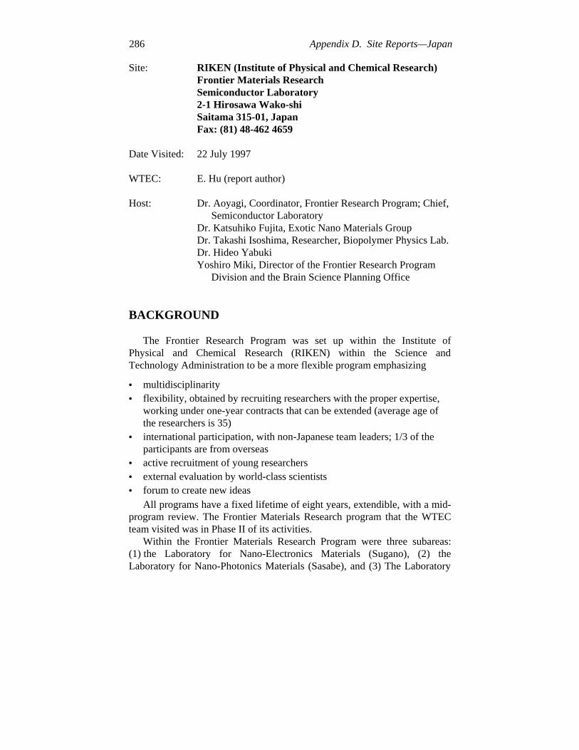
286 Appendix D. Site Reports—Japan
Site: RIKEN (Institute of Physical and Chemical Research)Frontier Materials ResearchSemiconductor Laboratory2-1 Hirosawa Wako-shiSaitama 315-01, JapanFax: (81) 48-462 4659
Date Visited: 22 July 1997
WTEC: E. Hu (report author)
Host: Dr. Aoyagi, Coordinator, Frontier Research Program; Chief,Semiconductor Laboratory
Dr. Katsuhiko Fujita, Exotic Nano Materials GroupDr. Takashi Isoshima, Researcher, Biopolymer Physics Lab.Dr. Hideo YabukiYoshiro Miki, Director of the Frontier Research Program
Division and the Brain Science Planning Office
BACKGROUND
The Frontier Research Program was set up within the Institute ofPhysical and Chemical Research (RIKEN) within the Science andTechnology Administration to be a more flexible program emphasizing
• multidisciplinarity• flexibility, obtained by recruiting researchers with the proper expertise,
working under one-year contracts that can be extended (average age ofthe researchers is 35)
• international participation, with non-Japanese team leaders; 1/3 of theparticipants are from overseas
• active recruitment of young researchers• external evaluation by world-class scientists• forum to create new ideas
All programs have a fixed lifetime of eight years, extendible, with a mid-program review. The Frontier Materials Research program that the WTECteam visited was in Phase II of its activities.
Within the Frontier Materials Research Program were three subareas:(1) the Laboratory for Nano-Electronics Materials (Sugano), (2) theLaboratory for Nano-Photonics Materials (Sasabe), and (3) The Laboratory
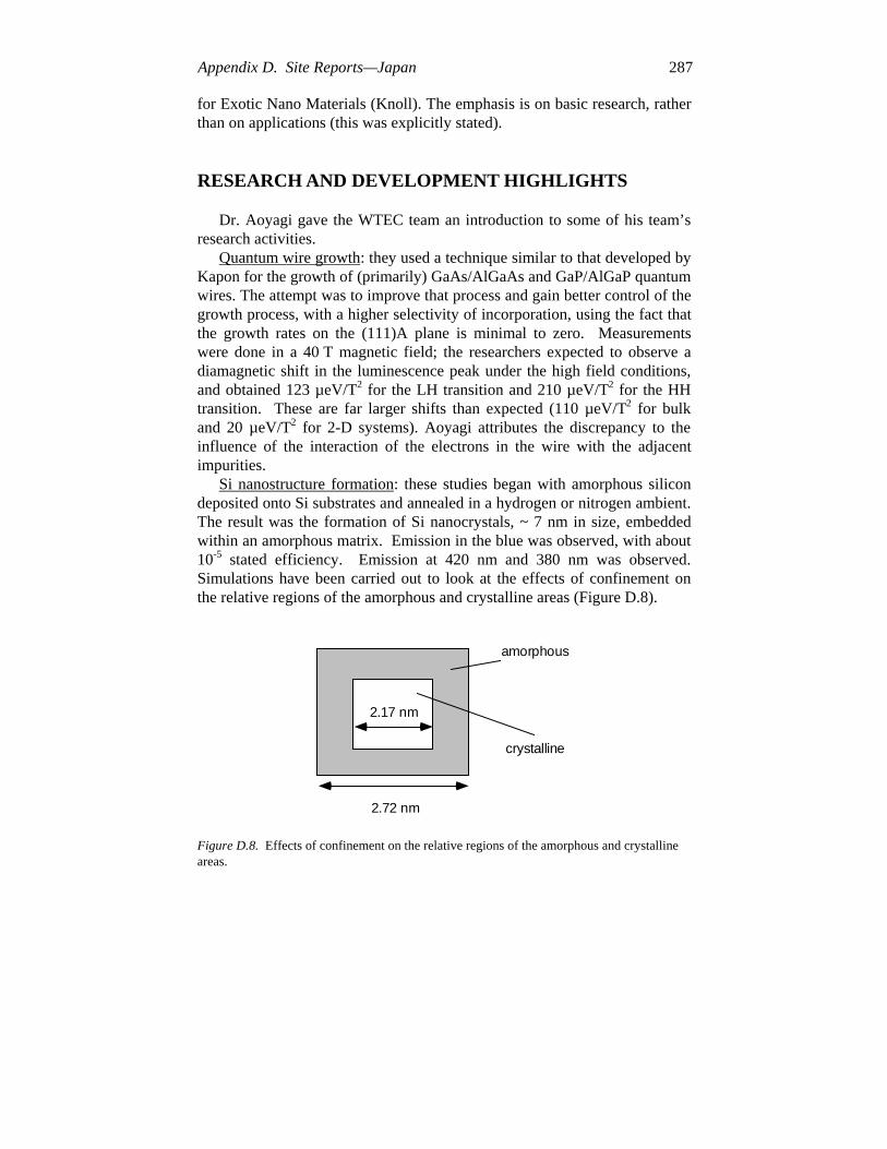
Appendix D. Site Reports—Japan 287
for Exotic Nano Materials (Knoll). The emphasis is on basic research, ratherthan on applications (this was explicitly stated).
RESEARCH AND DEVELOPMENT HIGHLIGHTS
Dr. Aoyagi gave the WTEC team an introduction to some of his team’sresearch activities.
Quantum wire growth: they used a technique similar to that developed byKapon for the growth of (primarily) GaAs/AlGaAs and GaP/AlGaP quantumwires. The attempt was to improve that process and gain better control of thegrowth process, with a higher selectivity of incorporation, using the fact thatthe growth rates on the (111)A plane is minimal to zero. Measurementswere done in a 40 T magnetic field; the researchers expected to observe adiamagnetic shift in the luminescence peak under the high field conditions,and obtained 123 µeV/T2 for the LH transition and 210 µeV/T2 for the HHtransition. These are far larger shifts than expected (110 µeV/T2 for bulkand 20 µeV/T2 for 2-D systems). Aoyagi attributes the discrepancy to theinfluence of the interaction of the electrons in the wire with the adjacentimpurities.
Si nanostructure formation: these studies began with amorphous silicondeposited onto Si substrates and annealed in a hydrogen or nitrogen ambient.The result was the formation of Si nanocrystals, ~ 7 nm in size, embeddedwithin an amorphous matrix. Emission in the blue was observed, with about10-5 stated efficiency. Emission at 420 nm and 380 nm was observed.Simulations have been carried out to look at the effects of confinement onthe relative regions of the amorphous and crystalline areas (Figure D.8).
2.72 nm
2.17 nm
amorphous
crystalline
Figure D.8. Effects of confinement on the relative regions of the amorphous and crystallineareas.
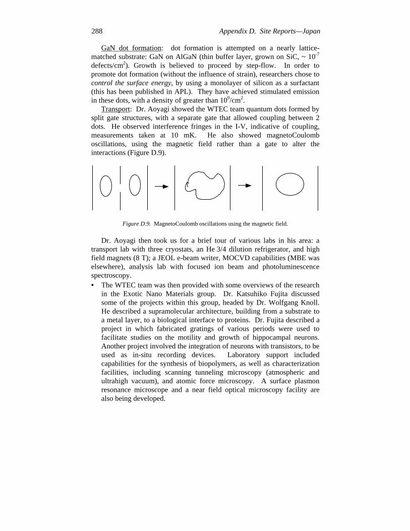
288 Appendix D. Site Reports—Japan
GaN dot formation: dot formation is attempted on a nearly lattice-matched substrate: GaN on AlGaN (thin buffer layer, grown on SiC, ~ 10-7
defects/cm2). Growth is believed to proceed by step-flow. In order topromote dot formation (without the influence of strain), researchers chose tocontrol the surface energy, by using a monolayer of silicon as a surfactant(this has been published in APL). They have achieved stimulated emissionin these dots, with a density of greater than 109/cm2.
Transport: Dr. Aoyagi showed the WTEC team quantum dots formed bysplit gate structures, with a separate gate that allowed coupling between 2dots. He observed interference fringes in the I-V, indicative of coupling,measurements taken at 10 mK. He also showed magnetoCoulomboscillations, using the magnetic field rather than a gate to alter theinteractions (Figure D.9).
Figure D.9. MagnetoCoulomb oscillations using the magnetic field.
Dr. Aoyagi then took us for a brief tour of various labs in his area: atransport lab with three cryostats, an He 3/4 dilution refrigerator, and highfield magnets (8 T); a JEOL e-beam writer, MOCVD capabilities (MBE waselsewhere), analysis lab with focused ion beam and photoluminescencespectroscopy.• The WTEC team was then provided with some overviews of the research
in the Exotic Nano Materials group. Dr. Katsuhiko Fujita discussedsome of the projects within this group, headed by Dr. Wolfgang Knoll.He described a supramolecular architecture, building from a substrate toa metal layer, to a biological interface to proteins. Dr. Fujita described aproject in which fabricated gratings of various periods were used tofacilitate studies on the motility and growth of hippocampal neurons.Another project involved the integration of neurons with transistors, to beused as in-situ recording devices. Laboratory support includedcapabilities for the synthesis of biopolymers, as well as characterizationfacilities, including scanning tunneling microscopy (atmospheric andultrahigh vacuum), and atomic force microscopy. A surface plasmonresonance microscope and a near field optical microscopy facility arealso being developed.
Appendix D. Site Reports—Japan 289
Dr. Takashi Isoshima, a researcher in the Biopolymer Physics Lab(degree from Tokyo University), then described some of the experimentsinvolving polymers for optical devices: ultrafast optical switching, lowpower consumption photorefractives. This group carries out its ownpolymer synthesis, molecular design, and modification, in order to enhanceoptical properties such as nonlinearity and absorption. The goal is tosynthesize multicomponent, photorefractive materials with capabilities inelectrooptic coefficient, photoconductivity, etc. He showed us an impressiveoptical characterization lab: subpicosecond systems, a time-resolvedfluorescence setup (100 fs), three optical benches, and optical fiber devicesfor ultrafast multiplexing.
Dr. Hideo Yabuki then gave us a general overview of RIKEN, its historyand current mission. RIKEN is a semipublic corporation, receiving 95% ofits funding from the Science and Technology Agency. It is believed that thissemipublic status gives it more autonomy. There is extensive collaborationwith universities (University of Tokyo, Tokyo Institute of Technology, andothers), with a number of dual appointments and joint doctoral courses.RIKEN collaborates extensively on an international scale and has establisheda number of laboratories outside of Japan; the Rutherford AppletonLaboratory was the first overseas lab to be established.
Yoshiro Miki, the Director of the Frontier Research Program Divisionand the Brain Science Planning Office (he has been at STA, in MaterialsResearch, and then at MITI on an excimer laser project), spoke of a newpriority project: a brain research institute. Citing a research effort that isonly 10% of that carried out in the United States, promoters of the brainresearch institute hope that this will help to bring “brain science” in Japan upto world-class levels. Miki also spoke of the disconnect between RIKENand the universities in terms of identifying important research priorities;there is a 10-15 years lag between initiation of RIKEN priority programs andobservation of changes in university programs.
EQUIPMENT
Various laboratory equipment included a synthesis lab, with LangmuirTrough, Brewster angle microscope, an analysis laboratory with two STMs,a UHV STM, and AFM. WTEC’s hosts described the development of asurface plasmon resonance microscope (magnification limited), and a nearfield optical microscopy facility that is being built under the coordination ofDr. Ruggiero Micheletto (current resolution is 100 µm).

290 Appendix D. Site Reports—Japan
Site: Tohoku UniversityInstitute for Materials Research (IMR)Katahira 2-1-1, Aoba-kuSendai 980-77, JapanTel: (81) 022-215 2000; Fax: (81) 022-215 2002
Date Visited: 21 July 1997
WTEC: E. Hu, C. Koch, and D. Cox (report authors), L. Jelinski,M. Roco, R.W. Siegel, D. Shaw, C. Uyehara
Hosts: Prof. Kenji Suzuki, Director, Institute for MaterialsResearch; E-mail: [email protected]
Prof. Masayoshi Esashi, Department of Mechatronics &Precision Engineering
Prof. A. Inoue, Head, Nonequilibrium Materials LaboratoryProf. H. FujimoriProf. Kenji SumiyamaDr. Changwu HuDr. Elisabeth KurtzDr. Darren Bagnall
BACKGROUND (Carl Koch)
Most of the WTEC team’s visit to Tohoku University was focused on theInstitute for Materials Research (IMR) which is directed by Professor KenjiSuzuki. IMR’s historical roots go back to 1916; at first it was devoted toresearch on iron and steel. However, under the leadership of ProfessorMatsumoto it became a leading research laboratory in the 1970s and 1980sin the area of nonequilibrium processing techniques for producingmetastable materials, in particular metallic glasses, an area in which it was aworld leader. At present IMR is a large modern materials research centercontaining 26 research laboratories in which approximately 160 scientists,120 technicians, 190 graduate students, and 70 visiting scientists carry out avariety of research projects. The major part of the financial support for theIMR is provided by the Ministry of Education, Science, Sports, and Culture(Monbusho). The specific groups in the IMR concerned with nanoparticles/nanostructured materials that the panel visited are those of Professors K.Suzuki and K. Sumiyama (metallic nanocluster assemblies), ProfessorKasuya (semiconductor nanocluster assemblies), Professor H. Fujimori(magnetic nanostructured materials), Professor A. Inoue (nanostructured
Appendix D. Site Reports—Japan 291
bulk materials), and Professor T. Yao (semiconductor nanodevices). Briefdescriptions of these research efforts are given below. In addition to visitingIMR, the WTEC team visited the Tohoku University laboratory of ProfessorEsashi in the Department of Machine Intelligence and Systems Engineering.Professor Esashi’s research on micro/nano machines is also described.
RESEARCH AND DEVELOPMENT HIGHLIGHTS
Prof. M. Esashi (Lynn Jelinski)
Microsystems by Silicon Machining: This program at TohokuUniversity, under the direction of Prof. M. Esashi, is located on the“mountain” campus of Tohoku, about a 15-minute drive from the maincampus. The program has five components and is staffed by 35professionals. The components are:
• active catheter and piezoelectric films• inertia measurement systems• microactuators and thermal and fluidic micro systems• ultrasensitive sensors and nanostructures• semiconductor research institute
The professionals comprised postdoctoral fellows from a number ofcountries, resident staff, and employees of a number of companies, includingSamsung, Ford, Hitachi, Asahi Optical, and Honda.
Prof. Esashi has been working in the area of microelectromechanicalsystems (MEMS) devices for the past 25 years and over that time built up afairly sophisticated, albeit homemade, facility for producing MEMS devicesand another facility for characterizing them. A number of biomedicaldevices have been produced over the years, including blood gas sensors, a1 mm diameter, navigable catheter based on shape-memory alloy material,produced with an STM tip, using a heated silicon substrate.
In the past several years there have been major capital investments intothe program, resulting in the building and equipping of a microfabricationfacility and a separate nanofabrication facility.
The microfabrication facility, also called a Venture Business Laboratory,was constructed and outfitted with government money. Companies areencouraged to make use of the facilities. The names of 27 companies, mostof them large and well known, were displayed in the entryway.
The microfabrication facility consisted of a 0.5 micron CMOS line for2-inch wafers, and housed an impressive array of modern equipment,including He-Cd and Ar lasers for laser fabrication, and laser-induced CVD.
292 Appendix D. Site Reports—Japan
This facility was very heavily invested in etch equipment, which included amolecular beam etch station for fairly sophisticated controlled etching.There was room after room of characterization equipment, including fieldemission SEM, SIMS, an SEM for characterizing biological systems underwater, and an in situ monitor. There was also highly specialized equipment,including an entire room devoted to sensor characterization, which housedan accelerometer tester that worked in vacuum and a position-sensitivedevice that also worked in vacuum.
The nanofabrication facility, a Class-1000 cleanroom, was about a yearold. Like the microfabrication facility, it was equipped with an impressivearray of new and sophisticated equipment, including an e-beam directexposure system and a stepper/pattern generator. It is conservativelyestimated that the facility cost $10 million.
There was also a nanodevice characterization room, including ultrahighvacuum AFM, STM, STEM, and ESCA. An in situ infrared ellipsometerwas available for characterization of epitaxial layers.
While the size scale of the micro- and nanomachines we learned aboutwere larger than that covered in this report, two projects bear description:1. Esashi and coworkers (Ono et al. 1997) described the use of an ultrahigh
vacuum STM to produce a silicon nanowire via field evaporation ofsilicon. A gold STM tip was positioned over a clean silicon substrate, thelater of which was held at 700°C. At an applied sample voltage of 5 V(10 nA tunneling current) for 15 min., with the tip positioned 6 Å abovethe surface, growth of the silicon nanowire could be monitored by in situSEM. The diameter ranged between 20-150 nm and the length was about3 mm. Electron diffraction patterns showed that the wire was silicon,with between 2 and 15 at.% gold on its surface. It is posited that the fieldevaporation of silicon is enhanced by the formation of an Au-Si eutecticon the substrate.
2. In other work, the group described a self-supported silicon nanostructurethat had been fabricated on a silicon diaphragm (Hamanaka et al. 1997).
Prof. H. Fujimori (Carl Koch)
The focus of Professor Fujimori’s group is on new developments in thefield of magnetic materials. A major part of this effort is directed atnanocrystalline (nc) Fe-based soft magnetic materials. A major method ofprocessing utilizes preparation of amorphous precursors by melt spinning orsputtering followed by partial crystallization of nc bcc Fe particles. The ncFe particles provide high magnetic moments and, if < about 20 nm indiameter, exhibit small crystalline anisotropy and superior soft ferromagneticproperties. An example given is an Fe-base amorphous alloy produced by

Appendix D. Site Reports—Japan 293
sputtering that contains Hf, Ta, C, which on crystallization gives 10 nm Feparticles whose grain boundaries are pinned by about 10 nm diametercarbide (e.g., Fe80Hf8C12) particles, which stabilize the nm grain size up toelevated temperatures (~ 700°C). This material exhibits almost constantpermeability µ', with frequency up to about 10 MHz while the µ"(imaginary, lossy) component rises at values between 1 and 10 MHz.
Another interesting topic involves preparation and propertymeasurements of metal/nonmetal granular nc composites. Sputtering wasused to form systems such as Fe/SiO2, Co/Al2O3. As the oxygenconcentration in the films increases, the electrical resistivity increases frommetallic (101–102 µΩcm), to a ρ vs. T behavior with a ρ minimum withρ = 102–103 µΩcm, to high resistivity (negative coefficient of ρ) withρ = 104–1010 µΩcm. The low oxygen content composites showferromagnetic behavior with high permeabilities—about double that offerrites but with higher losses. A potential application is use as a highfrequency inductor.
The oxygen-rich composites exhibit giant magnetoresistance (GMR). Forexample, the Co, Fe in Al2O3 provides an assembly of tiny tunnelingjunctions with ∆ρ/ρo about 7.8%.
Fujimori’s magnetic materials program is expected to receive anadditional $3.8 million in government funding for the next five years in anew program entitled, “Nanostructurally controlled spin dependent quantumeffects and new electronics and magnetics.” A goal is a one-electron spinmemory.
Prof. A. Inoue (Carl Koch)
Professor Inoue’s large group (41 persons) studies amorphous, quasi-crystalline, and nc materials. The nc materials are typically prepared bycrystallization of amorphous precursors, which can be bulk amorphousalloys, ribbons or wires produced by melt spinning, or rapidly quenchedpowders produced by powder atomization methods. Mechanical tests onnc/amorphous alloys from bulk amorphous samples exhibit increased yieldstrengths but little elongation in tension—that is, behavior similar toamorphous alloys even though 60–70 vol.% of the material is crystalline.Mg-base alloys have been successfully studied in this regard.
The equipment for processing, material characterization, and propertymeasurements in Inoue’s laboratory is very impressive indeed, with mostnonequilibrium processing tools, sophisticated characterization, and propertymeasurement facilities available.
The innovative work on metastable materials Professor Inoue has carriedon over the years cannot be praised too highly. He and his coworkers are
294 Appendix D. Site Reports—Japan
responsible for a new class of soft ferromagnetic materials based on Fe-Zr-Bcompositions that consist of nanocrystalline bcc Fe particles in anamorphous matrix. These materials exhibit the lowest core losses atfrequencies up to 400 Hz of any known material. They have also developedalloys based on Al or Mg, which are two-phase nanocrystalline andamorphous and which exhibit high strength, e.g., the Al alloys have morethan double the strength of the strongest existing Al alloys, along with someductility.
A major factor in his group is its close association with Japaneseindustry. This is illustrated by the fact that 20 of his 41-member group areemployees of many companies, specially assigned to carry out research inhis group.
Profs. K. Suzuki and K. Sumiyama (Don Cox)
Prof. Kenji Sumiyama and Dr. Changwu Hu gave highlights of some ofthe work being done in the areas of metallic nanocluster assemblies andwork on fullerenes and carbon nanotubes, respectively. In the metallicnanocluster area the main focus is on developing different techniques forproduction of metallic clusters.
Prof. Sumiyama described five different techniques for production ofmetallic clusters that have been utilized by his group:1. ionized cluster beam deposition2. plasma sputtering with cluster aggregation3. field emission of atoms from a metal (gold) tip4. liquid metal ion source5. laser ablation cluster source
For characterization their main tools are electron microscopes, e.g., SEM,FE-TEM, and STM examinations of clusters deposited on substrates. Theprimary use appears to be for evaluation of the cluster size and cluster sizedistribution from the various cluster production techniques. Everyresearcher appears to be well equipped, with each possessing electronmicroscopes for individual use. They reported plans to add electronholography capability to the field-emission TEM next year. In addition touse as cluster size and size distribution measurements, recent STM studies ofselenium clusters deposited on HOPG were interpreted as the first evidencefor six or eight metal atom rings covering an HOPG surface.
The ionized cluster beam apparatus is the most developed and was anearly workhorse, with several publications reporting work using this source.More recently, a new plasma sputtering apparatus has been constructed overthe last four years and has become the primary cluster synthesis apparatus atIMR. Drs. Suzuki and Sumiyama reported being able to produce clusters of
Appendix D. Site Reports—Japan 295
smaller sizes and with narrower size distributions than was possible with theionized cluster beam apparatus and are optimistic that this source can bescaled up for much larger production than currently feasible. For example,with the plasma sputtering apparatus, they reported production of chromiumclusters with sizes ranging between 3-4 nm with about 10% variation in size.Previously, the average cluster size was about 8-9 nm, but with a largervariation in size. Optimization of the helium and argon gas mixtures used inthe plasma sputtering have resulted in better control of the cluster size andcluster size distribution, according to Prof. Sumiyama. The laser ablationcluster source is now being developed for production of transition metalclusters. The other two techniques, field emission and liquid metal ionsource, are not as versatile, being limited to materials that have relativelylow melting points.
Dr. Changwu Hu (Don Cox)
Dr. Hu described the efforts at Tohoku in the area of fullerene and carbonnanotube production and characterization. Dr. Hu described three mainitems:1. chemical reaction studies of C60 on Si(111)2. polymerization of C60 and C84 by argon ion laser irradiation3. production and characterization of single-walled carbon nanotubes
In (1), the chemical reaction of C60 on Si(111), C60 is deposited onSilicon(111) and then heated to 800°C. At 800°C STM shows that amonolayer of C60 in registry with the Si(111) surface is covering the surface.Upon further heating to 850°C, the C60 layer becomes disordered. Heatingeven further to 1100°C results in formation of SiC in the form of SiCclusters of about 50 nm diameter and 2-4 nm height. This technique isreported to be a novel low temperature route to SiC.
In (2) the fullerenes are observed by STM to polymerize upon irradiationby an Ar ion laser and form large (150 nm diameter) clusters. Additionalstudies showed that the STM pattern changed with changing bias voltage,suggesting some polymerization is induced by the STM electric fields.
Lastly, Dr. Hu reported recent results on characterization of nanotubesproduced in the laboratory. The researchers report single-walled nanotubeyields of 20-30%, and that the diameter of the single-walled nanotubedepends on the metal used in their (metal catalyzed) production, e.g.,nanotube radii of 0.5 nm, 0.65 nm, and 1.0 nm for Fe/Ni, Co, and La,respectively. Raman spectroscopy and STM are used to characterize thenanotube deposits. Attempts to interrogate the electronic structure have beenunsuccessful thus far.
296 Appendix D. Site Reports—Japan
The overall picture is that this group at Tohoku is well equipped as far asthe electron microscopy techniques are concerned and is primarily interestedin developing larger scale production techniques for both metallic clustersand for carbon nanotubules. It was not clear what the ties to futuretechnology development may be.
Prof. T. Yao’s Lab: Drs. D. Bagnall and E. Kurtz (Evelyn Hu)
Dr. Takafumi Yao’s general research goal is “to exploit newoptoelectronic materials for the 21st century.” The WTEC team’s visit toProfessor Yao’s laboratories was hosted by two postdocs working with him:Dr. Elisabeth Kurtz and Dr. Darren Bagnall. Drs. Kurtz and Bagnall are twoof three foreign (JSPS) postdocs working within Dr. Yao’s lab. (Thislaboratory is apparently one of three under Professor Yao’s supervision;another one is located in Tsukuba). They described projects in thenanostructured growth of wide bandgap materials: ZnO and CdSe.
Dr. Bagnall spoke of Plasma-Assisted MBE of ZnO for Blue-UVEmitters. A plasma source of oxygen was used to assist the epitaxial growthof ZnO on sapphire substrates. Free exciton emission dominates at roomtemperature, and pulsed, optically-excited lasing was observed up to 500 K,with fairly large thresholds: 2.5 MW/cm2. With the large amount of strainbetween ZnO and sapphire, it would not be surprising to observenanostructure growth (e.g., islands). In fact, AFM traces showed evidenceof pyramidal structure: this was not thought to be the basis of the excitonicemission. Bagnall hopes to grow quantum wells in this material structure.
Dr. Kurtz described the growth of self-organized quantum dots in theCdSe material system: (111)A ZnSe was grown on a GaAs substrate, andCdSe dot structures were subsequently nucleated on this surface. The(111)A surface was utilized because it provided a smooth, featurelesssurface. The dots had typical diameters of 47 nm, with a height/diameterratio of 19%. There are some interesting differences in these dots comparedto self-organized dots in the III-V materials, such as InAs/GaAs:
• They have less stability: the dot dimensions are not stable with time, dueto Ostwald ripening.
• Under different growth conditions, the dot sizes do not change, althoughthe densities do change. Typical densities range from 5-25(µm)-2 (usingatomic layer epitaxy with either 1 or 3 cycles of growth). In the III-Vmaterials, the dot diameter and dot density are usually coupled, i.e., onecannot change one parameter without having the other parameter alsovary.
Appendix D. Site Reports—Japan 297
Both projects used cathodoluminescence, photoluminescence, and AFMmeasurements in their analysis. There was a lack of modeling effortcomplementing the experimental work of the group. There seemed to beaccess to a broad range of characterization tools within or external to theYao group—such as near field scanning optical microscopy. The WTECteam was taken for tours of some of the Yao labs, which include five MBEstations, cathodoluminescence (CL), photoluminescence (PL), X-rayanalysis, and a UHV STM.
REFERENCES
Ono, T., H. Saitoh, and M. Esashi. 1997. Si nanowire. In growth with ultrahigh vacuumscanning tunneling microscopy. Applied Physics Letters 70(14)(7 April).
Hamanaka, H., T. Ono, and M. Esashi. 1997. Fabrication of self-supported Si nano-structurewith STM. In Proc. of IEEE, MEMS ‘97 (January), pp. 153-158.
298 Appendix D. Site Reports—Japan
Site: Tokyo Institute of TechnologyNagatsuta, Midori-kuYokohama 226, JapanTel: (81) 45-924 5759; Fax: (81) 45-924 5779
Date Visited: 21 July 1997
WTEC: L. Jelinski (report author), E. Hu, M.C. Roco, D. Shaw,C. Uyehara
Host: Professor Masuo Aizawa, Faculty of Bioscience andBiotechnology; E-mail: [email protected]
BACKGROUND
The Tokyo Institute of Technology has two campuses, one at Tamachiand another at Nagatsuta. The Nagatsuta Campus is about 20 years old, andthe Faculty of Bioscience and Biotechnology was moved there about sixyears ago.
RESEARCH AND DEVELOPMENT HIGHLIGHTS
Professor Aizawa, whose laboratory the WTEC team visited at the TokyoInstitute of Technology’s Nagatsuta Campus, was the project leader of a ten-year national MITI project on bioelectronic devices. The project, whichended in 1995, involved eight electronics companies and two national labsfor its initial five-year period. One of the electronics companies dropped outand did not participate in the second term. An example of the workperformed in the project is that by Mitsubishi, which produced an artificialprotein that binds an electron acceptor and electron donor.
It appears that much of what was accomplished in the MITIbioelectronics project was accomplished in Aizawa’s laboratory (see below).He set out to answer the question, “Are biological systems ideal formolecular electronics or not?” Parts of the project that are being continuedappear to be in the form of RIKEN’s Brain Research Center. Formulation ofideas for somewhat related work is being carried out by the IntelligentMaterials Forum, whose members are working to promote a national projectin this area. (The president of the forum is Toshinori Takagi; Aizawa is thevice president.) The idea of intelligent materials is to incorporate sensingand transduction and information processing into the same materials. The
Appendix D. Site Reports—Japan 299
idea of forming a “Nanospace Laboratory” was just coming together at thetime of the WTEC visit.
Aizawa has been a world leader in bioelectronics. His review onmolecular interfacing for protein molecular devices and neurodevices(Aizawa 1994) describes subjects such as the coupling of electron transferproteins (e.g., glucose oxidase) to solid surfaces, conducting polymer wiresthat couple the enzyme to the surface, and electrically modulated activity ofmolecular-interfaced enzymes.
More recent work, not yet published at the time of the WTEC visit,involved developing methodology to orient antibodies on surfaces. The keyto making this work was to genetically modify protein A, known to bind thenon-antigen binding stalk of the “Y” of the antibody, so its C-terminalcarried a cysteine. The modified protein A was then bound to a gold surfacevia the well-known alkylthiol/gold chemistry. The ability to control theorientation of proteins on the surface is a major step forward in the ability touse these systems for drug targets, biochemical purifications and separations,and for sensing and diagnostic applications.
In other experiments, liposome nanoparticles were engineered bycoupling to phosphatidyl choline, a peptide corresponding to one antigenbinding domain of an antibody (Kobatake et al. 1997). These nanoparticleswere used as the basis for a new fluoroimmunoassay.
REFERENCES
Aizawa, M. 1994. Molecular interfacing for protein molecular devices and neurodevices.IEEE Engineering in Medicine and Biology (February/March).
Kobatake, E., H. Sasakura, T. Haruyama, M.-L. Laukkanen, K. Keinänen, and M. Aizawa.1997. A fluoroimmunoassay based on immunoliposomes containing geneticallyengineered lipid-tagged antibody. Analytical Chemistry 69(7): 1295-1298.
300 Appendix D. Site Reports—Japan
Site: The University of TokyoDepartment of Chemical EngineeringFaculty of EngineeringKogakukan #5, Room 709Bunkyo-ku, Tokyo 113, JapanFax: (81) 3-5689 7352
Date Visited: 22 July 1997
WTEC: D.T. Shaw (report author)
Hosts: Prof. H. Komiyama, Dept. of Chemical Systems EngineeringDr. H.S. ZhouDr. Fumihiro Wakai, Professor, Center of Materials Design,
Tokyo Institute of Technology, Yokohama
BACKGROUND
The University of Tokyo is the oldest and the most prestigious universityin Japan. Prof. Komiyama belongs to the Department of Chemical SystemsEngineering, which is one of three departments (the other two are theDepartment of Applied Chemistry and the Department of Chemistry andBiotechnology) in the Department of Chemical Engineering. His work onnanoparticles has focused on the synthesis and optical properties ofnanocomposites of metal/organic, organic/metal, metal/semiconductor, andsemiconductor/semiconductor particles. More recently, coated self-assembled nanoparticles have also been studied.
Overall, Prof. Komiyama’s work on nanoparticles and nanoparticlestructures has focused on fundamental studies of the effects of quantumconfinement of heterostructured nanoparticles and nanoparticle structures.Prof. Komiyama’s laboratory is extremely well equipped and has formedstrong connections to other research laboratories both within and outsideJapan. At the present time, all his research projects appear to beexperimental. In fact, the last theoretical work was conducted in cooperationwith Prof. Joseph W. Haus (Physics Department, Rensselaer PolytechnicInstitute, RPI) who visited him for one year in 1992.
Appendix D. Site Reports—Japan 301
RESEARCH AND DEVELOPMENT HIGHLIGHTS
Dr. H.S. Zhou, who is now a researcher at the ElectrotechnicalLaboratory at Tsukuba City, showed me his work with Prof. Komiyama onthe study of conformational change of protein cytochrome b-562 absorbedon colloidal gold particles. Cytochrome b-562 is a small cylindrical haemprotein (diameter ~2.5 nm and height ~5 nm) found in the periplasm of E-coli. Depending on the degree of coverage, the protein on the gold particles(diameter ~ 31 nm) can be in side-on or tail-on conformation. Maximumoptical shift occurs when protein particles are in side-on conformation withan effective composite particle size of 36 nm. Other work in this areaincludes the synthesis of semiconductor/semiconductor (such as CdS/PbS)and metal-coated (such as AuS/Au, Ag/polydiacetylene) particles. Some ofthis work was partially inspired by the theoretical work carried out whileProf. Haus was visiting Tokyo University on leave from RPI in 1992. Inrecent years, special emphasis has been placed on experimental projectsbecause of the great influx of equipment funds from the government. Atpresent, nanoparticles are fabricated by colloidal chemical vapor depositionand physical vapor deposition techniques (e.g., laser ablation, sputtering, andelectron cyclotron resonance).
Dr. Fumihiro Wakai was invited by Prof. Komiyama to make apresentation on his work on superplasticity. Dr. Wakai was associated withthe National Industrial Research Institute of Nagoya. He is now a professorat the Center of Materials Design at the Tokyo Institute of Technology inYokohama. His work (Nature 1990. 344:421) on Si3N4/SiC composites hasled to the discovery of superplasticity in nanocrystalline covalent ceramicmaterials. Currently, he is also the director of a large cooperative projectbetween Japan and Germany (Prof. Fritz Aldinger, Max-Planck-Institut fürMetallforschung), supported by the Japan Science and TechnologyCorporation, that commenced its operation in October 1966. The objectivesof the cooperative project are to explore the nanostructures of thesuperplastic grain boundaries and to develop new synthesis techniques formaximum superplastic deformation at elevated temperatures. In addition,Prof. Komiyama mentioned the possibility of investigating theminiaturization of superplastic testing and characterization with a very smallamount of materials.
CONCLUDING REMARKS
Although I spent all of my visit with Prof. Komiyama’s group, there areseveral other groups at the University of Tokyo that are conducting
302 Appendix D. Site Reports—Japan
significant research in nanotechnology. These include the PhysicsDepartment (theoretical and experimental work on quantum-confinementand functional materials) and the Department of Applied Chemistry (TiO2
particles).Although my two-hour visit concentrated on composite
nanoparticles/nanostructures as described above, I know from my previousvisit in October 1996 that Prof. Komiyama is also active in areas related toamorphous silicon and other metal and semiconductor nanostructuredmaterials. He is one of the research leaders in the one-step CVD synthesis ofAlN, TiN, SiN, SiC, TiC, and ZrO (single or two components)nanostructured materials.
Appendix D. Site Reports—Japan 303
Site: Toshiba Research and Development Center1 Komukai, Toshiba-choSaiwai-ku, Kawasaki 210, JapanTel: (81) 44-549 2318; Fax: (81) 44-520 1287
Date Visited: 24 July 1997
WTEC: H. Goronkin (report author), E. Hu, L. Jelinski, M.C. Roco,D. Shaw, C. Uyehara
Hosts: Mr. Haruo Nakatsuka, R&D CenterDr. Koichiro Inomata, R&D CenterDr. Masaaki Tamatani, Materials and Devices Research LabsDr. Shuji Hayase, Materials and Devices Research LabsDr. Takashi Kawakubo, Materials and Devices Research LabsDr. Atsushi Kurobe, Advanced Research LaboratoryMr. Kunio Yoshihara, Advanced Semiconductor Devices
Research Laboratories
BACKGROUND
Toshiba has a history over 100 years. In 1939, Shibaura EngineeringWorks and Tokyo Electric Company were merged to a single companynamed Tokyo Shibaura Electric Company. In 1978, it changed its named toToshiba Corporation.
Toshiba has a 3-layered R&D organization with long-, medium- andshort-term elements: the corporate laboratories work on new technology thatmay be applied to products 5 to 10 years later; the development laboratoriesare working on technology for deployment 3 to 5 years later; the engineeringdepartments in the operating divisions have as their most important task thesolution of problems inherent to present products.
RESEARCH AND TECHNICAL HIGHLIGHTS
The following sections summarize the ongoing work in various Toshibalaboratories concerned with nanostructure technologies, based onpresentations made to the WTEC panel by our hosts.
304 Appendix D. Site Reports—Japan
A. Kurobe, Advanced Research Laboratory
“Study of Shapes Produced by Stranski-Krastanov Growth in Cold-WalledUHV-CVD”
With a silicon buffer, hut-shaped Ge dots with (001 x 010) alignmentwere obtained. Without a buffer, dome-shaped Ge dots were obtained.Using H-terminated Si wafers by exposure of atomic hydrogen, domes wereobtained.
The H-free wafers with a prior annealing at 750oC contained the hut dots.Thermal desorption spectroscopy supports the difference in the surface:Dihydride desorbs at 415oC. Monohydride desorbs at 550oC. Annealing at750oC removes all H. Atomic hydrogen exposure produces a monohydridesurface. The goal is study of interaction of dots with 2DEG. The plan is tomove to a SiO2-Si system to increase barrier height.
K. Inomata, Research and Development Center
“Advanced GMR”Working on spin electronics for high density heads, 20 Gbit in 2002 is
forecast. Toshiba researchers have achieved >10% GMR ratio in layeredfilms at room temperature. They have also achieved > 30% in nanogranularfilms with a coercive field of 0.1 T.
The most promising approach is the tunnel junction. It has > 25% MRratio but drawbacks include high resistance and strong fall-off of themagnetoresistance ratio with applied voltage and pinholes in the ultrathininsulator barrier.
Dr. Inomata described two structures for possible use in future memoryand logic. One new proposed structure consists of two ferromagnetic (FM)layers sandwiching a barrier containing 8 nm granules of FM material in anSiO2 matrix. The total barrier thickness is about 10 nm. Inomata andcoworkers explained that the size and distribution of the FM granules mustbe carefully controlled. The FM contact polarization can be switched eitherparallel or antiparallel to the granules and to each other to provide high orlow current transport through the barrier. No data were provided.
A second proposed structure places the two FM electrodes on the samesurface of granular FM materials. This is a transistor structure in whichlateral conduction can be controlled by the relative polarization of thecontacts. No data were provided.
Appendix D. Site Reports—Japan 305
T. Kawakubo, Materials and Devices Research Laboratories
“Epitaxy of Ferroelectric (FE) Materials”The goal of this project is to control FE properties by orientation and
strain of the epitaxial material.The researchers use (Sr, Ba)TiO3 with SrRuO3 electrodes, which have
good metallic conduction. By reducing the thickness and sputter conditions,good performance (saturating hysteresis loop) at 1.0 V has been obtained.This material is also under investigation for DRAM charge storagecapacitors. With 20% Ba content, the dielectric constant is about 900. AnSiO2 equivalent thickness of 0.085 nm was obtained. The leakage currentwas 4 x 10⁻⁸ A/cm2 between ±1.3 V. This was said to be satisfactory for0.12 µm DRAM. TiAlN/Pt barrier layers were used.
M. Tamatani, Materials and Devices Research Laboratories
“Nanoparticle Phosphors Made by Thermal Plasma”This project produces spherical particles compared to faceted particles.
These particles have the particle size in the same region as those ofcommercially available materials. They must be heat treated in oxygen orhydrogen to restore luminescence efficiency comparable to that of thecommercial phosphors. The thermal plasma also produces nanoparticlephosphors, which could be used as labeling agents for analysis.
306 Appendix D. Site Reports—Japan
Site: ULVAC Japan, Ltd.Vacuum Metallurgical Company (VMC)516 Yokota, Sanbu-cho, Sanbu-gunChiba 289-12, JapanFax: (81) 467-87 3383
Date Visited: 23 July 1997
WTEC: D. Shaw (report author), C. Koch, R.W. Siegel, C. Uyehara
Hosts: Dr. Chikara HayashiDr. Masaaki Oda
BACKGROUND
The Vacuum Metallurgical Company (VMC) is a subsidiary of ULVACJapan, Ltd., which is a relatively large conglomerate of 30 companiesemploying over 3,500 people. The principal products of VMC includesputtering targets; complex shaped Ti-alloy cast parts; reactive andrefractory metal sheet, wire, and shapes; and service coating for processingequipment for semiconductors, display panels, etc.
VMC’s ultrafine-particle (UFP) business is based on early work by Dr.Hayashi and colleagues on gas-phase particle nucleation (evaporation andcondensation) and deposition by using nanoparticles dispersed in tiny gasjets (in the 10 micron diameter range). VMC commercialized magnetic UFPin 1971, and Dr. Hayashi (at the time, president of ULVAC) served as theleader of a UFP project in Japan’s Exploratory Research in AdvancedTechnology (ERATO) program from 1981-1986. ERATO has beensupported by the now renamed government organization, Japan Science andTechnology Corporation (JST). The UFP project investigated the physical,chemical, and biological properties of nanoparticles.
Over the years, VMC has improved the magnetic UFP technique and nowoffers a large quantity of metallic and organic particles; gas-evaporation andgas-deposition equipment for producing fine pattern of contacts andconductive lines for electronic devices; and UFP paste (dispersed liquid)with coating system.
RESEARCH AND DEVELOPMENT HIGHLIGHTS
Although the basic design of the induction-heating chamber for theultrafine-particle generation was developed by Hayashi and Oda in the
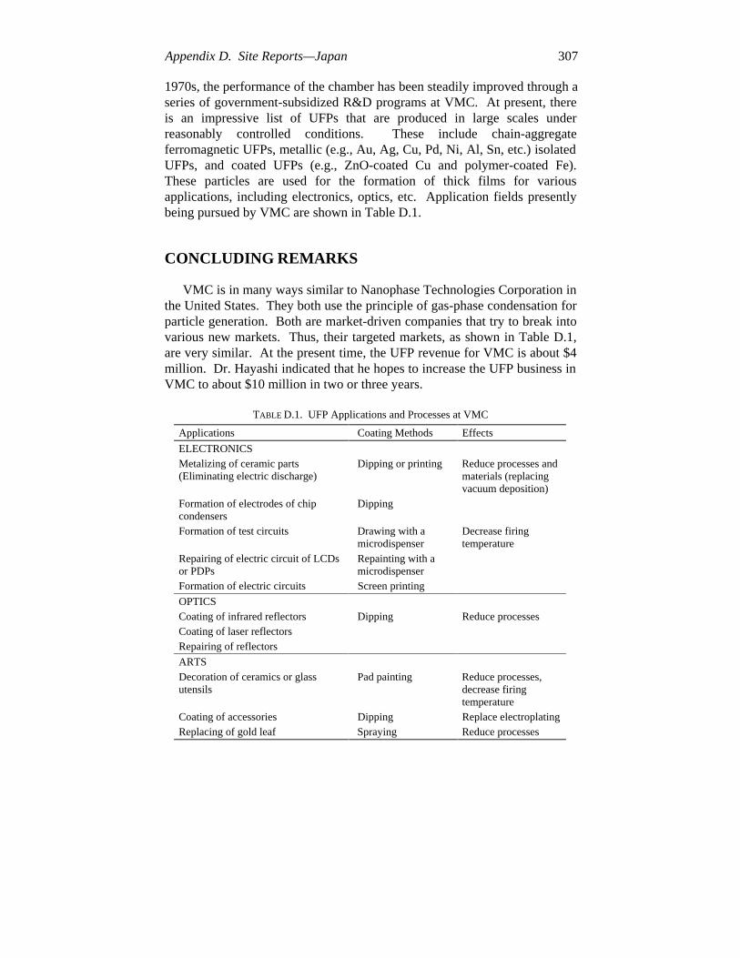
Appendix D. Site Reports—Japan 307
1970s, the performance of the chamber has been steadily improved through aseries of government-subsidized R&D programs at VMC. At present, thereis an impressive list of UFPs that are produced in large scales underreasonably controlled conditions. These include chain-aggregateferromagnetic UFPs, metallic (e.g., Au, Ag, Cu, Pd, Ni, Al, Sn, etc.) isolatedUFPs, and coated UFPs (e.g., ZnO-coated Cu and polymer-coated Fe).These particles are used for the formation of thick films for variousapplications, including electronics, optics, etc. Application fields presentlybeing pursued by VMC are shown in Table D.1.
CONCLUDING REMARKS
VMC is in many ways similar to Nanophase Technologies Corporation inthe United States. They both use the principle of gas-phase condensation forparticle generation. Both are market-driven companies that try to break intovarious new markets. Thus, their targeted markets, as shown in Table D.1,are very similar. At the present time, the UFP revenue for VMC is about $4million. Dr. Hayashi indicated that he hopes to increase the UFP business inVMC to about $10 million in two or three years.
TABLE D.1. UFP Applications and Processes at VMC
Applications Coating Methods Effects
ELECTRONICSMetalizing of ceramic parts(Eliminating electric discharge)
Dipping or printing Reduce processes andmaterials (replacingvacuum deposition)
Formation of electrodes of chipcondensers
Dipping
Formation of test circuits Drawing with amicrodispenser
Decrease firingtemperature
Repairing of electric circuit of LCDsor PDPs
Repainting with amicrodispenser
Formation of electric circuits Screen printing
OPTICSCoating of infrared reflectors Dipping Reduce processesCoating of laser reflectorsRepairing of reflectors
ARTSDecoration of ceramics or glassutensils
Pad painting Reduce processes,decrease firingtemperature
Coating of accessories Dipping Replace electroplatingReplacing of gold leaf Spraying Reduce processes
308 Appendix D. Site Reports—Japan
NOTES ON FUNDING OF NANOTECHNOLOGYRESEARCH IN JAPAN
M.C. Roco
Introduction
Government organizations and very large corporations are the mainsource of funding for nanotechnology research and development in Japan.Small and medium-size companies play a minor role. All large Japanesecorporations devote a significant portion (generally ~ 10% in the electronicsindustry) of their income to R&D. Japanese corporate research tends to beproduct-oriented, but there is also a well-established culture within thecorporate and scientific community of planning for the next generation oftechnological innovation. As evident in the foregoing site reports,nanotechnology R&D is decidedly a part of the present and future planningof both government and industry labs, and funds are allocated accordingly.
Government funding for nanotechnology research should be viewed inthe context of the overall increase of public support for basic research since1995 as a result of passage of Japan’s Science and Technology Basic LawNo. 130 (effective November 15, 1995). The law proposes to allocateapproximately ¥17 trillion (~$148 billion1) for basic research to Japaneseuniversities, industry, and national laboratories from 1996 to 2000. Themain recipients of the 1996 government budget for science and technology($23.3 billion/year) were the Ministry of Education, Science, Sports, andCulture (known as Monbusho), which received 46.5% of the S&T budget;the Science and Technology Agency (STA), which received 25.9%; and theMinistry of International Trade and Industry (MITI), which received 11.9%.In 1997 the university system received $935 million from Monbusho as“grants-in-aid” for research, and $239 million from other ministries,however, it appears that the ministry with the largest allocation of fundsspecifically earmarked for nanotechnology R&D is MITI.
The information on funding presented here is based on interviews withJapanese colleagues during the WTEC panel’s visit in July 1997, using thenanotechnology definition adopted by this study. All budgets are for thefiscal year 1996 (April 1, 1996 to March 31, 1997) and are approximate. Inmany institutions it was difficult to separate the exact contribution ofresearch related to nanostructure science and technology, and for thoseinstitutions, only the total budget, as available, is given.
1 The exchange rate used throughout this overview is ¥115 = $1, unless otherwise stated; thebudgets given are for FY 1996.
Appendix D. Site Reports—Japan 309
A. Main Japanese Government Organizations SponsoringNanotechnology R&D
MITI / AIST (Agency of Industrial Science and Technology)
Total budget, $2.75 billion/year; nanotechnology budget from all sourcesbelow, ~$60 million/year
National Institute for Advancement of Interdisciplinary Research (NAIR),Tsukuba City• Joint Research Center for Atom Technology (JRCAT), ten-year budget of
~$220 million (1992-2001); $25 million/year• Research on Cluster Science, ~$10 million (1992-1997); $2 million/year• Research on Bionic Design, ~$10 million (1992-1997), 50% for
nanotechnology; $1 million/year
Electrotechnical Laboratory, Tsukuba City• Total budget, ~$100 million/year; nanotechnology budget, ~$17 million
Osaka National Research Institute, Osaka• Total budget, ~$26 million/year; estimated nanotechnology budget,
~$3 million/year
National Industrial Research Institute of Nagoya (NIRIN), Nagoya• Total budget, ~$25.2 million/year (1996); estimated nanotechnology
budget, ~$2.5 million/year
MITI’s Quantum Functional Devices (QFD) Program• Ten-year budget ~$64 million (1991-2001); estimated nanotechnology
budget, ~$6.4 million/year
Science and Technology Agency (STA)
Total budget, $6 billion/year; estimated nanotechnology portion was~ $35 million/year in FY 1996
Institute of Physical and Chemical Research (RIKEN), Wako City• Total budget, $300 million/year; nanotechnology budget is included in
Frontier Materials research
National Research Institute for Metals (NRIM), Tsukuba City• Total budget, $130 million/year; nanotechnology work in various projects
National Institute for Research in Inorganic Materials (NIRIM), Tsukuba City• Total budget, $35 million/year; nanotechnology budget, ~$0.8 million
310 Appendix D. Site Reports—Japan
Japan Science and Technology Corporation (JST)• Administration of ERATO Program (Exploratory Research for Advanced
Technology), including 4 nanotechnology projects, each with totalbudgets of $13-18 million for five years:– Quantum Wave Project (1988-1993)– Atomcraft Project (1989-1994)– Electron Wavefront Project (1989-1994)– Quantum Fluctuation Project (1993-1998)
Ministry of Science, Education, Sports, and Culture (Monbusho)
Total budget, $10.8 billion/year
Nanotechnology programs are supported at universities and nationalinstitutes, as well as via the Japan Society for Promotion of Science (totalresource allocation unknown).
Tokyo University, Tokyo• University of Tokyo’s Research Center for Advanced Science and
Technology• Institute of Industrial Engineering• Chemical Engineering (H. Komiyama) (A newsletter “Quantech” for a
loose network on nanotechnology in Japan is edited here)
Kyoto University, Kyoto (H. Shingu)
Tokyo Institute of Technology, Yokohama (M. Aizawa)• Bioelectronic Devices—10 year MITI project was completed in 1996
Tohoku University, Institute of Materials Science, Sendai• Total budget, $44 million/year
Nagoya University, Nagoya
Osaka University, Osaka, K. Niihara’s lab• Total budget, $25 million/year
Institute of Molecular Science, Okazaki (M. Fujita)
Exploratory Research on Novel Artificial Materials and Substances for NextGeneration Industries• Five-year university-industry research project sponsored by the Japan
Society for the Promotion of Science (JSPS), part of Monbusho“Research for the Future” Program
Appendix D. Site Reports—Japan 311
– e.g., at IMR, Tohoku University, JSPS funds “NanostructurallyControlled Spin Depending Quantum Effects and New Electronicsand Magnetics”; total 5-year budget 1996-2001, $3.8 million
B. Industry
Hitachi Central R&D Lab., Tokyo (T. Ikeda)
Annual sales Hitachi are about $70 billion/year; R&D spending aspercent of total sales is on the order of 10%. There are seven corporatelaboratories with 3,000 personnel. Nanotechnology takes a significantpercentage of precompetitive research at Hitachi, perhaps as much as$280 million per year.
NEC Fundamental Research Laboratories, Tsukuba (J. Sone)
Annual sales are about $40 billion/year; R&D is 10% of total sales;Precompetitive research (Central group) spends about 1% (or $30 millionper year); Nanotechnology-related precompetitive research is 50% of that(or $15 million/year); it also receives partial support from government (forexample, 20% of funding for devices)
Toshiba Research Center
Annual sales are $52 billion/year; R&D expenditures as a percentage oftotal sales are comparable to other Japanese corporations; nanotechnology-related precompetitive research is about $20 million/year.
Nihon Shinku Gijutsu (ULVAC)
Vacuum Metallurgical Co., part of a conglomerate of 35 companies, hadat the time of the WTEC visit ~$4 million in particles sales per year forelectronics, optics, and arts; it planned to expand that investment to~ $10 million/year within three years. A major focus of ULVAC ismarketing.
Other companies with large nanotechnology research programs areNTT, Fujitsu, Sony, and Fuji Photo Film Co.
312 Appendix D. Site Reports—Japan
Comments
Strengthening of Japan’s nanotechnology research infrastructure in thepast several years has been fueled by both the overall increase ofgovernment funding for basic research and by larger numbers of academicand industry researchers choosing nanostructured science/technology as theirprimary field of research. The main drivers are technological innovation andpotential industrial applications, with several exceptions where the driver isscientific curiosity. A system approach has been adopted in most laboratoryprojects, including multiple characterization methods and processingtechniques for the same objective. The university-industry interaction isstimulated by new MITI projects awarded to universities in recent years thatencourage use of research personnel from industry. Issues that are beingaddressed already are more extensive use of peer review, promotion ofpersonnel mobility and intellectual independence, rewarding researchers forpatents, promotion of interdisciplinary and international interactions, andbetter use of the physical infrastructure. The three major governmentorganizations (MITI, STA, and Monbusho) allocated an estimated total of$120 million for nanotechnology in fiscal year 1996.