Embed Size (px)
Citation preview

Preprint typeset in JINST style - HYPER VERSION DESY 10-032March 2010
Construction and Commissioning of theCALICE Analog Hadron CalorimeterPrototype
The CALICE CollaborationC. Adloff, Y. Karyotakis
Laboratoire d’Annecy-le-Vieux de Physique des Particules, Université de Savoie,CNRS/IN2P3, 9 Chemin du Bellevue BP 110, F-74941 Annecy-le-Vieux Cedex, France
J. RepondArgonne National Laboratory, 9700 S. Cass Avenue, Argonne, IL 60439-4815, USA
A. Brandt, H. Brown, K. De, C. Medina, J. Smith, J. Li, M. Sosebee, A. White,J. Yu
Department of Physics, SH108, University of Texas, Arlington, TX 76019, USA
T. Buanes, G. EigenUniversity of Bergen, Inst. of Physics, Allegaten 55, N-5007 Bergen, Norway
Y. Mikami, O. Miller, N. K. Watson, J. A. WilsonUniversity of Birmingham, School of Physics and Astronomy, Edgbaston, Birmingham
B15 2TT, UK
T. Goto, G. Mavromanolakis∗, M. A. Thomson, D. R. Ward, W. Yan†
University of Cambridge, Cavendish Laboratory, J J Thomson Avenue, CB3 0HE, UK
D. Benchekroun, A. Hoummada, Y. KhoulakiUniversité Hassan II Aïn Chock, Faculté des sciences. B.P. 5366 Maarif, Casablanca,
MoroccoM. Oreglia
University of Chicago, Dept. of Physics, 5720 So. Ellis Ave., KPTC 201 Chicago, IL60637-1434, USA
M. Benyamna, C. Cârloganu, P. GayLaboratoire de Physique Corpusculaire de Clermont-Ferrand (LPC), 24 avenue des
Landais, 63177 Aubière CEDEX, France
J. HaKorea Atomic Energy Research Institute, Taejon 305-600, South Korea
– 1 –
arX
iv:1
003.
2662
v1 [
phys
ics.
ins-
det]
13
Mar
201
0

G. C. Blazey, D. Chakraborty, A. Dyshkant, K. Francis, D. Hedin, G. Lima,V. Zutshi
NICADD, Northern Illinois University, Department of Physics, DeKalb, IL 60115, USA
V. A. Babkin, S. N. Bazylev, Yu. I. Fedotov, V. M. Slepnev, I. A. Tiapkin,S. V. Volgin
Joint Institute for Nuclear Research, Joliot-Curie 6, 141980, Dubna, Moscow Region,Russia
J. -Y. Hostachy, L. MorinLaboratoire de Physique Subatomique et de Cosmologie - Université Joseph FourierGrenoble 1 - CNRS/IN2P3 - Institut Polytechnique de Grenoble, 53, rue des Martyrs,
38026 Grenoble CEDEX, France
N. D’Ascenzo, U. Cornett, D. David, R. Fabbri, G. Falley, N. Feege, K. Gadow,E. Garutti, P. Göttlicher, T. Jung, S. Karstensen, V. Korbel,
A. -I. Lucaci-Timoce, B. Lutz, N. Meyer, V. Morgunov, M. Reinecke,S. Schätzel, S. Schmidt, F. Sefkow, P. Smirnov, A. Vargas-Trevino,
N. Wattimena, O. WendtDESY, Notkestrasse 85, D-22603 Hamburg, Germany
M. Groll, R. -D. Heuer, S. Richter‡, J. SamsonUniv. Hamburg, Physics Department, Institut für Experimentalphysik, Luruper Chaussee
149, 22761 Hamburg, Germany
A. Kaplan, H. -Ch. Schultz-Coulon, W. Shen, A. TaddayUniversity of Heidelberg, Fakultat fur Physik und Astronomie, Albert Uberle Str. 3-5
2.OG Ost, D-69120 Heidelberg, Germany
B. Bilki, E. Norbeck, Y. OnelUniversity of Iowa, Dept. of Physics and Astronomy, 203 Van Allen Hall, Iowa City, IA
52242-1479, USA
E. J. KimChonbuk National University, Jeonju, 561-756, South Korea
G. Kim, D-W. Kim, K. Lee, S. C. LeeKangnung National University, HEP/PD, Kangnung, South Korea
K. Kawagoe, Y. TamuraDepartment of Physics, Kobe University, Kobe, 657-8501, Japan
J. A. Ballin, P. D. Dauncey, A. -M. Magnan, H. Yilmaz, O. ZorbaImperial College, Blackett Laboratory, Department of Physics, Prince Consort Road,
London SW7 2AZ, UK
V. Bartsch§, M. Postranecky, M. Warren, M. WingDepartment of Physics and Astronomy, University College London, Gower Street, London
WC1E 6BT, UK
– 2 –

M. Faucci Giannelli, M. G. Green, F. Salvatore¶
Royal Holloway University of London, Dept. of Physics, Egham, Surrey TW20 0EX, UK
R. Kieffer, I. LaktinehUniversité de Lyon, F-69622, Lyon, France ; Université de Lyon 1, Villeurbanne ;
CNRS/IN2P3, Institut de Physique Nucléaire de Lyon
M. C FouzCIEMAT, Centro de Investigaciones Energeticas, Medioambientales y Tecnologicas,
Madrid. Spain
D. S. Bailey, R. J. Barlow, R. J. ThompsonThe University of Manchester, School of Physics and Astronomy, Schuster Lab,
Manchester M13 9PL, UK
M. Batouritski, O. Dvornikov, Yu. Shulhevich, N. Shumeiko, A. Solin,P. Starovoitov, V. Tchekhovski, A. Terletski
National Centre of Particle and High Energy Physics of the Belarusian State University,M.Bogdanovich str. 153, 220040 Minsk, Belarus
B. Bobchenko, M. Chadeeva, M. Danilov, O. Markin, R. Mizuk, V. Morgunov,E. Novikov, V. Rusinov, E. Tarkovsky
Institute of Theoretical and Experimental Physics, B. Cheremushkinskaya ul. 25,RU-117218 Moscow, Russia
V. Andreev, N. Kirikova, A. Komar, V. Kozlov, P. Smirnov, Y. Soloviev,A. Terkulov
P.N. Lebedev Physical Institute, Russian Academy of Sciences, 117924 GSP-1 Moscow,B-333, Russia
P. Buzhan, B. Dolgoshein, A. Ilyin, V. Kantserov, V. Kaplin, A. Karakash,E. Popova, S. Smirnov
Moscow Physical Engineering Inst., MEPhI, Dept. of Physics, 31, Kashirskoye shosse,115409 Moscow, Russia
N. Baranova, E. Boos, L. Gladilin, D. Karmanov, M. Korolev, M. Merkin,A. Savin, A. Voronin
M.V.Lomonosov Moscow State University, D.V.Skobeltsyn Institute of Nuclear Physics(SINP MSU), 1/2 Leninskiye Gory, Moscow, 119991, Russia
A. TopkarBhabha Atomic Research Center, Mumbai 400085, India
A. Frey‖, C. Kiesling, S. Lu, K. Prothmann, K. Seidel, F. Simon, C. Soldner, L.Weuste
Max Planck Inst. für Physik, Föhringer Ring 6, D-80805 Munich, Germany
– 3 –

B. Bouquet, S. Callier, P. Cornebise, F. Dulucq, J. Fleury, H. Li,G. Martin-Chassard, F. Richard, Ch. de la Taille, R. Poeschl, L. Raux, M. Ruan,
N. Seguin-Moreau, F. WicekLaboratoire de L’accélerateur Linéaire, Centre d’Orsay, Université de Paris-Sud XI, BP
34, Bâtiment 200, F-91898 Orsay CEDEX, France
M. Anduze, V. Boudry, J-C. Brient, G. Gaycken, R. Cornat, D. Jeans, P. Morade Freitas, G. Musat, M. Reinhard, A. Rougé, J-Ch. Vanel, H. Videau
École Polytechnique, Laboratoire Leprince-Ringuet (LLR), Route de Saclay, F-91128Palaiseau, CEDEX France
K-H. ParkPohang Accelerator Laboratory, Pohang 790-784, South Korea
J. ZacekCharles University, Institute of Particle & Nuclear Physics, V Holesovickach 2,
CZ-18000 Prague 8, Czech Republic
J. Cvach, P. Gallus, M. Havranek, M. Janata, J. Kvasnicka, M. Marcisovsky,I. Polak, J. Popule, L. Tomasek, M. Tomasek, P. Ruzicka, P. Sicho, J. Smolik,
V. Vrba, J. ZalesakInstitute of Physics, Academy of Sciences of the Czech Republic, Na Slovance 2,
CZ-18221 Prague 8, Czech Republic
Yu. Arestov, V. Ammosov, B. Chuiko, V. Gapienko, Y. Gilitski,V. Koreshev,A. Semak, Yu. Sviridov, V. Zaets
Institute of High Energy Physics, Moscow Region, RU-142284 Protvino, Russia
B. Belhorma, M. BelmirCentre National de l’Energie, des Sciences et des Techniques Nucléaires, B.P. 1382, R.P.
10001, Rabat, Morocco
A. Baird, R. N. HalsallRutherford Appleton Laboratory, Chilton, Didcot, Oxon OX110QX, UK
S. W. Nam, I. H. Park, J. YangEwha Womans University, Dept. of Physics, Seoul 120, South Korea
Jong-Seo Chai, Jong-Tae Kim, Geun-Bum KimSungkyunkwan University, 300 Cheoncheon-dong, Jangan-gu, Suwon, Gyeonggi-do
440-746, South Korea
Y. KimKorea Institute of Radiological and Medical Sciences, 215-4 Gangeung-dong, Nowon-gu,
Seoul 139-706, SOUTH KOREA
J. Kang, Y. -J. KwonYonsei University, Dept. of Physics, 134 Sinchon-dong, Sudaemoon-gu, Seoul 120-749,
South Korea
– 4 –

Ilgoo Kim, Taeyun Lee, Jaehong Park, Jinho SungSchool of Electric Engineering and Computing Science, Seoul National University, Seoul
151-742, South Korea
S. Itoh, K. Kotera, M. Nishiyama,T. TakeshitaShinshu Univ., Dept. of Physics, 3-1-1 Asaki, Matsumoto-shi, Nagano 390-861, Japan
S. Weber, C. ZeitnitzBergische Universität Wuppertal Fachbereich 8 Physik, Gausstrasse 20, D-42097
Wuppertal, GERMANY
ABSTRACT: An analog hadron calorimeter (AHCAL) prototype of 5.3 nuclear interactionlengths thickness has been constructed by members of the CALICE Collaboration. TheAHCAL prototype consists of a 38-layer sandwich structure of steel plates and highly-segmented scintillator tiles that are read out by wavelength-shifting fibers coupled toSiPMs. The signal is amplified and shaped with a custom-designed ASIC. A calibra-tion/monitoring system based on LED light was developed to monitor the SiPM gain andto measure the full SiPM response curve in order to correct for non-linearity. Ultimately,the physics goals are the study of hadron shower shapes and testing the concept of par-ticle flow. The technical goal consists of measuring the performance and reliability of7608 SiPMs. The AHCAL was commissioned in test beams at DESY and CERN. Theentire prototype was completed in 2007 and recorded hadron showers, electron showersand muons at different energies and incident angles in test beams at CERN and Fermilab.
∗Now at CERN, Geneva†Now at University of Science and Technology of China, Hefei‡now at University of Heidelberg§Now at University of Sussex, Physics and Astronomy Department, Brighton, Sussex, BN1 9QH, UK¶Now at University of Sussex, Physics and Astronomy Department, Brighton, Sussex, BN1 9QH, UK‖now at University Göttingen

Contents
1. Introduction 2
2. Goals and Design Considerations 3
3. Detector Layout 43.1 Absorber Plates 53.2 Active Layers 53.3 The Scintillator SiPM System 5
3.3.1 SiPM and Their Performance 83.3.2 Manufacturing of the Scintillator Tiles 103.3.3 Tile Assembly and Quality Control 11
3.4 Cassette Design 123.5 Cassette Assembly 13
4. The Readout System 144.1 The Very-Front-End ASICs 16
4.1.1 Slow and Fast Shaping, Bias Adjustment and Input Coupling ofthe SiPM 16
4.1.2 Linearity, Gain and Noise Performance 174.2 The Very-Front-End Readout Boards 18
5. Off-Detector Readout Electronics 20
6. Online Software and Data Processing 21
7. The Calibration and Monitoring System 227.1 The Light Distribution System 227.2 Calibration and Monitoring Electronics 23
8. Calibration Procedure 24
9. Commissioning and Initial Performance 269.1 Test of Single Modules 269.2 Test Beam Setup at CERN 279.3 MIP Calibration 289.4 Noise and Occupancy 309.5 Performance of the SiPMs in the Test Beam 329.6 Event Displays 33
– 1 –

10. Conclusion 33
11. Acknowledgments 34
1. Introduction
The physics of the International Linear Collider (ILC) demands jet energy resolution ofσE/E = 30%/
√E in order to efficiently separate Z0, W± and Higgs bosons via recon-
struction of their dijet invariant mass [1]. Boson separation depends on the success of theparticle flow concept [2]. The basic idea consists of reconstructing jets by separating thecontributions of charged particles, photon showers and neutral hadron showers and mea-suring each of these components using the best suited detector subsystems. A typical jetconsists of 60% charged particles, 30% photons and 10% neutral hadrons. For example,charged hadrons and muons are reconstructed in the tracking system. Since their mo-menta are reconstructed with excellent resolution even for high-momentum particles, theircontribution to the jet-energy resolution is negligible. Photons are reconstructed in theelectromagnetic calorimeter with an energy resolution of typically 15%/
√E, while neu-
tral hadrons are reconstructed in the hadron calorimeter with a typical energy resolution of> 50%/
√E.
In order to reconstruct accurately neutral hadron showers, energy deposits in thecalorimeter from charged hadrons, photons, electrons and muons must be reconstructedand their energy removed from consideration. Due to overlapping showers the assignmentof a cell in the calorimeter to a particular shower is ambiguous. This effect is accountedfor by a ‘confusion’ term in the jet-energy resolution, which becomes the dominant termas particle separation decreases. Thus, the success of this technique relies on the accuracywith which individual cells in the hadron calorimeter are assigned to the correct shower.For successful associations both the electromagnetic and hadronic calorimeters must havehigh granularity in the longitudinal and transverse directions.
We present herein a description of the design, construction, and commissioning of the1 m3 CALICE1 analog hadron calorimeter (AHCAL) prototype that consists of a steel-scintillator sandwich structure. The scintillator planes are segmented into square tiles thatare individually read out by multipixel Geiger-mode-operated avalanche photodiodes, herecalled SiPMs [4–6]. The main technical goal is to test the performance and reliability ofthe SiPM readout on a large scale, since this detector uses thousands of SiPMs (7608)for photon readout in a test beam. Ultimately, our physics goals are the study of hadronshower shapes, reproduction of observed shower shapes in simulations, and first studies ofparticle flow (PFLOW) algorithms.
1CALICE stands for Calorimeter for the Linear Collider Experiment [3].
– 2 –

First tests of the AHCAL prototype were accomplished with test beams at CERN in2006 and 2007. With a Si-W electromagnetic calorimeter (ECAL) prototype [7] in frontand a tail catcher [8] behind the AHCAL, we have measured energy deposits of muons,electrons and pions. In addition, some data were taken with the AHCAL alone. Electronenergies were varied between 10 GeV and 60 GeV, and pion energies between 2 GeVand 120 GeV. We also varied the incident beam angle from normal incidence (90) to60 in steps of 10. Further studies with a focus on lower energy data points continued atFermilab in 2008 and 2009. Here, we also tested an electromagnetic calorimeter with W-scintillator-strips.
This article is organized as follows. In Section Two we discuss goals and designconsiderations. In Section Three we present the detector layout and in Section Four wegive details on the readout system. In Sections Five and Six we respectively give a shortsummary of the detector electronics and online software and data processing. In SectionsSeven and Eight we discuss our calibration/monitoring system and our calibration method.We present commissioning and initial performance in Section Nine before concluding inSection Ten.
2. Goals and Design Considerations
The design of the AHCAL prototype described here is inspired by the calorimeter layoutof the Large Detector concept (LDC) [9], which has evolved to the International LargeDetector Concept (ILD) [10]. The AHCAL is constructed as a sampling calorimeter usinga material of low magnetic permeability (µ < 1.01) as absorbers and scintillator plates,subdivided into tiles, as the active medium. The millimeter-size SiPM devices that aremounted on each tile allow operation in high magnetic fields [11]. The scintillation light iscollected from the tile via wavelength-shifting (WLS) fibers embedded in a groove. Thisconcept is different from existing tile calorimeters that have long fiber readout. Ultimately,this allows us to integrate both the photosensors and the front-end electronics into thedetector volume. The high granularity imposed by particle flow methods is realizable withscintillators in a very compact way at reasonable cost. The baseline absorber materialis stainless steel for reasons of cost and mechanical rigidity. However, since we do notanticipate operating the AHCAL prototype in magnetic fields in test beams, we have usedabsorber plates manufactured from standard steel (see Section 3.1).
We have two main goals for the physics prototype. First, we want to test the novelSiPM readout technology on a large scale, identify critical operational issues, developquality control procedures and establish reliable calibration concepts that include testbench data. We operate here nearly two orders of magnitude more SiPMs than in ourfirst test calorimeter [12]. Second, we want to accumulate very large data samples ofhadronic showers in several test beams. These samples are needed to investigate hadronicshower shapes and to test simulation models, since it is not possible to extract this infor-
– 3 –

mation from existing calorimeter data. The test beam data samples are also very useful forstudying and tuning particle flow reconstruction algorithms with real events.
Transverse dimensions of 1 m×1 m and a depth of 1 m represent an adequate choiceconsidering performance and cost. This guarantees that the core of hadron showers withenergies up to several tens of GeV (the range being most relevant for the ILC) is laterallycontained. The depth is comparable to that of a realistic ILC AHCAL which has to fitinside the diameter of the solenoid. The longitudinal segmentation should be of the orderof one X0 and the transverse dimension of the order of a Molière radius to resolve theelectromagnetic substructure in the shower. Detailed simulation studies of overlappinghadronic showers in ILC events have shown that a transverse tile dimension of 3 cm×3 cmprovides optimal two-particle separation [13] and the anticipated jet energy resolution [2].The total thickness of the AHCAL prototype is 5.3 nuclear interaction lengths (λn) or 4.3pion interaction lengths (λπ ).
The design is largely based on established technologies and contains a high degree ofredundancy to ensure stable and reliable operation of the AHCAL prototype over severalyears while testing the novel SiPM readout. Since this layout is not a section of a fulldetector for the ILC, it is not scalable and many of its external components still need to beintegrated into the ILC detector volume.
In test beam operation, the hadron calorimeter prototype is augmented with a tailcatcher and muon tracker (TCMT) system [8] to record leakage out of the rear of theAHCAL prototype which becomes important particularly for high-energy hadrons. Whilefor a 10 GeV pion the energy leakage is 3%, it reaches 8% for a 80 GeV pion [15]. TheTCMT is a sandwich structure of steel absorber plates and scintillator strips read out bySiPMs connected to the same electronics as the AHCAL prototype. The first eight layersof the TCMT (1.1λn) have the same longitudinal sampling as the AHCAL prototype, whilethe next eight layers have a coarse sampling corresponding to 4λn. In addition, the endplateof the AHCAL (0.12λn) contributes. The ECAL prototype [7] in front of the AHCALprototype has a depth of 0.9 λn. The overall calorimeter depth is 0.88λn+5.26λn+0.1λn+
5.76λn = 12.0λn.Since particles in a colliding-beam detector are produced over a large range of po-
lar angles and charged-particle tracks are curved in the strong magnetic field of the ILCdetector, the typical angle of incidence at the calorimeter front face will differ from 90.Thus, we have built a mechanical support structure that accommodates incidence anglesup to 55 without turning the support structure itself. The detector layout is modular suchthat active layers are exchangeable in order to test different readout technologies withinthe same absorber structure.
3. Detector Layout
The AHCAL prototype consists of a sandwich structure of 38 absorber plates, 38 activelayers containing 7608 scintillator cells and an endplate. A schematic layout is displayed
– 4 –

in Figure 1. All scintillator tiles in a layer are housed inside a rigid cassette, i.e. a closedbox with steel sheet top and bottom covers. A cassette with the calibration/monitoringboard on one side and the readout electronics on the other side is called a module. Fig-ure 2 displays the schematic layout of a module and a photograph of the scintillator tilesin a cassette for layers 1–30. The segmentation is 3 cm× 3 cm in the core and coarserelsewhere (see Section 3.3). Figure 3 shows a schematic cross section of a cassette and Ta-ble 1summarizes dimensions, X0, λπ and λn of the individual components. A VME-basedsystem for digitization and data acquisition is placed in a separate crate. The AHCALprototype is placed on a movable stage that allows us to move the prototype up/down andleft/right as well as to rotate it. In a rotated configuration, the individual layers have to berealigned to ensure that the beam still traverses through the center of each layer.
3.1 Absorber Plates
The steel plates are 1 m×1 m wide and on average 17.4 mm thick. We use standard S235steel that is a composite of iron, carbon, manganese, phosphorus and sulphur. Table 1summarizes the characteristic parameters of each layer2 while Table 2 shows the numberof λπ , λn and X0 for the entire AHCAL. The magnetic properties are irrelevant, because wedo not plan any measurements inside a magnetic field. The absorber plates are mountedon support bars with four bolts. The gap width between plates is adjustable. For a perpen-dicular beam direction, the gaps are 1.4 cm wide including a 2 mm tolerance to accountfor the aplanarity of the steel plates and to allow a smooth insertion of the cassettes. Thecover sheets, each 2mm thick, together with the absorber plates yield on average a totalabsorber thickness of 21.4 mm per layer.
3.2 Active Layers
Active layers one through 30 contain 216 scintillator tiles, while the last eight layers con-tain 141 scintillator tiles. Table 3 summarizes the details of the layout of the AHCALlayers. Housing all scintillator tiles of a layer in cassettes allows us to independently testmodules in electron beams, where typically four of them were stacked together withoutadditional absorber plates. These tests are important for obtaining a first set of calibrationconstants. The modular design allows us to exchange individual modules easily in case ofproblems.
3.3 The Scintillator SiPM System
Figure 4 shows the fiber-SiPM readout of the three different size tiles. A rectangular-shaped groove with a cross section of 1/25” is milled into each scintillator tile using
2The steel plates are covered with a thin layer of Zn to prevent rusting. The thickness is typically 100 µmon each side which occasionally may increase to 250µm. In the calculation of the properties we haveassumed steel for the entire thickness. Including 100 µm thick Zn coating on each side decreases λπ by0.0047 pion interaction lengths and increases X0 by 0.0037 radiation lengths.
– 5 –

Figure 1. Schematic layout of the AHCAL prototype placed on a moving stage. The steel platesmounted on rods are shown rotated with respect to the beam that enters from the right hand side.The rack in the front houses the supply voltages, trigger electronics, and data acquisition system.
HV
HV
data
data
VFE electronicsCassette
temperature sensors
CMB
CAN BUS
UV LEDPIN diode
ASIC chip
AHCAL MODULE
Figure 2. Schematic tile layout of a scintillator module for layers 1–30 (left) and a photograph oftiles in a module (right). The red dots indicate the position of the thermosensors.
a computer-controlled milling machine. A Kuraray Y11 WLS fiber is inserted into thegroove that collects the scintillation light. Using double cladding and coupling the fibervia an air gap to the tile maintains the total-reflection properties of the fiber. One fiber endis pressed against a 3M reflector foil, while the other end is coupled via an air gap to the
– 6 –

material ρ λπ λπ/ρ λn λn/ρ X0 X0/ρ RM f[g/cm3] [cm] [g/cm2] [cm] [g/cm2] [cm] [g/cm2] [cm] [%]
Fe 7.87 20.4 160.8 16.8 132.1 1.76 13.8 1.72 98.34Mn 7.44 21.5 160.2 17.7 131.4 1.97 14.6 1.85 1.4C 2.27 52.0 117.8 37.9 85.8 18.9 42.7 4.89 0.17S 2.0 70.9 141.7 56.2 112.4 9.75 19.5 5.77 0.045P 2.2 64.0 140.7 50.6 111.4 9.64 21.2 5.39 0.045steel 7.86 20.5 160.8 16.8 132.1 1.76 13.9 1.72 100tile 1.06 107.2 113.7 77.1 81.7 41.3 43.8 9.41 100
Si 2.33 59.1 137.7 46.5 108.4 9.37 40.2 4.94 18.1O 106.8 121.9 79.0 90.2 30.01 34.2 9.52 40.6C 2.27 52.0 117.8 37.9 85.8 18.9 42.7 4.89 27.8H 1134 80.3 734.6 52.0 890.4 63.0 67.92 6.8Br 3.1 56.6 175.5 47.5 147.2 3.68 11.4 4.52 6.7FR4 1.7 71.4 121.4 52.6 89.45 17.5 29.8 6.06 100
3M foil 1.06 107.2 113.7 77.1 81.7 41.3 43.8 9.41 100
PVC 1.3 98.9 128.5 74.6 97.0 19.6 25.5 8.34 87.2polystyr. 1.06 107.2 113.7 77.1 81.7 41.3 43.8 9.41 11.9Cable 1.35 93.7 126.5 70.2 94.8 19.9 26.9 7.95 100air 101k 122 74.8k 90.1 30.4k 36.6 7.3k 0.9
Table 1. Composition and properties of the absorber (cassette) plates and materials used in acassette of one AHCAL layer [14], where ρ , RM and f respectively denote the density, Molièreradius and fraction of components in composite materials (steel, PCB boards and cables) whileother quantities are defined in the text.
PCB
Scin
tilla
tor
Stee
l cas
sette
Stee
l cas
sette
Air
Air
(steel)Absorber
Cab
lefib
re m
ix
3M foil
z
y
Figure 3. Schematic cross section of a cassette (not to scale).
– 7 –

material #λπ #λn #X0 t [cm] tlayer [cm]
Steel plate 3.237 3.941 37.555 66.19 1.74Cassette plates 0.743 0.905 8.624 15.2 2×0.2Scintillator tile 0.177 0.247 0.460 19.0 0.5FR4 0.053 0.072 0.217 3.8 0.13M foil 0.008 0.011 0.021 0.9 0.023Air gaps 9.5 2×0.125Cable mix 0.061 0.081 0.286 5.7 0.15AHCAL 4.28 5.26 47.16 120.26 3.163
Table 2. Number of pion interaction lengths, nuclear interaction lengths, radiation lengths, andthickness in the 38 layers of the AHCAL. The last column shows the average thickness of anindividual layer. The exact thickness per layer varies from 3.093 cm to 3.183 cm due to variablesizes of the steel plates.
granularity # layers # tiles # tiles # tiles tiles/ total3 cm×3 cm 6 cm×6 cm 12 cm×12 cm layer # tiles
fine 30 100 96 20 216 6480coarse 8 121 20 141 1128
38 7608
Table 3. AHCAL total amount of readout channels.
SiPM. In the 30 cm×30 cm core region the tile sizes are 3 cm×3 cm and the groove hasa quarter-circle shape. A full circle is not achievable, since the bending radius becomestoo small. The quarter-circle shape yields a higher light collection efficiency than a simplediagonal readout [16]. The layer core is surrounded by three rings containing 6 cm×6 cmtiles that have circular grooves, while the outer ring consists of 12 cm× 12 cm tiles thatalso have circular grooves into which the Y11 fibers are inserted. The varying tile sizesrepresent a balance between shower sampling and cost. All scintillator tiles have a thick-ness of 5 mm, which is thick enough to ensure a sufficient signal-to-noise separation forMIPs.
3.3.1 SiPM and Their Performance
A SiPM is a multipixel silicon photodiode operated in the Geiger mode [4–6]. The photo-sensitive area is 1.1 mm× 1.1 mm containing 1156 pixels, each 32 µm× 32 µm in size.SiPMs are operated with a reverse bias voltage of ∼ 50 V, which lies a few volts abovethe breakdown voltage, resulting in a gain of ∼ 106. Once a pixel is fired it produces aGeiger discharge. The analog information is obtained by summing the signals from allpixels. Thus, the dynamic range is limited by the total number of pixels. Each pixel has
– 8 –

Figure 4. Readout of 3 cm× 3 cm (left),6 cm× 6 cm (middle), and 12 cm× 12 cm tiles (right)with WLS fibers and SiPMs.
a quenching resistor of the order of a few MΩ built in, which is necessary to break offthe Geiger discharge. Photons from a Geiger discharge in one pixel may fire neighboringpixels yielding inter-pixel cross talk. For stable operations we selected detectors with aninter-pixel cross talk of less than 35% and with moderate dark current caused by pile-upfrom thermal noise-induced signals. The pixel recovery time is of the order of 100 ns.However, recovery times as low as 20 ns are achievable by reducing the resistance. Forshort recovery times, the light pulse of a tile is sufficiently long that a pixel may fire asecond time. This is a disadvantage as the SiPM saturation depends on the signal shape.Thus, we use relatively high quenching resistors. Furthermore, the sensors are unaffectedby magnetic fields as tests in magnetic fields up to 4 T confirm [11].
More than 10,000 SiPMs have been produced by the MEPhI/PULSAR group andhave been tested at ITEP. The tests are performed in an automated setup, where 15 SiPMsare simultaneously illuminated with calibrated light from a bundle of Kuraray Y11 WLSfibers excited by a UV LED. During the first 48 hours, the SiPMs are operated at a biasvoltage that is about 2 V above the normal operation voltage. This procedure allows us toreject detectors with unstable currents caused by long discharge. Next, the gain, noise andrelative efficiency with respect to a reference photomultiplier are measured as a functionof the reverse-bias voltage. The reverse-bias voltage working point is chosen such thata signal from minimum-ionizing particle (MIP), provided by the calibrated LED light,yields 15 pixels in order to ascertain a large dynamic range and to have the MIP signalwell separated from the pedestal.
At the working point, we measure several SiPM characteristics. With low-light inten-sities of the LED, we record pulse height spectra that are used for the gain calibration. Atypical pulse height spectrum is shown in Figure 5 (left plot), in which up to nine individualpeaks corresponding to different numbers of fired pixels are clearly visible.
This excellent resolution is extremely important for calorimetric applications, since itprovides self-calibration and monitoring of each channel. We record the response function
– 9 –

Light intensity [MIP]
# pixel
0
500
1000
1500
0 50 100 150 200 250
Figure 5. A typical SiPM spectrum for low-intensity light (left) showing the pedestal in the firstpeak and up to eight fired pixels in the successive peaks. The response function for SiPMs of firedpixels versus input light (right). The curves are taken as a set of twenty measurements at increasinglight intensities and can be fit with a sum of two exponential functions.
of each SiPM over the entire dynamic range (zero to saturation). Figure 5 (right plot)shows the number of pixels fired versus the light intensity in units of MIPs for differentSiPMs. The shape of the response function of all SiPMs is similar and individual curves aregenerally within 15% of one another. In addition, we measure the noise rate at a thresholdof 0.5 MIPs, the inter-pixel cross talk, and the SiPM current as shown in Figure 6. Arrowsin the figures indicate the requirements for our detector selection.
The relative variation of SiPM parameters for a 0.1 V change of the bias voltage isalso measured and is shown in Figure 7. Thus, a voltage change of 0.1 V modifies mostSiPM parameters by 2–3%. The largest effects of about 5% are found for the cross talkand the SiPM response.
We use SiPMs with noise rates of less than 3 kHz at half a MIP threshold.3 Additionalrequirements on other parameters reduce the yield only slightly. The main noise sourcesare the SiPM dark current caused by pile-up from thermal noise-induced signals and crosstalk. Both sources depend on temperature (T), fluctuations in the bias voltage (∆V) and thereadout electronics. A decrease in temperature by 2C leads to a decrease of the breakdownvoltage by 0.1 V, which is equivalent to an increase of the bias voltage by the same amount.In addition, a decrease in temperature leads to a decrease of SiPM dark rate.
3.3.2 Manufacturing of the Scintillator Tiles
The scintillator tiles have been produced by the UNIPLAST plant in Vladimir, Russia.
3Here, a threshold of 0.5 MIPs corresponds approximately to 7.5 fired pixels.
– 10 –

Noise rate [kHz]
Entr
ies
0
200
400
600
1 2 3 4 5Cross talk
Entr
ies
0
500
1000
0.1 0.2 0.3 0.4 0.5Current [ µA]
Entr
ies
0
200
400
0.5 1 1.5 2
Figure 6. The distribution of SiPM noise at half a MIP threshold (left), cross talk (middle), andcurrent (right). Arrows show the maximum values on noise, cross talk and current permitted in theprototype.
The scintillator material is p-terphenyle plus POPOP dissolved in polystyrene (BASF130).Three molds have been fabricated to produce the three different tile sizes. The prototypeuses 3000 small tiles, 3848 medium tiles and 760 large tiles. The four sides of each tile arematted by a chemical treatment providing a white surface that serves as a diffuse reflector.Thus, no reflector foils are needed between tiles allowing us to place one tile next to theother without gaps.
3.3.3 Tile Assembly and Quality Control
Before inserting the Y11 fibers into the groove they are heated to 90C to avoid the de-velopment of micro cracks on the surface when bent which would reduce light transportefficiency. The fibers are cut to the correct length with a diamond cutter. This procedureyields a flat surface and requires no additional polishing. A small groove is machined intothe tile near the edge into which the SiPM is inserted, in order to place the SiPM at awell-defined position with respect to the fiber. The WLS fiber is coupled to the SiPM viaan air gap that can vary between 50 µm and 100 µm. This ensures an optimal illuminationof the SiPM pixels.
After inserting the Y11 fibers and mounting the SiPMs the light output of all tileswas measured at ITEP. The signal yield in the SiPM depends on the light output of thescintillator, the coupling of the scintillator-fiber and fiber-SiPM, as well as the efficiencyof the SiPM. The latter depends both on ∆V and on T. For each tile the MIP response ismeasured using triggered electrons from a 90Sr source. The trigger signal was obtainedfrom a scintillator below the tile. The 90Sr spectrum collected with the trigger is verysimilar to the MIP spectrum measured at the ITEP test beam. The mean value of theMIP response varies from tile to tile because of the different light collection efficiencies.Figure 8 shows the measured distribution. The average light yield is 16.6 pixels with anRMS spread of 3.6 pixels. From this distribution 7608 tiles have been selected that havelight yields closest to 15 pixels. Too low a yield reduces the separation of the MIP from
– 11 –

Figure 7. Distributions of the relative variation of SiPM parameters (number of pixels per MIP,SiPM gain, SiPM response, SiPM efficiency, noise frequency and cross talk) for a 0.1 V change inbias voltage.
the noise, while too high a light yield reduces the dynamic range for energy detection.
3.4 Cassette Design
The basic cassette structure consists of a 1 cm wide and 8 mm thick aluminum frame withfront and rear covered by 2 mm thick steel sheets. Viewed in the reverse beam direction,each cassette contains a 115 µm thick sheet of 3M reflector foil glued to the steel sheet;the scintillator tiles; another sheet of 3M reflector foil; a support plate made of FR4 hold-ing cables and optical fibers, and a 50 µm thick mylar foil for electrical insulation (seeFigure 3). The individual contributions to the nuclear interaction length λn, the radiationlength, and the Molière radius RM for an AHCAL layer are summarized in Table 1.
– 12 –

Figure 8. Light yield of 8100 scintillator tiles measured at ITEP on a test bench. For the prototype,tiles with a light yield closest to 15 pixels/MIP were selected.
The SiPMs are connected to the front-end electronics via 50 Ω micro-coax cables thatcarry both signal and bias voltage (on the shield). This design choice is based on the suc-cessful experience with the SiPM operation in a small test prototype [12]. It also providesmore flexibility for different front-end electronics designs than a specially adapted printedcircuit board. The latter design choice will be considered in future prototype versions.The FR4 plate is used to fix the positions of cables and calibration fibers, thus minimizingforces from bending or weight that may act on solder connections or SiPMs. Viewed fromthe beam direction (entering from the top in Figure 9), the front-end boards are mountedwith seven robust two-row 64-pin connectors on the right-hand side of the cassette. Onthe left-hand side, precision holes house the LEDs and PIN diodes of the Calibration andMonitoring Board (CMB).
3.5 Cassette Assembly
The cassette assembly was accomplished at DESY in cooperation with Russian groups.First, the rear steel plate and the internal FR4 plate were covered with 3M super-radiantreflector foil. The cassette frame was mounted on the assembly table with the rear plateon the bottom. Tiles were laid out and fixed in their final position by means of severalpairs of wedges on one horizontal side and one vertical side of the cassette, see Figure 10(left). This method has the disadvantage that tile size inaccuracies, which have been foundto mainly originate from the chemical matting process, may accumulate and need to becompensated by thin spacers in particular places. To overcome this problem in the futurewe will consider positioning the tiles individually with respect to the electronics structure.
The FR4 plate has two properly positioned circular holes per tile, one to connect the
– 13 –

Figure 9. Photograph of a fully assembled module.
SiPM, the other to inject UV light from the optical fiber into the scintillator. In order toprotect the SiPM from mechanical stress perpendicular to the tile layer, the SiPM pinsare soldered to a small flexible PCB of 0.3 mm thickness, see Figure 10 (right). We caneasily adjust for residual tolerances in the position relative to the FR4 plate and extendthe coaxial cable shield to the SiPM pins. After gluing the PCB foil to the FR4 plate thecoaxial cable is soldered to it.
In the next step, we position the optical calibration system fiber bundles and connectthe individual fibers to small conical metal mirrors for light injection into each tile. Wehave optimized the optical connection to the tiles, as well as the gluing of the bundlesand their connection to the LED in order to equalize the light intensity in the 18 channelsconnected to one bundle.
In the final step we install the temperature sensors and calibration signal lines. Wetest each photosensor with dark pulses before closing the cassette to ensure that the entirechannel from the SiPM to the ADC works. Occasionally, we found a damaged SiPMand simply replaced it. The holes in the FR4 plate are sufficiently large to perform thisoperation from the top, without disassembling the entire tile.
4. The Readout System
The AHCAL readout concept is based upon the same architecture as that of the ECAL
– 14 –
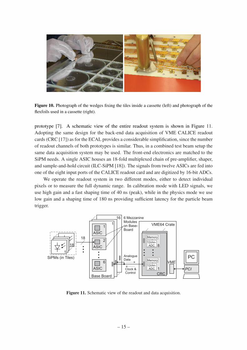
Figure 10. Photograph of the wedges fixing the tiles inside a cassette (left) and photograph of theflexfoils used in a cassette (right).
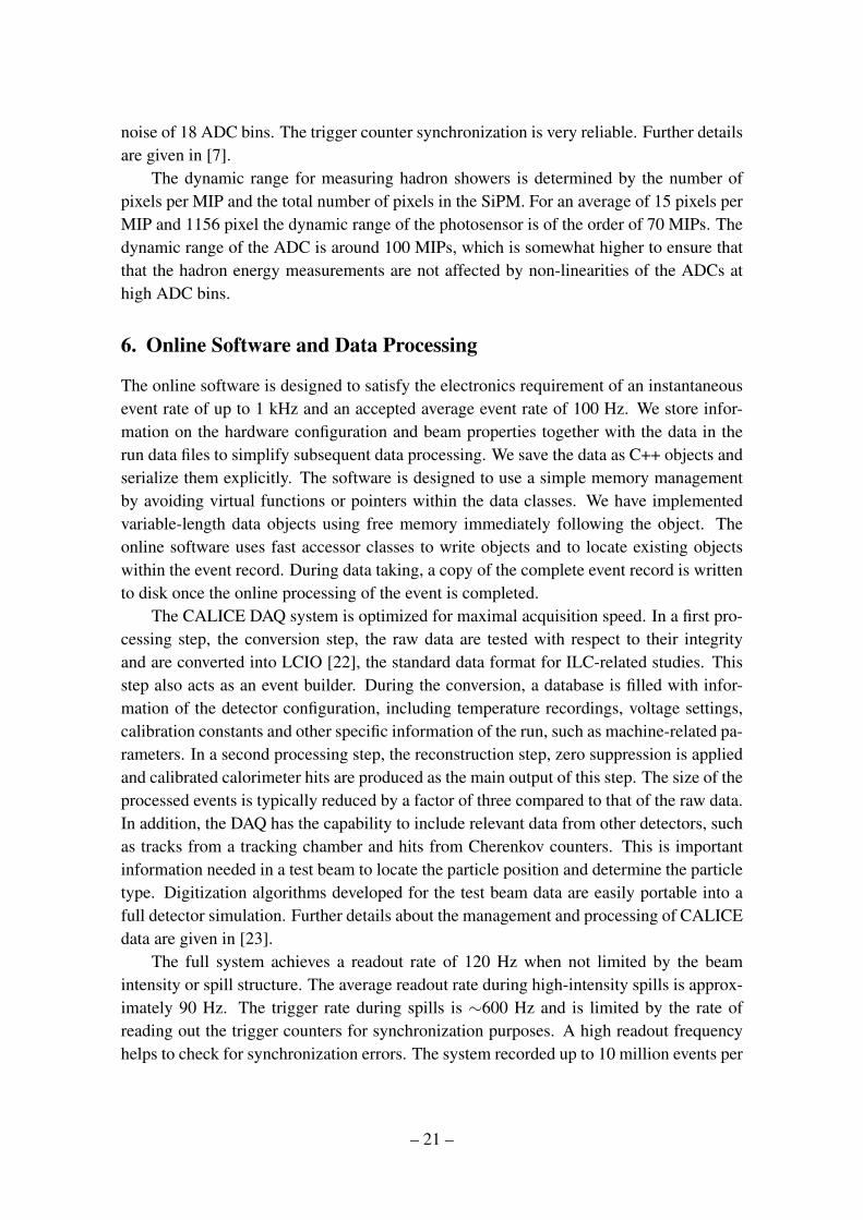
prototype [7]. A schematic view of the entire readout system is shown in Figure 11.Adopting the same design for the back-end data acquisition of VME CALICE readoutcards (CRC [17]) as for the ECAL provides a considerable simplification, since the numberof readout channels of both prototypes is similar. Thus, in a combined test beam setup thesame data acquisition system may be used. The front-end electronics are matched to theSiPM needs. A single ASIC houses an 18-fold multiplexed chain of pre-amplifier, shaper,and sample-and-hold circuit (ILC-SiPM [18]). The signals from twelve ASICs are fed intoone of the eight input ports of the CALICE readout card and are digitized by 16-bit ADCs.
We operate the readout system in two different modes, either to detect individualpixels or to measure the full dynamic range. In calibration mode with LED signals, weuse high gain and a fast shaping time of 40 ns (peak), while in the physics mode we uselow gain and a shaping time of 180 ns providing sufficient latency for the particle beamtrigger.
Figure 11. Schematic view of the readout and data acquisition.
– 15 –

Figure 12. Block diagram of the ASIC chip.
4.1 The Very-Front-End ASICs
The 18 channel ASIC chip is based on the readout chip for the Si-W ECAL prototypeand uses AMS 0.8µm CMOS technology [19]. A schematic view of a single channel ofthe ILC-SIPM ASIC chip is depicted in Figure 12. The integrated components allow usto select one of sixteen fixed preamplifier gain factors from 1 to 100 mV/pC, and one ofsixteen CR−RC2 shapers with shaping times from 40 to 180 ns. A 10 kΩ resistor may beadded at the preamplifier input to further delay the signal peaking time at the expense of a40% increase in noise. After shaping, the signal is held at its maximum amplitude with atrack and hold method and is multiplexed by an 18 channel multiplexer to provide a singleanalog output to the ADC. The total power consumption of the chip is around 200 mWfor a 5 V supply voltage. At the end of 2004 about 1000 ASICs were produced and werepackaged in a QFP100 case.
4.1.1 Slow and Fast Shaping, Bias Adjustment and Input Coupling of the SiPM
The ASIC is operated in two different modes due to different timing requirements forphysics events and calibration data. In physics events, the signals from each cell canvary between half a MIP and full saturation of the SiPM. In addition, the signals need tobe delayed until the trigger decision has been reached in a test beam environment. We,therefore, need the longest shaping time of 180 ns in the physics mode. On the otherhand, we obtain calibration data in dedicated runs with LED light to determine the SiPMgain. Here, we minimize the shaping time and use the highest amplification from thepreamplifier in order to achieve the optimum signal-to-noise ratio. The pulse shapes in the
– 16 –

calibration mode and the physics mode are shown in Figure 13. In the calibration mode,the measurements are performed without the input resistor.
The SiPM is directly connected to the chip as shown in Figure 14. In order to adjustthe reverse bias voltage of the SiPMs individually, an eight-bit DAC is placed directlyat the preamplifier input. Except for high voltage decoupling and cable matching of the50 Ω components no external circuitry is needed. The layout of the ASIC chip itself and aphotograph are depicted in Figure 15.
time [ns]-50 0 50 100 150 200 250 300 350 400
signa
l [AU
]
-0.6-0.4-0.2
00.20.40.60.8
1
time [ns]0 500 1000 1500 2000
sign
al [a
u]-0.4
-0.2
0
0.2
0.4
0.6
0.8
1
Figure 13. Pulse shapes in the calibration mode (left) and the physics mode (right).
50
100 nF
10 pF
ASICDAC
amplifiershaper
SiPM
cable
100 nF
100k
+HV
Figure 14. Coupling diagram of the SiPM to the ASIC chip.
4.1.2 Linearity, Gain and Noise Performance
We measured linearity, gain, and noise for both operation modes. Figure 16 (left) showscharge injection measurements for different preamplifier gain settings and shaping times.Figure 16 (right) shows the deviations from linearity for operation in the physics mode.Based on these measurements we chose gain settings in the physics mode such that a
– 17 –

Figure 15. Schematic diagram (left) and photograph (right) of the ASIC chip.
linearity better than 3% was achieved for input charges up to 190 pC. This ensured thatSiPMs with pixel gains up to 106 could be recorded up to full SiPM saturation 4. Thecalibration mode covered a range up to 10 pC with a linearity of 1% or less [20].
We measured a gain of 92 mVpC in calibration mode and 8.2 mV
pC in physics mode. Wedetermined the chip noise in the calibration mode to be 1.72 mV (1.52 mV), when the inputsignal is (not) connected yielding a signal-to-noise ratio of 8.6 per fired single pixel. For aSiPM with 106 pixel gain and an average of 15 pixels per MIP we expect a signal-to-noiseratio of 12.6 for a MIP signal in physics mode [20].
During commissioning of the CERN 2006 test beam, we observed typical signal-to-noise ratios of four for single pixels and eleven for minimum ionizing muons [21]. Thelarge difference in the single-pixel signal-to-noise ratio between the measurement and theexpectation mainly results from the very short shaping time. The signal-to-noise ratiomeasured in the test beam, however, is smaller than the expectation, because most SiPMshave a gain lower than 106 and due to the short shaping time not all the signal charge iscollected.
The linearity of the 18 channels of the DAC is shown in Figure 17 (left). The non-linearity of ∼ 2% essentially results from a mismatch in current mirrors. The total rangeof 4.5 V specifies the voltage selection range of SiPMs grouped together and connected toa given base board in a single cassette. The deviation from linearity is shown in Figure 17(right) for channel zero as an example. The non-linearities of the other channels are similarin size.
4.2 The Very-Front-End Readout Boards
As shown in Figure 18, we use two different types of Very-Front-End (VFE) readoutboards to interface the SiPM outputs to the data acquisition system (DAQ). The first isa mezzanine board, called AHCAL analog board (HAB) that carries one VFE ASIC with18 SiPM input channels. The second is a base board, called AHCAL base board (HBAB)
4A gain of 196 corresponds to a charge of 160 fC
– 18 –

Figure 16. Linearity measurements of preamplifier and shaper for input capacitance of Cf =
0.1 pF, 0.2 pF, 0.4 pF, 0.8 pF and 1.5 pF (left) and residuals for operation in the physics mode(right). The dashed (red) lines show a ±0.5% deviation from linearity.
Figure 17. Measurements of the DAC linearity of 18 channels (left) and residuals for channel zero(right).
that carries up to six HABs. Each HAB provides an output driver (with a gain of two) forthe processed analog SiPM signal, contains control and configuration electronics that is setremotely by the DAQ, and provides the correct bias voltage for each SiPM. The HBABs,with dimensions of 47.5 cm×19 cm, house all control functions and configuration datafrom the DAQ to the ASICs. Two HBABs read out the 216 SiPM channels of one AH-CAL layer. The modular design of the readout and use of connectors allow us to replaceindividual boards in case of malfunction.
Both types of boards are six-layer designs with a dedicated power-ground system. Allcritical signals, especially the analog outputs of the VFE ASICs and the fast LVDS controlsignals, are routed differentially with a 120 Ω line impedance that matches the impedanceof the cable to the DAQ. The external trigger line from the DAQ used by the ASICs to holdthe current input signal is length-balanced in order to achieve synchronous sampling of allASICs. Without the SiPM connected, the VFE noise (at most 1.5 mV RMS) is dominated
– 19 –

by the ASIC noise.
Figure 18. The VFE AHCAL base board with six mezzanine boards. The connection to the SiPMsis via coaxial cables.
5. Off-Detector Readout Electronics
The off-detector electronics distributes the sample-and-hold signals required by the VFEelectronics within a latency of 180±10 ns, drives the VFE signal sequence to multiplex theanalog signal readout, digitizes the signals, and stores the data. The CRCs (see Figure 11)performing this task contain eight front-end (FE) sections that are fanned into a singleback-end (BE) section providing the interface to VME. Each FE section controls twelveVFE readout ASICs needed to read out a single layer of the AHCAL. It is equipped withtwelve 16-bit ADCs to digitize the SiPM signals. The data volume within each FE is 512bytes per event. The BE collects the digitized signals and stores them into an 8 MBytememory. Since the typical event size is 4 kByte per CRC, about 2000 events can be storedbefore readout is required.
The CRCs also handle the trigger control and distribution. The trigger logic built in theBE allows for significant complexity, since we define the trigger condition via software.We set a trigger busy signal to prevent further triggers until the digitization of the VFEanalog data is completed. We use the rising edge of the trigger signal to synchronize theentire system and derive all timing information including the time-critical sample-and-holdsignal from this edge.
The system performs as expected meeting all requirements. The sample-and-hold isdistributed on the derived 160 MHz clock within a minimum of 160 ns. This allows usto implement the rest of the latency of 180 ns as a software delay in the FE FPGA. Timejitter on this signal comes from the 6.25 ns rounding errors of the clock. The CRC noisewithout the AHCAL is only 1.4 ADC bins on average, while the VFE electronics has a
– 20 –
noise of 18 ADC bins. The trigger counter synchronization is very reliable. Further detailsare given in [7].
The dynamic range for measuring hadron showers is determined by the number ofpixels per MIP and the total number of pixels in the SiPM. For an average of 15 pixels perMIP and 1156 pixel the dynamic range of the photosensor is of the order of 70 MIPs. Thedynamic range of the ADC is around 100 MIPs, which is somewhat higher to ensure thatthat the hadron energy measurements are not affected by non-linearities of the ADCs athigh ADC bins.
6. Online Software and Data Processing
The online software is designed to satisfy the electronics requirement of an instantaneousevent rate of up to 1 kHz and an accepted average event rate of 100 Hz. We store infor-mation on the hardware configuration and beam properties together with the data in therun data files to simplify subsequent data processing. We save the data as C++ objects andserialize them explicitly. The software is designed to use a simple memory managementby avoiding virtual functions or pointers within the data classes. We have implementedvariable-length data objects using free memory immediately following the object. Theonline software uses fast accessor classes to write objects and to locate existing objectswithin the event record. During data taking, a copy of the complete event record is writtento disk once the online processing of the event is completed.
The CALICE DAQ system is optimized for maximal acquisition speed. In a first pro-cessing step, the conversion step, the raw data are tested with respect to their integrityand are converted into LCIO [22], the standard data format for ILC-related studies. Thisstep also acts as an event builder. During the conversion, a database is filled with infor-mation of the detector configuration, including temperature recordings, voltage settings,calibration constants and other specific information of the run, such as machine-related pa-rameters. In a second processing step, the reconstruction step, zero suppression is appliedand calibrated calorimeter hits are produced as the main output of this step. The size of theprocessed events is typically reduced by a factor of three compared to that of the raw data.In addition, the DAQ has the capability to include relevant data from other detectors, suchas tracks from a tracking chamber and hits from Cherenkov counters. This is importantinformation needed in a test beam to locate the particle position and determine the particletype. Digitization algorithms developed for the test beam data are easily portable into afull detector simulation. Further details about the management and processing of CALICEdata are given in [23].
The full system achieves a readout rate of 120 Hz when not limited by the beamintensity or spill structure. The average readout rate during high-intensity spills is approx-imately 90 Hz. The trigger rate during spills is ∼600 Hz and is limited by the rate ofreading out the trigger counters for synchronization purposes. A high readout frequencyhelps to check for synchronization errors. The system recorded up to 10 million events per
– 21 –

day and ran for several beam periods of months. In total, about 300 million events havebeen collected, filling approximately 30 TBytes of disk space. Further details are givenin [7].
7. The Calibration and Monitoring System
Since the SiPMs are sensitive to changes in temperature and operation voltage, we needto monitor them during test beam operations. The monitoring system needs sufficientflexibility to perform three different tasks. First, we utilize the self-calibration propertiesof the SiPMs to achieve a calibration of the ADC in terms of pixels that is needed for non-linearity corrections and for directly monitoring the SiPM gain. Second, we monitor allSiPMs during test beam operations with a fixed-intensity light pulse. Third, we cross checkthe full SiPM response function by varying the light intensity from zero to the saturationlevel [24].
We built a monitoring system that distributes UV light from an LED to each tile viaclear fibers. We use UV light to attain efficient light collection by the WLS fiber. Thepulses are 10 ns wide in order to match real signals as closely as possible. If the signalwidth becomes too long, the probability for a pixel to fire twice increases rapidly. TheLED light itself is monitored with a PIN photodiode to correct for fluctuations in the LEDlight intensity that is adjustable from the DAQ system. By varying the voltage, the LEDintensity covers the full dynamic range from zero to saturation (∼ 70 MIPs).
In addition, we use high-precision power supplies to supply the reverse-bias voltageto the SiPM. Finally, we have placed five thermosensors in each cassette that are read outregularly by a slow control system storing a time stamp and the temperature recordings ina database [25].
7.1 The Light Distribution System
Since space constraints set a limit on the total number of LEDs plus electronics in a cas-sette, we couple 19 clear fibers to one LED of which 18 fibers are routed to the scintillatortiles and one fiber is routed to a PIN photodiode. The LEDs have to produce fast, brightand uniform light signals. A standard UV LED with an emission maximum at 400 nmfulfills all our requirements. Figure 19 shows the emission spectrum of the UV LED.Measurements of the light emission pattern in a dedicated laboratory setup show that thelight variation is less than a factor of two between brightest and dimmest illuminated fiber.This is sufficient to perform gain monitoring as low as two pixels and to measure thesaturation curve at least in a region where the maximum number of firing pixels can beextrapolated from a fit. For low LED intensities we observe prominent pixel peaks in allSiPMs. When the LED intensity is increased the pixel peaks broaden and become lesswell distinguishable.
We use 10 cm to 90 cm long, clear, single-clad fibers with a diameter of 0.75 mmto transport the LED light into the tiles. We have performed aging tests of the fibers by
– 22 –

Wavelength [nm]380 390 400 410 420 430 440 450 460
Nor
mal
ized
em
issi
on in
tens
ity
0
0.2
0.4
0.6
0.8
1
1.2 LED currentAµ 20 Aµ100
10 mA
Figure 19. The emission spectrum of the UV LED.
pulsing the LED at high rate and measuring the light intensity at the end of a fiber. Thistest, which is equivalent to a ten year operation, shows no deterioration. To ascertain astraight alignment of the fibers in front of the LED, the 19 fiber ends are glued togetherinside a 1.4 cm long metal sleeve with 0.5 cm diameter. The metal sleeve is inserted intoa hole drilled into the aluminum frame of the cassette. An LED is inserted into this holefrom the other side. The LEDs are soldered first to the LED driver electronics locatedon the CMB, which is attached to the cassette frame pushing the LEDs towards the fiberbundles. On the other end, each fiber is glued to a conical aluminum mirror that is 0.7 cmin diameter and is glued to a FR4 plate reflecting the LED light onto the scintillator tileat an angle of 90 (see Section 3.5). The PIN photodiodes are also mounted on the CMBand are inserted into a hole in the cassette frame. The fiber is inserted from the other sideand is centered in the hole by a special adapter. All couplings consist of thin air gaps.This construction is rather robust providing a reliable and uniform light distribution aftermoving the cassettes into place.
7.2 Calibration and Monitoring Electronics
The CMBs contain all the electronics needed to drive the LEDs, set the gain of the pream-plifiers for the PIN photodiode signals, and read out the temperature sensors. The LEDlight amplitudes are tunable from low intensities triggering individual pixels to high in-tensities producing far over 70 MIP signals. The pulse widths are adjustable within a fewns. Here, we use a typical pulse width of 10 ns. The trigger for the pulse start is obtainedfrom the DAQ and is synchronized with the readout, while an analog signal from DAQ,(V-calib), is used to control the amplitude of LED light. We use a common steering of the
– 23 –

amplitude and the pulse-width for all LEDs.Figure 20 displays the schematic of the LED driver. Our design is particularly opti-
mized for the generation of nearly rectangular pulses, i.e. pulses with a fast rise time andfast fall time (∼ 1 ns). We have checked that the LED light emission characteristics donot change with the increase of the LED current in the range 10 µA to 10 mA. In orderto reduce light fluctuations among the LEDs we have selected a subsample with a similarlight-intensity profile for one cassette. A photograph of the CMB is depicted in Figure 21.
Since PIN photodiodes have a gain of one, we need an additional charge-sensitivepreamplifier for the PIN photodiode readout. The rest of the readout chain is the same asthat of the SiPMs. The presence of a high-gain preamplifier directly on the board in thevicinity of the power signals for LEDs, however, has turned out to be a source of crosstalk.
Another task of the CMB consists of reading out the temperature sensors via a 12 bitADC. The temperature values are sent to the Slow Control system via a CANbus interface.One CMB operates seven temperature sensors, two sensors directly located on the readoutboard and five sensors distributed across the center of the cassette. The sensors consistingof integrated circuits of type LM35DM produced by National Semiconductor are placed ina 1.5 mm high SMD socket. Their absolute accuracy is < 0.6C. A microprocessor of thePIC 18F448 family in association with a CAN controller interface, PCA82C250, providesthe communication of the CMB with the Slow Control system. We have not observed anynoise pickup in the CMB.
During test beam operations, we take sets of special runs to scan the SiPM responsefunction, perform gain calibrations with low-intensity LED light, determine the electron-ics intercalibration between operation in calibration mode and physics mode, and recordthe LED reference signals and pedestals between spills. LED amplitudes for readout inhigh-gain mode and low-gain mode have been optimized individually for each module toprovide sufficient points for the gain calibration and to record the response curves. In ad-dition, all twelve LEDs in one module (one CMB) are manually tuned to deliver the sameamount of light to ensure that all SiPM signals show single-pixel peaks. All adjustmentshave been performed after complete module assembly. First tests were obtained using thefull data acquisition chain in a special test installation at the DESY electron test beam.After tuning of the LED monitoring system the efficiency for successful gain calibrationson all modules is around 98%. This includes a few broken LEDs and noisy SiPMs forwhich the single photoelectron peak spectrum cannot be fitted to extract a gain value.
8. Calibration Procedure
We calibrate each cell to the MIP scale by
Ei [MIP] =Ai [ADC]
CMIPi
· f−1i
(Ag
i [ADC]
Cpixeli
), (8.1)
– 24 –

Figure 20. Layout of the LED driver.
Figure 21. Photograph of the calibration and monitoring board.
where Ai [ADC] (Agi [ADC] ) is the pedestal subtracted energy measured for physics (cal-
ibration) events in units of ADC bins for cell i, CMIPi is a conversion factor of ADC bins
into MIPs, the function fi is the SiPM response function describing the SiPM output signalas a function of the incoming light intensity, and Cpixel
i is a conversion factor of ADC binsinto units of a single avalanche in a SiPM pixel that includes the intercalibration constant.
We extract the MIP conversion factors CMIPi of each cell using the most probable
– 25 –

2 x gain
[fired pixels]0 1 2 3 4 5
250
200
150
100
50
0
Entr
ies
Figure 22. Left: Distribution of single pixel peaks measured in the gain calibration. The super-imposed curve is a fit with multiple Gaussian functions. Right: The MIP distribution of muonsmeasured in a cell in the physics mode. The superimposed curve is a fit to a Landau distributionconvolved with a Gaussian function. The noise spectrum is shown as a reference.
response to the approximately minimum ionizing muons. A typical MIP spectrum togetherwith the pedestal spectrum of the same channel is shown in Figure 22 (right). In thesummed shower energy, we consider only cells in which the energy exceeds half a MIP.This eliminates most of the electronic noise, while keeping a high efficiency for singleparticles.
We measured the response function fi of each SiPM on the test bench before instal-lation (see Figure 5 right). The inverse function f−1
i is used to correct for non-linearitiesin the response. In future, these measurements could be replaced by regularly updatedin-situ measurements providing improved non-linearity corrections. A typical calibrationspectrum is depicted in Figure 22 (left). The inverse response function f−1
i (Ai [ADC]) isnearly one for small measured energies increasing approximately exponentially towardshigher energies. In the range of our operation the maximum correction factor does notexceed three. The conversion from the MIP scale to the GeV scale is achieved using testbeam data of known energies.
9. Commissioning and Initial Performance
Commissioning started with modules without absorber plates in a DESY electron beam.In a dedicated setup we have tested up to four modules with 3 GeV electrons. We havedetermined a first MIP calibration and have measured the in situ light yield by combiningthe MIP calibration and gain calibration. Furthermore, we have tested the non-linearitycorrection with additional absorber material in front of the module under study. Theseinitial studies were performed to establish the readout, calibration and monitoring of the7608 SiPMs used in the AHCAL prototype.
9.1 Test of Single Modules
Using the initial test beam setup at DESY we have measured energies up to ∼40 MIPs per
– 26 –

Figure 23. Left: Comparison of SiPM readout and PM readout for a 5 GeV e+ beam showeringin a 5 X0 thick lead absorber for uncorrected data (crosses), corrected data (solid points) and aGEANT3 simulation (squares); Right: Residuals of the SiPM data and simulation for uncorrected(crosses) and corrected data (solid points).
tile. We have compared the performance of the SiPM readout with that of a photomultiplier(PM) readout using a specially equipped cassette. For the latter setup we used long WLSfibers that were routed from the scintillator tiles to the outside of the module where thePMs were located. We positioned a lead absorber plate of variable thickness on the beamline in front of the module in order to initiate an electromagnetic shower. Figure 23 (leftplot) shows the correlation of the energy collected by the reference scintillator-PM systemto the energy recorded with the tile-SiPM system for a 5 GeV e+ beam showering ina 5 X0 thick lead absorber. For energies above 15 MIPs the uncorrected data (crosses)show a clear deviation from a GEANT3 simulation (squares) [26]. The largest fractionof energies in the shower maximum lies in the range between 15 and 35 MIPs, wherethe simulation deviates from the data by 10− 25%. After correcting the SiPM signalson an event-by-event basis using the measured response function (see Equation 8.1), thesimulation and the data show good agreement. This is depicted in Figure 23 (right plot)displaying the residual of the corrected data with respect to the simulation.
9.2 Test Beam Setup at CERN
The test beam setup at CERN in the H6 area started in 2006 with up to 23 modules in-stalled. In 2007 the full AHCAL prototype was completed and installed. Figure 24 showsthe setup during 2006 and 2007 test beam. Data taking was carried out with a Si-W ECALupstream and the TCMT downstream of the AHCAL. The 2006 data provide importanttests and a validation of calibration and monitoring procedures. We can also use them toperform first studies of hadron shower shapes. The 2007 data, taken with the completed
– 27 –

AHCAL prototype, allow us to perform the full program.All detectors, beam monitoring devices and the DAQ itself showed a very high relia-
bility. The uptime of the total system during test beam was > 95 %. During the two testbeam periods we collected more than 2.5×10⁸ events without zero suppression. We col-lected large samples of µ±, e± and hadrons (h±). We collected showers in the 6–80 GeV(6–45 GeV) energy range for h± (e±). Figure 25 (right plot) summarizes the event collec-tion rate during the 2006 and 2007 test beam periods.
Figure 24. CALICE calorimeter system setup at CERN in 2006 (left) and 2007 (right).
Figure 25. Event collection rate during test beam in 2006 (left) and 2007 (right).
9.3 MIP Calibration
The calibration of each cell is accomplished with muons from a beam that has a sufficientlybroad distribution to cover the entire front face of the AHCAL. A minimum of 2000 muonevents per cell is necessary to obtain a reliable fit to the pulse height spectrum that isparameterized as a convolution of a Landau distribution and a Gaussian function. Fora uniform beam distribution this amounts to a total of 5× 10⁵ events. Since the beam
– 28 –

TCMTAHCAL
ECAL
Figure 26. Three-dimensional event display of a muon from the test beam penetrating the ECAL,AHCAL and TCMT. Hits in the TCMT are indicated by the colored bars.
has a Gaussian-shaped profile, we need approximately 4× 10⁶ events to achieve a goodcalibration in the outermost cells. With an average data acquisition rate of 100 Hz, theMIP calibration of the entire AHCAL takes about 12 hours.
In the offline processing of the data, we apply muon quality selection criteria to rejectnoise events and non-muon triggers. We define a muon as a track having at least Nmin
hits within a cylinder of radius Rtile, where Nmin is the minimum number of acceptedhits that have a pulse height larger than half a MIP, based on the initial calibration. Thevalue of Rtile is chosen to be the same for each of the three tile sizes. Figure 26 showsa one-event display of a 32 GeV/c muon that passed our track selection for Nmin = 16.Figure 22 (right plot) displays a typical energy spectrum in a 3 cm× 3 cm calorimetercell measured with selected muons. The fit shown represents a Landau distribution for theenergy loss convolved with a Gaussian function to account for the system noise and thePoisson statistics introduced by the SiPM response. The most probable value of the fitfunction is defined to be the MIP calibration factor. In order to reduce a possible bias fromour track selection, we fit only the part of the spectrum that lies above the noise threshold.
Figure 27 (left plot) shows the MIP detection efficiency of calibrated cells per moduleafter imposing a minimal threshold of half a MIP. The band indicates the spread (RMS) ofall cells in one module. We determine an average efficiency of 93% that lies slightly belowour expectation of 95%. The reduced detection efficiency, however, is consistent with thefact that the calorimeter was operated at a working point of 13 pixels/MIP instead of thedesign value of 15 pixels/MIP. Figure 27 (right plot) shows the average signal-to-noiseratio for the MIP signal in each module. We measure an average signal-to-noise ratio inthe entire calorimeter of ∼10. Figure 28 shows the light yields measured in the 2006 and
– 29 –

Figure 27. Average MIP detection efficiency in each calorimeter layer (left). Average signal-to-noise ratio in each calorimeter layer for a MIP signal (right). The bands indicates the spread amongthe tiles in one layer.
Figure 28. Recorded light yields in the test beam.
2007 test beam data. The discrepancy between the measurements at ITEP and in the testbeam are due to different operating conditions.
9.4 Noise and Occupancy
An adjustment of the bias voltage for the entire AHCAL prototype is necessary in orderto set the light yield to 15 pixels/MIP and in turn to minimize the noise above threshold.If the reverse bias voltage is set too low, the number of pixels per MIP is reduced. Inturn, if the threshold is lowered the noise level increases. If, on the other hand, the re-verse bias voltage is set too high, the SiPM dark current increases and in turn the noiserises. The optimization procedure allows us to compensate for light yield changes due tolarge temperature variations (about 57 mV/K). The SiPM operation voltage specified dur-ing production is referred to as nominal voltage (∆ HV = 0 V). The SiPM noise behavior
– 30 –

with operation voltage leads to an optimization range of ±1 V. This is sufficient to com-pensate for differences between ambient temperature at the test beam and during the SiPMproduction tests. Figure 29 shows the distributions of total energy (left plot) and numberof hits (right plot) for noise (random triggers), for MIP signal measured in muon-inducedevents, and for their combination. While the noise spectra are obtained by summing theentire calorimeter for random triggers, the MIP-only spectrum is obtained by selectingonly cells through which the muon passed. By requiring a threshold of half a MIP in eachchannel the noise is negligible. It should be noted that the MIP position depends on thetotal number of layers while the noise depends on the volume of the AHCAL.
E [GeV]0 0.5 1 1.5 2 2.5
# e
ntr
ies
0
0.05
0.1
0.15HCAL: MIP+noise
HCAL: noise MPV = 0.09 GeV
HCAL: MIP MPV = 0.81 GeV
# hits
0 10 20 30 40 50 60 70
# e
ntr
ies
0
0.05
0.1
0.15
0.2 HCAL: MIP+noise
HCAL: noise mean = 4.3 hits
HCAL: MIP mean = 21.9 hits
Figure 29. Distributions of total energy (left) and number of hits (right) for noise (red solid his-togram), MIP spectra (unshaded blue histogram), and their combination (dark-shaded black) in theAHCAL. The area of the distributions are normalized to one.
An increase in the reverse bias voltage yields an increase in both gain and noise. Theeffective noise at half a MIP, however, reaches a minimum before rising again. This isshown in Figure 30 for the 2006 data, where we optimized the effective noise. For the2007 data, we optimized the light yield instead to achieve a homogeneous light yield inthe entire calorimeter resulting in an increase in noise levels. In 2006, the average noiselevel per cell was 0.9×10⁻³. In 2007, it increased to 1.3–2×10⁻³, which is about a factorof ten higher than the design goal of 10−4.
In the entire AHCAL prototype about 2 % of all cells are unusable for data analysis.Initially, modules 1 and 2 that were assembled with the very first batch of SiPMs developedhigh-noise problems because a coating layer on the silicon surface was missing. Dustparticles caused shorts to develope frequently between the poly-silicon resistor and thealuminum bus. The affected pixels drew high current creating sources for high noise inthese devices. The problem was identified in test bench studies and the subsequent SiPM
– 31 –

production was modified accordingly. The SiPMs in modules 1 and 2 were exchangedbetween the 2006 and 2007 test beam operations. In the remaining modules, only 0.2% ofthe channels suffer from a long-discharge behavior. A revised quality control procedureon the test bench allowed us to achieve such a small fraction of unusable cells.
10
15
20
25
30
35
40
-0.4 -0.2 0 0.2 0.4 0.6 0.8 1V - V [V]bias nominal
nois
e hi
ts o
n 13
mod
ules
Figure 30. Noise hits as a function of reverse bias voltage with a threshold of half a MIP.
9.5 Performance of the SiPMs in the Test Beam
The performance of the 7608 SiPMs has been studied in three test beam periods, July 2007,May 2008 and July 2008. The pedestal distribution is an excellent indicator for working,non-functioning or noisy SiPMs. The pedestal RMS of all SiPMs for runs between July2007 and July 2008 is shown in Figure 31.
The left peak corresponds to channels without electrical connection to SiPMs. Forthese channels the width of the pedestal distribution is about 18 ADC bins due to electron-ics noise. About 2% of all SiPMs fall into this category because of initially bad solderingand subsequent broken connections caused by slight deformation of the PCB to which theSiPM leads are soldered. Such deformations occurred during detector movements. Forexample 43 SiPMs became disconnected after transport from CERN to FNAL. By the endof July 2008, we found that 87 SiPMs had become disconnected permanently, and 115SiPMs had intermittent disconnections.
The distribution of the pedestal RMS does not change within periods of constant re-verse bias voltage. Three periods with different reverse bias voltage are clearly seen inFigure 31. In addition, a spike during runs 25 and 26 is caused by the adjustment periodof the reverse bias voltage. The average pedestal RMS values are 35, 37 and 40 ADCbins for the three periods that used different reverse bias voltages. These widths are muchsmaller than the typical distance between photoelectron peaks of 300–400 ADC bins and
– 32 –

Pedestal RMS [ADC bins]
# Si
PM p
er R
MS
bin
Run
num
ber
(Jul
y 20
07-Ju
ly 2
008)
Figure 31. SiPM noise during two years of operation in test beams. The pedestals are generallybetween 20 and 60 ADC bins and the number with a given pedestal RMS is stable with time
do not affect the SiPM gain calibration. In nine SiPMs the gain cannot be determined. Thiscorresponds to 0.11% of all channels. We also have a few SiPMs which show a sizableincrease of the pedestal RMS with time but they are still usable. Thus, we can concludethat the SiPMs in the AHCAL demonstrate excellent performance and stability during fourmonths of operation in 2007–2008. The number of unusable SiPMs is at the per-mil level.The soldering problem is a separate issue which will be fixed in the next prototype.
9.6 Event Displays
In order to demonstrate that the AHCAL prototype is capable of measuring the hadronicshower structure, Figure 32 shows a three-dimensional view (left) and a side view (right)of a pion shower that started in the AHCAL after leaving a track-like signature in theECAL. The display illustrates the excellent imaging potential of the AHCAL and we areconfident that this will allow us to test rigorously simulation models and reconstructionalgorithms.
10. Conclusion
We have constructed a 38-layer steel-scintillator tile analog hadron calorimeter prototypethat has a total thickness of 5.3 λn (4.3λπ ). This is the first detector that uses many
– 33 –

Figure 32. Event displays of a 20 GeV/c pion from the online monitor, showing a three dimensionalview (left) and a side view (right). The beam is coming from the right-hand side. The shower startsin the middle of AHCAL. Hits in the TCMT are indicated by the colored bars.
thousands of SiPMs for readout. The non-linearity of the SiPMs can be reliably cor-rected. Commissioning and operation in the test beam at CERN have demonstrated thatthe calorimeter performs according to expectations. The two beam-test periods show theoperational stability and robustness of the AHCAL. The high granularity gives us an ex-cellent opportunity for studying hadronic shower shapes in great detail. We anticipate thatthe results of such studies, in combination with detailed simulations, will demonstrate theextent to which nearby particle showers can be separated from one another, and henceprovide a direct test of the performance that may ultimately be achieved using the particleflow approach.
11. Acknowledgments
We would like to thank the technicians and the engineers who contributed to the design andconstruction of the prototypes, in particular P. Smirnov. We express our gratitude to theDESY, CERN and FNAL laboratories for hosting our test beam experiments, and to theirstaff for the efficient accelerator operation and excellent support. We would like to thankthe HEP group of the University of Tsukuba for the loan of drift chambers for the DESYtest beam. The authors would like to thank the RIMST (Zelenograd) group for their helpand sensors manufacturing. This work was supported by the Bundesministerium für Bil-dung und Forschung, Germany; by the DFG cluster of excellence ’Origin and Structure ofthe Universe’ of Germany; by the Helmholtz-Nachwuchsgruppen grant VH-NG-206; bythe BMBF, grant no. 05HS6VH1; by the Alexander von Humboldt Foundation (ResearchAward IV, RUS1066839 GSA); by joint Helmholtz Foundation and RFBR grant HRJRG-002, Russian Agency for Atomic Energy, ISTC grant 3090; by the Norwegian ResearchCouncil; by joint Helmholtz Foundation and RFBR grant HRJRG-002, SC Rosatom; by
– 34 –

Russian Grants SS-1329.2008.2 and RFBR08-02-12100-OFI and by the Russian Ministryof Education and Science contract 02.740.11.0239; by CICYT,Spain; by CRI(MST) ofMOST/KOSEF in Korea; by the US Department of Energy and the US National ScienceFoundation; by the Ministry of Education, Youth and Sports of the Czech Republic un-der the projects AV0 Z3407391, AV0 Z10100502, LC527 and by the Grant Agency ofthe Czech Republic under the project 202/05/0653; and by the Science and TechnologyFacilities Council, UK.
References
[1] J.-C. Brient and H. Videau, Proc. of APS/DPF/DBP summer study on the future of particlephysics, Snowmass, Colorado, 2002, arXiv hep-ex/0202004 (2002); V.L. Morgunov, Proc ofInt. Conf. on Calorimetry (Calor02), Pasadena, 70 (2002); S. Magill, New. J. Phys. 9, 409(2007).
[2] M.A. Thomson, arXiv:0907.3577 (2005); M.A.Thomson, arXiv:0907.3577 (2009), Nucl.Instrum. Meth. A 610, 2540 (2009).
[3] https://twiki.cern.ch/twiki/bin/view/CALICE/WebHome.
[4] G. Bondarenko el al., Nucl. Instrum. Meth. A 442, 187 (2000).
[5] P. Buzhan el al., Proc. of the 7th Int. Conf. on Advance Technology & Particle Physics, 717(2002).
[6] P. Buzhan el al., Nucl. Instrum. Meth. A 504, 48 (2003).
[7] J. Repond et al. (CALICE collaboration), JINST 3, P08001 (2008).
[8] R. Abrams et al, FERMILAB-CONF-07-589-E, Nov 2007. 5 (2007).
[9] LDC group, Detector outline document for the large detector concept (2007),http://www.ilcldc.org/documents/dod/.
[10] Letter of Intent of the International Detector Concept, (2009),http://www-flc.desy.de/ildloi/.
[11] E. Garutti el al., LC-DET-2006-007 (2006).
[12] V. Andreev et al., Nucl. Instr. Meth. A 540, 368 (2005).
[13] V. Morgunov and A. Raspereza, Proc. Int. Conf. Linear Colliders (LCWS04),arXiv:physics/0412108 (2004).
[14] C. Amsler et al. (Particle Data Group), Phys. Lett. B667, 1 (2008).
[15] K. Francis, PhD thesis, NIU in preparation (2010).
[16] V. Korbel, Nucl. Instrum. Meth. A 518, 49 (2004).
– 35 –

[17] P. D. Dauncey, proc. Int Conf. Linear Collider (LCWS02) arXiv:hep-ex/0211052 (2002);(LCWS2004), arXiv:hep-ex/0410001 (2004).
[18] S. Manen et al., physics/0501063 (2005).
[19] F. Wanlass, U.S. patent #3 356, 858 (1963).
[20] B. Lutz, (Hamburg U.). DESY-THESIS-2006-038, May 2006.
[21] M. Groll, (Hamburg U.). DESY-THESIS-2007-018, May 2007.
[22] F. Gaede et al. LC-TOOL-2003-053, http://www-flc.desy.de/lcnotes.
[23] R. Poeschl, Eudet-Memo-2007-57 Calice Data Processing.
[24] N. Wattimena, DESY-THESIS-2006-039 (2006).
[25] S. Karstensen, AHCAL Slow Control,http://www.desy.de/ sven/projects/hcal/hcal.html.
[26] R. Brun et al., CERN-DD/EE/84-1 (1987).
– 36 –