Embed Size (px)
Citation preview

Power Supply
RST
SC
K
Advanced
Segment
DAC
Modulator
IOUTL+
IOUTL-
IOUTR-
IOUTR+
Bias
and VREF
VCOML
VCOMR
AG
ND
2
VD
D
VC
C1
VC
C2
L
VC
C2
R
AG
ND
1
I/V and Filter
x8
Oversampling
Digital Filter
and
Function Control
Audio
Data Input
I/F
LRCK
BCK
DATA
MDO
MDI
MC
MS
AG
ND
3L
AG
ND
3R
DG
ND
Current
Segment
DAC
IREF
VOUTL
I/V and Filter
VOUTR
Function
Control I/F
MSEL
Zero
Detect
ZEROL
ZEROR
System
Clock
Manager
Current
Segment
DAC
Product
Folder
Sample &Buy
Technical
Documents
Tools &
Software
Support &Community
PCM1795SLES248A –MAY 2009–REVISED MARCH 2015
PCM1795 32-Bit, 192-kHz Sampling, Advanced Segment,Stereo Audio Digital-to-Analog Converter
1 Features 3 DescriptionThe PCM1795 device is a monolithic CMOS
1• 32-Bit Resolutionintegrated circuit that includes stereo digital-to-analog• Analog Performance: converters (DACs) and support circuitry in a small
– Dynamic Range: 123 dB SSOP-28 package. The data converters use TI’sadvanced segment DAC architecture to achieve– THD+N: 0.0005%excellent dynamic performance and improved• Differential Current Output: 3.9 mAPP tolerance to clock jitter. The PCM1795 provides
• 8× Oversampling Digital Filter: balanced current outputs, letting the user optimizeanalog performance externally. The PCM1795– Stop-Band Attenuation: –98 dBaccepts pulse code modulation (PCM) and direct– Passband Ripple: ±0.0002 dBstream digital (DSD) audio data formats, thus
• Sampling Frequency: 10 kHz to 200 kHz providing an easy interface to audio digital signal• System Clock: 128, 192, 256, 384, 512, processors (DSPs) and decoder chips. The PCM1795
device also interfaces with external digital filteror 768 fS With Autodetectdevices such as the DF1704, DF1706, and the• Accepts 16-, 24-, and 32-Bit Audio DataPMD200 from Pacific Microsonics™. Sampling rates
• PCM Data Formats: Standard, I2S, and Left- up to 200 kHz are supported. A full set of user-Justified programmable functions is accessible through an SPI
or I2C serial control port that supports register write• DSD Format Interface Availableand readback functions. The PCM1795 device also• Interface Available for Optional External Digitalsupports the time-division-multiplexed (TDM)Filter or DSP command and audio (TDMCA) data format.
• TDMCA or Serial Port (SPI™/I2C)• User-Programmable Mode Controls: Device Information(1)
PART NUMBER PACKAGE BODY SIZE (NOM)– Digital Attenuation:0 dB to –120 dB, 0.5-dB/Step PCM1795 SSOP (28) 10.20 mm × 5.30 mm
– Digital De-Emphasis (1) For all available packages, see the orderable addendum atthe end of the data sheet.– Digital Filter Roll-Off: Sharp or Slow
– Soft Mute Block Diagram– Zero Flag for Each Output
• Compatible With PCM1792A and PCM1796(Pins and Mode Controls)
• Dual Supply Operation:– 5-V Analog, 3.3-V Digital
• 5-V Tolerant Digital Inputs• Small SSOP-28 Package
2 Applications• A/V Receivers• SACD Players• DVD Players• HDTV Receivers• Car Audio Systems• Digital Multitrack Recorders• Other Applications Requiring 32-Bit Audio
1
An IMPORTANT NOTICE at the end of this data sheet addresses availability, warranty, changes, use in safety-critical applications,intellectual property matters and other important disclaimers. PRODUCTION DATA.

PCM1795SLES248A –MAY 2009–REVISED MARCH 2015 www.ti.com
Table of Contents7.4 Device Functional Modes........................................ 211 Features .................................................................. 17.5 Programming........................................................... 212 Applications ........................................................... 17.6 Register Maps ......................................................... 273 Description ............................................................. 1
8 Application and Implementation ........................ 374 Revision History..................................................... 28.1 Application Information............................................ 375 Pin Configuration and Functions ......................... 38.2 Typical Applications ................................................ 376 Specifications......................................................... 5
9 Power Supply Recommendations ...................... 576.1 Absolute Maximum Ratings ..................................... 510 Layout................................................................... 576.2 ESD Ratings.............................................................. 5
10.1 Layout Guidelines ................................................. 576.3 Recommended Operating Conditions....................... 510.2 Layout Example .................................................... 586.4 Thermal Information .................................................. 6
11 Device and Documentation Support ................. 596.5 Electrical Characteristics........................................... 611.1 Device Support...................................................... 596.6 Timing Requirements ................................................ 911.2 Trademarks ........................................................... 596.7 Typical Characteristics ............................................ 1011.3 Electrostatic Discharge Caution............................ 597 Detailed Description ............................................ 1711.4 Glossary ................................................................ 597.1 Overview ................................................................. 17
12 Mechanical, Packaging, and Orderable7.2 Functional Block Diagram ....................................... 17Information ........................................................... 597.3 Feature Description................................................. 18
4 Revision History
Changes from Original (May 2009) to Revision A Page
• Added Pin Configuration and Functions section, ESD Rating table, Recommended Operating Conditions table,Feature Description section, Device Functional Modes, Application and Implementation section, Power SupplyRecommendations section, Layout section, Device and Documentation Support section, and Mechanical,Packaging, and Orderable Information section ..................................................................................................................... 1
2 Submit Documentation Feedback Copyright © 2009–2015, Texas Instruments Incorporated
Product Folder Links: PCM1795
ZEROL
ZEROR
MSEL
LRCK
DATA
BCK
SCL
DGND
VDD
MS
MDI
MC
MDO
RST
V 2LCC
AGND3L
I L-OUT
I L+OUT
AGND2
V 1CC
V LCOM
V RCOM
IREF
AGND1
I R-OUT
I R+OUT
AGND3R
V 2RCC
1
2
3
4
5
6
7
8
9
10
11
12
13
14
28
27
26
25
24
23
22
21
20
19
18
17
16
15
PCM1795www.ti.com SLES248A –MAY 2009–REVISED MARCH 2015
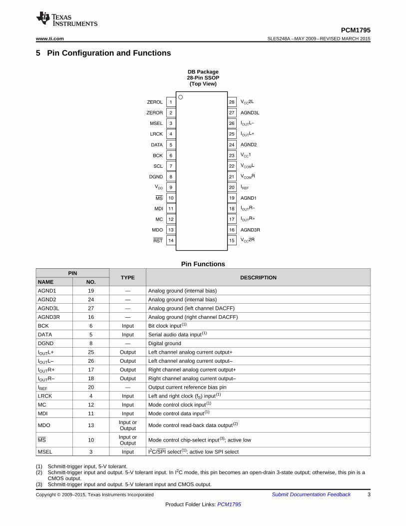
5 Pin Configuration and Functions
DB Package28-Pin SSOP(Top View)
Pin FunctionsPIN
TYPE DESCRIPTIONNAME NO.AGND1 19 — Analog ground (internal bias)AGND2 24 — Analog ground (internal bias)AGND3L 27 — Analog ground (left channel DACFF)AGND3R 16 — Analog ground (right channel DACFF)BCK 6 Input Bit clock input (1)
DATA 5 Input Serial audio data input (1)
DGND 8 — Digital groundIOUTL+ 25 Output Left channel analog current output+IOUTL– 26 Output Left channel analog current output–IOUTR+ 17 Output Right channel analog current output+IOUTR– 18 Output Right channel analog current output–IREF 20 — Output current reference bias pinLRCK 4 Input Left and right clock (fS) input (1)
MC 12 Input Mode control clock input (1)
MDI 11 Input Mode control data input (1)
Input orMDO 13 Mode control read-back data output (2)OutputInput orMS 10 Mode control chip-select input (3); active lowOutput
MSEL 3 Input I2C/SPI select (1); active low SPI select
(1) Schmitt-trigger input, 5-V tolerant.(2) Schmitt-trigger input and output. 5-V tolerant input. In I2C mode, this pin becomes an open-drain 3-state output; otherwise, this pin is a
CMOS output.(3) Schmitt-trigger input and output. 5-V tolerant input and CMOS output.
Copyright © 2009–2015, Texas Instruments Incorporated Submit Documentation Feedback 3
Product Folder Links: PCM1795

PCM1795SLES248A –MAY 2009–REVISED MARCH 2015 www.ti.com
Pin Functions (continued)PIN
TYPE DESCRIPTIONNAME NO.RST 14 Input Reset (1); active lowSCK 7 Input System clock input (1)
VCC1 23 — Analog power supply, 5 VVCC2L 28 — Analog power supply (left channel DACFF), 5 VVCC2R 15 — Analog power supply (right channel DACFF), 5 VVCOML 22 — Left channel internal bias decoupling pinVCOMR 21 — Right channel internal bias decoupling pinVDD 9 — Digital power supply, 3.3 V
Input orZEROL 1 Zero flag for left channel (3)OutputInput orZEROR 2 Zero flag for right channel (3)Output
4 Submit Documentation Feedback Copyright © 2009–2015, Texas Instruments Incorporated
Product Folder Links: PCM1795

PCM1795www.ti.com SLES248A –MAY 2009–REVISED MARCH 2015
6 Specifications
6.1 Absolute Maximum Ratings (1)
Over operating free-air temperature range, unless otherwise noted.MIN MAX UNIT
VCC1, VCC2L, VCC2R –0.3 6.5 VSupply voltage
VDD –0.3 4 VSupply voltage VCC1, VCC2L, VCC2R –0.1 0.1 VdifferencesGround voltage AGND1, AGND2, AGND3L, AGND3R, DGND –0.1 0.1 Vdifferences
LRCK, DATA, BCK, SCK, MSEL, RST, MS (2), MDI, MC, –0.3 6.5 VMDO (2), ZEROL (2), ZEROR (2)Digital input voltageZEROL (3), ZEROR (3), MDO(3), MS (3) –0.3 (VDD + 0.3) < 4 V
Analog input voltage –0.3 (VCC + 0.3) < 6.5 VInput current (any pins except supplies) –10 10 mAAmbient temperature under bias –40 125 °CJunction temperature 150 °CPackage temperature (IR reflow, peak) 260 °CStorage temperature, Tstg –55 150 °C
(1) Stresses beyond those listed under Absolute Maximum Ratings may cause permanent damage to the device. These are stress ratingsonly, and functional operation of the device at these or any other conditions beyond those indicated under Recommended OperatingConditions is not implied. Exposure to absolute-maximum-rated conditions for extended periods may affect device reliability.
(2) Input mode or I2C mode.(3) Output mode except for I2C mode.
6.2 ESD RatingsVALUE UNIT
Human body model (HBM), per ANSI/ESDA/JEDEC JS-001 (1) ±3000V(ESD) Electrostatic discharge VCharged-device model (CDM), per JEDEC specification JESD22- ±1500
C101 (2)
(1) JEDEC document JEP155 states that 500-V HBM allows safe manufacturing with a standard ESD control process.(2) JEDEC document JEP157 states that 250-V CDM allows safe manufacturing with a standard ESD control process.
6.3 Recommended Operating Conditionsover operating free-air temperature range (unless otherwise noted)
MIN NOM MAX UNITVDD Digital supply voltage 3.0 3.3 3.6 VVCC1VCC2L Analog Supply Voltage 4.7525 5 5.25 VVCC2ROperating Temperature –25 85 °C
Copyright © 2009–2015, Texas Instruments Incorporated Submit Documentation Feedback 5
Product Folder Links: PCM1795

PCM1795SLES248A –MAY 2009–REVISED MARCH 2015 www.ti.com
6.4 Thermal InformationPCM1795
THERMAL METRIC (1) DB (SSOP) UNIT28 PINS
RθJA Junction-to-ambient thermal resistance 70.3RθJC(top) Junction-to-case (top) thermal resistance 28.3RθJB Junction-to-board thermal resistance 31.5
°C/WψJT Junction-to-top characterization parameter 2.9ψJB Junction-to-board characterization parameter 31.1RθJC(bot) Junction-to-case (bottom) thermal resistance —
(1) For more information about traditional and new thermal metrics, see the IC Package Thermal Metrics application report (SPRA953).
6.5 Electrical CharacteristicsAll specifications at TA = +25°C, VCC1 = VCC2L = VCC2R = 5 V, VDD = 3.3 V, fS = 48 kHz, system clock = 256 fS, and 32-bitdata, unless otherwise noted.
PARAMETER TEST CONDITIONS MIN TYP MAX UNITRESOLUTION
Resolution 32 BitsDATA FORMAT (PCM Mode)
Audio data interface format Standard, I2S, left-justifiedAudio data bit length 16-, 24-, 32-bit selectableAudio data format MSB first, twos complement
fS Sampling frequency 10 200 kHzSystem clock frequency 128, 192, 256, 384, 512, 768 fS
DATA FORMAT (DSD Mode)Audio data interface format DSD (direct stream digital)Audio data bit length 1 Bit
fS Sampling frequency 2.8224 MHzSystem clock frequency 2.8224 11.2986 MHz
DIGITAL INPUT/OUTPUTLogic family TTL compatible
VIH 2 VDCInput logic level
VIL 0.8 VDCIIH VIN = VDD 10 μA
Input logic currentIIL VIN = 0 V –10 μAVOH IOH = –2 mA 2.4 VDC
Output logic levelVOL IOL = 2 mA 0.4 VDCDYNAMIC PERFORMANCE (PCM MODE) (1) (2)
fS = 48 kHz 0.0005% 0.001%THD+N at VOUT = 0 dB fS = 96 kHz 0.001%
fS = 192 kHz 0.0015%EIAJ, A-weighted, fS = 48 kHz 120 123
Dynamic range EIAJ, A-weighted, fS = 96 kHz 123 dBEIAJ, A-weighted, fS = 192 kHz 123
(1) Filter condition:THD+N: 20-Hz high-pass filter (HPF), 20-kHz AES17 low-pass filter (LPF)Dynamic range: 20-Hz HPF, 20-kHz AES17 LPF, A-weightedSignal-to-noise ratio: 20-Hz HPF, 20-kHz AES17 LPF, A-weightedChannel separation: 20-Hz HPF, 20-kHz AES17 LPFAnalog performance specifications are measured using the System Two™ Cascade audio measurement system by Audio Precision™ inthe averaging mode.
(2) Dynamic performance and dc accuracy are specified at the output of the post-amplifier as shown in Figure 53.
6 Submit Documentation Feedback Copyright © 2009–2015, Texas Instruments Incorporated
Product Folder Links: PCM1795

PCM1795www.ti.com SLES248A –MAY 2009–REVISED MARCH 2015
Electrical Characteristics (continued)All specifications at TA = +25°C, VCC1 = VCC2L = VCC2R = 5 V, VDD = 3.3 V, fS = 48 kHz, system clock = 256 fS, and 32-bitdata, unless otherwise noted.
PARAMETER TEST CONDITIONS MIN TYP MAX UNITEIAJ, A-weighted, fS = 48 kHz 120 123
Signal-to-noise ratio EIAJ, A-weighted, fS = 96 kHz 123 dBEIAJ, A-weighted, fS = 192 kHz 123
fS = 48 kHz 116 119Channel separation fS = 96 kHz 118 dB
fS = 192 kHz 117Level linearity error VOUT = –120 dB ±1 dB
DYNAMIC PERFORMANCE (MONO MODE) (1) (2) (3)
fS = 48 kHz 0.0005%THD+N at VOUT = 0 dB fS = 96 kHz 0.001%
fS = 192 kHz 0.0015%EIAJ, A-weighted, fS = 48 kHz 126
Dynamic range EIAJ, A-weighted, fS = 96 kHz 126 dBEIAJ, A-weighted, fS = 192 kHz 126EIAJ, A-weighted, fS = 48 kHz 126
Signal-to-noise ratio EIAJ, A-weighted, fS = 96 kHz 126 dBEIAJ, A-weighted, fS = 192 kHz 126
DSD MODE DYNAMIC PERFORMANCE (44.1 kHz, 64 fS) (1) (4)
THD+N at FS 2 V rms 0.0007%Dynamic range –60 dB, EIAJ, A-weighted 122 dBSignal-to-noise ratio EIAJ, A-weighted 122 dB
ANALOG OUTPUTGain error –7 ±2 7 % of FSRGain mismatch, channel-to-channel –3 ±0.5 3 % of FSRBipolar zero error At BPZ –2 ±0.5 2 % of FSROutput current Full-scale (0 dB) 4 mAPP
Center current At BPZ –3.5 mADIGITAL FILTER PERFORMANCE
De-emphasis error ±0.1 dB
(3) Dynamic performance and dc accuracy are specified at the output of the measurement circuit as shown in Figure 55.(4) Dynamic performance and dc accuracy are specified at the output of the post-amplifier as shown in Figure 54.
Copyright © 2009–2015, Texas Instruments Incorporated Submit Documentation Feedback 7
Product Folder Links: PCM1795

PCM1795SLES248A –MAY 2009–REVISED MARCH 2015 www.ti.com
Electrical Characteristics (continued)All specifications at TA = +25°C, VCC1 = VCC2L = VCC2R = 5 V, VDD = 3.3 V, fS = 48 kHz, system clock = 256 fS, and 32-bitdata, unless otherwise noted.
PARAMETER TEST CONDITIONS MIN TYP MAX UNITFILTER CHARACTERISTICS–1: SHARP ROLL-OFF
±0.0002 dB 0.454Passband fS–3 dB 0.49Stop band 0.546 fSPassband ripple ±0.0002 dBStop-band attenuation Stop band = 0.546 fS –98 dBDelay time 38/fS s
FILTER CHARACTERISTICS–2: SLOW ROLL-OFF±0.001 dB 0.21
Passband fS–3 dB 0.448Stop band 0.79 fSPassband ripple ±0.001 dBStop-band attenuation Stop band = 0.732 fS –80 dBDelay time 38/fS s
POWER-SUPPLY REQUIREMENTSVDD 3 3.3 3.6 VDCVCC1
Voltage rangeVCC2L 4.75 5 5.25 VDCVCC2R
fS = 48 kHz 6 8IDD fS = 96 kHz 11
fS = 192 kHz 21Supply current (5) mA
fS = 44.1 kHz 18 23ICC fS = 96 kHz 19
fS = 192 kHz 20fS = 48 kHz 110 141
mWPower dissipation (5) fS = 96 kHz 131
fS = 192 kHz 166TEMPERATURE RANGE
Operating temperature –25 +85 °C
(5) Input is bipolar zero (BPZ) data.
8 Submit Documentation Feedback Copyright © 2009–2015, Texas Instruments Incorporated
Product Folder Links: PCM1795

SDA
SCL
t(BUF) t(D-SU)
t(D-HD)
Start
t(LOW)
t(S-HD)
t(SCL-F)
t(SCL-R)
t(HI)
Repeated Start
t(RS-SU)
t(RS-HD)
t(SDA-F)
t(SDA-R) t(P-SU)
Stop
t(SP)
PCM1795www.ti.com SLES248A –MAY 2009–REVISED MARCH 2015
6.6 Timing RequirementsMIN MAX UNIT
Standard 100f(SCL) SCL clock frequency kHz
Fast 400Standard 4.7
t(BUF) Bus free time between stop and start conditions μsFast 1.3Standard 4.7
t(LOW) Low period of the SCL clock μsFast 1.3Standard 4 μs
t(HI) High period of the SCL clockFast 600 nsStandard 4.7 μs
t(RS-SU) Setup time for (repeated) start conditionFast 600 ns
t(S-HD) Standard 4 μsHold time for (repeated) start condition
t(RS-HD) Fast 600 nsStandard 250
t(D-SU) Data setup time nsFast 100Standard 0 900
t(D-HD) Data hold time nsFast 0 900Standard 20 + 0.1 CB 1000
t(SCL-R) Rise time of SCL signal nsFast 20 + 0.1 CB 300Standard 20 + 0.1 CB 1000Rise time of SCL signal after a repeated start conditiont(SCL-R1) nsand after an acknowledge bit Fast 20 + 0.1 CB 300Standard 20 + 0.1 CB 1000
t(SCL-F) Fall time of SCL signal nsFast 20 + 0.1 CB 300Standard 20 + 0.1 CB 1000
t(SDA-R) Rise time of SDA signal nsFast 20 + 0.1 CB 300Standard 20 + 0.1 CB 1000
t(SDA-F) Fall time of SDA signal nsFast 20 + 0.1 CB 300Standard 4 μs
t(P-SU) Setup time for stop conditionFast 600 ns
C(B) Capacitive load for SDA and SCL line 400 pFt(SP) Pulse duration of suppressed spike Fast 50 nsVNH Noise margin at high level for each connected device (including hysteresis) 0.2 VDD V
Figure 1. Timing Definition on the I2C Bus
Copyright © 2009–2015, Texas Instruments Incorporated Submit Documentation Feedback 9
Product Folder Links: PCM1795

0
20
40
60
80
100
120
140
160
-
-
-
-
-
-
-
-
Am
plit
ude (
dB
)
Frequency ( f )´ S
0 2 41 3
Frequency Response
Slow Roll-Off
0
2
4
6
8
10
12
14
16
18
20
-
-
-
-
-
-
-
-
-
-
Am
plit
ude (
dB
)
Frequency ( f )´ S
0 0.2 0.60.1 0.3 0.4 0.5
Transition Characteristics
Slow Roll-Off
0
20
40
60
80
100
120
140
160
-
-
-
-
-
-
-
-
Am
plit
ude (
dB
)
Frequency ( f )´ S
0 2 41 3
Frequency Response
Sharp Roll-Off
0.0005
0.0004
0.0003
0.0002
0.0001
0
0.0001
0.0002
0.0003
0.0004
0.0005
-
-
-
-
-
Am
plit
ude (
dB
)
Frequency ( f )´ S
0 0.2 0.50.1 0.3 0.4
Passband Ripple
Sharp Roll-Off
PCM1795SLES248A –MAY 2009–REVISED MARCH 2015 www.ti.com
6.7 Typical Characteristics
6.7.1 Digital Filter
Figure 2. Amplitude vs Frequency Figure 3. Amplitude vs Frequency
Figure 4. Amplitude vs Frequency Figure 5. Amplitude vs Frequency
10 Submit Documentation Feedback Copyright © 2009–2015, Texas Instruments Incorporated
Product Folder Links: PCM1795

0
1
2
3
4
5
6
7
8
9
10
-
-
-
-
-
-
-
-
-
-
De-E
mphasis
Level (d
B)
Frequency (kHz)
0 4 222 6 8 10 12
f = 48 kHzS
14 16 18 20
0.5
0.4
0.3
0.2
0.1
0
0.1
0.2
0.3
0.4
0.5
-
-
-
-
-
De-E
mphasis
Err
or
(dB
)
Frequency (kHz)
0 4 222 6 8 10 12
f = 48 kHzS
14 16 18 20
0
1
2
3
4
5
6
7
8
9
10
-
-
-
-
-
-
-
-
-
-
De-E
mphasis
Level (d
B)
Frequency (kHz)
0 4 202 6 8 10 12
f = 44.1 kHzS
14 16 18
0.5
0.4
0.3
0.2
0.1
0
0.1
0.2
0.3
0.4
0.5
-
-
-
-
-
De-E
mphasis
Err
or
(dB
)
Frequency (kHz)
0 4 202 6 8 10 12
f = 44.1 kHzS
14 16 18
0
1
2
3
4
5
6
7
8
9
10
-
-
-
-
-
-
-
-
-
-
De-E
mphasis
Level (d
B)
Frequency (kHz)
0 4 142 6 8 10 12
f = 32 kHzS
0.5
0.4
0.3
0.2
0.1
0
0.1
0.2
0.3
0.4
0.5
-
-
-
-
-
De-E
mphasis
Err
or
(dB
)
Frequency (kHz)
0 4 142 6 8 10 12
f = 32 kHzS
PCM1795www.ti.com SLES248A –MAY 2009–REVISED MARCH 2015
6.7.2 Digital Filter: De-Emphasis Filter
Figure 6. De-Emphasis Level vs Frequency Figure 7. De-Emphasis Error vs Frequency
Figure 8. De-Emphasis Level vs Frequency Figure 9. De-Emphasis Error vs Frequency
Figure 10. De-Emphasis Level vs Frequency Figure 11. De-Emphasis Error vs Frequency
Copyright © 2009–2015, Texas Instruments Incorporated Submit Documentation Feedback 11
Product Folder Links: PCM1795

126
124
122
120
118
116
Sig
nal-to
-Nois
e R
atio (
dB
)
Supply Voltage (V)
4.50 5.00 5.504.75 5.25
f = 48 kHzS
f = 192 kHzS
f = 96 kHzS
122
120
118
116
114
112
Channel S
epara
tion (
dB
)
Supply Voltage (V)
4.50 5.00 5.504.75 5.25
f = 48 kHzS f = 192 kHzS
f = 96 kHzS
0.01
0.001
0.0001
Tota
l H
arm
on
ic D
isto
rtio
n +
No
ise (
%)
Supply Voltage (V)
4.50 5.00 5.504.75 5.25
f = 48 kHzS
f = 192 kHzS f = 96 kHzS
126
124
122
120
118
116
Dynam
ic R
ange (
dB
)
Supply Voltage (V)
4.50 5.00 5.504.75 5.25
f = 48 kHzS
f = 192 kHzSf = 96 kHzS
PCM1795SLES248A –MAY 2009–REVISED MARCH 2015 www.ti.com
6.7.3 Analog Dynamic Performance: Supply Voltage CharacteristicsPCM mode, TA = +25°C, and VDD = 3.3 V; measured with circuit shown in Figure 53, unless otherwise noted.
Figure 12. THD+N vs Supply Voltage Figure 13. Dynamic Range vs Supply Voltage
Figure 14. SNR vs Supply Voltage Figure 15. Channel Separation vs Supply Voltage
12 Submit Documentation Feedback Copyright © 2009–2015, Texas Instruments Incorporated
Product Folder Links: PCM1795
0
20
40
60
80
100
120
140
160
-
-
-
-
-
-
-
-
Am
plit
ude (
dB
)
Frequency (kHz)
0 4 202 6
-60-dB Output Spectrum
BW = 20 kHz
PCM Mode
f = 48 kHz
32768 Point 8 Average
T = +25 C
V = 3.3 V
V = 5 V
S
A
DD
CC
°
8 10 12 14 16 18
0
20
40
60
80
100
120
140
160
-
-
-
-
-
-
-
-
Am
plit
ud
e (
dB
)
Frequency (kHz)
0 20 10010 30
-60-dB Output Spectrum
BW = 100 kHz
PCM Mode
f = 96 kHz
32768 Point 8 Average
T = +25 C
V = 3.3 V
V = 5 V
S
A
DD
CC
°
40 50 60 70 80 90
126
124
122
120
118
116
Sig
nal-to
-Nois
e R
atio (
dB
)
Free-Air Temperature ( C)°
-50 0 100-25 25 50 75
f = 48 kHzSf = 192 kHzS
f = 96 kHzS
122
120
118
116
114
112
Channel S
epara
tion (
dB
)
Free-Air Temperature ( C)°
-50 0 100-25 25 50 75
f = 48 kHzS
f = 192 kHzS
f = 96 kHzS
0.01
0.001
0.0001
Tota
l H
arm
on
ic D
isto
rtio
n +
No
ise
(%
)
Free-Air Temperature ( C)°
-50 0 100-25 25 50 75
f = 48 kHzS
f = 192 kHzS
f = 96 kHzS
126
124
122
120
118
116
Dynam
ic R
ange (
dB
)
Free-Air Temperature ( C)°
-50 0 100-25 25 50 75
f = 48 kHzSf = 192 kHzS
f = 96 kHzS
PCM1795www.ti.com SLES248A –MAY 2009–REVISED MARCH 2015
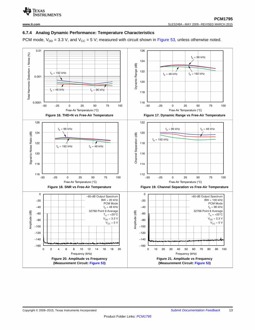
6.7.4 Analog Dynamic Performance: Temperature CharacteristicsPCM mode, VDD = 3.3 V, and VCC = 5 V; measured with circuit shown in Figure 53, unless otherwise noted.
Figure 16. THD+N vs Free-Air Temperature Figure 17. Dynamic Range vs Free-Air Temperature
Figure 18. SNR vs Free-Air Temperature Figure 19. Channel Separation vs Free-Air Temperature
Figure 20. Amplitude vs Frequency Figure 21. Amplitude vs Frequency(Measurement Circuit: Figure 53) (Measurement Circuit: Figure 53)
Copyright © 2009–2015, Texas Instruments Incorporated Submit Documentation Feedback 13
Product Folder Links: PCM1795

10
1
0.1
0.01
0.001
0.0001
Tota
l H
arm
onic
Dis
tort
ion +
Nois
e (
%)
Input Level (dBFS)
-90 -70 0-80 -60
PCM Mode
f = 48 kHz
T = +25 C
V = 3.3 V
V = 5 V
S
A
DD
CC
°
-50 -40 -30 -20 -10
0
20
40
60
80
100
120
140
160
-
-
-
-
-
-
-
-
Am
plit
ude (
dB
)
Frequency (kHz)
0 4 202 6
60-dB Output Spectrum
DSD Mode (FIR-2)
32768 Point 8 Average
T = +25 C
V = 3.3 V
V = 5 V
-
A
DD
CC
°
8 10 12 14 16 18
-120
124
128
132
136
140
144
148
152
156
160
-
-
-
-
-
-
-
-
-
-
Am
plit
ude (
dB
)
Frequency (Hz)
100 10 k1 k
-
°
144-dB Output Spectrum
BW = 20 kHz
PCM Mode
f = 48 kHz
32768 Point 8 Average
T = +25 C
V = 3.3 V
V = 5 V
S
A
DD
CC
-120
124
128
132
136
140
144
148
152
156
160
-
-
-
-
-
-
-
-
-
-
Am
plit
ude (
dB
)
Frequency (Hz)
100 10 k1 k
-
°
150-dB Output Spectrum
BW = 20 kHz
PCM Mode
f = 48 kHz
32768 Point 8 Average
T = +25 C
V = 3.3 V
V = 5 V
S
A
DD
CC
PCM1795SLES248A –MAY 2009–REVISED MARCH 2015 www.ti.com
Analog Dynamic Performance: Temperature Characteristics (continued)
Figure 22. Amplitude vs Frequency Figure 23. Amplitude vs Frequency(Measurement Circuit: Figure 53) (Measurement Circuit: Figure 53)
Figure 24. THD+N vs Input Level Figure 25. Amplitude vs Frequency(Measurement Circuit: Figure 53) (Measurement Circuit: Figure 54)
14 Submit Documentation Feedback Copyright © 2009–2015, Texas Instruments Incorporated
Product Folder Links: PCM1795

0
1
2
3
4
5
6
-
-
-
-
-
-
Gain
(dB
)
Frequency (kHz)
0 100 20050 150
DSD Filter-3
Low Bandwidth
0
10
20
30
40
50
60
-
-
-
-
-
-
Gain
(dB
)
Frequency (Hz)
0 1 M 1.5 M500 k
DSD Filter-3
High Bandwidth
f = 85 kHz
Gain = 1.5 dBC
-
0
1
2
3
4
5
6
-
-
-
-
-
-
Gain
(dB
)
Frequency (kHz)
0 100 20050 150
DSD Filter-2
Low Bandwidth
0
10
20
30
40
50
60
-
-
-
-
-
-
Gain
(dB
)
Frequency (Hz)
0 1 M 1.5 M500 k
DSD Filter-2
High Bandwidth
f = 90 kHz
Gain = 0.3 dBC
0
1
2
3
4
5
6
-
-
-
-
-
-
Gain
(dB
)
Frequency (kHz)
0 100 20050 150
DSD Filter-1
Low Bandwidth
0
10
20
30
40
50
60
-
-
-
-
-
-
Gain
(dB
)
Frequency (Hz)
0 1 M 1.5 M500 k
DSD Filter-1
High Bandwidth
f = 185 kHz
Gain = 6.6 dBC
-
PCM1795www.ti.com SLES248A –MAY 2009–REVISED MARCH 2015
6.7.5 Analog FIR Filter performance in DSD ModeAll specifications at DBCK = 2.8224 MHz (44.1 kHz × 64 fS), and 50% modulation DSD data input, unlessotherwise noted.
Figure 26. Gain vs Frequency Figure 27. Gain vs Frequency (1)
Figure 28. Gain vs Frequency Figure 29. Gain vs Frequency
Figure 30. Gain vs Frequency Figure 31. Gain vs Frequency
(1) This gain is in comparison to PCM 0 dB, when the DSD input signal efficiency is 50%.
Copyright © 2009–2015, Texas Instruments Incorporated Submit Documentation Feedback 15
Product Folder Links: PCM1795

0
1
2
3
4
5
6
-
-
-
-
-
-
Gain
(dB
)
Frequency (kHz)
0 100 20050 150
DSD Filter-4
Low Bandwidth
0
10
20
30
40
50
60
-
-
-
-
-
-
Gain
(dB
)
Frequency (Hz)
0 1 M 1.5 M500 k
DSD Filter-4
High Bandwidth
f = 94 kHz
Gain = 3.3 dBC
-
PCM1795SLES248A –MAY 2009–REVISED MARCH 2015 www.ti.com
Analog FIR Filter performance in DSD Mode (continued)
Figure 32. Gain vs Frequency Figure 33. Gain vs Frequency
16 Submit Documentation Feedback Copyright © 2009–2015, Texas Instruments Incorporated
Product Folder Links: PCM1795

Power Supply
RST
SC
K
Advanced
Segment
DAC
Modulator
IOUTL+
IOUTL-
IOUTR-
IOUTR+
Bias
and VREF
VCOML
VCOMR
AG
ND
2
VD
D
VC
C1
VC
C2
L
VC
C2
R
AG
ND
1
I/V and Filter
x8
Oversampling
Digital Filter
and
Function Control
Audio
Data Input
I/F
LRCK
BCK
DATA
MDO
MDI
MC
MS
AG
ND
3L
AG
ND
3R
DG
ND
Current
Segment
DAC
IREF
VOUTL
I/V and Filter
VOUTR
Function
Control I/F
MSEL
Zero
Detect
ZEROL
ZEROR
System
Clock
Manager
Current
Segment
DAC
PCM1795www.ti.com SLES248A –MAY 2009–REVISED MARCH 2015
7 Detailed Description
7.1 OverviewThe PCM1795 is a 32-bit, 192 kHz, differential current output stereo DAC that comes in a 28-pin SSOP package.The PCM1795 device is software controlled through I2C or SPI, and utilizes the advanced segment DACarchitecture from TI in order to perform with a Stereo Dynamic Range of 123 dB (126 dB Mono) and SNR of 123dB (126 dB Mono) with a THD of 0.0005%. The balanced current outputs allow the user to customize the analogperformance externally.
The PCM1795 device will use the SCK input as its system clock and automatically detect the sampling rate ofthe digital audio input and has a high tolerance for clock jitter. The PCM1795 device supports both PCM andDSD formats for audio input along with the TDMA or time-division-multiplexed command and audio-data format.The internal filter can be bypassed to allow for an external digital filter to be used.
7.2 Functional Block Diagram
Copyright © 2009–2015, Texas Instruments Incorporated Submit Documentation Feedback 17
Product Folder Links: PCM1795

DATA
t(BCH)
1.4 V
BCK
LRCK
t(BCL) t(LB)
t(BCY)
t(DS) t(DH)
1.4 V
1.4 V
t(BL)
PCM1795SLES248A –MAY 2009–REVISED MARCH 2015 www.ti.com
7.3 Feature Description
7.3.1 Audio Data Interface
7.3.1.1 Audio Serial InterfaceThe audio interface port is a three-wire serial port. It includes LRCK (pin 4), BCK (pin 6), and DATA (pin 5). BCKis the serial audio bit clock, and it is used to clock the serial data present on DATA into the serial shift register ofthe audio interface. Serial data are clocked into the PCM1795 on the rising edge of BCK. LRCK is the serialaudio left/right word clock.
The PCM1795 device requires the synchronization of LRCK and the system clock, but does not need a specificphase relation between LRCK and the system clock.
If the relationship between LRCK and the system clock changes more than ±6 BCK, internal operation isinitialized within 1/fS and analog outputs are forced to the bipolar zero level until resynchronization betweenLRCK and the system clock is completed.
7.3.1.2 PCM Audio Data Formats and TimingThe PCM1795 device supports industry-standard audio data formats, including standard right-justified, I2S, andleft-justified. The data formats are illustrated in Figure 35 to Figure 37. Data formats are selected using theformat bits, FMT[2:0], in control register 18. The default data format is 32-bit I2S. All formats require binary twoscomplement, MSB-first audio data. Figure 34 and Table 1 show a detailed timing diagram for the serial audiointerface.
Figure 34. Audio Interface Timing
Table 1. Serial Audio Interface Timing Characteristics for Figure 34MIN MAX UNIT
t(BCY) BCK pulse cycle time 70 nst(BCL) BCK pulse duration, low 30 nst(BCH) BCK pulse duration, high 30 nst(BL) BCK rising edge to LRCK edge 10 nst(LB) LRCK edge to BCK rising edge 10 nst(DS) DATA setup time 10 nst(DH) DATA hold time 10 ns
LRCK clock data 50% ± 2 bit clocks
18 Submit Documentation Feedback Copyright © 2009–2015, Texas Instruments Incorporated
Product Folder Links: PCM1795

1 2 32 211 2 32
21
LSB
1 2 24 1 2 2423
31
BCK
Left Channel
DATA
Right Channel
1/fSLRCK
Audio Data Word = 32-Bit, BCK 64 f³ S
DATA
Audio Data Word = 24-Bit, BCK 48 f³ S
MSB
LSBMSB
23
31
21
MSB LSB
1 2 24 1 2 24
BCK
Left Channel
DATA
Right Channel
1/fS
LRCK
Audio Data Word = 24-Bit, BCK 48 f³ S
23 23
14 15 16 1 2 15 16
MSB LSB
1 2 15 16
22 23 24 1 2 23 24 1 2 23 24
30 31 32 1 312 32 1 312 32
BCK
Left Channel
DATA
Right Channel
1/fS
DATA
DATA
LRCK
Audio Data Word = 16-Bit, BCK 32 f³ S
Audio Data Word = 24-Bit, BCK 48 f³ S
Audio Data Word = 32-Bit, BCK 64 f³ S
MSB LSB
MSB LSB
PCM1795www.ti.com SLES248A –MAY 2009–REVISED MARCH 2015
Figure 35. Audio Data Input Format: Standard Data Format (Right-Justified), Left Channel = High, RightChannel = Low
Figure 36. Audio Data Input Format: Left-Justified Data Format, Left Channel = High, Right Channel =Low
Figure 37. Audio Data Input Format: I2S Data Format, Left Channel = Low, Right Channel = High
Copyright © 2009–2015, Texas Instruments Incorporated Submit Documentation Feedback 19
Product Folder Links: PCM1795
0
1
2
3
4
5
6
-
-
-
-
-
-
Outp
ut C
urr
ent (m
A)
OUTPUT CURRENT vs INPUT CODE
I NOUT
I POUT
Input Code (Hex)
80000000 ( FS)- 000000 (BPZ) 7FFFFFFF (+FS)
PCM1795SLES248A –MAY 2009–REVISED MARCH 2015 www.ti.com
7.3.1.3 External Digital Filter Interface and TimingThe PCM1795 device supports an external digital filter interface that consists of a three- or four-wiresynchronous serial port that allows the use of an external digital filter. External filters include the TexasInstruments’ DF1704 and DF1706, the Pacific Microsonics PMD200, or a programmable digital signal processor.
In the external DF mode, LRCK (pin 4), BCK (pin 6) and DATA (pin 5) are defined as: WDCK, the word clock;BCK, the bit clock; and DATA, the monaural data. The external digital filter interface is selected by using theDFTH bit of control register 20, which functions to bypass the internal digital filter of the PCM1795 device .
When the DFMS bit of control register 19 is set, the PCM1795 device can process stereo data. In this case,ZEROL (pin 1) and ZEROR (pin 2) are defined as left-channel data and right-channel data input, respectively.
Detailed information for the external digital filter interface mode is provided in Application For External DigitalFilter Interface.
7.3.1.4 Direct Stream Digital (DSD) Format Interface and TimingThe PCM1795 device supports the DSD format interface operation, which includes out-of-band noise filteringusing an internal analog FIR filter. For DSD operation, SCK (pin 7) is redefined as BCK, DATA (pin 5) as DATAL(left channel audio data), and LRCK (pin 4) as DATAR (right channel audio data). BCK (pin 6) must be forcedlow in the DSD mode. The DSD format interface is activated by setting the DSD bit of control register 20.
Detailed information for the DSD mode is provided in Application For DSD Format (DSD Mode) Interface.
7.3.1.5 TDMCA InterfaceThe PCM1795 device supports the time-division-multiplexed command and audio (TDMCA) data format toenable control of and communication with a number of external devices over a single serial interface.
Detailed information for the TDMCA format is provided in TDMCA Interface Format.
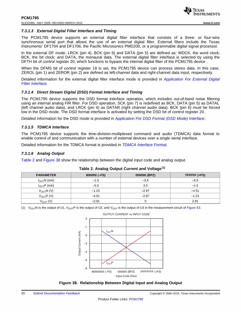
7.3.1.6 Analog OutputTable 2 and Figure 38 show the relationship between the digital input code and analog output.
Table 2. Analog Output Current and Voltage (1)
PARAMETER 800000 (–FS) 000000 (BPZ) 7FFFFF (+FS)IOUTN (mA) –1.5 –3.5 –5.5IOUTP (mA) –5.5 3.5 –1.5VOUTN (V) –1.23 –2.87 –4.51VOUTP (V) –4.51 –2.87 –1.23VOUT (V) –2.91 0 2.91
(1) VOUTN is the output of U1, VOUTP is the output of U2, and VOUT is the output of U3 in the measurement circuit of Figure 53.
Figure 38. Relationship Between Digital Input and Analog Output
20 Submit Documentation Feedback Copyright © 2009–2015, Texas Instruments Incorporated
Product Folder Links: PCM1795

t(SCKH)
System Clock
(SCK)
t(SCKL)
2 V
0.8 V
High
Low
t(SCY)
PCM1795www.ti.com SLES248A –MAY 2009–REVISED MARCH 2015
7.4 Device Functional Modes• SPI Mode is selected by connecting MSEL to DGND. SPI mode uses four signal lines and allows higher
speed full-duplex communication between the host and the PCM1795 device.• I2C Mode is selected by connecting MSEL to VDD. I2C uses two signal lines for half-duplex communication,
and used in a variety of devices.• I2S input Mode is selected by default and is controlled by Register 20 bit 5.• DSD input Mode is selected by setting Register 20 bit 5 high.• TDMCA Mode is enabled when the PCM1795 device receives an LRCK signal with a pulse duration of two
BCK clocks.
7.5 Programming
7.5.1 System Clock and Reset Functions
7.5.1.1 System Clock InputThe PCM1795 requires a system clock to operate the digital interpolation filters and advanced segment DACmodulators. The system clock is applied at the SCK input (pin 7). The PCM1795 has a system clock detectioncircuit that automatically senses the frequency at which the system clock is operating. Table 3 shows examplesof system clock frequencies for common audio sampling rates. If the oversampling rate of the delta-sigma (ΔΣ)modulator is selected as 128 fS, the system clock frequency is required to be greater than 256 fS.
Figure 39 and Table 4 show the timing requirements for the system clock input. For optimal performance, it isimportant to use a clock source with low phase jitter and noise. The Texas Instruments PLL1700 family ofmulticlock generators is an excellent choice to provide the PCM1795 system clock.
Table 3. System Clock Rates for Common Audio Sampling FrequenciesSYSTEM CLOCK FREQUENCY (fSCK) (MHz)SAMPLING FREQUENCY
(kHz) 128 fS 192 fS 256 fS 384 fS 512 fS 768 fS
32 4.096 (1) 6.144 (1) 8.192 12.288 16.384 24.57644.1 5.6488 (1) 8.4672 11.2896 16.9344 22.5792 33.868848 6.144 (1) 9.216 12.288 18.432 24.576 36.86496 12.288 18.432 24.576 36.864 49.152 (1) 73.728 (1)
192 24.576 36.864 49.152 (1) 73.728 (1) X (2) X (2)
(1) This system clock rate is not supported in I2C fast mode.(2) This system clock rate is not supported for the given sampling frequency.
Figure 39. System Clock Input Timing
Table 4. System Clock Input Timing Characteristics for Figure 39MIN MAX UNIT
t(SCY) System clock pulse cycle time 13 nst(SCKH) System clock pulse duration, high 0.4t(SCY) nst(SCKL) System clock pulse duration, low 0.4t(SCY) ns
Copyright © 2009–2015, Texas Instruments Incorporated Submit Documentation Feedback 21
Product Folder Links: PCM1795

Reset Reset Removal
1024 System Clocks
Internal Reset
System Clock
RST (Pin 14)
t(RST)
1.4 V
Reset
1024 System Clocks
VDD
2.4 V (Max)
2 V (Typ)
1.6 V (Min)
Internal Reset
System Clock
Reset Removal
PCM1795SLES248A –MAY 2009–REVISED MARCH 2015 www.ti.com
7.5.1.2 Power-On and External Reset FunctionsThe PCM1795 includes a power-on reset function, as shown in Figure 40. With VDD > 2 V, the power-on resetfunction is enabled. The initialization sequence requires 1024 system clocks from the time VDD > 2 V. After theinitialization period, the PCM1795 is set to its default reset state, as described in Mode Control Registers.
The PCM1795 also includes an external reset capability using the RST input (pin 14). This feature allows anexternal controller or master reset circuit to force the PCM1795 to initialize to the default reset state.
Figure 41 and Table 5 show the external reset operation and timing. The RST pin is set to logic 0 for a minimumof 20 ns. The RST pin is then set to a logic 1 state, thus starting the initialization sequence that requires 1024system clock periods. The external reset is especially useful in applications where there is a delay between thePCM1795 power-up and system clock activation.
Figure 40. Power-On Reset Timing
Figure 41. External Reset Timing
Table 5. External Reset Timing Characteristics for Figure 41MIN MAX UNIT
t(RST) Reset pulse duration, low 20 ns
7.5.2 Function Descriptions
7.5.2.1 Zero DetectThe PCM1795 has a zero-detect function. When the PCM1795 detects the zero conditions as shown in Table 6,the PCM1795 sets ZEROL (pin 1) and ZEROR (pin 2) high.
22 Submit Documentation Feedback Copyright © 2009–2015, Texas Instruments Incorporated
Product Folder Links: PCM1795

MSB LSB
Register Index (or Address) Register Data
R/W IDX6 IDX5 IDX4 IDX3 IDX2 IDX1 IDX0 D7 D6 D5 D4 D3 D2 D1 D0
PCM1795www.ti.com SLES248A –MAY 2009–REVISED MARCH 2015
Table 6. Zero ConditionsMODE DETECTING CONDITION AND TIMEPCM DATA is continuously low for 1024 LRCKs.
External DF mode DATA is continuously low for 1024 WDCKs.There are an equal number of 1s and 0s in every 8 bits of DSD input data for 23DZ0 ms.DSD
DZ1 The input data are continuously 1001 0110 for 23 ms.
7.5.3 Serial Control InterfaceThe PCM1795 supports both SPI and I2C interfaces that set the mode control registers; see Table 10. The serialcontrol interface is selected by MSEL (pin 3); SPI is activated when MSEL is set low, and I2C is activated whenMSEL is set high.
7.5.3.1 SPI InterfaceThe SPI interface is a four-wire synchronous serial port that operates asynchronously to the serial audio interfaceand the system clock (SCK). The serial control interface is used to program and read the on-chip mode registers.The control interface includes MDO (pin 13), MDI (pin 11), MC (pin 12), and MS (pin 10). MDO is the serial dataoutput, used to read back the values of the mode registers; MDI is the serial data input, used to program themode registers; MC is the serial bit clock, used to shift data in and out of the control port; and MS is the modecontrol enable, used to enable the internal mode register access.
7.5.3.2 Register Read/Write OperationAll read/write operations for the serial control port use 16-bit data words. Figure 42 shows the control data wordformat. The most significant bit (MSB) is the read/write (R/W) bit. For write operations, the R/W bit must be set to'0'. For read operations, the R/W bit must be set to '1'. There are 7 bits, labeled IDX[6:0], that hold the registerindex (or address) for the read and write operations. The least significant 8 bits, D[7:0], contain the data to bewritten to, or the data that was read from, and the register specified by IDX[6:0].
Figure 43 shows the functional timing diagram for writing or reading the serial control port. MS is held at a logic 1state until a register must be written to or read from. To start the register write or read cycle, MS is set to logic 0.Sixteen clocks are then provided on MC, corresponding to the 16 bits of the control data word on MDI andreadback data on MDO. After the eighth clock cycle has completed, the data from the indexed-mode controlregister appears on MDO during the read operation. After the 16th clock cycle has completed, the data arelatched into the indexed-mode control register during the write operation. To write or read subsequent data, MSmust be set to '1' once.
Figure 42. Control Data Word Format for MDI
Copyright © 2009–2015, Texas Instruments Incorporated Submit Documentation Feedback 23
Product Folder Links: PCM1795

t(MCH)
1.4 VMS
t(MSS)
LSB
1.4 V
1.4 V
t(MCL)
t(MCY)
t(MDS)
MC
MDI
t(MOS)
50% of VDDMDO
t(MHH)
t(MSH)
t(MDH)
High Impedance
When Read Mode is Instructed
R/W A6
MS
MC
MDI
MDO
A5 A4 A3 A2 A1 A0 D7 D6 D5 D4 D3 D2 D1 D0
D7 D6 D5 D4 D3 D2 D1 D0
PCM1795SLES248A –MAY 2009–REVISED MARCH 2015 www.ti.com
NOTE: Bit 15 is used for selection of write or read. Setting R/W = 0 indicates a write, while R/W = 1 indicates a read.Bits 14–8 are used for the register address. Bits 7–0 are used for register data.
Figure 43. Serial Control Format
Figure 44. Control Interface Timing
Table 7. Control Interface Timing Characteristics for Figure 44MIN MAX UNIT
t(MCY) MC pulse cycle time 100 nst(MCL) MC low-level time 40 nst(MCH) MC high-level time 40 nst(MHH) MS high-level time 80 nst(MSS) MS falling edge to MC rising edge 15 nst(MSH) MS hold time (1) 15 nst(MDH) MDI hold time 15 nst(MDS) MDI setup time 15 nst(MOS) MC falling edge to MDO stable 30 ns
(1) MC rising edge for LSB to MS rising edge.
24 Submit Documentation Feedback Copyright © 2009–2015, Texas Instruments Incorporated
Product Folder Links: PCM1795

9
SDA
SCL St
Start
Condition
17 8 18 9 18 9 9 Sp
Stop
Condition
Slave Address ACK DATA ACK DATA ACK ACKR/W
Read Operation
Transmitter M M M S S M S M M M
Data Type St Slave Address R ACK DATA ACK DATA ACK NACK Sp
Write Operation
Transmitter M M M S M S M S S M
Data Type St Slave Address W ACK DATA ACK DATA ACK ACK Sp
R/ : Read Operation if 1; Otherwise, Write Operation
ACK: Acknowledgment of a Byte if 0
NACK: Not Acknowledged if 1
DATA: 8 Bits (Byte)
W
M: Master Device
S: Slave Device
St: Start Condition
Sp: Stop Condition
R: Read
: WriteWACK: Acknowledge
NACK: Not Acknowledged
MSB LSB
1 0 0 1 1 ADR1 ADR0 R/W
PCM1795www.ti.com SLES248A –MAY 2009–REVISED MARCH 2015
7.5.4 I2C InterfaceThe PCM1795 supports the I2C serial bus and the data transmission protocol for standard and fast mode as aslave device. This protocol is explained in the I2C specification 2.0.
In I2C mode, the control terminals are changed as described in Table 8.
Table 8. Control TerminalsTERMINAL NAME TDMCA NAME PROPERTY DESCRIPTION
MS ADR0 Input I2C address 0MDI ADR1 Input I2C address 1MC SCL Input I2C clock
MDO SDA Input/output I2C data
7.5.4.1 Slave AddressThe PCM1795 has 7 bits for its own slave address, as shown in Figure 45. The first 5 bits (MSBs) of the slaveaddress are factory preset to 10011. The next 2 bits of the address byte are the device select bits that can beuser-defined by the ADR1 and ADR0 terminals. A maximum of four PCM1795 devicess can be connected on thesame bus at one time. Each PCM1795 responds when it receives its own slave address.
Figure 45. Slave Address
7.5.4.2 Packet ProtocolA master device must control packet protocol that consists of a start condition, slave address, read/write bit, dataif write or acknowledge if read, and stop condition. The PCM1795 supports only slave receivers and slavetransmitters.
Figure 46. Basic I2C Framework
Copyright © 2009–2015, Texas Instruments Incorporated Submit Documentation Feedback 25
Product Folder Links: PCM1795
SCL
SDA
Noise
Data Type Data
Transmitter
St ACK ACK ACK
M
SpACK
M
NACKSr R
M M M S M S M M M S S M
Slave Address W Register Address Slave Address
M: Master Device
S: Slave Device
St: Start Condition
Sr: Repeated Start Condition
Sp: Stop Condition
R: Read
: WriteW
ACK: Acknowledge
NACK: Not Acknowledged
Data Type Write Data 2
Transmitter
St ACK ACK ACK
M
SpACK
S
NACK
M M M S M S M S M S
Slave Address W Register Address Write Data 1
M: Master Device
S: Slave Device
St: Start Condition
Sp: Stop Condition
ACK: Acknowledge
NACK: Not Acknowledged
: WriteW
PCM1795SLES248A –MAY 2009–REVISED MARCH 2015 www.ti.com
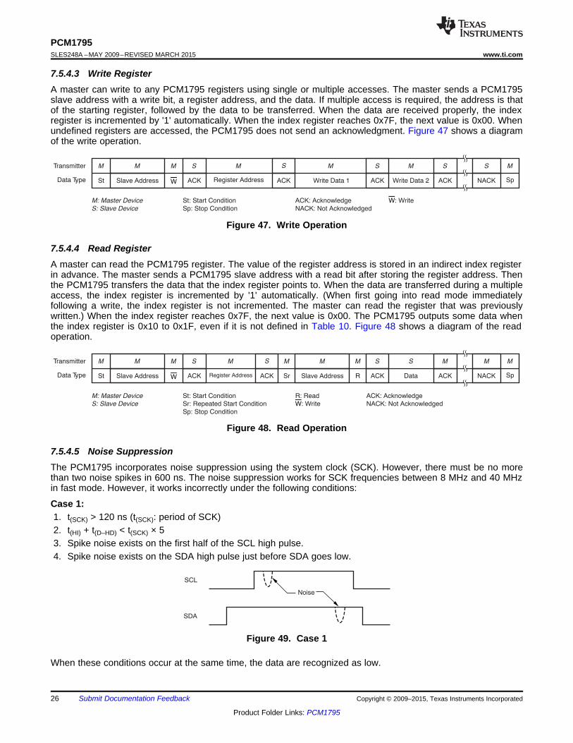
7.5.4.3 Write RegisterA master can write to any PCM1795 registers using single or multiple accesses. The master sends a PCM1795slave address with a write bit, a register address, and the data. If multiple access is required, the address is thatof the starting register, followed by the data to be transferred. When the data are received properly, the indexregister is incremented by '1' automatically. When the index register reaches 0x7F, the next value is 0x00. Whenundefined registers are accessed, the PCM1795 does not send an acknowledgment. Figure 47 shows a diagramof the write operation.
Figure 47. Write Operation
7.5.4.4 Read RegisterA master can read the PCM1795 register. The value of the register address is stored in an indirect index registerin advance. The master sends a PCM1795 slave address with a read bit after storing the register address. Thenthe PCM1795 transfers the data that the index register points to. When the data are transferred during a multipleaccess, the index register is incremented by '1' automatically. (When first going into read mode immediatelyfollowing a write, the index register is not incremented. The master can read the register that was previouslywritten.) When the index register reaches 0x7F, the next value is 0x00. The PCM1795 outputs some data whenthe index register is 0x10 to 0x1F, even if it is not defined in Table 10. Figure 48 shows a diagram of the readoperation.
Figure 48. Read Operation
7.5.4.5 Noise SuppressionThe PCM1795 incorporates noise suppression using the system clock (SCK). However, there must be no morethan two noise spikes in 600 ns. The noise suppression works for SCK frequencies between 8 MHz and 40 MHzin fast mode. However, it works incorrectly under the following conditions:
Case 1:1. t(SCK) > 120 ns (t(SCK): period of SCK)2. t(HI) + t(D–HD) < t(SCK) × 53. Spike noise exists on the first half of the SCL high pulse.4. Spike noise exists on the SDA high pulse just before SDA goes low.
Figure 49. Case 1
When these conditions occur at the same time, the data are recognized as low.
26 Submit Documentation Feedback Copyright © 2009–2015, Texas Instruments Incorporated
Product Folder Links: PCM1795

SCL
SDA
Noise
SCL
SDA
Noise
PCM1795www.ti.com SLES248A –MAY 2009–REVISED MARCH 2015
Case 2:1. t(SCK) > 120 ns2. t(S–HD) or t(RS–HD) < t(SCK) × 53. Spike noise exists on both SCL and SDA during the hold time.
Figure 50. Case 2
When these conditions occur at the same time, the PCM1795 fails to detect a start condition.
Case 3:1. t(SCK) < 50 ns2. t(SP) > t(SCK)
3. Spike noise exists on SCL just after SCL goes low.4. Spike noise exists on SDA just before SCL goes low.
Figure 51. Case 3
When these conditions occur at the same time, the PCM1795 erroneously detects a start or stop condition.
7.6 Register Maps
7.6.1 Mode Control Registers
7.6.1.1 User-Programmable Mode ControlsThe PCM1795 device includes a number of user-programmable functions that are accessed via mode controlregisters. The registers are programmed using the serial control interface, as previously discussed in SPIInterface and I2C Interface. Table 9 lists the available mode-control functions, along with the default resetconditions and associated register index.
Table 9. User-Programmable Function ControlsDF
FUNCTION DEFAULT REGISTER BIT PCM DSD BYPASS
Digital attenuation control Register 16 ATL[7:0] (for left channel)0 dB Yes No No
0 dB to –120 dB and mute, 0.5-dB step Register 17 ATR[7:0] (for right channel)
Attenuation load controlAttenuation disabled Register 18 ATLD Yes No No
Disabled, enabled
Input audio data format selection
16-, 20-, 32-bit standard (right-justified)Register 18 FMT[2:0] Yes No Yes24-bit I2S formatformat
24-bit MSB-first left-justified format16-/32-bit I2S format
Copyright © 2009–2015, Texas Instruments Incorporated Submit Documentation Feedback 27
Product Folder Links: PCM1795

PCM1795SLES248A –MAY 2009–REVISED MARCH 2015 www.ti.com
Register Maps (continued)Table 9. User-Programmable Function Controls (continued)
DFFUNCTION DEFAULT REGISTER BIT PCM DSD BYPASS
Sampling rate selection for de-emphasisDe-emphasis disabled Register 18 DMF[1:0] Yes Yes (1) No
Disabled, 44.1 kHz, 48 kHz, 32 kHz
De-emphasis controlDe-emphasis disabled Register 18 DME Yes No No
Disabled, enabled
Soft mute controlMute disabled Register 18 MUTE Yes No No
Soft mute disabled, enabled
Output phase reversalNormal Register 19 REV Yes Yes Yes
Normal, reverse
Attenuation speed selection×1 fS Register 19 ATS[1:0] Yes No No
×1fS, ×(1/2)fS, ×(1/4)fS, ×(1/8)fSDAC operation control
DAC operation enabled Register 19 OPE Yes Yes YesEnabled, disabled
Stereo DF bypass mode selectMonaural Register 19 DFMS Yes No Yes
Monaural, stereo
Digital filter roll-off selectionSharp roll-off Register 19 FLT Yes No No
Sharp roll-off, slow roll-off
Infinite zero mute controlDisabled Register 19 INZD Yes No Yes
Disabled, enabled
System reset controlNormal operation Register 20 SRST Yes Yes Yes
Reset operation, normal operation
DSD interface mode controlDisabled Register 20 DSD Yes Yes No
DSD enabled, disabled
Digital-filter bypass controlDF enabled Register 20 DFTH Yes No Yes
DF enabled, DF bypass
Monaural mode selectionStereo Register 20 MONO Yes Yes Yes
Stereo, monaural
Channel selection for monaural mode dataLeft channel Register 20 CHSL Yes Yes Yes
Left channel, Right channel
ΔΣ oversampling rate selection×64 fS Register 20 OS[1:0] Yes Yes (2) Yes
×64 fS, ×128 fS, ×32 fSPCM zero output enable Enabled Register 21 PCMZ Yes No Yes
DSD zero output enable Disabled Register 21 DZ[1:0] Yes Yes No
FUNCTION AVAILABLE ONLY FOR READ
Zero detection flag Not zero = 0 ZFGL (for left channel)Register 22 Yes Yes Yes
Not zero, zero detected Zero detected = 1 ZFGR (for right channel)
Device ID (at TDMCA) — Register 23 ID[4:0] Yes No No
(1) When in DSD mode, DMF[1:0] is defined as DSD filter (analog FIR) performance selection.(2) When in DSD mode, OS[1:0] is defined as DSD filter (analog FIR) operating rate selection.
7.6.1.2 Register MapThe mode control register map is shown in Table 10. Registers 16 to 21 include an R/W bit that determineswhether a register read (R/W = 1) or write (R/W = 0) operation is performed. Registers 22 and 23 are read-only.
Table 10. Mode Control Register MapREGISTER B15 B14 B13 B12 B11 B10 B9 B8 B7 B6 B5 B4 B3 B2 B1 B0
Register 16 R/W 0 0 1 0 0 0 0 ATL7 ATL6 ATL5 ATL4 ATL3 ATL2 ATL1 ATL0
Register 17 R/W 0 0 1 0 0 0 1 ATR7 ATR6 ATR5 ATR4 ATR3 ATR2 ATR1 ATR0
Register 18 R/W 0 0 1 0 0 1 0 ATLD FMT2 FMT1 FMT0 DMF1 DMF0 DME MUTE
Register 19 R/W 0 0 1 0 0 1 1 REV ATS1 ATS0 OPE RSV DFMS FLT INZD
28 Submit Documentation Feedback Copyright © 2009–2015, Texas Instruments Incorporated
Product Folder Links: PCM1795

Register 18 R/W 0 0 1 0 0 1 0 ATLD FMT2 FMT1 FMT0 DMF1 DMF0 DME MUTE
B15 B14 B13 B12 B11 B10 B9 B8 B7 B6 B5 B4 B3 B2 B1 B0
Register 16 R/W 0 0 1 0 0 0 0 ATL7 ATL6 ATL5 ATL4 ATL3 ATL2 ATL1 ATL0
Register 17 R/W 0 0 1 0 0 0 1 ATR7 ATR6 ATR5 ATR4 ATR3 ATR2 ATR1 ATR0
B15 B14 B13 B12 B11 B10 B9 B8 B7 B6 B5 B4 B3 B2 B1 B0
PCM1795www.ti.com SLES248A –MAY 2009–REVISED MARCH 2015
Table 10. Mode Control Register Map (continued)REGISTER B15 B14 B13 B12 B11 B10 B9 B8 B7 B6 B5 B4 B3 B2 B1 B0
Register 20 R/W 0 0 1 0 1 0 0 RSV SRST DSD DFTH MONO CHSL OS1 OS0
Register 21 R/W 0 0 1 0 1 0 1 RSV RSV RSV RSV RSV DZ1 DZ0 PCMZ
Register 22 R 0 0 1 0 1 1 0 RSV RSV RSV RSV RSV RSV ZFGR ZFGL
Register 23 R 0 0 1 0 1 1 1 RSV RSV RSV ID4 ID3 ID2 ID1 ID0
7.6.1.3 Register Definitions
7.6.1.3.1 R/W: Read/Write Mode Select
When R/W = 0, a write operation is performed.
When R/W = 1, a read operation is performed.
Default value: 0
7.6.1.3.2 ATx[7:0]: Digital Attenuation Level Setting
These bits are available for read and write.
Default value: 1111 1111b
Each DAC output has a digital attenuator associated with it. The attenuator can be set from 0 dB to –120 dB, in0.5-dB steps. Alternatively, the attenuator can be set to infinite attenuation (or mute). The attenuation data foreach channel can be set individually. However, the data load control (the ATLD bit of control register 18) iscommon to both attenuators. ATLD must be set to '1' in order to change an attenuator setting. The attenuationlevel can be set using Equation 1.Attenuation level (dB) = 0.5 dB × (ATx[7:0]DEC – 255)
where
ATx[7:0]DEC = 0 through 255 (1)
For ATx[7:0]DEC = 0 through 14, the attenuator is set to infinite attenuation. Table 11 lists the attenuation levelsfor various settings.
Table 11. Attenuation LevelsATx[7:0] DECIMAL VALUE ATTENUATION LEVEL SETTING
1111 1111b 255 0 dB, no attenuation (default)1111 1110b 254 –0.5 dB1111 1101b 253 –1.0 dB
— — —0001 0000b 16 –119.5 dB0000 1111b 15 –120.0 dB0000 1110b 14 Mute
— — —0000 0000b 0 Mute
7.6.1.3.3 R/W: Read/Write Mode Select
When R/W = 0, a write operation is performed.
Copyright © 2009–2015, Texas Instruments Incorporated Submit Documentation Feedback 29
Product Folder Links: PCM1795

PCM1795SLES248A –MAY 2009–REVISED MARCH 2015 www.ti.com
When R/W = 1, a read operation is performed.
Default value: 0
7.6.1.3.4 ATLD: Attenuation Load Control
This bit is available for read and write.
Default value: 0
Table 12. ATLDATLD ATTENUATION CONTROL SETTING
ATLD = 0 Attenuation control disabled (default)ATLD = 1 Attenuation control enabled
The ATLD bit is used to enable loading of the attenuation data contained in registers 16 and 17. When ATLD =0, the attenuation settings remain at the previously programmed levels, ignoring new data loaded from registers16 and 17. When ATLD = 1, attenuation data written to registers 16 and 17 is loaded normally.
7.6.1.3.5 FMT[2:0]: Audio Interface Data Format
These bits are available for read and write.
Default value: 101
Table 13. FMT[2:0]FMT[2:0] AUDIO DATA FORMAT SELECTION
000 16-bit standard format, right-justified data, BCK ≥ x32 fS001 32-bit standard format, right-justified data, BCK ≥ x64 fS010 24-bit standard format, right-justified data, BCK ≥ x48 fS011 24-bit MSB-first, left-justified format data, BCK ≥ x48 fS100 32-bit I2S format data, BCK ≥ x64 fS101 24-bit I2S format data (default), BCK ≥ x48 fS110 Reserved111 Reserved
The FMT[2:0] bits are used to select the data format for the serial audio interface.
For the external digital filter interface mode (DFTH mode), this register is operated as shown in Application forExternal Digital Filter Interface.
7.6.1.3.6 DMF[1:0]: Sampling Frequency Selection for the De-Emphasis Function
These bits are available for read and write.
Default value: 00
Table 14. DMF[1:0]DMF[1:0] DE-EMPHASIS SAMPLING FREQUENCY SELECTION
00 Disabled (default)01 48 kHz10 44.1 kHz11 32 kHz
The DMF[1:0] bits are used to select the sampling frequency used by the digital de-emphasis function when it isenabled by setting the DME bit. The de-emphasis curves are shown in Typical Characteristics.
For the DSD mode, analog FIR filter performance can be selected using this register. A register map and filterresponse plots are shown in Application For DSD Format (DSD Mode) Interface.
30 Submit Documentation Feedback Copyright © 2009–2015, Texas Instruments Incorporated
Product Folder Links: PCM1795

Register 19 R/W 0 0 1 0 0 1 1 REV ATS1 ATS0 OPE RSV DMFS FLT INZD
B15 B14 B13 B12 B11 B10 B9 B8 B7 B6 B5 B4 B3 B2 B1 B0
PCM1795www.ti.com SLES248A –MAY 2009–REVISED MARCH 2015
7.6.1.3.7 DME: Digital De-Emphasis Control
This bit is available for read and write.
Default value: 0
Table 15. DMEDME DE-EMPHASIS SETTING
DME = 0 De-emphasis disabled (default)DME = 1 De-emphasis enabled
The DME bit is used to enable or disable the de-emphasis function for both channels.
7.6.1.3.8 MUTE: Soft Mute Control
This bit is available for read and write.
Default value: 0
Table 16. MUTEMUTE SOFT MUTE SETTING
MUTE = 0 Soft mute disabled (default)MUTE = 1 Soft mute enabled
The MUTE bit is used to enable or disable the soft mute function for both channels.
Soft mute is operated as a 256-step attenuator. The speed for each step to –∞ dB (mute) is determined by theattenuation rate selected in the ATS register.
7.6.1.3.9 R/W: Read/Write Mode Select
When R/W = 0, a write operation is performed.
When R/W = 1, a read operation is performed.
Default value: 0
7.6.1.3.10 REV: Output Phase Reversal
This bit is available for read and write.
Default value: 0
Table 17. REVREV OUTPUT SETTING
REV = 0 Normal output (default)REV = 1 Inverted output
The REV bit is used to invert the output phase for both channels.
Copyright © 2009–2015, Texas Instruments Incorporated Submit Documentation Feedback 31
Product Folder Links: PCM1795

PCM1795SLES248A –MAY 2009–REVISED MARCH 2015 www.ti.com
7.6.1.3.11 ATS[1:0]: Attenuation Rate Select
These bits are available for read and write.
Default value: 00
Table 18. ATS[1:0]ATS[1:0] ATTENUATION RATE SELECTION
00 Every LRCK (default)01 LRCK/210 LRCK/411 LRCK/8
The ATS[1:0] bits are used to select the rate at which the attenuator is decremented/incremented during leveltransitions.
7.6.1.3.12 OPE: DAC Operation Control
This bit is available for read and write.
Default value: 0
Table 19. OPEOPE DAC OPERATION CONTROL
OPE = 0 DAC operation enabled (default)OPE = 1 DAC operation disabled
The OPE bit is used to enable or disable the analog output for both channels. Disabling the analog outputsforces them to the bipolar zero level (BPZ) even if audio data are present on the input.
7.6.1.3.13 DFMS: Stereo DF Bypass Mode Select
This bit is available for read and write.
Default value: 0
Table 20. DFMSDFMS MODE SELECTION
DFMS = 0 Monaural (default)DFMS = 1 Stereo input enabled
The DFMS bit is used to enable stereo operation in DF bypass mode. In the DF bypass mode, when DFMS isset to '0', the pin for the input data are DATA (pin 5) only; therefore, the PCM1795 operates as a monaural DAC.When DFMS is set to '1', the PCM1795 can operate as a stereo DAC with inputs of the left channel and rightchannel data on ZEROL (pin 1) and ZEROR (pin 2), respectively.
7.6.1.3.14 FLT: Digital Filter Roll-Off Control
This bit is available for read and write.
Default value: 0
Table 21. FLTFLT ROLL-OFF CONTROL
FLT = 0 Sharp roll-off (default)FLT = 1 Slow roll-off
32 Submit Documentation Feedback Copyright © 2009–2015, Texas Instruments Incorporated
Product Folder Links: PCM1795

Register 20 R/W 0 0 1 0 1 0 0 RSV SRST DSD DFTH MONO CHSL OS1 OS0
B15 B14 B13 B12 B11 B10 B9 B8 B7 B6 B5 B4 B3 B2 B1 B0
PCM1795www.ti.com SLES248A –MAY 2009–REVISED MARCH 2015
The FLT bit is used to select the digital filter roll-off characteristic. The filter responses for these selections areshown in Typical Characteristics.
7.6.1.3.15 INZD: Infinite Zero Detect Mute Control
This bit is available for read and write.
Default value: 0
Table 22. INZDINZD INFINITE ZERO DETECT MUTE SETTING
INZD = 0 Infinite zero detect mute disabled (default)INZD = 1 Infinite zero detect mute enabled
The INZD bit is used to enable or disable the zero detect mute function. Setting INZD to '1' forces muted analogoutputs to hold a bipolar zero level when the PCM1795 detects a zero condition in both channels. The infinitezero detect mute function is not available in the DSD mode.
7.6.1.3.16 R/W: Read/Write Mode Select
When R/W = 0, a write operation is performed.
When R/W = 1, a read operation is performed.
Default value: 0
7.6.1.3.17 SRST: System Reset Control
This bit is available for write only.
Default value: 0
Table 23. SRSTSRST SYSTEM RESET CONTROL
SRST = 0 Normal operation (default)SRST = 1 System reset operation (generate one reset pulse)
The SRST bit is used to reset the PCM1795 to the initial system condition.
7.6.1.3.18 DSD: DSD Interface Mode Control
This bit is available for read and write.
Default value: 0
Table 24. DSDDSD DSD INTERFACE MODE CONTROL
DSD = 0 DSD interface mode disabled (default)DSD = 1 DSD interface mode enabled
The DSD bit is used to enable or disable the DSD interface mode.
7.6.1.3.19 DFTH: Digital Filter Bypass (or Through Mode) Control
This bit is available for read and write.
Default value: 0
Copyright © 2009–2015, Texas Instruments Incorporated Submit Documentation Feedback 33
Product Folder Links: PCM1795

PCM1795SLES248A –MAY 2009–REVISED MARCH 2015 www.ti.com
Table 25. DFTHDFTH DIGITAL FILTER CONTROL
DFTH = 0 Digital filter enabled (default)DFTH = 1 Digital filter bypassed for external digital filter
The DFTH bit is used to enable or disable the external digital filter interface mode.
7.6.1.3.20 MONO: Monaural Mode Selection
This bit is available for read and write.
Default value: 0
Table 26. MONOMONO MODE SELECTION
MONO = 0 Stereo mode (default)MONO = 1 Monaural mode
The MONO function is used to change operation mode from the normal stereo mode to the monaural mode.When the monaural mode is selected, both DACs operate in a balanced mode for one channel of audio inputdata. Channel selection is available for left-channel or right-channel data, determined by the CHSL bit.
7.6.1.3.21 CHSL: Channel Selection for Monaural Mode
This bit is available for read and write.
Default value: 0
Table 27. CHSLCHSL CHANNEL SELECTION
CHSL = 0 Left channel selected (default)CHSL = 1 Right channel selected
This bit is available when MONO = 1.
The CHSL bit selects left-channel or right-channel data to be used in monaural mode.
7.6.1.3.22 OS[1:0]: ΔΣ Oversampling Rate Selection
These bits are available for read and write.
Default value: 00
Table 28. OS[1:0]OS[1:0] OPERATING SPEED SELECTION
00 64 times fS (default)01 32 times fS10 128 times fS11 Reserved
The OS bits are used to change the oversampling rate of ΔΣ modulation. Use of this function enables thedesigner to stabilize the conditions at the post low-pass filter for different sampling rates. As an applicationexample, programming to set 128 times in 44.1-kHz operation, 64 times in 96-kHz operation, or 32 times in 192-kHz operation allows the use of only a single type (cut-off frequency) of post low-pass filter. The 128-fSoversampling rate is not available at sampling rates above 100 kHz. If the 128-fS oversampling rate is selected, asystem clock of more than 256 fS is required.
In DSD mode, these bits are used to select the speed of the bit clock for DSD data coming into the analog FIRfilter.
34 Submit Documentation Feedback Copyright © 2009–2015, Texas Instruments Incorporated
Product Folder Links: PCM1795

Register 23 R 0 0 1 0 1 1 1 RSV RSV RSV ID4 ID3 ID2 ID1 ID0
B15 B14 B13 B12 B11 B10 B9 B8 B7 B6 B5 B4 B3 B2 B1 B0
Register 22 R 0 0 1 0 1 1 0 RSV RSV RSV RSV RSV RSV ZFGR ZFGL
B15 B14 B13 B12 B11 B10 B9 B8 B7 B6 B5 B4 B3 B2 B1 B0
Register 21 R/W 0 0 1 0 1 0 1 RSV RSV RSV RSV RSV DZ1 DZ0 PCMZ
B15 B14 B13 B12 B11 B10 B9 B8 B7 B6 B5 B4 B3 B2 B1 B0
PCM1795www.ti.com SLES248A –MAY 2009–REVISED MARCH 2015
7.6.1.3.23 R/W: Read/Write Mode Select
When R/W = 0, a write operation is performed.
When R/W = 1, a read operation is performed.
Default value: 0
7.6.1.3.24 DZ[1:0]: DSD Zero Output Enable
These bits are available for read and write.
Default value: 00
Table 29. DZ[1:0]DZ[1:0] ZERO OUTPUT ENABLE
00 Disabled (default)01 Even pattern detect 1 × 96h pattern detect
The DZ bits are used to enable or disable the output zero flags and to select the zero pattern in DSD mode.
7.6.1.3.25 PCMZ: PCM Zero Output Enable
These bits are available for read and write.
Default value: 1
Table 30. PCMZPCMZ PCM ZERO OUTPUT SETTING
PCMZ = 0 PCM zero output disabledPCMZ = 1 PCM zero output enabled (default)
The PCMZ bit is used to enable or disable the output zero flags in PCM mode and the external DF mode.
7.6.1.3.26 R: Read Mode Select
Value is always '1', specifying the readback mode.
7.6.1.3.27 ZFGx: Zero-Detection Flag
Where x = L or R, corresponding to the DAC output channel. These bits are available only for readback.
Default value: 00
Table 31. ZFGxZFGx ZERO DETECTION
ZFGx = 0 Not zeroZFGx = 1 Zero detected
These bits show zero conditions. The status is the same as that of the zero flags at ZEROL (pin 1) and ZEROR(pin 2). See Zero Detect.
Copyright © 2009–2015, Texas Instruments Incorporated Submit Documentation Feedback 35
Product Folder Links: PCM1795

PCM1795SLES248A –MAY 2009–REVISED MARCH 2015 www.ti.com
7.6.1.3.28 Read Mode Select
Value is always '1', specifying the readback mode.
7.6.1.3.29 ID[4:0]: Device ID
The ID[4:0] bits hold a device ID in the TDMCA mode.
36 Submit Documentation Feedback Copyright © 2009–2015, Texas Instruments Incorporated
Product Folder Links: PCM1795

DATA 24
23
22
21
20
19
18
17
16
15
5
6
7
8
9
10
11
12
13
14
PCM1796
BCK
SCK
DGND
VDD
MS
MDI
MC
MDO
RST
AGND2
I R–OUT
V 1CC
V LCOM
V RCOM
IREF
I R+OUT
AGND3R
AGND1
–
+
ZEROL1
2
3
4
ZEROR
MSEL
LRCK
28
27
26
25
V 2LCC
AGND3L
I L–OUT
I L+OUT
V
Left ChannelOUT
5 V
V 2RCC
0.1 Fm
Controller
10 Fm
3.3 V
PCM
Audio
Data
Source
0.1 Fm
10 Fm
CF
RF
Differential-
to-Single
Converter
With
Low-Pass
Filter
47 Fm
5 V
10 Fm
10 kW
–
+
CF
RF
–
+
V
Right ChannelOUT
CF
RF
–
+
CF
RF
0.1 Fm
10 Fm5 V
+
+ +
+
+
Differential-
to-Single
Converter
With
Low-Pass
Filter
PCM1795www.ti.com SLES248A –MAY 2009–REVISED MARCH 2015
8 Application and Implementation
NOTEInformation in the following applications sections is not part of the TI componentspecification, and TI does not warrant its accuracy or completeness. TI’s customers areresponsible for determining suitability of components for their purposes. Customers shouldvalidate and test their design implementation to confirm system functionality.
8.1 Application InformationThe PCM1795 device is a software-controlled, differential current output DAC that can accept multiple formats of16-, 24-, or 32-bit PCM audio data, DSD audio data, or TDMCA data. Because the PCM1795 is a current outputpart, in most cases a current to voltage stage is required before the signal is passed to the amplifier stage. Amicrocontroller or DSP can use SPI or I2C to control the PCM1795 with ZEROL and ZEROR as status pins forthe outputs. The PCM1795 requires a 5-V analog supply, as well as a 3.3-V digital supply.
8.2 Typical Applications
8.2.1 Typical Connection Diagram in PCM ModeFigure 52 shows a typical application circuit for PCM mode operation.
Figure 52. Typical Application Circuit for Standard PCM Audio Operation
8.2.1.1 Design Requirements• Control: Host controller with SPI communication• Audio Output: I/V output circuitry• Audio Input: PCM, DSD, or TDMCA Digital Audio signal
Copyright © 2009–2015, Texas Instruments Incorporated Submit Documentation Feedback 37
Product Folder Links: PCM1795

PCM1795SLES248A –MAY 2009–REVISED MARCH 2015 www.ti.com
Typical Applications (continued)8.2.1.2 Detailed Design ProcedureThe design of the application circuit is very important in order to actually realize the high S/N ratio of which thePCM1795 device is capable, because noise and distortion that are generated in an application circuit are notnegligible.
In the third-order, low-pass filter (LPF) circuit of Figure 53, the output level of 2.1 V RMS and 123-dB signal-to-noise ratio is achieved.
Figure 54 shows a circuit for the DSD mode, which is a fourth-order LPF in order to reduce the out-of-bandnoise.
8.2.1.2.1 I/V Section
The current of the PCM1795 device on each of the output pins (IOUTL+, IOUTL–, IOUTR+, IOUTR–) is 4 mAPP at 0dB (full-scale). The voltage output level of the current-to-voltage (I/V) converter, VI, is given by Equation 2.VI = 4 mAPP × RF
where• RF = feedback resistance of the I/V converter (2)
An NE5534 operational amplifier is recommended for the I/V circuit to obtain the specified performance. Dynamicperformance such as the gain bandwidth, settling time, and slew rate of the operational amplifier affects theaudio dynamic performance of the I/V section.
8.2.1.2.2 Differential Section
The PCM1795 device voltage outputs are followed by differential amplifier stages that sum the differential signalsfor each channel, creating a single-ended I/V op-amp output. In addition, the differential amplifiers provide a low-pass filter function.
The operational amplifier recommended for the differential circuit is the low-noise type.
38 Submit Documentation Feedback Copyright © 2009–2015, Texas Instruments Incorporated
Product Folder Links: PCM1795
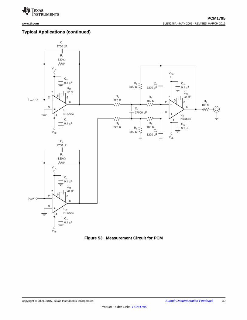
–
+
R
8201
W
2
3
75
8
6
4
C
0.1 F11
m
C
22 pF17
VCC
C
2700 pF1
C12
0.1 Fm
VEE
U
NE55341
I -OUT
R2
820 W
2
3
75
8
6
4
C13
0.1 Fm
C18
22 pF
VCC
C2
2700 pF
C14
0.1 Fm
VEE
U2
NE5534
I +OUT
–
+
2
3
7
4
C15
0.1 Fm
VCC
C16
0.1 Fm
VEE
U3
NE5534
R9
100 W
C3
8200 pF
R
2005
W
C4
8200 pF
R6
200 W
R
2203
W
R4
220 W
C
27000 pF5
R7
180 W
R8
180 W
58
6
C19
22 pF
–
+
PCM1795www.ti.com SLES248A –MAY 2009–REVISED MARCH 2015
Typical Applications (continued)
Figure 53. Measurement Circuit for PCM
Copyright © 2009–2015, Texas Instruments Incorporated Submit Documentation Feedback 39
Product Folder Links: PCM1795
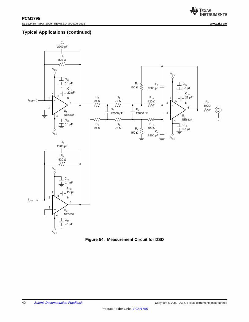
–
+
R
8201
W
2
3
75
8
6
4
C
0.1 F11
m
C
22 pF17
VCC
C
2200 pF1
C12
0.1 Fm
VEE
U
NE55341
I -OUT
R2
820 W
2
3
75
8
6
4
C13
0.1 Fm
C18
22 pF
VCC
C2
2200 pF
C14
0.1 Fm
VEE
U2
NE5534
I +OUT
–
+
2
3
7
4
C15
0.1 Fm
VCC
C16
0.1 Fm
VEE
U3
NE5534
R7
100W
C5
8200 pF
R
1505
W
C6
8200 pF
R6
150 W
R
758
W
R9
75 W
C
27000 pF4
R10
120 W
R11
120 W
58
6
C19
22 pF
–
+
R
913
W
R4
91 W
C
22000 pF3
PCM1795SLES248A –MAY 2009–REVISED MARCH 2015 www.ti.com
Typical Applications (continued)
Figure 54. Measurement Circuit for DSD
40 Submit Documentation Feedback Copyright © 2009–2015, Texas Instruments Incorporated
Product Folder Links: PCM1795

0.0005
0.0004
0.0003
0.0002
0.0001
0
0.0001
0.0002
0.0003
0.0004
0.0005
-
-
-
-
-
Am
plit
ude (
dB
)
Frequency ( f )´ S
0 0.2 0.50.1 0.3 0.4
Passband Ripple
Sharp Roll-Off
0
2
4
6
8
10
12
14
16
18
20
-
-
-
-
-
-
-
-
-
-
Am
plit
ude (
dB
)
Frequency ( f )´ S
0 0.2 0.60.1 0.3 0.4 0.5
Transition Characteristics
Slow Roll-Off
IOUT-
Circuit(1)
IOUTL (Pin 26)-
OUT+
1
2
3
Balanced Out
OUT-
IOUTL+ (Pin 25)
IOUTR+ (Pin 17)
IOUTR (Pin 18)- IOUT-
I +OUT
I +OUT
Circuit(1)
PCM1795www.ti.com SLES248A –MAY 2009–REVISED MARCH 2015
Typical Applications (continued)
(1) Circuit corresponds to Figure 53.
Figure 55. Measurement Circuit for Monaural Mode
8.2.1.3 Application Curves
Figure 56. Amplitude vs Frequency Figure 57. Amplitude vs Frequency
Copyright © 2009–2015, Texas Instruments Incorporated Submit Documentation Feedback 41
Product Folder Links: PCM1795
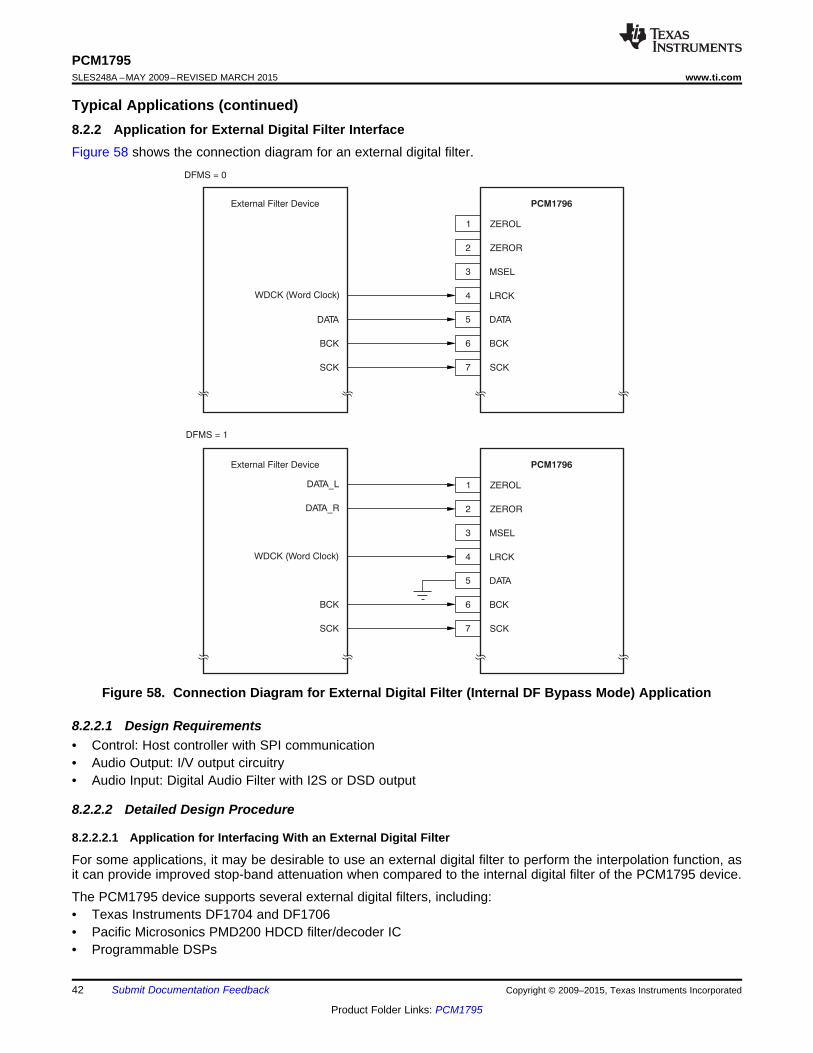
DATA
BCK
SCK
WDCK (Word Clock)
External Filter Device
DATA5
6
7
BCK
SCK
ZEROL1
2
3
4
ZEROR
MSEL
LRCK
PCM1796
DFMS = 0
BCK
SCK
WDCK (Word Clock)
External Filter Device
DATA
BCK
SCK
ZEROL
5
6
7
1
2
3
4
ZEROR
MSEL
LRCK
PCM1796
DFMS = 1
DATA_L
DATA_R
PCM1795SLES248A –MAY 2009–REVISED MARCH 2015 www.ti.com
Typical Applications (continued)8.2.2 Application for External Digital Filter InterfaceFigure 58 shows the connection diagram for an external digital filter.
Figure 58. Connection Diagram for External Digital Filter (Internal DF Bypass Mode) Application
8.2.2.1 Design Requirements• Control: Host controller with SPI communication• Audio Output: I/V output circuitry• Audio Input: Digital Audio Filter with I2S or DSD output
8.2.2.2 Detailed Design Procedure
8.2.2.2.1 Application for Interfacing With an External Digital Filter
For some applications, it may be desirable to use an external digital filter to perform the interpolation function, asit can provide improved stop-band attenuation when compared to the internal digital filter of the PCM1795 device.
The PCM1795 device supports several external digital filters, including:• Texas Instruments DF1704 and DF1706• Pacific Microsonics PMD200 HDCD filter/decoder IC• Programmable DSPs
42 Submit Documentation Feedback Copyright © 2009–2015, Texas Instruments Incorporated
Product Folder Links: PCM1795

MSB
16
BCK
DATA,DATAL, DATAR
1/4 fS or 1/8 fS
WDCK
Audio Data Word = 16-Bit
Audio Data Word = 32-Bit
Audio Data Word = 24-Bit
1 2 3 4 5 6 7 8 9 10 11 12 13 14 151615
LSB
2819 20 21 22 23 24 25 26 273231 3229 30 31
161 2 3 4 5 6 7 8 9 10 11 12 13 14 152423 2017 18 19 2421 22 23
DATA,DATAL, DATAR
DATA,DATAL, DATAR
MSB LSB
MSB LSB
1 2 3 4 5
PCM1795www.ti.com SLES248A –MAY 2009–REVISED MARCH 2015
Typical Applications (continued)The external digital filter application mode is accessed by programming the following bits in the correspondingcontrol register:• DFTH = 1 (register 20)
The pins used to provide the serial interface for the external digital filter are illustrated in Figure 58. The wordclock (WDCK) signal must be operated at 8 times or 4 times the desired sampling frequency, fS.
8.2.2.2.2 Pin Assignment When Using the External Digital Filter Interface• LRCK (pin 4): WDCK as word clock input• BCK (pin 6): Bit clock for audio data• DATA (pin 5): Monaural audio data input when the DFMS bit is not set to 1• ZEROL (pin 1): DATAL as left channel audio data input when the DFMS bit is set to 1• ZEROR (pin 2): DATAR as right channel audio data input when the DFMS bit is set to 1
8.2.2.2.3 Audio Format
The PCM1795 device in the external digital filter interface mode supports right-justified audio formats including16-bit, 24-bit, and 32-bit audio data, as shown in Figure 59. The audio format is selected by the FMT[2:0] bits ofcontrol register 18.
Figure 59. Audio Data Input Format for External Digital Filter (Internal DF Bypass Mode) Application
8.2.2.2.4 System Clock (SCK) and Interface Timing
The PCM1795 device in an application using an external digital filter requires the synchronization of WDCK andthe system clock. The system clock is phase-free with respect to WDCK. Interface timing among WDCK, BCK,DATA, DATAL, and DATAR is shown in Figure 60 and Table 32.
Copyright © 2009–2015, Texas Instruments Incorporated Submit Documentation Feedback 43
Product Folder Links: PCM1795

t(BCH)
BCK
WDCK
t(BCL) t(LB)
t(BCY)
t(DS) t(DH)
1.4 V
1.4 V
t(BL)
1.4 V
DATA
DATAL
DATAR
PCM1795SLES248A –MAY 2009–REVISED MARCH 2015 www.ti.com
Typical Applications (continued)
Figure 60. Audio Interface Timing for External Digital Filter (Internal DF Bypass Mode) Application
Table 32. Timing Characteristics for Figure 60MIN MAX UNIT
t(BCY) BCK pulse cycle time 20 nst(BCL) BCK pulse duration, low 7 nst(BCH) BCK pulse duration, high 7 nst(BL) BCK rising edge to WDCK falling edge 5 nst(LB) WDCK falling edge to BCK rising edge 5 nst(DS) DATA, DATAL, DATAR setup time 5 nst(DH) DATA, DATAL, DATAR hold time 5 ns
8.2.2.2.5 Functions Available in the External Digital Filter Mode
The external digital filter mode is selected by setting DSD = 0 (register 20, B5) and DFTH = 1 (register 20, B4).
The external digital filter mode allows access to the majority of the PCM1795 mode control functions.
Table 33 shows the register mapping available when the external digital filter mode is selected, along withdescriptions of functions that are modified when using this mode selection.
Table 33. External Digital Filter Register MapREGISTER B15 B14 B13 B12 B11 B10 B9 B8 B7 B6 B5 B4 B3 B2 B1 B0
Register 16 R/W 0 0 1 0 0 0 0 X (1) X X X X X X X
Register 17 R/W 0 0 1 0 0 0 1 X X X X X X X X
Register 18 R/W 0 0 1 0 0 1 0 X FMT2 FMT1 FMT0 X X X X
Register 19 R/W 0 0 1 0 0 1 1 REV X X OPE X DFMS X INZD
Register 20 R/W 0 0 1 0 1 0 0 X SRST 0 1 MONO CHSL OS1 OS0
Register 21 R/W 0 0 1 0 1 0 1 X X X X X X X PCMZ
Register 22 R 0 0 1 0 1 1 0 X X X X X X ZFGR ZFGL
(1) Function is disabled. No operation even if data bit is set.
44 Submit Documentation Feedback Copyright © 2009–2015, Texas Instruments Incorporated
Product Folder Links: PCM1795

0.0005
0.0004
0.0003
0.0002
0.0001
0
0.0001
0.0002
0.0003
0.0004
0.0005
-
-
-
-
-
Am
plit
ude (
dB
)
Frequency ( f )´ S
0 0.2 0.50.1 0.3 0.4
Passband Ripple
Sharp Roll-Off
0
2
4
6
8
10
12
14
16
18
20
-
-
-
-
-
-
-
-
-
-
Am
plit
ude (
dB
)
Frequency ( f )´ S
0 0.2 0.60.1 0.3 0.4 0.5
Transition Characteristics
Slow Roll-Off
PCM1795www.ti.com SLES248A –MAY 2009–REVISED MARCH 2015
8.2.2.2.5.1 FMT[2:0]: Audio Data Format Selection
Default value: 000
Table 34. FMT[2:0]FMT[2:0] AUDIO DATA FORMAT SELECTION
000 16-bit right-justified format001 32-bit right-justified format010 24-bit right-justified format (default)
Other N/A
8.2.2.2.5.2 OS[1:0]: ΔΣ Modulator Oversampling Rate Selection
Default value: 00
Table 35. OS[1:0]OS[1:0] OPERATION SPEED SELECTION
00 8 times WDCK (default)01 4 times WDCK10 16 times WDCK11 Reserved
The effective oversampling rate is determined by the oversampling performed by both the external digital filterand the ΔΣ modulator. For example, if the external digital filter is 8× oversampling, and OS[1:0] = 00 is selected,then the ΔΣ modulator oversamples by 8×, resulting in an effective oversampling rate of 64×. The 16× WDCKoversampling rate is not available above a 100-kHz sampling rate. If the oversampling rate selected is 16×WDCK, the system clock frequency must be over 256 fS.
8.2.2.3 Application Curves
Figure 61. Amplitude vs Frequency Figure 62. Amplitude vs Frequency
Copyright © 2009–2015, Texas Instruments Incorporated Submit Documentation Feedback 45
Product Folder Links: PCM1795

Bit Clock
DSD Decoder
DATA
BCK
SCK
ZEROL
5
6
7
1
2
3
4
ZEROR
MSEL
LRCK
PCM1796
DATA_L
DATA_R
PCM1795SLES248A –MAY 2009–REVISED MARCH 2015 www.ti.com
8.2.3 Application for DSD Format (DSD Mode) InterfaceFigure 63 shows a connection diagram for DSD mode.
Figure 63. Connection Diagram in DSD Mode
8.2.3.1 Design Requirements• Control: Host controller with SPI communication• Audio Output: I/V output circuitry• Audio Input: DSD Digital Audio input
8.2.3.2 Detailed Design Procedure
8.2.3.2.1 Features
This mode is used for interfacing directly to a DSD decoder, which is found in Super Audio CD™ (SACD)applications.
The DSD mode is accessed by programming the following bit in the corresponding control register.• DSD = 1 (register 20)
The DSD mode provides a low-pass filtering function. The filtering is provided using an analog FIR filter structure.Four FIR responses are available and are selected by the DMF[1:0] bits of control register 18.
The DSD bit must be set before inputting DSD data; otherwise, the PCM1795 erroneously detects the TDMCAmode and commands are not accepted through the serial control interface.
8.2.3.2.2 Pin Assignment When Using DSD Format Interface
Several pins are redefined for DSD mode operation. These include:• DATA (pin 5): DSDL as left-channel DSD data input• LRCK (pin 4): DSDR as right-channel DSD data input• SCK (pin 7): DBCK as bit clock for DSD data• BCK (pin 6): Set low (N/A)
8.2.3.2.3 Requirements for System Clock
For operation in DSD mode, the bit clock (DBCK) is required on pin 7 of the PCM1795. The frequency of the bitclock can be N times the sampling frequency. Generally, N is 64 in DSD applications.
The interface timing between the bit clock and DSDL and DSDR is required to meet the setup and hold timespecifications shown in Figure 65 and Table 36.
46 Submit Documentation Feedback Copyright © 2009–2015, Texas Instruments Incorporated
Product Folder Links: PCM1795

DSDL,
DSDR
t(BCH)
DBCK
t(BCL)
t(BCY)
1.4 V
1.4 V
t(DS) t(DH)
t = 1/(64 44.1 kHz)´
D1DSDL,
DSDRD0 D2 D3 D4
DBCK
PCM1795www.ti.com SLES248A –MAY 2009–REVISED MARCH 2015
Figure 64. Normal Data Output Form From DSD Decoder
Figure 65. Timing for DSD Audio Interface
Table 36. Timing Characteristics for Figure 65MIN MAX UNIT
t(BCY) DBCK pulse cycle time 85 (1) nst(BCH) DBCK high-level time 30 nst(BCL) DBCK low-level time 30 nst(DS) DSDL, DSDR setup time 10 nst(DH) DSDL, DSDR hold time 10 ns
(1) 2.8224 MHz × 4. (2.8224 MHz = 64 × 44.1 kHz. This value is specified as a sampling rate of DSD.
8.2.3.2.4 DSD Mode Configuration and Function Controls
8.2.3.2.4.1 Configuration for the DSD Interface Mode
The DSD interface mode is selected by setting DSD = 1 (register 20, B5).
Table 37. DSD Mode Register MapREGISTER B15 B14 B13 B12 B11 B10 B9 B8 B7 B6 B5 B4 B3 B2 B1 B0
Register 16 R/W 0 0 1 0 0 0 0 X (1) X X X X X X X
Register 17 R/W 0 0 1 0 0 0 1 X X X X X X X X
Register 18 R/W 0 0 1 0 0 1 0 X X X X DMF1 DMF0 X X
Register 19 R/W 0 0 1 0 0 1 1 REV X X OPE X X X X
Register 20 R/W 0 0 1 0 1 0 0 X SRST 1 X MONO CHSL OS1 OS0
Register 21 R 0 0 1 0 1 0 1 X X X X X DZ1 DZ0 X
Register 22 R 0 0 1 0 1 1 0 X X X X X X ZFGR ZFGL
(1) Function is disabled. No operation even if data bit is set.
Copyright © 2009–2015, Texas Instruments Incorporated Submit Documentation Feedback 47
Product Folder Links: PCM1795

0.0005
0.0004
0.0003
0.0002
0.0001
0
0.0001
0.0002
0.0003
0.0004
0.0005
-
-
-
-
-
Am
plit
ude (
dB
)
Frequency ( f )´ S
0 0.2 0.50.1 0.3 0.4
Passband Ripple
Sharp Roll-Off
0
2
4
6
8
10
12
14
16
18
20
-
-
-
-
-
-
-
-
-
-
Am
plit
ude (
dB
)
Frequency ( f )´ S
0 0.2 0.60.1 0.3 0.4 0.5
Transition Characteristics
Slow Roll-Off
PCM1795SLES248A –MAY 2009–REVISED MARCH 2015 www.ti.com
8.2.3.2.4.2 DMF[1:0]: Analog-FIR Performance Selection
Default value: 00
Table 38. DMF[1:0]DMF[1:0] ANALOG-FIR PERFORMANCE SELECTION
00 FIR-1 (default)01 FIR-210 FIR-311 FIR-4
Plots for the four analog finite impulse response (FIR) filter responses are shown in Analog FIR FilterPerformance in DSD Mode .
8.2.3.2.4.3 OS[1:0]: Analog-FIR Operation-Speed Selection
Default value: 00
Table 39. OS[1:0]OS[1:0] OPERATING SPEED SELECTION
00 fDBCK (default)01 fDBCK/210 Reserved11 fDBCK/4
The OS bit in the DSD mode is used to select the operating rate of the analog FIR. The OS bits must be setbefore setting the DSD bit to '1'.
8.2.3.3 Application Curves
Figure 66. Amplitude vs Frequency Figure 67. Amplitude vs Frequency
48 Submit Documentation Feedback Copyright © 2009–2015, Texas Instruments Incorporated
Product Folder Links: PCM1795

Pre-TDMCA Frame
BCK
LRCK
TDMCA FrameCommand
Accept
2 BCKs
FSX
FSR
CLKX
DX
CLKR
DR
TI DSP
Host
Controller
IN Device
PCM1795
LRCK
BCK
DI
DO
DCI
VDD
Device ID = 1
DCO
PCM1795www.ti.com SLES248A –MAY 2009–REVISED MARCH 2015
8.2.4 TDMCA Interface FormatThe PCM1795 device supports the time-division-multiplexed command and audio (TDMCA) data format tosimplify the host control serial interface. TDMCA format is designed not only for the multichannel buffered serialport description (McBSP) of TI DSPs but also for any programmable devices. TDMCA format can transfer notonly audio data but also command data, so that it can be used together with any kind of device that supportsTDMCA format. The TDMCA frame consists of a command field, extended command field, and some audio datafields. Those audio data are transported to IN devices (such as a DAC) and/or from OUT devices (such as anADC). The PCM1795 is an IN device. LRCK and BCK are used with both IN and OUT devices so that thesample frequency of all devices in a system must be the same. The TDMCA mode supports a maximum of 30device IDs. The maximum number of audio channels depends on the BCK frequency.
Figure 68. TDMCA Diagram
8.2.4.1 Design Requirements• Control: TDMCA control information• Audio Input: TDMCA input with LRCK signal with a pulse of two BCK clocks• Audio Output: I/V output circuitry
8.2.4.2 Detailed Design Procedure
8.2.4.2.1 TDMCA Mode Determination
The PCM1795 device recognizes the TDMCA mode automatically when it receives an LRCK signal with a pulseduration of two BCK clocks. If the TDMCA mode operation is not needed, the duty cycle of LRCK must be 50%.Figure 69 shows the LRCK and BCK timing that determines the TDMCA mode. The PCM1795 device entersTDMCA mode after two continuous TDMCA frames. Any TDMCA commands can be issued during the nextTDMCA frame after entering TDMCA mode.
Figure 69. LRCK and BCK Timing for Determination of TDMCA Mode
8.2.4.2.2 TDMCA Terminals
TDMCA requires six signals: four signals are for the command and audio data interface, and one pair for daisy-chaining. These signals can be shared as shown in Table 40. The DO signal has a 3-state output so that it canbe connected directly to other devices.
Copyright © 2009–2015, Texas Instruments Incorporated Submit Documentation Feedback 49
Product Folder Links: PCM1795

IN Device
DC
I
DC
O
OUT Device
DC
I
DC
O
IN
OUT
IN/OUT
Device
IN Chain
OUT Chain
IN Device
OUT Device
DC
I
DC
O
DC
I
DC
O
DC
IiD
CIo
DC
Oi
DC
Oo
IN
OUT
DC
IiD
CIo
DC
Oi
DC
Oo
NO Device
DC
I
DC
O
NO Device
DC
I
DC
O
NO Device
NO Device
DC
I
DC
O
DC
I
DC
OIN/OUT
Device
¼
¼
¼
¼
¼
PCM1795SLES248A –MAY 2009–REVISED MARCH 2015 www.ti.com
Table 40. TDMCA TerminalsTERMINAL NAME TDMCA NAME PROPERTY DESCRIPTION
TDMCA frame start signal; it must be the same as the samplingLRCK LRCK Input frequencyTDMCA clock; its frequency must be high enough to communicate aBCK BCK Input TDMCA frame within an LRCK cycle
DATA DI Input TDMCA command and audio data input signalMDO DO Output TDMCA command data 3-state output signalMC DCI Input TDMCA daisy-chain input signalMS DCO Output TDMCA daisy-chain output signal
8.2.4.2.3 Device ID Determination
TDMCA mode also supports a multichip implementation in one system. This capability means that a hostcontroller (DSP) can simultaneously support several TDMCA devices, which can be of the same type or differenttypes, including PCM devices. The PCM devices are categorized as either IN devices, OUT devices, IN/OUTdevices, and NO devices. The IN device has an input port to receive audio data; the OUT device has an outputport to supply audio data; the IN/OUT device has both input and output ports for audio data; and the NO devicehas no port for audio data, but requires command data from the host. A DAC is an IN device; an ADC is an OUTdevice; a codec is an IN/OUT device; and a PLL is a NO device. The PCM1795 is an IN device. For the hostcontroller to distinguish the devices, each device is assigned its own device ID by the daisy-chain. The devicesobtain their own device IDs automatically by connecting the DCI to the DCO of the preceding device and theDCO to the DCI of the following device in the daisy-chain. The daisy-chains are categorized as the IN chain andthe OUT chain, which are completely independent and equivalent. Figure 70 shows an example daisy-chainconnection. If a system must chain the PCM1795 device and a NO device in the same IN or OUT chain, the NOdevice must be chained at the back end of the chain because it does not require any audio data. Figure 71shows an example TDMCA system including an IN chain and an OUT chain with a TI DSP. For a device to getits own device ID, the DID signal must be set to '1' (see the Command Field section for details), and LRCK andBCK must be driven in the TDMCA mode for all PCM devices that are chained. The device at the top of the chainknows its device ID is '1' because its DCI is fixed high. Other devices count the BCK pulses and observe therespective DCI signal to determine ID and position in the chain. Figure 72 shows the initialization of each deviceID.
Figure 70. Daisy-Chain Connection Example
50 Submit Documentation Feedback Copyright © 2009–2015, Texas Instruments Incorporated
Product Folder Links: PCM1795

IN Device
( )PCM1795
DCI
DCO
LRCK
BCK
DI
DODevice ID = 2
TI DSP
FSX
CLKX
DX
FSR
CLKR
DR
NO DeviceDCI
DCO
OUT DeviceDCI
DCO
OUT DeviceDCI
DCO
Device ID = 3
Device ID = 2
Device ID = 3
LRCK
BCK
DI
DO
LRCK
BCK
DI
DO
LRCK
BCK
DI
DO
IN/OUT
Device
( )DIX1700
DCII
DCIO
LRCK
BCK
DI
DO
Device ID = 1
DCOO
DCOI
¼¼
PCM1795www.ti.com SLES248A –MAY 2009–REVISED MARCH 2015
Figure 71. IN Daisy-Chain and OUT Daisy-Chain Connection Example for a Multichip System
Copyright © 2009–2015, Texas Instruments Incorporated Submit Documentation Feedback 51
Product Folder Links: PCM1795

LRCK
BCK
DI CMD EMD EMD EMD CMDDon’t
CareEMD EMD
DO Ch 1 Ch (m)Ch 2CMD
CMD Ch 2 Ch 3 Ch (n) CMDCh 1 Ch 4DI
Ch 3 Ch 4
[For Initialization]
[For Operation]
32 Bits
DO CMD CMD CMD CMD CMD CMD
1/fS
Don’t
Care
58 BCKs
Command FieldDID
LRCK
BCK
DI
DCO1,
DCI2
Device ID = 1
Device ID = 2
DCO1
DCO2,
DCI3
DCO29,
DCI30
Device ID = 3
Device ID = 30
PCM1795SLES248A –MAY 2009–REVISED MARCH 2015 www.ti.com
Figure 72. Device ID Determination Sequence
8.2.4.2.4 TDMCA Frame
In general, the TDMCA frame consists of the command field, extended command (EMD) field, and audio datafields. All fields are 32 bits long, but the lowest byte has no meaning. The MSB is transferred first for each field.The command field is always transferred as the first packet of the frame. The EMD field is transferred if the EMDflag of the command field is high. If any EMD packets are transferred, no audio data follow the EMD packets.This frame is for quick system initialization. All devices of a daisy-chain should respond to the command field andextended command field. The PCM1795 has two audio channels that can be selected by OPE (register 19). Ifthe OPE bit is not set to high, those audio channels are transferred. Figure 73 shows the general TDMCA frame.If some DACs are enabled, but corresponding audio data packets are not transferred, the analog outputs areunpredictable.
Figure 73. General TDMCA Frame
52 Submit Documentation Feedback Copyright © 2009–2015, Texas Instruments Incorporated
Product Folder Links: PCM1795

31
Command
30 29 2328 24 22 15 716 8 0
DID EMD DCS R/WDevice ID Register ID Data Not Used
LRCK
BCK
DIDon’t
Care
Ch 1
Ch 2 Ch 3Ch 1 Ch 4
IN and OUT Channel Orders are Completely Independent
DO
7 Packets 32 Bits´
Ch 5 Ch 6
1/f (256 BCK Clocks)S
Ch 2
CMDCMD
CMD
PCM1795www.ti.com SLES248A –MAY 2009–REVISED MARCH 2015
Figure 74. TDMCA Frame Example of Six-Channel DAC and Two-Channel ADC With Command Read
8.2.4.2.5 Command Field
The normal command field is defined as shown in Figure 75. When the DID bit (MSB) is '1', this frame is usedonly for device ID determination, and all remaining bits in the field are ignored.
Figure 75. Normal Command Field
8.2.4.2.5.1 Bit 31: Device ID Enable Flag
The PCM1795 operates to get its own device ID for TDMCA initialization if this bit is high.
8.2.4.2.5.2 Bit 30: Extended Command Enable Flag
The EMD packet is transferred if this bit is high; otherwise, it is skipped. Once this bit is high, this frame does notcontain any audio data. This is for system initialization.
8.2.4.2.5.3 Bit 29: Daisy-Chain Selection Flag
A high setting designates OUT-chain devices, low designates IN-chain devices. The PCM1795 is an IN device,so the DCS bit must be set low.
8.2.4.2.5.4 Bits[28:24]: Device ID
The device ID is 5 bits long and it can be defined. These bits identify the order of a device in the IN or OUTdaisy-chain. The top of the daisy-chain defines device ID 1 and successive devices are numbered 2, 3, 4, etc. Alldevices for which the DCI is fixed high are also defined as ID 1. The maximum device ID is 30 each in the IN andOUT chains. If a device ID of 0x1F is used, all devices are selected as broadcast when in the write mode. If adevice ID of 0x00 is used, no device is selected.
8.2.4.2.5.5 Bit 23: Command Read/Write flag
If this bit is high, the command is a read operation.
8.2.4.2.5.6 Bits[22:16]: Register ID
The register ID is 7 bits long.
8.2.4.2.5.7 Bits[15:8]: Command data
The command data are 8 bits long. Any valid data can be chosen for each register.
8.2.4.2.5.8 Bits[7:0]: Not used
These bits are never transported when a read operation is performed.
Copyright © 2009–2015, Texas Instruments Incorporated Submit Documentation Feedback 53
Product Folder Links: PCM1795

BCK
DI
DO
DOEN
(Internal)
1 BCK Early
Read Mode and Proper Register ID Write Data Retrieved, if Write Mode
Read Data Driven, if Read Mode
Register ID Phase Data Phase
31
Audio Data
12 716 8 0
MSB 24 Bits LSB All 0s
4 3
31
Extended Command
30 29 2328 24 22 15 716 8 0
RSVD EMD DCS R/WDevice ID Register ID Data Not Used
PCM1795SLES248A –MAY 2009–REVISED MARCH 2015 www.ti.com
8.2.4.2.6 Extended Command Field
The extended command field is the same as the command field, except that it does not have a DID flag.Figure 76 defines the extended command field.
Figure 76. Extended Command Field
8.2.4.2.7 Audio Fields
The audio field is 32 bits long and the audio data are transferred MSB first, so the other fields must be filled with0s as shown in Figure 77.
Figure 77. Audio Field Example
8.2.4.2.8 TDMCA Register Requirements
The TDMCA mode requires device ID and audio channel information, as previously described. The OPE bit inregister 19 indicates audio channel availability and register 23 indicates the device ID. Register 23 is used only inthe TDMCA mode; see the mode control register map of Table 10.
8.2.4.2.9 Register Write/Read Operation
The command supports register write and read operations. If the command requests to read one register, theread data are transferred on DO during the data phase of the timing cycle. The DI signal can be retrieved at thepositive edge of BCK, and the DO signal is driven at the negative edge of BCK. DO is activated one BCK cycleearly to compensate for the output delay caused by high impedance. Figure 78 shows the TDMCA write andread timing.
Figure 78. TDMCA Write and Read Operation Timing
54 Submit Documentation Feedback Copyright © 2009–2015, Texas Instruments Incorporated
Product Folder Links: PCM1795
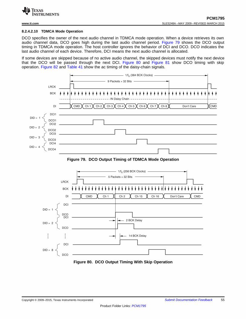
14 BCK Delay
2 BCK Delay
DID = 1
DID = 2
DID = 8
Don’t CareCMD CMDCh 2 Ch 15
5 Packets 32 Bits´
1/f (256 BCK Clocks)S
DCI
DCO
DCO
DI
¼¼Ch 1 Ch 16
DCI
DCO
DCI
LRCK
BCK
9 Packets ´ 32 Bits
LRCK
BCK
DI Don’t Care
DCI1
DCO1DID = 1
DCI2
DCO2DID = 2
DCI3
DCO3DID = 3
DCI4
DCO4DID = 4
CMD
1/fS (384 BCK Clocks)
CMD Ch 1 Ch 2 Ch 3 Ch 4 Ch 5 Ch 6 Ch 7 Ch 8
IN Daisy Chain
PCM1795www.ti.com SLES248A –MAY 2009–REVISED MARCH 2015
8.2.4.2.10 TDMCA Mode Operation
DCO specifies the owner of the next audio channel in TDMCA mode operation. When a device retrieves its ownaudio channel data, DCO goes high during the last audio channel period. Figure 79 shows the DCO outputtiming in TDMCA mode operation. The host controller ignores the behavior of DCI and DCO. DCO indicates thelast audio channel of each device. Therefore, DCI means the next audio channel is allocated.
If some devices are skipped because of no active audio channel, the skipped devices must notify the next devicethat the DCO will be passed through the next DCI. Figure 80 and Figure 81 show DCO timing with skipoperation. Figure 82 and Table 41 show the ac timing of the daisy-chain signals.
Figure 79. DCO Output Timing of TDMCA Mode Operation
Figure 80. DCO Output Timing With Skip Operation
Copyright © 2009–2015, Texas Instruments Incorporated Submit Documentation Feedback 55
Product Folder Links: PCM1795

t(COE)
BCK
LRCK
DI
DCI
DO
DCO
t(DS)
t(BL)t(LB)
t(BCY) t(DS)
t(DOE)
t(DH)
t(DH)
Command Packet
LRCK
BCK
DI
DCO1
DCO2
DID EMD
¼
PCM1795SLES248A –MAY 2009–REVISED MARCH 2015 www.ti.com
Figure 81. DCO Output Timing With Skip Operation (for Command Packet 1)
Figure 82. AC Timing of Daisy-Chain Signals
Table 41. Timing Characteristics for Figure 82MIN MAX UNIT
t(BCY) BCK pulse cycle time 20 nst(LB) LRCK setup time 0 nst(BL) LRCK hold time 3 nst(DS) DI setup time 0 nst(DH) DI hold time 3 nst(DS) DCI setup time 0 nst(DH) DCI hold time 3 nst(DOE) DO output delay (1) 8 nst(COE) DCO output delay (1) 6 ns
(1) Load capacitance is 10 pF.
56 Submit Documentation Feedback Copyright © 2009–2015, Texas Instruments Incorporated
Product Folder Links: PCM1795

PCM1795www.ti.com SLES248A –MAY 2009–REVISED MARCH 2015
9 Power Supply RecommendationsThe PCM1795 device requires a 5-V nominal supply and a 3.3-V nominal supply. The 5-V supply is for theanalog circuitry powered by VCC1, VCC2L, and VCC2R pins. The 3.3-V supply is for the digital circuitry powered bythe VDD pin. The decoupling capacitors for the power supplies should be placed close to the device terminals.
10 Layout
10.1 Layout GuidelinesDesigners should try to use the same ground between AGND and DGND to avoid any potential voltagedifference between them. Ensure that the return currents for digital signals will avoid the AGND pin or the inputsignals to the I/V stage. Avoid running high-frequency clock and control signals near AGND, or any of the VOUTpins where possible. The pin layout of the PCM1795 device partitions into two sides, the analog side and thedigital side. Providing the system is partitioned in such a way that digital signals are routed away from the analogsections, then no digital return currents (for example, clocks) should be generated in the analog circuitry.• Decoupling capacitors should be placed as close to the VCC1, VCC2L, VCCR2, VCOML, VCOMR, and VDD pins as
possible.• Further guidelines can be found in Figure 83.
Copyright © 2009–2015, Texas Instruments Incorporated Submit Documentation Feedback 57
Product Folder Links: PCM1795

3
4
5
6
7
8
9
28
27
26
25
24
23
22
21
20
19
18
17
16
15
0.1 µF10 µF
+3.3V
0.1 µF 10 µF
+
10 µF
+
0.1 µF 10 µF
+
5V
5V
5V
47 µF+
10 KO
Left I/V
Output
circuit
Right I/V
Output
circuit
It is recommended to place a top layer ground pour for
shielding around PCM1795 and connect to lower main PCB
ground plane by multiple vias
These resistors help prevent
overshoot and reduce
coupling, Start at 10? for
MCLK and 27? for others.
ZeroL
ZeroR
MSEL
LRCK
DATA
BCK
SCK
DGND
VDD
MS
MDI
MC
RST
MDO
VCC2L
AGND3L
IoutL-
IoutL+
AGND2
Iref
VCC1
VcomL
VcomR
AGND1
IoutR-
IoutR+
VCC2R
AGND3R
PCM1795
10
11
13
14
12Communication
signals to host
1
2
Signals to host
Top Layer Ground Pour
Top Layer Signal Traces
Via to bottom Ground Plane
Pad to top layer ground pour
Ω
Ω
PCM1795SLES248A –MAY 2009–REVISED MARCH 2015 www.ti.com
10.2 Layout Example
Figure 83. Layout Recommendation
58 Submit Documentation Feedback Copyright © 2009–2015, Texas Instruments Incorporated
Product Folder Links: PCM1795

PCM1795www.ti.com SLES248A –MAY 2009–REVISED MARCH 2015
11 Device and Documentation Support
11.1 Device Support
11.1.1 Third-Party Products DisclaimerTI'S PUBLICATION OF INFORMATION REGARDING THIRD-PARTY PRODUCTS OR SERVICES DOES NOTCONSTITUTE AN ENDORSEMENT REGARDING THE SUITABILITY OF SUCH PRODUCTS OR SERVICESOR A WARRANTY, REPRESENTATION OR ENDORSEMENT OF SUCH PRODUCTS OR SERVICES, EITHERALONE OR IN COMBINATION WITH ANY TI PRODUCT OR SERVICE.
11.2 TrademarksSystem Two, Audio Precision are trademarks of Audio Precision, Inc.SPI is a trademark of Motorola.Pacific Microsonics is a trademark of Pacific Microsonics, Inc.Super Audio CD is a trademark of Sony Corporation.All other trademarks are the property of their respective owners.
11.3 Electrostatic Discharge CautionThese devices have limited built-in ESD protection. The leads should be shorted together or the device placed in conductive foamduring storage or handling to prevent electrostatic damage to the MOS gates.
11.4 GlossarySLYZ022 — TI Glossary.
This glossary lists and explains terms, acronyms, and definitions.
12 Mechanical, Packaging, and Orderable InformationThe following pages include mechanical, packaging, and orderable information. This information is the mostcurrent data available for the designated devices. This data is subject to change without notice and revision ofthis document. For browser-based versions of this data sheet, refer to the left-hand navigation.
Copyright © 2009–2015, Texas Instruments Incorporated Submit Documentation Feedback 59
Product Folder Links: PCM1795

PACKAGE OPTION ADDENDUM
www.ti.com 2-Oct-2014
Addendum-Page 1
PACKAGING INFORMATION
Orderable Device Status(1)
Package Type PackageDrawing
Pins PackageQty
Eco Plan(2)
Lead/Ball Finish(6)
MSL Peak Temp(3)
Op Temp (°C) Device Marking(4/5)
Samples
PCM1795DB ACTIVE SSOP DB 28 50 Green (RoHS& no Sb/Br)
CU NIPDAU Level-1-260C-UNLIM -25 to 85 PCM1795
PCM1795DBR ACTIVE SSOP DB 28 2000 Green (RoHS& no Sb/Br)
CU NIPDAU Level-1-260C-UNLIM -25 to 85 PCM1795
(1) The marketing status values are defined as follows:ACTIVE: Product device recommended for new designs.LIFEBUY: TI has announced that the device will be discontinued, and a lifetime-buy period is in effect.NRND: Not recommended for new designs. Device is in production to support existing customers, but TI does not recommend using this part in a new design.PREVIEW: Device has been announced but is not in production. Samples may or may not be available.OBSOLETE: TI has discontinued the production of the device.
(2) Eco Plan - The planned eco-friendly classification: Pb-Free (RoHS), Pb-Free (RoHS Exempt), or Green (RoHS & no Sb/Br) - please check http://www.ti.com/productcontent for the latest availabilityinformation and additional product content details.TBD: The Pb-Free/Green conversion plan has not been defined.Pb-Free (RoHS): TI's terms "Lead-Free" or "Pb-Free" mean semiconductor products that are compatible with the current RoHS requirements for all 6 substances, including the requirement thatlead not exceed 0.1% by weight in homogeneous materials. Where designed to be soldered at high temperatures, TI Pb-Free products are suitable for use in specified lead-free processes.Pb-Free (RoHS Exempt): This component has a RoHS exemption for either 1) lead-based flip-chip solder bumps used between the die and package, or 2) lead-based die adhesive used betweenthe die and leadframe. The component is otherwise considered Pb-Free (RoHS compatible) as defined above.Green (RoHS & no Sb/Br): TI defines "Green" to mean Pb-Free (RoHS compatible), and free of Bromine (Br) and Antimony (Sb) based flame retardants (Br or Sb do not exceed 0.1% by weightin homogeneous material)
(3) MSL, Peak Temp. - The Moisture Sensitivity Level rating according to the JEDEC industry standard classifications, and peak solder temperature.
(4) There may be additional marking, which relates to the logo, the lot trace code information, or the environmental category on the device.
(5) Multiple Device Markings will be inside parentheses. Only one Device Marking contained in parentheses and separated by a "~" will appear on a device. If a line is indented then it is a continuationof the previous line and the two combined represent the entire Device Marking for that device.
(6) Lead/Ball Finish - Orderable Devices may have multiple material finish options. Finish options are separated by a vertical ruled line. Lead/Ball Finish values may wrap to two lines if the finishvalue exceeds the maximum column width.
Important Information and Disclaimer:The information provided on this page represents TI's knowledge and belief as of the date that it is provided. TI bases its knowledge and belief on informationprovided by third parties, and makes no representation or warranty as to the accuracy of such information. Efforts are underway to better integrate information from third parties. TI has taken andcontinues to take reasonable steps to provide representative and accurate information but may not have conducted destructive testing or chemical analysis on incoming materials and chemicals.TI and TI suppliers consider certain information to be proprietary, and thus CAS numbers and other limited information may not be available for release.
PACKAGE OPTION ADDENDUM
www.ti.com 2-Oct-2014
Addendum-Page 2
In no event shall TI's liability arising out of such information exceed the total purchase price of the TI part(s) at issue in this document sold by TI to Customer on an annual basis.

www.ti.com
PACKAGE OUTLINE
C
26X 0.65
2X8.45
28X 0.380.22
8.27.4 TYP
SEATINGPLANE
0.05 MIN
0.25GAGE PLANE
0 -8
2 MAX
B 5.65.0
NOTE 4
A
10.59.9
NOTE 3
0.950.55
(0.15) TYP
SSOP - 2 mm max heightDB0028ASMALL OUTLINE PACKAGE
4214853/B 03/2018
1
1415
28
0.15 C A B
PIN 1 INDEX AREA
SEE DETAIL A
0.1 C
NOTES: 1. All linear dimensions are in millimeters. Any dimensions in parenthesis are for reference only. Dimensioning and tolerancing per ASME Y14.5M. 2. This drawing is subject to change without notice. 3. This dimension does not include mold flash, protrusions, or gate burrs. Mold flash, protrusions, or gate burrs shall not exceed 0.15 mm per side. 4. This dimension does not include interlead flash. Interlead flash shall not exceed 0.25 mm per side.5. Reference JEDEC registration MO-150.
A 15DETAIL ATYPICAL
SCALE 1.500
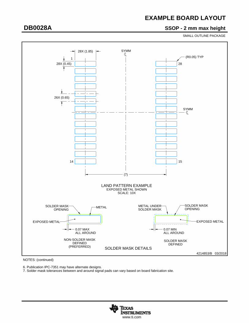
www.ti.com
EXAMPLE BOARD LAYOUT
0.07 MAXALL AROUND
0.07 MINALL AROUND
28X (1.85)
28X (0.45)
26X (0.65)
(7)
(R0.05) TYP
SSOP - 2 mm max heightDB0028ASMALL OUTLINE PACKAGE
4214853/B 03/2018
NOTES: (continued) 6. Publication IPC-7351 may have alternate designs. 7. Solder mask tolerances between and around signal pads can vary based on board fabrication site.
LAND PATTERN EXAMPLEEXPOSED METAL SHOWN
SCALE: 10X
SYMM
SYMM
1
14 15
28
15.000
METALSOLDER MASKOPENING
METAL UNDERSOLDER MASK
SOLDER MASKOPENING
EXPOSED METALEXPOSED METAL
SOLDER MASK DETAILS
NON-SOLDER MASKDEFINED
(PREFERRED)
SOLDER MASKDEFINED

www.ti.com
EXAMPLE STENCIL DESIGN
28X (1.85)
28X (0.45)
26X (0.65)
(7)
(R0.05) TYP
SSOP - 2 mm max heightDB0028ASMALL OUTLINE PACKAGE
4214853/B 03/2018
NOTES: (continued) 8. Laser cutting apertures with trapezoidal walls and rounded corners may offer better paste release. IPC-7525 may have alternate design recommendations. 9. Board assembly site may have different recommendations for stencil design.
SOLDER PASTE EXAMPLEBASED ON 0.125 mm THICK STENCIL
SCALE: 10X
SYMM
SYMM
1
14 15
28
IMPORTANT NOTICE
Texas Instruments Incorporated (TI) reserves the right to make corrections, enhancements, improvements and other changes to itssemiconductor products and services per JESD46, latest issue, and to discontinue any product or service per JESD48, latest issue. Buyersshould obtain the latest relevant information before placing orders and should verify that such information is current and complete.TI’s published terms of sale for semiconductor products (http://www.ti.com/sc/docs/stdterms.htm) apply to the sale of packaged integratedcircuit products that TI has qualified and released to market. Additional terms may apply to the use or sale of other types of TI products andservices.Reproduction of significant portions of TI information in TI data sheets is permissible only if reproduction is without alteration and isaccompanied by all associated warranties, conditions, limitations, and notices. TI is not responsible or liable for such reproduceddocumentation. Information of third parties may be subject to additional restrictions. Resale of TI products or services with statementsdifferent from or beyond the parameters stated by TI for that product or service voids all express and any implied warranties for theassociated TI product or service and is an unfair and deceptive business practice. TI is not responsible or liable for any such statements.Buyers and others who are developing systems that incorporate TI products (collectively, “Designers”) understand and agree that Designersremain responsible for using their independent analysis, evaluation and judgment in designing their applications and that Designers havefull and exclusive responsibility to assure the safety of Designers' applications and compliance of their applications (and of all TI productsused in or for Designers’ applications) with all applicable regulations, laws and other applicable requirements. Designer represents that, withrespect to their applications, Designer has all the necessary expertise to create and implement safeguards that (1) anticipate dangerousconsequences of failures, (2) monitor failures and their consequences, and (3) lessen the likelihood of failures that might cause harm andtake appropriate actions. Designer agrees that prior to using or distributing any applications that include TI products, Designer willthoroughly test such applications and the functionality of such TI products as used in such applications.TI’s provision of technical, application or other design advice, quality characterization, reliability data or other services or information,including, but not limited to, reference designs and materials relating to evaluation modules, (collectively, “TI Resources”) are intended toassist designers who are developing applications that incorporate TI products; by downloading, accessing or using TI Resources in anyway, Designer (individually or, if Designer is acting on behalf of a company, Designer’s company) agrees to use any particular TI Resourcesolely for this purpose and subject to the terms of this Notice.TI’s provision of TI Resources does not expand or otherwise alter TI’s applicable published warranties or warranty disclaimers for TIproducts, and no additional obligations or liabilities arise from TI providing such TI Resources. TI reserves the right to make corrections,enhancements, improvements and other changes to its TI Resources. TI has not conducted any testing other than that specificallydescribed in the published documentation for a particular TI Resource.Designer is authorized to use, copy and modify any individual TI Resource only in connection with the development of applications thatinclude the TI product(s) identified in such TI Resource. NO OTHER LICENSE, EXPRESS OR IMPLIED, BY ESTOPPEL OR OTHERWISETO ANY OTHER TI INTELLECTUAL PROPERTY RIGHT, AND NO LICENSE TO ANY TECHNOLOGY OR INTELLECTUAL PROPERTYRIGHT OF TI OR ANY THIRD PARTY IS GRANTED HEREIN, including but not limited to any patent right, copyright, mask work right, orother intellectual property right relating to any combination, machine, or process in which TI products or services are used. Informationregarding or referencing third-party products or services does not constitute a license to use such products or services, or a warranty orendorsement thereof. Use of TI Resources may require a license from a third party under the patents or other intellectual property of thethird party, or a license from TI under the patents or other intellectual property of TI.TI RESOURCES ARE PROVIDED “AS IS” AND WITH ALL FAULTS. TI DISCLAIMS ALL OTHER WARRANTIES ORREPRESENTATIONS, EXPRESS OR IMPLIED, REGARDING RESOURCES OR USE THEREOF, INCLUDING BUT NOT LIMITED TOACCURACY OR COMPLETENESS, TITLE, ANY EPIDEMIC FAILURE WARRANTY AND ANY IMPLIED WARRANTIES OFMERCHANTABILITY, FITNESS FOR A PARTICULAR PURPOSE, AND NON-INFRINGEMENT OF ANY THIRD PARTY INTELLECTUALPROPERTY RIGHTS. TI SHALL NOT BE LIABLE FOR AND SHALL NOT DEFEND OR INDEMNIFY DESIGNER AGAINST ANY CLAIM,INCLUDING BUT NOT LIMITED TO ANY INFRINGEMENT CLAIM THAT RELATES TO OR IS BASED ON ANY COMBINATION OFPRODUCTS EVEN IF DESCRIBED IN TI RESOURCES OR OTHERWISE. IN NO EVENT SHALL TI BE LIABLE FOR ANY ACTUAL,DIRECT, SPECIAL, COLLATERAL, INDIRECT, PUNITIVE, INCIDENTAL, CONSEQUENTIAL OR EXEMPLARY DAMAGES INCONNECTION WITH OR ARISING OUT OF TI RESOURCES OR USE THEREOF, AND REGARDLESS OF WHETHER TI HAS BEENADVISED OF THE POSSIBILITY OF SUCH DAMAGES.Unless TI has explicitly designated an individual product as meeting the requirements of a particular industry standard (e.g., ISO/TS 16949and ISO 26262), TI is not responsible for any failure to meet such industry standard requirements.Where TI specifically promotes products as facilitating functional safety or as compliant with industry functional safety standards, suchproducts are intended to help enable customers to design and create their own applications that meet applicable functional safety standardsand requirements. Using products in an application does not by itself establish any safety features in the application. Designers mustensure compliance with safety-related requirements and standards applicable to their applications. Designer may not use any TI products inlife-critical medical equipment unless authorized officers of the parties have executed a special contract specifically governing such use.Life-critical medical equipment is medical equipment where failure of such equipment would cause serious bodily injury or death (e.g., lifesupport, pacemakers, defibrillators, heart pumps, neurostimulators, and implantables). Such equipment includes, without limitation, allmedical devices identified by the U.S. Food and Drug Administration as Class III devices and equivalent classifications outside the U.S.TI may expressly designate certain products as completing a particular qualification (e.g., Q100, Military Grade, or Enhanced Product).Designers agree that it has the necessary expertise to select the product with the appropriate qualification designation for their applicationsand that proper product selection is at Designers’ own risk. Designers are solely responsible for compliance with all legal and regulatoryrequirements in connection with such selection.Designer will fully indemnify TI and its representatives against any damages, costs, losses, and/or liabilities arising out of Designer’s non-compliance with the terms and provisions of this Notice.
Mailing Address: Texas Instruments, Post Office Box 655303, Dallas, Texas 75265Copyright © 2018, Texas Instruments Incorporated