Embed Size (px)
Citation preview

Pericom Semiconductor Corp.
www.pericom.com
Page 1 of 1 4/12/2016
AN377
AN377
PCIe Gen3 ReDriver: PI3EQX8908A Trace Extension, Configuration, and Layout Guide
Table of Contents
1 Introduction.............................................................................. ............................... ........................................... 2
2 Extending Length with ReDriver ............................................................ ............................................................ 2
3 External Components Requirement of PCIe Switch.............. ... ... ... ... ............................................................. 4
4 PI3EQX8908A EQ/FG/SW Setting ......................................... ........................................................................... 5
5 PCIe 3.0 Preset Test.................................................................................... ...................................................... 8
6 Output Eye Diagrams Resulted in Various EQ Settings ................................................................................... 10
7 Layout Suggestions to Reduce Crosstalk .........................................................................................................14
8 PI3EQX8908A Typical Reference Circuit............................................ .............................................................15
9 Power Consumption Measurement...................................................... ............................................................16
10 Errata.................................................................................................. ..............................................................17

Pericom Semiconductor Corp.
www.pericom.com
Page 2 of 2 4/12/2016
AN377
AN377
1. Introduction:
Pericom Semiconductor’s PI3EQX8908A is a PCIe, 8 differential channels ReDriver™. The device provides programmable linear equalization, output swing and gain, by either pin strapping option or I2C Control, to optimize performance over a variety of physical mediums by reducing Inter-symbol interference. The PI3EQX8908A supports eight 100-Ohm Differential CML data I/O’s and extends the signals across other distant data pathways on the user’s platform. The programmable settings can be applied easily via pins, software (I2C) or loaded via an external EEPROM. When operating in the EEPROM mode, the configuration information is automatically loaded on power up, which eliminates the need for an external microprocessor or software driver. The PI3EQX8908A offers fully Linear Transfer function to fully comply with all PCIe 3 Link Training signals 2. Extending Length with ReDriver
PCI-SIG provides PCI Express compliance tests that are utilized for testing PCI Express systems . The below PCI Express 3.0 TX Compliance Test use PCI Sigtest320 to check the test result (Figure 1) Sigtest P4 Eye Result" Test 1 - without re-driver
Test 2 - without re-driver
Pericom Semiconductor Corp.
www.pericom.com
Page 3 of 3 4/12/2016
AN377
AN377
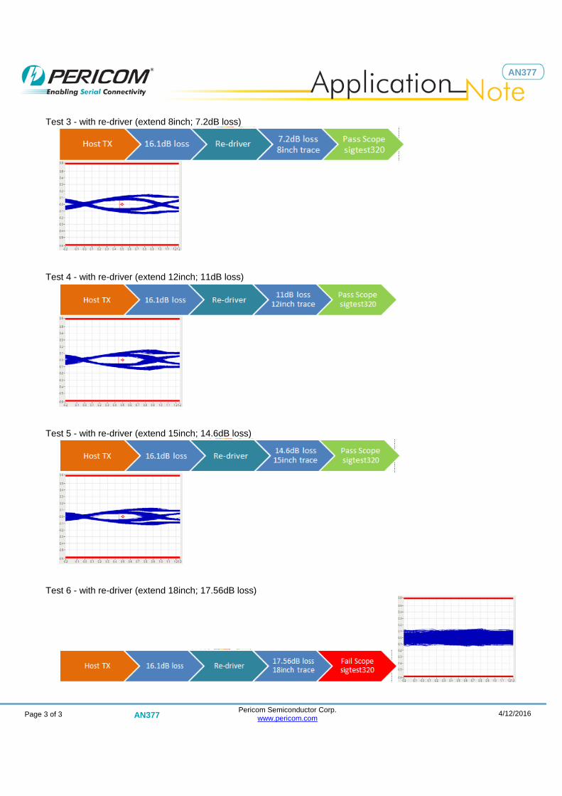
Test 3 - with re-driver (extend 8inch; 7.2dB loss)
Test 4 - with re-driver (extend 12inch; 11dB loss)
Test 5 - with re-driver (extend 15inch; 14.6dB loss)
Test 6 - with re-driver (extend 18inch; 17.56dB loss)

Pericom Semiconductor Corp.
www.pericom.com
Page 4 of 4 4/12/2016
AN377
AN377
Figure 1. Extent length after add ReDriver 3. External Components Requirement of PCIe Switch
If the PCIE MUX implement in the system which can’t tolerance DC level 3.3V, please add AC coupling cap with 200Kohm to GND as below diagram
Figure 2. Add external component if work with Mux
MB
CPU board 1
AC COUPLING CAPS1
PI3EQX8908A
CPU board 1
Tx
Add on card
CPU
AC COUPLING CAPS4
Block Diagram1
Rx
Rx
MUX
Rx
CPU
Rx
AC COUPLING CAPS4
Tx
HOST
Rx
AC COUPLING CAPS4
AC COUPLING CAPS1
Rx
AC COUPLING CAPS3
If MUX can't tolerance 3.3V DC level, pleaseadd this ciircuit
Block Diagram3
R
200K
Tx
Tx
AC COUPLING CAPS3
MUXAC COUPLING CAPS2
CPU
CPU board 2
AC COUPLING CAPS2
CPU
AC COUPLING CAPS2
PI3EQX8908A
PI3EQX8908A
If AC coupling cap place after MUX no needadd extra ciircuit
AC COUPLING CAPS3
Block Diagram2
Tx
AC COUPLING CAPS5
CPU board 2
AC COUPLING CAPS1
Tx

Pericom Semiconductor Corp.
www.pericom.com
Page 5 of 5 4/12/2016
AN377
AN377
4. PI3EQX8908A EQ/FG/SW Setting
Figure 3 below is standard PCIE TX compliance test from Tektronix 25GHz scope sigtest result. We can get the eye height and eye width result then change EQ or FG to get better result. If re-driver input loss is bigger, increase EQ value. If output eye height is not good enough, increase FG value.
Figure 3 PCIE3.0 test setup example
1. EQ: Design transition to PI3EQX8908A from PI3EQX8908 the first step is to understand the changes in the EQ setting values noted in the table below. Note that the 8908A has the same 4dB EQ value steps, but different pin or I2C control values. The change can be from pins (EQA[0..2], EQB[0..2]), or from I2C register (Bytes[3..10]). Reset the EQ value on the 8908A as needed from the EQ/FG tuning procedure below in step 4.
2. DE: There is no De-Emphasis function on the 8908A. The 8908A will automatically reproduce whatever De-
Emphasis value is on the input source. In place of DE, the same pins (FGA[0..1], FGB[0..1]) or I2C registers (Bytes[3..10]) set the FG (Flat Gain) value. (Please see below table for detail ). You will tune the FG as needed from the EQ/FG tuning procedure in step 4.
3. SW: Output Swing – since the 8908A and 8908 OS setting values are very similar, in real application no
change is typically needed. Use same pin or I2C register setting as 8908 for the 8908A as the starting point to tune the EQ and FG settings.
4. FG and EQ Tuning: Below Figure 4 and 5, the PCIE3.0 test setup shows “How to do the EQ/FG tuning”. The EQ mainly relates to the Re-driver input loss, and Figures 6 to 8 shows the typical EQ/FG settings vs. eye height and eye width. The 8908A is tuned from the procedure below.
5. Re-driver input Threshold voltage: When using a Re-driver also needs consider Re-driver input threshold
voltage (Vpp)
Tektronix MSO72504DX
PCIE3.0 test
fixture
P7=-6dBde-emphasis
TX-
CH2
16.1 dBtrace loss
Over 12GHz bandwith Scope
TX+
Source (CPU TX)
ReDriver
TX
Step2:Base on sigtestresult,change ReDriver'sFG/swing setting to get thebetter eye height and eyewidth
Step1: fine turneReDriver EQ matchinput loss
7.2 dBtraceloss
CH1
Sigtest320CTLE-6dB to-12dB + DFE+ loss
PCIE3.0
connector
EQ = 12dB FG = 0dB

Pericom Semiconductor Corp.
www.pericom.com
Page 6 of 6 4/12/2016
AN377
AN377
Figure 4 is a measure example to count swing mVpp for 1010 Preset_4 PCIE compliance pattern
Figure 4

Pericom Semiconductor Corp.
www.pericom.com
Page 7 of 7 4/12/2016
AN377
AN377
Figure 5 - Different EQ vs eye height. Note that higher EQ = higher eye height
Figure 5 Different EQ vs eye height
Figure 6 - Different FG vs eye height. Note that higher FG = higher eye height.
Figure 6 Different FG vs eye height Figure 7 - Different FG vs eye width – Note that lower FG = better eye width
Figure 7 Different FG vs eye width
30.00
80.00
130.00
180.00
230.00
P0 P1 P2 P3 P4 P5 P6 P7 P8 P9 P10
Eye Height (m
V) PI3EQX8908A Eye Height compair by EQ PI3EQX8908A_AA
_FG=0dB / EQ=14 dB_Average
PI3EQX8908A_AA_FG=0dB / EQ=12 dB_Average
PI3EQX8908A_AA_FG=0dB / EQ=8 dB_Average
30.00
80.00
130.00
180.00
230.00
P0 P1 P2 P3 P4 P5 P6 P7 P8 P9 P10
Eye Height (m
V)
PI3EQX8908A Eye Height compair by FG PI3EQX8908A_AA_FG=0dB / EQ=14 dB_Average
PI3EQX8908A_AA_FG=‐2dB / EQ=14 dB_Average
PI3EQX8908A_AA_FG=‐4dB / EQ=14 dB_Average
45.00
55.00
65.00
75.00
85.00
95.00
105.00
P0 P1 P2 P3 P4 P5 P6 P7 P8 P9 P10
Eye W
idth (ps) PI3EQX8908A Eye Width compared to FG
PI3EQX8908A_AA_FG=0dB / EQ=14 dB_AveragePI3EQX8908A_AA_FG=‐2dB / EQ=14 dB_AveragePI3EQX8908A_AA_FG=‐4dB / EQ=14 dB_Average

Pericom Semiconductor Corp.
www.pericom.com
Page 8 of 8 4/12/2016
AN377
AN377
5. PCIe 3.0 Preset Test
From the TX eye test below, we can see that the PI3EQX8908A can reproduce the input eye almost identical for both eye width and eye height. Reproducing the input signal eye is needed for link training compliance.
Figure 8 From preset test result PI3EQX8908A can pass all P10 preset test but PI3EQX8908 can’t identify different De-
emphasis and pre-shoot. This means PI3EQX8908A can both boost the signal and keep the same De-emphasis and Pre-shoot as the input eye, thus PI3EQX8908A will pass through the PCIE3.0 link training signals.
PRESET RESULTS Preset Name Lane Name PreShoot De-Emphasis Vb Result P0 Lane0 0.000 dB -5.307 dB 398.267 mV Pass P01 Lane0 0.000 dB -3.248 dB 504.779 mV Pass P10 Lane0 0.000 dB -8.476 dB 276.516 mV Pass P02 Lane0 0.000 dB -4.459 dB 439.109 mV Pass P03 Lane0 0.000 dB -2.523 dB 548.730 mV Pass P04 Lane0 0.000 dB 0.000 dB 733.690 mV Pass
Input Signal
PI3EQX8908A full linear re-driver EQ=12dB / FG=0dB
PI3EQX8908A linear re-driverLineEQ=12dB / FG=0dB

Pericom Semiconductor Corp.
www.pericom.com
Page 9 of 9 4/12/2016
AN377
AN377
P05 Lane0 1.753 dB 0.000 dB 599.571 mV Pass P06 Lane0 2.421 dB 0.000 dB 555.239 mV Pass P07 Lane0 3.116 dB -5.821 dB 306.757 mV Pass P08 Lane0 3.289 dB -3.392 dB 375.752 mV Pass P09 Lane0 3.089 dB 0.000 dB 514.145 mV Pass
PCIE3.0 Preset P0~P10 specification

Pericom Semiconductor Corp.
www.pericom.com
Page 10 of 10 4/12/2016
AN377
AN377
6. Output Eye Diagrams Resulted in Various EQ Settings
Output Eye Diagram vs. Input FR4 trace and EQ setting at 8Gbps for PI3EQX8908A
Figure 6c: Output Eye Opening with Input Equalization, 8.0 Gbps, Vdd=3.0V, 25C Using PRBS 2^23-1 pattern, Input Swing=800mVd, Output Swing= 1000mV FG=10 (0dB) Trace=12-in(5.16dB loss)
EQ=0000(3.0dB)
EQ=0001(4.0dB)
EQ=0010(5.0dB)
EQ=0011(6.0dB)
EQ=0100(7.0dB)
EQ=0101(8.0dB)
EQ=0110(9.0dB)
EQ=0111(10dB)
EQ=1000(11dB)
EQ=1001(12dB)
EQ=1010(12.5dB)
EQ=1011(13 dB)
EQ=1100(13.5dB)
EQ=1101(14.0dB)
EQ=1110(14.5dB)
EQ=1111(15.0dB)

Pericom Semiconductor Corp.
www.pericom.com
Page 11 of 11 4/12/2016
AN377
AN377
Figure 6e: Output Eye Opening with Input Equalization, 8.0 Gbps, Vdd=3.0V, 25C Using PRBS 2^23-1 pattern, Input Swing=800mVd, Output Swing= 1000mV FG=10 (0dB) Trace=24-in(10.32dB loss)
EQ=0000(3.0dB)
EQ=0001(4.0dB)
EQ=0010(5.0dB)
EQ=0011(6.0dB)
EQ=0100(7.0dB)
EQ=0101(8.0dB)
EQ=0110(9.0dB)
EQ=0111(10dB)
EQ=1000(11dB)
EQ=1001(12dB)
EQ=1010(12.5dB)
EQ=1011(13 dB)
EQ=1100(13.5dB)
EQ=1101(14.0dB)
EQ=1110(14.5dB)
EQ=1111(15.0dB)

Pericom Semiconductor Corp.
www.pericom.com
Page 12 of 12 4/12/2016
AN377
AN377
Figure 6g: Output Eye Opening with Input Equalization, 8.0 Gbps, Vdd=3.0V, 25C Using PRBS 2^23-1 pattern, Input Swing=800mVd, Output Swing= 1000mV FG=10 (0dB) Trace=36-in (15.4dB loss)
EQ=0000(3.0dB)
EQ=0001(4.0dB)
EQ=0010(5.0dB)
EQ=0011(6.0dB)
EQ=0100(7.0dB)
EQ=0101(8.0dB)
EQ=0110(9.0dB)
EQ=0111(10dB)
EQ=1000(11dB)
EQ=1001(12dB)
EQ=1010(12.5dB)
EQ=1011(13 dB)
EQ=1100(13.5dB)
EQ=1101(14.0dB)
EQ=1110(14.5dB)
EQ=1111(15.0dB)

Pericom Semiconductor Corp.
www.pericom.com
Page 13 of 13 4/12/2016
AN377
AN377
7. Layout Suggestions to Reduce Crosstalk

Pericom Semiconductor Corp.
www.pericom.com
Page 14 of 14 4/12/2016
AN377
AN377
8. PI3EQX8908A Typical Reference Circuit
R7
0 ohm or NCD2RX_N
EQB2
RX
Cn
R18
0 ohm or NC
VDD_3.3V
SDA/DEMA0/FGA0
PI3EQX8908/80908A/10908ZLE APPLICATION SCHEMATIC A02Custom
2 4Monday , October 19, 2015
Size Document Name Rev
Date: Sheet of
Pericom Semiconductor Corporation
SD
A/D
EM
A0/
FG
A0
R17
0 ohm or NC
D2RX_P
I2C
_R
ST
/VO
D0
/SW
0
C18
0.1u_0402
reserve for debug purpose
8Gbps
D1RX_P
PRSNT#
R27
0 ohm or NC
VO
D1
/SW
1
I2C SCL / EEPROM SCL
C4 0.176uF~0.265uF_0402
D0RX_P
EQA0
R8
0 ohm or NC
Cn
Speed
C17
0.1u_0402
TX
VDD_3.3V
D2RX_P
R12
0 oh
m o
r N
C
SC
L/D
EM
A1/
FG
A1
VDD_3.3V
VDD_3.3V
AD
2/E
QB
1
D1
LED_R
1 2
SCL/DEMA1
Cn
R5
0 ohm or NC
TX
H1RX_P
R14
0 o
hm o
r N
C
VDD_3.3V
I2C SDA / EEPROM SDA
D1TX_N
R6
0 ohm or NC
R16
0 ohm or NC
VDD_3.3V
H0TX_P
U1
PI3EQX8908/8908A/10908ZLE@TQFN54
19 204544
9
10
4342
1112
4039
13
14
3837
1516
54
21 22
18
23 24
53
3233
5
41
52
3435
43
50 49
36
8
21
4876
4725 26
172829
46
3031
27
51
EQ
A2
EQ
A1
B0TX+B0TX-
VDD
A0RX+
B1TX+B1TX-
A0RX-A1RX+
B2TX+B2TX-
A1RX-
VDD
B3TX+B3TX-
A2RX+A2RX-
DE
MB
1/F
GB
1/A
D0
EQ
A0
RX
DE
T
A3RX-
EQ
B2
VO
D1/
SW
1
DE
MB
0/F
GB
0/A
D1
A1TX-A1TX+
B2RX+
VDD
PR
SN
T#
A0TX-A0TX+
B1RX-B1RX+
DE
MA
1/F
GA
1/S
CL
DE
MA
0/F
GA
0/S
DA
VDD
B3RX-
B0RX-B0RX+E
NI2
CB3RX+B2RX-
EQ
B1/
AD
2I2
C_R
eset
#/V
OD
0/S
W0
SD
_TH
A3RX+A3TX-A3TX+
EQ
B0/
AD
3
A2TX-A2TX+
ALL
_DO
NE
#
VD
D
I2C SDA /EEPROMSDA
IC Part
VDD_3.3V
EQA2
H3TX_P
SCL/DEMA1/FGA1
SCL/DEMA1/FGA1A
LL_D
ON
E#
R23
0 ohm or NC
D2TX_P
VDD_3.3V
VDD_3.3V
H3TX_N
C13 0.176uF~0.265uF_0402
R320 ohm or NC
NC
H0TX_N
C16 0.176uF~0.265uF_0402
I2C SDA /EEPROMSDA
R21
0 ohm or NC
RX
PI3EQX10908
R19
0 ohm or NC
I2C SCL /EEPROMSCL
RX
_DE
T
VDD_3.3V
PR
SN
T#
R310 ohm or NC
ALL_DONE#
DE
MB
1/F
GB
1/A
D0
ENI2C=Low (Pin strap control)R11=NC , R19=on
DEMB1/FGB1/AD0
4.7nF
R10 ohm or NC
R10
2K ohm
Connect to I2C SDA
C15 0.176uF~0.265uF_0402
H1TX_P
R28
0 ohm or NC
C6 0.176uF~0.265uF_0402
SDA/DEMA0/FGA0
EN
I2C
C3 0.176uF~0.265uF_0402
R31=0ohm
DEMB0/FGB0/AD1
C9 0.176uF~0.265uF_0402
R31=0ohm
C10 0.176uF~0.265uF_0402
EQ
A0
R13
0 oh
m o
r N
C
Connect to EEPROM SCL
10GBASE-KR:
VDD_3.3V
D0TX_N
R29
0 ohm or NC
I2C SDA /EEPROMSDA
D3TX_P
R32
0 ohm or NC
10Gbps
VDD_3.3V
R2
0 ohm or NC
C5 0.176uF~0.265uF_0402
SCL/DEMA1/FGA1
+EC1
1.0uF_0805
SD
_T
H
I2C SCL /EEPROMSCL
D1TX_P
C11 0.176uF~0.265uF_0402
R32=NC
SCL/DEMA1/FGA1
Attention the IC part
VDD_3.3V
D0RX_N
SDA/DEMA0/FGA0
C7 0.176uF~0.265uF_0402
H0RX_N
ENI2C
R310 ohm
I2C SCL /EEPROMSCL
Location
SDA/DEMA0
D2TX_N
Connect to EEPROM SDA
I2C_RST/VOD0/SW0
R20
0 ohm or NC
D1RX_N
D3TX_N
C14 0.176uF~0.265uF_0402
H1TX_N
R30
0 ohm or NC
SCL/DEMA1/FGA1
0.176uF~0.265uF
H3RX_P
EQ
A2
R15
0 ohm or NC
ENI2C=NC(Master mode)R11=NC, R19=NC
VOD1/SW1
10GBASE-KX4:
SD_TH
C1 0.176uF~0.265uF_0402
VDD_3.3V
R33
0 ohm or NC
SDA/DEMA0/FGA0
H2RX_P
R3
0 ohm or NC
D0TX_P
R9
0 ohm or NC
Connect to I2C SCL
AD3/EQB0
H2TX_P
C8 0.176uF~0.265uF_0402
HOST
PI3EQX8908/PI3EQX8908A
VDD_3.3V
R32=0ohm
C2 0.176uF~0.265uF_0402
H2TX_N
R24
0 ohm or NC
NC
H3RX_N
EQ
B2
R26
0 ohm or NC
Device orConnector
and differential TX AC coupling capacitor value.
D2RX_N
R22
0 ohm or NC
R31=NC
VDD_3.3V
H2RX_N
DE
MB
0/F
GB
0/A
D1
C12 0.176uF~0.265uF_0402
R25
0 ohm or NC
R32=0ohm
H1RX_N
AD
3/E
QB
0
SDA/DEMA0/FGA0
R11
0 ohm or NC
0.1uF
VDD_3.3V
R4
0 ohm or NC
ENI2C=High (I2C control)R11=on, R19=NC
H0RX_PE
QA
1

Pericom Semiconductor Corp.
www.pericom.com
Page 15 of 15 4/12/2016
AN377
AN377
9. Power Consumption Measurement
PI3EQX8908A Power Consumption Measurement 1, Channel Current when enabled separately by register bits at constant temp. Signal Detector=Enabled A3 A2 A1 A0 B3 B2 B1 B0 Idd Unit:SW=11(1200mV) FG=10/11 EQ=0000/1111
Disabled 2.3 Enabled 33.9 Enabled 34.0 Enabled 33.7 Enabled 33.8 Enabled 34.2 Enabled 34.1 Enabled 33.9 Enabled 34.3
Enabled 254.6
Signal Detector=Enabled A3 A2 A1 A0 B3 B2 B1 B0 Idd Unit:SW=00(900mV) FG=10/11 EQ=0000/1111
Disabled 2.3 Enabled 32.7 Enabled 32.7 Enabled 32.4 Enabled 32.5 Enabled 32.9 Enabled 32.8 Enabled 32.7 Enabled 33.0
Enabled 244.8
Signal Detector=Disabled A3 A2 A1 A0 B3 B2 B1 B0 Idd Unit:SW=11(1200mV) FG=10/11 EQ=0000/1111
Disabled 2.3 Enabled 29.1 Enabled 29.3 Enabled 28.9 Enabled 29.0 Enabled 29.4 Enabled 29.3 Enabled 29.1 Enabled 29.5
Enabled 216.2

Pericom Semiconductor Corp.
www.pericom.com
Page 16 of 16 4/12/2016
AN377
AN377
10 Errata
NA


![M.2 PCIe Gen3 SSD · 2.0 PRODUCT SPECIFICATION. 2.1 Capacity [Table 2] User Addressable Sectors. NOTE: 1) Gigabyte(GB) = 1,000,000,000 Bytes, 1 Sector = 512Bytes. 2.2 Performance](https://img.pdfslide.us/doc/110x75/5e19e3e5e9584110d31b2f25/m2-pcie-gen3-ssd-20-product-specification-21-capacity-table-2-user-addressable.jpg)