Embed Size (px)
Citation preview
PCIe based readout
U. Marconi, INFN BolognaCERN, May 2013
2
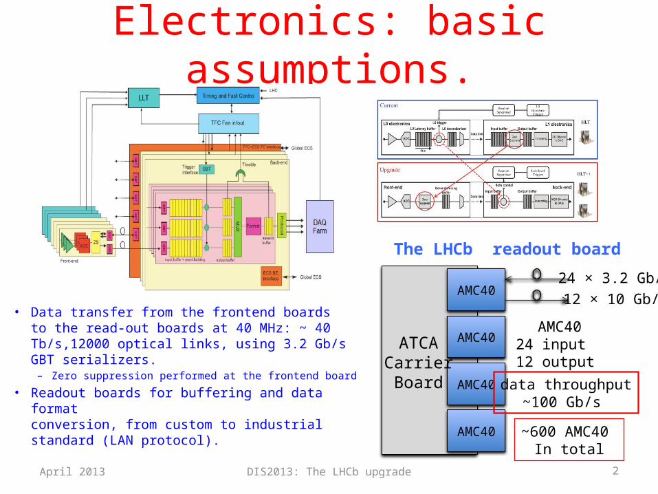
Electronics: basic assumptions.
• Data transfer from the frontend boardsto the read-out boards at 40 MHz: ~ 40 Tb/s,12000 optical links, using 3.2 Gb/s GBT serializers.– Zero suppression performed at the frontend board
• Readout boards for buffering and data formatconversion, from custom to industrial standard (LAN protocol).
April 2013 DIS2013: The LHCb upgrade
AMC40
AMC40
AMC40
AMC40
24 × 3.2 Gb/s
ATCACarrierBoard
12 × 10 Gb/s
AMC40 24 input12 output
data throughput~100 Gb/s
~600 AMC40 In total
The LHCb readout board

DAQ Network
Implement the InfiniBand protocol on the AMC40 FPGAs:not an easy task though …
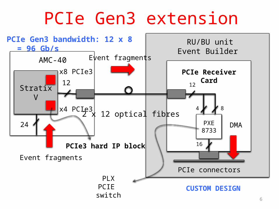
Why not try then with PCIe Gen3?One would need just a suitable receiver card on the server …Changing the architecture of course
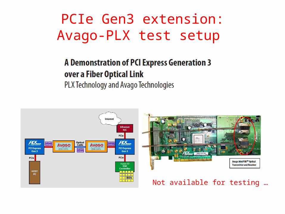
PCIe Gen3 extension:Avago-PLX test setup
Not available for testing …
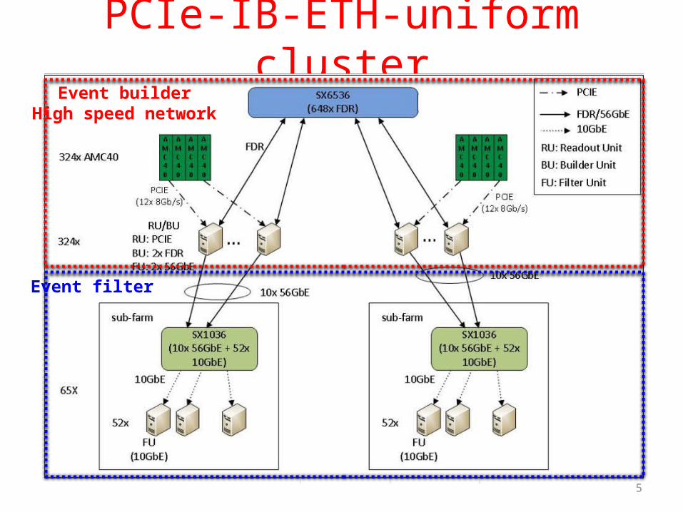
PCIe-IB-ETH-uniform cluster
5
Event builderHigh speed network
Event filter
6
PCIe Receiver Card
PCIe connectors
AMC-40
PXE8733
2 x 12 optical fibres
12
4 8
16
RU/BU unitEvent Builder
Stratix V12
24
PCIe Gen3 bandwidth: 12 x 8 = 96 Gb/s
x8 PCIe3
x4 PCIe3
Event fragments
DMA
PCIe3 hard IP block
PLXPCIE switch
PCIe Gen3 extension
Event fragments
CUSTOM DESIGN
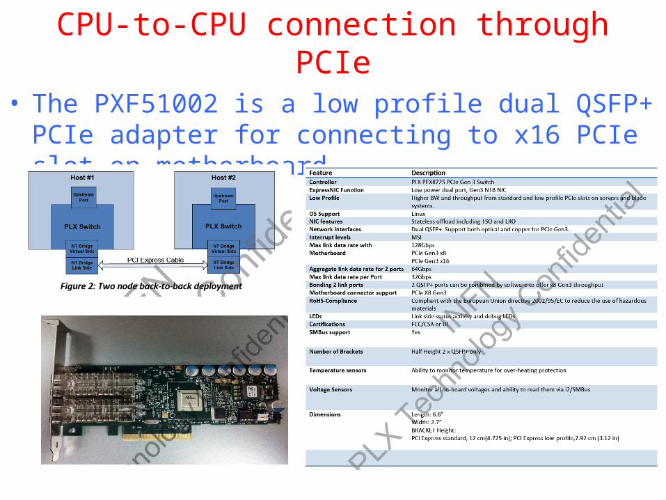
CPU-to-CPU connection through PCIe
• The PXF51002 is a low profile dual QSFP+ PCIe adapter for connecting to x16 PCIe slot on motherboard.
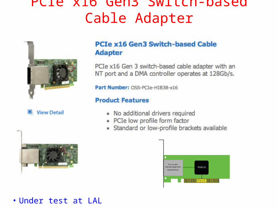
PCIe x16 Gen3 Switch-based Cable Adapter
• Under test at LAL

9
PXF5102
PCIe connectors
AMC-40
3x4 optical fibres
x8
RU/BU unitEvent Builder
Stratix V
24
PCIe Gen3 bandwidth: 12 x 8 = 96 Gb/s
x4 PCIe3
Event fragmentsfrom FEE
PCIe3 hard IP block
PXF510028725 PCIE switch
PXF51002 based solution
Event fragments
x8
x4
x4
x4
x4 PXF5102
QSFP+
10
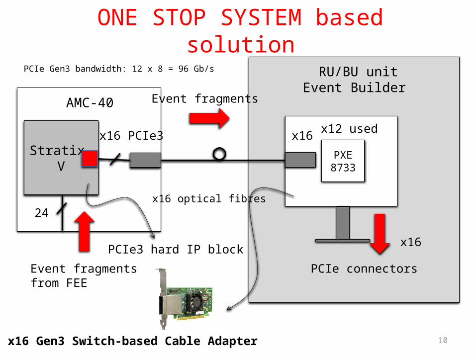
PCIe connectors
AMC-40
x16 optical fibres
RU/BU unitEvent Builder
Stratix V
24
PCIe Gen3 bandwidth: 12 x 8 = 96 Gb/s
x16 PCIe3
Event fragmentsfrom FEE
PCIe3 hard IP block
ONE STOP SYSTEM based solution
Event fragments
x16
x16 x12 used
PXE8733
PCIe x16 Gen3 Switch-based Cable Adapter
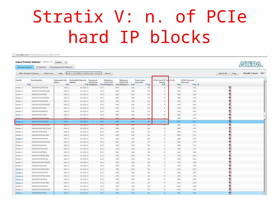
Stratix V: n. of PCIe hard IP blocks
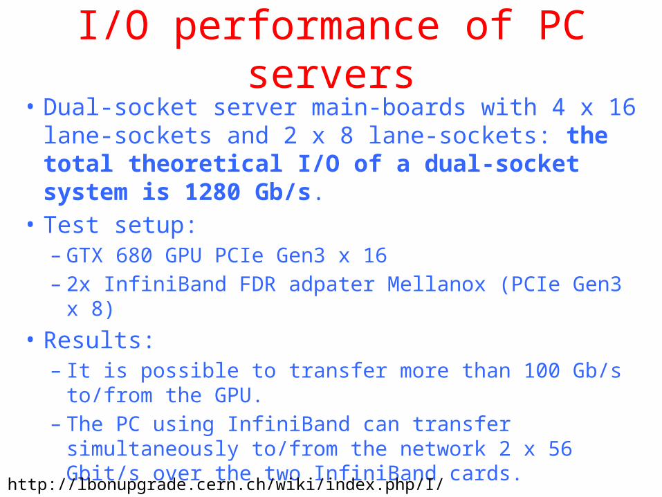
I/O performance of PC servers• Dual-socket server main-boards with 4 x 16 lane-
sockets and 2 x 8 lane-sockets: the total theoretical I/O of a dual-socket system is 1280 Gb/s.
• Test setup:– GTX 680 GPU PCIe Gen3 x 16– 2x InfiniBand FDR adpater Mellanox (PCIe Gen3 x 8)
• Results:– It is possible to transfer more than 100 Gb/s to/from the
GPU.– The PC using InfiniBand can transfer simultaneously
to/from the network 2 x 56 Gbit/s over the two InfiniBand cards.http://lbonupgrade.cern.ch/wiki/index.php/I/O_performance_of_PC_servers
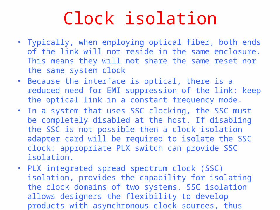
Clock isolation• Typically, when employing optical fiber, both ends of the link will not
reside in the same enclosure. This means they will not share the same reset nor the same system clock
• Because the interface is optical, there is a reduced need for EMI suppression of the link: keep the optical link in a constant frequency mode.
• In a system that uses SSC clocking, the SSC must be completely disabled at the host. If disabling the SSC is not possible then a clock isolation adapter card will be required to isolate the SSC clock: appropriate PLX switch can provide SSC isolation.
• PLX integrated spread spectrum clock (SSC) isolation, provides the capability for isolating the clock domains of two systems. SSC isolation allows designers the flexibility to develop products with asynchronous clock sources, thus removing the need for a single clock source for all PCIe components in a system.– When you enable the switch, its Port 0 operates in the spread-spectrum-clocking
domain, and the other ports operate in the constant-frequency-clock domain.
Summary
• PCIe Gen3 appears a viable solution to inject data from the AMC40 to the EFF servers.
• We are ready to start testing PCIe Gen3 CPU-to-CPU based connections, relying on commercial PCIe cable adapters, linked with optical fibres.
• Next step is to replace one of the CPU with a Stratix V FPGA.