Embed Size (px)
Citation preview

Page 1 of 51 13 June 2011, Version 1.0 PCIe Gen3 MOI
PCI Express 3.0CEM Stressed Eye Calibration and Receiver Testing
Methods of Implementation using Tektronix BERTScope BSA85C Analyzer,
CR125A Clock Recovery, DPP125B De-Emphasis Processor, and Series 70000 Real-Time Oscilloscope
14 June 2011, Version 1.0 55W-27105-0

Page 2 of 51 13 June 2011, Version 1.0 PCIe Gen3 MOI
Copyright ©Tektronix. All rights reserved. Licensed software products are owned by Tektronix and are protected by United States copyright laws and international treaty provisions.
Tektronix products are covered by U.S. and foreign patents, issued and pending. Information in this publication supersedes that in all previously published material. Specifications and price change privileges reserved.
TEKTRONIX, TEK, BERTScope, and RT-Eye are registered trademarks of Tektronix, Inc.
Contacting Tektronix
Tektronix, Inc. 14200 SW Karl Braun Drive or P.O. Box 500 Beaverton, OR 97077 USA

Page 3 of 51 13 June 2011, Version 1.0 PCIe Gen3 MOI
Table of Contents
1 Overview.....................................................................................................................................8 2 Equipment and Software Requirements .................................................................................9
2.1 BSA85C Bit Error Ratio Analyzer ......................................................................................9 2.2 CR125A Clock Recovery Instrument ..................................................................................9 2.3 DPP125B Digital Pre-Emphasis Processor..........................................................................9 2.4 PCISIG Compliance Boards ..............................................................................................10
2.4.1 PCISIG Compliance Base Board (CBB), Main.....................................................10 2.4.2 PCISIG Compliance Base Board (CBB), Riser.....................................................11 2.4.3 PCISIG Compliance Load Board (CLB) ...............................................................12
2.5 Real-Time Oscilloscope.....................................................................................................12 2.6 PCISIG SIGTEST Analysis Software ...............................................................................12 2.7 DMI Combiner...................................................................................................................13 2.8 ATX Power Supply............................................................................................................13 2.9 Cables.................................................................................................................................13 2.10 Tx Repeater........................................................................................................................14
3 Receiver Jitter Tolerance Test ...............................................................................................15 3.1 Add-In Card Testing ..........................................................................................................15
3.1.1 Add-In Card Test Equipment Connections............................................................15 3.2 Host Testing .......................................................................................................................17
3.2.1 Method 1: Manual Loopback Test Equipment Connections .................................18 3.2.2 Method 2: Pattern-Initiated Loopback Test Equipment Connections....................19
3.3 Select Test Configuration ..................................................................................................21 3.4 Loopback Initiation............................................................................................................21
3.4.1 Background............................................................................................................21 3.4.2 Load Loopback A/B Pattern ..................................................................................22 3.4.3 Initiate Loopback ...................................................................................................23 3.4.4 Check Detector Synchronization ...........................................................................24
3.5 Loopback Tips ...................................................................................................................24 3.6 BER Testing.......................................................................................................................25
4 Appendix A, Stressed Eye Calibration ..................................................................................26 4.1 Set DPP Clock to Data Skew.............................................................................................26
4.1.1 Connection and Configuration...............................................................................26 4.2 SJ and DPP Amplitude Calibration....................................................................................29
4.2.1 Required Equipment ..............................................................................................29 4.2.2 Test Equipment Connections .................................................................................29
4.3 Calibrate DPP Output Amplitude ......................................................................................30 4.4 Calibrate Sinusoidal Jitter (SJ)...........................................................................................33 4.5 Calibrate the Stressed Eye using SIGTEST on the RT Scope ...........................................35
4.5.1 Amplitude Calibration ...........................................................................................35 4.6 Calibrate Random Jitter (RJ) .............................................................................................41 4.7 Calibrate Differential Mode Interference...........................................................................43
4.7.1 Configuration for Differential Mode Interference Calibration ..............................43 4.8 Calibrate Sinusoidal Interference.......................................................................................44
Page 4 of 51 13 June 2011, Version 1.0 PCIe Gen3 MOI
4.9 Eye Height and Eye Width Calibration .............................................................................46 4.9.1 Configuration for Host (System) Calibration of Eye Height/Width......................46 4.9.2 Equipment Setup for AIC Eye Height/Width Calibration .....................................47 4.9.3 Eye Height/Width Calibration Procedure ..............................................................47
4.10 Create Calibrated Configuration File.................................................................................49 5 Appendix B: Optional 100 MHz Multiplier Configuration.................................................50
5.1 Equipment Configuration...................................................................................................50 5.2 Equipment Settings ............................................................................................................50
6 Appendix C: Abbreviations and Acronyms.........................................................................51

Page 5 of 51 13 June 2011, Version 1.0 PCIe Gen3 MOI
List of Figures
Figure 1: BERTScope BSA85C Bit Error Ratio Analyzer............................................................. 9 Figure 2: BERTScope CR125A Clock Recovery Instrument......................................................... 9 Figure 3: BERTScope DPP125B Digital Pre-Emphasis Processor ................................................ 9 Figure 4: PCISIG Compliance Base Board (CBB), Main ............................................................ 10 Figure 5: PCISIG Compliance Base Board (CBB), Riser ........................................................... 11 Figure 6: PCISIG Compliance Load Board (CLB)...................................................................... 12 Figure 7: DPO/DSA70000, MSO70000 Real-Time Oscilloscope .............................................. 12 Figure 8: ATX-Compliant Power Supply .................................................................................... 13 Figure 9: Matched Pair SMA (male) – SMP (female) Cables ..................................................... 13 Figure 10: PCIe Tx Repeater ....................................................................................................... 14 Figure 11: Add-In Card Connection Diagram ............................................................................. 15 Figure 12: Host Connection Diagram (Manual Loopback) ......................................................... 17 Figure 13: Host Connection Diagram (Pattern-Triggered Loopback)......................................... 19 Figure 14: Select BERTScope Analyzer Configuration .............................................................. 21 Figure 15: Set BSA85C Generator to Track Detector User Pattern ............................................ 22 Figure 16: Load Modified Compliance Pattern into Generator ................................................... 23 Figure 17: Page Switch to Toggle Loopback Pattern .................................................................. 23 Figure 18: Auto Align to Optimize Detector Sample Point......................................................... 24 Figure 19: Check that Detector is in Sync ................................................................................... 24 Figure 20: Reset Detector Results................................................................................................ 25 Figure 21: Click the Run Button to Start Test ............................................................................. 25 Figure 22: DPP Timing Calibration Connections........................................................................ 26 Figure 23: Set Stress Levels......................................................................................................... 27 Figure 24: Set Generator Delay ................................................................................................... 27 Figure 25: Find Optimum Delay.................................................................................................. 28 Figure 26: Stress Timing Configuration ...................................................................................... 29 Figure 27: Set Internal Synthesizer.............................................................................................. 30 Figure 28: Load DPP Pattern Preset 4 ......................................................................................... 31 Figure 29: Set Bandwidth ............................................................................................................ 31 Figure 30: Set Average Acquisition............................................................................................. 31 Figure 31: Set for Mean Average Voltage Measurement ............................................................ 32 Figure 32: Open DPP Output Voltage Control ............................................................................ 32 Figure 33: DPP Amplitude Measured at 799 mV using Real-Time Oscilloscope ...................... 33 Figure 34: Turn Off Jitter Sources ............................................................................................... 34 Figure 35: Load DPP Pattern Preset 4 ......................................................................................... 34 Figure 36: Set Record Length and Sample Rate.......................................................................... 35 Figure 37: Adjust Oscilloscope Vertical Scale ............................................................................ 35 Figure 38: View of Waveform for Analysis ................................................................................ 36

Page 6 of 51 13 June 2011, Version 1.0 PCIe Gen3 MOI
Figure 39: Save the Baseline Waveform ..................................................................................... 37 Figure 40: Locate and Load the Saved Waveform File ............................................................... 38 Figure 41: Select Pattern File and Initiate Test............................................................................ 39 Figure 42: Baseline TJ Measured at 18.2 ps ................................................................................ 39 Figure 43: TJ at 30.4 ps................................................................................................................ 40 Figure 44: Set Record Length and Sample Rate........................................................................... 41 Figure 45: Setup for Differential Mode Calibration .................................................................... 43 Figure 46: Set Average Acquisition............................................................................................. 44 Figure 47: Set for Peak-to-Peak Voltage Measurement .............................................................. 44 Figure 48: Measure Average Peak-to-Peak Voltage..................................................................... 45 Figure 49: Equipment Setup for Host (System) Eye Height/Width Calibration ......................... 46 Figure 50: Equipment Setup for AIC Eye Height/Width Calibration.......................................... 47 Figure 51: Transition Eye Height and Non-Transition Eye Height.............................................. 48 Figure 52: Two CR Units Configured as 100 MHz to 8 GHz Multiplier .................................... 50

Page 7 of 51 13 June 2011, Version 1.0 PCIe Gen3 MOI
Revision History
Version Date Summary of Changes 1.0 14 June 2011 Initial Release

Page 8 of 51 13 June 2011, Version 1.0 PCIe Gen3 MOI
1 Overview This document provides procedures for PCI Express Generation 3.0 CEM Receiver testing using Tektronix BERTScope instruments. The procedures cover testing of both Add-In Cards and Host devices, in accordance with the PCI Express Generation 3.0 Card Electro-Mechanical (CEM) specification requirements. These tests utilize standard compliance test boards available from the PCISIG organization.
In addition, Appendix A of this document contains procedures for calibrating the test signal stressed eye using a Real-Time Oscilloscope and SIGTEST signal analysis software.

Page 9 of 51 13 June 2011, Version 1.0 PCIe Gen3 MOI
2 Equipment and Software Requirements
2.1 BSA85C Bit Error Ratio Analyzer The BERTScope BSA85C Bit Error Ratio Analyzer provides test and calibration data patterns, and all five jitter sources required for CEM testing. Option STR (Stressed Eye) is required for CEM receiver testing.
Figure 1: BERTScope BSA85C Bit Error Ratio Analyzer
2.2 CR125A Clock Recovery Instrument The BERTScope CR125A Clock Recovery instrument is used to recover a synchronous clock from the Tx data retransmitted from the DUT. The recovered clock may also be used as a synchronous full rate clock input to the pattern generator in cases where a full rate synchronous clock is not available from the DUT. The instrument allows full control of parameters including loop bandwidth, peaking/damping, and roll-off.
Figure 2: BERTScope CR125A Clock Recovery Instrument
2.3 DPP125B Digital Pre-Emphasis Processor The BERTScope Digital Pre-emphasis Processor DPP125B takes in single-ended data and clock inputs and conditions the signal by adding controllable amounts of pre-emphasis.
Figure 3: BERTScope DPP125B Digital Pre-Emphasis Processor

Page 10 of 51 13 June 2011, Version 1.0 PCIe Gen3 MOI
2.4 PCISIG Compliance Boards PCI Express Generation 3.0 Compliance Boards are available from the PCISIG, www.pcisig.com.
Three boards are necessary for both Add-in Card and Host testing, as shown below.
2.4.1 PCISIG Compliance Base Board (CBB), Main The Main Compliance Base Board (CBB) is used for in conjunction with Compliance Base Board Riser for testing Add-in Cards (AIC). For AIC testing, the Main CBB requires that power be supplied from a standard ATX-compliant PC power supply.
Figure 4: PCISIG Compliance Base Board (CBB), Main
NOTE: For stress calibration, power-in and 100 MHz reference are not required.

Page 11 of 51 13 June 2011, Version 1.0 PCIe Gen3 MOI
2.4.2 PCISIG Compliance Base Board (CBB), Riser The CBB riser is used for AIC testing in conjunction with the CBB Main board. Lane 0 Rx (In) connections to the CBB Riser are indicated below. The CBB Riser also provides the additional channel path to meet the ISI requirements of the PCIe Gen 3 “Long Path.”
Figure 5: PCISIG Compliance Base Board (CBB), Riser

Page 12 of 51 13 June 2011, Version 1.0 PCIe Gen3 MOI
2.4.3 PCISIG Compliance Load Board (CLB)
The Compliance Load Board is connected to the PCIe slot of the Host under test, and provides a means for Rx and Tx connections to the Host.
Figure 6: PCISIG Compliance Load Board (CLB)
2.5 Real-Time Oscilloscope A Real-Time Oscilloscope is used for calibration of the PCIe Gen 3 stress levels. The procedures detailed in this MOI are based on the use of a Tektronix DPO/DSA70000, MSO70000Series real-time oscilloscope. The Oscilloscope captures critical signal information with a four-channel system bandwidth of 20 GHz, combined with high waveform capture capability. Note that jitter analysis requires that SIGTEST software be installed on the oscilloscope, as described below.
Figure 7: DPO/DSA70000, MSO70000 Real-Time Oscilloscope
2.6 PCISIG SIGTEST Analysis Software SIGTEST software is required for CEM stress calibration. It is to be installed on the Real-Time Oscilloscope used for calibration.
SIGTEST software is available directly from the PCISIG, and may be downloaded at: http://www.pcisig.com/specifications/pciexpress/compliance/compliance_library.

Page 13 of 51 13 June 2011, Version 1.0 PCIe Gen3 MOI
2.7 DMI Combiner Differential-Mode Interference (DMI) is added to the stressed Rx test pattern as required by the CEM test specification. When using the single-ended Sinusoidal Interference (SI) output of the BERTScope Analyzer to meet this requirement, the following components can be configured to provide the required DMI:
A Balun (e.g., Narda 4346) to convert the single-ended SI output to a differential signal
Two Couplers (e.g., RF Lambda RFDC5M18G10)
2.8 ATX Power Supply An ATX-compliant power supply is used to provide power to the Compliance Base Board for Add-In Card (AIC) testing.
Figure 8: ATX-Compliant Power Supply
2.9 Cables For connection to the SMP connectors found on the PCISIG Compliance Boards, three pairs of matched SMA (male) – SMP (female),50 Ohm coaxial cables are required for AIC testing. Host testing and calibration require only two pairs of these cables. Cables pictured are Rosenberger cable assembly 101462.
Figure 9: Matched Pair SMA (male) – SMP (female) Cables

Page 14 of 51 13 June 2011, Version 1.0 PCIe Gen3 MOI
In addition, multiple SMA (male) – SMA(male) cables of various lengths are required, as indicated in the equipment setup diagrams for each test and calibration configuration.
2.10 Tx Repeater In situations where the eye diagram of Tx signal from the DUT is not sufficiently open to provide reliable BER testing of the Tx data pattern – typically in Host testing – it is recommended to add a repeater circuit in the Tx return path.
A suitable repeater is available as an Evaluation Board assembly from National Semiconductor, Part Number DS80PCI800EVK: http://www.national.com/pf/DS/DS80PCI800.html#Overview
Figure 10: PCIe Tx Repeater
Page 15 of 51 13 June 2011, Version 1.0 PCIe Gen3 MOI
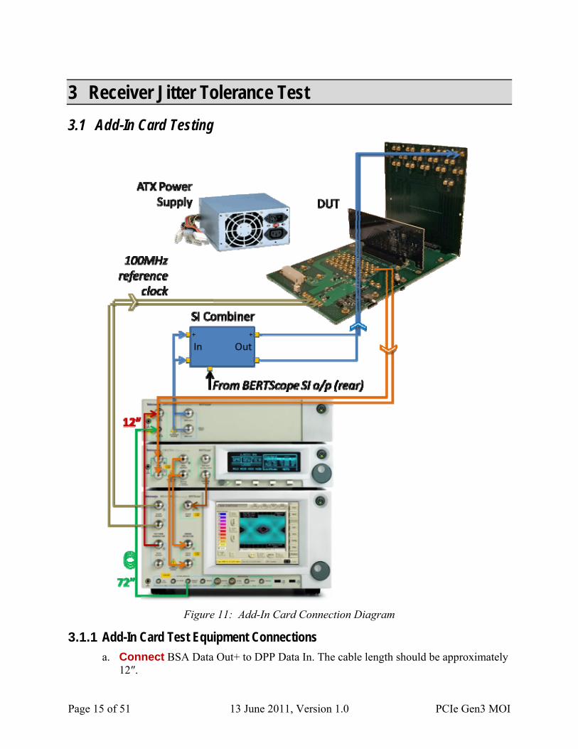
3 Receiver Jitter Tolerance Test
3.1 Add-In Card Testing
Figure 11: Add-In Card Connection Diagram
3.1.1 Add-In Card Test Equipment Connections
a. Connect BSA Data Out+ to DPP Data In. The cable length should be approximately 12″.

Page 16 of 51 13 June 2011, Version 1.0 PCIe Gen3 MOI
b. Connect BSA Subrate Clock Out to DPP Clock In. The cable length should be approximately 72″.
c. Connect the differential Tx output from the CBB-Main (Tx Lane 0) connectors to CR Data– In using a matched SMA to SMP cable set.
d. Connect CR Data Out (+/–) to BSA Detector Data In (+/–) using a matched SMA to SMA cable set.
e. Connect CR Subrate Clock Out to BSA Detector Clock In. This SMA to SMA cable should be as short as possible.
f. Connect the DPP Data Out (+/–) to the input of the SI combiner (+/–) using a matched SMA to SMA cable set.
g. Connect the SI Combiner Out (+/–) to the Rx Lane 0 input on the CBB-Riser card using a matched SMA to SMP cable set.
h. Connect the SI output on the rear connector panel of the BSA to the SI In (Balun input) of the SI Combiner.
i. Connect the BSA Clock Out (+/–) to Ref Clk In on the CBB-Main card using a matched SMA to SMP cable set.
j. Connect the ATX power supply to the power input connector on the CBB-Main board.
k. Insert the DUT into the PCIe slot on the CBB-Main board.
NOTE: The outputs of the DPP unit are AC-coupled, and therefore do not require DC
blocks.

Page 17 of 51 13 June 2011, Version 1.0 PCIe Gen3 MOI
3.2 Host Testing
Figure 12: Host Connection Diagram (Manual Loopback)
NOTE: The Compliance Load Board (CLB) is shown connected in the single lane (x1) configuration. If alternate CLB configurations are used (x4, x8, x16), always connect to the Lane 0 Rx and Tx connectors for the configuration being used.

Page 18 of 51 13 June 2011, Version 1.0 PCIe Gen3 MOI
3.2.1 Method 1: Manual Loopback Test Equipment Connections
a. Connect BSA Data Out+ to DPP Data In. The cable length should be approximately 12″.
b. Connect BSA Subrate Clock Out to DPP Clock In. The cable length should be approximately 72″.
c. Insertthe CLB card into the PCI connector on the Host (DUT).
d. Connect CR Data Out (+/–) to BSA Detector Data In (+/–) using a matched SMA to SMA cable set.
e. Connect CR Subrate Clock Outto BSA Detector Clock In. This SMA to SMA cable should be as short as possible.
f. Connect CR Clock Outto BSA Generator External ClockIn.
g. Connect the DPP Data Out (+/–) to the input of the SI combiner (+/–) using a matched SMA to SMA cable set.
h. Connect the SI combiner (+/–) out to the Rx Lane 0 input on the CBB-Riser card using a matched SMA to SMP cable set.
i. Connect the SI Output on the rear connector panel of the BERTScope Analyzer to the SI input (Balun input) of the SI Combiner.
j. Connect the differential Tx output from the CLB (Tx Lane 0) connectors to Repeater Data In using a matched SMA to SMP cable set.
k. Connect the differential Tx output from the Repeater (+/–) to the CR Data In (+/–) using a matched SMA to SMA cable set.
l. Connect CR Data Out (+/–) to BSA Detector Data In (+/–) using a matched SMA to SMA cable set. This cable set should be at least 39″ long.
m. Connect The differential Tx output from the CBB-Main (Tx Lane 0) connectors to CR Data In using a matched SMA to SMP cable set.
n. Connect3.3 VDC to the power input connector of the Repeater board.

Page 19 of 51 13 June 2011, Version 1.0 PCIe Gen3 MOI
Figure 13: Host Connection Diagram (Pattern-Triggered Loopback)
3.2.2 Method 2: Pattern-Initiated Loopback Test Equipment Connections
a. Connect BSA Data Out+ to DPP Data In. The cable length should be approximately 12″.
b. Connect BSA Subrate Clock Out to DPP Clock In. The cable length should be approximately 72″.
c. Insertthe CLB card into the PCI connector on the Host (DUT).
d. Connect the CLB 100 MHz Clock Out to the Multiplier Clock In (+/–)

Page 20 of 51 13 June 2011, Version 1.0 PCIe Gen3 MOI
e. Connectone output of the Multiplier 8 GHz Clock Out to the BSA Detector Clock In.
f. Connectthe second the Multiplier 8 GHz Clock Out to the BSA Generator External Clock In.
g. Connect the DPP Data Out (+/–) to the input of the SI combiner (+/–) using a matched SMA to SMA cable set.
h. Connect the SI combiner (+/–) out to the Rx Lane 0 input on the CBB-Riser card using a matched SMA to SMP cable set.
i. Connect the SI Output on the rear connector panel of the BERTScope Analyzer to the SI input (Balun input) of the SI Combiner.
j. Connect the differential Tx output from the CLB (Tx Lane 0) connectors to Repeater Data In using a matched SMA to SMP cable set.
k. Connect the differential Tx output from the Repeater (+/–) to the CR Data In (+/–) using a matched SMA to SMA cable set.
l. Connect CR Data Out (+/–) to BSA Detector Data In (+/–) using a matched SMA to SMA cable set. This cable set should be at least 39″ long.
m. Connect The differential Tx output from the CBB-Main (Tx Lane 0) connectors to CR Data In using a matched SMA to SMP cable set.
n. Connect 3.3 VDC to the power input connector of the Repeater board.

Page 21 of 51 13 June 2011, Version 1.0 PCIe Gen3 MOI
3.3 Select Test Configuration Load the BERTScope configuration file that was saved at the end of the calibration procedure detailed in Appendix A.
a. From the BERTScope Analyzer local control interface, selectConfigRestore Configuration:
Figure 14: Select BERTScope Analyzer Configuration
3.4 Loopback Initiation
3.4.1 Background Loopback may be initiated in one of two ways:
1. If available, the unit may be placed into loopback manually via direct access to the appropriate internal configuration registers on the DUT.
2. If manual loopback initiation is not available, loopback may be initiated by sending the loopback pattern to the DUT, as outlined below.

Page 22 of 51 13 June 2011, Version 1.0 PCIe Gen3 MOI
3.4.2 Load Loopback A/B Pattern
Step 1. Set the BSA Generator to Track Det User Pattern
a. Select the Generator View (View Generator)
b. Click on the Generator buttonin the center of the display
c. Select“User Pattern” from the pop-up menu
d. Check “Track Det User Pattern”
Figure 15: Set BSA85C Generator to Track Detector User Pattern
Step 2. Load the PCIe_8G_BruteForce_Loopback_TestSpec(C).ram pattern into the Generator
a. Select the Generator View (View Generator)
b. Click on the Generator icon
c. Select User PatternLoad User File from the pop-up menu
d. Open the PCI Express folder in the Windows dialog
e. Select the PCIe_8G_BruteForce_Loopback_TestSpec(C).ram
f. Click “Open” to load the pattern.

Page 23 of 51 13 June 2011, Version 1.0 PCIe Gen3 MOI
Figure 16: Load Modified Compliance Pattern into Generator
NOTE: At this stage, the Generator user pattern memory will contain a two-page pattern, where:
- Page A contains the Modified Compliance Pattern
- Page B contains the loopback patterns
- In the pattern file, PAGE END splits the two pages
The Detector user pattern memory will be loaded with the Modified Compliance Pattern only (Page A).
3.4.3 Initiate Loopback
If loopback cannot be initiated manually, toggle the loopback pattern to put the DUT into loopback mode:
In the Generator view, click the Page Switch button.This will cause the generator pattern to switchto the Page B (Loopback) pattern for one pattern cycle. Following the switch, the DUT will be in Loopback.
Figure 17: Page Switch to Toggle Loopback Pattern

Page 24 of 51 13 June 2011, Version 1.0 PCIe Gen3 MOI
3.4.4 Check Detector Synchronization
a. In the Detector view, clickAuto Align to optimize the detector sample point. (View Detector Auto Align).
Figure 18: Auto Align to Optimize Detector Sample Point
With the DUT in loopback mode, the Detector should be synchronized to the Modified Compliance Pattern that was loaded earlier.
b. Confirm Detector synchronization by switching to the Detector view, and confirming that the ERROR DETECTOR box indicates that it is synchronized to the “User” pattern. (Detected: User)
Figure 19: Check that Detector is inSync
3.5 Loopback Tips
Certain DUTs require a larger amplitude to go into loopback. Increase the DPP amplitude.
Certain DUTs need to be trained longer with the training pattern. To increase loopback pattern time, toggle from Page A to Page B, then from Page B back to Page A, using the “Page (A) or B” button on the top right of the Generator view. Click the button once, the pattern will switch to pattern B; clicking again returns to Page A
Certain DUTs require more than one training sequence. This can be accomplished by clicking the Page Switch” button a second time
If the BER from the DUT is too high, it will look like the DUT is not in Loopback.
- Try the optimal Rx EQ settings, if known.
- Try different DPP preshoot/de-emphasis settings.
- Try PRBS-7 or PRBS-23 patterns.

Page 25 of 51 13 June 2011, Version 1.0 PCIe Gen3 MOI
- Try turning on all the impairments. This can be done on the Stressed Eye view.
Certain DUTs train during power-up.
- With the BERTScope Analyzer off, power-up the DUT, and then power-up the Analyzer.
- Or, train with full stress on.
3.6 BER Testing With the DUT in loopback and the BERTScope Analyzer synchronized to the Modified Compliance Pattern, the compliance test may now be performed:
Step 1. Perform Compliance Test
a. Select the Detector View. (View Detector)
b. Reset the Results panel by clicking on the Reset button.
Figure 20: Reset Detector Results
c. Start the test by clicking on the Run button.
Figure 21: Click the Run Button to Start Test
d. Stop the test when the Bit count reaches 3 x 1012 bits by clicking on the Run buttona second time.
e. Verify that the Detector counted no more than one (1) error.
NOTE: A 95% confidence at 1E-12 translates into zero (0) errors, running for 6 minutes 15 seconds, or 3E12 bits.
The user may wish to set the “Run Duration” to 6 minutes, 15 seconds, to have the BERTScope automatically stop the test when the correct number of bits has been evaluated.

Page 26 of 51 13 June 2011, Version 1.0 PCIe Gen3 MOI
4 Appendix A, Stressed Eye Calibration
4.1 Set DPP Clock to Data Skew To correctly compensate for the delay in the Data Out vs. the Subrate Clock output from the BERTScope, the cable interconnecting the Subrate Out to the DPP125B should be approximately 1.6 meters (60 inches) longer than the cable connecting the BERTScope Data Out to the DPP125B Data In. With the additional cable length providing the rough delay match, use the calibration method described in Figure 25 to fine tune the delay match to ensure optimum DPP timing.
4.1.1 Connection and Configuration
Step 1. Connect the DPP125B to the BERTScope Analyzer.
Figure 22: DPP Timing Calibration Connections
a. Connect the BERTScope Generator’s Positive Data Output to the DPP125B Data Input using a cable approximately 0.3 m (12″) long.
b. Connect the BERTScope Generator’s Subrate Clock Out to the DPP125B Clock In, using a cable approximately 1.8 m (72″) longer than the data cable.
c. Loop back the DPP125B Outputs to the Analyzer Error Detector Inputs. This cable length is not critical.
a. Enable SJ.(View Stressed Eye Sine JitterEnable)
b. Set SJ amplitude to 30 %UI.

Page 27 of 51 13 June 2011, Version 1.0 PCIe Gen3 MOI
c. Set SJ frequency to 50 MHz.
d. Enable RJ. (View Stressed Eye Random JitterEnable)
e. Set RJ amplitude to zero. “Intrinsic Limit” will be indicated.
Figure 23: Set Stress Levels
Step 2. Calibrateto remove the Clock to Data delay
a. Set the Generator Delay to 125 ps. (ViewGeneratorDelay)
Figure 24: Set Generator Delay
b. In the BERTScope Detector view, check for error free operation (click Run to begin error counting). If not operating error free, advance the Generator delay to 183 ps. Verify that the Detector is operating error free at this point. Record the Generator Delay.

Page 28 of 51 13 June 2011, Version 1.0 PCIe Gen3 MOI
c. Once error free operation is obtained, find the boundary between error free and errored operation by decreasing the Generator Delay and using a binary search method as shown in Figure 25 below. Record the Generator Delay.
d. Return the Generator Delay to the error free point found in Step 2.
e. Find the boundary between error free and errored operation by increasing the Generator Delay and using a binary search as shown in the figure below. Record the Generator Delay.
f. Set the Generator Delay to the average of the Delay values found in Steps [c] and [e]. Record this Generator Delay value for later use in creating a Calibration Configuration file.
Figure 25: Find Optimum Delay
Step 3. Record Generator Delay value
a. Following completion of the Clock to Data skew calibration, record the BERTScope Generator Delay setting for use in the Calibrated BERTScope Configuration file.

Page 29 of 51 13 June 2011, Version 1.0 PCIe Gen3 MOI
4.2 SJ and DPP Amplitude Calibration
4.2.1 Required Equipment
Stress and DPP amplitude calibrations require the following equipment:
BERTScope BSA85C
BERTScope DPP125B
DPO/DSA70000, MSO70000 Real-Time Oscilloscope with SIGTEST installed
Compliance Base Board (CBB) – Main
Compliance Base Board (CBB) – Riser
Compliance Load Board (CLB)
Cables, as indicated in diagrams
4.2.2 Test Equipment Connections
Figure 26: Stress Timing Configuration

Page 30 of 51 13 June 2011, Version 1.0 PCIe Gen3 MOI
Step 1. Connect BERTScope to DPP
a. Connect BSA Generator Data Out+ to DPP Data In using the short (12″) cable.
b. Connect BSA Generator Subrate Clock Out to DPP Clock In.
Step 2. Configure Compliance Boards
a. Connect CBB-Riser to the CBB-Main board, and connect the CLB board to the PCI slot, as shown in the configuration diagram (Figure 26).
Step 3. Configure Differential Mode Interference
a. Connect DPP Data Out +/- to SI Combiner Data.
b. Connect SI Combiner Data Out +/- to Rx Lane 0 +/- In on the CBB-Riser.
4.3 Calibrate DPP Output Amplitude Step 1. BERTScope Setup
a. Load the BERTScope Pattern Generator with the user pattern “128 Hi/128 Lo” (ViewGeneratorLoad User File)
b. Configure the BERTScope for Internal Synthesizer, with the Synthesizer set for 8 GHz
Figure 27: Set Internal Synthesizer
Step 2. DPP Setup
a. LoadDPP Configuration “Preset 4” (no pre-shoot, no de-emphasis; PCIe_P4_0dB.dpp) via the DPP control view on the BERTScope (ViewDPPControlStandard ConfigRestore Config)

Page 31 of 51 13 June 2011, Version 1.0 PCIe Gen3 MOI
Figure 28: Load DPP Pattern Preset 4
Step 3. RT Scope Setup
a. Set the bandwidth to 13 GHz. (Select VerticalVertical Setup Bandwidth), then select “Apply to All Channels.”
Figure 29: Set Bandwidth
b. SetAverage acquisition.(Select Horiz/Acq Horizontal/Acquisition Setup Horizontal Average)
Figure 30: Set Average Acquisition

Page 32 of 51 13 June 2011, Version 1.0 PCIe Gen3 MOI
c. Setfor the Mean Average voltage (Measure Measurement Setup).
Figure 31: Set for Mean Average Voltage Measurement
Step 4. Measure DPP Output Amplitude
a. Select the DPP Control view on the BERTScope Analyzer (View DPP Control) and open the DPP output voltage control by clicking on the Data Out+icon.
Figure 32: Open DPP Output Voltage Control
b. Adjust DPP output voltage to measure 800 mV average amplitude on the oscilloscope:

Page 33 of 51 13 June 2011, Version 1.0 PCIe Gen3 MOI
Figure 33: DPP Amplitude Measured at 799 mV using Real-Time Oscilloscope
Step 5. Record DPP Amplitude Value
a. Following completion of the DPP Amplitude calibration, record the BERTScope DPP Amplitude for use in setting the Calibrated BERTScope Configuration file.
4.4 Calibrate Sinusoidal Jitter (SJ) Step 1. BERTScope Setup
d. Turn off all jitter sources.(View Stressed Eye Sine Jitter Enable; repeat for all enabled sources)

Page 34 of 51 13 June 2011, Version 1.0 PCIe Gen3 MOI
Figure 34: Turn Off Jitter Sources
e. Enable SJ (View Stressed EyeSine Jitter Enable)
f. Set the SJ amplitude to zero (0).
g. Set the SJ frequency to 100 MHz.
h. Load the Gen3 compliance pattern (View Generator Generator iconUser Pattern Load User File PCI Express PCIe_modified_compliance_lane0.ram)
Step 2. DPP Setup
a. LoadDPP Configuration “Preset 4” (no pre-shoot, no de-emphasis) via the DPP control view on the BERTScope (ViewDPPControlStandard ConfigRestore Config )
Figure 35: Load DPP Pattern Preset 4

Page 35 of 51 13 June 2011, Version 1.0 PCIe Gen3 MOI
4.5 Calibrate the Stressed Eye using SIGTEST on the RT Scope
4.5.1 Amplitude Calibration
Calibrate the output voltage of the DPP to 800 mV peak-to-peak.
NOTE: The CLB/CBB is not used for this calibration.
Step 1. BSA Setup
a. Load 128 Hi/128 Lo Pattern from VIEWGeneratorLoad User File
Step 2. DPP Setup
a. Load Preset 4 (no preshoot, no de-emphasis) from VIEWDPP ControlStandard ConfigRestore Config From
Step 3. RT Scope Setup
a. Set the maximum sample rate of 50 GS/s and the record length of 10 M points.(Select Horiz/Acq Horizontal/Acquisition Setup Horizontal Average).
Figure 36: Set Record Length and Sample Rate
b. Set individual channels to use the most dynamic range of the scope’s A/D without clipping by adjusting the Scale knob until the displayed waveform fills at least 75% of the vertical display area
Figure 37: Adjust Oscilloscope Vertical Scale

Page 36 of 51 13 June 2011, Version 1.0 PCIe Gen3 MOI
Figure 38: View of Waveform for Analysis
Step 4. Capture and Save the Baseline Waveform
a. Capture the waveform by pressing the Run/Stop button on the Oscilloscope.
b. Upon completion of the capture, save the waveform on the oscilloscope for later use as a baseline for use in the SIGTEST jitter calibration. (File Save As Waveform).

Page 37 of 51 13 June 2011, Version 1.0 PCIe Gen3 MOI
Figure 39: Save the Baseline Waveform

Page 38 of 51 13 June 2011, Version 1.0 PCIe Gen3 MOI
Step 5. Analyze Baseline Waveform with SIGTEST
a. Open the SIGTEST program on the Oscilloscope (Start Programs SIGTEST)
b. Browse to open the saved baseline (.WFM) waveform file.
Figure 40: Locate and Load the Saved Waveform File
c. Select (in the Signal Test dialog):
- Load and Verify Data File
- Set Technology = PCIE_3_0_SYS
- Template File = PCIE_3_8GB_Rx_CAL_Rj
- Test

Page 39 of 51 13 June 2011, Version 1.0 PCIe Gen3 MOI
Figure 41: Select Pattern File and Initiate Test
d. Measureand note the baseline Total Jitter (TJ)
In this example, TJ is 18.2 ps.
Figure 42: Baseline TJ Measured at 18.2 ps

Page 40 of 51 13 June 2011, Version 1.0 PCIe Gen3 MOI
Step 6. Adjust SJ
a. Set the SJ frequency to 100 MHz (View Stressed Eye Sine Jitter Frequency)
b. Adjust the SJ amplitude on the BERTScope at View Stressed Eye Sine Jitter Amplitude) and re-select TEST in the SIGTEST home screen until TJ equals baseline TJ+ Specified SJ (12 %).
In this case, the Calibrated TJ is 30.4 ps.
Figure 43: TJ at 30.4 ps
NOTE: If calibrating to the 0.1 UI CEM specification, it should be ≈10 %UI on the BERTScope Analyzer SJ setting.
Step 7. Record SJ Amplitude value
a. Following completion of the SJ calibration, record theBERTScope SJ Amplitude setting for use in creating the Calibrated BERTScope Configuration file.

Page 41 of 51 13 June 2011, Version 1.0 PCIe Gen3 MOI
4.6 Calibrate Random Jitter (RJ) Using a matched pair of SMA-SMA cables, connect the output of the SI Combiner directly to the input of the Real-Time Scope.
Step 1. BERTScope setup
a. Loada clock pattern (1010.ram) into the BERTScope Pattern Generator.(View Generator Generator User Pattern Load User File)
b. Enable SJ on the BERTScope Analyzer (View Stressed Eye Sine Jitter Enable) and set the Amplitude to zero (0) for baseline jitter (View Stressed Eye Sine Jitter Amplitude).
c. Check to ensure that the Subrate Clock Mode is set to “Stressed Clock.” (ViewGenerator Subrate Mode Stressed)
Step 2. DPP setup
a. LoadDPP Configuration “Preset 4” (no pre-shoot, no de-emphasis) via the DPP Control view on the BERTScope Analyzer. (ViewDPP ControlStandard ConfigRestore Config)
Step 3. RT Scope Setup
a. Set the maximum sample rate of 50 GS/s and the record length of 10 M points(see Figure 36). Select Horiz/Acq Horizontal/Acquisition Setup Horizontal Average
Figure 44: Set Record Length and Sample Rate
Step 4. Adjust RJ
a. Analyze the waveform just captured using SIGTEST, configured as follows:
- Set Technology = PCIE_3_0_SYS
- Template File = PCIE_3_8GB_Rx_CAL_Rj

Page 42 of 51 13 June 2011, Version 1.0 PCIe Gen3 MOI
b. Alternately, adjust the BERTScope Analyzer RJ and RUN SIGTEST Analysis until the measured value for RJ is greater than or equal to the recommended RJ calibration value of 2.5 ps RMS.
Step 5. Record RJ Amplitude value
a. Record the BSA SJ Amplitude setting after completing RJ calibration,for use in setting the Calibrated BERTScope Configuration file.

Page 43 of 51 13 June 2011, Version 1.0 PCIe Gen3 MOI
4.7 Calibrate Differential Mode Interference
4.7.1 Configuration for Differential Mode Interference Calibration
Figure 45: Setup for Differential Mode Calibration
Step 1. BERTScope Setup
a. Turn off (disable) all jitter sources (View Stressed Eye).
b. Set the Pattern Generator to “All Zeros.” (View Generator Generator Pattern All Zeros)

Page 44 of 51 13 June 2011, Version 1.0 PCIe Gen3 MOI
c. Set Sine Interference frequency to 2100 MHz (View Stressed Eye Sine Interference Frequency) and the amplitude to approximately 100 mV (View Stressed Eye Sine Interference Amplitude).
Step 2. RT Scope Setup
a. Set Average acquisition. (Select Horiz/Acq Horizontal/Acquisition Setup Horizontal Average)
Figure 46: Set Average Acquisition
a. Select the peak-to-peak voltage measurement (Measure Measurement Setup).
Figure 47: Set for Peak-to-Peak VoltageMeasurement
b. Measure the average peak-to-peak voltage.
4.8 Calibrate Sinusoidal Interference Step 1. Adjust the Sine Interference Amplitude
a. Adjust the Sine Interference amplitude on the BERTScope Analyzer to get a calibration value greater than or equal to the specification ( 15 mV for CEM).
In Figure 48, the RT Scope measurement is 16 mV.

Page 45 of 51 13 June 2011, Version 1.0 PCIe Gen3 MOI
Figure 48: Measure Average Peak-to-Peak Voltage
Step 2. Record SI Amplitude
a. Following completion of the Interference calibration, record theBERTScope SI Amplitude setting for use in setting the Calibrated BERTScope Configuration file.

Page 46 of 51 13 June 2011, Version 1.0 PCIe Gen3 MOI
4.9 Eye Height and Eye Width Calibration A final calibration of the eye opening is performed by looping the stressed data pattern through the appropriate compliance boards, and evaluating the resulting eye opening using the RT Scope and SIGTEST software. For this step, the SIGTEST analysis includes the embedded channel appropriate for the Host (System) or add-in card configuration.
4.9.1 Configuration for Host (System) Calibration of Eye Height/Width
Figure 49: Equipment Setup for Host (System) Eye Height/Width Calibration

Page 47 of 51 13 June 2011, Version 1.0 PCIe Gen3 MOI
4.9.2 Configuration for AIC Eye Height/Width Calibration
Figure 50: Equipment Setup for AIC Eye Height/Width Calibration
4.9.3 Eye Height/Width Calibration Procedure
1. Load the BERTScope Configuration file previously stored in step 3 of section 4.3
2. Set Pre-shoot to +3.5dB and de-emphasis to -6dB( Preset #7)
3. Set the Scope per the settings previously used in Section 4.5.1, Step 3

Page 48 of 51 13 June 2011, Version 1.0 PCIe Gen3 MOI
4. Capture and save the waveform per the procedure previously used in Section 4.51, Step 4
5. Open SIGTEST and post-process the captured waveform using the Technology and Template files appropriate for AIC or Host (System) calibration
- Set Technology=PCIE_3_0_CARD
- Template File = PCIE_3_8GB_Multi_CTLE_DFE
NOTE: These files will include the required embedded channel appropriate for the test being performed (Host (System) or AIC. At the time of this writing, the template and technology files are still evolving. Please check with the PCISIG to ensure that you have the latest version of SIGTEST.
6. Notethe Eye Height and Eye Width numbers that SIGTEST reports
NOTE: For Eye Height measurement, use the lesser of transition eye height and non-transition eye height.
Figure 51: Transition Eye Height and Non-Transition Eye Height
- Eye width target is 46ps for Host (System) receiver test.
- Eye widthtarget is 41ps for Add-In Card receiver test.

Page 49 of 51 13 June 2011, Version 1.0 PCIe Gen3 MOI
7. If the numbers reported by SIGTEST are different, adjust the RJ on the BERTScope (View Stressed Eye Random) and re-run SIGTEST until the desired value for eye width is reached. Typically, the RJ will need to be reduced to meet the specified eye width.
8. With the Eye Width calibrated, note the Eye Height Measurement. The lowest of the Transition and Non-Transition values for eyeheight should be used to establish the following target values:
a. Host (System): 50 mV (+0, –15 mV).
b. Add-In Card: 46 mV (+0, –15 mV)
9. If the results fall outside this range, adjust the Sine Interference amplitude on the BERTScope Analyzer to get a calibration value within the range identified.
10. Note the modified values for RJ and SI, for use in creating the Calibrated Configuration file.
4.10 Create Calibrated Configuration File Step 1. Load PCIe Baseline Configuration File
a. From the BERTScope local control interface, select CONFIG Restore Configuration. Select the file PCIe3_Uncalibrated_Baseline.cfg
Step 2. Modify Settings
From the settings recorded during the calibration process, modify the BERTScope configuration as follows:
a. Set the Generator Delay (View Generator Delay) to the value noted at the end of the DPP Clock to Data Skew calibration
b. Set the DPP Amplitude (View DPP Data Amplitude) to the value noted at the end of the DPP Amplitude calibration
c. Set the Sinusoidal Jitter Amplitude (View Stressed Eye Sine Jitter Amplitude) to the value noted at the end of the Sine Jitter calibration
d. Set the Random Jitter Amplitude (View Stressed Eye Random Amplitude) to the value noted at the end of the Random Jitter calibration
e. Set the Sinusoidal Interference (View Stressed Eye Sine Interference Amplitude) to the value noted at the end of the Sinusoidal Interference calibration
Step 3. Save Calibrated Configuration File
a. Save a new Configuration file for later use in setting up the equipment for Compliance testing. Go to Config Save Configuration, and assign an appropriate file name, such as PCIe3_Calibrated_Config_mm_dd_yy.cfg. Separate calibration files will be required for AIC and Host.
The calibration process is now complete.

Page 50 of 51 13 June 2011, Version 1.0 PCIe Gen3 MOI
5 Appendix B: Optional 100 MHz Multiplier Configuration
5.1 Equipment Configuration If required for Host (System) testing, two CR units may be used to provide the clock multiplication from the 100 MHz provided by the host, to the 8 GHz full rate clock supplied to the BERTScope Pattern Generator and Detector.
Figure 52: Two CR Units Configured as 100 MHz to 8 GHz Multiplier
5.2 Equipment Settings
CR 1 (100 MHz In): - Set Loop Bandwidth to 1 MHz - Set Peaking to 0 dB
CR 2 (8 GHz out): - Set Loop Bandwidth to 10 MHz - Set Peaking to 0 dB

Page 51 of 51 13 June 2011, Version 1.0 PCIe Gen3 MOI
6 Appendix C: Abbreviations and Acronyms AIC Add-In Card
ATX Advanced Technology eXtended motherboard form factor specification
BSA BERTScope Analyzer, BSA85C
CBB Compliance Base Board
CEM Card Electro-Mechanical specification (for PCI Express Add-In Cards)
CLB Compliance Load Board
CR BERTScope Clock Recovery, CR125A
DMI Differential Mode Interference
DJ Deterministic Jitter
DPP BERTScope Digital Pre-Emphasis Processor, DPP125B
Gen3 PCI Express Generation 3.0
ISI Inter-symbol interference
PCIe Peripheral Component Interconnect Express
RJ Random Jitter
SI Sinusoidal Interference
SJ Sinusoidal Jitter
SMA Sub-Miniature Type A connector
STR BERTScope Analyzer Option STR, Stressed Eye
TJ Total Jitter
UI Unit Interval