Embed Size (px)
Citation preview

August, 2013 Page 1 of 10
PCB Technologies for LED Applications
Application note
Abstract
This application note provides a general survey of the various available Printed Circuit Board (PCB) technologies for use in LED applications.
Introduction
Thanks to direct conversion of electrical current to light (optical radiation) in the semiconductor, LEDs are highly efficient – more efficient than most traditional light sources. However, with LEDs as well, most of the electrical power is converted to heat rather than light. This thermal loss must be dissipated to ensure reliable and stable LED operation for exploiting the complete performance and efficiency of the LEDs. Because of the trend towards miniaturization, thermal output per surface unit is increasing, which means that ever increasing heat is emitted onto an ever smaller surface area for dissipation. With high-power applications, sufficient thermal management is thus of central importance. In general, many options exist to achieve this, although these depend on the specific application and ambient conditions. A universal, optimal design or concept is not realizable for this reason, but has to be individually designed according to the specific assembly, specific requirements and the complete system.
A principal overview of PCB technologies available on the market and their suitability for LED applications is outlined below.
Content
PCB Technologies commonly Used for LED Applications - FR4 printed circuit board (PCB)- FR4 PCB with thermal via array- Thick copper PCB- Integrated copper wires and
profiles- Insulated Metal Substrate (IMS- IMS with exposed copper- Aluminum with thin insulation
layer- Thick/thin film ceramicsPCB Pad FinishesSecond Level ReliabilityThermal Comparison of PCBsConclusionAppendix
PCB Technologies commonly Used for LED Applications
As a support element with direct contact to the components, the PCB is in certain respects the primary component for achieving thermal management. Making mistakes here with insufficient optimization means that resultant disadvantages at other locations in the complete system must be compensated for by measures that increase costs. For this reason the following fundamental considerations must be made beforehand:
Which thermal quantity (power loss)must be dissipated where?
How are the dimensions andperformance data of thecomponents?
Where are the LEDs positioned onthe PCB (position of heat sources)?
Application Note Number: AN032
August, 2013 Page 2 of 10
Available space and assembly periphery?
Application temperatures and ambient temperatures?
What mechanisms are used to cool the system? (heat sinks)
How should heat be conducted to the heat sinks?
Do specific reliability requirements exist (e.g. cycle stability)?
Do special cost factors have to be observed?
The selection of appropriate materials for the circuit board is therefore of the utmost importance.
FR4 printed circuit board (PCB) Classic composite PCB of glass fiber and epoxy resin, available in various compounds, versions (single-/multilayer) and thicknesses (0.3–3.5 mm).
Fig. 1: FR4 PCB versions Thermal distribution occurs here in the copper layer (typical thickness 35 µm) on the PCB surface via heat distribution. Thicker copper layers (e.g. 70 µm & 105 µm) improve thermal dissipation properties and thus enable heat distribution over larger surfaces.
Fig. 2: Schematic diagram of a single-sided FR4 PCB
Pure standard substrates without improvements such as FR4 are normally not suitable for use with high-power LEDs due to their low thermal conductivity (~ 0.2 – 0.5 Wm-1K-1).
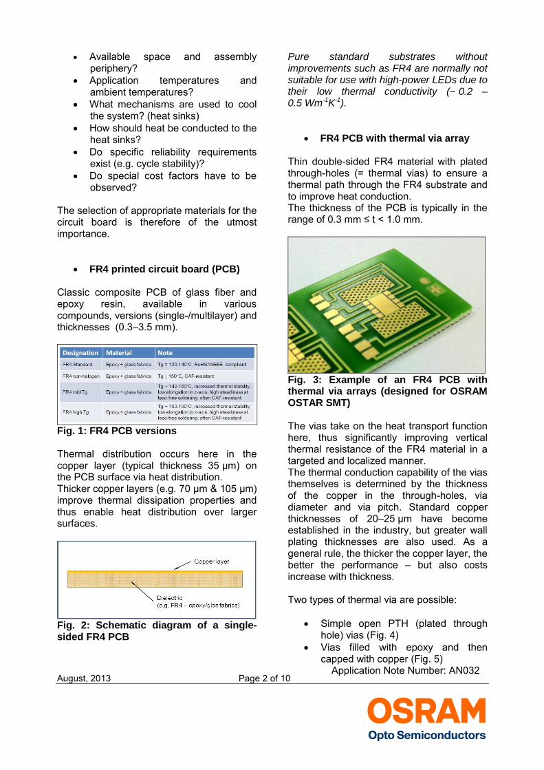
FR4 PCB with thermal via array Thin double-sided FR4 material with plated through-holes (= thermal vias) to ensure a thermal path through the FR4 substrate and to improve heat conduction. The thickness of the PCB is typically in the range of 0.3 mm ≤ t < 1.0 mm.
Fig. 3: Example of an FR4 PCB with thermal via arrays (designed for OSRAM OSTAR SMT) The vias take on the heat transport function here, thus significantly improving vertical thermal resistance of the FR4 material in a targeted and localized manner. The thermal conduction capability of the vias themselves is determined by the thickness of the copper in the through-holes, via diameter and via pitch. Standard copper thicknesses of 20–25 µm have become established in the industry, but greater wall plating thicknesses are also used. As a general rule, the thicker the copper layer, the better the performance – but also costs increase with thickness. Two types of thermal via are possible:
Simple open PTH (plated through hole) vias (Fig. 4)
Vias filled with epoxy and then capped with copper (Fig. 5)
Application Note Number: AN032

August, 2013 Page 3 of 10
Fig. 4: Schematic layout of a thermal via The use of thermally conductive silver pastes for filling to improve the thermal conductivity of the vias has in practice only a minor thermal effect but increases costs. For economic reasons it is thus better to slightly enlarge the copper thickness in the hole.
Fig 5: Schematic diagram of an OSLON LED on an FR4 PCB with plugged & filled vias The filled, copper-capped vias have the important advantage that they can be arranged directly under the thermal solder pad of the LED (e.g. OSLON, Golden DRAGON, OSLON Black Flat, etc.), meaning they are able to directly conduct heat. The copper plugging prevents uncontrolled solder wicking / solder voiding during reflow soldering at open vias (solder run-off).
Fig. 6: Unfilled thermal vias have solder wicking if used in solder pads
Uncontrolled solder wicking generates solder balls on the backside of the PCB (Fig.6), leading to insufficient thermal connection between the PCB and the heat sink. In many cases however, simple thermal vias are sufficient to achieve a clear reduction in thermal resistance down to the targeted value. The level of resultant thermal resistance is affected by the number and position of the vias. The closer the vias are located to the heat source, the better and more quickly can heat be dissipated and the lower the thermal resistance (Fig. 7).
Fig 7: Comparison of the effect of two different configurations of thermal vias (simulation) As a general rule it is advisable to design the copper surface around the solder pads, especially at the thermal pad if existing, to be as large as possible in order to achieve sufficient heat distribution across the FR4.
Thick copper PCB are PCBs with copper layer thicknesses of 105 µm to 400 µm, and up to 500 µm in special cases. According to requirements and technology used, layers are applied in a planar way as external and/or internal layer. The basis material used is FR4 or a metal substrate (Al, Cu) with a dielectric. The primary application sector consists of applications with high power (high current) and for the cooling of components with large thermal power losses. Constructions are mainly multi-layer or double-sided PCBs.
Application Note Number: AN032

August, 2013 Page 4 of 10
Fig. 8: Schematic diagram of a copper thick-layer PCB A special form is the so-called "iceberg" technology. Here a thin-layer copper layout is combined with selectively applied thick copper layers. The thick layer areas are recessed into the basis material (FR4) to achieve a uniform surface level. Expanding the copper cross-section achieves significantly wider heat dissipation as well as enabling local thermal build-up to be controlled.
Integrated copper wires and profiles
The base materials of FR4 technology are used here, in which application-specific copper wires and/or copper profiles are integrated and connected to the connection surfaces.
Fig. 9: Schematic PCB diagram with integrated copper wire/profile
Expansion of the copper cross-section favors thermal distribution, and heat can be specifically dissipated due to the individual position in the PCB. Typical copper cross-sections are for example: 2000 µm x 500 µm, 4000 µm x 500 µm
Insulated Metal Substrate (IMS) Insulated metal substrate (IMS) is the term for a PCB constructed with a metallic support plate separated by a thin dielectric from the copper conductors of the circuit. Aluminum is usually used as a carrier material because of low costs, and copper is also used with higher power densities because of its superior thermal conductivity. The attached dielectric has significant influence on total performance and is the determining factor for thermal resistance. Layers of unfilled and filled epoxy resins are used. With filled resins, 3 to 10-fold higher thermal conductivity is achieved compared to FR4 depending on filling material and quantity, but filling materials influence the cycle resistance of the board. Layer thickness of the dielectric is in the range of 20 µm to 100 µm, although the fact that decreasing thickness of the layer usually leads to a reduction of electrical dielectric strength must generally be taken into account. However, based on the structure, the IMS is mostly single-layer. Multi-layer versions are available but with higher costs.
Fig. 10: Typical layer construction of an insulated metal substrate PCB
Application Note Number: AN032

August, 2013 Page 5 of 10
In most applications IMS boards are attached to the heat sink together with a thermal interface material (TIM) by screws. When using an IMS-PCB with ceramic-based LEDs, it should be considered that the difference in the coefficients of thermal expansion (CTE) between the ceramic material of the LED and the IMS PCB creates stress on the solder joint. To minimize this effect, copper (Cu) is therefore preferred to aluminum (Al) as base plate material because of its lower CTE. Due to its significant higher thermal conductivity compared to FR4 technology (~ factor 10), IMS is widely-used in LED applications, especially with high power LEDs. In terms of material prices, costs with IMS can be approximately 2 to 4 times higher than with FR4.
IMS with Exposed Copper This is an optimized variant of IMS PCBs where the metal of the metal plate partially protrudes through the insulation layer (Exposed Cu). The housing is partly directly connected to the metallic carrier here for bridging the dielectric.
Fig. 11: LED on PCB with exposed copper Here heat can be dissipated without requiring any insulation between the thermal pad, the metal layer and the heat sink. This permits LEDs to be operated at higher currents or higher power levels for example.
It should be generally considered here that the connected thermal contact points are electrically neutral. In combination with ceramic based packages however, some PCB designs with exposed copper may cause higher thermal mechanical stresses during the assembly process. Because of this, application designs need to be verified to avoid damage. Please confer with application team of OSRAM Opto Semiconductors.
Aluminum with thin insulation layer
This is a modified form of IMS technology. Instead of a dielectric made of epoxy resin, a thin aluminum oxide or ceramic layer is used. Depending on the required dielectric strength, the dielectric layer thickness is in the range of <40µm to 125µm, whereby thermal conductivity of approximately 2W/mK is achieved.
Fig. 12: Schematic PCB diagram of aluminum with thin insulation layer
Thick/thin film ceramics
The core of the PCB here is a ceramic carrier substrate to which the conductors are directly applied via thick film or thin film technology. According to the specific variant, ceramic carriers have thicknesses of 0.25 mm to 3 mm. Because ceramic substrates themselves are electrically insulating but are thermally conductive, heat can be dissipated directly without other thermal barriers. Aluminum oxide and aluminum nitride are usually used as substrate materials, the latter having significantly superior thermal conductivity properties. The thermal conductivity of aluminum oxide is in the Application Note Number: AN032

August, 2013 Page 6 of 10
range of ~ 20 – 25 Wm-1K-1 , and that of aluminum nitride is at (~ 170 Wm-1K-1). Another advantage among many is low thermal expansion. In combination with ceramic-based High-Power LEDs, they are thus primarily suitable for applications with high thermal cyclic loads. With regard to thermal management, ceramic PCBs are generally very effective, but are often seen as a luxury variant because of their higher costs.
PCB Pad Finishes In general, all finishes are well-proven for SMT assembly, but with smaller solder pads the quality of the plating/finish is more important. Hot Air Solder Leveling (HAL/HASL) finish is less preferred for assembly because of the uneven surface compared to completely "flat" platings such as Cu-OSP (OSP: Organic Solderability Preservative) or immersion Sn or NiAu (ENIG). From a package point of view, it is difficult to recommend a particular PCB pad finish that will always meet all requirements. The choice of finish also depends strongly on board design, pad geometry, needs of other components on the board and process conditions, and must be chosen according to the needs of the specific application. Internal tests at OSRAM Opto Semiconductor have shown that Cu-OSP or NiAu are suitable and reliable platings in most cases.
Fig. 13: Comparison of PCB finishes
Application Note Number: AN032

August, 2013 Page 7 of 10
Second Level Reliability The term "second level reliability" usually appears in connection with the requirements and characteristics of the application or of the overall system (Fig. 14). It ultimately however refers to the reliability of the solder connection between the component (e.g. LED) and the printed circuit board (PCB) or carrier substrate.
Fig. 14: Requirements and properties for efficient system design The reliability of the soldered joint itself is determined or influenced by various factors, e.g. component housing, solder, mounting and soldering process and printed circuit board (Fig. 15).
This influence can take place either directly at the system development stage, e.g. an unsuitable combination of SMD package and PCB material (CTE mismatch), or when the individual components are processed, e.g. misalignment due to insufficient accuracy in assembly. Especially for LEDs with ceramic carrier substrate the aspect of second board reliability should therefore be considered when selecting the PCB type, or the possible effects should be considered. Thermal comparison of PCBs Based on data from the high-power LED OSRAM OSTAR Compact and a predefined heat sink, an exemplary thermal comparison of specific PCB concepts was carried out via thermal simulation. Typical key data and material parameters were used for the various PCB concepts. Figure 16 shows the principal construction and peripheral condition for the simulation as well as results for the individual PCB variants. The parameter for comparison was the resulting junction temperature TJ of the LED. The comparison was carried out exclusively according to thermal factors, and did not consider aspects of 2nd Board Reliability or other application-related requirements.
Fig. 15: Influencing factors on 2nd Board Reliability
Application Note Number: AN032

August, 2013 Page 8 of 10
If only the resultant junction temperature is considered, then all lie below the maximum permissible temperature level of 150 °C, related to the 25 °C ambient temperature. They are thus fundamentally suitable according to the specified conditions, but have differing optimization potential with regard to additional requirements or higher performance classes with the LEDs.
In summary, all PCB types have their advantages, and which type is best depends on the respective application in terms of individual requirements and conditions. Since PCB design, construction and material are essential for optimized thermal design, verification of the total system is therefore recommended.
Fig. 16: Thermal comparison of different PCB concepts Application Note Number: AN032

August, 2013 Page 9 of 10
Conclusion Many PCB technologies available on the market, along with their individual benefits and disadvantages, are suitable for LED applications. Because of good thermal distribution and mechanical stability, IMS technology with improved dielectrics is often given preference for many LED applications, especially for higher performance classes. In the mid-level to higher performance ranges, a focus is placed on FR4 technology with thermally optimized layouts. With simple measures such as supplementary copper surfaces, higher copper densities and thermal vias, the total system can be influenced at relatively low cost.
Nevertheless, all PCB types have their benefits, and which is best depends on the respective application with individual requirements and conditions. Since PCB design, construction and material are essential for optimized thermal designs, it is therefore recommended to verify the total system. OSRAM OPTO Semiconductors is able to support its customers during their development and design processes in finding the best solution for their specific applications. Further information regarding thermal management, processing and specific LED types etc. can be found on the OSRAM Opto Semiconductor website in the "Application Notes" section.
Appendix
Don't forget: ledlightforyou.com is the place to go whenever you need information and a list of worldwide partners for your LED lighting projects:
www.ledlightforyou.com Authors: Andreas Stich, Rainer Huber, Kurt-Jürgen Lang
Application Note Number: AN032

August, 2013 Page 10 of 10
ABOUT OSRAM OPTO SEMICONDUCTORS OSRAM, Munich, Germany is one of the two leading light manufacturers in the world. Its subsidiary, OSRAM Opto Semiconductors GmbH in Regensburg (Germany), offers its customers solutions based on semiconductor technology for lighting, sensor and visualization applications. Osram Opto Semiconductors has production sites in Regensburg (Germany), Penang (Malaysia) and Wuxi (China). Its headquarters for North America is in Sunnyvale (USA), and for Asia in Hong Kong. Osram Opto Semiconductors also has sales offices throughout the world. For more information go to www.osram-os.com. DISCLAIMER PLEASE CAREFULLY READ THE BELOW TERMS AND CONDITIONS BEFORE USING THE INFORMATION SHOWN HEREIN. IF YOU DO NOT AGREE WITH ANY OF THESE TERMS AND CONDITIONS, DO NOT USE THE INFORMATION. The information shown in this document is provided by OSRAM Opto Semiconductors GmbH on an “as is basis” and without OSRAM Opto Semiconductors GmbH assuming, express or implied, any warranty or liability whatsoever, including, but not limited to the warranties of correctness, completeness, merchantability, fitness for a particular purpose, title or non-infringement of rights. In no event shall OSRAM Opto Semiconductors GmbH be liable - regardless of the legal theory - for any direct, indirect, special, incidental, exemplary, consequential, or punitive damages related to the use of the information. This limitation shall apply even if OSRAM Opto Semiconductors GmbH has been advised of possible damages. As some jurisdictions do not allow the exclusion of certain warranties or limitations of liability, the above limitations or exclusions might not apply. The liability of OSRAM Opto Semiconductors GmbH would in such case be limited to the greatest extent permitted by law. OSRAM Opto Semiconductors GmbH may change the information shown herein at anytime without notice to users and is not obligated to provide any maintenance (including updates or notifications upon changes) or support related to the information. Any rights not expressly granted herein are reserved. Except for the right to use the information shown herein, no other rights are granted nor shall any obligation be implied requiring the grant of further rights. Any and all rights or licenses for or regarding patents or patent applications are expressly excluded.
Application Note Number: AN032