Embed Size (px)
Citation preview

PCB Stackup Design Considerationsfor Intel® FPGAsAN-6132017.06.28
SubscribeSend Feedback
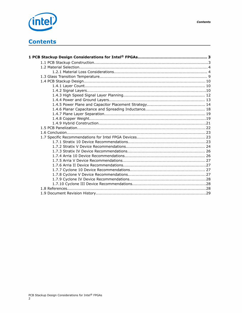
Contents
1 PCB Stackup Design Considerations for Intel® FPGAs...................................................... 31.1 PCB Stackup Construction........................................................................................31.2 Material Selection................................................................................................... 4
1.2.1 Material Loss Considerations........................................................................ 41.3 Glass Transition Temperature................................................................................... 91.4 PCB Stackup Design.............................................................................................. 10
1.4.1 Layer Count............................................................................................. 101.4.2 Signal Layers............................................................................................101.4.3 High Speed Signal Layer Planning............................................................... 121.4.4 Power and Ground Layers.......................................................................... 131.4.5 Power Plane and Capacitor Placement Strategy............................................. 141.4.6 Planar Capacitance and Spreading Inductance.............................................. 181.4.7 Plane Layer Separation.............................................................................. 191.4.8 Copper Weight..........................................................................................191.4.9 Hybrid Construction...................................................................................21
1.5 PCB Panelization................................................................................................... 221.6 Conclusion........................................................................................................... 231.7 Specific Recommendations for Intel FPGA Devices..................................................... 23
1.7.1 Stratix 10 Device Recommendations............................................................231.7.2 Stratix V Device Recommendations............................................................. 241.7.3 Stratix IV Device Recommendations............................................................ 261.7.4 Arria 10 Device Recommendations.............................................................. 261.7.5 Arria V Device Recommendations................................................................ 271.7.6 Arria II Device Recommendations................................................................271.7.7 Cyclone 10 Device Recommendations.......................................................... 271.7.8 Cyclone V Device Recommendations............................................................271.7.9 Cyclone IV Device Recommendations...........................................................281.7.10 Cyclone III Device Recommendations.........................................................28
1.8 References...........................................................................................................281.9 Document Revision History.....................................................................................29
Contents
PCB Stackup Design Considerations for Intel® FPGAs2
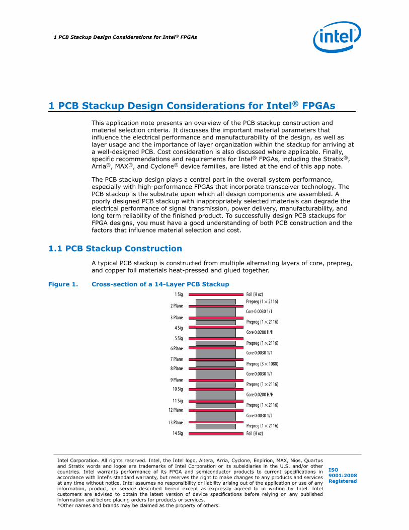
1 PCB Stackup Design Considerations for Intel® FPGAsThis application note presents an overview of the PCB stackup construction andmaterial selection criteria. It discusses the important material parameters thatinfluence the electrical performance and manufacturability of the design, as well aslayer usage and the importance of layer organization within the stackup for arriving ata well-designed PCB. Cost consideration is also discussed where applicable. Finally,specific recommendations and requirements for Intel® FPGAs, including the Stratix®,Arria®, MAX®, and Cyclone® device families, are listed at the end of this app note.
The PCB stackup design plays a central part in the overall system performance,especially with high-performance FPGAs that incorporate transceiver technology. ThePCB stackup is the substrate upon which all design components are assembled. Apoorly designed PCB stackup with inappropriately selected materials can degrade theelectrical performance of signal transmission, power delivery, manufacturability, andlong term reliability of the finished product. To successfully design PCB stackups forFPGA designs, you must have a good understanding of both PCB construction and thefactors that influence material selection and cost.
1.1 PCB Stackup Construction
A typical PCB stackup is constructed from multiple alternating layers of core, prepreg,and copper foil materials heat-pressed and glued together.
Figure 1. Cross-section of a 14-Layer PCB Stackup1 Sig
Core 0.0030 1/1
Prepreg (1 × 2116)
Prepreg (1 × 2116)
Core 0.0200 H/H
Prepreg (1 × 2116)
Core 0.0030 1/1
Prepreg (3 × 1080)
Core 0.0030 1/1
Prepreg (1 × 2116)
Core 0.0030 1/1
Prepreg (1 × 2116)
Prepreg (1 × 2116)
Core 0.0200 H/H
14 Sig
2 Plane
3 Plane
4 Sig
5 Sig
6 Plane
7 Plane
8 Plane
9 Plane
10 Sig
11 Sig
12 Plane
13 Plane
Foil (H oz)
Foil (H oz)
1 PCB Stackup Design Considerations for Intel® FPGAs
Intel Corporation. All rights reserved. Intel, the Intel logo, Altera, Arria, Cyclone, Enpirion, MAX, Nios, Quartusand Stratix words and logos are trademarks of Intel Corporation or its subsidiaries in the U.S. and/or othercountries. Intel warrants performance of its FPGA and semiconductor products to current specifications inaccordance with Intel's standard warranty, but reserves the right to make changes to any products and servicesat any time without notice. Intel assumes no responsibility or liability arising out of the application or use of anyinformation, product, or service described herein except as expressly agreed to in writing by Intel. Intelcustomers are advised to obtain the latest version of device specifications before relying on any publishedinformation and before placing orders for products or services.*Other names and brands may be claimed as the property of others.
ISO9001:2008Registered
The PCB manufacturer purchases the core material as a thin dielectric with copper cladfoils bonded to both sides. The core’s dielectric is a cured (hardened) fiberglass-weavematerial with epoxy resin that acts as an insulation layer between the copper foils. Forcore materials, the foils form the internal copper layers (signal or plane) in the PCB.Prepreg is an uncured fiberglass-epoxy resin weave that acts as the insulationbetween core layers and is the gluing agent for the cores. During the PCBmanufacturing process, multiple core and prepreg layers are combined with a top andbottom copper foil sheet. The combined layers are heat-pressed together to build thecomplete PCB stackup. The heat-press treatment cures the prepreg and binds all thedifferent layers together to form the PCB.
1.2 Material Selection
The complex FPGA boards that incorporate the Stratix 10 device families of transceivertechnologies require higher layer counts as well as lower loss materials to run at up to56 Gbps. High layer count facilitates the high density signal break-out, routing, andpower distribution, while the high-performance low-loss material is required tosuccessfully transmit and receive 10 Gbps+ transceiver data rates over extendedbackplane channel lengths. High layer count PCBs often suffer from lamination anddrilling challenges in the PCB manufacturing process. Together with low-loss materials,they put added cost pressure on the system designer. To meet these challenges,designers must understand the material properties that influence signal loss and PCBmanufacturability in order to properly select the best performance material at thelowest cost for a successful and robust design.
1.2.1 Material Loss Considerations
At low data rates, signal loss is caused mainly by impedance mismatches and less soby dielectric absorption and conductor losses from the material. Impedance mismatchis well understood by design engineers who regularly specify controlled impedancetraces by tightly managing trace geometries, separation, and routes during the layoutdesign. However, at data rates of 10 Gbps and above, material loss becomes veryimportant and controlled dielectric construction must be considered during the designprocess. To mitigate loss caused by the material, the following material parametersmust be considered during the material selection process:
• Relative Dielectric Constant
• Loss Tangent
• Fiberglass Weave Composition
• Skin Effect
These material parameters have significant impact on the electrical properties.Therefore, you should consider them as critical parameters during the stackup design.
Related Links
• Relative Dielectric Constant on page 5
• Loss Tangent on page 5
• Fiberglass Weave Composition on page 7
• Skin Effect on page 8
1 PCB Stackup Design Considerations for Intel® FPGAs
PCB Stackup Design Considerations for Intel® FPGAs4
1.2.1.1 Relative Dielectric Constant
The relative dielectric constant (εr) is a measure of a material’s ability to be polarizedby an electric field and store electrostatic energy, as well as its ability to facilitatesignal propagation. The relative dielectric constant varies with frequency. Materialdatasheets often refer to this parameter as Dk. Low εr or Dk materials make excellentinsulators and are good for isolating signals on adjacent layers.
From a board designer’s perspective, the benefits of a lower dielectric constant includethe following:
• Better insulation
• Faster signal propagation through the material
• Higher trace impedance for a given trace geometry
• Smaller stray trace capacitance
PCB manufacturers typically characterize εr at 1 MHz. However, the dielectric constantof a material is generally a function of its frequency. As frequency increases, εr isreduced. Because of this non-uniformity, a transmission line’s impedance can varyfrom its calculated value at 1 MHz, causing it to differ from what a propagating signalactually sees on the channel. As board designer, you should get the Dk value at highfrequency range for using the high data rates signal on the board.
Because digital signals are comprised of many frequencies (harmonics), the resultingdifference in impedance that is presented to the different harmonics can cause signalloss from both reflections and phase distortion (phase jitter) arising from the differentharmonics arriving at the destination at different times.
Always choose lower εr material with a flat frequency response whenever possible forbest signal performance and to minimize signal distortion and phase jitter.
1.2.1.2 Loss Tangent
Loss tangent (tan(δ)) is a measure of signal loss as the signal propagates down thetransmission line. Material datasheets and PCB manufacturers commonly refer to thissignal loss as the dissipation factor (Df). tan(δ) or Df is the result of electromagneticwave absorption by the dielectric material and depends on the material’s structure andglass-resin composition. A lower loss tangent results in more of the originaltransmitted signal getting through to its destination. This is important for transceiver-based designs where multi-gigabit signals must be transmitted across long backplanechannels. A large loss tangent means more dielectric absorption and less of thetransmitted signal is getting through to its destination. Below equation shows thesignal attenuation due to the loss tangent, measured in decibels per inch (dB/in).Attenuation = 2.3 * f * tan δ * εr
Where:
• f is the frequency in GHz
• tan(δ) is the dimensionless loss tangent
• εr is the relative dielectric constant of the material
Ideally, selecting the lowest loss material is the best choice. However, lower losscomes at an increased cost tradeoff. A better approach is to plot attenuation equationagainst frequency for the various material choices under consideration and compare
1 PCB Stackup Design Considerations for Intel® FPGAs
PCB Stackup Design Considerations for Intel® FPGAs5
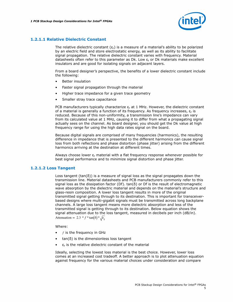
the signal attenuation for the target data rate and reach required. For example, belowfigure shows this attenuation for some common PCB materials by plotting attenuationequation against frequency up to 20 GHz.
Figure 2. Comparison of Loss Tangent Attenuation
Table 1. Material Dielectric Constant and Loss TangentBelow table lists the εr and tan(δ) of each material plotted in above figure.
Material εr tan(δ)
Typical FR4 4 0.02
GETEK 3.9 0.01
Isola 370HR 4.17 0.016
Isola FR406 4.29 0.014
Isola FR408 3.70 0.011
Panasonic Megtron 6 3.4 0.002
Nelco 4000-6 4.12 0.012
Nelco 4000-13 EP 3.7 0.009
Nelco 4000-13 EP SI 3.2 0.008
Rogers 4350B 3.48 0.0037
For example, suppose a design running at 10 Gbps requiring a maximum reach of 40inches is targeted for the Nelco 4000-13 EP material. Because the Nyquist frequency is5 GHz for a 10 Gbps data rate, the resulting loss that is due solely to the dielectricabsorption of Nelco 4000-13EP material is 0.2 dB per inch multiplied by 40 inches oftrace length, resulting in 8 dB of signal attenuation just from the material dielectric
1 PCB Stackup Design Considerations for Intel® FPGAs
PCB Stackup Design Considerations for Intel® FPGAs6
absorption. Next, suppose a maximum total loss budget of 10 dB is required for asignal to be properly recovered at the receiver. In this case, most of the signal loss isalready consumed by the material dielectric, so a lower loss material or shorter reachmust be considered, because additional conductor losses are expected from tracediscontinuities, skin effect, vias, and connector assemblies that may be present in thetransmission path.
Furthermore, as an example of material cost considerations, below table lists anapproximate normalized cost factor relationship for some common PCB materialsrelative to FR4. Because material costs can vary depending on the PCB vendor, consultthe PCB vendor for their latest pricing and relative cost factor data when deciding onmaterial performance versus cost tradeoffs.
Table 2. Normalized Material Cost Comparison
Material Group Vendor Specific FR4 Relative Cost Factor
170 Tg FR4 (Baseline) Nelco 4000-6 1
High Tg / Reliability-Filled Isola 370HR 1.1
High Speed / Low Loss Isola FR408 1.8
High Speed / Low Loss Nelco 4000-13 EP 2.1
High Speed / Very Low Loss Nelco 4000-13 EP SI 3.2
High Frequency Arlon 85N 4
High Frequency IS680-3.45 4.2
High Speed / Very Low Loss Panasonic Megtron 6 5
High Frequency Rogers 4350B 5.6
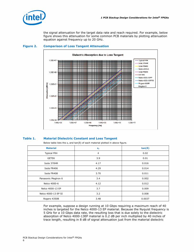
1.2.1.3 Fiberglass Weave Composition
The fiberglass within the core and prepreg is constructed by weaving fibers of glassyarn together to form fabric-like fiberglass sheets. These sheets are then impregnatedwith an epoxy resin to form the core (cured resin) and prepreg (uncured resin)materials. Because the glass yarn comes in different densities and thicknesses, theresulting sheets can range from loosely-weaved to tightly-weaved fiberglass-epoxy fill.
Figure 3. Different Styles of Fibreglss Weaves
The fiberglass weaves are typically classified into different glass styles, based on theyarn count and the type of fiberglass yarn used, as listed in below table.
1 PCB Stackup Design Considerations for Intel® FPGAs
PCB Stackup Design Considerations for Intel® FPGAs7
Table 3. Common Fibreglass Weave Styles
Glass Style Count Warp Count per Inch Warp Yarn Yarn Fill Glass Thickness
106 56 56 ECD-900 1/0 ECD-900 1/0 0.0015
1080 60 47 ECD-450 1/0 ECD-450 1/0 0.0025
1280 60 60 ECD-450 1/0 ECD-450 1/0 0.0022
2113 60 56 ECE-225 1/0 ECD-450 1/0 0.0029
2116 60 58 ECE-225 1/0 ECE-225 1/0 0.0038
3070 70 70 ECDE-300 1/0 ECDE-300 1/0 0.0034
1652 52 52 ECG-150 1/0 ECG-150 1/0 0.0045
7628 44 31 ECG-75 1/0 ECG-75 1/0 0.0068
The tighter the weave netting, the more uniform the dielectric constant. Loose weavesresulting in less uniform dielectric constants in the PCB laminate can cause traceimpedance variations and propagation skews in tightly matched signals, such asdifferential pairs that directly reference the weave. For example, on a sparse weavingsuch as glass style 106, one leg of the differential pair may be routed directly over afiber weave while the other leg is routed between the fiber weaves. This results in adifferent εr for each leg of the differential channel.
In general, to counteract this skew, route traces at a small angle in a zig-zag fashionrelative to the fiberglass strands to average out the number of on-weave and off-weave traces. This technique requires more board routing room and may not beachievable in a space-constrained board. In this situation, select a more tightly wovenglass style for the dielectric surrounding the high speed trace layers. Because moretightly woven glass styles add cost to the PCB, a good compromise is to select amedium woven glass style such as 2116 for the high-speed trace layers and a lower-cost 106 or 1080 glass style for other lower-speed signal layers.
For board design with ultra-high speed transceiver signals, Intel recommends tochoose spread glass materials to mitigate this effect.
Related Links
AN 528: PCB Dielectric Material Selection and Fiber Weave Effect on High-SpeedChannel
1.2.1.4 Skin Effect
In addition to dielectric absorption, signal attenuation can also occur because ofresistive losses from the channel. Channel resistance is a function of frequency. Forlow frequencies, you can calculate the DC channel resistance from below equation.
DC Channel Resistance
RDC = ρ −A
L
Where:
1 PCB Stackup Design Considerations for Intel® FPGAs
PCB Stackup Design Considerations for Intel® FPGAs8
• RDC is the DC channel resistance in ohms (Ω)
• ρ is the resistivity of copper 6.787x10⁻⁷ ohm-in)
• L is the trace length in inches
• A is the cross-sectional area of the trace in square inches
However, as the frequency increases, the resistive channel loss increases becausecurrent flows toward the surface of the copper trace. The surface penetration of thiscurrent flow is referred to as the skin depth (δ). This skin effect reduces the cross-sectional area of the channel, increasing the channel resistance. Countering this effecttypically requires widening the trace width to increase the effective surface area.Increasing the copper weight of the traces does little, because most of the current islimited by the skin depth. The extent of trace width required usually entails calculatingthe skin depth.
Skin Depth
δ = 2.598 * 10−3 1f
Where:
• δ is skin depth in inches
• f is frequency in MHz
Channel Resistance for a Copper TraceRAC = ρ L
W * δ
Where:
• RAC is the frequency dependent channel resistance for a copper trace
• ρ is the resistivity of copper (6.787x10⁻⁷ ohm-in)
• L is the trace length in inches
• δ is skin depth in inches
• W is the trace width in inches
Based on the results of the skin depth and channel resistance, signal traces must besized appropriately to reduce resistive losses because of the skin effect.
1.3 Glass Transition Temperature
In addition to material loss contributions, the manufacturability of the PCB must alsobe considered. One parameter that can impact PCB manufacturability is the glasstransition temperature (Tg).
All materials are subject to expansion and contraction as a result of temperaturechanges. The rate of expansion and contraction is determined by the material’scoefficient of thermal expansion (CTE). The glass transition temperature (Tg) is theknee point temperature at which the resin in the material begins to expand muchfaster than the expansion of the surrounding glass weave and copper. Ideally, theresin, glass, and copper in the PCB all have similar temperature coefficients so allthree materials expand and contract together at a similar rate. However, attemperatures beyond Tg, the faster expansion of the resin increases the mechanicalstress on the PCB structure. Because the copper and glass-weave are laminated
1 PCB Stackup Design Considerations for Intel® FPGAs
PCB Stackup Design Considerations for Intel® FPGAs9
together, they reinforce the PCB in the lateral X and Y direction. The resultingexpansion is forced to take place mostly in the vertical Z direction. This rapid verticalexpansion can over-stress via structures resulting in via fractures and even PCBdelamination in severe cases if the expansion is excessive.
When choosing a material, ensure the Tg is high enough to withstand the expectedmanufacturing temperature cycles for both assembly and rework to ensure PCBmanufacturing reliability. For restriction of hazardous substance (RoHS) compliantprocesses, reflow temperatures can sustain 240° C and even peak at 260° C. Workwith the PCB manufacturer to ensure the selected material is appropriate for thetargeted manufacturing process.
1.4 PCB Stackup Design
The goal of any PCB stackup design is to select the material and specify the layerordering such that it adequately delivers the required signal performance and powerintegrity at the lowest PCB cost. After the appropriate PCB material is selected,consider the following issues to design the layer stackup.
1.4.1 Layer Count
The total number of layers required for a given design is dependent on the complexityof the board. These factors include the number of signal nets that must break outfrom the ball-grid array (BGA) device, the number of power planes or pours, and thecomponent density and type of packages for those components. Typically, large BGAdevice breakouts and individual power or ground plane requirements determine thefinal board layer count. For complex FPGA boards, the FPGA device in many cases isusually the largest BGA device on the board and thus determines the board’sminimum layer count.
1.4.2 Signal Layers
In high-density FPGAs, many signal layers are required to achieve full breakout of allavailable I/Os.
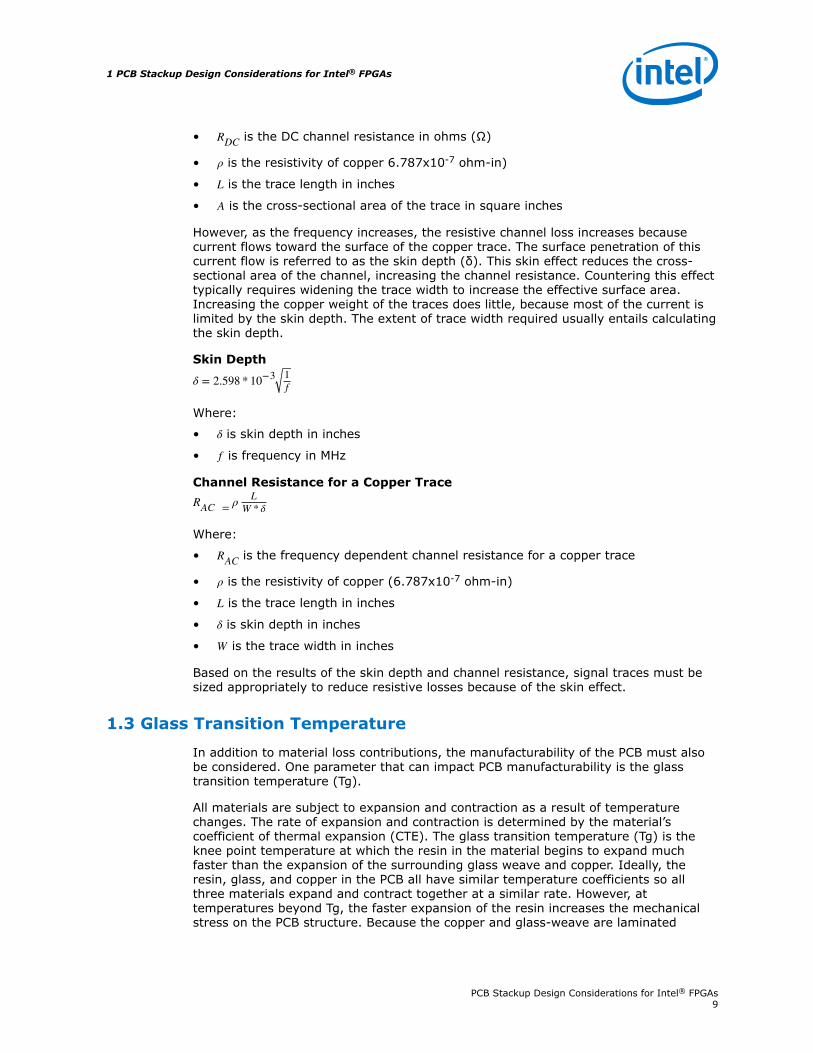
A good estimate for the minimum number of signal layers required is to count thedepth of the row or column I/O signal balls of the FPGA device, divide that number bytwo, and round up to the nearest even whole number.
For example, on a Stratix IV GX device in an F1517 BGA package, the I/O row andcolumn span 13 deep as shown in below figure. Therefore, a minimum of seven signallayers are required for a complete I/O signal breakout for that device. However, for abalanced PCB stackup, eight signals layers must be used.
1 PCB Stackup Design Considerations for Intel® FPGAs
PCB Stackup Design Considerations for Intel® FPGAs10
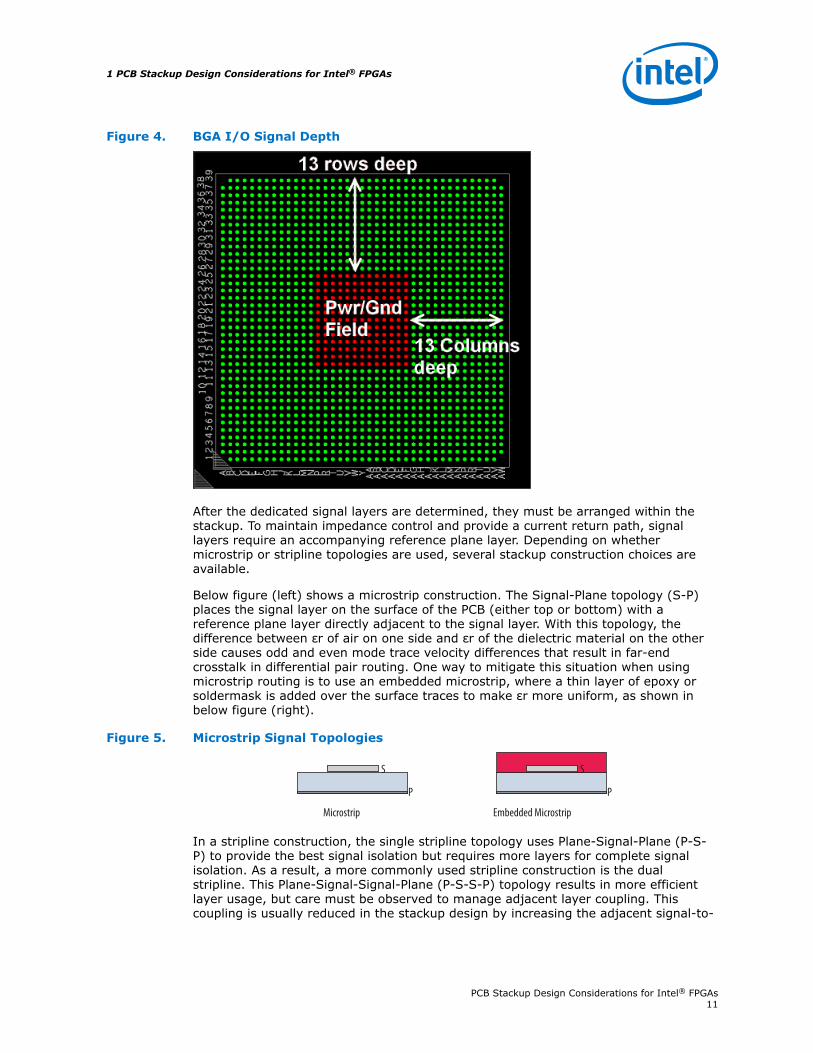
Figure 4. BGA I/O Signal Depth
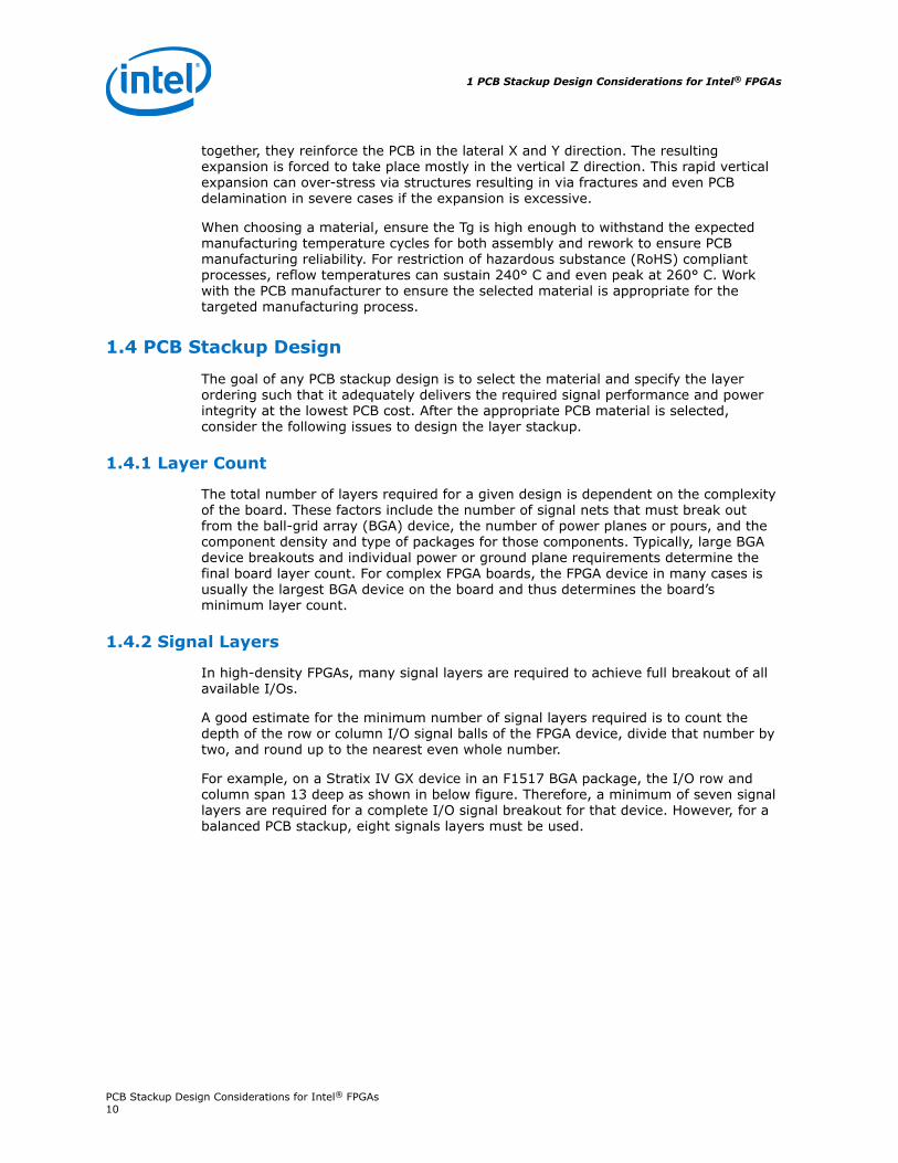
After the dedicated signal layers are determined, they must be arranged within thestackup. To maintain impedance control and provide a current return path, signallayers require an accompanying reference plane layer. Depending on whethermicrostrip or stripline topologies are used, several stackup construction choices areavailable.
Below figure (left) shows a microstrip construction. The Signal-Plane topology (S-P)places the signal layer on the surface of the PCB (either top or bottom) with areference plane layer directly adjacent to the signal layer. With this topology, thedifference between εr of air on one side and εr of the dielectric material on the otherside causes odd and even mode trace velocity differences that result in far-endcrosstalk in differential pair routing. One way to mitigate this situation when usingmicrostrip routing is to use an embedded microstrip, where a thin layer of epoxy orsoldermask is added over the surface traces to make εr more uniform, as shown inbelow figure (right).
Figure 5. Microstrip Signal Topologies
Embedded Microstrip
S
P
Microstrip
S
P
In a stripline construction, the single stripline topology uses Plane-Signal-Plane (P-S-P) to provide the best signal isolation but requires more layers for complete signalisolation. As a result, a more commonly used stripline construction is the dualstripline. This Plane-Signal-Signal-Plane (P-S-S-P) topology results in more efficientlayer usage, but care must be observed to manage adjacent layer coupling. Thiscoupling is usually reduced in the stackup design by increasing the adjacent signal-to-
1 PCB Stackup Design Considerations for Intel® FPGAs
PCB Stackup Design Considerations for Intel® FPGAs11
signal separation compared to the signal-to-plane separation. Doing this forces themajority of the return current along the reference plane layer directly above or belowthe signal instead of onto the adjacent signal layer. However, having large separationsadds to the overall thickness of the board. This can impact standard boardmanufacturing if the aspect ratio of the via drill to board thickness is larger than 10:1.In addition to layer separation, signal-to-signal coupling can also be minimized byrouting adjacent layers orthogonally to each other to minimize the overlappingcoupling region. An added benefit of stripline routing is zero far-end crosstalk becauseof a uniform εr surrounding the signal traces.
Figure 6. Stripline Signal Topologies
Single Stripline
S
P (PWR/GND)
P (PWR/GND)
Dual Stripline
S
S
P (PWR/GND)
P (PWR/GND)
1.4.3 High Speed Signal Layer Planning
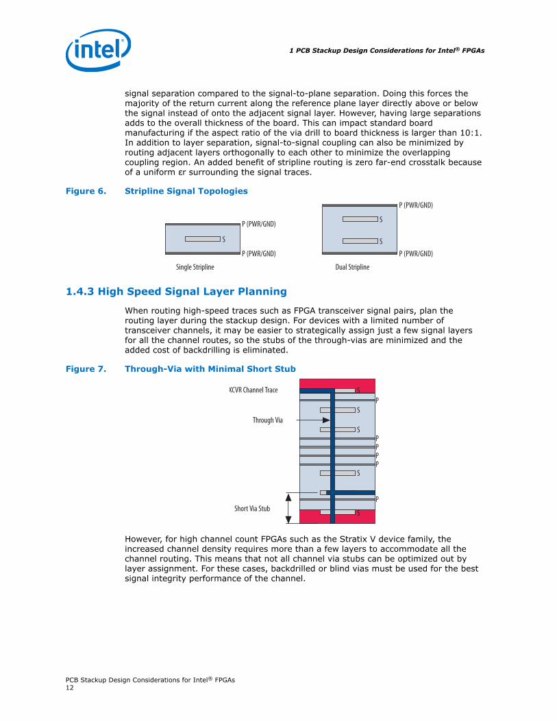
When routing high-speed traces such as FPGA transceiver signal pairs, plan therouting layer during the stackup design. For devices with a limited number oftransceiver channels, it may be easier to strategically assign just a few signal layersfor all the channel routes, so the stubs of the through-vias are minimized and theadded cost of backdrilling is eliminated.
Figure 7. Through-Via with Minimal Short Stub
Through Via
Short Via Stub
S
S
S
S
S
P
P
PPPP
XCVR Channel Trace
However, for high channel count FPGAs such as the Stratix V device family, theincreased channel density requires more than a few layers to accommodate all thechannel routing. This means that not all channel via stubs can be optimized out bylayer assignment. For these cases, backdrilled or blind vias must be used for the bestsignal integrity performance of the channel.
1 PCB Stackup Design Considerations for Intel® FPGAs
PCB Stackup Design Considerations for Intel® FPGAs12
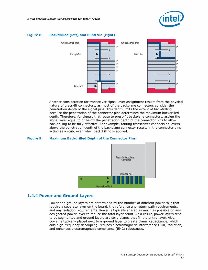
Figure 8. Backdrilled (left) and Blind Via (right)
Blind ViaS
S
S
S
S
S
P
PPPP
XCVR Channel Trace
Through Via
Back-Drill
S
S
S
S
S
P
P
PPPP
XCVR Channel TraceP
Another consideration for transceiver signal layer assignment results from the physicalnature of press-fit connectors, as most of the backplane connectors consider thepenetration depth of the signal pins. This depth limits the extent of backdrillingbecause the penetration of the connector pins determines the maximum backdrilleddepth. Therefore, for signals that route to press-fit backplane connectors, assign thesignal layer equal to or below the penetration depth of the connector pins to allowbackdrilling to be fully effective. For example, routing transceiver channels on layersabove the penetration depth of the backplane connector results in the connector pinsacting as a stub, even when backdrilling is applied.
Figure 9. Maximum Backdrilled Depth of the Connector Pins
Press-Fit BackplaneConnector
Connector Pins
Penetration Depth
PCB
1.4.4 Power and Ground Layers
Power and ground layers are determined by the number of different power rails thatrequire a separate layer on the board, the reference and return path requirements,and any isolation requirements. Power is typically shared as much as possible on anydesignated power layer to reduce the total layer count. As a result, power layers tendto be segmented and ground layers are solid planes that fill the entire layer. Also,power is typically placed next to a ground layer to create planar capacitance, whichaids high-frequency decoupling, reduces electromagnetic interference (EMI) radiation,and enhances electromagnetic compliance (EMC) robustness.
1 PCB Stackup Design Considerations for Intel® FPGAs
PCB Stackup Design Considerations for Intel® FPGAs13
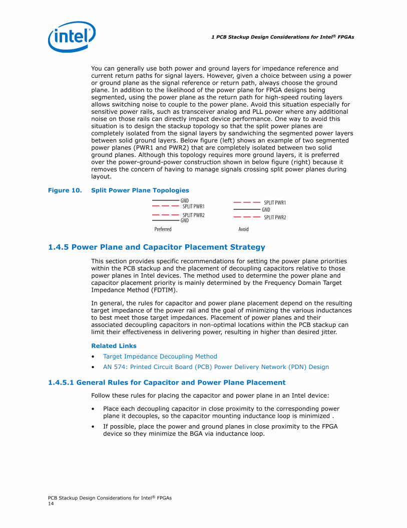
You can generally use both power and ground layers for impedance reference andcurrent return paths for signal layers. However, given a choice between using a poweror ground plane as the signal reference or return path, always choose the groundplane. In addition to the likelihood of the power plane for FPGA designs beingsegmented, using the power plane as the return path for high-speed routing layersallows switching noise to couple to the power plane. Avoid this situation especially forsensitive power rails, such as transceiver analog and PLL power where any additionalnoise on those rails can directly impact device performance. One way to avoid thissituation is to design the stackup topology so that the split power planes arecompletely isolated from the signal layers by sandwiching the segmented power layersbetween solid ground layers. Below figure (left) shows an example of two segmentedpower planes (PWR1 and PWR2) that are completely isolated between two solidground planes. Although this topology requires more ground layers, it is preferredover the power-ground-power construction shown in below figure (right) because itremoves the concern of having to manage signals crossing split power planes duringlayout.
Figure 10. Split Power Plane Topologies
Preferred
GND
GNDSPLIT PWR2SPLIT PWR1
Avoid
GNDSPLIT PWR2
SPLIT PWR1
1.4.5 Power Plane and Capacitor Placement Strategy
This section provides specific recommendations for setting the power plane prioritieswithin the PCB stackup and the placement of decoupling capacitors relative to thosepower planes in Intel devices. The method used to determine the power plane andcapacitor placement priority is mainly determined by the Frequency Domain TargetImpedance Method (FDTIM).
In general, the rules for capacitor and power plane placement depend on the resultingtarget impedance of the power rail and the goal of minimizing the various inductancesto best meet those target impedances. Placement of power planes and theirassociated decoupling capacitors in non-optimal locations within the PCB stackup canlimit their effectiveness in delivering power, resulting in higher than desired jitter.
Related Links
• Target Impedance Decoupling Method
• AN 574: Printed Circuit Board (PCB) Power Delivery Network (PDN) Design
1.4.5.1 General Rules for Capacitor and Power Plane Placement
Follow these rules for placing the capacitor and power plane in an Intel device:
• Place each decoupling capacitor in close proximity to the corresponding powerplane it decouples, so the capacitor mounting inductance loop is minimized .
• If possible, place the power and ground planes in close proximity to the FPGAdevice so they minimize the BGA via inductance loop.
1 PCB Stackup Design Considerations for Intel® FPGAs
PCB Stackup Design Considerations for Intel® FPGAs14
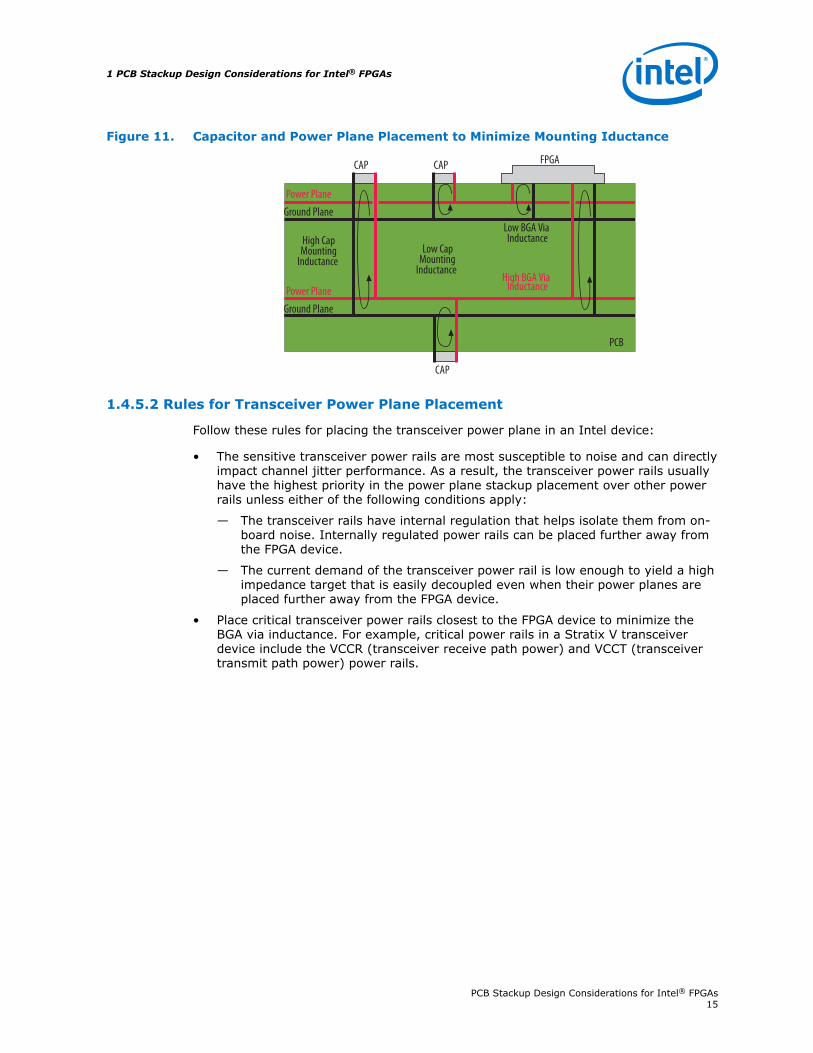
Figure 11. Capacitor and Power Plane Placement to Minimize Mounting Iductance
CAP CAP
CAP
PCB
FPGA
Power PlaneGround Plane
Power PlaneGround Plane
High CapMounting
Inductance
Low BGA ViaInductance
High BGA ViaInductance
Low CapMounting
Inductance
1.4.5.2 Rules for Transceiver Power Plane Placement
Follow these rules for placing the transceiver power plane in an Intel device:
• The sensitive transceiver power rails are most susceptible to noise and can directlyimpact channel jitter performance. As a result, the transceiver power rails usuallyhave the highest priority in the power plane stackup placement over other powerrails unless either of the following conditions apply:
— The transceiver rails have internal regulation that helps isolate them from on-board noise. Internally regulated power rails can be placed further away fromthe FPGA device.
— The current demand of the transceiver power rail is low enough to yield a highimpedance target that is easily decoupled even when their power planes areplaced further away from the FPGA device.
• Place critical transceiver power rails closest to the FPGA device to minimize theBGA via inductance. For example, critical power rails in a Stratix V transceiverdevice include the VCCR (transceiver receive path power) and VCCT (transceivertransmit path power) power rails.
1 PCB Stackup Design Considerations for Intel® FPGAs
PCB Stackup Design Considerations for Intel® FPGAs15
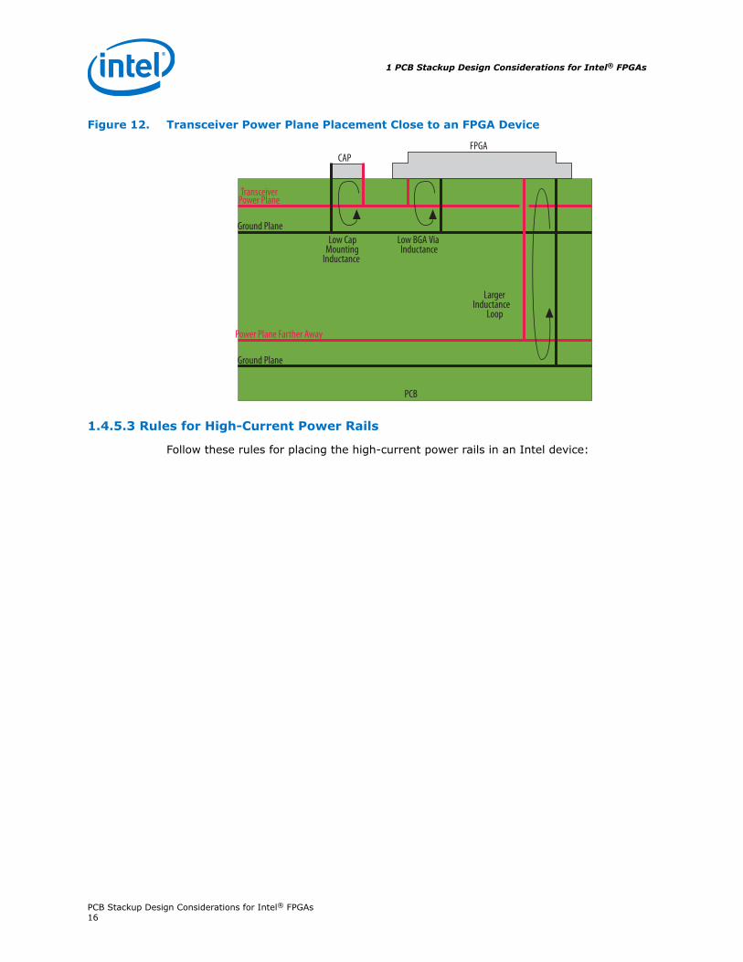
Figure 12. Transceiver Power Plane Placement Close to an FPGA Device
CAP
PCB
FPGA
Ground Plane
Ground Plane
Power Plane Farther Away
Transceiver Power Plane
LargerInductance
Loop
Low Cap Mounting
Inductance
Low BGA ViaInductance
1.4.5.3 Rules for High-Current Power Rails
Follow these rules for placing the high-current power rails in an Intel device:
1 PCB Stackup Design Considerations for Intel® FPGAs
PCB Stackup Design Considerations for Intel® FPGAs16
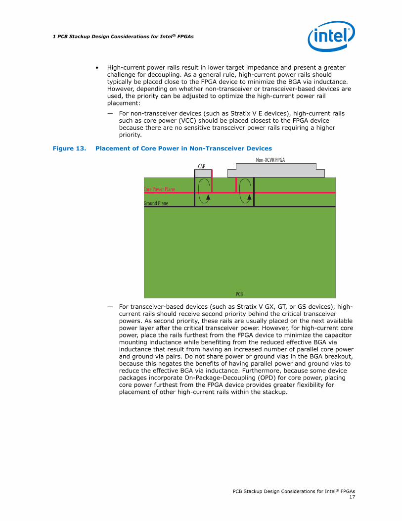
• High-current power rails result in lower target impedance and present a greaterchallenge for decoupling. As a general rule, high-current power rails shouldtypically be placed close to the FPGA device to minimize the BGA via inductance.However, depending on whether non-transceiver or transceiver-based devices areused, the priority can be adjusted to optimize the high-current power railplacement:
— For non-transceiver devices (such as Stratix V E devices), high-current railssuch as core power (VCC) should be placed closest to the FPGA devicebecause there are no sensitive transceiver power rails requiring a higherpriority.
Figure 13. Placement of Core Power in Non-Transceiver Devices
CAP
PCB
Non-XCVR FPGA
Ground Plane
Core Power Plane
— For transceiver-based devices (such as Stratix V GX, GT, or GS devices), high-current rails should receive second priority behind the critical transceiverpowers. As second priority, these rails are usually placed on the next availablepower layer after the critical transceiver power. However, for high-current corepower, place the rails furthest from the FPGA device to minimize the capacitormounting inductance while benefiting from the reduced effective BGA viainductance that result from having an increased number of parallel core powerand ground via pairs. Do not share power or ground vias in the BGA breakout,because this negates the benefits of having parallel power and ground vias toreduce the effective BGA via inductance. Furthermore, because some devicepackages incorporate On-Package-Decoupling (OPD) for core power, placingcore power furthest from the FPGA device provides greater flexibility forplacement of other high-current rails within the stackup.
1 PCB Stackup Design Considerations for Intel® FPGAs
PCB Stackup Design Considerations for Intel® FPGAs17
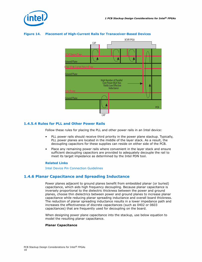
Figure 14. Placement of High-Current Rails for Transceiver-Based Devices
CAP
CAP
PCB
XCVR FPGA
Other High Current Power Plane
Ground Plane
Ground Plane
Ground Plane
Core Power
XCVR Power Plane
High Number of ParallelCore Power BGA ViasYields Low Effective
Inductance
1.4.5.4 Rules for PLL and Other Power Rails
Follow these rules for placing the PLL and other power rails in an Intel device:
• PLL power rails should receive third priority in the power plane stackup. Typically,PLL power planes are located in the middle of the layer stack. As a result, thedecoupling capacitors for these supplies can reside on either side of the PCB.
• Place any remaining power rails where convenient in the layer stack and ensuresufficient decoupling capacitors are provided to adequately decouple the rail tomeet its target impedance as determined by the Intel PDN tool.
Related Links
Intel Device Pin Connection Guidelines
1.4.6 Planar Capacitance and Spreading Inductance
Power planes adjacent to ground planes benefit from embedded planar (or buried)capacitance, which aids high frequency decoupling. Because planar capacitance isinversely proportional to the dielectric thickness between the power and groundplanes, choose thin dielectrics between power and ground planes to increase planarcapacitance while reducing planar spreading inductance and overall board thickness.The reduction of planar spreading inductance results in a lower impedance path andincreases the effectiveness of discrete capacitances (such as 0402 or 0603capacitances) that are frequently used for decoupling on the board.
When designing power plane capacitance into the stackup, use below equation tomodel the resulting planar capacitance.
Planar Capacitance
1 PCB Stackup Design Considerations for Intel® FPGAs
PCB Stackup Design Considerations for Intel® FPGAs18
C = εo * εr * Ah
Where:
• C is the capacitance
• εo is the permittivity of free space (8.85x10⁻¹² F/m)
• εr is the relative permittivity of the dielectric
• A is the area of overlap between the power and ground plane
• h is the dielectric separation between the planes
Use below equation to determine the planar spreading inductance of the power-groundplane sandwich.Ls = μo * h * l
w
Where:
• Ls is the planar spreading inductance
• μo is the permeability of free space (32 pH/mil)
• h,l, and w are the respective separation between the power-ground sandwich,length and width of the plane in mils
1.4.7 Plane Layer Separation
To benefit from the inherent planar capacitance associated with the different potentialplanes, make the power-to-ground layer separation as small as possible. Because thedielectric breakdown voltage (DBV) in all common PCB materials is generally 1000V/mil or higher, dielectric failure between power and ground planes is not a concernfor typical electronic applications where the voltage requirement is usually 12 V andlower. As a result, when designing planar capacitance, use the thinnest core dielectricavailable for the power-ground sandwich for the highest capacitance per planar area.
The thinnest standard core dielectric commonly used for the power-ground planarcapacitance without incurring a cost premium is typically 3 mils. For thinner cores,several manufacturers offer 2 mil core, 1 mil core, and even sub-1 mil corethicknesses at an additional cost. Consider the ZBC cores from vendors like Sanmina,FaradFlex cores from Oak Mitsui Technologies, or ECM (Embedded CapacitanceMaterial) cores from 3M Corporation for constructing even larger buried capacitancesper area within the PCB stackup.
1.4.8 Copper Weight
A copper foil is specified in terms of its weight in ounces per square foot (oz/ft2),although it is more commonly referred to in ounces (oz). Typical PCB copper weightsare 0.5 oz, 1 oz, and 2 oz. Below table lists the corresponding copper thicknesses forvarious copper weights.
1 PCB Stackup Design Considerations for Intel® FPGAs
PCB Stackup Design Considerations for Intel® FPGAs19
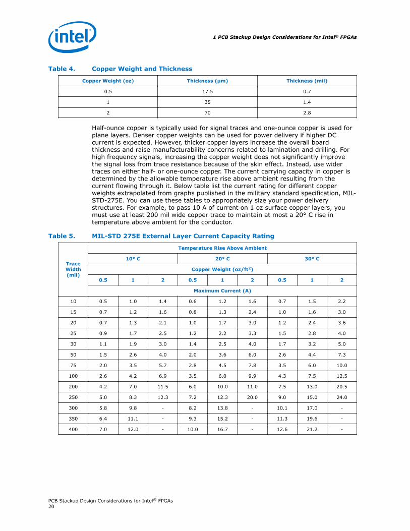
Table 4. Copper Weight and Thickness
Copper Weight (oz) Thickness (μm) Thickness (mil)
0.5 17.5 0.7
1 35 1.4
2 70 2.8
Half-ounce copper is typically used for signal traces and one-ounce copper is used forplane layers. Denser copper weights can be used for power delivery if higher DCcurrent is expected. However, thicker copper layers increase the overall boardthickness and raise manufacturability concerns related to lamination and drilling. Forhigh frequency signals, increasing the copper weight does not significantly improvethe signal loss from trace resistance because of the skin effect. Instead, use widertraces on either half- or one-ounce copper. The current carrying capacity in copper isdetermined by the allowable temperature rise above ambient resulting from thecurrent flowing through it. Below table list the current rating for different copperweights extrapolated from graphs published in the military standard specification, MIL-STD-275E. You can use these tables to appropriately size your power deliverystructures. For example, to pass 10 A of current on 1 oz surface copper layers, youmust use at least 200 mil wide copper trace to maintain at most a 20° C rise intemperature above ambient for the conductor.
Table 5. MIL-STD 275E External Layer Current Capacity Rating
TraceWidth(mil)
Temperature Rise Above Ambient
10° C 20° C 30° C
Copper Weight (oz/ft2)
0.5 1 2 0.5 1 2 0.5 1 2
Maximum Current (A)
10 0.5 1.0 1.4 0.6 1.2 1.6 0.7 1.5 2.2
15 0.7 1.2 1.6 0.8 1.3 2.4 1.0 1.6 3.0
20 0.7 1.3 2.1 1.0 1.7 3.0 1.2 2.4 3.6
25 0.9 1.7 2.5 1.2 2.2 3.3 1.5 2.8 4.0
30 1.1 1.9 3.0 1.4 2.5 4.0 1.7 3.2 5.0
50 1.5 2.6 4.0 2.0 3.6 6.0 2.6 4.4 7.3
75 2.0 3.5 5.7 2.8 4.5 7.8 3.5 6.0 10.0
100 2.6 4.2 6.9 3.5 6.0 9.9 4.3 7.5 12.5
200 4.2 7.0 11.5 6.0 10.0 11.0 7.5 13.0 20.5
250 5.0 8.3 12.3 7.2 12.3 20.0 9.0 15.0 24.0
300 5.8 9.8 - 8.2 13.8 - 10.1 17.0 -
350 6.4 11.1 - 9.3 15.2 - 11.3 19.6 -
400 7.0 12.0 - 10.0 16.7 - 12.6 21.2 -
1 PCB Stackup Design Considerations for Intel® FPGAs
PCB Stackup Design Considerations for Intel® FPGAs20
Table 6. MIL-STD 275E Internal Layer Current Capacity Rating
TraceWidth(mil)
Temperature Rise Above Ambient
10° C 20° C 30° C
Copper Weight (oz/ft2)
0.5 1 2 0.5 1 2 0.5 1 2
Maximum Current (A)
10 0.25 0.4 0.63 0.35 0.54 0.85 0.42 0.64 1.1
15 0.36 0.55 0.88 0.44 0.7 1.2 0.57 0.9 1.6
20 0.41 0.67 1.15 0.55 0.86 1.5 0.65 1.18 1.7
25 0.49 0.75 1.3 0.63 1.1 1.75 0.76 1.38 2.15
30 0.58 0.78 1.5 0.72 1.25 2.0 0.88 1.62 2.5
50 0.80 1.4 2.1 1.18 1.80 3.00 1.25 2.20 3.75
75 1.08 1.9 2.83 1.45 2.75 4.0 1.75 3.5 5.0
100 1.32 2.2 3.5 1.75 3.1 5.0 2.2 3.9 7.2
200 2.2 3.60 5.8 3.0 5.15 8.0 3.8 6.50 10.5
250 2.5 4.20 6.8 3.6 6.30 10.0 4.3 7.50 12.4
300 2.9 4.80 - 4.1 6.90 - 5.2 8.50 -
350 3.3 5.60 - 4.6 7.70 - 5.8 9.80 -
400 3.6 6.00 - 5.2 8.70 - 6.4 10.6 -
1.4.9 Hybrid Construction
One technique to control cost in high speed designs is to use hybrid constructionPCBs. In hybrid construction, only the layers where the high performance signals arerequired use a higher cost but lower loss copper clad laminate core. All other layerscan use a lower cost FR4 derivative core material. A common requirement for hybridconstruction is to maintain a homogeneous prepreg (usually FR4) throughout the PCBto bond the core layers together. Mixing prepreg in the PCB can result in laminationissues because different temperatures may be required for the different prepregs tobond properly. For example, consider a design where very high speed transceiverchannels are to be routed only on the top and bottom layers using embeddedmicrostrip topology to avoid any via stubs without backdrilling. In this case, the topand bottom layers can use a low-loss core such as Rogers 4350B while the rest of theinternal layers can use typical FR4 cores.
1 PCB Stackup Design Considerations for Intel® FPGAs
PCB Stackup Design Considerations for Intel® FPGAs21
Figure 15. Hybrid PCB Stackup
S
S
S
S
S
SP
PPPP
PRogers 4350B
Rogers 4350B
FR4
1.5 PCB Panelization
Always consider board panelization during the initial PCB sizing to maximize thenumber of board yield per PCB panel and reduce the cost per board. Althoughcommon PCB panel dimensions are 12 × 18 in and 18 × 24 in, the actual usable arealeft to the designer is typically one inch less on all sides of the panel. Therefore, theusable dimensions are 10 × 16 in and 16 × 22 in, respectively. Also, when panelizingmultiple boards up on a PCB panel, the minimum spacing requirement between boardsmust be 100 mils to allow the individual boards to be routed out after fabrication.Below figure shows an example of maximum panel utilization on an 18 × 24 in panel.In this example, six Stratix IV GX SI development kit boards have been panelized as6-up on a standard 18 × 24 in panel with 100 mil separation between adjacent boardsto accommodate final routing of the board.
1 PCB Stackup Design Considerations for Intel® FPGAs
PCB Stackup Design Considerations for Intel® FPGAs22
Figure 16. PCB Panelization
1.6 Conclusion
High-speed FPGA designs at data rates of 10 Gbps and higher require careful attentionto material selection and layer stack planning to ensure a robust PCB design. Thisapplication note provides a detailed understanding of the PCB stackup constructionwith considerations for material selection and PCB manufacturability, as well as bestpractice guidelines for designing the layer stackup arrangement. Specific stackupdesign guidelines for Intel FPGA device families are provided at the end of thisapplication note.
1.7 Specific Recommendations for Intel FPGA Devices
The following sections provide device family specific recommendations. For powerplane placement recommendations, the FPGA device is assumed to be on the top ofthe PCB.
No specific recommendations for MAX 10 or MAX V devices.
1.7.1 Stratix 10 Device Recommendations
1.7.1.1 Stratix 10 Device Family Power Plane Placement Example
Top of PCB
1 PCB Stackup Design Considerations for Intel® FPGAs
PCB Stackup Design Considerations for Intel® FPGAs23
• Sensitive Transceiver Power—VCCT_GXB, VCCR_GXB
• Analog and Digital PLL Power—VCCA_PLL, VCCPLLDIG_SDM, VCCPLLDIG_HPS,VCCPLL_SDM, VCCPLL_HPS
• Other Transceiver Power—VCCH_GXB
• I/O and Other Power—VCCIO, VCCIO3V, VCCIO_SDM, VCCIO_HPS
• Core Power—VCC, VCCP, VCCL_HPS
Bottom of PCB
1.7.2 Stratix V Device Recommendations
1.7.2.1 Stratix V GX, GT, and GS Family Power Plane Placement Example
Top of PCB
• Sensitive Transceiver Power—VCCT_GXB, VCCR_GXB
• Analog and Digital PLL Power—VCCA_FPLL, VCCD_FPLL
• Other Transceiver Power—VCCA_GXB, VCCH_GXB
• I/O and Other Power—VCCPT, VCCAUX, VCCIO, VCCPD, VCCPGM
• Core Power—VCC, VCCHIP, VCCHSSI
Bottom of PCB
1.7.2.2 Stratix V E Family Power Plane Placement Example
Top of PCB
• Core Power—VCC
• Analog and Digital PLL Power—VCCA_FPLL, VCCD_FPLL
• I/O and Other Power—VCCPT, VCCAUX, VCCIO, VCCPD, VCCPGM
Bottom of PCB
1.7.2.3 Stratix V Transceiver Channel Breakout Recommendations
For Stratix V GX, GT, and GS devices, some transceiver TX channel pins are locatednear regular I/O pins
1 PCB Stackup Design Considerations for Intel® FPGAs
PCB Stackup Design Considerations for Intel® FPGAs24
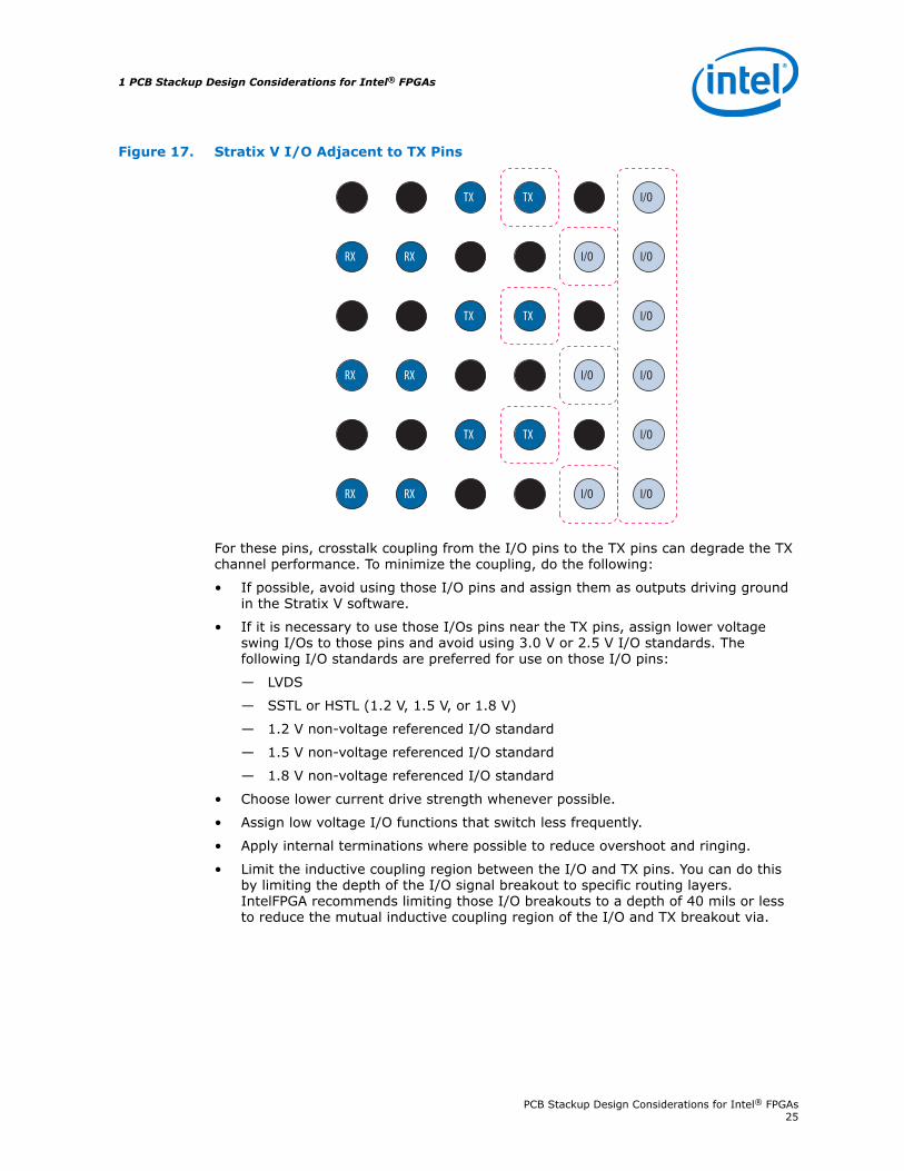
Figure 17. Stratix V I/O Adjacent to TX Pins
TX
TX
TXTX
RXRX
RXRX
RXRX
TX
TX
I/O
I/O
I/O
I/O
I/O
I/OI/O
I/O
I/O
For these pins, crosstalk coupling from the I/O pins to the TX pins can degrade the TXchannel performance. To minimize the coupling, do the following:
• If possible, avoid using those I/O pins and assign them as outputs driving groundin the Stratix V software.
• If it is necessary to use those I/Os pins near the TX pins, assign lower voltageswing I/Os to those pins and avoid using 3.0 V or 2.5 V I/O standards. Thefollowing I/O standards are preferred for use on those I/O pins:
— LVDS
— SSTL or HSTL (1.2 V, 1.5 V, or 1.8 V)
— 1.2 V non-voltage referenced I/O standard
— 1.5 V non-voltage referenced I/O standard
— 1.8 V non-voltage referenced I/O standard
• Choose lower current drive strength whenever possible.
• Assign low voltage I/O functions that switch less frequently.
• Apply internal terminations where possible to reduce overshoot and ringing.
• Limit the inductive coupling region between the I/O and TX pins. You can do thisby limiting the depth of the I/O signal breakout to specific routing layers.IntelFPGA recommends limiting those I/O breakouts to a depth of 40 mils or lessto reduce the mutual inductive coupling region of the I/O and TX breakout via.
1 PCB Stackup Design Considerations for Intel® FPGAs
PCB Stackup Design Considerations for Intel® FPGAs25
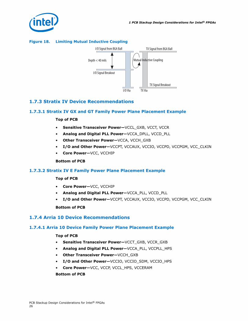
Figure 18. Limiting Mutual Inductive Coupling
I/O Signal from BGA Ball TX Signal from BGA Ball
TX Signal Breakout
Depth < 40 mils
I/O Signal Breakout
I/O Via TX Via
Mutual Inductive Coupling
1.7.3 Stratix IV Device Recommendations
1.7.3.1 Stratix IV GX and GT Family Power Plane Placement Example
Top of PCB
• Sensitive Transceiver Power—VCCL_GXB, VCCT, VCCR
• Analog and Digital PLL Power—VCCA_DPLL, VCCD_PLL
• Other Transceiver Power—VCCA, VCCH_GXB
• I/O and Other Power—VCCPT, VCCAUX, VCCIO, VCCPD, VCCPGM, VCC_CLKIN
• Core Power—VCC, VCCHIP
Bottom of PCB
1.7.3.2 Stratix IV E Family Power Plane Placement Example
Top of PCB
• Core Power—VCC, VCCHIP
• Analog and Digital PLL Power—VCCA_PLL, VCCD_PLL
• I/O and Other Power—VCCPT, VCCAUX, VCCIO, VCCPD, VCCPGM, VCC_CLKIN
Bottom of PCB
1.7.4 Arria 10 Device Recommendations
1.7.4.1 Arria 10 Device Family Power Plane Placement Example
Top of PCB
• Sensitive Transceiver Power—VCCT_GXB, VCCR_GXB
• Analog and Digital PLL Power—VCCA_PLL, VCCPLL_HPS
• Other Transceiver Power—VCCH_GXB
• I/O and Other Power—VCCIO, VCCIO_SDM, VCCIO_HPS
• Core Power—VCC, VCCP, VCCL_HPS, VCCERAM
Bottom of PCB
1 PCB Stackup Design Considerations for Intel® FPGAs
PCB Stackup Design Considerations for Intel® FPGAs26
1.7.5 Arria V Device Recommendations
1.7.5.1 Arria V Device Family Power Plane Placement Example
Top of PCB
• Sensitive Transceiver Power—VCCT_GXB, VCCR_GXB, VCCL_GXB
• Analog and Digital PLL Power—VCCA_FPLL, VCCD_FPLL, VCCPLL_HPS
• Other Transceiver Power—VCCA_GXB, VCCH_GXB
• I/O and Other Power—VCCIO, VCCIO_HPS, VCCPD, VCCPD_HPS
• Core Power—VCC, VCCP, VCC_HPS
Bottom of PCB
1.7.6 Arria II Device Recommendations
1.7.6.1 Arria II GX Family Power Plane Placement Example
Top of PCB
• Sensitive Transceiver Power—VCCL_GXB
• Analog and Digital PLL Power—VCCA_PLL, VCCD_PLL
• Other Transceiver Powerr—VCCA, VCCH_GXB
• I/O and Other Power—VCCIO, VCCPD, VCCCB
• Core Power—VCC
Bottom of PCB
1.7.7 Cyclone 10 Device Recommendations
1.7.7.1 Cyclone 10 LP Device Family Power Plane Placement Example
Top of PCB
• Analog and Digital PLL Power—VCCA, VCCD_PLL
• I/O and Other Power—VCCIO
• Core Power—VCCINT
Bottom of PCB
1.7.8 Cyclone V Device Recommendations
1.7.8.1 Cyclone V Device Family Power Plane Placement Example
Top of PCB
1 PCB Stackup Design Considerations for Intel® FPGAs
PCB Stackup Design Considerations for Intel® FPGAs27
• Sensitive Transceiver Power—VCCE_GXB, VCCL_GXB
• Analog and Digital PLL Power—VCCA_FPLL, VCCPLL_HPS
• Other Transceiver Power—VCCH_GXB
• I/O and Other Power—VCCIO, VCCPD, VCCPGM, VCCIO_HPS, VCCPD_HPS
• Core Power—VCC, VCC_HPS
Bottom of PCB
1.7.9 Cyclone IV Device Recommendations
1.7.9.1 Cyclone IV GX Family Power Plane Placement Example
Top of PCB
• Sensitive Transceiver Power—VCCL_GXB
• Analog and Digital PLL Power—VCCA, VCCD_PLL
• Other Transceiver Power—VCCA_GXB, VCCH_GXB
• I/O and Other Power—VCCIO, VCC_CLKIN
• Core Power—VCCINT
Bottom of PCB
1.7.9.2 Cyclone IV E Family Power Plane Placement Example
Top of PCB
• Core Power— VCCINT
• Analog and Digital PLL Power—VCCA, VCCD_PLL
• I/O and Other Power—VCCIO, VCC_CLKIN
Bottom of PCB
1.7.10 Cyclone III Device Recommendations
1.7.10.1 Cyclone III Family Power Plane Placement Example
Top of PCB
• Core Power—VCCINT
• PLL Power—VCCA, VCCD_PLL
• I/O Power—VCCIO
Bottom of PCB
1.8 References
Base Materials for High Speed, High Frequency PC Boards, Rick Hartley, PCB&A, Mar2002
1 PCB Stackup Design Considerations for Intel® FPGAs
PCB Stackup Design Considerations for Intel® FPGAs28
High-Speed Digital Design, Handbook of Black Magic, Howard Johnson & MartinGraham, Professional Technical Reference, Upper Saddle River, NJ 07458, 1993
Military Standard Printed Wiring for Electronic Equipment (Mil-Std-275E) Specification,Dec 1984
Signal Integrity – Simplified, Dr. Eric Bogatin, Prentice Hall Professional TechnicalReference, Upper Saddle River, NJ 07458, Dec 2006
Survey and Tutorial of Dielectric Materials Used In the Manufacture of Printed Circuit,Lee W. Ritchey, Speeding Edge, Circuitree Magazine, Nov 1999
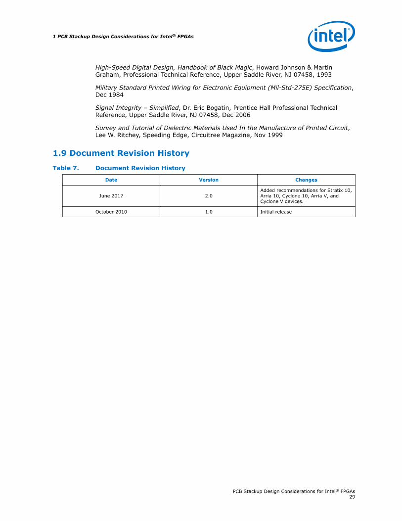
1.9 Document Revision History
Table 7. Document Revision History
Date Version Changes
June 2017 2.0Added recommendations for Stratix 10,Arria 10, Cyclone 10, Arria V, andCyclone V devices.
October 2010 1.0 Initial release
1 PCB Stackup Design Considerations for Intel® FPGAs
PCB Stackup Design Considerations for Intel® FPGAs29