Embed Size (px)
Citation preview
Page 1
TERASPEED
CONSULTING
GROUPAFFILIATE
© 2009, IPBLOX LLC, All Rights Reserved
DesignCon 2009
PCB Power Delivery Optimizations for the
Cost Driven Era
Steve Weir
IPBLOX, LLC
Tom Dagostino
Teraspeed Labs/Z2 Consulting
Page 2
TERASPEED
CONSULTING
GROUPAFFILIATE
© 2009, IPBLOX LLC, All Rights Reserved
Property Rights Disclosure
“PROPERTY OF TERASPEED CONSULTING GROUP LLC
INCLUDES MATERIALS LICENSED FROM IPBLOX LLC”
Information contained in this document is not to be reproduced in any
form without permission of Teraspeed Consulting Group LLC. Any
information in this document is proprietary and may not be used or
disclosed without the express permission of Teraspeed Consulting Group
LLC.
“CONFIDENTIAL PROPERTY OF TERASPEED CONSULTING
GROUP LLC, IPBLOX LLC”
This document includes valuable trade secrets. Unauthorized disclosure
of use of this document may violate the Uniform Trade Secrets Act.
Page 3
TERASPEED
CONSULTING
GROUPAFFILIATE
© 2009, IPBLOX LLC, All Rights Reserved
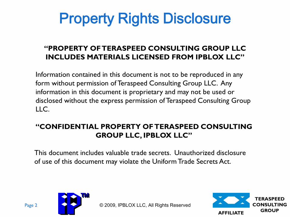
The Power Deliver Problem
• Support DC current requirements of each IC
• Support AC current requirements of each IC
• Sufficiently suppress AC noise between
separate IC power nodes and ICs
• Support I/O return path impedance
requirements
• Meet emissions and susceptibility
requirements

Page 4
TERASPEED
CONSULTING
GROUPAFFILIATE
© 2009, IPBLOX LLC, All Rights Reserved
Divide and Conquer
• Divide the problem between what is on the
PCB and the requirements and parasitics of
each IC
• Results in impedance budget for each IC at
the PCB attach

Page 5
TERASPEED
CONSULTING
GROUPAFFILIATE
© 2009, IPBLOX LLC, All Rights Reserved
What We Can Control On the PCB
• PCB stack-up
• PCB laminate selection
• Bypass capacitor selection
• Bypass network design
• Choices interact

Page 6
TERASPEED
CONSULTING
GROUPAFFILIATE
© 2009, IPBLOX LLC, All Rights Reserved
Power Plane Behavior
• Power plane cavities exhibit two distinct behaviors:
– Distributed impedance• How the cavity appears to many loads distributed over
the cavity X-Y extents
• Very low inductance, modest value capacitor
• Thin cavities increase capacitance
– Local impedance• How the cavity appears to any given load
• Series R-L out to bypass caps & VRM
• Thin cavities decrease inductance
Page 7
TERASPEED
CONSULTING
GROUPAFFILIATE
© 2009, IPBLOX LLC, All Rights Reserved
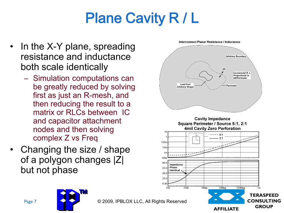
Plane Cavity R / L
• In the X-Y plane, spreading resistance and inductance both scale identically – Simulation computations can
be greatly reduced by solving first as just an R-mesh, and then reducing the result to a matrix or RLCs between IC and capacitor attachment nodes and then solving complex Z vs Freq
• Changing the size / shape of a polygon changes |Z| but not phase

Page 8
TERASPEED
CONSULTING
GROUPAFFILIATE
© 2009, IPBLOX LLC, All Rights Reserved
Cavity Height and Complex Z
• R/L behavior depends on:– Conductor bulk
resistance,
– Skin effect,
– Conductor relative permeability, 1.0 for copper
– Cavity dielectric height
• Reflected as phase response of interconnect alone
Page 9
TERASPEED
CONSULTING
GROUPAFFILIATE
© 2009, IPBLOX LLC, All Rights Reserved
Cavity Height and Complex Z
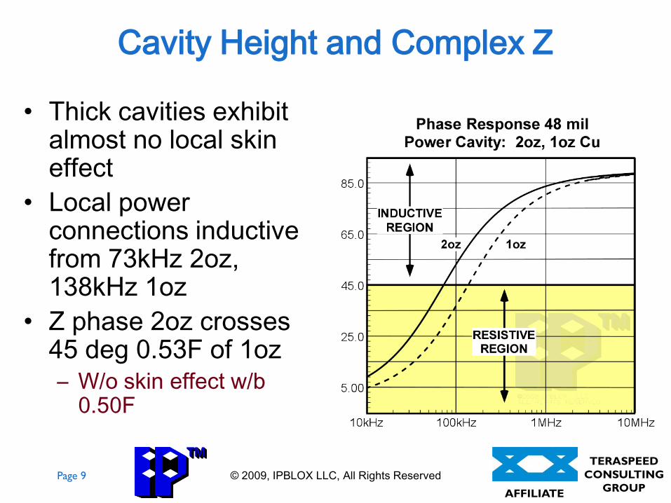
• Thick cavities exhibit almost no local skin effect
• Local power connections inductive from 73kHz 2oz, 138kHz 1oz
• Z phase 2oz crosses 45 deg 0.53F of 1oz– W/o skin effect w/b
0.50F
Page 10
TERASPEED
CONSULTING
GROUPAFFILIATE
© 2009, IPBLOX LLC, All Rights Reserved
Cavity Height and Complex Z
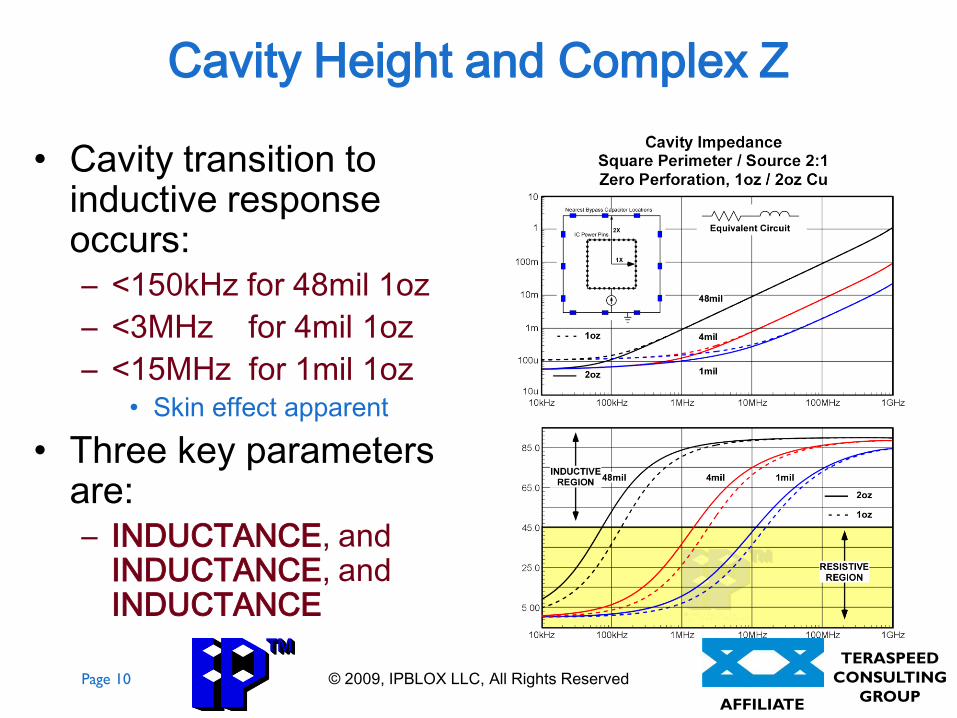
• Cavity transition to inductive response occurs:– <150kHz for 48mil 1oz
– <3MHz for 4mil 1oz
– <15MHz for 1mil 1oz• Skin effect apparent
• Three key parameters are: – INDUCTANCE, and
INDUCTANCE, and INDUCTANCE
Page 11
TERASPEED
CONSULTING
GROUPAFFILIATE
© 2009, IPBLOX LLC, All Rights Reserved
PDN as Collection of Local PDNs
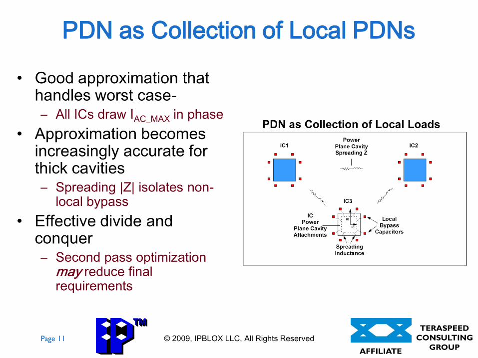
• Good approximation that handles worst case-– All ICs draw IAC_MAX in phase
• Approximation becomes increasingly accurate for thick cavities– Spreading |Z| isolates non-
local bypass
• Effective divide and conquer – Second pass optimization
may reduce final requirements

Page 12
TERASPEED
CONSULTING
GROUPAFFILIATE
© 2009, IPBLOX LLC, All Rights Reserved
PDN as Collection of Local PDNs
• Solve PDN for each IC
first
• Adjust for full
optimization second
– Useful tools: Optimize
PI™, Hyperlinx™, SI-
Wave™
• Adjust for resonances
and EMI hot-spots third

Page 13
TERASPEED
CONSULTING
GROUPAFFILIATE
© 2009, IPBLOX LLC, All Rights Reserved
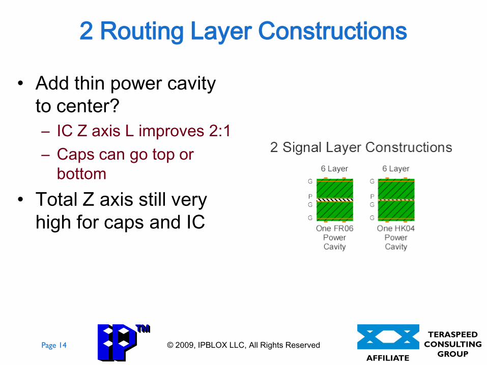
2 Routing Layer Constructions
• 4 layer, thick power cavity traditional– Very high impedance
cavity• Typical 300pH LSPREAD to
IC power
– Peripheral bypass caps below 300pH little effect
– < 300pH Relies on enough power / gnd pairs directly under IC to bottom of PCB and caps to match
Page 14
TERASPEED
CONSULTING
GROUPAFFILIATE
© 2009, IPBLOX LLC, All Rights Reserved
2 Routing Layer Constructions
• Add thin power cavity
to center?
– IC Z axis L improves 2:1
– Caps can go top or
bottom
• Total Z axis still very
high for caps and IC

Page 15
TERASPEED
CONSULTING
GROUPAFFILIATE
© 2009, IPBLOX LLC, All Rights Reserved
2 Routing Layer Constructions
• Add thin power cavities
to outside
– IC Z axis very low
– Cap attach very low
– L/R spreading very low
• Bottom cavity natural
puddle, or add’l route (
4mil ), or combination

Page 16
TERASPEED
CONSULTING
GROUPAFFILIATE
© 2009, IPBLOX LLC, All Rights Reserved
4 Routing Layer Constructions
• Traditional 6 layer
same as 4 layer
– For Tx line return
purposes 2 PCBs, top
and bottom
• 8 layer constructions
very different than 6
layer
– IC Z axis drops
– 2 power cavities
• Can puddle bottom

Page 17
TERASPEED
CONSULTING
GROUPAFFILIATE
© 2009, IPBLOX LLC, All Rights Reserved
Caps Req’d Versus L
• Caps peripheral to IC
using thick cavities:
– Poor effectiveness
• Caps under IC
– Works adequately if IC
mfg provides enough
pwr/gnd via pairs
– If not 4 layer design
won’t work

Page 18
TERASPEED
CONSULTING
GROUPAFFILIATE
© 2009, IPBLOX LLC, All Rights Reserved
Caps Req’d Versus L
• Caps peripheral to IC
using thin cavities:
– Can eliminate many
caps
– How many depends on
target L, cavity thickness
– Only works down to LSAT 0402 X2Y LSAT
4 layer, 50 mil center 6 2 625pH
6 layer, 4 mil center 41 11 50pH
6 layer, 4 mil top 21 6 50pH
6 layer, 1 mil top 81 24 13pH Figure 1, Inductance Saturation Capacitor Counts , Typical
Page 19
TERASPEED
CONSULTING
GROUPAFFILIATE
© 2009, IPBLOX LLC, All Rights Reserved
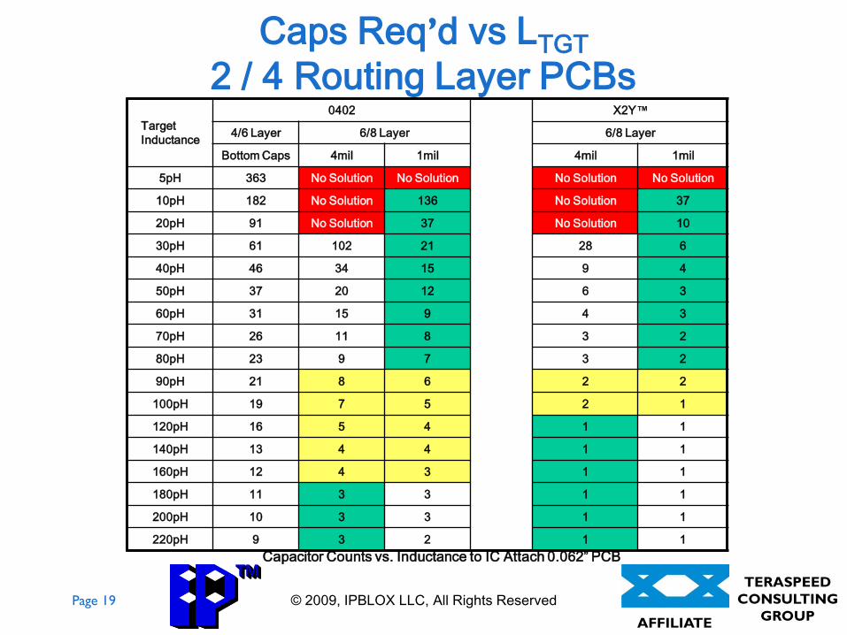
Caps Req’d vs LTGT
2 / 4 Routing Layer PCBsTarget
Inductance
0402 X2Y™
4/6 Layer 6/8 Layer 6/8 Layer
Bottom Caps 4mil 1mil 4mil 1mil
5pH 363 No Solution No Solution No Solution No Solution
10pH 182 No Solution 136 No Solution 37
20pH 91 No Solution 37 No Solution 10
30pH 61 102 21 28 6
40pH 46 34 15 9 4
50pH 37 20 12 6 3
60pH 31 15 9 4 3
70pH 26 11 8 3 2
80pH 23 9 7 3 2
90pH 21 8 6 2 2
100pH 19 7 5 2 1
120pH 16 5 4 1 1
140pH 13 4 4 1 1
160pH 12 4 3 1 1
180pH 11 3 3 1 1
200pH 10 3 3 1 1
220pH 9 3 2 1 1
Capacitor Counts vs. Inductance to IC Attach 0.062” PCB

Page 20
TERASPEED
CONSULTING
GROUPAFFILIATE
© 2009, IPBLOX LLC, All Rights Reserved
Caps Req’d vs LTGT
2 / 4 Routing Layer PCBs
• At modest LTGT:– 90pH < LTGT < 300pH
4mil, 1mil drops caps ≈ 3:1, 4:1 versus 50/42mil
• More demanding LTGT more advantage to 1mil versus 4mil cavities
• Combination of 1mil and X2Y® 10:1 cap reduction from 200pH down to 20pH LTGT
– 200pH 63mOhms @ 50MHz
– 20pH 6.3mOhms @ 50MHz
Target
Inductan
ce
0402 X2Y™
4/6
Layer6/8 Layer 6/8 Layer
Bottom
Caps4mil 1mil 4mil 1mil
5pH 363No
Solution
No
SolutionNo Solution
No
Solution
10pH 182No
Solution136 No Solution 37
20pH 91No
Solution37 No Solution 10
30pH 61 102 21 28 6
40pH 46 34 15 9 4
50pH 37 20 12 6 3
60pH 31 15 9 4 3
70pH 26 11 8 3 2
80pH 23 9 7 3 2
90pH 21 8 6 2 2
100pH 19 7 5 2 1
120pH 16 5 4 1 1
140pH 13 4 4 1 1
160pH 12 4 3 1 1
180pH 11 3 3 1 1
200pH 10 3 3 1 1
220pH 9 3 2 1 1
Page 21
TERASPEED
CONSULTING
GROUPAFFILIATE
© 2009, IPBLOX LLC, All Rights Reserved
Evaluating Costs
• Evaluation comes down to the big three:
– PCB material cost
– Bypass caps, BOM cost
– Bypass caps, placement cost
• Conventional bypass caps are almost free
– $0.001 typical in high volume
• Assembly placement cost is the critical
parameter for both more and/or better PCB
materials and/or better caps

Page 22
TERASPEED
CONSULTING
GROUPAFFILIATE
© 2009, IPBLOX LLC, All Rights Reserved
Evaluating Costs
• At current prices, break-even on 4/6 layer alternatives occurs near $0.01 / comp placement– Why?
• Adding 1 layer of FR406 adds $2.00/sq ft / $0.014 / sq”
– Save 1.3 caps / sq” pays back - $2.00 / ( 144 * $0.011 )
• Changing 2 layers of FR406 to HK04 adds $6.00/sq ft
– Save 3.8 caps / sq” pays back - $6.00 / ( 144 * $0.011 )
• X2Y™ replaces caps ≈ 4:1
– $0.03 comp + $0.01 place ≈ $0.004 comp + $0.04 place
• Key drivers: – Performance targets and
– Assembly cost

Page 23
TERASPEED
CONSULTING
GROUPAFFILIATE
© 2009, IPBLOX LLC, All Rights Reserved
Example Cases
• 4” x 8” PCB
• Ten IC’s 70pH LTGT
– 22mOhms @ 50MHz
• 2 routing layers
• $2.00/sq ft FR406 / layer pair
• $5.00/sq ft HK04™ / layer pair
• $0.001 / cap 0402
• $0.03 / cap X2Y™
• $0.015 / cap assy

Page 24
TERASPEED
CONSULTING
GROUPAFFILIATE
© 2009, IPBLOX LLC, All Rights Reserved
Example Cases
• 4” x 8” PCB
• 4 routing layers
• 12 ICs 50pH LTGT
– 15mOhms @ 50MHz
• $2.00/sq ft FR406 / layer pair
• $5.00/sq ft HK04™ / layer pair
• $0.001 / cap 0402
• $0.03 / cap X2Y™
• $0.015 / cap assy

Page 25
TERASPEED
CONSULTING
GROUPAFFILIATE
© 2009, IPBLOX LLC, All Rights Reserved
Conclusions
• Power distribution focus is managing inductance
• PCBs are locally inductive from low frequencies– Transition frequency independent of plane shape
– Inductance proportional to thickness
• Thinner dielectric allows more inductance in bypass cap network, IE fewer caps
• In many low-cost constructions, total manufactured cost can be minimized through use of:– More material – take 4 to 6 layer, or 6 to 8 layer w/ glass / resin cavities
– More expensive raw materials – using 1 mil polyimide ( DuPont Interra HK04® ), or epoxy ( Oak/Mitsui BC24® ) dielectric in place of 4 mil glass / resin
– Lower inductance capacitors such as X2Y™
• Thinner cavities offer other performance benefits, but here we are concerned only with cost and presume function can be realized w/thick cavities
• Actual results depend on IC LTGT and assembly cost per capacitor– Know your requirements!
– Know your costs!
Page 26
TERASPEED
CONSULTING
GROUPAFFILIATE
© 2009, IPBLOX LLC, All Rights Reserved
How To Contact Us?IPBLOX, LLC
150 N. Center St. #211
Reno, NV 89501
v (866) 675-4630
f (707) 780-1951
www.ipblox.com
Power Delivery Solutions
Teraspeed Consulting Group, LLC
121 North River Drive
Narragansett, RI 02882
v (401) 284-1827
f (401) 284-1840
www.teraspeed.com
3D E/M Modeling
Z2 Consulting
13610 SW Harness Lane
Portland, OR 93007
v (503) 430-1065
f (401) 284-1840
www.teraspeed.com
Metrology
Measurement based IBIS models
Sage Consulting
13610 SW Harness Lane
Portland, OR 93007
v (503) 679-2429
f (401) 284-1840
www.teraspeed.com
Serial link development
Jitter analysis
Teraspeed Consulting Group, LLC
Other Affiliates