Embed Size (px)
Citation preview
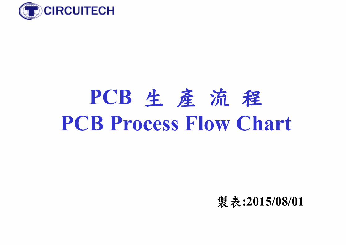
PCB 生 產 流 程PCB Process Flow Chart
製表:2015/08/01
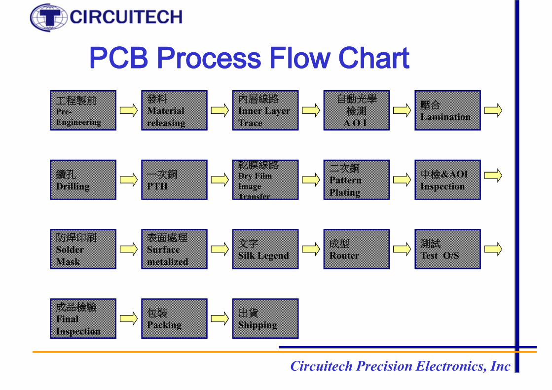
PCB Process Flow ChartPCB Process Flow Chart
成品檢驗Final Inspection
出貨Shipping
包裝Packing
文字Silk Legend
表面處理Surface metalized
測試Test O/S
成型Router
防焊印刷Solder Mask
鑽孔Drilling
乾膜線路Dry Film Image Transfer
一次銅PTH
中檢&AOIInspection
二次銅PatternPlating
發料Material releasing
內層線路Inner Layer Trace
自動光學檢測
A O I
壓合Lamination
工程製前Pre-Engineering
Circuitech Precision Electronics, Inc.
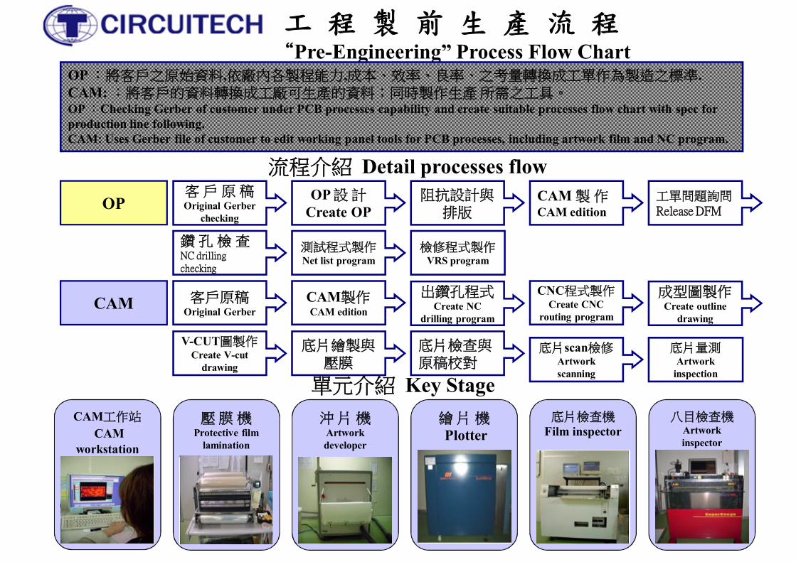
工 程 製 前 生 產 流 程“Pre-Engineering” Process Flow Chart
OP :將客戶之原始資料,依廠內各製程能力,成本、效率、良率、之考量轉換成工單作為製造之標準.CAM: :將客戶的資料轉換成工廠可生產的資料;同時製作生產 所需之工具。OP :Checking Gerber of customer under PCB processes capability and create suitable processes flow chart with spec for production line following.CAM: Uses Gerber file of customer to edit working panel tools for PCB processes, including artwork film and NC program.
流程介紹 Detail processes flow
OP
CAM
單元介紹 Key Stage
客 戶 原 稿Original Gerber
checking
OP 設 計Create OP
阻抗設計與排版
CAM 製 作CAM edition
鑽 孔 檢 查NC drillingchecking
測試程式製作Net list program
檢修程式製作VRS program
V-CUT圖製作Create V-cut
drawing
底片繪製與壓膜
底片量測Artwork
inspection
客戶原稿Original Gerber
CAM製作CAM edition
底片檢查與原稿校對
工單問題詢問Release DFM
出鑽孔程式Create NC
drilling program
底片scan檢修Artwork scanning
CNC程式製作Create CNC
routing program
成型圖製作Create outline
drawing
CAM工作站
CAM workstation
壓 膜 機Protective film
lamination
沖 片 機Artwork developer
繪 片 機Plotter
底片檢查機Film inspector
八目檢查機Artwork inspector
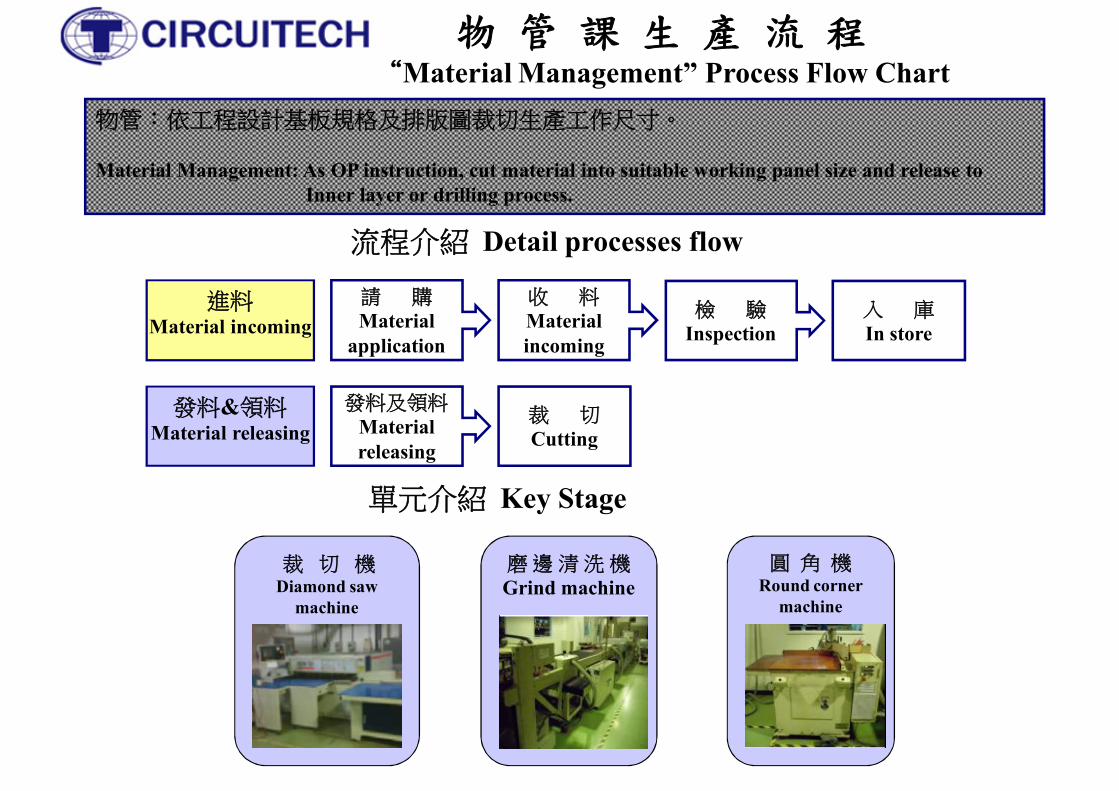
物 管 課 生 產 流 程“Material Management” Process Flow Chart
物管:依工程設計基板規格及排版圖裁切生產工作尺寸。
Material Management: As OP instruction, cut material into suitable working panel size and release toInner layer or drilling process.
流程介紹 Detail processes flow
進料Material incoming
發料&領料Material releasing
單元介紹 Key Stage
請 購Material
application
收 料Material incoming
檢 驗Inspection
發料及領料Material releasing
裁 切Cutting
入 庫In store
裁 切 機Diamond saw
machine
磨 邊 清 洗 機Grind machine
圓 角 機Round corner
machine
內 層 課 生 產 流 程“Inner Layer” Process Flow Chart
內層:在基板表面塗布感光油墨,利用影像轉移的方式將線路圖形轉移到基板表面油墨上,再通過顯影、蝕刻和去膜的製成製作內層板。
Inner Layer:Coating the film of photosensitive ink by roller on the CCL surface, transfer the pattern onCCL with UV light through artwork film, like photo; then have the development, etching and striping stage to finish whole process.
流程介紹 Detail processes flow油墨塗布
Film coating
曝光/蝕刻Exposure/Etching
AOI
單元介紹 Key Stage
前 處 理Pre-treatment
油 墨 塗 布Coating ink
烘 烤Curing
內層前處理Pre-treatment
水平塗布Roller Coating
曝 光Exposure
自動光學檢測 AOI
CCD鑽孔Drill Tooling Holes
內層蝕刻Etching
CCD 鑽 孔Drill tooling
holes
自動光學檢測
AOI檢 修
VRS
曝 光Exposure
顯 影Developing
蝕 刻Acid etching
去 膜Striping
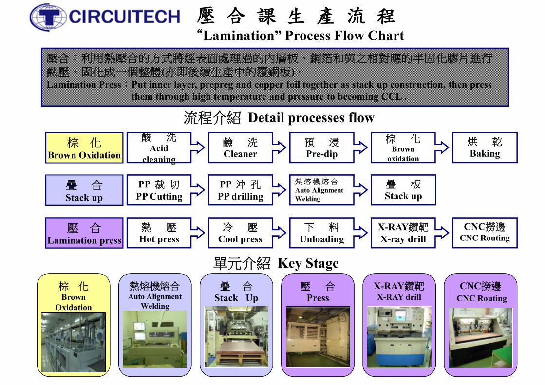
壓 合 課 生 產 流 程“Lamination” Process Flow Chart
壓合:利用熱壓合的方式將經表面處理過的內層板、銅箔和與之相對應的半固化膠片進行熱壓、固化成一個整體(亦即後續生產中的覆銅板)。Lamination Press:Put inner layer, prepreg and copper foil together as stack up construction, then press
them through high temperature and pressure to becoming CCL .
流程介紹 Detail processes flow
棕 化Brown Oxidation
疊 合Stack up
壓 合Lamination press
單元介紹 Key Stage
酸 洗Acid
cleaning
鹼 洗Cleaner
預 浸Pre-dip
棕 化Brown
oxidation
烘 乾Baking
PP 裁 切PP Cutting
PP 沖 孔PP drilling
疊 板Stack up
熱 熔 機 熔 合Auto Alignment Welding
熱 壓Hot press
冷 壓Cool press
下 料Unloading
X-RAY鑽靶X-ray drill
CNC撈邊CNC Routing
棕 化Brown
Oxidation
熱熔機熔合Auto Alignment
Welding
疊 合Stack Up
壓 合Press
X-RAY鑽靶X-RAY drill
CNC撈邊CNC Routing
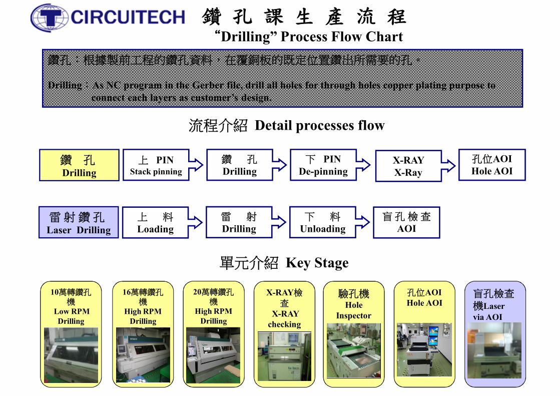
鑽 孔 課 生 產 流 程“Drilling” Process Flow Chart
鑽孔:根據製前工程的鑽孔資料,在覆銅板的既定位置鑽出所需要的孔。
Drilling:As NC program in the Gerber file, drill all holes for through holes copper plating purpose toconnect each layers as customer’s design.
流程介紹 Detail processes flow
鑽 孔Drilling
雷 射 鑽 孔Laser Drilling
單元介紹 Key Stage
上 PINStack pinning
鑽 孔Drilling
孔位AOI Hole AOI
下 PINDe-pinning
雷 射Drilling
下 料Unloading
上 料Loading
盲 孔 檢 查AOI
10萬轉鑽孔機
Low RPM Drilling
16萬轉鑽孔機
High RPM Drilling
X-RAY檢查
X-RAY checking
驗孔機Hole
Inspector
盲孔檢查機Laser via AOI
20萬轉鑽孔機
High RPM Drilling
X-RAY X-Ray
孔位AOIHole AOI
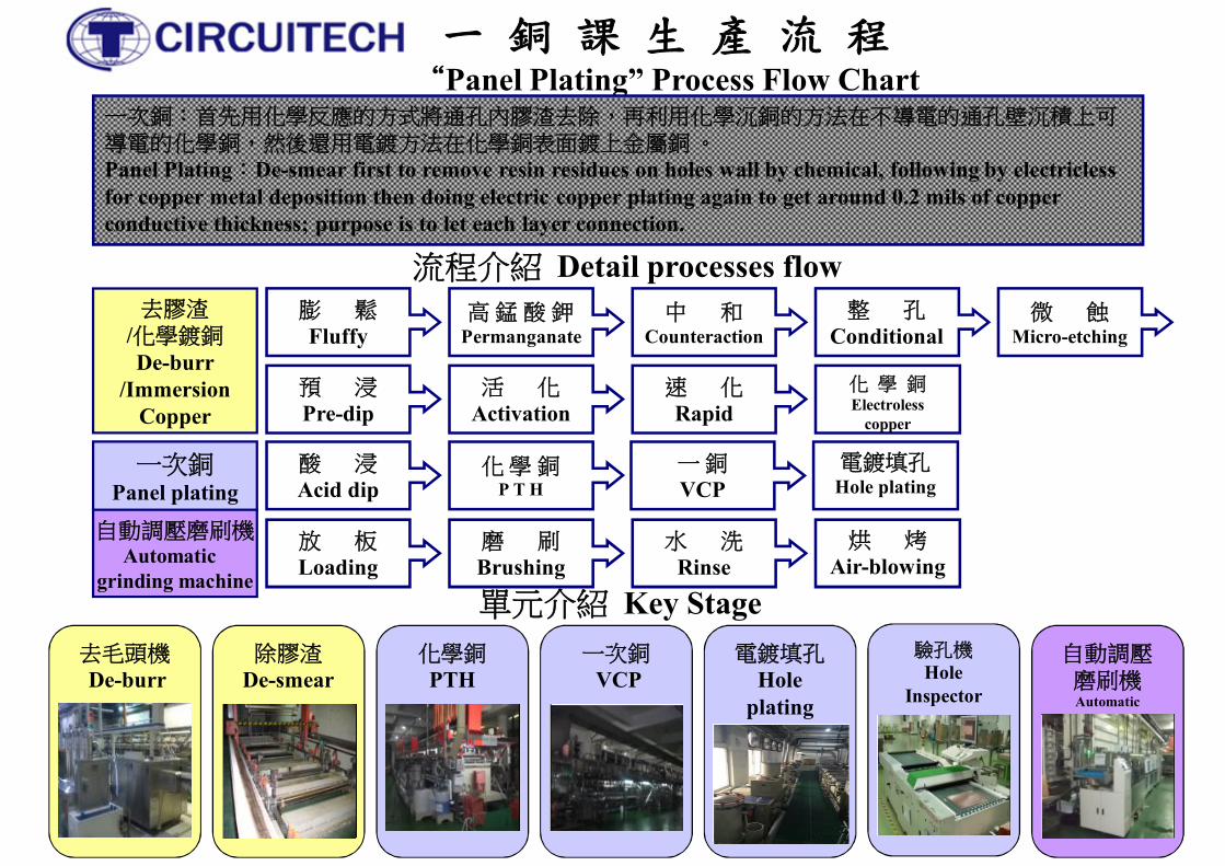
一 銅 課 生 產 流 程“Panel Plating” Process Flow Chart
一次銅:首先用化學反應的方式將通孔內膠渣去除,再利用化學沉銅的方法在不導電的通孔壁沉積上可導電的化學銅,然後還用電鍍方法在化學銅表面鍍上金屬銅 。Panel Plating:De-smear first to remove resin residues on holes wall by chemical, following by electricless for copper metal deposition then doing electric copper plating again to get around 0.2 mils of copper conductive thickness; purpose is to let each layer connection.
流程介紹 Detail processes flow去膠渣
/化學鍍銅De-burr
/Immersion Copper
一次銅Panel plating
自動調壓磨刷機Automatic
grinding machine單元介紹 Key Stage
膨 鬆Fluffy
高 錳 酸 鉀Permanganate
中 和Counteraction
整 孔Conditional
預 浸Pre-dip
活 化Activation
化 學 銅Electroless
copper
放 板Loading
磨 刷Brushing
烘 烤Air-blowing
酸 浸Acid dip
化 學 銅P T H
水 洗Rinse
電鍍填孔Hole plating
微 蝕Micro-etching
速 化Rapid
除膠渣De-smear
化學銅PTH
一次銅VCP
電鍍填孔Hole
plating
自動調壓磨刷機Automatic grinding
去毛頭機De-burr
一 銅VCP
驗孔機Hole
Inspector
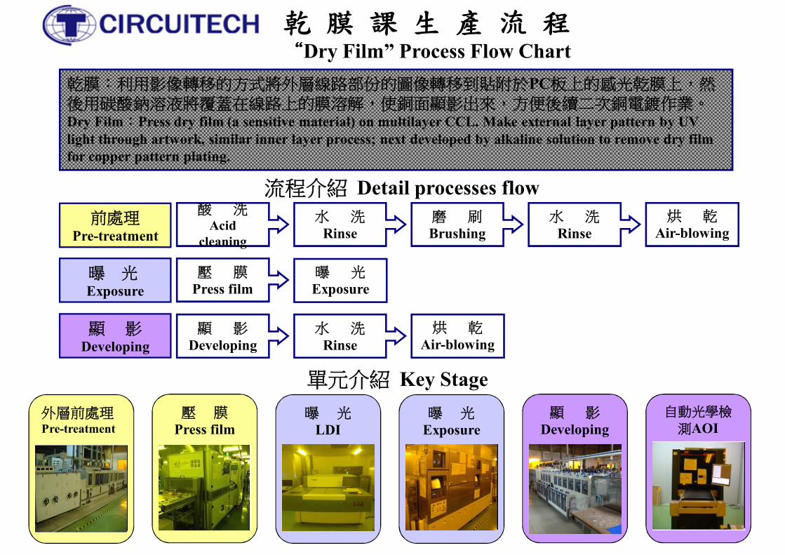
乾 膜 課 生 產 流 程“Dry Film” Process Flow Chart
乾膜:利用影像轉移的方式將外層線路部份的圖像轉移到貼附於PC板上的感光乾膜上,然後用碳酸鈉溶液將覆蓋在線路上的膜溶解,使銅面顯影出來,方便後續二次銅電鍍作業。Dry Film:Press dry film (a sensitive material) on multilayer CCL. Make external layer pattern by UV light through artwork, similar inner layer process; next developed by alkaline solution to remove dry film for copper pattern plating.
流程介紹 Detail processes flow前處理
Pre-treatment
曝 光Exposure
單元介紹 Key Stage
酸 洗Acid
cleaning
水 洗Rinse
磨 刷Brushing
水 洗Rinse
曝 光Exposure
壓 膜Press film
水 洗Rinse
顯 影Developing
烘 乾Air-blowing
顯 影Developing
烘 乾Air-blowing
外層前處理Pre-treatment
曝 光Exposure
自動光學檢
測AOI壓 膜
Press film顯 影
Developing曝 光
LDI
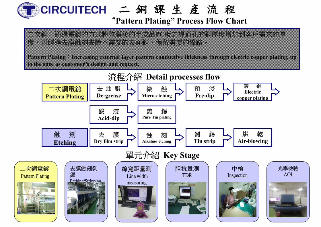
二 銅 課 生 產 流 程“Pattern Plating” Process Flow Chart
二次銅:通過電鍍的方式將乾膜後的半成品PC板之導通孔的銅厚度增加到客戶需求的厚度,再經過去膜蝕刻去除不需要的表面銅,保留需要的線路。
Pattern Plating:Increasing external layer pattern conductive thickness through electric copper plating, up to the spec as customer’s design and request.
流程介紹 Detail processes flow二次銅電鍍
Pattern Plating
蝕 刻Etching
單元介紹 Key Stage
去 油 脂De-grease
微 蝕Micro-etching
預 浸Pre-dip
鍍 銅Electric
copper plating
鍍 錫Pure Tin plating
酸 浸Acid-dip
蝕 刻Alkaline etching
去 膜Dry film strip
烘 乾Air-blowing
剝 錫Tin strip
二次銅電鍍Pattern Plating
線寬距量測Line width measuring
阻抗量測TDR
中檢Inspection
去膜蝕刻剝錫Etching/Stripping
光學檢驗AOI
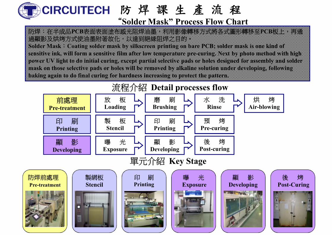
防 焊 課 生 產 流 程“Solder Mask” Process Flow Chart
防焊:在半成品PCB表面表面塗布感光阻焊油墨,利用影像轉移方式將各式圖形轉移至PCB板上,再通過顯影及烘烤方式使油墨附著故化,以達到絕緣阻焊之目的。Solder Mask:Coating solder mask by silkscreen printing on bare PCB; solder mask is one kind of sensitive ink, will form a sensitive film after low temperature pre-curing. Next by photo method with high power UV light to do initial curing, except partial selective pads or holes designed for assembly and solder mask on those selective pads or holes will be removed by alkaline solution under developing, following baking again to do final curing for hardness increasing to protect the pattern.
流程介紹 Detail processes flow前處理
Pre-treatment
印 刷Printing
單元介紹 Key Stage
放 板Loading
磨 刷Brushing
水 洗Rinse
印 刷Printing
預 烤Pre-curing
製 板Stencil
曝 光Exposure
顯 影Developing
後 烤Post-curing
顯 影Developing
烘 烤Air-blowing
防焊前處理Pre-treatment
印 刷Printing
後 烤Post-Curing
顯 影Developing
製網板Stencil
曝 光Exposure
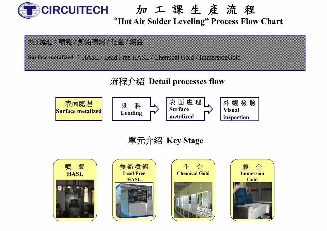
加 工 課 生 產 流 程“Hot Air Solder Leveling” Process Flow Chart
表面處理:噴錫 / 無鉛噴錫 / 化金 / 鍍金
Surface metalized :HASL / Lead Free HASL / Chemical Gold / ImmersionGold
流程介紹 Detail processes flow
表面處理Surface metalized
單元介紹 Key Stage
進 料Loading
表 面 處 理Surface metalized
外 觀 檢 驗Visual inspection
噴 錫HASL
無 鉛 噴 錫Lead Free
HASL
鍍 金Immersion
Gold
化 金Chemical Gold
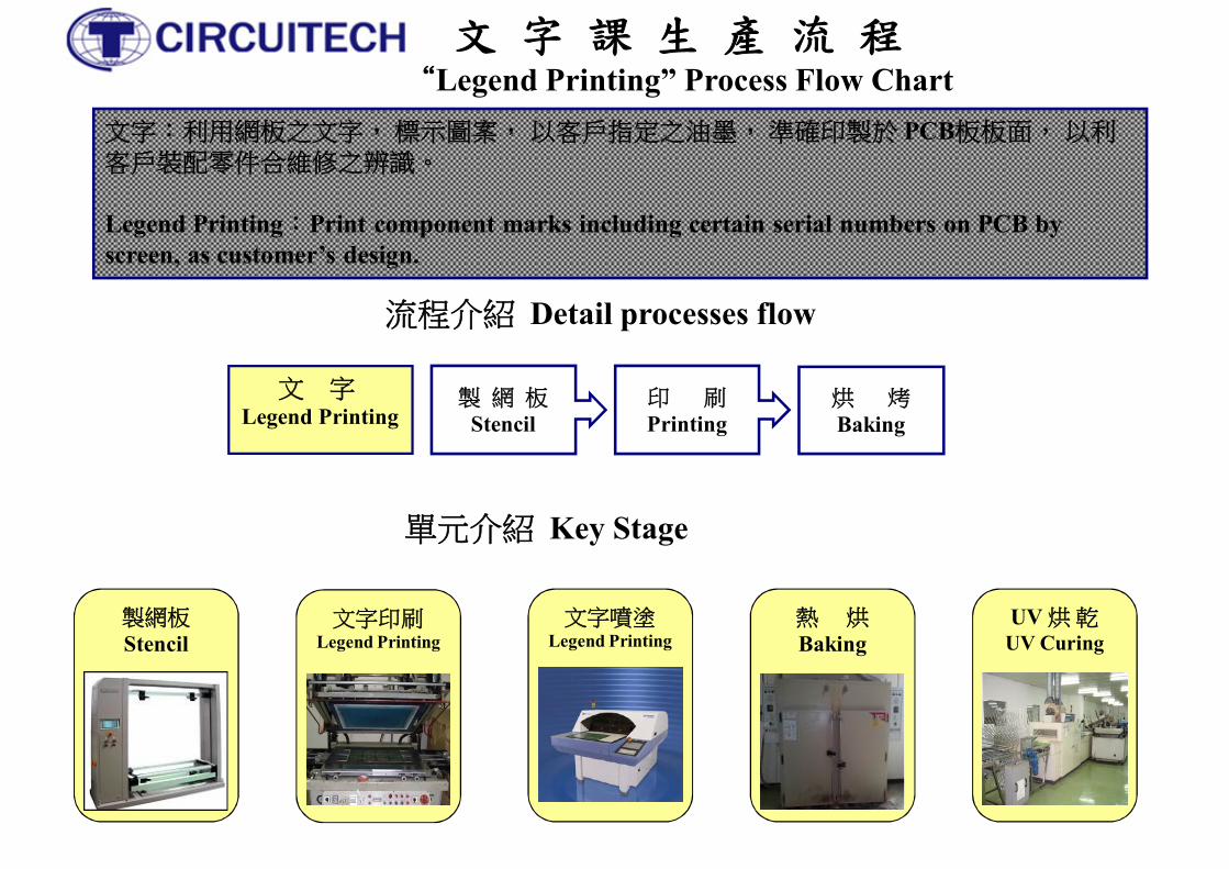
文 字 課 生 產 流 程“Legend Printing” Process Flow Chart
文字:利用網板之文字, 標示圖案, 以客戶指定之油墨, 準確印製於 PCB板板面, 以利客戶裝配零件合維修之辨識。
Legend Printing:Print component marks including certain serial numbers on PCB by screen, as customer’s design.
流程介紹 Detail processes flow
文 字Legend Printing
單元介紹 Key Stage
製 網 板Stencil
印 刷Printing
烘 烤Baking
文字印刷Legend Printing
UV 烘 乾UV Curing
製網板Stencil
熱 烘Baking
文字噴塗Legend Printing
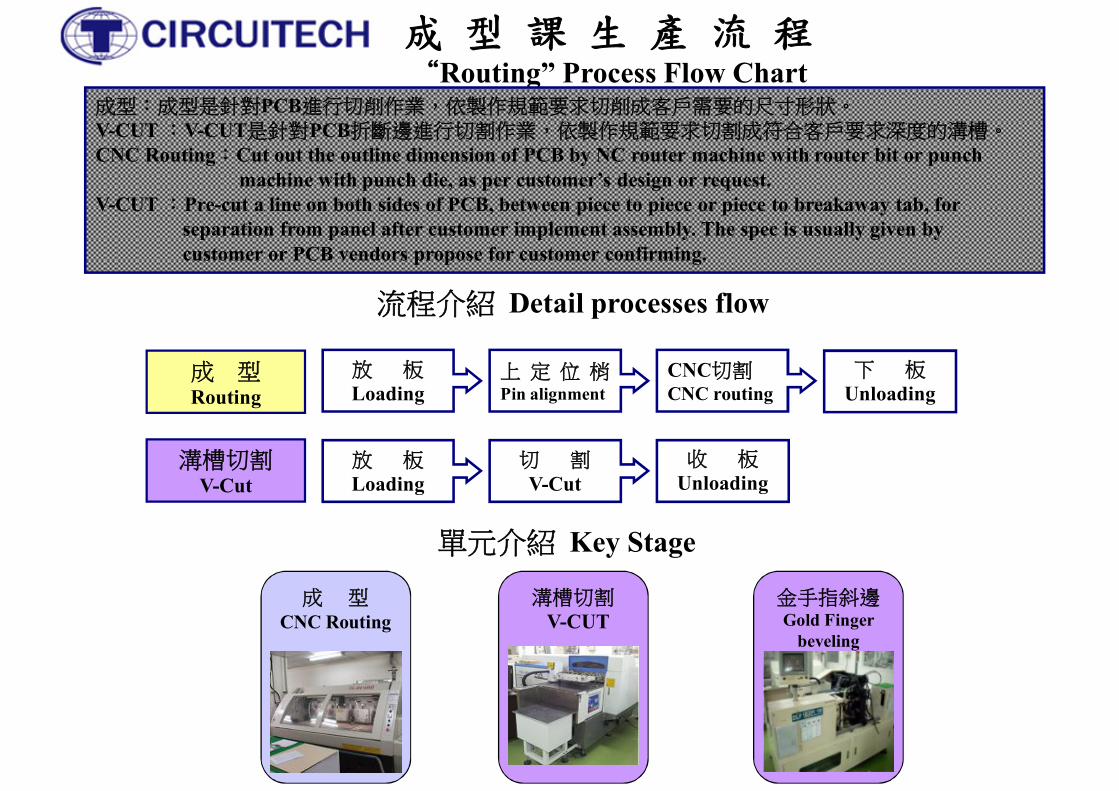
成 型 課 生 產 流 程“Routing” Process Flow Chart
成型:成型是針對PCB進行切削作業,依製作規範要求切削成客戶需要的尺寸形狀。V-CUT :V-CUT是針對PCB折斷邊進行切割作業,依製作規範要求切割成符合客戶要求深度的溝槽。CNC Routing:Cut out the outline dimension of PCB by NC router machine with router bit or punch
machine with punch die, as per customer’s design or request.V-CUT :Pre-cut a line on both sides of PCB, between piece to piece or piece to breakaway tab, for
separation from panel after customer implement assembly. The spec is usually given by customer or PCB vendors propose for customer confirming.
流程介紹 Detail processes flow
成 型Routing
單元介紹 Key Stage
放 板Loading
上 定 位 梢Pin alignment
CNC切割CNC routing
放 板Loading
切 割V-Cut
收 板Unloading
溝槽切割V-Cut
下 板Unloading
金手指斜邊Gold Finger
beveling
成 型CNC Routing
溝槽切割V-CUT
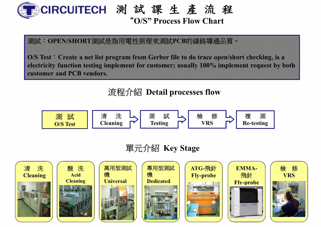
測 試 課 生 產 流 程“O/S” Process Flow Chart
測試:OPEN/SHORT測試是指用電性原理來測試PCB的線路導通品質。
O/S Test:Create a net list program from Gerber file to do trace open/short checking, is a electricity function testing implement for customer; usually 100% implement request by both customer and PCB vendors.
流程介紹 Detail processes flow
測 試O/S Test
單元介紹 Key Stage
清 洗Cleaning
測 試Testing
檢 修VRS
複 測Re-testing
清 洗Cleaning
萬用型測試機Universal Tester
專用型測試機Dedicated Tester
ATG-飛針Fly-probe
檢 修VRS
酸 洗Acid
Cleaning
EMMA-飛針
Fly-probe
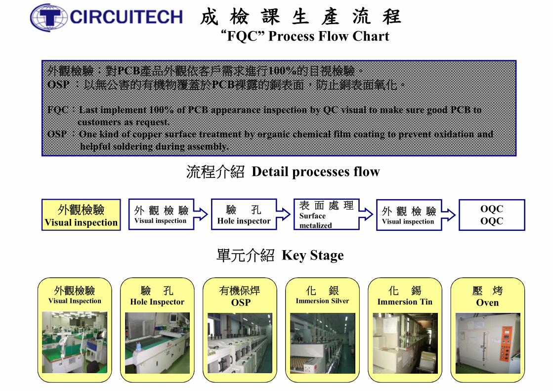
成 檢 課 生 產 流 程“FQC” Process Flow Chart
外觀檢驗:對PCB產品外觀依客戶需求進行100%的目視檢驗。OSP :以無公害的有機物覆蓋於PCB裸露的銅表面,防止銅表面氧化。
FQC:Last implement 100% of PCB appearance inspection by QC visual to make sure good PCB tocustomers as request.
OSP :One kind of copper surface treatment by organic chemical film coating to prevent oxidation andhelpful soldering during assembly.
流程介紹 Detail processes flow
外觀檢驗Visual inspection
單元介紹 Key Stage
外 觀 檢 驗Visual inspection
驗 孔Hole inspector
表 面 處 理Surface metalized
OQCOQC
外 觀 檢 驗Visual inspection
外觀檢驗Visual Inspection
驗 孔Hole Inspector
有機保焊OSP
化 銀Immersion Silver
化 錫Immersion Tin
壓 烤Oven
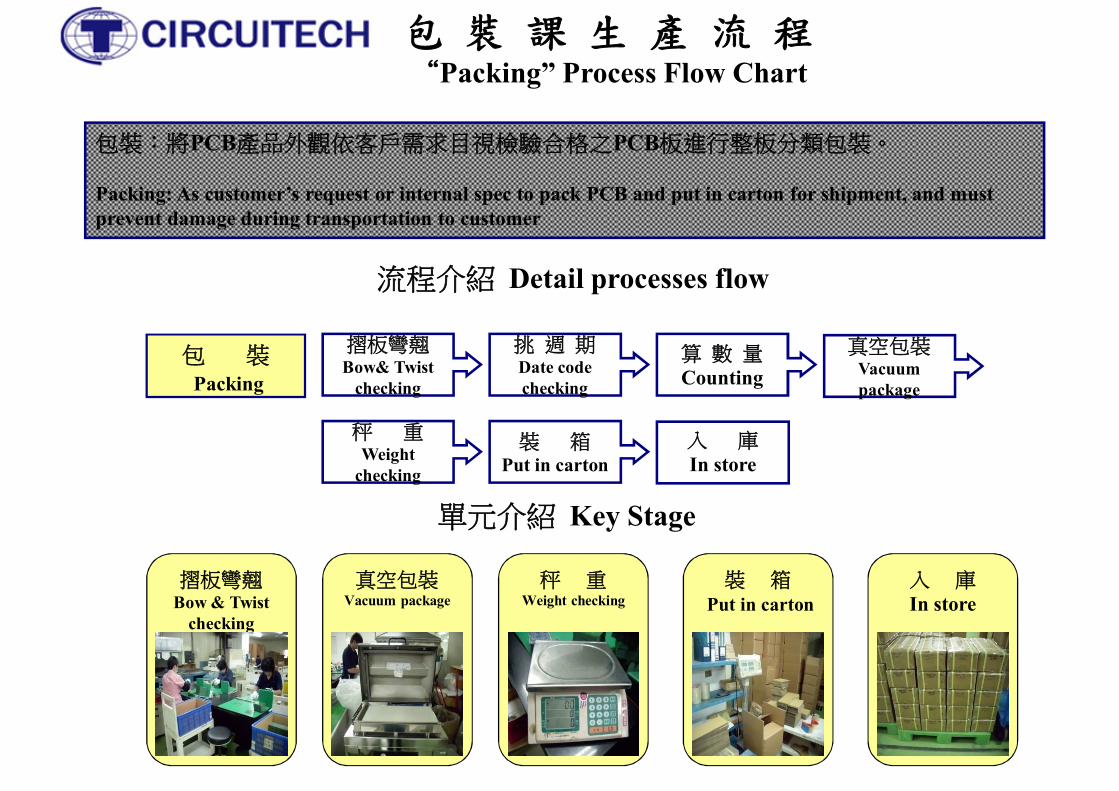
包 裝 課 生 產 流 程“Packing” Process Flow Chart
包裝:將PCB產品外觀依客戶需求目視檢驗合格之PCB板進行整板分類包裝。
Packing: As customer’s request or internal spec to pack PCB and put in carton for shipment, and must prevent damage during transportation to customer
流程介紹 Detail processes flow
包 裝Packing
單元介紹 Key Stage
摺板彎翹Bow& Twist
checking
挑 週 期Date code checking
算 數 量Counting
真空包裝Vacuum package
秤 重Weight
checking
裝 箱Put in carton
入 庫In store
真空包裝Vacuum package
摺板彎翹Bow & Twist
checking
秤 重Weight checking
裝 箱Put in carton
入 庫In store