Embed Size (px)
Citation preview

1. General description
The PCA9622 is an I2C-bus controlled 16-bit LED driver optimized for voltage switchdimming and blinking 100 mA Red/Green/Blue/Amber (RGBA) LEDs. Each LED outputhas its own 8-bit resolution (256 steps) fixed frequency individual PWM controller thatoperates at 97 kHz with a duty cycle that is adjustable from 0 % to 99.6 % to allow theLED to be set to a specific brightness value. An additional 8-bit resolution (256 steps)group PWM controller has both a fixed frequency of 190 Hz and an adjustable frequencybetween 24 Hz to once every 10.73 seconds with a duty cycle that is adjustable from 0 %to 99.6 % that is used to either dim or blink all LEDs with the same value.
Each LED output can be off, on (no PWM control), set at its individual PWM controllervalue or at both individual and group PWM controller values. The PCA9622 operates witha supply voltage range of 2.3 V to 5.5 V and the 100 mA open-drain outputs allowvoltages up to 40 V.
The PCA9622 is one of the first LED controller devices in a new Fast-mode Plus (Fm+)family. Fm+ devices offer higher frequency (up to 1 MHz) and more densely populated busoperation (up to 4000 pF).
The active LOW Output Enable input pin (OE) blinks all the LED outputs and can be usedto externally PWM the outputs, which is useful when multiple devices need to be dimmedor blinked together without using software control.
Software programmable LED Group and three Sub Call I2C-bus addresses allow all ordefined groups of PCA9622 devices to respond to a common I2C-bus address, allowingfor example, all red LEDs to be turned on or off at the same time or marquee chasingeffect, thus minimizing I2C-bus commands. Seven hardware address pins allow up to126 devices on the same bus.
The Software Reset (SWRST) Call allows the master to perform a reset of the PCA9622through the I2C-bus, identical to the Power-On Reset (POR) that initializes the registers totheir default state causing the outputs to be set HIGH (LED off). This allows an easy andquick way to reconfigure all device registers to the same condition.
The PCA9622, PCA9625 and PCA9635 software is identical and if the PCA9622 on-chip100 mA NAND FETs do not provide enough current or voltage to drive the LEDs, then thePCA9635 with larger current or higher voltage external drivers can be used.
PCA962216-bit Fm+ I 2C-bus 100 mA 40 V LED driverRev. 02 — 11 June 2009 Product data sheet

NXP Semiconductors PCA962216-bit Fm+ I 2C-bus 100 mA 40 V LED driver
2. Features
n 16 LED drivers. Each output programmable at:
u Off
u On
u Programmable LED brightness
u Programmable group dimming/blinking mixed with individual LED brightness
n 1 MHz Fast-mode Plus compatible I2C-bus interface with 30 mA high drive capabilityon SDA output for driving high capacitive buses
n 256-step (8-bit) linear programmable brightness per LED output varying from fully off(default) to maximum brightness using a 97 kHz PWM signal
n 256-step group brightness control allows general dimming (using a 190 Hz PWMsignal) from fully off to maximum brightness (default)
n 256-step group blinking with frequency programmable from 24 Hz to 10.73 s and dutycycle from 0 % to 99.6 %
n Sixteen open-drain outputs can sink between 0 mA to 100 mA and are tolerant to amaximum off state voltage of 40 V. No input function.
n Output state change programmable on the Acknowledge or the STOP Command toupdate outputs byte-by-byte or all at the same time (default to ‘Change on STOP’).
n Active LOW Output Enable (OE) input pin allows for hardware blinking and dimming ofthe LEDs
n 7 hardware address pins allow 126 PCA9622 devices to be connected to the sameI2C-bus and to be individually programmed
n 4 software programmable I2C-bus addresses (one LED Group Call address and threeLED Sub Call addresses) allow groups of devices to be addressed at the same time inany combination (for example, one register used for ‘All Call’ so that all the PCA9622son the I2C-bus can be addressed at the same time and the second register used forthree different addresses so that 1⁄3 of all devices on the bus can be addressed at thesame time in a group). Software enable and disable for I2C-bus address.
n Software Reset feature (SWRST Call) allows the device to be reset through theI2C-bus
n 25 MHz internal oscillator requires no external components
n Internal power-on reset
n Noise filter on SDA/SCL inputs
n No glitch on power-up
n Supports hot insertion
n Low standby current
n Operating power supply voltage (VDD) range of 2.3 V to 5.5 V
n 5.5 V tolerant inputs on non-LED pins
n −40 °C to +85 °C operation
n ESD protection exceeds 2000 V HBM per JESD22-A114, 100 V MM perJESD22-A115 and 1000 V CDM per JESD22-C101
n Latch-up testing is done to JEDEC Standard JESD78 which exceeds 100 mA
n Packages offered: TSSOP32, HVQFN32
PCA9622_2 © NXP B.V. 2009. All rights reserved.
Product data sheet Rev. 02 — 11 June 2009 2 of 36

NXP Semiconductors PCA962216-bit Fm+ I 2C-bus 100 mA 40 V LED driver
3. Applications
n RGB or RGBA LED drivers
n LED status information
n LED displays
n LCD backlights
n Keypad backlights for cellular phones or handheld devices
4. Ordering information
[1] HVQFN32 package under development.
Table 1. Ordering information
Type number Topside mark Package
Name Description Version
PCA9622BS[1] P9622 HVQFN32 plastic thermal enhanced very thin quad flat package;no leads; 32 terminals; body 5 × 5 × 0.85 mm
SOT617-1
PCA9622DR PCA9622DR TSSOP32 plastic thin shrink small outline package; 32 leads;body width 6.1 mm; lead pitch 0.65 mm
SOT487-1
PCA9622_2 © NXP B.V. 2009. All rights reserved.
Product data sheet Rev. 02 — 11 June 2009 3 of 36

xxxx xxxxxxxxxxxxxxxxxxxxxxxxxxxxxx x xxxxxxxxxxxxxx xxxxxxxxxx xxx xxxxxx xxxxxxxxxxxxxxxxxxxxxxx xxxxxxxxxxxxxxxxxxxxxxxxxxx xxxxxx xx xxxxxxxxxxxxxxxxxxxxxxxxxxxxx xxxxxxxxxxxxxxxxxxxxxx xxxxxxxxxxx xxxxxxx xxxxxxxxxxxxxxxxxxxxxxxxxxxxxxxxxxx xxxxxxxxxxxxxx xxxxxx xx xxxxxxxxxxxxxxxxxxxxxxxxxxxxxxxx xxxxxxxxxxxxxxxxxxxxxxxx xxxxxxxxxxxxxxxxxxxxxxxxxxxxxxxxxxxxxxxxxxxxxxxxxxxxx xxxxxxxxxxx xxxxx x x
PC
A9622_2
Product data shee
NX
P S
emiconducto
5.B
lock diagram
t
A0 A1 A2 A3 A4 A5 A6
PCA9622
rsPCA
962216-bit F
m+ I
2C-bus 100 m
A 40 V
LED
driver
002aad528
LEDn
© N
XP
B.V. 2009. A
ll rights reserved.
Rev. 02 —
11 June 20094 of 36
Remark: Only one LED output shown for clarity.
Fig 1. Block diagram of PCA9622
I2C-BUSCONTROL
INPUT FILTER
POWER-ONRESET
SCL
SDA
VDD
VSSLED
STATESELECT
REGISTER
PWMREGISTER XBRIGHTNESS
CONTROL
GRPFREQREGISTER
GRPPWMREGISTER
MUX/CONTROL
OE
'0' – permanently OFF'1' – permanently ON
190 Hz
24.3 kHz97 kHz
25 MHzOSCILLATOR
FETDRIVER
NXP Semiconductors PCA962216-bit Fm+ I 2C-bus 100 mA 40 V LED driver
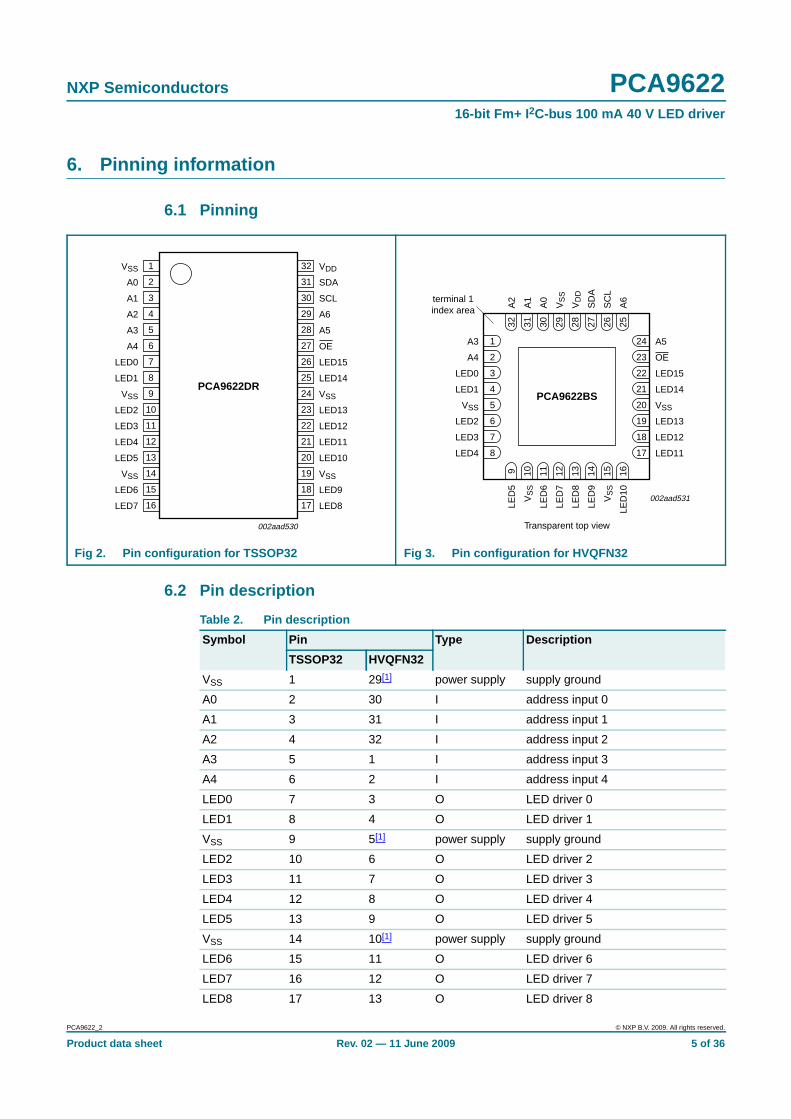
6. Pinning information
6.1 Pinning
6.2 Pin description
Fig 2. Pin configuration for TSSOP32 Fig 3. Pin configuration for HVQFN32
VDD
SDA
SCL
A6
A5
OE
LED15
LED14
VSS
LED13
LED12
LED11
LED10
VSS
LED9
LED8
VSS
A0
A1
A2
A3
A4
LED0
LED1
VSS
LED2
LED3
LED4
LED5
VSS
LED6
LED7
PCA9622DR
002aad530
1
2
3
4
5
6
7
8
9
10
11
12
13
14
15
16
18
17
20
19
22
21
24
23
26
25
32
31
30
29
28
27
002aad531
PCA9622BS
Transparent top view
LED11
LED3
LED4
LED12
LED2 LED13
VSS VSS
LED1 LED14
LED0 LED15
A4 OE
A3 A5
LED
5
VS
S
LED
6
LED
7
LED
8
LED
9
VS
S
LED
10
A2
A1
A0
VS
S
VD
D
SD
A
SC
L
A6
8 17
7 18
6 19
5 20
4 21
3 22
2 23
1 24
9 10 11 12 13 14 15 16
32 31 30 29 28 27 26 25
terminal 1index area
Table 2. Pin description
Symbol Pin Type Description
TSSOP32 HVQFN32
VSS 1 29[1] power supply supply ground
A0 2 30 I address input 0
A1 3 31 I address input 1
A2 4 32 I address input 2
A3 5 1 I address input 3
A4 6 2 I address input 4
LED0 7 3 O LED driver 0
LED1 8 4 O LED driver 1
VSS 9 5[1] power supply supply ground
LED2 10 6 O LED driver 2
LED3 11 7 O LED driver 3
LED4 12 8 O LED driver 4
LED5 13 9 O LED driver 5
VSS 14 10[1] power supply supply ground
LED6 15 11 O LED driver 6
LED7 16 12 O LED driver 7
LED8 17 13 O LED driver 8
PCA9622_2 © NXP B.V. 2009. All rights reserved.
Product data sheet Rev. 02 — 11 June 2009 5 of 36

NXP Semiconductors PCA962216-bit Fm+ I 2C-bus 100 mA 40 V LED driver
[1] HVQFN32 package supply ground is connected to both VSS pins and exposed center pad. VSS pins mustbe connected to supply ground for proper device operation. For enhanced thermal, electrical, and boardlevel performance, the exposed pad needs to be soldered to the board using a corresponding thermal padon the board and for proper heat conduction through the board, thermal vias need to be incorporated in thePCB in the thermal pad region.
LED9 18 14 O LED driver 9
VSS 19 15[1] power supply supply ground
LED10 20 16 O LED driver 10
LED11 21 17 O LED driver 11
LED12 22 18 O LED driver 12
LED13 23 19 O LED driver 12
VSS 24 20[1] power supply supply ground
LED14 25 21 O LED driver 14
LED15 26 22 O LED driver 15
OE 27 23 I active LOW output enable
A5 28 24 I address input 5
A6 29 25 I address input 6
SCL 30 26 I serial clock line
SDA 31 27 I/O serial data line
VDD 32 28 power supply supply voltage
Table 2. Pin description …continued
Symbol Pin Type Description
TSSOP32 HVQFN32
PCA9622_2 © NXP B.V. 2009. All rights reserved.
Product data sheet Rev. 02 — 11 June 2009 6 of 36
NXP Semiconductors PCA962216-bit Fm+ I 2C-bus 100 mA 40 V LED driver
7. Functional description
Refer to Figure 1 “Block diagram of PCA9622”.
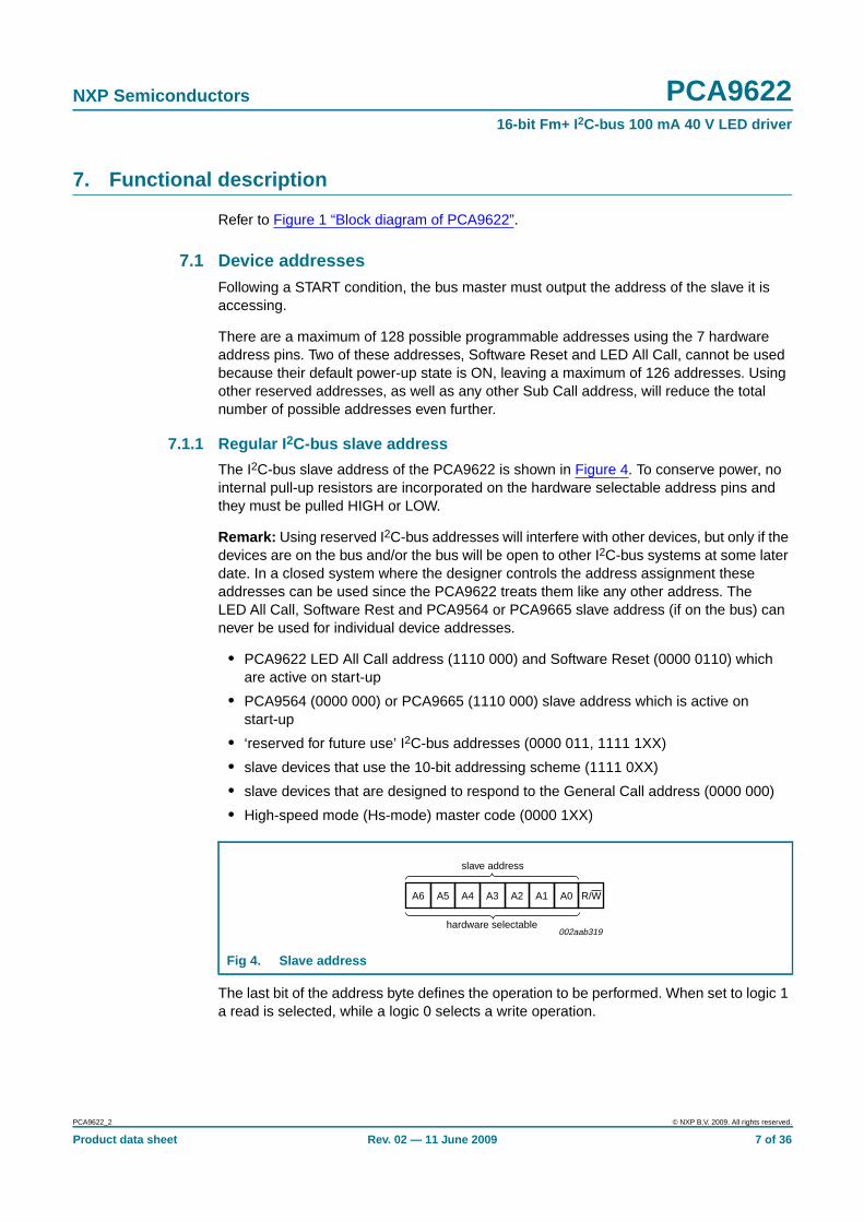
7.1 Device addressesFollowing a START condition, the bus master must output the address of the slave it isaccessing.
There are a maximum of 128 possible programmable addresses using the 7 hardwareaddress pins. Two of these addresses, Software Reset and LED All Call, cannot be usedbecause their default power-up state is ON, leaving a maximum of 126 addresses. Usingother reserved addresses, as well as any other Sub Call address, will reduce the totalnumber of possible addresses even further.
7.1.1 Regular I 2C-bus slave address
The I2C-bus slave address of the PCA9622 is shown in Figure 4. To conserve power, nointernal pull-up resistors are incorporated on the hardware selectable address pins andthey must be pulled HIGH or LOW.
Remark: Using reserved I2C-bus addresses will interfere with other devices, but only if thedevices are on the bus and/or the bus will be open to other I2C-bus systems at some laterdate. In a closed system where the designer controls the address assignment theseaddresses can be used since the PCA9622 treats them like any other address. TheLED All Call, Software Rest and PCA9564 or PCA9665 slave address (if on the bus) cannever be used for individual device addresses.
• PCA9622 LED All Call address (1110 000) and Software Reset (0000 0110) whichare active on start-up
• PCA9564 (0000 000) or PCA9665 (1110 000) slave address which is active onstart-up
• ‘reserved for future use’ I2C-bus addresses (0000 011, 1111 1XX)
• slave devices that use the 10-bit addressing scheme (1111 0XX)
• slave devices that are designed to respond to the General Call address (0000 000)
• High-speed mode (Hs-mode) master code (0000 1XX)
The last bit of the address byte defines the operation to be performed. When set to logic 1a read is selected, while a logic 0 selects a write operation.
Fig 4. Slave address
R/W
002aab319
A6 A5 A4 A3 A2 A1 A0
hardware selectable
slave address
PCA9622_2 © NXP B.V. 2009. All rights reserved.
Product data sheet Rev. 02 — 11 June 2009 7 of 36
NXP Semiconductors PCA962216-bit Fm+ I 2C-bus 100 mA 40 V LED driver
7.1.2 LED All Call I 2C-bus address
• Default power-up value (ALLCALLADR register): E0h or 1110 000
• Programmable through I2C-bus (volatile programming)
• At power-up, LED All Call I2C-bus address is enabled. PCA9622 sends an ACK whenE0h (R/W = 0) or E1h (R/W = 1) is sent by the master.
See Section 7.3.8 “ALLCALLADR, LED All Call I2C-bus address” for more detail.
Remark: The default LED All Call I2C-bus address (E0h or 1110 000) must not be usedas a regular I2C-bus slave address since this address is enabled at power-up. All thePCA9622s on the I2C-bus will acknowledge the address if sent by the I2C-bus master.
7.1.3 LED Sub Call I 2C-bus addresses
• 3 different I2C-bus addresses can be used
• Default power-up values:
– SUBADR1 register: E2h or 1110 001
– SUBADR2 register: E4h or 1110 010
– SUBADR3 register: E8h or 1110 100
• Programmable through I2C-bus (volatile programming)
• At power-up, Sub Call I2C-bus addresses are disabled. PCA9622 does not send anACK when E2h (R/W = 0) or E3h (R/W = 1), E4h (R/W = 0) or E5h (R/W = 1), orE8h (R/W = 0) or E9h (R/W = 1) is sent by the master.
See Section 7.3.7 “SUBADR1 to SUBADR3, I2C-bus subaddress 1 to 3” for more detail.
Remark: The default LED Sub Call I2C-bus addresses may be used as regular I2C-busslave addresses as long as they are disabled.
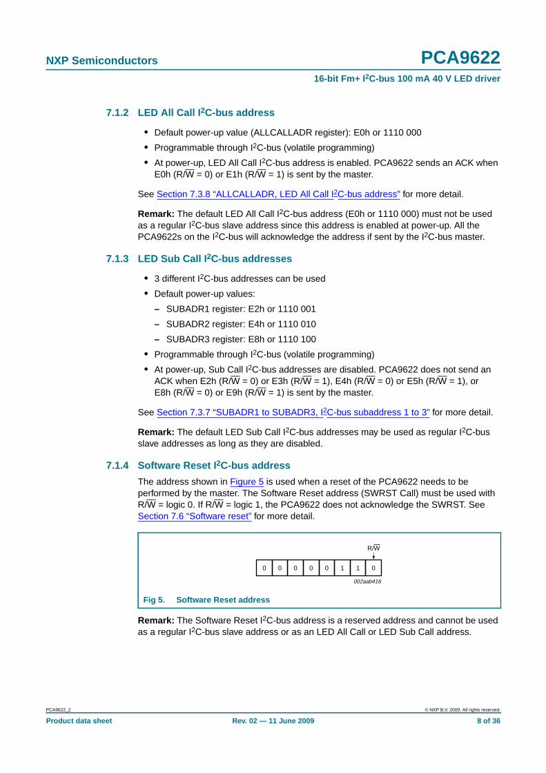
7.1.4 Software Reset I 2C-bus address
The address shown in Figure 5 is used when a reset of the PCA9622 needs to beperformed by the master. The Software Reset address (SWRST Call) must be used withR/W = logic 0. If R/W = logic 1, the PCA9622 does not acknowledge the SWRST. SeeSection 7.6 “Software reset” for more detail.
Remark: The Software Reset I2C-bus address is a reserved address and cannot be usedas a regular I2C-bus slave address or as an LED All Call or LED Sub Call address.
Fig 5. Software Reset address
0
002aab416
0 0 0 0 0 1 1
R/W
PCA9622_2 © NXP B.V. 2009. All rights reserved.
Product data sheet Rev. 02 — 11 June 2009 8 of 36
NXP Semiconductors PCA962216-bit Fm+ I 2C-bus 100 mA 40 V LED driver
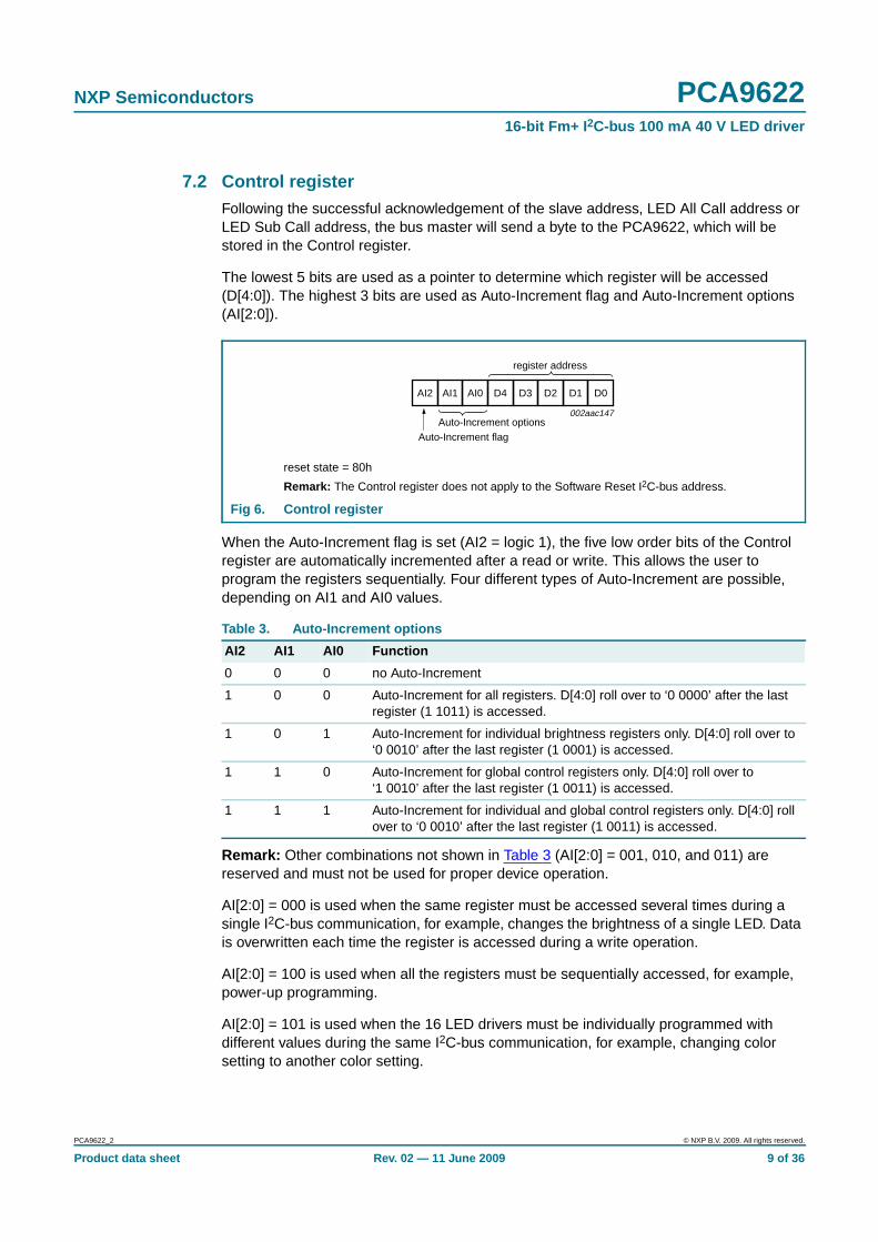
7.2 Control registerFollowing the successful acknowledgement of the slave address, LED All Call address orLED Sub Call address, the bus master will send a byte to the PCA9622, which will bestored in the Control register.
The lowest 5 bits are used as a pointer to determine which register will be accessed(D[4:0]). The highest 3 bits are used as Auto-Increment flag and Auto-Increment options(AI[2:0]).
When the Auto-Increment flag is set (AI2 = logic 1), the five low order bits of the Controlregister are automatically incremented after a read or write. This allows the user toprogram the registers sequentially. Four different types of Auto-Increment are possible,depending on AI1 and AI0 values.
Remark: Other combinations not shown in Table 3 (AI[2:0] = 001, 010, and 011) arereserved and must not be used for proper device operation.
AI[2:0] = 000 is used when the same register must be accessed several times during asingle I2C-bus communication, for example, changes the brightness of a single LED. Datais overwritten each time the register is accessed during a write operation.
AI[2:0] = 100 is used when all the registers must be sequentially accessed, for example,power-up programming.
AI[2:0] = 101 is used when the 16 LED drivers must be individually programmed withdifferent values during the same I2C-bus communication, for example, changing colorsetting to another color setting.
reset state = 80h
Remark: The Control register does not apply to the Software Reset I2C-bus address.
Fig 6. Control register
Table 3. Auto-Increment options
AI2 AI1 AI0 Function
0 0 0 no Auto-Increment
1 0 0 Auto-Increment for all registers. D[4:0] roll over to ‘0 0000’ after the lastregister (1 1011) is accessed.
1 0 1 Auto-Increment for individual brightness registers only. D[4:0] roll over to‘0 0010’ after the last register (1 0001) is accessed.
1 1 0 Auto-Increment for global control registers only. D[4:0] roll over to‘1 0010’ after the last register (1 0011) is accessed.
1 1 1 Auto-Increment for individual and global control registers only. D[4:0] rollover to ‘0 0010’ after the last register (1 0011) is accessed.
002aac147
AI2 AI1 AI0 D4 D3 D2 D1 D0
Auto-Increment flag
register address
Auto-Increment options
PCA9622_2 © NXP B.V. 2009. All rights reserved.
Product data sheet Rev. 02 — 11 June 2009 9 of 36

NXP Semiconductors PCA962216-bit Fm+ I 2C-bus 100 mA 40 V LED driver
AI[2:0] = 110 is used when the LED drivers must be globally programmed with differentsettings during the same I2C-bus communication, for example, global brightness orblinking change.
AI[2:0] = 111 is used when individual and global changes must be performed during thesame I2C-bus communication, for example, changing a color and global brightness at thesame time.
Only the 5 least significant bits D[4:0] are affected by the AI[2:0] bits.
When the Control register is written, the register entry point determined by D[4:0] is thefirst register that will be addressed (read or write operation), and can be anywherebetween 0 0000 and 1 1011 (as defined in Table 4). When AI[2] = 1, the Auto-Incrementflag is set and the rollover value at which the register increment stops and goes to the nextone is determined by AI[2:0]. See Table 3 for rollover values. For example, if the Controlregister = 1111 0100 (F4h), then the register addressing sequence will be (in hex):14 → … → 1B → 00 → … → 13 → 02 → … → 13 → 02 → … → 13 → 02 → … as longas the master keeps sending or reading data.
7.3 Register definitions
Table 4. Register summary [1] [2]
Register number (hex) D4 D3 D2 D1 D0 Name Type Function
00 0 0 0 0 0 MODE1 read/write Mode register 1
01 0 0 0 0 1 MODE2 read/write Mode register 2
02 0 0 0 1 0 PWM0 read/write brightness control LED0
03 0 0 0 1 1 PWM1 read/write brightness control LED1
04 0 0 1 0 0 PWM2 read/write brightness control LED2
05 0 0 1 0 1 PWM3 read/write brightness control LED3
06 0 0 1 1 0 PWM4 read/write brightness control LED4
07 0 0 1 1 1 PWM5 read/write brightness control LED5
08 0 1 0 0 0 PWM6 read/write brightness control LED6
09 0 1 0 0 1 PWM7 read/write brightness control LED7
0A 0 1 0 1 0 PWM8 read/write brightness control LED8
0B 0 1 0 1 1 PWM9 read/write brightness control LED9
0C 0 1 1 0 0 PWM10 read/write brightness control LED10
0D 0 1 1 0 1 PWM11 read/write brightness control LED11
0E 0 1 1 1 0 PWM12 read/write brightness control LED12
0F 0 1 1 1 1 PWM13 read/write brightness control LED13
10 1 0 0 0 0 PWM14 read/write brightness control LED14
11 1 0 0 0 1 PWM15 read/write brightness control LED15
12 1 0 0 1 0 GRPPWM read/write group duty cycle control
13 1 0 0 1 1 GRPFREQ read/write group frequency
14 1 0 1 0 0 LEDOUT0 read/write LED output state 0
15 1 0 1 0 1 LEDOUT1 read/write LED output state 1
16 1 0 1 1 0 LEDOUT2 read/write LED output state 2
17 1 0 1 1 1 LEDOUT3 read/write LED output state 3
PCA9622_2 © NXP B.V. 2009. All rights reserved.
Product data sheet Rev. 02 — 11 June 2009 10 of 36

NXP Semiconductors PCA962216-bit Fm+ I 2C-bus 100 mA 40 V LED driver
[1] Only D[4:0] = 0 0000 to 1 1011 are allowed and will be acknowledged. D[4:0] = 1 1100 to 1 1111 are reserved and will not beacknowledged.
[2] When writing to the Control register, bit 4 must be programmed with logic 0 for proper device operation.
7.3.1 Mode register 1, MODE1
[1] It takes 500 µs max. for the oscillator to be up and running once SLEEP bit has been set to logic 1. Timings on LEDn outputs are notguaranteed if PWMx, GRPPWM or GRPFREQ registers are accessed within the 500 µs window.
[2] No blinking or dimming is possible when the oscillator is off.
18 1 1 0 0 0 SUBADR1 read/write I2C-bus subaddress 1
19 1 1 0 0 1 SUBADR2 read/write I2C-bus subaddress 2
1A 1 1 0 1 0 SUBADR3 read/write I2C-bus subaddress 3
1B 1 1 0 1 1 ALLCALLADR read/write LED All Call I2C-bus address
Table 4. Register summary [1] [2] …continued
Register number (hex) D4 D3 D2 D1 D0 Name Type Function
Table 5. MODE1 - Mode register 1 (address 00h) bit descriptionLegend: * default value.
Bit Symbol Access Value Description
7 AI2 read only 0 Register Auto-Increment disabled.
1* Register Auto-Increment enabled.
6 AI1 read only 0* Auto-Increment bit 1 = 0.
1 Auto-Increment bit 1 = 1.
5 AI0 read only 0* Auto-Increment bit 0 = 0.
1 Auto-Increment bit 0 = 1.
4 SLEEP R/W 0 Normal mode[1].
1* Low power mode. Oscillator off[2].
3 SUB1 R/W 0* PCA9622 does not respond to I2C-bus subaddress 1.
1 PCA9622 responds to I2C-bus subaddress 1.
2 SUB2 R/W 0* PCA9622 does not respond to I2C-bus subaddress 2.
1 PCA9622 responds to I2C-bus subaddress 2.
1 SUB3 R/W 0* PCA9622 does not respond to I2C-bus subaddress 3.
1 PCA9622 responds to I2C-bus subaddress 3.
0 ALLCALL R/W 0 PCA9622 does not respond to LED All Call I2C-bus address.
1* PCA9622 responds to LED All Call I2C-bus address.
PCA9622_2 © NXP B.V. 2009. All rights reserved.
Product data sheet Rev. 02 — 11 June 2009 11 of 36

NXP Semiconductors PCA962216-bit Fm+ I 2C-bus 100 mA 40 V LED driver
7.3.2 Mode register 2, MODE2
[1] Change of the outputs at the STOP command allows synchronizing outputs of more than one PCA9622. Applicable to registers from02h (PWM0) to 17h (LEDOUT) only.
7.3.3 PWM0 to PWM15, individual brightness control
A 97 kHz fixed frequency signal is used for each output. Duty cycle is controlled through256 linear steps from 00h (0 % duty cycle = LED output off) to FFh(99.6 % duty cycle = LED output at maximum brightness). Applicable to LED outputsprogrammed with LDRx = 10 or 11 (LEDOUT0 to LEDOUT3 registers).
(1)
Table 6. MODE2 - Mode register 2 (address 01h) bit descriptionLegend: * default value.
Bit Symbol Access Value Description
7 - read only 0* reserved
6 - read only 0* reserved
5 DMBLNK R/W 0* group control = dimming
1 group control = blinking
4 INVRT R/W 0* reserved; write must always be a logic 0
3 OCH R/W 0* outputs change on STOP command[1]
1 outputs change on ACK
2 - R/W 1* reserved; write must always be a logic 1
1 - R/W 0* reserved; write must always be a logic 0
0 - R/W 1* reserved; write must always be a logic 1
Table 7. PWM0 to PWM15 - PWM registers 0 to 15 (address 02h to 11h) bit descriptionLegend: * default value.
Address Register Bit Symbol Access Value Description
02h PWM0 7:0 IDC0[7:0] R/W 0000 0000* PWM0 Individual Duty Cycle
03h PWM1 7:0 IDC1[7:0] R/W 0000 0000* PWM1 Individual Duty Cycle
04h PWM2 7:0 IDC2[7:0] R/W 0000 0000* PWM2 Individual Duty Cycle
05h PWM3 7:0 IDC3[7:0] R/W 0000 0000* PWM3 Individual Duty Cycle
06h PWM4 7:0 IDC4[7:0] R/W 0000 0000* PWM4 Individual Duty Cycle
07h PWM5 7:0 IDC5[7:0] R/W 0000 0000* PWM5 Individual Duty Cycle
08h PWM6 7:0 IDC6[7:0] R/W 0000 0000* PWM6 Individual Duty Cycle
09h PWM7 7:0 IDC7[7:0] R/W 0000 0000* PWM7 Individual Duty Cycle
0Ah PWM8 7:0 IDC8[7:0] R/W 0000 0000* PWM8 Individual Duty Cycle
0Bh PWM9 7:0 IDC9[7:0] R/W 0000 0000* PWM9 Individual Duty Cycle
0Ch PWM10 7:0 IDC10[7:0] R/W 0000 0000* PWM10 Individual Duty Cycle
0Dh PWM11 7:0 IDC11[7:0] R/W 0000 0000* PWM11 Individual Duty Cycle
0Eh PWM12 7:0 IDC12[7:0] R/W 0000 0000* PWM12 Individual Duty Cycle
0Fh PWM13 7:0 IDC13[7:0] R/W 0000 0000* PWM13 Individual Duty Cycle
10h PWM14 7:0 IDC14[7:0] R/W 0000 0000* PWM14 Individual Duty Cycle
11h PWM15 7:0 IDC15[7:0] R/W 0000 0000* PWM15 Individual Duty Cycle
duty cycleIDCx 7:0[ ]
256---------------------------=
PCA9622_2 © NXP B.V. 2009. All rights reserved.
Product data sheet Rev. 02 — 11 June 2009 12 of 36

NXP Semiconductors PCA962216-bit Fm+ I 2C-bus 100 mA 40 V LED driver
7.3.4 GRPPWM, group duty cycle control
When DMBLNK bit (MODE2 register) is programmed with logic 0, a 190 Hz fixedfrequency signal is superimposed with the 97 kHz individual brightness control signal.GRPPWM is then used as a global brightness control allowing the LED outputs to bedimmed with the same value. The value in GRPFREQ is then a ‘Don’t care’.
General brightness for the 16 outputs is controlled through 256 linear steps from 00h(0 % duty cycle = LED output off) to FFh (99.6 % duty cycle = maximum brightness).Applicable to LED outputs programmed with LDRx = 11 (LEDOUT0 to LEDOUT3registers).
When DMBLNK bit is programmed with logic 1, GRPPWM and GRPFREQ registersdefine a global blinking pattern, where GRPFREQ contains the blinking period (from24 Hz to 10.73 s) and GRPPWM the duty cycle (ON/OFF ratio in %).
(2)
7.3.5 GRPFREQ, group frequency
GRPFREQ is used to program the global blinking period when DMBLNK bit (MODE2register) is equal to 1. Value in this register is a ‘Don’t care’ when DMBLNK = 0.Applicable to LED outputs programmed with LDRx = 11 (LEDOUT0 to LEDOUT3registers).
Blinking period is controlled through 256 linear steps from 00h (41 ms, frequency 24 Hz)to FFh (10.73 s).
(3)
Table 8. GRPPWM - Group brightness control register (address 12h) bit descriptionLegend: * default value
Address Register Bit Symbol Access Value Description
12h GRPPWM 7:0 GDC[7:0] R/W 1111 1111 GRPPWM register
duty cycleGDC 7:0[ ]
256---------------------------=
Table 9. GRPFREQ - Group Frequency register (address 13h) bit descriptionLegend: * default value.
Address Register Bit Symbol Access Value Description
13h GRPFREQ 7:0 GFRQ[7:0] R/W 0000 0000* GRPFREQ register
global blinking periodGFRQ 7:0[ ] 1+
24---------------------------------------- s( )=
PCA9622_2 © NXP B.V. 2009. All rights reserved.
Product data sheet Rev. 02 — 11 June 2009 13 of 36

NXP Semiconductors PCA962216-bit Fm+ I 2C-bus 100 mA 40 V LED driver
7.3.6 LEDOUT0 to LEDOUT3, LED driver output state
LDRx = 00 — LED driver x is off (default power-up state).
LDRx = 01 — LED driver x is fully on (individual brightness and group dimming/blinkingnot controlled).
LDRx = 10 — LED driver x individual brightness can be controlled through its PWMxregister.
LDRx = 11 — LED driver x individual brightness and group dimming/blinking can becontrolled through its PWMx register and the GRPPWM registers.
7.3.7 SUBADR1 to SUBADR3, I 2C-bus subaddress 1 to 3
Subaddresses are programmable through the I2C-bus. Default power-up values are E2h,E4h, E8h, and the device(s) will not acknowledge these addresses right after power-up(the corresponding SUBx bit in MODE1 register is equal to 0).
Table 10. LEDOUT0 to LEDOUT3 - LED driver output state register (address 14h to 17h)bit description
Legend: * default value.
Address Register Bit Symbol Access Value Description
14h LEDOUT0 7:6 LDR3 R/W 00* LED3 output state control
5:4 LDR2 R/W 00* LED2 output state control
3:2 LDR1 R/W 00* LED1 output state control
1:0 LDR0 R/W 00* LED0 output state control
15h LEDOUT1 7:6 LDR7 R/W 00* LED7 output state control
5:4 LDR6 R/W 00* LED6 output state control
3:2 LDR5 R/W 00* LED5 output state control
1:0 LDR4 R/W 00* LED4 output state control
16h LEDOUT2 7:6 LDR11 R/W 00* LED11 output state control
5:4 LDR10 R/W 00* LED10 output state control
3:2 LDR9 R/W 00* LED9 output state control
1:0 LDR8 R/W 00* LED8 output state control
17h LEDOUT3 7:6 LDR15 R/W 00* LED15 output state control
5:4 LDR14 R/W 00* LED14 output state control
3:2 LDR13 R/W 00* LED13 output state control
1:0 LDR12 R/W 00* LED12 output state control
Table 11. SUBADR1 to SUBADR3 - I 2C-bus subaddress registers 0 to 3 (address 18h to1Ah) bit description
Legend: * default value.
Address Register Bit Symbol Access Value Description
18h SUBADR1 7:1 A1[7:1] R/W 1110 001* I2C-bus subaddress 1
0 A1[0] R only 0* reserved
19h SUBADR2 7:1 A2[7:1] R/W 1110 010* I2C-bus subaddress 2
0 A2[0] R only 0* reserved
1Ah SUBADR3 7:1 A3[7:1] R/W 1110 100* I2C-bus subaddress 3
0 A3[0] R only 0* reserved
PCA9622_2 © NXP B.V. 2009. All rights reserved.
Product data sheet Rev. 02 — 11 June 2009 14 of 36

NXP Semiconductors PCA962216-bit Fm+ I 2C-bus 100 mA 40 V LED driver
Once subaddresses have been programmed to their right values, SUBx bits need to beset to logic 1 in order to have the device acknowledging these addresses (MODE1register).
Only the 7 MSBs representing the I2C-bus subaddress are valid. The LSB in SUBADRxregister is a read-only bit (0).
When SUBx is set to logic 1, the corresponding I2C-bus subaddress can be used duringeither an I2C-bus read or write sequence.
7.3.8 ALLCALLADR, LED All Call I 2C-bus address
The LED All Call I2C-bus address allows all the PCA9622s on the bus to be programmedat the same time (ALLCALL bit in register MODE1 must be equal to 1 (power-up defaultstate)). This address is programmable through the I2C-bus and can be used during eitheran I2C-bus read or write sequence. The register address can also be programmed as aSub Call.
Only the 7 MSBs representing the All Call I2C-bus address are valid. The LSB inALLCALLADR register is a read-only bit (0).
If ALLCALL bit = 0, the device does not acknowledge the address programmed in registerALLCALLADR.
7.4 Active LOW output enable inputThe active LOW output enable (OE) pin, allows to enable or disable all the LED outputs atthe same time.
• When a LOW level is applied to OE pin, all the LED outputs are enabled.
• When a HIGH level is applied to OE pin, all the LED outputs are high-impedance.
The OE pin can be used as a synchronization signal to switch on/off several PCA9622devices at the same time. This requires an external clock reference that provides blinkingperiod and the duty cycle.
The OE pin can also be used as an external dimming control signal. The frequency of theexternal clock must be high enough not to be seen by the human eye, and the duty cyclevalue determines the brightness of the LEDs.
Remark: Do not use OE as an external blinking control signal when internal globalblinking is selected (DMBLNK = 1, MODE2 register) since it will result in an undefinedblinking pattern. Do not use OE as an external dimming control signal when internal globaldimming is selected (DMBLNK = 0, MODE2 register) since it will result in an undefineddimming pattern.
Table 12. ALLCALLADR - LED All Call I 2C-bus address register (address 1Bh) bitdescription
Legend: * default value.
Address Register Bit Symbol Access Value Description
1Bh ALLCALLADR 7:1 AC[7:1] R/W 1110 000* ALLCALL I2C-busaddress register
0 AC[0] R only 0* reserved
PCA9622_2 © NXP B.V. 2009. All rights reserved.
Product data sheet Rev. 02 — 11 June 2009 15 of 36

NXP Semiconductors PCA962216-bit Fm+ I 2C-bus 100 mA 40 V LED driver
7.5 Power-on resetWhen power is applied to VDD, an internal power-on reset holds the PCA9622 in a resetcondition until VDD has reached VPOR. At this point, the reset condition is released and thePCA9622 registers and I2C-bus state machine are initialized to their default states (allzeroes) causing all the channels to be deselected. Thereafter, VDD must be lowered below0.2 V to reset the device.
7.6 Software resetThe Software Reset Call (SWRST Call) allows all the devices in the I2C-bus to be reset tothe power-up state value through a specific formatted I2C-bus command. To be performedcorrectly, it implies that the I2C-bus is functional and that there is no device hanging thebus.
The SWRST Call function is defined as the following:
1. A START command is sent by the I2C-bus master.
2. The reserved SWRST I2C-bus address ‘0000 011’ with the R/W bit set to ‘0’ (write) issent by the I2C-bus master.
3. The PCA9622 device(s) acknowledge(s) after seeing the SWRST Call address‘0000 0110’ (06h) only. If the R/W bit is set to ‘1’ (read), no acknowledge is returned tothe I2C-bus master.
4. Once the SWRST Call address has been sent and acknowledged, the master sends2 bytes with 2 specific values (SWRST data byte 1 and byte 2):
a. Byte 1 = A5h: the PCA9622 acknowledges this value only. If byte 1 is not equal toA5h, the PCA9622 does not acknowledge it.
b. Byte 2 = 5Ah: the PCA9622 acknowledges this value only. If byte 2 is not equal to5Ah, then the PCA9622 does not acknowledge it.
If more than 2 bytes of data are sent, the PCA9622 does not acknowledge any more.
5. Once the right 2 bytes (SWRST data byte 1 and byte 2 only) have been sent andcorrectly acknowledged, the master sends a STOP command to end the SWRST Call:the PCA9622 then resets to the default value (power-up value) and is ready to beaddressed again within the specified bus free time (tBUF).
The I2C-bus master must interpret a non-acknowledge from the PCA9622 (at any time) asa ‘SWRST Call Abort’. The PCA9622 does not initiate a reset of its registers. Thishappens only when the format of the SWRST Call sequence is not correct.
PCA9622_2 © NXP B.V. 2009. All rights reserved.
Product data sheet Rev. 02 — 11 June 2009 16 of 36
NXP Semiconductors PCA962216-bit Fm+ I 2C-bus 100 mA 40 V LED driver
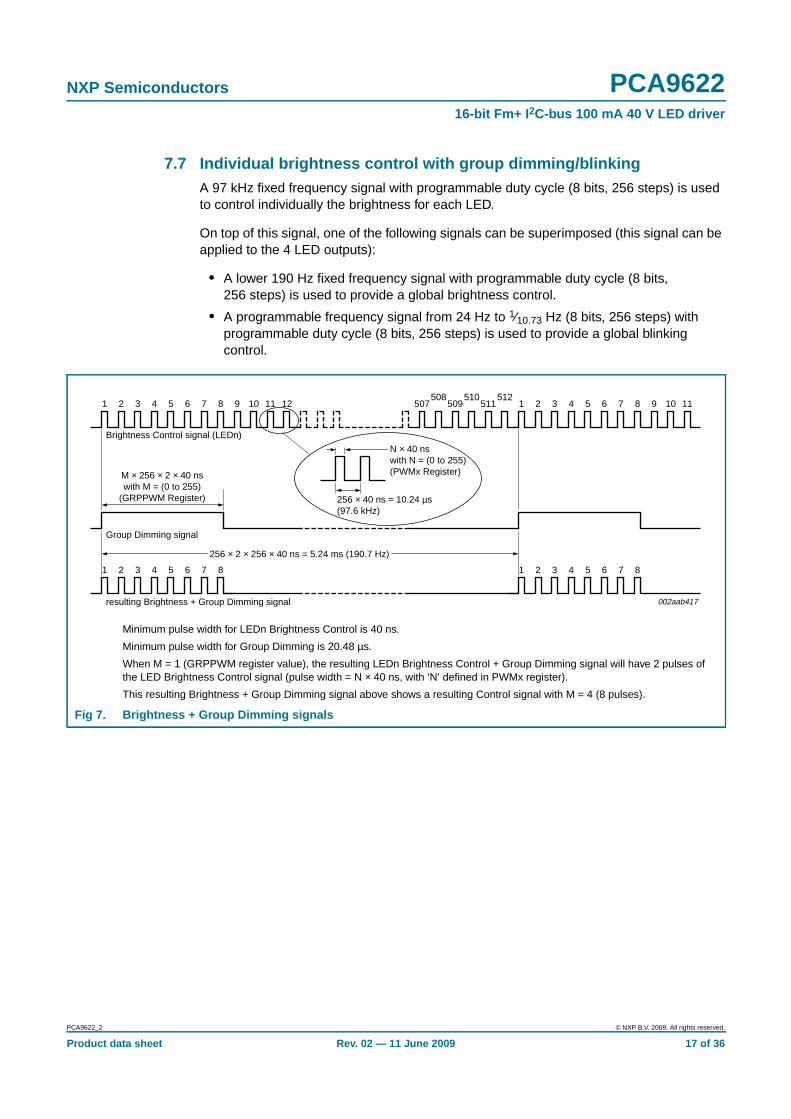
7.7 Individual brightness control with group dimming/blinkingA 97 kHz fixed frequency signal with programmable duty cycle (8 bits, 256 steps) is usedto control individually the brightness for each LED.
On top of this signal, one of the following signals can be superimposed (this signal can beapplied to the 4 LED outputs):
• A lower 190 Hz fixed frequency signal with programmable duty cycle (8 bits,256 steps) is used to provide a global brightness control.
• A programmable frequency signal from 24 Hz to 1⁄10.73 Hz (8 bits, 256 steps) withprogrammable duty cycle (8 bits, 256 steps) is used to provide a global blinkingcontrol.
Minimum pulse width for LEDn Brightness Control is 40 ns.
Minimum pulse width for Group Dimming is 20.48 µs.
When M = 1 (GRPPWM register value), the resulting LEDn Brightness Control + Group Dimming signal will have 2 pulses ofthe LED Brightness Control signal (pulse width = N × 40 ns, with ‘N’ defined in PWMx register).
This resulting Brightness + Group Dimming signal above shows a resulting Control signal with M = 4 (8 pulses).
Fig 7. Brightness + Group Dimming signals
1 2 3 4 5 6 7 8 9 10 11 12 507508
509510
511512
1 2 3 4 5 6 7 8 9 10 11
Brightness Control signal (LEDn)
M × 256 × 2 × 40 nswith M = (0 to 255)
(GRPPWM Register)
N × 40 nswith N = (0 to 255)(PWMx Register)
256 × 40 ns = 10.24 µs(97.6 kHz)
1 2 3 4 5 6 7 81 2 3 4 5 6 7 8
Group Dimming signal
resulting Brightness + Group Dimming signal
256 × 2 × 256 × 40 ns = 5.24 ms (190.7 Hz)
002aab417
PCA9622_2 © NXP B.V. 2009. All rights reserved.
Product data sheet Rev. 02 — 11 June 2009 17 of 36

NXP Semiconductors PCA962216-bit Fm+ I 2C-bus 100 mA 40 V LED driver
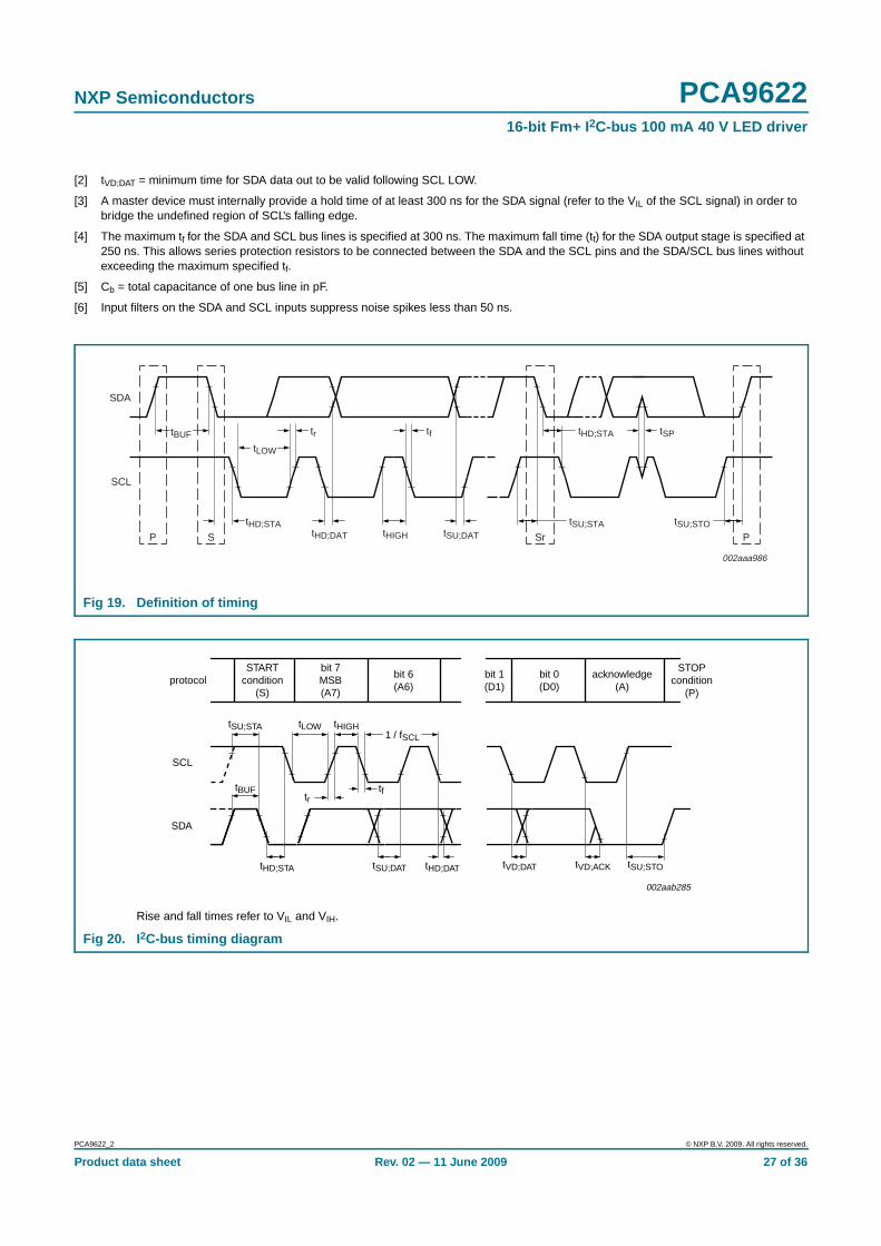
8. Characteristics of the I 2C-bus
The I2C-bus is for 2-way, 2-line communication between different ICs or modules. The twolines are a serial data line (SDA) and a serial clock line (SCL). Both lines must beconnected to a positive supply via a pull-up resistor when connected to the output stagesof a device. Data transfer may be initiated only when the bus is not busy.
8.1 Bit transferOne data bit is transferred during each clock pulse. The data on the SDA line must remainstable during the HIGH period of the clock pulse as changes in the data line at this timewill be interpreted as control signals (see Figure 8).
8.1.1 START and STOP conditions
Both data and clock lines remain HIGH when the bus is not busy. A HIGH-to-LOWtransition of the data line while the clock is HIGH is defined as the START condition (S). ALOW-to-HIGH transition of the data line while the clock is HIGH is defined as the STOPcondition (P) (see Figure 9).
8.2 System configurationA device generating a message is a ‘transmitter’; a device receiving is the ‘receiver’. Thedevice that controls the message is the ‘master’ and the devices which are controlled bythe master are the ‘slaves’ (see Figure 10).
Fig 8. Bit transfer
mba607
data linestable;
data valid
changeof dataallowed
SDA
SCL
Fig 9. Definition of START and STOP conditions
mba608
SDA
SCLP
STOP condition
S
START condition
PCA9622_2 © NXP B.V. 2009. All rights reserved.
Product data sheet Rev. 02 — 11 June 2009 18 of 36

NXP Semiconductors PCA962216-bit Fm+ I 2C-bus 100 mA 40 V LED driver
8.3 AcknowledgeThe number of data bytes transferred between the START and the STOP conditions fromtransmitter to receiver is not limited. Each byte of eight bits is followed by oneacknowledge bit. The acknowledge bit is a HIGH level put on the bus by the transmitter,whereas the master generates an extra acknowledge related clock pulse.
A slave receiver which is addressed must generate an acknowledge after the reception ofeach byte. Also a master must generate an acknowledge after the reception of each bytethat has been clocked out of the slave transmitter. The device that acknowledges has topull down the SDA line during the acknowledge clock pulse, so that the SDA line is stableLOW during the HIGH period of the acknowledge related clock pulse; set-up time and holdtime must be taken into account.
A master receiver must signal an end of data to the transmitter by not generating anacknowledge on the last byte that has been clocked out of the slave. In this event, thetransmitter must leave the data line HIGH to enable the master to generate a STOPcondition.
Fig 10. System configuration
002aaa966
MASTERTRANSMITTER/
RECEIVER
SLAVERECEIVER
SLAVETRANSMITTER/
RECEIVER
MASTERTRANSMITTER
MASTERTRANSMITTER/
RECEIVER
SDA
SCL
I2C-BUSMULTIPLEXER
SLAVE
Fig 11. Acknowledgement on the I 2C-bus
002aaa987
S
STARTcondition
9821
clock pulse foracknowledgement
not acknowledge
acknowledge
data outputby transmitter
data outputby receiver
SCL from master
PCA9622_2 © NXP B.V. 2009. All rights reserved.
Product data sheet Rev. 02 — 11 June 2009 19 of 36
NXP Semiconductors PCA962216-bit Fm+ I 2C-bus 100 mA 40 V LED driver
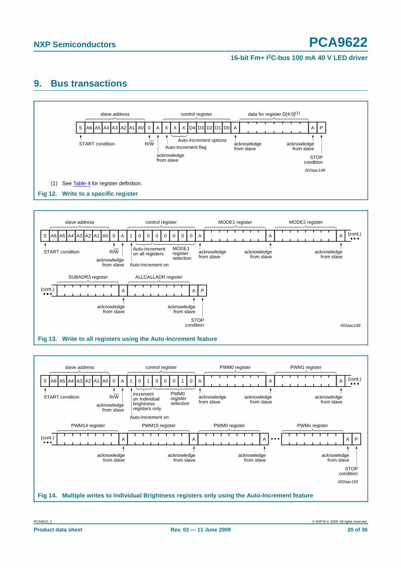
9. Bus transactions
(1) See Table 4 for register definition.
Fig 12. Write to a specific register
A5 A4 A3 A2 A1 A0 0 AS A6
slave address
START condition R/W
acknowledgefrom slave
002aac148
data for register D[4:0](1)
X X D4 D3 D2 D1 D0X
control register
Auto-Increment flag
Auto-Increment options
A
acknowledgefrom slave
A
acknowledgefrom slave
P
STOPcondition
Fig 13. Write to all registers using the Auto-Increment feature
A5 A4 A3 A2 A1 A0 0 AS A6
slave address
START condition R/W
acknowledgefrom slave
002aac149
MODE1 register
0 0 0 0 0 0 01
control register
Auto-Increment on
Auto-Incrementon all registers
A
acknowledgefrom slave
A
acknowledgefrom slave
P
STOPcondition
(cont.)
(cont.)
MODE1registerselection
MODE2 register
A
acknowledgefrom slave
SUBADR3 register
A
acknowledgefrom slave
ALLCALLADR register
A
acknowledgefrom slave
Fig 14. Multiple writes to Individual Brightness registers only using the Auto-Increment feature
A5 A4 A3 A2 A1 A0 0 AS A6
slave address
START condition R/W
acknowledgefrom slave
002aac150
PWM0 register
0 1 0 0 0 1 01
control register
Auto-Increment on
incrementon Individual brightness registers only
A
acknowledgefrom slave
A
acknowledgefrom slave
P
STOPcondition
(cont.)
(cont.)
PWM0registerselection
PWM1 register
A
acknowledgefrom slave
PWM14 register
A
acknowledgefrom slave
PWM15 register
A
acknowledgefrom slave
PWM0 register
A
acknowledgefrom slave
PWMx register
A
acknowledgefrom slave
PCA9622_2 © NXP B.V. 2009. All rights reserved.
Product data sheet Rev. 02 — 11 June 2009 20 of 36

NXP Semiconductors PCA962216-bit Fm+ I 2C-bus 100 mA 40 V LED driver
Fig 15. Read all registers using the Auto-Increment feature
A5 A4 A3 A2 A1 A0 0 AS A6
slave address
START condition R/W
acknowledgefrom slave
002aac151
0 0 0 0 0 0 01
control register
Auto-Increment on
Auto-Incrementon all registers
A
acknowledgefrom slave
(cont.)
(cont.)
MODE1registerselection
data from MODE1 register
A
acknowledgefrom master
Sr
ReSTARTcondition
A5 A4 A3 A2 A1 A0 1 AA6
slave address
R/W
acknowledgefrom slave
data from MODE2 register
A
acknowledgefrom master
data from PWM0
A
acknowledgefrom master
data fromALLCALLADR register
A
acknowledgefrom master
data fromMODE1 register
A
acknowledgefrom master
(cont.)
(cont.)
data from last read byte
A
not acknowledgefrom master
P
STOPcondition
(1) In this example, several PCA9622s are used and the same sequence (A) (above) is sent to each of them.
(2) ALLCALL bit in MODE1 register is equal to 1 for this example.
(3) OCH bit in MODE2 register is equal to 1 for this example.
Fig 16. LED All Call I 2C-bus address programming and LED All Call sequence example
A5 A4 A3 A2 A1 A0 0 AS A6
slave address(1)
START condition R/W
acknowledgefrom slave
002aac152
X X 1 1 0 1 1X
control register
Auto-Increment on
A
acknowledgefrom slave
ALLCALLADRregister selection
0 1 0 1 0 1 X1
new LED All Call I2C address(2)
P
STOPcondition
A
acknowledgefrom slave
0 1 0 1 0 1 0 AS 1
LED All Call I2C address
START condition R/W
acknowledgefrom the
4 devices
X X 0 1 0 0 0X
control register
A
acknowledgefrom the4 devices
LEDOUTregister selection
1 0 1 0 1 0 10
LEDOUT register (LED fully ON)
P
STOPcondition
A
acknowledgefrom the
4 devices
the 16 LEDs are on at the acknowledge(3)
sequence (A)
sequence (B)
PCA9622_2 © NXP B.V. 2009. All rights reserved.
Product data sheet Rev. 02 — 11 June 2009 21 of 36

NXP Semiconductors PCA962216-bit Fm+ I 2C-bus 100 mA 40 V LED driver
10. Application design-in information
(1) OE requires pull-up resistor if control signal from the master is open-drain.
I2C-bus address = 0010 101x.
Fig 17. Typical application
PCA9622
LED0
LED1
SDA
SCL
OE
VDD = 2.5 V, 3.3 V or 5.0 V
I2C-BUS/SMBusMASTER
SDA
SCL
10 kΩ
OE
10 kΩ
LED2
LED3
A0
A1
A2
VDD
A3
A4
A5
A6
VSS
10 kΩ(1)
up to 40 V
LED8
LED9
LED10
LED11
LED4
LED5
LED6
LED7
up to 40 VLED light bar
LED12
LED13
LED14
LED15
up to 40 VLED light bar
002aad532
VSS
up to 40 V
PCA9622_2 © NXP B.V. 2009. All rights reserved.
Product data sheet Rev. 02 — 11 June 2009 22 of 36

NXP Semiconductors PCA962216-bit Fm+ I 2C-bus 100 mA 40 V LED driver
11. Limiting values
[1] Each bit must be limited to a maximum of 100 mA and the total package limited to 1600 mA due to internalbusing limits.
Table 13. Limiting valuesIn accordance with the Absolute Maximum Rating System (IEC 60134).
Symbol Parameter Conditions Min Max Unit
VDD supply voltage −0.5 +6.0 V
VI/O voltage on an input/output pin VSS − 0.5 5.5 V
Vdrv(LED) LED driver voltage VSS − 0.5 40 V
IO(LEDn) output current on pin LEDn - 100 mA
IOL(tot) total LOW-level output current VOL = 0.5 V [1] 1600 - mA
ISS ground supply current per VSS pin - 800 mA
Ptot total power dissipation Tamb = 25 °C - 1.8 W
Tamb = 85 °C - 0.72 W
P/ch power dissipation per channel Tamb = 25 °C - 100 mW
Tamb = 85 °C - 45 mW
Tstg storage temperature −65 +150 °C
Tamb ambient temperature operating −40 +85 °C
PCA9622_2 © NXP B.V. 2009. All rights reserved.
Product data sheet Rev. 02 — 11 June 2009 23 of 36

NXP Semiconductors PCA962216-bit Fm+ I 2C-bus 100 mA 40 V LED driver
12. Static characteristics
[1] VDD must be lowered to 0.2 V in order to reset part.
[2] Each bit must be limited to a maximum of 100 mA and the total package limited to 1600 mA due to internal busing limits.
Table 14. Static characteristicsVDD = 2.3 V to 5.5 V; VSS = 0 V; Tamb = −40 °C to +85 °C; unless otherwise specified.
Symbol Parameter Conditions Min Typ Max Unit
Supply
VDD supply voltage 2.3 - 5.5 V
IDD supply current on pin VDD; operating mode;no load; fSCL = 1 MHz
VDD = 2.7 V - 0.2 4 mA
VDD = 3.6 V - 2 6 mA
VDD = 5.5 V - 8.5 12 mA
Istb standby current on pin VDD;no load; fSCL = 0 Hz;I/O = inputs; VI = VDD
VDD = 2.7 V - 1.3 5 µA
VDD = 3.6 V - 1.8 6 µA
VDD = 5.5 V - 3.2 7 µA
VPOR power-on reset voltage no load; VI = VDD or VSS[1] - 1.70 2.0 V
Input SCL; input/output SDA
VIL LOW-level input voltage −0.5 - +0.3VDD V
VIH HIGH-level input voltage 0.7VDD - 5.5 V
IOL LOW-level output current VOL = 0.4 V; VDD = 2.3 V 20 - - mA
VOL = 0.4 V; VDD = 5.0 V 30 - - mA
IL leakage current VI = VDD or VSS −1 - +1 µA
Ci input capacitance VI = VSS - 6 10 pF
LED driver outputs
Vdrv(LED) LED driver voltage 0 - 40 V
IOL LOW-level output current VOL = 0.5 V [2] 100 - - mA
Ron ON-state resistance Vdrv(LED) = 40 V; VDD = 2.3 V - 2 5 Ω
Co output capacitance - 2.5 5 pF
OE input
VIL LOW-level input voltage −0.5 - +0.3VDD V
VIH HIGH-level input voltage 0.7VDD - 5.5 V
ILI input leakage current −1 - +1 µA
Ci input capacitance - 15 40 pF
Address inputs
VIL LOW-level input voltage −0.5 - +0.3VDD V
VIH HIGH-level input voltage 0.7VDD - 5.5 V
ILI input leakage current −1 - +1 µA
Ci input capacitance - 3.7 5 pF
PCA9622_2 © NXP B.V. 2009. All rights reserved.
Product data sheet Rev. 02 — 11 June 2009 24 of 36

NXP Semiconductors PCA962216-bit Fm+ I 2C-bus 100 mA 40 V LED driver
a. Tamb = −40 °C b. Tamb = 25 °C
c. Tamb = 85 °C
Fig 18. VOL versus I OL
VOL (V)−0.05 0.550.350.15
002aae507
0.05
0.15
0.25
IOL(A)
−0.05
VDD = 5.5 V4.5 V3.0 V2.3 V
VOL (V)−0.05 0.550.350.15
002aae508
0.05
0.15
0.25
IOL(A)
−0.05
VDD = 5.5 V4.5 V3.0 V2.3 V
VOL (V)−0.05 0.550.350.15
002aae509
0.05
0.15
0.25
IOL(A)
−0.05
VDD = 5.5 V4.5 V3.0 V2.3 V
PCA9622_2 © NXP B.V. 2009. All rights reserved.
Product data sheet Rev. 02 — 11 June 2009 25 of 36

NXP Semiconductors PCA962216-bit Fm+ I 2C-bus 100 mA 40 V LED driver
13. Dynamic characteristics
[1] tVD;ACK = time for Acknowledgement signal from SCL LOW to SDA (out) LOW.
Table 15. Dynamic characteristics
Symbol Parameter Conditions Standard-modeI2C-bus
Fast-mode I 2C-bus Fast-modePlus I 2C-bus
Unit
Min Max Min Max Min Max
fSCL SCL clock frequency 0 100 0 400 0 1000 kHz
tBUF bus free time betweena STOP and STARTcondition
4.7 - 1.3 - 0.5 - µs
tHD;STA hold time (repeated)START condition
4.0 - 0.6 - 0.26 - µs
tSU;STA set-up time for arepeated STARTcondition
4.7 - 0.6 - 0.26 - µs
tSU;STO set-up time for STOPcondition
4.0 - 0.6 - 0.26 - µs
tHD;DAT data hold time 0 - 0 - 0 - ns
tVD;ACK data valid acknowledgetime
[1] 0.3 3.45 0.1 0.9 0.05 0.45 µs
tVD;DAT data valid time [2] 0.3 3.45 0.1 0.9 0.05 0.45 µs
tSU;DAT data set-up time 250 - 100 - 50 - ns
tLOW LOW period of the SCLclock
4.7 - 1.3 - 0.5 - µs
tHIGH HIGH period of theSCL clock
4.0 - 0.6 - 0.26 - µs
tf fall time of both SDAand SCL signals
[3][4] - 300 20 + 0.1Cb[5] 300 - 120 ns
tr rise time of both SDAand SCL signals
- 1000 20 + 0.1Cb[5] 300 - 120 ns
tSP pulse width of spikesthat must besuppressed by theinput filter
[6] - 50 - 50 - 50 ns
Output propagation delay
tPLH LOW to HIGHpropagation delay
OE to LEDn;MODE2[1:0] = 01
- - - - - 150 ns
tPHL HIGH to LOWpropagation delay
OE to LEDn;MODE2[1:0] = 01
- - - - - 150 ns
Output port timing
td(SCL-Q) delay time from SCLto data output
SCL to LEDn;MODE2[3] = 1;outputs change onACK
- - - - - 450 ns
td(SDA-Q) delay time from SDAto data output
SDA to LEDn;MODE2[3] = 0;outputs change onSTOP condition
- - - - - 450 ns
PCA9622_2 © NXP B.V. 2009. All rights reserved.
Product data sheet Rev. 02 — 11 June 2009 26 of 36
NXP Semiconductors PCA962216-bit Fm+ I 2C-bus 100 mA 40 V LED driver
[2] tVD;DAT = minimum time for SDA data out to be valid following SCL LOW.
[3] A master device must internally provide a hold time of at least 300 ns for the SDA signal (refer to the VIL of the SCL signal) in order tobridge the undefined region of SCL’s falling edge.
[4] The maximum tf for the SDA and SCL bus lines is specified at 300 ns. The maximum fall time (tf) for the SDA output stage is specified at250 ns. This allows series protection resistors to be connected between the SDA and the SCL pins and the SDA/SCL bus lines withoutexceeding the maximum specified tf.
[5] Cb = total capacitance of one bus line in pF.
[6] Input filters on the SDA and SCL inputs suppress noise spikes less than 50 ns.
Fig 19. Definition of timing
tSPtBUF
tHD;STA
PP S
tLOW
tr
tHD;DAT
tf
tHIGH tSU;DAT
tSU;STA
Sr
tHD;STA
tSU;STO
SDA
SCL
002aaa986
Rise and fall times refer to VIL and VIH.
Fig 20. I2C-bus timing diagram
SCL
SDA
tHD;STA tSU;DAT tHD;DAT
tftBUF
tSU;STA tLOW tHIGH
tVD;ACK
002aab285
tSU;STO
protocolSTART
condition(S)
bit 7MSB(A7)
bit 6(A6)
bit 1(D1)
bit 0(D0)
1 / fSCL
tr
tVD;DAT
acknowledge(A)
STOPcondition
(P)
PCA9622_2 © NXP B.V. 2009. All rights reserved.
Product data sheet Rev. 02 — 11 June 2009 27 of 36

NXP Semiconductors PCA962216-bit Fm+ I 2C-bus 100 mA 40 V LED driver
14. Test information
RL = Load resistor for LEDn. RL for SDA and SCL > 1 kΩ (3 mA or less current).
CL = Load capacitance includes jig and probe capacitance.
RT = Termination resistance should be equal to the output impedance Zo of the pulse generators.
Fig 21. Test circuitry for switching times
PULSEGENERATOR
VO
CL50 pF
RL500 Ω
002aab284
RT
VI
VDD
DUT
VDDopenGND
PCA9622_2 © NXP B.V. 2009. All rights reserved.
Product data sheet Rev. 02 — 11 June 2009 28 of 36
NXP Semiconductors PCA962216-bit Fm+ I 2C-bus 100 mA 40 V LED driver
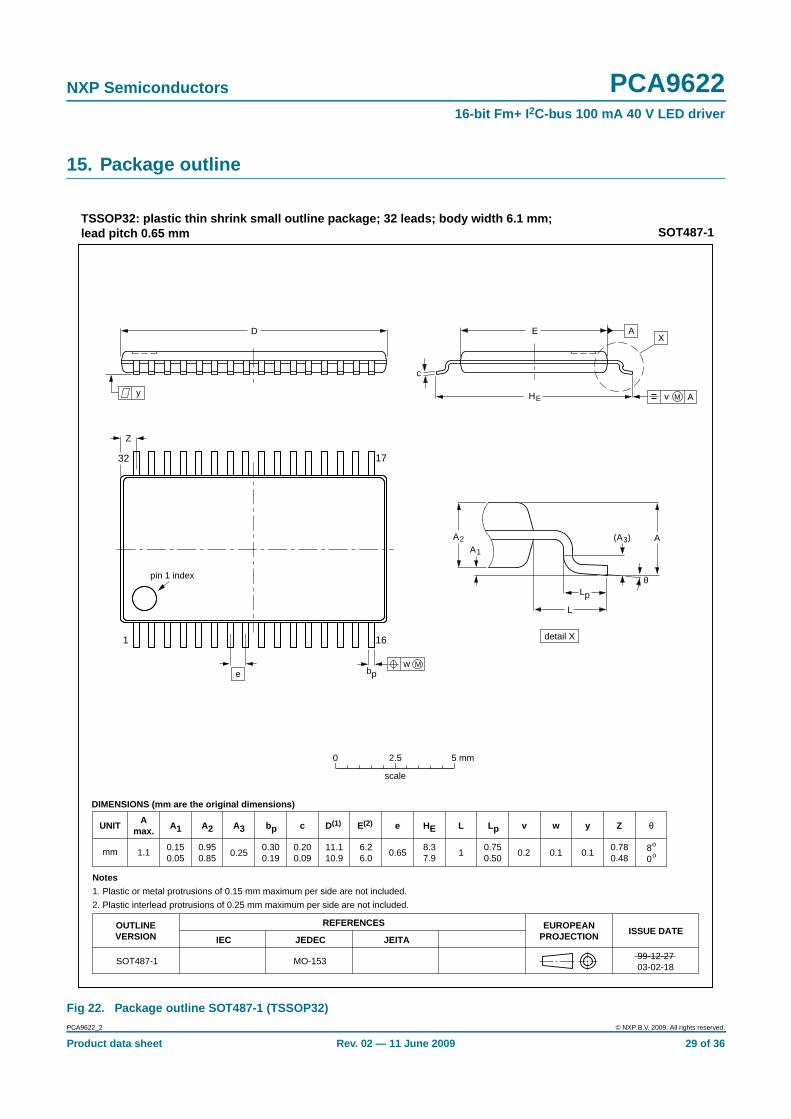
15. Package outline
Fig 22. Package outline SOT487-1 (TSSOP32)
UNIT A1 A2 A3 bp c D(1) E(2) e HE L Lp Zywv θ
REFERENCESOUTLINEVERSION
EUROPEANPROJECTION ISSUE DATE
IEC JEDEC JEITA
mm 0.150.05
0.950.85
0.300.19
0.200.09
11.110.9
6.26.0
0.658.37.9
0.780.48
80
o
o0.1 0.10.21
DIMENSIONS (mm are the original dimensions)
Notes
1. Plastic or metal protrusions of 0.15 mm maximum per side are not included.
2. Plastic interlead protrusions of 0.25 mm maximum per side are not included.
0.750.50
SOT487-1 MO-153 99-12-2703-02-18
w Mbp
D
Z
e
0.25
1 16
32 17
θ
AA1
A2
Lp
detail X
L
(A )3
HE
E
c
v M A
XA
y
0 2.5 5 mm
scale
TSSOP32: plastic thin shrink small outline package; 32 leads; body width 6.1 mm;lead pitch 0.65 mm SOT487-1
Amax.
1.1
pin 1 index
PCA9622_2 © NXP B.V. 2009. All rights reserved.
Product data sheet Rev. 02 — 11 June 2009 29 of 36

NXP Semiconductors PCA962216-bit Fm+ I 2C-bus 100 mA 40 V LED driver
Fig 23. Package outline SOT617-1 (HVQFN32)
0.51
A1 EhbUNIT ye
0.2
c
REFERENCESOUTLINEVERSION
EUROPEANPROJECTION ISSUE DATE
IEC JEDEC JEITA
mm 5.14.9
Dh
3.252.95
y1
5.14.9
3.252.95
e1
3.5
e2
3.50.300.18
0.050.00
0.05 0.1
DIMENSIONS (mm are the original dimensions)
SOT617-1 MO-220- - - - - -
0.50.3
L
0.1
v
0.05
w
0 2.5 5 mm
scale
SOT617-1HVQFN32: plastic thermal enhanced very thin quad flat package; no leads;32 terminals; body 5 x 5 x 0.85 mm
A(1)
max.
AA1
c
detail X
yy1 Ce
L
Eh
Dh
e
e1
b
9 16
32 25
24
178
1
X
D
E
C
B A
e2
terminal 1index area
terminal 1index area
01-08-0802-10-18
1/2 e
1/2 e ACC
Bv M
w M
E(1)
Note
1. Plastic or metal protrusions of 0.075 mm maximum per side are not included.
D(1)
PCA9622_2 © NXP B.V. 2009. All rights reserved.
Product data sheet Rev. 02 — 11 June 2009 30 of 36
NXP Semiconductors PCA962216-bit Fm+ I 2C-bus 100 mA 40 V LED driver
16. Handling information
All input and output pins are protected against ElectroStatic Discharge (ESD) undernormal handling. When handling ensure that the appropriate precautions are taken asdescribed in JESD625-A or equivalent standards.
17. Soldering of SMD packages
This text provides a very brief insight into a complex technology. A more in-depth accountof soldering ICs can be found in Application Note AN10365 “Surface mount reflowsoldering description”.
17.1 Introduction to solderingSoldering is one of the most common methods through which packages are attached toPrinted Circuit Boards (PCBs), to form electrical circuits. The soldered joint provides boththe mechanical and the electrical connection. There is no single soldering method that isideal for all IC packages. Wave soldering is often preferred when through-hole andSurface Mount Devices (SMDs) are mixed on one printed wiring board; however, it is notsuitable for fine pitch SMDs. Reflow soldering is ideal for the small pitches and highdensities that come with increased miniaturization.
17.2 Wave and reflow solderingWave soldering is a joining technology in which the joints are made by solder coming froma standing wave of liquid solder. The wave soldering process is suitable for the following:
• Through-hole components
• Leaded or leadless SMDs, which are glued to the surface of the printed circuit board
Not all SMDs can be wave soldered. Packages with solder balls, and some leadlesspackages which have solder lands underneath the body, cannot be wave soldered. Also,leaded SMDs with leads having a pitch smaller than ~0.6 mm cannot be wave soldered,due to an increased probability of bridging.
The reflow soldering process involves applying solder paste to a board, followed bycomponent placement and exposure to a temperature profile. Leaded packages,packages with solder balls, and leadless packages are all reflow solderable.
Key characteristics in both wave and reflow soldering are:
• Board specifications, including the board finish, solder masks and vias
• Package footprints, including solder thieves and orientation
• The moisture sensitivity level of the packages
• Package placement
• Inspection and repair
• Lead-free soldering versus SnPb soldering
17.3 Wave solderingKey characteristics in wave soldering are:
PCA9622_2 © NXP B.V. 2009. All rights reserved.
Product data sheet Rev. 02 — 11 June 2009 31 of 36
NXP Semiconductors PCA962216-bit Fm+ I 2C-bus 100 mA 40 V LED driver
• Process issues, such as application of adhesive and flux, clinching of leads, boardtransport, the solder wave parameters, and the time during which components areexposed to the wave
• Solder bath specifications, including temperature and impurities
17.4 Reflow solderingKey characteristics in reflow soldering are:
• Lead-free versus SnPb soldering; note that a lead-free reflow process usually leads tohigher minimum peak temperatures (see Figure 24) than a SnPb process, thusreducing the process window
• Solder paste printing issues including smearing, release, and adjusting the processwindow for a mix of large and small components on one board
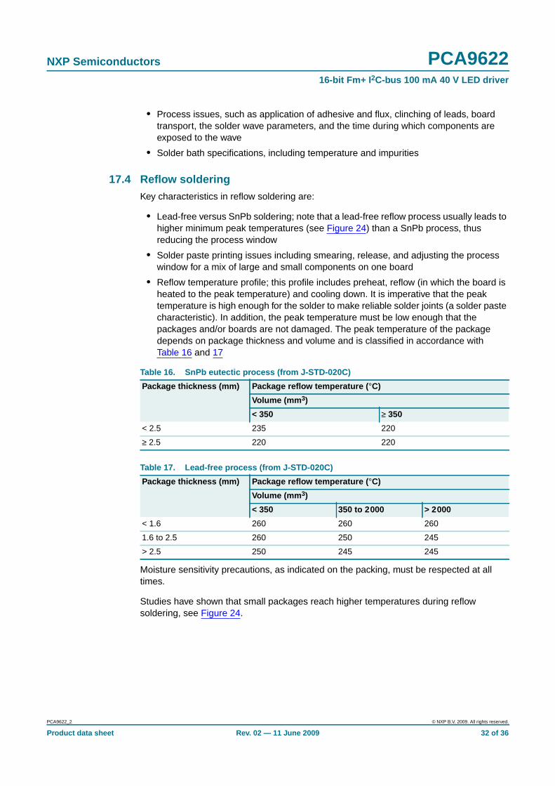
• Reflow temperature profile; this profile includes preheat, reflow (in which the board isheated to the peak temperature) and cooling down. It is imperative that the peaktemperature is high enough for the solder to make reliable solder joints (a solder pastecharacteristic). In addition, the peak temperature must be low enough that thepackages and/or boards are not damaged. The peak temperature of the packagedepends on package thickness and volume and is classified in accordance withTable 16 and 17
Moisture sensitivity precautions, as indicated on the packing, must be respected at alltimes.
Studies have shown that small packages reach higher temperatures during reflowsoldering, see Figure 24.
Table 16. SnPb eutectic process (from J-STD-020C)
Package thickness (mm) Package reflow temperature ( °C)
Volume (mm 3)
< 350 ≥ 350
< 2.5 235 220
≥ 2.5 220 220
Table 17. Lead-free process (from J-STD-020C)
Package thickness (mm) Package reflow temperature ( °C)
Volume (mm 3)
< 350 350 to 2000 > 2000
< 1.6 260 260 260
1.6 to 2.5 260 250 245
> 2.5 250 245 245
PCA9622_2 © NXP B.V. 2009. All rights reserved.
Product data sheet Rev. 02 — 11 June 2009 32 of 36

NXP Semiconductors PCA962216-bit Fm+ I 2C-bus 100 mA 40 V LED driver
For further information on temperature profiles, refer to Application Note AN10365“Surface mount reflow soldering description”.
18. Abbreviations
MSL: Moisture Sensitivity Level
Fig 24. Temperature profiles for large and small components
001aac844
temperature
time
minimum peak temperature= minimum soldering temperature
maximum peak temperature= MSL limit, damage level
peak temperature
Table 18. Abbreviations
Acronym Description
CDM Charged-Device Model
DUT Device Under Test
ESD ElectroStatic Discharge
FET Field-Effect Transistor
HBM Human Body Model
I2C-bus Inter-Integrated Circuit bus
LED Light Emitting Diode
LCD Liquid Crystal Display
LSB Least Significant Bit
MM Machine Model
MSB Most Significant Bit
NMOS Negative-channel Metal-Oxide Semiconductor
PCB Printed-Circuit Board
PMOS Positive-channel Metal-Oxide Semiconductor
PWM Pulse Width Modulation
RGB Red/Green/Blue
RGBA Red/Green/Blue/Amber
SMBus System Management Bus
PCA9622_2 © NXP B.V. 2009. All rights reserved.
Product data sheet Rev. 02 — 11 June 2009 33 of 36

NXP Semiconductors PCA962216-bit Fm+ I 2C-bus 100 mA 40 V LED driver
19. Revision history
Table 19. Revision history
Document ID Release date Data sheet status Change notice Supersedes
PCA9622_2 20090611 Product data sheet - PCA9622_1
Modifications: • Table 14 “Static characteristics”, IDD, supply current:
– Condition changed from “VDD = 2.3 V” to “VDD = 2.7 V”
– Under (new) condition VDD = 2.7 V, maximum value changed from “2 mA” to “4 mA”
– Condition changed from “VDD = 3.3 V” to “VDD = 3.6 V”
– Under (new) condition VDD = 3.6 V, maximum value changed from “5 mA” to “6 mA”
– Under condition VDD = 5.5 V, maximum value changed from “10 mA” to “12 mA”
• Table 14 “Static characteristics”, Istb, standby current:
– Condition changed from “VDD = 2.3 V” to “VDD = 2.7 V”
– Condition changed from “VDD = 3.3 V” to “VDD = 3.6 V”
• Table 14 “Static characteristics”, sub-section “OE input”:
– Ci, input capacitance typical value changed from “3.7 pF” to “15 pF”
– Ci, input capacitance maximum value changed from “5 pF” to “40 pF”
PCA9622_1 20090327 Product data sheet - -
PCA9622_2 © NXP B.V. 2009. All rights reserved.
Product data sheet Rev. 02 — 11 June 2009 34 of 36

NXP Semiconductors PCA962216-bit Fm+ I 2C-bus 100 mA 40 V LED driver
20. Legal information
20.1 Data sheet status
[1] Please consult the most recently issued document before initiating or completing a design.
[2] The term ‘short data sheet’ is explained in section “Definitions”.
[3] The product status of device(s) described in this document may have changed since this document was published and may differ in case of multiple devices. The latest product statusinformation is available on the Internet at URL http://www.nxp.com.
20.2 Definitions
Draft — The document is a draft version only. The content is still underinternal review and subject to formal approval, which may result inmodifications or additions. NXP Semiconductors does not give anyrepresentations or warranties as to the accuracy or completeness ofinformation included herein and shall have no liability for the consequences ofuse of such information.
Short data sheet — A short data sheet is an extract from a full data sheetwith the same product type number(s) and title. A short data sheet is intendedfor quick reference only and should not be relied upon to contain detailed andfull information. For detailed and full information see the relevant full datasheet, which is available on request via the local NXP Semiconductors salesoffice. In case of any inconsistency or conflict with the short data sheet, thefull data sheet shall prevail.
20.3 Disclaimers
General — Information in this document is believed to be accurate andreliable. However, NXP Semiconductors does not give any representations orwarranties, expressed or implied, as to the accuracy or completeness of suchinformation and shall have no liability for the consequences of use of suchinformation.
Right to make changes — NXP Semiconductors reserves the right to makechanges to information published in this document, including withoutlimitation specifications and product descriptions, at any time and withoutnotice. This document supersedes and replaces all information supplied priorto the publication hereof.
Suitability for use — NXP Semiconductors products are not designed,authorized or warranted to be suitable for use in medical, military, aircraft,space or life support equipment, nor in applications where failure ormalfunction of an NXP Semiconductors product can reasonably be expectedto result in personal injury, death or severe property or environmental
damage. NXP Semiconductors accepts no liability for inclusion and/or use ofNXP Semiconductors products in such equipment or applications andtherefore such inclusion and/or use is at the customer’s own risk.
Applications — Applications that are described herein for any of theseproducts are for illustrative purposes only. NXP Semiconductors makes norepresentation or warranty that such applications will be suitable for thespecified use without further testing or modification.
Limiting values — Stress above one or more limiting values (as defined inthe Absolute Maximum Ratings System of IEC 60134) may cause permanentdamage to the device. Limiting values are stress ratings only and operation ofthe device at these or any other conditions above those given in theCharacteristics sections of this document is not implied. Exposure to limitingvalues for extended periods may affect device reliability.
Terms and conditions of sale — NXP Semiconductors products are soldsubject to the general terms and conditions of commercial sale, as publishedat http://www.nxp.com/profile/terms, including those pertaining to warranty,intellectual property rights infringement and limitation of liability, unlessexplicitly otherwise agreed to in writing by NXP Semiconductors. In case ofany inconsistency or conflict between information in this document and suchterms and conditions, the latter will prevail.
No offer to sell or license — Nothing in this document may be interpretedor construed as an offer to sell products that is open for acceptance or thegrant, conveyance or implication of any license under any copyrights, patentsor other industrial or intellectual property rights.
Export control — This document as well as the item(s) described hereinmay be subject to export control regulations. Export might require a priorauthorization from national authorities.
20.4 TrademarksNotice: All referenced brands, product names, service names and trademarksare the property of their respective owners.
I2C-bus — logo is a trademark of NXP B.V.
21. Contact information
For more information, please visit: http://www .nxp.com
For sales office addresses, please send an email to: salesad [email protected]
Document status [1] [2] Product status [3] Definition
Objective [short] data sheet Development This document contains data from the objective specification for product development.
Preliminary [short] data sheet Qualification This document contains data from the preliminary specification.
Product [short] data sheet Production This document contains the product specification.
PCA9622_2 © NXP B.V. 2009. All rights reserved.
Product data sheet Rev. 02 — 11 June 2009 35 of 36
NXP Semiconductors PCA962216-bit Fm+ I 2C-bus 100 mA 40 V LED driver
22. Contents
1 General description . . . . . . . . . . . . . . . . . . . . . . 12 Features . . . . . . . . . . . . . . . . . . . . . . . . . . . . . . . 23 Applications . . . . . . . . . . . . . . . . . . . . . . . . . . . . 34 Ordering information . . . . . . . . . . . . . . . . . . . . . 35 Block diagram . . . . . . . . . . . . . . . . . . . . . . . . . . 46 Pinning information . . . . . . . . . . . . . . . . . . . . . . 56.1 Pinning . . . . . . . . . . . . . . . . . . . . . . . . . . . . . . . 56.2 Pin description . . . . . . . . . . . . . . . . . . . . . . . . . 57 Functional description . . . . . . . . . . . . . . . . . . . 77.1 Device addresses . . . . . . . . . . . . . . . . . . . . . . . 77.1.1 Regular I2C-bus slave address . . . . . . . . . . . . . 77.1.2 LED All Call I2C-bus address . . . . . . . . . . . . . . 87.1.3 LED Sub Call I2C-bus addresses . . . . . . . . . . . 87.1.4 Software Reset I2C-bus address . . . . . . . . . . . 87.2 Control register . . . . . . . . . . . . . . . . . . . . . . . . . 97.3 Register definitions . . . . . . . . . . . . . . . . . . . . . 107.3.1 Mode register 1, MODE1 . . . . . . . . . . . . . . . . 117.3.2 Mode register 2, MODE2 . . . . . . . . . . . . . . . . 127.3.3 PWM0 to PWM15, individual brightness
control . . . . . . . . . . . . . . . . . . . . . . . . . . . . . . . 127.3.4 GRPPWM, group duty cycle control . . . . . . . . 137.3.5 GRPFREQ, group frequency . . . . . . . . . . . . . 137.3.6 LEDOUT0 to LEDOUT3, LED driver
output state . . . . . . . . . . . . . . . . . . . . . . . . . . . 147.3.7 SUBADR1 to SUBADR3, I2C-bus
subaddress 1 to 3 . . . . . . . . . . . . . . . . . . . . . . 147.3.8 ALLCALLADR, LED All Call
I2C-bus address . . . . . . . . . . . . . . . . . . . . . . . 157.4 Active LOW output enable input . . . . . . . . . . . 157.5 Power-on reset . . . . . . . . . . . . . . . . . . . . . . . . 167.6 Software reset. . . . . . . . . . . . . . . . . . . . . . . . . 167.7 Individual brightness control with group
dimming/blinking . . . . . . . . . . . . . . . . . . . . . . . 178 Characteristics of the I 2C-bus. . . . . . . . . . . . . 188.1 Bit transfer . . . . . . . . . . . . . . . . . . . . . . . . . . . 188.1.1 START and STOP conditions . . . . . . . . . . . . . 188.2 System configuration . . . . . . . . . . . . . . . . . . . 188.3 Acknowledge . . . . . . . . . . . . . . . . . . . . . . . . . 199 Bus transactions . . . . . . . . . . . . . . . . . . . . . . . 2010 Application design-in information . . . . . . . . . 2211 Limiting values. . . . . . . . . . . . . . . . . . . . . . . . . 2312 Static characteristics. . . . . . . . . . . . . . . . . . . . 2413 Dynamic characteristics . . . . . . . . . . . . . . . . . 2614 Test information . . . . . . . . . . . . . . . . . . . . . . . . 2815 Package outline . . . . . . . . . . . . . . . . . . . . . . . . 29
16 Handling information . . . . . . . . . . . . . . . . . . . 3117 Soldering of SMD packages . . . . . . . . . . . . . . 3117.1 Introduction to soldering. . . . . . . . . . . . . . . . . 3117.2 Wave and reflow soldering . . . . . . . . . . . . . . . 3117.3 Wave soldering. . . . . . . . . . . . . . . . . . . . . . . . 3117.4 Reflow soldering. . . . . . . . . . . . . . . . . . . . . . . 3218 Abbreviations . . . . . . . . . . . . . . . . . . . . . . . . . 3319 Revision history . . . . . . . . . . . . . . . . . . . . . . . 3420 Legal information . . . . . . . . . . . . . . . . . . . . . . 3520.1 Data sheet status . . . . . . . . . . . . . . . . . . . . . . 3520.2 Definitions . . . . . . . . . . . . . . . . . . . . . . . . . . . 3520.3 Disclaimers. . . . . . . . . . . . . . . . . . . . . . . . . . . 3520.4 Trademarks . . . . . . . . . . . . . . . . . . . . . . . . . . 3521 Contact information . . . . . . . . . . . . . . . . . . . . 3522 Contents. . . . . . . . . . . . . . . . . . . . . . . . . . . . . . 36
© NXP B.V. 2009. All rights reserved.For more information, please visit: http://www.nxp.comFor sales office addresses, please send an email to: [email protected]
Date of release: 11 June 2009
Document identifier: PCA9622_2
Please be aware that important notices concerning this document and the product(s)described herein, have been included in section ‘Legal information’.


![Home - Denver Philharmonicdenverphilharmonic.org/wp-content/uploads/2018/05/...SHOSTAKOVICH Symphony No. 5, Movement II Contra Bassoon [] XXX] [XXXXXXXXXXXXXXXXXXXXXX XXXXXXXXXXXXX](https://img.pdfslide.us/doc/110x75/6101bb9fb679f8228619829f/home-denver-philharmon-shostakovich-symphony-no-5-movement-ii-contra-bassoon.jpg)
![ProLight PBVC-10FWU-F3G 10W Power LED Version: 1EV External Visual JESD22 B-101 N/A See notes [2] 0 HTFB High Temperature Forward Bias JESD22-A108 Tamb =85 C, IF = max. DC [1] 1000](https://img.pdfslide.us/doc/110x75/6127a9601ad5444e340186c0/prolight-pbvc-10fwu-f3g-10w-power-led-version-1-ev-external-visual-jesd22-b-101.jpg)