Embed Size (px)
Citation preview
PCA8565Real time clock/calenderRev. 01 — 31 March 2003 Product data
1. General description
The PCA8565 is a CMOS real time clock/calendar optimized for low powerconsumption. A programmable clock output, interrupt output and voltage-low detectorare also provided. All address and data are transferred serially via a two-linebidirectional I2C-bus. Maximum bus speed is 400 kbit/s. The built-in word addressregister is incremented automatically after each written or read data byte.
2. Features
Provides year, month, day, weekday, hours, minutes and seconds based on32.768 kHz quartz crystal
Century flag
Clock operating voltage: 1.8 to 5.5 V
Extended operating temperature range: −40 to +125 °C Low backup current; typical 0.5 µA at VDD = 3.0 V and Tamb = 25 °C 400 kHz two-wire I2C-bus interface (at VDD = 1.8 to 5.5 V)
Programmable clock output for peripheral devices (32.768 kHz, 1024 Hz,32 Hz and 1 Hz)
Alarm and timer functions
Integrated oscillator capacitor
Internal power-on reset
I2C-bus slave address: read A3H and write A2H
Open-drain interrupt pin.
3. Applications
Automotive
Industrial
Other applications that require a wide operating temperature range.
4. Quick reference data
Table 1: Quick reference data
Symbol Parameter Conditions Min Typ Max Unit
VDD supply voltage I2C-bus active; fSCL = 400 kHz;Tamb = −40 to +125 °C
1.8 - 5.5 V
IDD supply current fSCL = 400 kHz - - 820 µA
Tamb ambient temperature −40 - +125 °C
Philips Semiconductors PCA8565Real time clock/calender
5. Ordering information
6. Block diagram
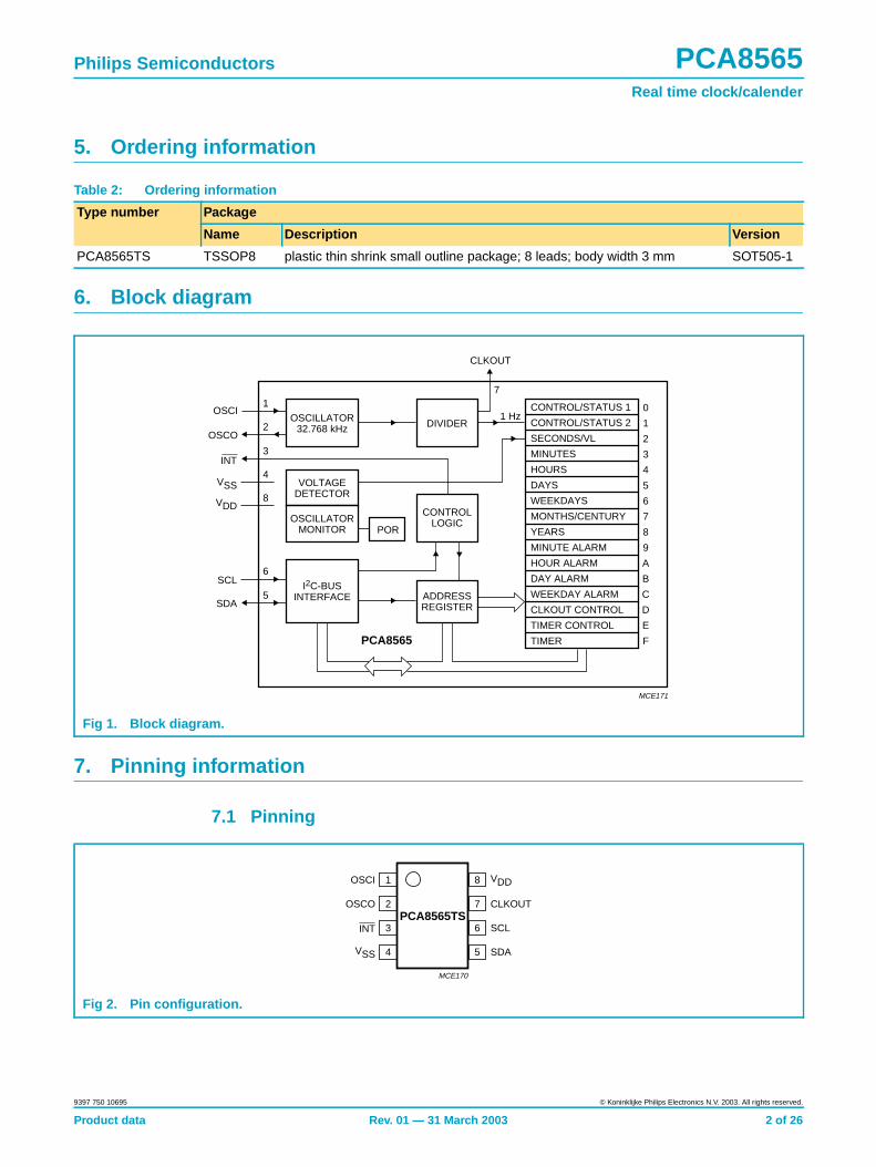
7. Pinning information
7.1 Pinning
Table 2: Ordering information
Type number Package
Name Description Version
PCA8565TS TSSOP8 plastic thin shrink small outline package; 8 leads; body width 3 mm SOT505-1
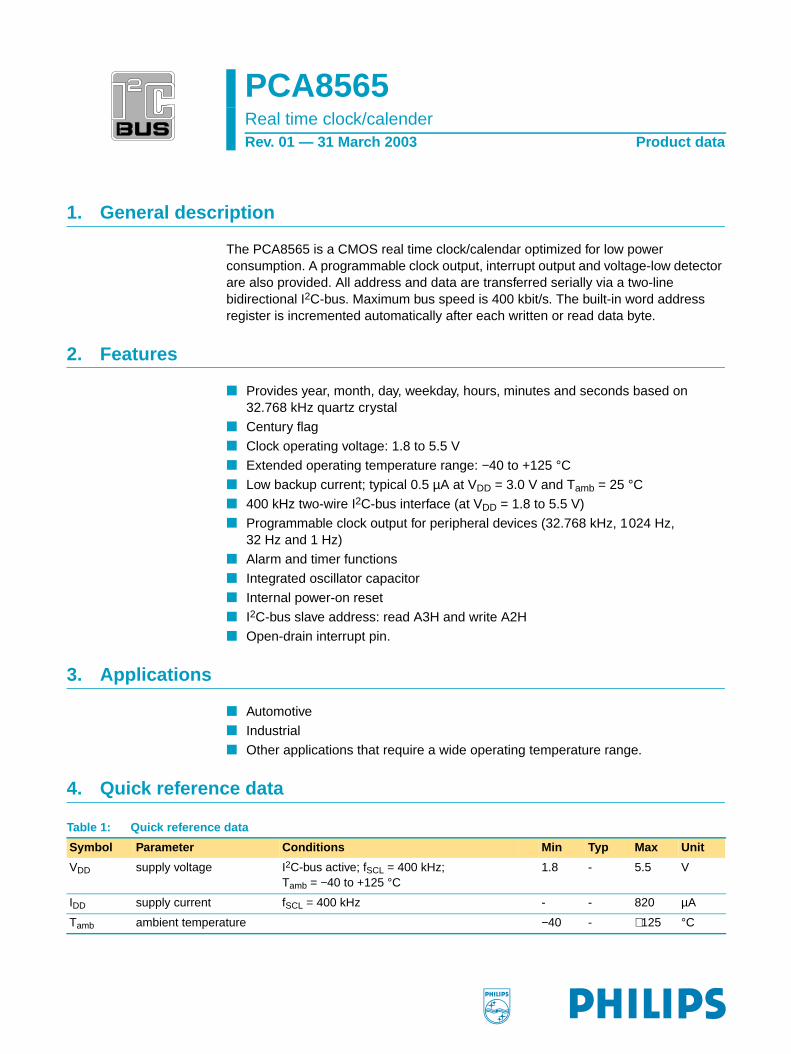
Fig 1. Block diagram.
MCE171
0CONTROL/STATUS 1OSCILLATOR
32.768 kHz 1CONTROL/STATUS 2
2SECONDS/VL
3MINUTES
4HOURS
5DAYS
6WEEKDAYS
7MONTHS/CENTURY
8YEARS
9MINUTE ALARM
AHOUR ALARM
BDAY ALARM
CWEEKDAY ALARM
D
E
CLKOUT CONTROL
F
TIMER CONTROL
TIMER
OSCILLATORMONITOR
VOLTAGEDETECTOR
I2C-BUSINTERFACE
DIVIDER
PCA8565
CONTROLLOGIC
ADDRESSREGISTER
POR
VDD
CLKOUT
1 Hz
OSCO
SCL
SDA
VSS
INT
OSCI1
2
3
4
8
6
5
7
Fig 2. Pin configuration.
MCE170
PCA8565TS
1
2
3
4
OSCI
OSCO
INT
VSS
VDD
CLKOUT
SCL
SDA
8
7
6
5
Product data Rev. 01 — 31 March 2003 2 of 26
9397 750 10695 © Koninklijke Philips Electronics N.V. 2003. All rights reserved.
Philips Semiconductors PCA8565Real time clock/calender
7.2 Pin description
8. Functional description
The PCA8565 contains sixteen 8-bit registers with an auto-incrementing addressregister, an on-chip 32.768 kHz oscillator with one integrated capacitor, a frequencydivider which provides the source clock for the Real Time Clock/calender (RTC), aprogrammable clock output, a timer, an alarm, a voltage-low detector and a 400 kHzI2C-bus interface.
All 16 registers are designed as addressable 8-bit parallel registers although not allbits are implemented. The first two registers (memory address 00H and 01H) areused as control and/or status registers. The memory addresses 02H through 08H areused as counters for the clock function (seconds up to years counters). Addresslocations 09H through 0CH contain alarm registers which define the conditions for analarm. Address 0DH controls the CLKOUT output frequency. 0EH and 0FH are thetimer control and timer registers, respectively.
The seconds, minutes, hours, days, weekdays, months, years as well as the minutealarm, hour alarm, day alarm and weekday alarm registers are all coded in BCDformat.
When one of the RTC registers is read the contents of all counters are frozen.Therefore, faulty reading of the clock/calendar during a carry condition is prevented.
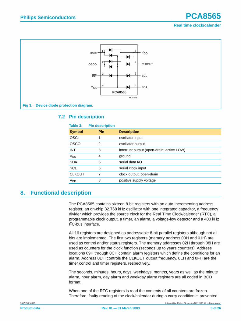
Fig 3. Device diode protection diagram.
MCE169
SDA4 5
VSS
SCL3 6
INT
CLKOUT2 7
OSCO
VDD1 8
OSCI
PCA8565
Table 3: Pin description
Symbol Pin Description
OSCI 1 oscillator input
OSCO 2 oscillator output
INT 3 interrupt output (open-drain; active LOW)
VSS 4 ground
SDA 5 serial data I/O
SCL 6 serial clock input
CLKOUT 7 clock output, open-drain
VDD 8 positive supply voltage
Product data Rev. 01 — 31 March 2003 3 of 26
9397 750 10695 © Koninklijke Philips Electronics N.V. 2003. All rights reserved.
Philips Semiconductors PCA8565Real time clock/calender
8.1 Alarm function modesBy clearing the MSB of one or more of the alarm registers (bit AE = alarm enable),the corresponding alarm condition(s) will be active. In this way an alarm can begenerated from once per minute up to once per week. The alarm condition sets theAlarm Flag (AF). The asserted AF can be used to generate an interrupt (INT).The AF can only be cleared by software.
8.2 TimerThe 8-bit countdown timer at address 0FH is controlled by the timer control register ataddress 0EH. The timer control register determines one of 4 source clockfrequencies for the timer (4096 Hz, 64 Hz, 1 Hz, or 1⁄60 Hz), and enables or disablesthe timer. The timer counts down from a software-loaded 8-bit binary value. At theend of every countdown, the timer sets the Timer Flag (TF). The TF may only becleared by software. The asserted TF can be used to generate an Interrupt (INT). Theinterrupt may be generated as a pulsed signal every countdown period or as apermanently active signal which follows the condition of TF. Bit TI/TP is used tocontrol this mode selection. When reading the timer, the current countdown value isreturned.
8.3 CLKOUT outputA programmable square wave is available at pin CLKOUT. Operation is controlled bythe CLKOUT control register at address 0DH. Frequencies of 32.768 kHz (default),1024 Hz, 32 Hz and 1 Hz can be generated for use as a system clock,microcontroller clock, input to a charge pump, or for calibration of the oscillator.CLKOUT is an open-drain output and enabled at power-on. If disabled it becomeshigh-impedance.
8.4 ResetThe PCA8565 includes an internal reset circuit which is active whenever the oscillatoris stopped. In the reset state the I2C-bus logic is initialized and all registers, includingthe address pointer, are cleared with the exception of bits FE, VL, TD1, TD0, TESTCand AE which are set to logic 1.
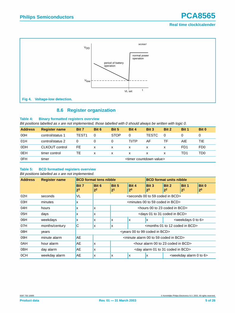
8.5 Voltage-low detectorThe PCA8565 has an on-chip voltage-low detector. When VDD drops below Vlow,bit VL in the seconds register is set to indicate that the integrity of the clockinformation is no longer guaranteed. The VL flag can only be cleared by software.
Bit VL is intended to detect the situation when VDD is decreasing slowly, for exampleunder battery operation. Should VDD reach Vlow before power is re-asserted thenbit VL will be set. This will indicate that the time may be corrupted.
Product data Rev. 01 — 31 March 2003 4 of 26
9397 750 10695 © Koninklijke Philips Electronics N.V. 2003. All rights reserved.
Philips Semiconductors PCA8565Real time clock/calender
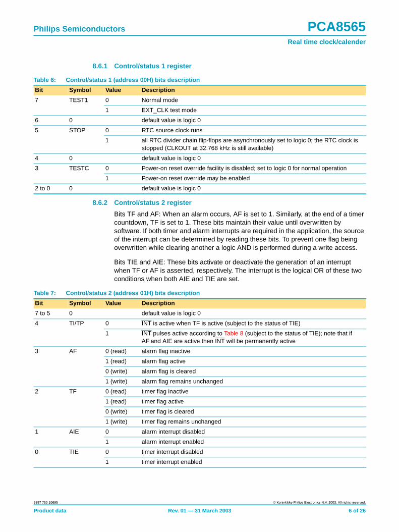
8.6 Register organization
Fig 4. Voltage-low detection.
handbook, halfpage
VL set
normal poweroperation
period of batteryoperation
t
VDD
Vlow
MGR887
Table 4: Binary formatted registers overviewBit positions labelled as x are not implemented, those labelled with 0 should always be written with logic 0.
Address Register name Bit 7 Bit 6 Bit 5 Bit 4 Bit 3 Bit 2 Bit 1 Bit 0
00H control/status 1 TEST1 0 STOP 0 TESTC 0 0 0
01H control/status 2 0 0 0 TI/TP AF TF AIE TIE
0DH CLKOUT control FE x x x x x FD1 FD0
0EH timer control TE x x x x x TD1 TD0
0FH timer <timer countdown value>
Table 5: BCD formatted registers overviewBit positions labelled as x are not implemented.
Address Register name BCD format tens nibble BCD format units nibble
Bit 723
Bit 622
Bit 521
Bit 420
Bit 323
Bit 222
Bit 121
Bit 020
02H seconds VL <seconds 00 to 59 coded in BCD>
03H minutes x <minutes 00 to 59 coded in BCD>
04H hours x x <hours 00 to 23 coded in BCD>
05H days x x <days 01 to 31 coded in BCD>
06H weekdays x x x x x <weekdays 0 to 6>
07H months/century C x x <months 01 to 12 coded in BCD>
08H years <years 00 to 99 coded in BCD>
09H minute alarm AE <minute alarm 00 to 59 coded in BCD>
0AH hour alarm AE x <hour alarm 00 to 23 coded in BCD>
0BH day alarm AE x <day alarm 01 to 31 coded in BCD>
0CH weekday alarm AE x x x x <weekday alarm 0 to 6>
Product data Rev. 01 — 31 March 2003 5 of 26
9397 750 10695 © Koninklijke Philips Electronics N.V. 2003. All rights reserved.
Philips Semiconductors PCA8565Real time clock/calender
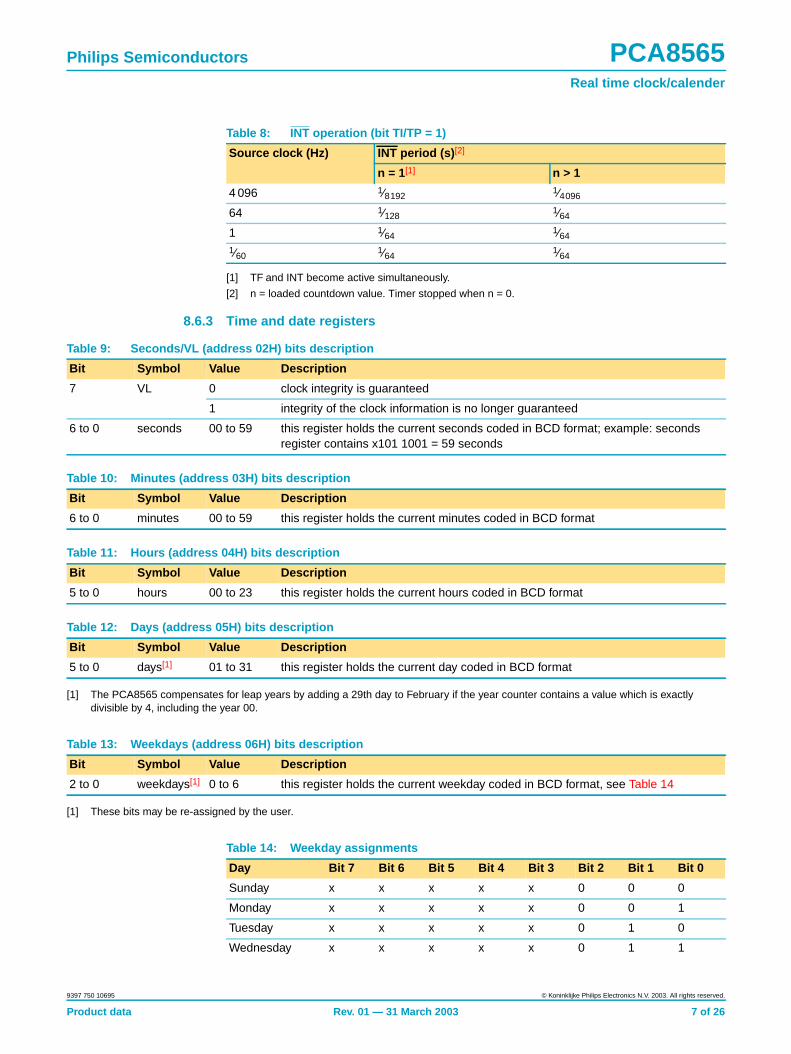
8.6.1 Control/status 1 register
8.6.2 Control/status 2 register
Bits TF and AF: When an alarm occurs, AF is set to 1. Similarly, at the end of a timercountdown, TF is set to 1. These bits maintain their value until overwritten bysoftware. If both timer and alarm interrupts are required in the application, the sourceof the interrupt can be determined by reading these bits. To prevent one flag beingoverwritten while clearing another a logic AND is performed during a write access.
Bits TIE and AIE: These bits activate or deactivate the generation of an interruptwhen TF or AF is asserted, respectively. The interrupt is the logical OR of these twoconditions when both AIE and TIE are set.
Table 6: Control/status 1 (address 00H) bits description
Bit Symbol Value Description
7 TEST1 0 Normal mode
1 EXT_CLK test mode
6 0 default value is logic 0
5 STOP 0 RTC source clock runs
1 all RTC divider chain flip-flops are asynchronously set to logic 0; the RTC clock isstopped (CLKOUT at 32.768 kHz is still available)
4 0 default value is logic 0
3 TESTC 0 Power-on reset override facility is disabled; set to logic 0 for normal operation
1 Power-on reset override may be enabled
2 to 0 0 default value is logic 0
Table 7: Control/status 2 (address 01H) bits description
Bit Symbol Value Description
7 to 5 0 default value is logic 0
4 TI/TP 0 INT is active when TF is active (subject to the status of TIE)
1 INT pulses active according to Table 8 (subject to the status of TIE); note that ifAF and AIE are active then INT will be permanently active
3 AF 0 (read) alarm flag inactive
1 (read) alarm flag active
0 (write) alarm flag is cleared
1 (write) alarm flag remains unchanged
2 TF 0 (read) timer flag inactive
1 (read) timer flag active
0 (write) timer flag is cleared
1 (write) timer flag remains unchanged
1 AIE 0 alarm interrupt disabled
1 alarm interrupt enabled
0 TIE 0 timer interrupt disabled
1 timer interrupt enabled
Product data Rev. 01 — 31 March 2003 6 of 26
9397 750 10695 © Koninklijke Philips Electronics N.V. 2003. All rights reserved.
Philips Semiconductors PCA8565Real time clock/calender
[1] TF and INT become active simultaneously.
[2] n = loaded countdown value. Timer stopped when n = 0.
8.6.3 Time and date registers
[1] The PCA8565 compensates for leap years by adding a 29th day to February if the year counter contains a value which is exactlydivisible by 4, including the year 00.
[1] These bits may be re-assigned by the user.
Table 8: INT operation (bit TI/TP = 1)
Source clock (Hz) INT period (s) [2]
n = 1[1] n > 1
4 096 1⁄81921⁄4096
64 1⁄1281⁄64
1 1⁄641⁄64
1⁄601⁄64
1⁄64
Table 9: Seconds/VL (address 02H) bits description
Bit Symbol Value Description
7 VL 0 clock integrity is guaranteed
1 integrity of the clock information is no longer guaranteed
6 to 0 seconds 00 to 59 this register holds the current seconds coded in BCD format; example: secondsregister contains x101 1001 = 59 seconds
Table 10: Minutes (address 03H) bits description
Bit Symbol Value Description
6 to 0 minutes 00 to 59 this register holds the current minutes coded in BCD format
Table 11: Hours (address 04H) bits description
Bit Symbol Value Description
5 to 0 hours 00 to 23 this register holds the current hours coded in BCD format
Table 12: Days (address 05H) bits description
Bit Symbol Value Description
5 to 0 days[1] 01 to 31 this register holds the current day coded in BCD format
Table 13: Weekdays (address 06H) bits description
Bit Symbol Value Description
2 to 0 weekdays[1] 0 to 6 this register holds the current weekday coded in BCD format, see Table 14
Table 14: Weekday assignments
Day Bit 7 Bit 6 Bit 5 Bit 4 Bit 3 Bit 2 Bit 1 Bit 0
Sunday x x x x x 0 0 0
Monday x x x x x 0 0 1
Tuesday x x x x x 0 1 0
Wednesday x x x x x 0 1 1
Product data Rev. 01 — 31 March 2003 7 of 26
9397 750 10695 © Koninklijke Philips Electronics N.V. 2003. All rights reserved.
Philips Semiconductors PCA8565Real time clock/calender
[1] These bits may be re-assigned by the user.
8.6.4 Alarm registers
When one or more of these registers are loaded with a valid minute, hour, day orweekday and its corresponding bit Alarm Enable (AE) is logic 0, then that informationwill be compared with the current minute, hour, day and weekday. When all enabledcomparisons first match, the Alarm Flag (AF) is set. AF will remain set until clearedby software. Once AF has been cleared it will only be set again when the timeincrements to match the alarm condition once more. Alarm registers which have theirbit AE at logic 1 will be ignored.
Thursday x x x x x 1 0 0
Friday x x x x x 1 0 1
Saturday x x x x x 1 1 0
Table 14: Weekday assignments …continued
Day Bit 7 Bit 6 Bit 5 Bit 4 Bit 3 Bit 2 Bit 1 Bit 0
Table 15: Months/century (address 07H) bits description
Bit Symbol Value Description
7 century[1] this bit is toggled when the years register overflows from 99 to 00
0 indicates the century is 20xx
1 indicates the century is 19xx
4 to 0 month 01 to 12 this register holds the current month coded in BCD format, see Table 16
Table 16: Month assignments
Month Bit 7 Bit 6 Bit 5 Bit 4 Bit 3 Bit 2 Bit 1 Bit 0
January C x x 0 0 0 0 1
February C x x 0 0 0 1 0
March C x x 0 0 0 1 1
April C x x 0 0 1 0 0
May C x x 0 0 1 0 1
June C x x 0 0 1 1 0
July C x x 0 0 1 1 1
August C x x 0 1 0 0 0
September C x x 0 1 0 0 1
October C x x 1 0 0 0 0
November C x x 1 0 0 0 1
December C x x 1 0 0 1 0
Table 17: Years (address 08H) bits description
Bit Symbol Value Description
7 to 0 years 00 to 99 this register holds the current year coded in BCD format
Product data Rev. 01 — 31 March 2003 8 of 26
9397 750 10695 © Koninklijke Philips Electronics N.V. 2003. All rights reserved.
Philips Semiconductors PCA8565Real time clock/calender
8.6.5 CLOCKOUT control register
8.6.6 Countdown timer
The timer register is an 8-bit binary countdown timer. It is enabled and disabled viathe timer control register bit TE. The source clock for the timer is also selected by thetimer control register. Other timer properties such as interrupt generation arecontrolled via control/status 2 register.
Table 18: Minute alarm (address 09H) bits description
Bit Symbol Value Description
7 AE 0 minute alarm is enabled
1 minute alarm is disabled
6 to 0 alarm minutes 00 to 59 this register holds the minute alarm information coded in BCD format
Table 19: Hour alarm (address 0AH) bits description
Bit Symbol Value Description
7 AE 0 hour alarm is enabled
1 hour alarm is disabled
5 to 0 alarm hours 00 to 23 this register holds the hour alarm information coded in BCD format
Table 20: Day alarm (address 0BH) bits description
Bit Symbol Value Description
7 AE 0 day alarm is enabled
1 day alarm is disabled
5 to 0 alarm days 01 to 31 this register holds the day alarm information coded in BCD format
Table 21: Weekday alarm (address 0CH) bits description
Bit Symbol Value Description
7 AE 0 weekday alarm is enabled
1 weekday alarm is disabled
2 to 0 alarmweekdays
0 to 6 this register holds the weekday alarm information coded in BCD format
Table 22: CLKOUT control (address 0DH) bits description
Bit Symbol Value Description
7 FE 0 the CLKOUT output is inhibited and CLKOUT output is set to high-impedance
1 the CLKOUT output is activated
1 to 0 FD1 andFD0
these bits control the frequency output at pin CLKOUT, see Table 23
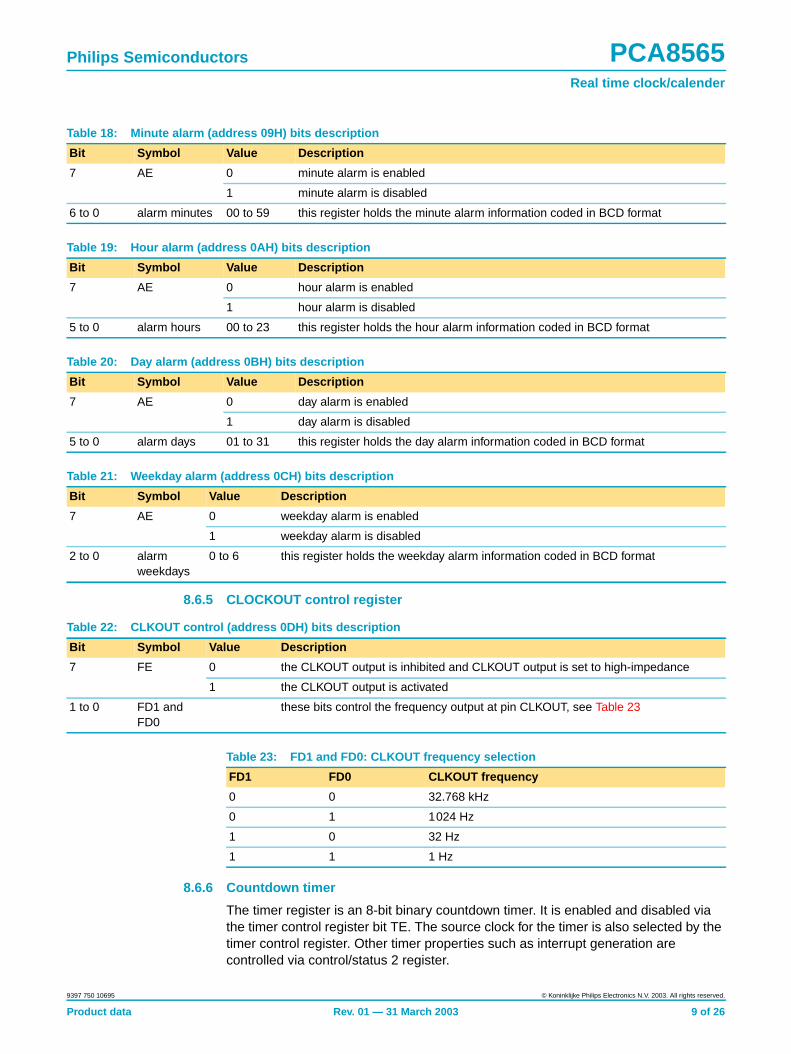
Table 23: FD1 and FD0: CLKOUT frequency selection
FD1 FD0 CLKOUT frequency
0 0 32.768 kHz
0 1 1024 Hz
1 0 32 Hz
1 1 1 Hz
Product data Rev. 01 — 31 March 2003 9 of 26
9397 750 10695 © Koninklijke Philips Electronics N.V. 2003. All rights reserved.
Philips Semiconductors PCA8565Real time clock/calender
For accurate read back of the countdown value, the I2C-bus clock (SCL) must beoperating at a frequency of at least twice the selected timer clock.
8.7 EXT_CLK test modeA test mode is available which allows for on-board testing. In such a mode it ispossible to set up test conditions and control the operation of the RTC.
The test mode is entered by setting bit TEST1 in control/status1 register. Thenpin CLKOUT becomes an input. The test mode replaces the internal 64 Hz signalwith the signal applied to pin CLKOUT. Every 64 positive edges applied topin CLKOUT will then generate an increment of one second.
The signal applied to pin CLKOUT should have a minimum pulse width of 300 ns anda minimum period of 1000 ns. The internal 64 Hz clock, now sourced from CLKOUT,is divided down to 1 Hz by a 26 divide chain called a pre-scaler. The pre-scaler can beset into a known state by using bit STOP. When bit STOP is set, the pre-scaler isreset to 0 (STOP must be cleared before the pre-scaler can operate again).
From a STOP condition, the first 1 second increment will take place after 32 positiveedges on CLKOUT. Thereafter, every 64 positive edges will cause a 1 secondincrement.
Remark: Entry into EXT_CLK test mode is not synchronized to the internal 64 Hzclock. When entering the test mode, no assumption as to the state of the pre-scalercan be made.
Operation example:
1. Set EXT_CLK test mode (control/status 1, bit TEST1 = 1)
2. Set STOP (control/status 1, bit STOP = 1)
Table 24: Timer control (address 0EH) bits description
Bit Symbol Value Description
7 TE 0 timer is disabled
1 timer is enabled
1 to 0 TD1 andTD0
timer source clock frequency select; these bits determine the source clock for thecountdown timer, see Table 25; when not in use, TD1 and TD0 should be set to1⁄16 Hz for power saving
Table 25: TD1 and TD0: Timer frequency selection
TD1 TD0 TIMER Source clock frequency
0 0 4096 Hz
0 1 64 Hz
1 0 1 Hz
1 1 1⁄60 Hz
Table 26: Timer (address 0FH) bits description
Bit Symbol Value Description
7 to 0 timer 00 to FFcountdown value = n; CountdownPeriod
nSourceClockFrequency---------------------------------------------------------------=
Product data Rev. 01 — 31 March 2003 10 of 26
9397 750 10695 © Koninklijke Philips Electronics N.V. 2003. All rights reserved.
Philips Semiconductors PCA8565Real time clock/calender
3. Clear STOP (control/status 1, bit STOP = 0)
4. Set time registers to desired value
5. Apply 32 clock pulses to CLKOUT
6. Read time registers to see the first change
7. Apply 64 clock pulses to CLKOUT
8. Read time registers to see the second change.
Repeat 7 and 8 for additional increments.
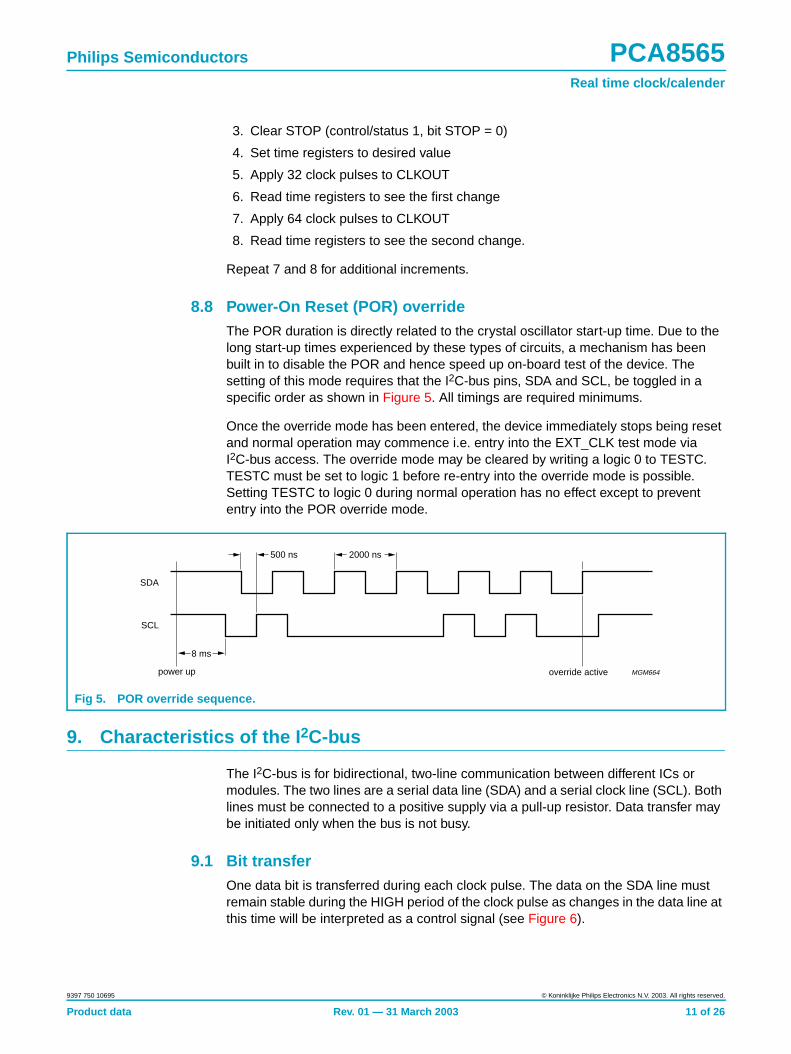
8.8 Power-On Reset (POR) overrideThe POR duration is directly related to the crystal oscillator start-up time. Due to thelong start-up times experienced by these types of circuits, a mechanism has beenbuilt in to disable the POR and hence speed up on-board test of the device. Thesetting of this mode requires that the I2C-bus pins, SDA and SCL, be toggled in aspecific order as shown in Figure 5. All timings are required minimums.
Once the override mode has been entered, the device immediately stops being resetand normal operation may commence i.e. entry into the EXT_CLK test mode viaI2C-bus access. The override mode may be cleared by writing a logic 0 to TESTC.TESTC must be set to logic 1 before re-entry into the override mode is possible.Setting TESTC to logic 0 during normal operation has no effect except to prevententry into the POR override mode.
9. Characteristics of the I 2C-bus
The I2C-bus is for bidirectional, two-line communication between different ICs ormodules. The two lines are a serial data line (SDA) and a serial clock line (SCL). Bothlines must be connected to a positive supply via a pull-up resistor. Data transfer maybe initiated only when the bus is not busy.
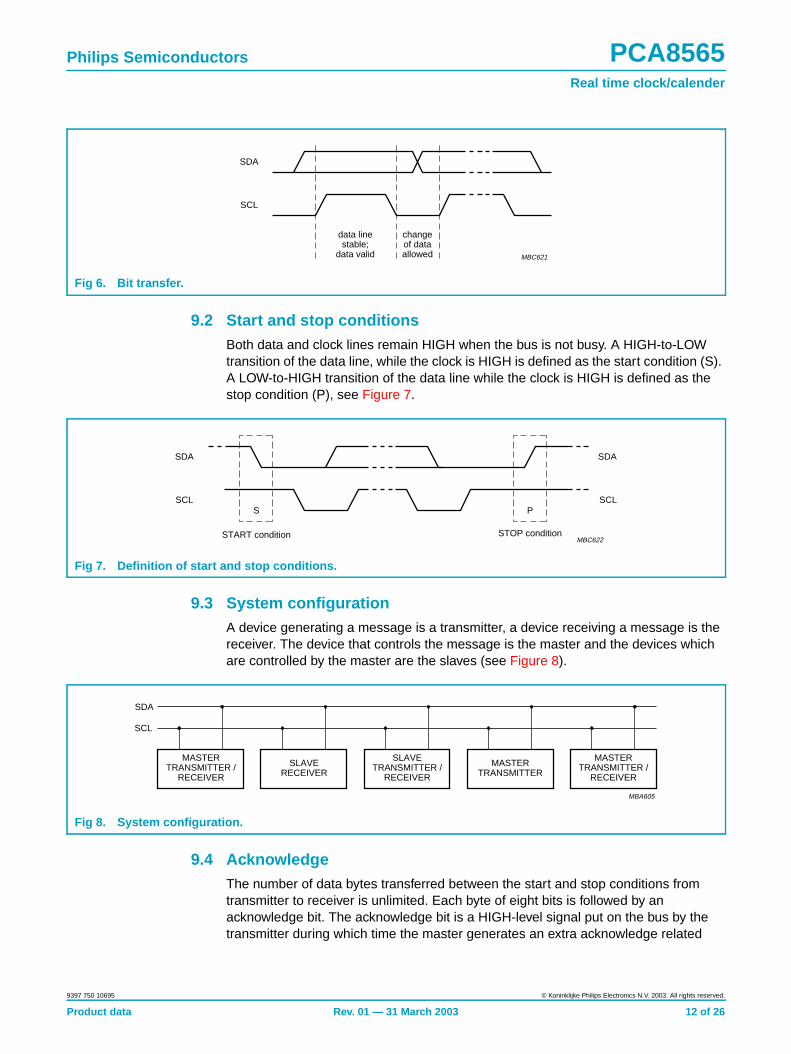
9.1 Bit transferOne data bit is transferred during each clock pulse. The data on the SDA line mustremain stable during the HIGH period of the clock pulse as changes in the data line atthis time will be interpreted as a control signal (see Figure 6).
Fig 5. POR override sequence.
handbook, full pagewidth
MGM664
SCL
500 ns 2000 ns
SDA
8 ms
override activepower up
Product data Rev. 01 — 31 March 2003 11 of 26
9397 750 10695 © Koninklijke Philips Electronics N.V. 2003. All rights reserved.
Philips Semiconductors PCA8565Real time clock/calender
9.2 Start and stop conditionsBoth data and clock lines remain HIGH when the bus is not busy. A HIGH-to-LOWtransition of the data line, while the clock is HIGH is defined as the start condition (S).A LOW-to-HIGH transition of the data line while the clock is HIGH is defined as thestop condition (P), see Figure 7.
9.3 System configurationA device generating a message is a transmitter, a device receiving a message is thereceiver. The device that controls the message is the master and the devices whichare controlled by the master are the slaves (see Figure 8).
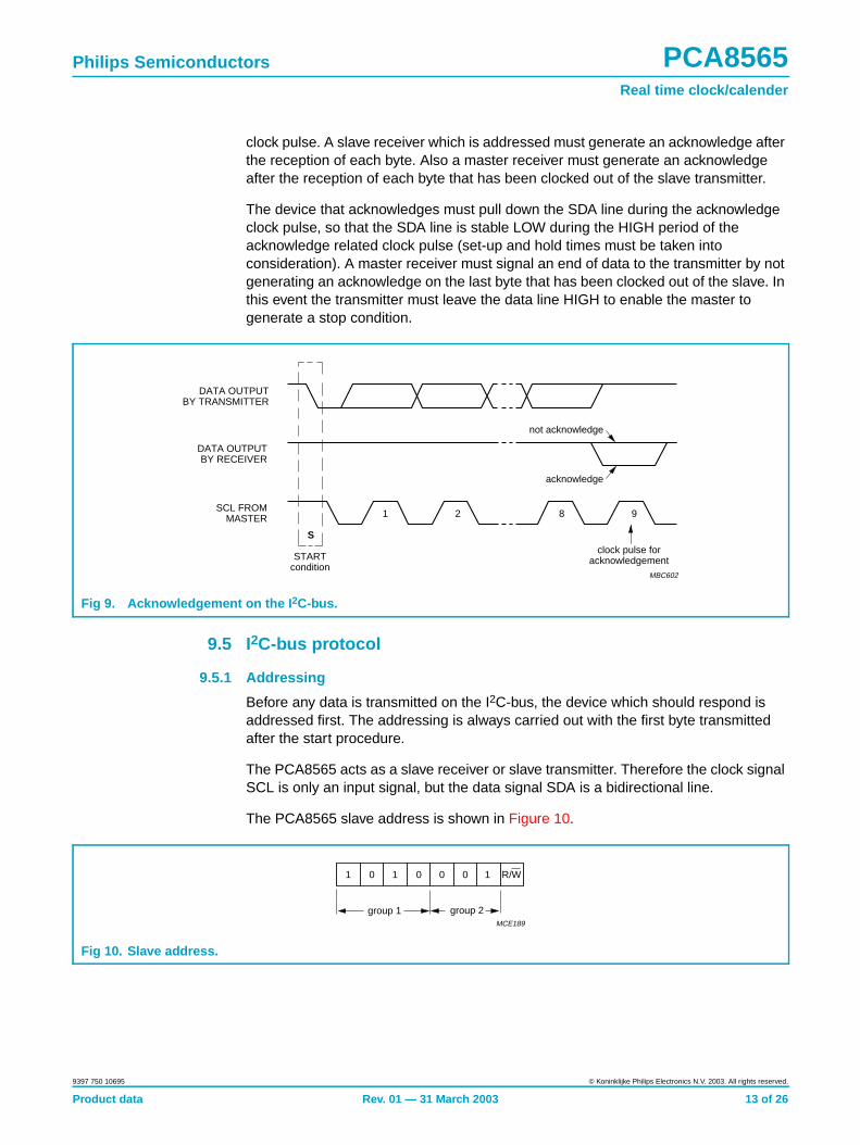
9.4 AcknowledgeThe number of data bytes transferred between the start and stop conditions fromtransmitter to receiver is unlimited. Each byte of eight bits is followed by anacknowledge bit. The acknowledge bit is a HIGH-level signal put on the bus by thetransmitter during which time the master generates an extra acknowledge related
Fig 6. Bit transfer.
MBC621
data linestable;
data valid
changeof dataallowed
SDA
SCL
Fig 7. Definition of start and stop conditions.
MBC622
SDA
SCLP
STOP condition
SDA
SCLS
START condition
Fig 8. System configuration.
MBA605
MASTERTRANSMITTER /
RECEIVER
SLAVERECEIVER
SLAVETRANSMITTER /
RECEIVER
MASTERTRANSMITTER
MASTERTRANSMITTER /
RECEIVER
SDA
SCL
Product data Rev. 01 — 31 March 2003 12 of 26
9397 750 10695 © Koninklijke Philips Electronics N.V. 2003. All rights reserved.
Philips Semiconductors PCA8565Real time clock/calender
clock pulse. A slave receiver which is addressed must generate an acknowledge afterthe reception of each byte. Also a master receiver must generate an acknowledgeafter the reception of each byte that has been clocked out of the slave transmitter.
The device that acknowledges must pull down the SDA line during the acknowledgeclock pulse, so that the SDA line is stable LOW during the HIGH period of theacknowledge related clock pulse (set-up and hold times must be taken intoconsideration). A master receiver must signal an end of data to the transmitter by notgenerating an acknowledge on the last byte that has been clocked out of the slave. Inthis event the transmitter must leave the data line HIGH to enable the master togenerate a stop condition.
9.5 I2C-bus protocol
9.5.1 Addressing
Before any data is transmitted on the I2C-bus, the device which should respond isaddressed first. The addressing is always carried out with the first byte transmittedafter the start procedure.
The PCA8565 acts as a slave receiver or slave transmitter. Therefore the clock signalSCL is only an input signal, but the data signal SDA is a bidirectional line.
The PCA8565 slave address is shown in Figure 10.
Fig 9. Acknowledgement on the I 2C-bus.
MBC602
S
STARTcondition
9821
clock pulse foracknowledgement
not acknowledge
acknowledge
DATA OUTPUTBY TRANSMITTER
DATA OUTPUTBY RECEIVER
SCL FROMMASTER
Fig 10. Slave address.
MCE189
1 0 1 0 0 0 1 R/W
group 1 group 2
Product data Rev. 01 — 31 March 2003 13 of 26
9397 750 10695 © Koninklijke Philips Electronics N.V. 2003. All rights reserved.
Philips Semiconductors PCA8565Real time clock/calender
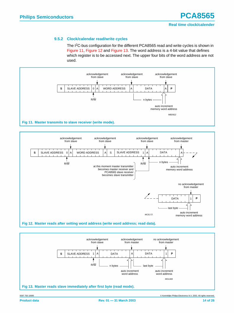
9.5.2 Clock/calendar read/write cycles
The I2C-bus configuration for the different PCA8565 read and write cycles is shown inFigure 11, Figure 12 and Figure 13. The word address is a 4-bit value that defineswhich register is to be accessed next. The upper four bits of the word address are notused.
Fig 11. Master transmits to slave receiver (write mode).
S 0 ASLAVE ADDRESS WORD ADDRESS A ADATA P
acknowledgementfrom slave
acknowledgementfrom slave
acknowledgementfrom slave
R/W
auto incrementmemory word address
MBD822
n bytes
Fig 12. Master reads after setting word address (write word address; read data).
S 0 ASLAVE ADDRESS WORD ADDRESS A ASLAVE ADDRESS
acknowledgementfrom slave
acknowledgementfrom slave
acknowledgementfrom slave
R/W
acknowledgementfrom master
ADATA
auto incrementmemory word address
MCE172
P
no acknowledgementfrom master
1DATA
auto incrementmemory word address
last byte
R/W
S 1
n bytes
at this moment master transmitterbecomes master receiver and
PCA8565 slave receiverbecomes slave transmitter
Fig 13. Master reads slave immediately after first byte (read mode).
handbook, full pagewidth
S 1 ASLAVE ADDRESS DATA A 1DATA
acknowledgementfrom slave
acknowledgementfrom master
no acknowledgementfrom master
R/W
auto incrementword address
MGL665
auto incrementword address
n bytes last byte
P
Product data Rev. 01 — 31 March 2003 14 of 26
9397 750 10695 © Koninklijke Philips Electronics N.V. 2003. All rights reserved.
Philips Semiconductors PCA8565Real time clock/calender
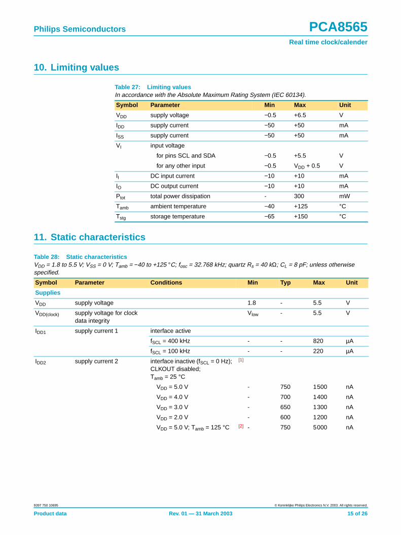
10. Limiting values
11. Static characteristics
Table 27: Limiting valuesIn accordance with the Absolute Maximum Rating System (IEC 60134).
Symbol Parameter Min Max Unit
VDD supply voltage −0.5 +6.5 V
IDD supply current −50 +50 mA
ISS supply current −50 +50 mA
VI input voltage
for pins SCL and SDA −0.5 +5.5 V
for any other input −0.5 VDD + 0.5 V
II DC input current −10 +10 mA
IO DC output current −10 +10 mA
Ptot total power dissipation - 300 mW
Tamb ambient temperature −40 +125 °C
Tstg storage temperature −65 +150 °C
Table 28: Static characteristicsVDD = 1.8 to 5.5 V; VSS = 0 V; Tamb = −40 to +125 °C; fosc = 32.768 kHz; quartz Rs = 40 kΩ; CL = 8 pF; unless otherwisespecified.
Symbol Parameter Conditions Min Typ Max Unit
Supplies
VDD supply voltage 1.8 - 5.5 V
VDD(clock) supply voltage for clockdata integrity
Vlow - 5.5 V
IDD1 supply current 1 interface active
fSCL = 400 kHz - - 820 µA
fSCL = 100 kHz - - 220 µA
IDD2 supply current 2 interface inactive (fSCL = 0 Hz);CLKOUT disabled;Tamb = 25 °C
[1]
VDD = 5.0 V - 750 1500 nA
VDD = 4.0 V - 700 1400 nA
VDD = 3.0 V - 650 1300 nA
VDD = 2.0 V - 600 1200 nA
VDD = 5.0 V; Tamb = 125 °C [2] - 750 5000 nA
Product data Rev. 01 — 31 March 2003 15 of 26
9397 750 10695 © Koninklijke Philips Electronics N.V. 2003. All rights reserved.
Philips Semiconductors PCA8565Real time clock/calender
[1] Timer source clock = 1⁄60 Hz, level of pins SCL and SDA is VDD or VSS.
[2] Worst case is at high temperature and high supply voltage.
[3] Timer source clock = 1⁄60 Hz, level of pins SCL and SDA is VDD or VSS.
[4] Tested on sample basis.
IDD3 supply current 3 interface inactive (fSCL = 0 Hz);CLKOUT enabled at 32 kHz;Tamb = 25 °C
[3]
VDD = 5.0 V - 1000 2000 nA
VDD = 4.0 V - 900 1800 nA
VDD = 3.0 V - 800 1600 nA
VDD = 2.0 V - 700 1400 nA
VDD = 5.0 V;Tamb = 125 °C [2] - 1000 6000 nA
Inputs
VIL LOW-level input voltage VSS − 0.3 - 0.3VDD V
VIH(SCL) SCL HIGH-level inputvoltage
0.7VDD - 5.5 V
VIH(SDA) SDA HIGH-level inputvoltage
0.7VDD - 5.5 V
VIH(OSCI) OSCI HIGH-level inputvoltage
0.7VDD - VDD + 0.3 V
ILI(SCL) SCL input leakage current VI = VDD or VSS −1 0 +1 µA
ILI(SDA) SDA input leakage current VI = VDD or VSS −1 0 +1 µA
Ci input capacitance [4] - - 7 pF
Outputs
IOL(SDA) SDA LOW-level outputcurrent
VOL = 0.4 V; VDD = 5 V −3 - - mA
IOL(INT) INT LOW-level outputcurrent
VOL = 0.4 V; VDD = 5 V −1 - - mA
IOL(CLKOUT) CLKOUT LOW-leveloutput current
VO = VDD or VSS −1 - - mA
ILO output leakage current −1 0 +1 µA
Voltage detector
Vlow low voltage detection - 0.9 1.7 V
Temperature
Tamb ambient temperature −40 +125 °C
Table 28: Static characteristics …continuedVDD = 1.8 to 5.5 V; VSS = 0 V; Tamb = −40 to +125 °C; fosc = 32.768 kHz; quartz Rs = 40 kΩ; CL = 8 pF; unless otherwisespecified.
Symbol Parameter Conditions Min Typ Max Unit
Product data Rev. 01 — 31 March 2003 16 of 26
9397 750 10695 © Koninklijke Philips Electronics N.V. 2003. All rights reserved.
Philips Semiconductors PCA8565Real time clock/calender
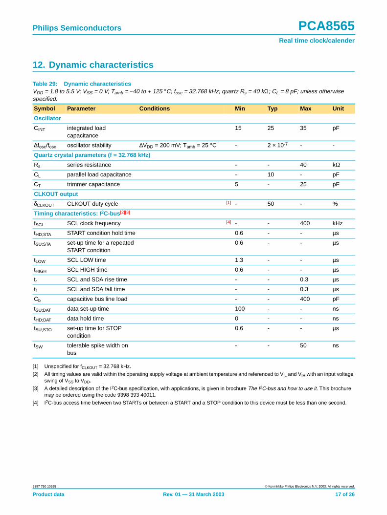
12. Dynamic characteristics
[1] Unspecified for fCLKOUT = 32.768 kHz.
[2] All timing values are valid within the operating supply voltage at ambient temperature and referenced to VIL and VIH with an input voltageswing of VSS to VDD.
[3] A detailed description of the I2C-bus specification, with applications, is given in brochure The I2C-bus and how to use it. This brochuremay be ordered using the code 9398 393 40011.
[4] I2C-bus access time between two STARTs or between a START and a STOP condition to this device must be less than one second.
Table 29: Dynamic characteristicsVDD = 1.8 to 5.5 V; VSS = 0 V; Tamb = −40 to + 125 °C; fosc = 32.768 kHz; quartz Rs = 40 kΩ; CL = 8 pF; unless otherwisespecified.
Symbol Parameter Conditions Min Typ Max Unit
Oscillator
CINT integrated loadcapacitance
15 25 35 pF
∆fosc/fosc oscillator stability ∆VDD = 200 mV; Tamb = 25 °C - 2 × 10⁻⁷ - -
Quartz crystal parameters (f = 32.768 kHz)
Rs series resistance - - 40 kΩ
CL parallel load capacitance - 10 - pF
CT trimmer capacitance 5 - 25 pF
CLKOUT output
δCLKOUT CLKOUT duty cycle [1] - 50 - %
Timing characteristics: I 2C-bus [2][3]
fSCL SCL clock frequency [4] - - 400 kHz
tHD;STA START condition hold time 0.6 - - µs
tSU;STA set-up time for a repeatedSTART condition
0.6 - - µs
tLOW SCL LOW time 1.3 - - µs
tHIGH SCL HIGH time 0.6 - - µs
tr SCL and SDA rise time - - 0.3 µs
tf SCL and SDA fall time - - 0.3 µs
Cb capacitive bus line load - - 400 pF
tSU;DAT data set-up time 100 - - ns
tHD;DAT data hold time 0 - - ns
tSU;STO set-up time for STOPcondition
0.6 - - µs
tSW tolerable spike width onbus
- - 50 ns
Product data Rev. 01 — 31 March 2003 17 of 26
9397 750 10695 © Koninklijke Philips Electronics N.V. 2003. All rights reserved.
Philips Semiconductors PCA8565Real time clock/calender
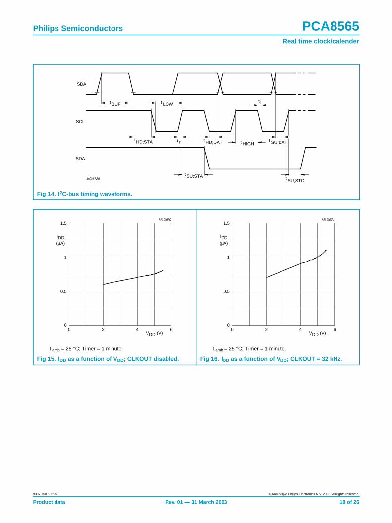
Fig 14. I2C-bus timing waveforms.
SDA
MGA728
SDA
SCL
tSU;STA t SU;STO
tHD;STA
t BUF t LOW
t HD;DAT t HIGHt r
t f
t SU;DAT
Tamb = 25 °C; Timer = 1 minute. Tamb = 25 °C; Timer = 1 minute.
Fig 15. IDD as a function of V DD; CLKOUT disabled. Fig 16. I DD as a function of V DD; CLKOUT = 32 kHz.
0
1.5
1
0.5
02 4 6
MLD970
VDD (V)
IDD(µA)
0
1.5
1
0.5
02 4 6
MLD971
VDD (V)
IDD(µA)
Product data Rev. 01 — 31 March 2003 18 of 26
9397 750 10695 © Koninklijke Philips Electronics N.V. 2003. All rights reserved.
Philips Semiconductors PCA8565Real time clock/calender
13. Application information
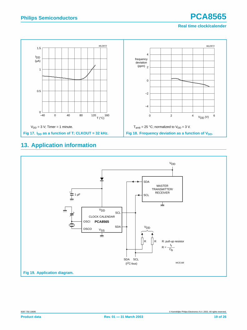
VDD = 3 V; Timer = 1 minute. Tamb = 25 °C; normalized to VDD = 3 V.
Fig 17. IDD as a function of T; CLKOUT = 32 kHz. Fig 18. Frequency deviation as a function of V DD.
−40
1.5
1
0.5
00 16040 80 120
MLD972
T (°C)
IDD(µA)
0 2 6
4
2
−4
−2
0
MLD973
4 VDD (V)
frequencydeviation
(ppm)
Fig 19. Application diagram.
MCE168
SCL
SDAVSS
OSCI
OSCO
CLOCK CALENDAR
PCA8565
SDA
SCL
MASTERTRANSMITTER/
RECEIVER
VDD
VDD
SDA SCL
R R
VDD
(I2C-bus)
R: pull-up resistor
R =
1 µF
trCb
Product data Rev. 01 — 31 March 2003 19 of 26
9397 750 10695 © Koninklijke Philips Electronics N.V. 2003. All rights reserved.
Philips Semiconductors PCA8565Real time clock/calender
13.1 Quartz frequency adjustment
13.1.1 Method 1: fixed OSCI capacitor
By evaluating the average capacitance necessary for the application layout, a fixedcapacitor can be used. The frequency is best measured via the 32.768 kHz signalavailable after power-on at pin CLKOUT. The frequency tolerance depends on thequartz crystal tolerance, the capacitor tolerance and the device-to-device tolerance(on average ±5 × 10⁻⁶). Average deviations of ±5 minutes per year can be easilyachieved.
13.1.2 Method 2: OSCI trimmer
Using the 32.768 kHz signal available after power-on at pin CLKOUT, fast setting of atrimmer is possible.
13.1.3 Method 3: OSCO output
Direct measurement of OSCO out (accounting for test probe capacitance).
Product data Rev. 01 — 31 March 2003 20 of 26
9397 750 10695 © Koninklijke Philips Electronics N.V. 2003. All rights reserved.
Philips Semiconductors PCA8565Real time clock/calender
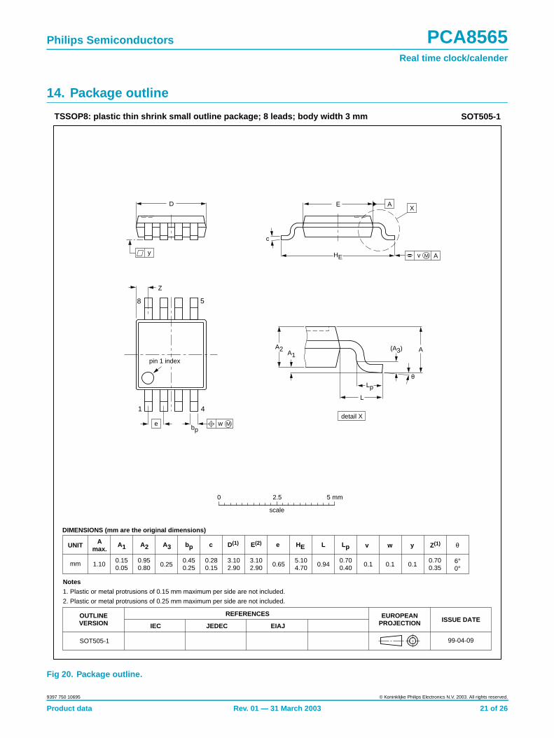
14. Package outline
Fig 20. Package outline.
UNIT A1A
max.A2 A3 bp LHE Lp w yvc eD(1) E(2) Z(1) θ
REFERENCESOUTLINEVERSION
EUROPEANPROJECTION ISSUE DATE
IEC JEDEC EIAJ
mm 0.150.05
0.950.80
0.450.25
0.280.15
3.102.90
3.102.90 0.65
5.104.70
0.700.35
6°0°0.1 0.10.10.94
DIMENSIONS (mm are the original dimensions)
Notes
1. Plastic or metal protrusions of 0.15 mm maximum per side are not included.
2. Plastic or metal protrusions of 0.25 mm maximum per side are not included.
0.700.40
SOT505-1 99-04-09
w Mbp
D
Z
e
0.25
1 4
8 5
θ
AA2A1
Lp
(A3)
detail X
L
HE
E
c
v M A
XA
y
2.5 5 mm0
scale
TSSOP8: plastic thin shrink small outline package; 8 leads; body width 3 mm SOT505-1
1.10
pin 1 index
Product data Rev. 01 — 31 March 2003 21 of 26
9397 750 10695 © Koninklijke Philips Electronics N.V. 2003. All rights reserved.
Philips Semiconductors PCA8565Real time clock/calender
15. Soldering
15.1 Introduction to soldering surface mount packagesThis text gives a very brief insight to a complex technology. A more in-depth accountof soldering ICs can be found in our Data Handbook IC26; Integrated CircuitPackages (document order number 9398 652 90011).
There is no soldering method that is ideal for all surface mount IC packages. Wavesoldering can still be used for certain surface mount ICs, but it is not suitable for finepitch SMDs. In these situations reflow soldering is recommended.
15.2 Reflow solderingReflow soldering requires solder paste (a suspension of fine solder particles, flux andbinding agent) to be applied to the printed-circuit board by screen printing, stencillingor pressure-syringe dispensing before package placement.
Several methods exist for reflowing; for example, convection or convection/infraredheating in a conveyor type oven. Throughput times (preheating, soldering andcooling) vary between 100 and 200 seconds depending on heating method.
Typical reflow peak temperatures range from 215 to 250 °C. The top-surfacetemperature of the packages should preferably be kept:
• below 220 °C for all the BGA packages and packages with a thickness ≥ 2.5mmand packages with a thickness <2.5 mm and a volume ≥350 mm3 so calledthick/large packages
• below 235 °C for packages with a thickness <2.5 mm and a volume <350 mm3 socalled small/thin packages.
15.3 Wave solderingConventional single wave soldering is not recommended for surface mount devices(SMDs) or printed-circuit boards with a high component density, as solder bridgingand non-wetting can present major problems.
To overcome these problems the double-wave soldering method was specificallydeveloped.
If wave soldering is used the following conditions must be observed for optimalresults:
• Use a double-wave soldering method comprising a turbulent wave with highupward pressure followed by a smooth laminar wave.
• For packages with leads on two sides and a pitch (e):
– larger than or equal to 1.27 mm, the footprint longitudinal axis is preferred to beparallel to the transport direction of the printed-circuit board;
– smaller than 1.27 mm, the footprint longitudinal axis must be parallel to thetransport direction of the printed-circuit board.
The footprint must incorporate solder thieves at the downstream end.
Product data Rev. 01 — 31 March 2003 22 of 26
9397 750 10695 © Koninklijke Philips Electronics N.V. 2003. All rights reserved.
Philips Semiconductors PCA8565Real time clock/calender
• For packages with leads on four sides, the footprint must be placed at a 45° angleto the transport direction of the printed-circuit board. The footprint mustincorporate solder thieves downstream and at the side corners.
During placement and before soldering, the package must be fixed with a droplet ofadhesive. The adhesive can be applied by screen printing, pin transfer or syringedispensing. The package can be soldered after the adhesive is cured.
Typical dwell time is 4 seconds at 250 °C. A mildly-activated flux will eliminate theneed for removal of corrosive residues in most applications.
15.4 Manual solderingFix the component by first soldering two diagonally-opposite end leads. Use a lowvoltage (24 V or less) soldering iron applied to the flat part of the lead. Contact timemust be limited to 10 seconds at up to 300 °C.
When using a dedicated tool, all other leads can be soldered in one operation within2 to 5 seconds between 270 and 320 °C.
15.5 Package related soldering information
[1] For more detailed information on the BGA packages refer to the (LF)BGA Application Note(AN01026); order a copy from your Philips Semiconductors sales office.
[2] All surface mount (SMD) packages are moisture sensitive. Depending upon the moisture content, themaximum temperature (with respect to time) and body size of the package, there is a risk that internalor external package cracks may occur due to vaporization of the moisture in them (the so calledpopcorn effect). For details, refer to the Drypack information in the Data Handbook IC26; IntegratedCircuit Packages; Section: Packing Methods.
[3] These packages are not suitable for wave soldering. On versions with the heatsink on the bottomside, the solder cannot penetrate between the printed-circuit board and the heatsink. On versions withthe heatsink on the top side, the solder might be deposited on the heatsink surface.
[4] If wave soldering is considered, then the package must be placed at a 45° angle to the solder wavedirection. The package footprint must incorporate solder thieves downstream and at the side corners.
[5] Wave soldering is suitable for LQFP, QFP and TQFP packages with a pitch (e) larger than 0.8 mm; itis definitely not suitable for packages with a pitch (e) equal to or smaller than 0.65 mm.
[6] Wave soldering is suitable for SSOP and TSSOP packages with a pitch (e) equal to or larger than0.65 mm; it is definitely not suitable for packages with a pitch (e) equal to or smaller than 0.5 mm.
Table 30: Suitability of surface mount IC packages for wave and reflow solderingmethods
Package [1] Soldering method
Wave Reflow [2]
BGA, LBGA, LFBGA, SQFP, TFBGA, VFBGA not suitable suitable
DHVQFN, HBCC, HBGA, HLQFP, HSQFP,HSOP, HTQFP, HTSSOP, HVQFN, HVSON,SMS
not suitable[3] suitable
PLCC[4], SO, SOJ suitable suitable
LQFP, QFP, TQFP not recommended[4][5] suitable
SSOP, TSSOP, VSO, VSSOP not recommended[6] suitable
Product data Rev. 01 — 31 March 2003 23 of 26
9397 750 10695 © Koninklijke Philips Electronics N.V. 2003. All rights reserved.
Philips Semiconductors PCA8565Real time clock/calender
16. Revision history
Table 31: Revision history
Rev Date CPCN Description
01 20030331 - Product data (9397 750 10695)
Product data Rev. 01 — 31 March 2003 24 of 26
9397 750 10695 © Koninklijke Philips Electronics N.V. 2003. All rights reserved.
Philips Semiconductors PCA8565Real time clock/calender
17. Data sheet status
[1] Please consult the most recently issued data sheet before initiating or completing a design.
[2] The product status of the device(s) described in this data sheet may have changed since this data sheet was published. The latest information is available on the Internet atURL http://www.semiconductors.philips.com.
[3] For data sheets describing multiple type numbers, the highest-level product status determines the data sheet status.
18. Definitions
Short-form specification — The data in a short-form specification isextracted from a full data sheet with the same type number and title. Fordetailed information see the relevant data sheet or data handbook.
Limiting values definition — Limiting values given are in accordance withthe Absolute Maximum Rating System (IEC 60134). Stress above one ormore of the limiting values may cause permanent damage to the device.These are stress ratings only and operation of the device at these or at anyother conditions above those given in the Characteristics sections of thespecification is not implied. Exposure to limiting values for extended periodsmay affect device reliability.
Application information — Applications that are described herein for anyof these products are for illustrative purposes only. Philips Semiconductorsmake no representation or warranty that such applications will be suitable forthe specified use without further testing or modification.
19. Disclaimers
Life support — These products are not designed for use in life supportappliances, devices, or systems where malfunction of these products canreasonably be expected to result in personal injury. Philips Semiconductors
customers using or selling these products for use in such applications do soat their own risk and agree to fully indemnify Philips Semiconductors for anydamages resulting from such application.
Right to make changes — Philips Semiconductors reserves the right tomake changes in the products - including circuits, standard cells, and/orsoftware - described or contained herein in order to improve design and/orperformance. When the product is in full production (status ‘Production’),relevant changes will be communicated via a Customer Product/ProcessChange Notification (CPCN). Philips Semiconductors assumes noresponsibility or liability for the use of any of these products, conveys nolicence or title under any patent, copyright, or mask work right to theseproducts, and makes no representations or warranties that these products arefree from patent, copyright, or mask work right infringement, unless otherwisespecified.
20. Licenses
Level Data sheet status [1] Product status [2][3] Definition
I Objective data Development This data sheet contains data from the objective specification for product development. PhilipsSemiconductors reserves the right to change the specification in any manner without notice.
II Preliminary data Qualification This data sheet contains data from the preliminary specification. Supplementary data will be publishedat a later date. Philips Semiconductors reserves the right to change the specification without notice, inorder to improve the design and supply the best possible product.
III Product data Production This data sheet contains data from the product specification. Philips Semiconductors reserves theright to make changes at any time in order to improve the design, manufacturing and supply. Relevantchanges will be communicated via a Customer Product/Process Change Notification (CPCN).
Purchase of Philips I 2C components
Purchase of Philips I2C components conveys a licenseunder the Philips’ I2C patent to use the components in theI2C system provided the system conforms to the I2Cspecification defined by Philips. This specification can beordered using the code 9398 393 40011.
9397 750 10695 © Koninklijke Philips Electronics N.V. 2003. All rights reserved.
Product data Rev. 01 — 31 March 2003 25 of 26
Contact informationFor additional information, please visit http://www.semiconductors.philips.com .For sales office addresses, send e-mail to: [email protected] . Fax: +31 40 27 24825
© Koninklijke Philips Electronics N.V. 2003.Printed in The Netherlands
All rights are reserved. Reproduction in whole or in part is prohibited without the priorwritten consent of the copyright owner.
The information presented in this document does not form part of any quotation orcontract, is believed to be accurate and reliable and may be changed without notice. Noliability will be accepted by the publisher for any consequence of its use. Publicationthereof does not convey nor imply any license under patent- or other industrial orintellectual property rights.
Date of release: 31 March 2003 Document order number: 9397 750 10695
Contents
Philips Semiconductors PCA8565Real time clock/calender
1 General description . . . . . . . . . . . . . . . . . . . . . . 12 Features . . . . . . . . . . . . . . . . . . . . . . . . . . . . . . . 13 Applications . . . . . . . . . . . . . . . . . . . . . . . . . . . . 14 Quick reference data . . . . . . . . . . . . . . . . . . . . . 15 Ordering information . . . . . . . . . . . . . . . . . . . . . 26 Block diagram . . . . . . . . . . . . . . . . . . . . . . . . . . 27 Pinning information . . . . . . . . . . . . . . . . . . . . . . 27.1 Pinning . . . . . . . . . . . . . . . . . . . . . . . . . . . . . . . 27.2 Pin description . . . . . . . . . . . . . . . . . . . . . . . . . 38 Functional description . . . . . . . . . . . . . . . . . . . 38.1 Alarm function modes. . . . . . . . . . . . . . . . . . . . 48.2 Timer. . . . . . . . . . . . . . . . . . . . . . . . . . . . . . . . . 48.3 CLKOUT output . . . . . . . . . . . . . . . . . . . . . . . . 48.4 Reset . . . . . . . . . . . . . . . . . . . . . . . . . . . . . . . . 48.5 Voltage-low detector . . . . . . . . . . . . . . . . . . . . . 48.6 Register organization . . . . . . . . . . . . . . . . . . . . 58.6.1 Control/status 1 register . . . . . . . . . . . . . . . . . . 68.6.2 Control/status 2 register . . . . . . . . . . . . . . . . . . 68.6.3 Time and date registers . . . . . . . . . . . . . . . . . . 78.6.4 Alarm registers . . . . . . . . . . . . . . . . . . . . . . . . . 88.6.5 CLOCKOUT control register . . . . . . . . . . . . . . . 98.6.6 Countdown timer. . . . . . . . . . . . . . . . . . . . . . . . 98.7 EXT_CLK test mode. . . . . . . . . . . . . . . . . . . . 108.8 Power-On Reset (POR) override . . . . . . . . . . 119 Characteristics of the I 2C-bus. . . . . . . . . . . . . 119.1 Bit transfer . . . . . . . . . . . . . . . . . . . . . . . . . . . 119.2 Start and stop conditions . . . . . . . . . . . . . . . . 129.3 System configuration . . . . . . . . . . . . . . . . . . . 129.4 Acknowledge . . . . . . . . . . . . . . . . . . . . . . . . . 129.5 I2C-bus protocol . . . . . . . . . . . . . . . . . . . . . . . 139.5.1 Addressing . . . . . . . . . . . . . . . . . . . . . . . . . . . 139.5.2 Clock/calendar read/write cycles . . . . . . . . . . 1410 Limiting values. . . . . . . . . . . . . . . . . . . . . . . . . 1511 Static characteristics. . . . . . . . . . . . . . . . . . . . 1512 Dynamic characteristics . . . . . . . . . . . . . . . . . 1713 Application information. . . . . . . . . . . . . . . . . . 1913.1 Quartz frequency adjustment . . . . . . . . . . . . . 2013.1.1 Method 1: fixed OSCI capacitor . . . . . . . . . . . 2013.1.2 Method 2: OSCI trimmer. . . . . . . . . . . . . . . . . 2013.1.3 Method 3: OSCO output . . . . . . . . . . . . . . . . . 2014 Package outline . . . . . . . . . . . . . . . . . . . . . . . . 2115 Soldering . . . . . . . . . . . . . . . . . . . . . . . . . . . . . 2215.1 Introduction to soldering surface mount
packages . . . . . . . . . . . . . . . . . . . . . . . . . . . . 2215.2 Reflow soldering . . . . . . . . . . . . . . . . . . . . . . . 2215.3 Wave soldering . . . . . . . . . . . . . . . . . . . . . . . . 2215.4 Manual soldering . . . . . . . . . . . . . . . . . . . . . . 23
15.5 Package related soldering information . . . . . . 2316 Revision history . . . . . . . . . . . . . . . . . . . . . . . 2417 Data sheet status. . . . . . . . . . . . . . . . . . . . . . . 2518 Definitions . . . . . . . . . . . . . . . . . . . . . . . . . . . . 2519 Disclaimers . . . . . . . . . . . . . . . . . . . . . . . . . . . 2520 Licenses . . . . . . . . . . . . . . . . . . . . . . . . . . . . . . 25

This datasheet has been download from:
www.datasheetcatalog.com
Datasheets for electronics components.