Embed Size (px)
Citation preview
1 BROOKHAVEN SCIENCE ASSOCIATES
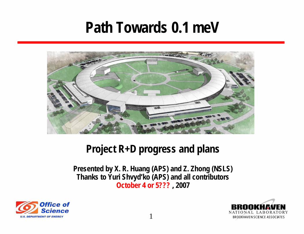
Path Towards 0.1 meV
Project R+D progress and plansPresented by X. R. Huang (APS) and Z. Zhong (NSLS)Thanks to Yuri Shvyd’ko (APS) and all contributors
October 4 or 5??? , 2007
2 BROOKHAVEN SCIENCE ASSOCIATES
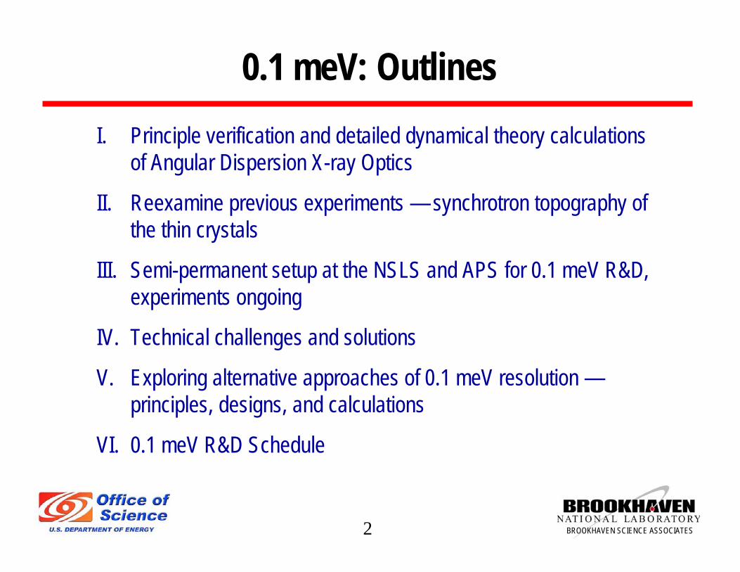
0.1 meV: OutlinesI. Principle verification and detailed dynamical theory calculations
of Angular Dispersion X-ray Optics
II. Reexamine previous experiments — synchrotron topography of the thin crystals
III. Semi-permanent setup at the NSLS and APS for 0.1 meV R&D, experiments ongoing
IV. Technical challenges and solutions
V. Exploring alternative approaches of 0.1 meV resolution —principles, designs, and calculations
VI. 0.1 meV R&D Schedule
3 BROOKHAVEN SCIENCE ASSOCIATES
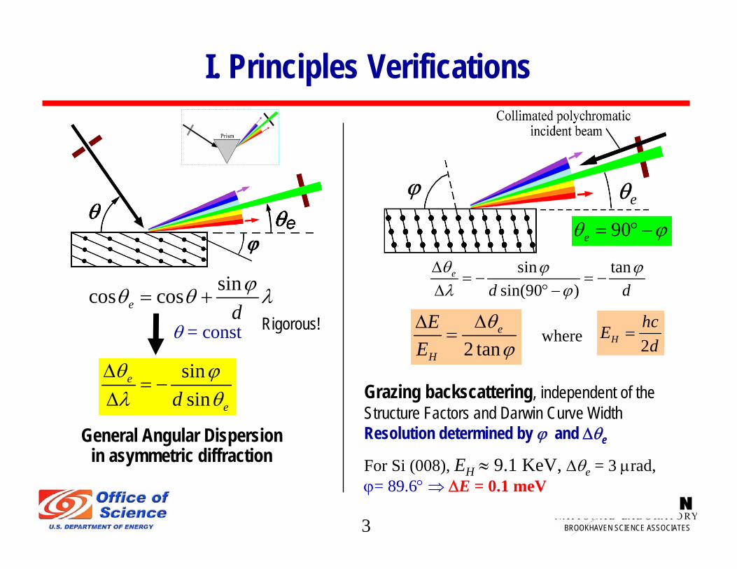
I. Principles Verifications
sincos cose dϕθ θ λ= +
sinsin
e
edθ ϕλ θ
Δ= −
Δ
θ = const
General Angular Dispersion in asymmetric diffraction
θeϕ
sin tansin(90 )
e
d dθ ϕ ϕλ ϕ
Δ= − = −
Δ °−
2 tane
H
EE
θϕ
ΔΔ= 2H
hcEd
=where
90eθ ϕ= °−
Grazing backscattering, independent of the Structure Factors and Darwin Curve Width Resolution determined by ϕ and Δθe
For Si (008), EH ≈ 9.1 KeV, Δθe = 3 μrad,ϕ= 89.6° ⇒ ΔE = 0.1 meV
Rigorous!
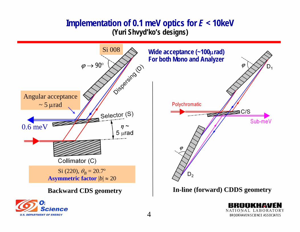
4 BROOKHAVEN SCIENCE ASSOCIATES
Implementation of 0.1 meV optics for E < 10keV (Yuri Shvyd’ko’s designs)
Si (220), θB = 20.7°Asymmetric factor |b| ≈ 20
Si 008
Angular acceptance~ 5 μrad
0.6 meV
Backward CDS geometry In-line (forward) CDDS geometry
Wide acceptance (~100μrad)For both Mono and Analyzer
ϕ→ 90°
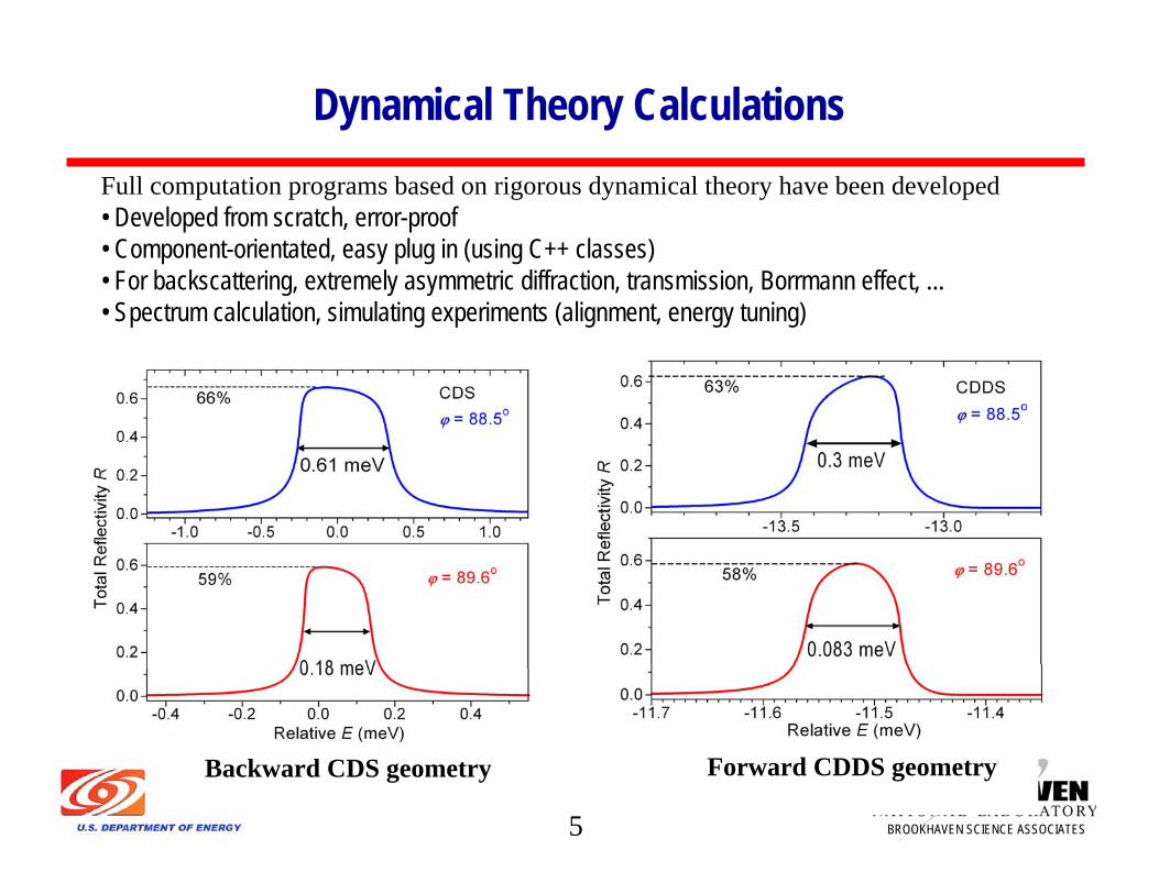
5 BROOKHAVEN SCIENCE ASSOCIATES
Dynamical Theory CalculationsFull computation programs based on rigorous dynamical theory have been developed• Developed from scratch, error-proof• Component-orientated, easy plug in (using C++ classes)• For backscattering, extremely asymmetric diffraction, transmission, Borrmann effect, ...• Spectrum calculation, simulating experiments (alignment, energy tuning)
Backward CDS geometry Forward CDDS geometry
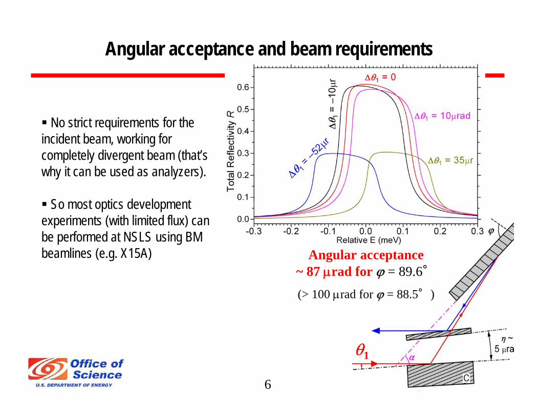
6 BROOKHAVEN SCIENCE ASSOCIATES
θ1
Angular acceptance and beam requirements
Angular acceptance~ 87 μrad for ϕ = 89.6°(> 100 μrad for ϕ = 88.5°)
No strict requirements for the incident beam, working for completely divergent beam (that’s why it can be used as analyzers).
So most optics development experiments (with limited flux) can be performed at NSLS using BM beamlines (e.g. X15A)
7 BROOKHAVEN SCIENCE ASSOCIATES
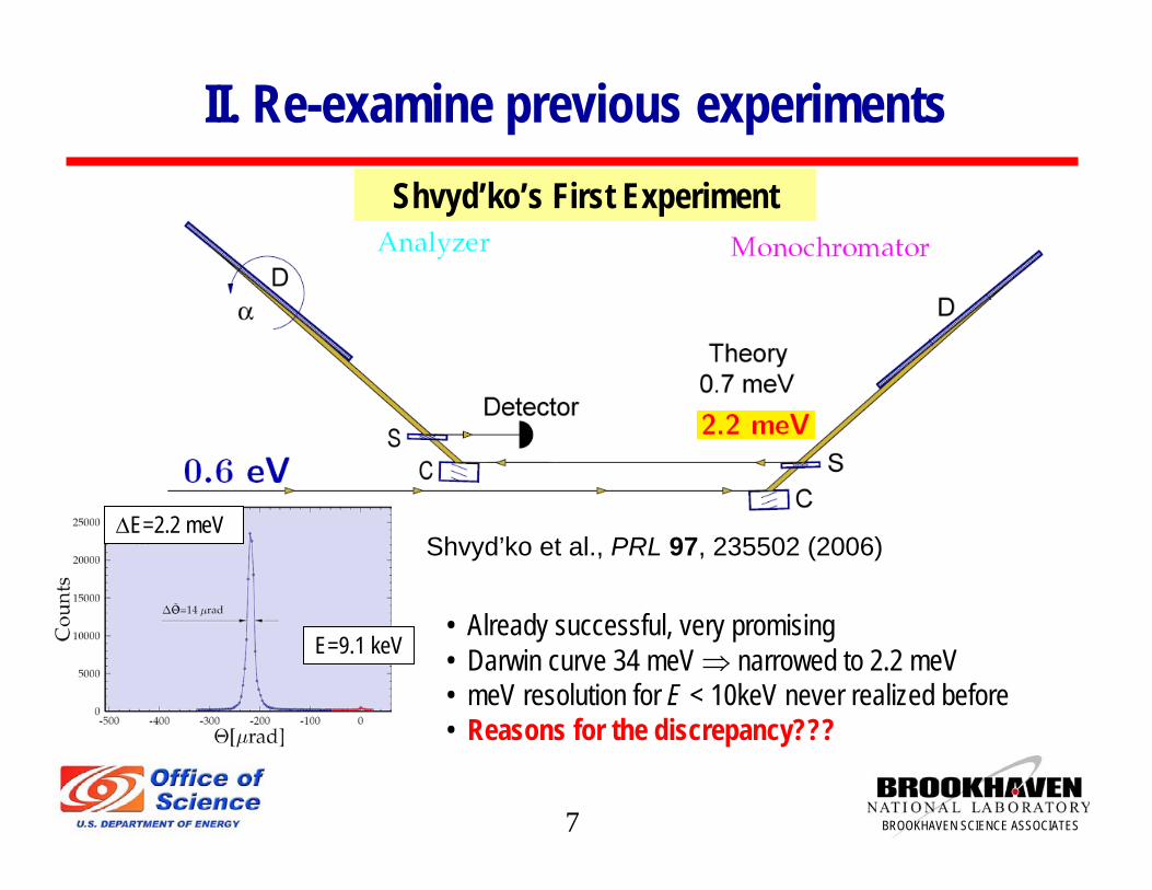
II. Re-examine previous experimentsShvyd’ko’s First Experiment
Shvyd’ko et al., PRL 97, 235502 (2006)
• Already successful, very promising• Darwin curve 34 meV ⇒ narrowed to 2.2 meV• meV resolution for E < 10keV never realized before • Reasons for the discrepancy???
E=9.1 keV
ΔE=2.2 meV
8 BROOKHAVEN SCIENCE ASSOCIATES
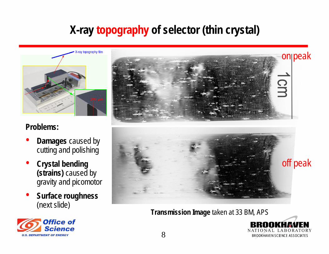
X-ray topography of selector (thin crystal)
on peak
off peak
Transmission Image taken at 33 BM, APS
Problems:• Damages caused by
cutting and polishing• Crystal bending
(strains) caused by gravity and picomotor
• Surface roughness (next slide)
9 BROOKHAVEN SCIENCE ASSOCIATES
X-ray topography (cont.)
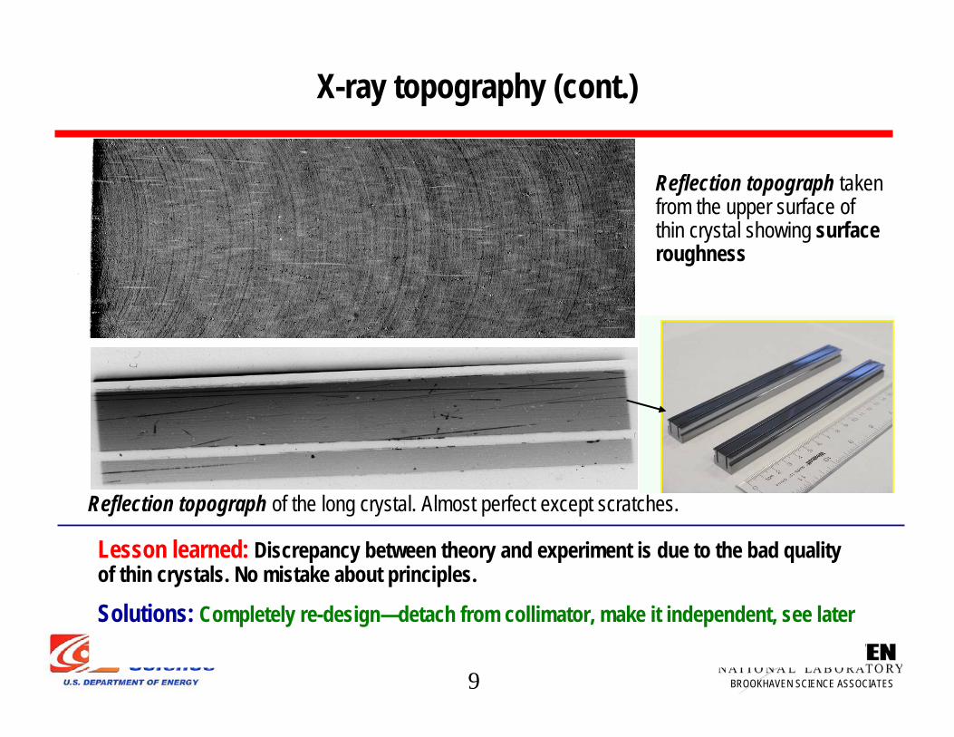
Reflection topograph taken from the upper surface of thin crystal showing surface roughness
Reflection topograph of the long crystal. Almost perfect except scratches.
Lesson learned: Discrepancy between theory and experiment is due to the bad quality of thin crystals. No mistake about principles.
Solutions: Completely re-design—detach from collimator, make it independent, see later
10 BROOKHAVEN SCIENCE ASSOCIATES
III. R+D ongoing
• Readily available x-rays is a NSLS advantage, a luxury for APS, ESRF and Spring-8
• A semi-permanent setup is attractive for serious experimentalists• Access may entice experts (such as Shvyd’ko) to come to BNL
more often• A playground may entice local experts (Siddons, Berman, Kao to
name a few) to roll up their sleeves, and play• Develops local expertise: one can only learn by doing, and making
mistakes
1. Semi-permanent optics development facilities at NSLS
11 BROOKHAVEN SCIENCE ASSOCIATES
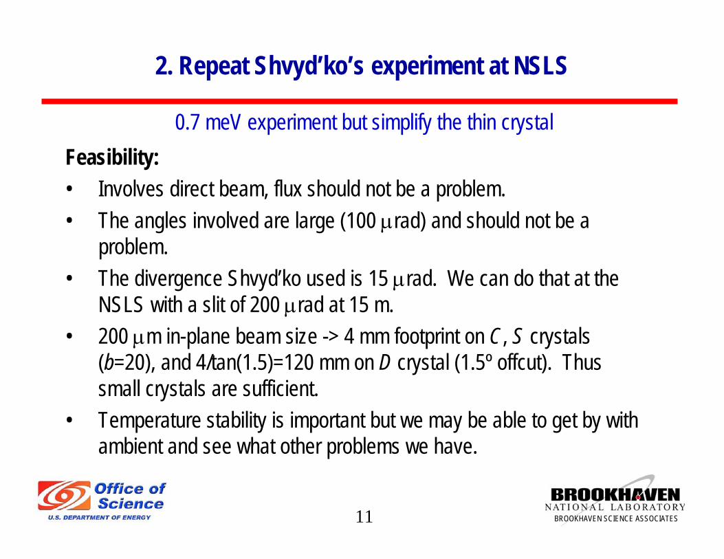
2. Repeat Shvyd’ko’s experiment at NSLS
Feasibility:• Involves direct beam, flux should not be a problem.• The angles involved are large (100 μrad) and should not be a
problem. • The divergence Shvyd’ko used is 15 μrad. We can do that at the
NSLS with a slit of 200 μrad at 15 m.• 200 μm in-plane beam size -> 4 mm footprint on C, S crystals
(b=20), and 4/tan(1.5)=120 mm on D crystal (1.5º offcut). Thus small crystals are sufficient.
• Temperature stability is important but we may be able to get by with ambient and see what other problems we have.
0.7 meV experiment but simplify the thin crystal
12 BROOKHAVEN SCIENCE ASSOCIATES
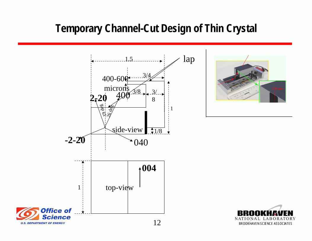
Temporary Channel-Cut Design of Thin Crystal
1
2-20
1 top-view
side-view
004
1.5
3/4
-2-20
400-600microns 3/
83/8
lap
1/8
400
040
26 d
eg19
deg
13 BROOKHAVEN SCIENCE ASSOCIATES
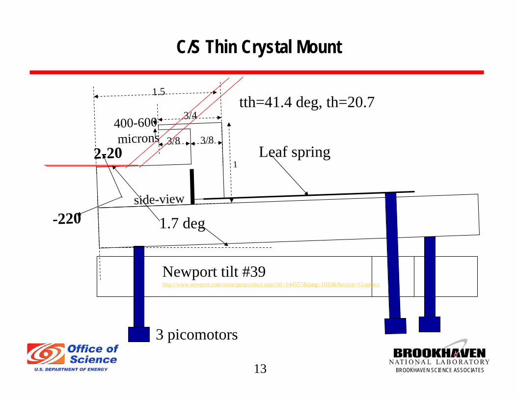
C/S Thin Crystal Mount
12-20
side-view
1.5
3/4
-220
400-600microns 3/83/8
1.7 deg
tth=41.4 deg, th=20.7
Leaf spring
Newport tilt #39http://www.newport.com/store/genproduct.aspx?id=144557&lang=1033&Section=Graphics
3 picomotors
14 BROOKHAVEN SCIENCE ASSOCIATES
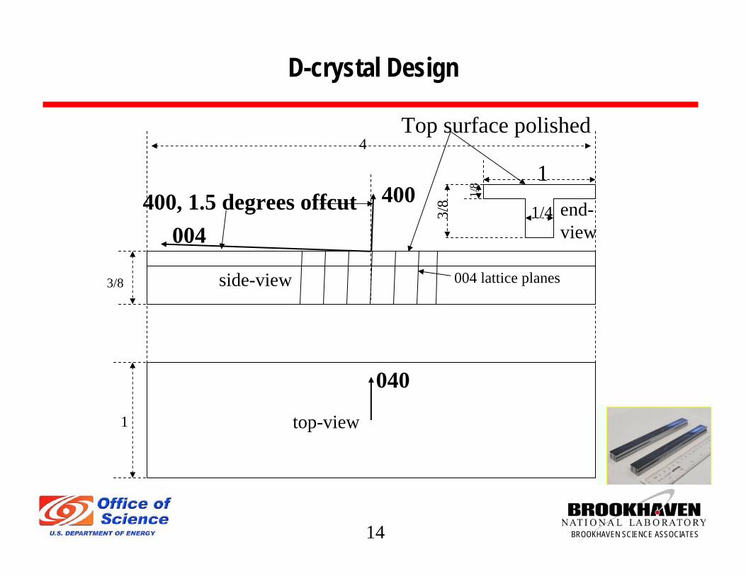
D-crystal Design
4
3/8
400400, 1.5 degrees offcut004
1 top-view
side-view
end-view
3/8
1
1/8
Top surface polished
040
004 lattice planes
1/4
15 BROOKHAVEN SCIENCE ASSOCIATES
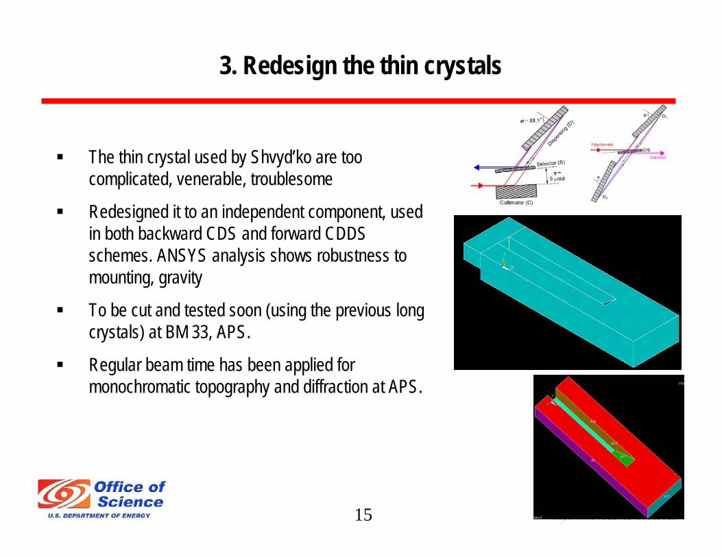
3. Redesign the thin crystals
The thin crystal used by Shvyd’ko are too complicated, venerable, troublesome
Redesigned it to an independent component, used in both backward CDS and forward CDDS schemes. ANSYS analysis shows robustness to mounting, gravity
To be cut and tested soon (using the previous long crystals) at BM 33, APS.
Regular beam time has been applied for monochromatic topography and diffraction at APS.
16 BROOKHAVEN SCIENCE ASSOCIATES
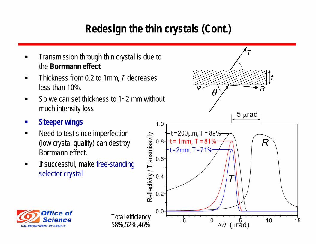
Redesign the thin crystals (Cont.)
Transmission through thin crystal is due to the Borrmann effectThickness from 0.2 to 1mm, T decreases less than 10%.So we can set thickness to 1~2 mm without much intensity lossSteeper wingsNeed to test since imperfection (low crystal quality) can destroy Borrmann effect.If successful, make free-standing selector crystal
θ
Total efficiency 58%,52%,46%
17 BROOKHAVEN SCIENCE ASSOCIATES
4. Crystal fabrication and characterization
Cutting, polishing, and etching all the necessary crystal components
Rocking curve measurements: strains, bending, surface quality
Topographic imaging: bending, roughness, defects
(at X19C, Mike Dudley’s topography facility, always available, beamtime abundant there)
Metrology measurement of roughness, figure errors...
Optimize crystal fabrication procedure
18 BROOKHAVEN SCIENCE ASSOCIATES
IV. Technical challenges and solutions
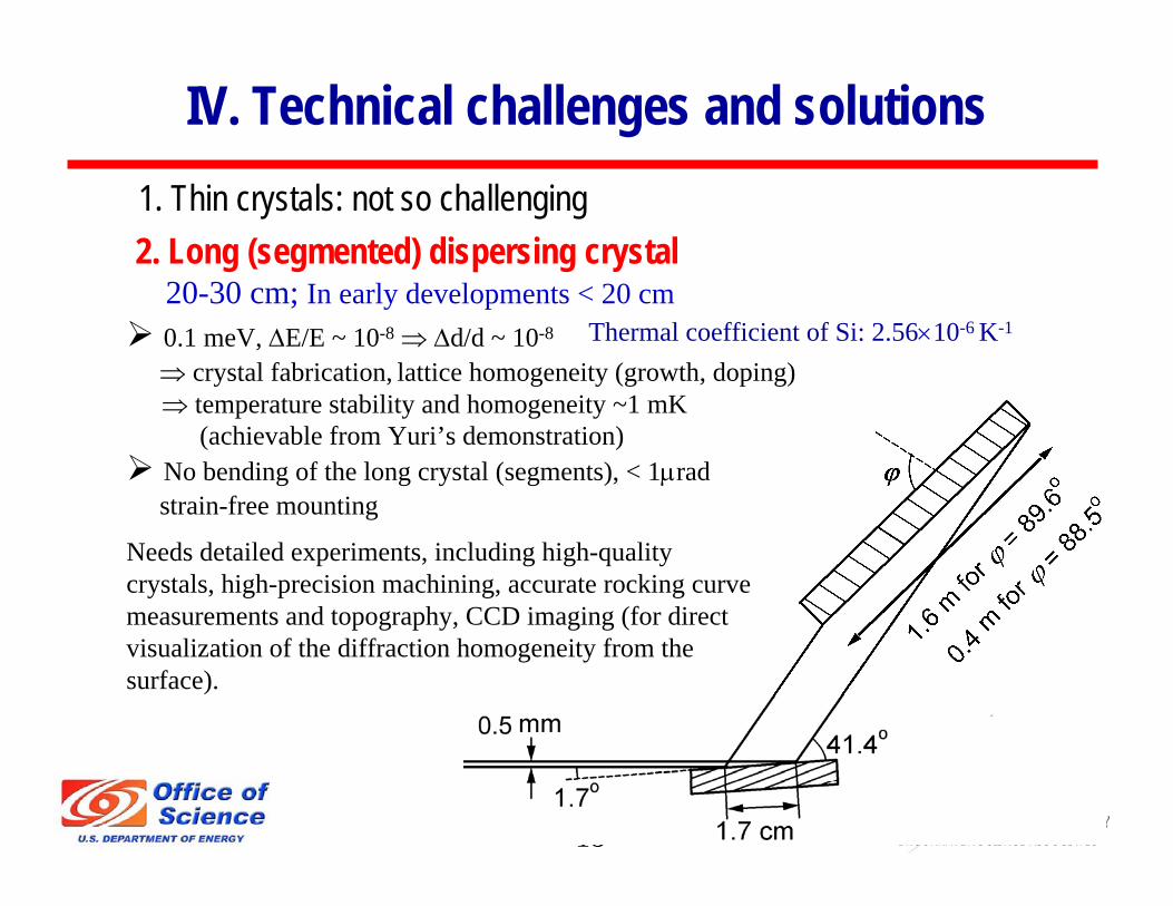
2. Long (segmented) dispersing crystal20-30 cm; In early developments < 20 cm0.1 meV, ΔE/E ~ 10-8 ⇒ Δd/d ~ 10-8
⇒ crystal fabrication, lattice homogeneity (growth, doping)⇒ temperature stability and homogeneity ~1 mK
(achievable from Yuri’s demonstration)
Thermal coefficient of Si: 2.56×10⁻⁶ K-1
No bending of the long crystal (segments), < 1μradstrain-free mounting
Needs detailed experiments, including high-quality crystals, high-precision machining, accurate rocking curve measurements and topography, CCD imaging (for direct visualization of the diffraction homogeneity from the surface).
1. Thin crystals: not so challenging
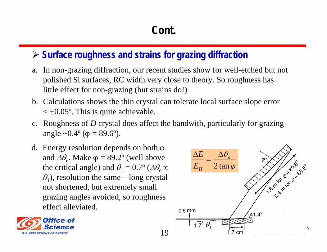
19 BROOKHAVEN SCIENCE ASSOCIATES
θ1
Cont.
Surface roughness and strains for grazing diffraction
2 tane
H
EE
θϕ
ΔΔ=
a. In non-grazing diffraction, our recent studies show for well-etched but not polished Si surfaces, RC width very close to theory. So roughness has little effect for non-grazing (but strains do!)
b. Calculations shows the thin crystal can tolerate local surface slope error < ±0.05º. This is quite achievable.
c. Roughness of D crystal does affect the bandwith, particularly for grazing angle ~0.4º (ϕ = 89.6º).
d. Energy resolution depends on both ϕand Δθe. Make ϕ = 89.2º (well above the critical angle) and θ1 = 0.7º (Δθe ∝θ1), resolution the same—long crystal not shortened, but extremely small grazing angles avoided, so roughness effect alleviated.
20 BROOKHAVEN SCIENCE ASSOCIATES
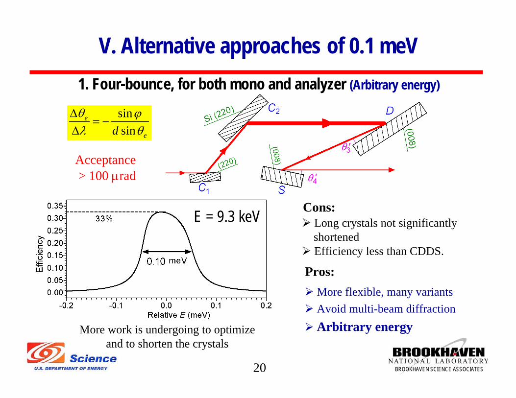
V. Alternative approaches of 0.1 meV
Long crystals not significantlyshortenedEfficiency less than CDDS.
Acceptance> 100 μrad
More flexible, many variants Avoid multi-beam diffractionArbitrary energy
Pros:
Cons:
More work is undergoing to optimize and to shorten the crystals
sinsin
e
edθ ϕλ θ
Δ= −
Δ
E = 9.3 keV
1. Four-bounce, for both mono and analyzer (Arbitrary energy)
21 BROOKHAVEN SCIENCE ASSOCIATES
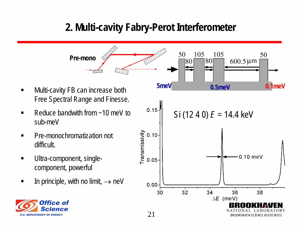
2. Multi-cavity Fabry-Perot Interferometer
Si (12 4 0) E = 14.4 keV
5meV 0.5meV 0.1meVMulti-cavity FB can increase both Free Spectral Range and Finesse.
Reduce bandwith from ~10 meV to sub-meV
Pre-monochromatization not difficult.
Ultra-component, single-component, powerful
In principle, with no limit, → neV
Pre-mono
22 BROOKHAVEN SCIENCE ASSOCIATES
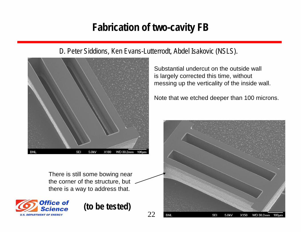
Fabrication of two-cavity FB
Substantial undercut on the outside wallis largely corrected this time, withoutmessing up the verticality of the inside wall.
Note that we etched deeper than 100 microns.
There is still some bowing near the corner of the structure, but there is a way to address that.
D. Peter Siddions, Ken Evans-Lutterrodt, Abdel Isakovic (NSLS).
(to be tested)
23 BROOKHAVEN SCIENCE ASSOCIATES
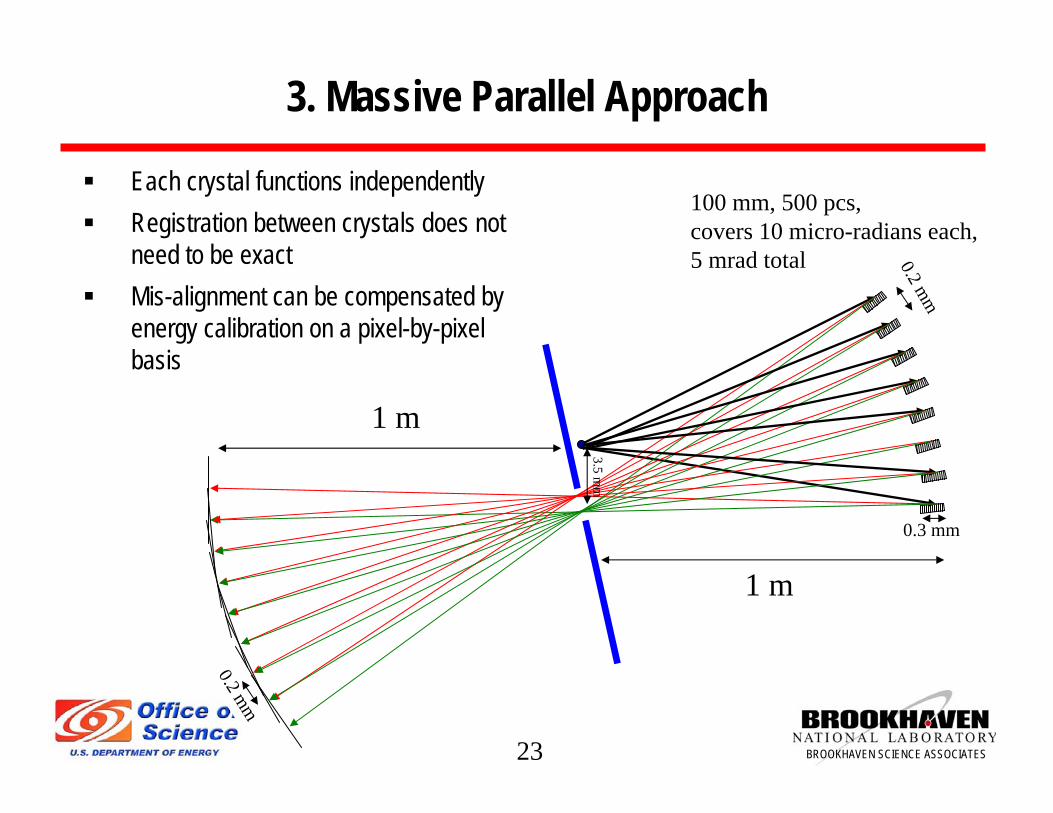
3. Massive Parallel Approach
100 mm, 500 pcs, covers 10 micro-radians each, 5 mrad total
0.2 mm
0.2 mm
1 m
1 m
0.3 mm
3.5 mm
Each crystal functions independentlyRegistration between crystals does not need to be exactMis-alignment can be compensated by energy calibration on a pixel-by-pixel basis
24 BROOKHAVEN SCIENCE ASSOCIATES
VI. 0.1 meV R+D ScheduleFY 07-08 (selected items) — achieve 0.7 meV
Set up all the necessary facilities (monos, slits, detectors, CCD, motors etc) at X15A, NSLSFabricate crystals and repeat Shvyd’ko’s experiment, 0.7 meVSet up temperature-controlled chambers for long dispersing crystals and repeat 0.7 meVTest Bormman effect of and optimize redesigned thin crystals, repeat 0.7 meVCrystal characterization to check crystal quality and its influenceStart testing the inline scheme to achieve 0.3 meV resolution
Dynamical theory calculations of the design (already mature, but to help simulate experiments and optimize designs.)Dynamical theory calculations of alternatives (interferometer, four-bounce, multi-crystal analyzer), concentrating on applicability as analyzer
25 BROOKHAVEN SCIENCE ASSOCIATES
FY 09 — achieve 0.3 meV, move toward 0.1 meV prototype
Full work on the forward inline CDDS mono to achieve 0.3 meV resolution (using the backward CDS analyzer), small-scaleDetailed explore crystal quality (defects, impurities, inhomogeneities) Detailed study of fabrication issues (figure error, roughness) Detailed explore temperature controlIncrease asymmtric angle and elongate crystals for testing 0.1 meV resolution prototype optics (small scale with limited flux)
Determine appropriate focusing and collimating mirrorsTest four-bounce design (small scale with limited flux)Develop and test of Fabry-Perot interferometry and other alternatives undergoing parallel
26 BROOKHAVEN SCIENCE ASSOCIATES
FY10-FY11
FY10Full test of small-scale 0.1 meV optics with limited fluxDesign and test of focusing and collimating mirrorsEngineering design of full-scale 0.1 meV spectrometersDesign and develop engineering solutions for adequate temperature homogeneity and control for full-scale 0.1 meV opticsTest small-scale segmented CDS analyzer
FY11Fabrication of large-scale 0.1 meV spectrometer components, quality testTest large-scale 0.1 meV segmented analyzer (maybe at APS)Test of alternative full-scale multi-crystal analyzer prototypes
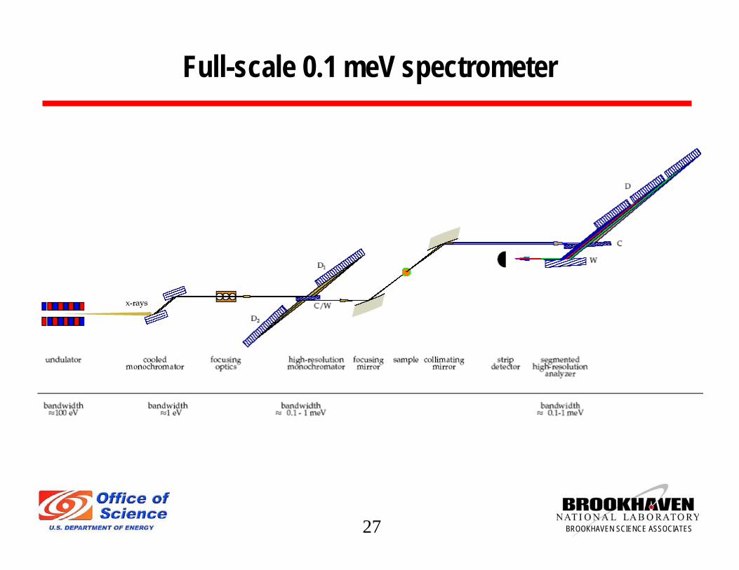
27 BROOKHAVEN SCIENCE ASSOCIATES
Full-scale 0.1 meV spectrometer
28 BROOKHAVEN SCIENCE ASSOCIATES
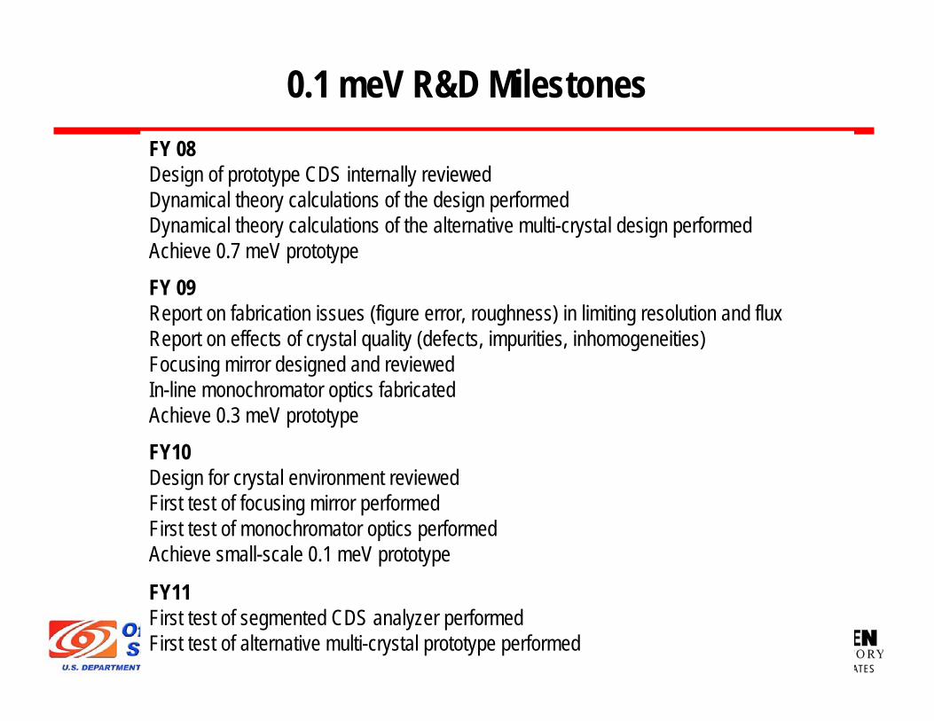
0.1 meV R&D MilestonesFY 08Design of prototype CDS internally reviewed Dynamical theory calculations of the design performedDynamical theory calculations of the alternative multi-crystal design performedAchieve 0.7 meV prototypeFY 09Report on fabrication issues (figure error, roughness) in limiting resolution and fluxReport on effects of crystal quality (defects, impurities, inhomogeneities)Focusing mirror designed and reviewedIn-line monochromator optics fabricatedAchieve 0.3 meV prototypeFY10Design for crystal environment reviewed First test of focusing mirror performedFirst test of monochromator optics performedAchieve small-scale 0.1 meV prototype
FY11First test of segmented CDS analyzer performedFirst test of alternative multi-crystal prototype performed