Embed Size (px)
Citation preview

AT91SAM ARM-based Flash MCU
Application Note
11091A–ATARM–10-Nov-10
Passive InfraRed Reference Design (PIRRD) for SAM3S Motion Detector Camera
1. Scope This application note provides detailed directions and instructions to both hardwareand software engineers building a low cost, yet powerful, Passive InfraRed MotionDetector Camera as found in building or home alarm and monitoring systems. The ref-erence design is based on the SAM3S4C device.
2. Associated Documentation and SoftwareBefore going further into this document, refer to the latest documents for the corre-sponding device and associated tools on the Atmel web site.http://www.Atmel.com/products/at91/sam3s.asp?family_id=605
3. Terminology, Abbreviations and Typographical Conventions
4. KeywordsAtmel ARM® Cortex®-M3, PIR, Passive InfraRed, Camera, SAM3S, CMOS imagesensor, OmniVision®, low-power, IEEE802.15.4, ZigBee®, Wireless....
Abbreviation Description
PIR Passive InfraRed
IR Infra Red
PDC Peripheral DMA controller
ACC Analog Comparator Controller
ACP Analog Comparator
PIO Controller Parallel Input/Output Controller
TWI Two-Wire Interface
GPIO General Purpose Input/Output
BOM Bill of Materials
PSRAM Pseudo Static RAM
SMC Static Memory Controller
FPS Frame Per Second
JTAG Joint Test Action Group

5. OverviewPIR Motion Detectors have been present for a considerable time in building, home alarm andmonitoring systems markets. A PIR Motion Detector predominantly converts a microwave signal,infra-red light in this case, emitted from a human body, for example, into an electrical signal. APIR Motion Detector does not detect a body standing still, but in motion only. For further detailsabout PIR Motion Detection, see Section 10.2 “References”.
Having a PIR Motion Detector on its own is not enough in an alarm or monitoring system. Such asystem is also equipped with a CMOS imaging sensor to take a snapshot of the moving body infront of the PIR sensor. The acquired image can then be transmitted over wired or wirelessmedium.
The reference design implemented around Atmel’s SAM3S Cortex-M3 based MCU is particu-larly well suited for this kind of application and provides ready to use hardware and softwareblocks. The SAM3S PIO Controller integrates an interface able to read data from a CMOS digitalimage sensor and store images in internal or external memory with the CPU being in sleepmode, thus optimizing power consumption when running from batteries. One important require-ment as well, is the image compression process for transmitting images to optimize transmissiontime and in turn, power consumption. Compared to higher priced CMOS imaging sensor deviceswith embedded JPEG compression, the SAM3S device is able to perform JPEG compressionthrough software.
Other features, such as low-power analog comparator or analog-to-digital converter for motiondetection, low-power modes and PIO state preservation (even in backup mode), simplify thedesign by reducing the count of external components, board space and therefore, overall sys-tem cost.
211091A–ATARM–10-Nov-10
Application Note

Application Note
6. Hardware Description
6.1 OverviewHardware choices to reduce BOM, consumption and component count are detailed in the chap-ters that follow.
6.2 PIRRD Board Block DiagramAs shown in the block diagram, the component count is low, thanks to the high integration levelof the SAM3S MCU.
Figure 6-1. PIRRD Block Diagram
AtmelSAM3S4CCortex-M3
320 x 24016-bit ColorTFT display
CMOS SensorOV7740
512KBytesPSRAM
20 pins
Power Supply
+
+
--
IR
PIR
VIR
3V_MCU
3V_DOVDD3V_AVDD
1.5V_DVDD
10-pin connectorATMEL RZ600IEEE 802.15.4
Wireless Module
Power-Down
VDDINVDDIO
ACP+
ACP-
GPIO
SMC
SPI
SMC
JTAG
Debug & DemoPurpose Only
8-bit
GPIO
High LevelLow LevelThreshold
Power-Down
8TWI (I2C)DataClock
Frame/Sync2
Pixel Clock
ButtonGPIO
AmpFilter
USB
5V
3V_MCU
3V_PSRAM
3V LDO
ADVREF
311091A–ATARM–10-Nov-10
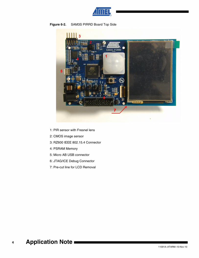
Figure 6-2. SAM3S PIRRD Board Top Side
1: PIR sensor with Fresnel lens
2: CMOS image sensor
3: RZ600 IEEE 802.15.4 Connector
4: PSRAM Memory
5: Micro AB USB connector
6: JTAG/ICE Debug Connector
7: Pre-cut line for LCD Removal
411091A–ATARM–10-Nov-10
Application Note
Application Note
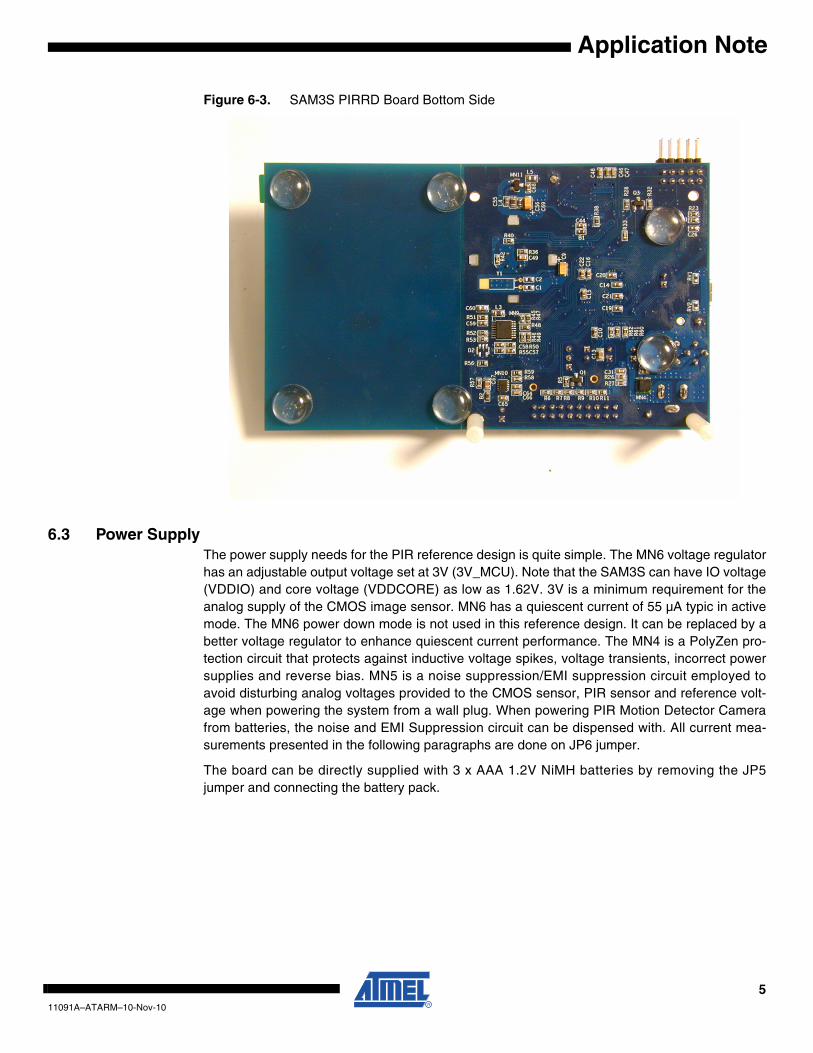
Figure 6-3. SAM3S PIRRD Board Bottom Side
6.3 Power SupplyThe power supply needs for the PIR reference design is quite simple. The MN6 voltage regulatorhas an adjustable output voltage set at 3V (3V_MCU). Note that the SAM3S can have IO voltage(VDDIO) and core voltage (VDDCORE) as low as 1.62V. 3V is a minimum requirement for theanalog supply of the CMOS image sensor. MN6 has a quiescent current of 55 µA typic in activemode. The MN6 power down mode is not used in this reference design. It can be replaced by abetter voltage regulator to enhance quiescent current performance. The MN4 is a PolyZen pro-tection circuit that protects against inductive voltage spikes, voltage transients, incorrect powersupplies and reverse bias. MN5 is a noise suppression/EMI suppression circuit employed toavoid disturbing analog voltages provided to the CMOS sensor, PIR sensor and reference volt-age when powering the system from a wall plug. When powering PIR Motion Detector Camerafrom batteries, the noise and EMI Suppression circuit can be dispensed with. All current mea-surements presented in the following paragraphs are done on JP6 jumper.
The board can be directly supplied with 3 x AAA 1.2V NiMH batteries by removing the JP5jumper and connecting the battery pack.
511091A–ATARM–10-Nov-10

Figure 6-4. Power Supply
6.4 OscillatorsProvisions have been made on the schematics and PCB to use an external slow clock crystaloscillator and 12 MHz crystal for the main oscillator. If no USB or accurate slow clock source isneeded in the application, external crystal oscillators are not needed since the SAM3S embedsone 32.768 kHz RC oscillator and an accurate (factory trimmed) 4/8/12 MHz fast RC oscillator.The internal PLL can work from the fast RC oscillator.
Figure 6-5. Slow Clock and Main Clock Oscillators
DGND
DGND
+3V_MCU+3V
+5VMN5BNX002-01MN5BNX002-01
SV1
SG2
CV3
CG14
CG25
CG36
MN6LP38692MP-ADJMN6LP38692MP-ADJ
VOUT3
EN1
GN
D5
ADJ2
VIN4
JP5JP5
C311uF, X7RC311uF, X7R
R2712K 1%R2712K 1%
C3010uFC3010uF
C28100nFC28100nF
C3210uFC3210uF
+ C2922uF
+ C2922uF
J3MP179P 2.1mmJ3MP179P 2.1mm
12
3
R2616.8K 1%R2616.8K 1%
JP6JP6
MN4ZEN056V130A24LSMN4ZEN056V130A24LS
1
2
3
XIN
XOUT
XOUT32
XIN32
DGND
DGND
C1DNPC1DNP
Y1DNPY1DNP
12
3
C5 15pFC5 15pF
C2DNPC2DNP
C4 15pFC4 15pF
MN1AT91SAM3S-LQFP100MN1AT91SAM3S-LQFP100
PB8_XOUT96
PB9_XIN
PA7_XIN32
PA8_XOUT32
97
7
Y2 12MHzY2 12MHz
611091A–ATARM–10-Nov-10
Application Note
Application Note
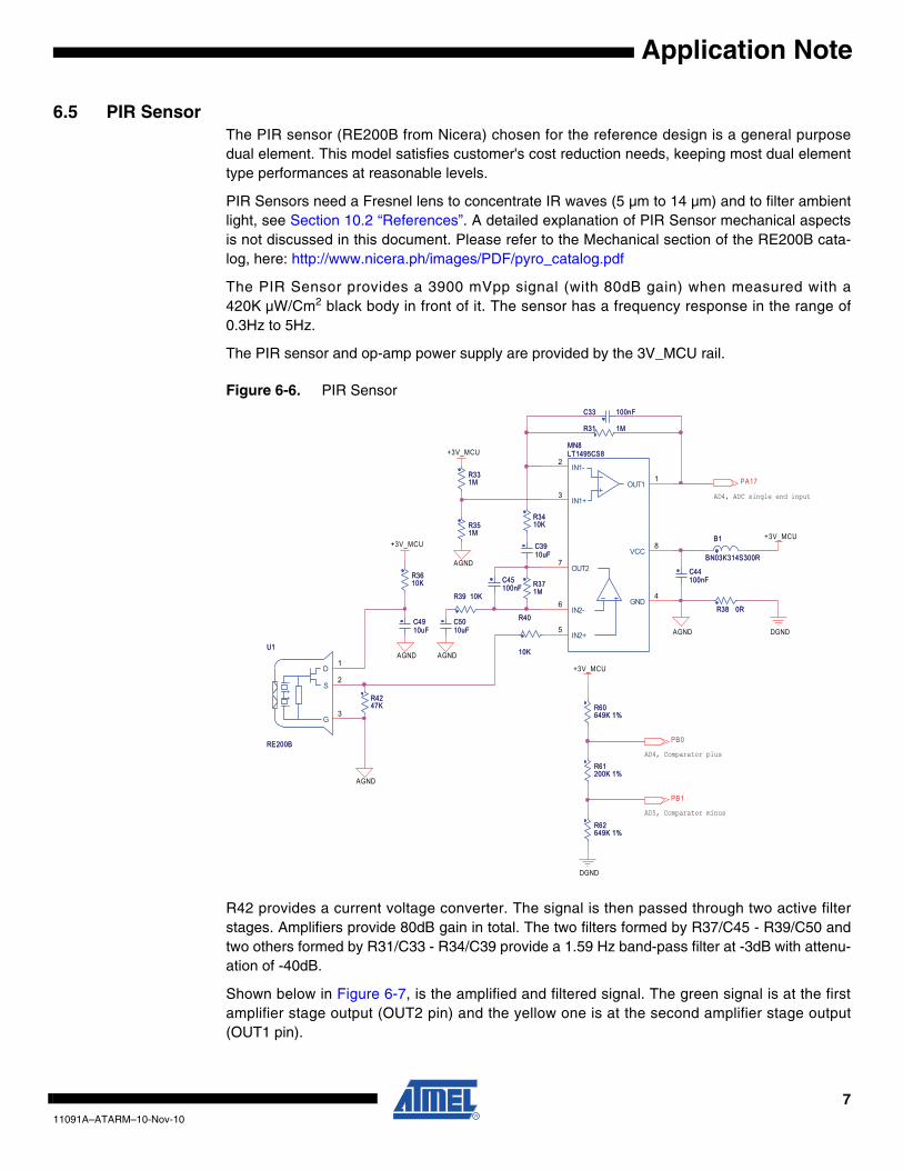
6.5 PIR SensorThe PIR sensor (RE200B from Nicera) chosen for the reference design is a general purposedual element. This model satisfies customer's cost reduction needs, keeping most dual elementtype performances at reasonable levels.
PIR Sensors need a Fresnel lens to concentrate IR waves (5 µm to 14 µm) and to filter ambientlight, see Section 10.2 “References”. A detailed explanation of PIR Sensor mechanical aspectsis not discussed in this document. Please refer to the Mechanical section of the RE200B cata-log, here: http://www.nicera.ph/images/PDF/pyro_catalog.pdf
The PIR Sensor provides a 3900 mVpp signal (with 80dB gain) when measured with a420K µW/Cm2 black body in front of it. The sensor has a frequency response in the range of0.3Hz to 5Hz.
The PIR sensor and op-amp power supply are provided by the 3V_MCU rail.
Figure 6-6. PIR Sensor
R42 provides a current voltage converter. The signal is then passed through two active filterstages. Amplifiers provide 80dB gain in total. The two filters formed by R37/C45 - R39/C50 andtwo others formed by R31/C33 - R34/C39 provide a 1.59 Hz band-pass filter at -3dB with attenu-ation of -40dB.
Shown below in Figure 6-7, is the amplified and filtered signal. The green signal is at the firstamplifier stage output (OUT2 pin) and the yellow one is at the second amplifier stage output(OUT1 pin).
AD4, Comparator plus
AD4, ADC single end input
AD5, Comparator minus
AGND
DGND
AGND AGND
AGND
AGND
+3V_MCU
+3V_MCU
+3V_MCU
+3V_MCU
DGND
PA17
PB0
PB1
C4910uFC4910uF
C44100nFC44100nF
R4247KR4247K
R40
10K
R40
10K
R31 1MR31 1M
R39 10KR39 10KR371MR371M
B1
BN03K314S300R
B1
BN03K314S300RC3910uFC3910uF
C45100nFC45100nF
R61200K 1%R61200K 1%
R3610KR3610K
R351MR351M
R3410KR3410K
R60649K 1%R60649K 1%
C5010uFC5010uF
R331MR331M
R62649K 1%R62649K 1%
MN8LT1495CS8MN8LT1495CS8
IN1-2
IN1+3
OUT27
IN2-6
IN2+5
GND4
VCC8
OUT11
C33 100nFC33 100nF
U1
RE200B
U1
RE200B
D1
S2
G3
R38 0RR38 0R
711091A–ATARM–10-Nov-10

Figure 6-7. Amplified PIR Sensor Output
The “1” pulses represent a premier movement detected in one sense, then “2” pulses indicate asecond motion detected in the opposite sense. The OUT1 signal is then fed to the Analog-to-Digital Converter (ADC) AD0 (PA17) input. Since the ADC and Analog Comparator (ACP) shareanalog inputs, motion detection can be done with the ACP or the ADC. Using the ACP provideslower power consumption whereas using the ADC requires less external components and pro-vides better motion detection sensitivity.
YellowYellow
GreenGreen
811091A–ATARM–10-Nov-10
Application Note
Application Note
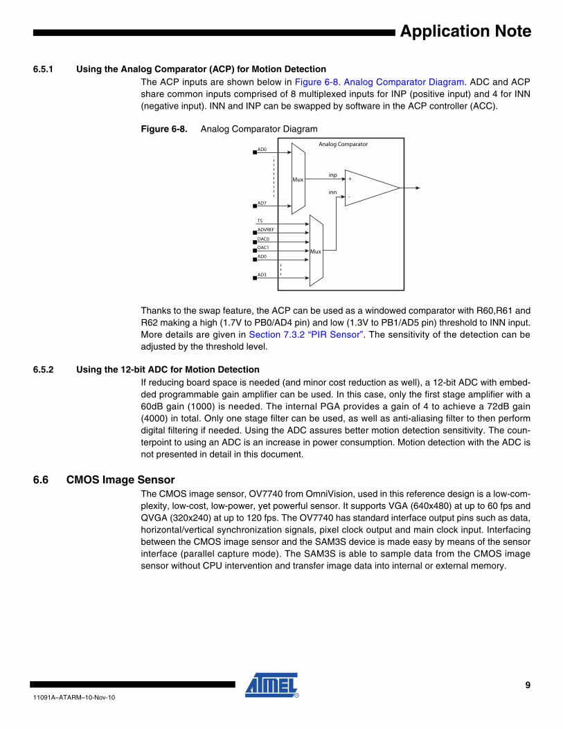
6.5.1 Using the Analog Comparator (ACP) for Motion DetectionThe ACP inputs are shown below in Figure 6-8. Analog Comparator Diagram. ADC and ACPshare common inputs comprised of 8 multiplexed inputs for INP (positive input) and 4 for INN(negative input). INN and INP can be swapped by software in the ACP controller (ACC).
Figure 6-8. Analog Comparator Diagram
Thanks to the swap feature, the ACP can be used as a windowed comparator with R60,R61 andR62 making a high (1.7V to PB0/AD4 pin) and low (1.3V to PB1/AD5 pin) threshold to INN input.More details are given in Section 7.3.2 “PIR Sensor”. The sensitivity of the detection can beadjusted by the threshold level.
6.5.2 Using the 12-bit ADC for Motion DetectionIf reducing board space is needed (and minor cost reduction as well), a 12-bit ADC with embed-ded programmable gain amplifier can be used. In this case, only the first stage amplifier with a60dB gain (1000) is needed. The internal PGA provides a gain of 4 to achieve a 72dB gain(4000) in total. Only one stage filter can be used, as well as anti-aliasing filter to then performdigital filtering if needed. Using the ADC assures better motion detection sensitivity. The coun-terpoint to using an ADC is an increase in power consumption. Motion detection with the ADC isnot presented in detail in this document.
6.6 CMOS Image SensorThe CMOS image sensor, OV7740 from OmniVision, used in this reference design is a low-com-plexity, low-cost, low-power, yet powerful sensor. It supports VGA (640x480) at up to 60 fps andQVGA (320x240) at up to 120 fps. The OV7740 has standard interface output pins such as data,horizontal/vertical synchronization signals, pixel clock output and main clock input. Interfacingbetween the CMOS image sensor and the SAM3S device is made easy by means of the sensorinterface (parallel capture mode). The SAM3S is able to sample data from the CMOS imagesensor without CPU intervention and transfer image data into internal or external memory.
Mux
AD7
AD0
Mux
TS
AD3
ADVREF
DAC0
DAC1
AD0
+
-
inp
inn
Analog Comparator
911091A–ATARM–10-Nov-10

Figure 6-9. OmniVision OV7740 Sensor
As seen in the schematic above, the OV7740 requires three different supplies:
DVDD for digital,
DOVDD for IO,
AVDD for analog
The following supplies are provided.
• Digital (core) rail, DVDD, ranging from 1.70V to 3.5V generated from 3V_OVT
– 1.5V chosen (MN11 regulator) (1.5V internal regulator of OV7740 not used)
• Analog rail, AVDD, ranging from 3.0V to 3.6V generated from 3V_OVT
– 3V chosen
• Input/Output buffer rail, DOVDD, ranging from 3.0V to 3.6V
– 3V chosen
In order to manage power consumption, 3V_OVT is provided from the 3V_MCU rail, controlledby Q3 and SAM3S PC16 pin to switch ON and OFF the CMOS image sensor. The startup timewhen setting PC16 at level one is 0.4ms for MN11. The OV7740 can receive configuration data1ms after its power supplies are stable. Data and command settings are taken into account after5 ms.
The CMOS image sensor is used in 8-bit mode, and gets its clock from a Programmable ClockOutput (PCKO) coming from the SAM3S, which avoids using an external oscillator to provide aclock to the CMOS image sensor. The XVCLK1 (main input clock) ranges from 6 MHz to27 MHz, 24 MHz typical. If using internal SRAM as a memory buffer (32-bit zero wait state mem-ory), the pixel clock from the sensor (PCLK) connected to PIODCCLK (PA23) can be equal to 2times the PIO master clock (PCLK < MCK/2). This is the raw transfer rate of the PIO parallelcapture mode. In the reference design, when taking into account the PSRAM access time of55 ns, PCLK must be inferior or equal to MCK/4 when in color mode and inferior or equal toMCK/3 for black and white mode.
DGND
AGND
AGND
DGND
+3V_OVT+3V_MCU
+3V_OVT
+3V_OVT
DGND
PA21
PA3PA4
PA26PA25PA24
PA28PA27
PA30PA29
PA31
PB13
PC15
PA15PA16PA23
PC16
MN7OV7740MN7OV7740
XVCLK1D5
PWDNA4
RESETBB5
SIOCC4
SIODC5
FSINC2
PCLKE6
HREFC3
VSYNCD1
DATA0E5
DATA1E2
DATA2D4
DATA3D3
DATA4F5
DATA5F2
DATA6E4
DATA7E3
DATA8D2
DATA9E1
DVDDF4
DGNDF3
DOVDDC1
DOVDDC6
DOGNDD6
AVDDA1
AVDDA6
AGNDB1
AGNDB6
VREFHA3
VREFNB2
NC1A2
NC2A5
C36100nFC36100nF
C56100nFC56100nF
C481uFC481uF
R304.7KR304.7K
C371uFC371uF
L4 4.7uHL4 4.7uH
C471uFC471uF
R294.7KR294.7K
L1 4.7uHL1 4.7uH
+
C6910uF
+
C6910uF
R28DNPR28DNP
R64 100KR64 100K
C68
100nF
C68
100nF
C351uFC351uF
C401uFC401uF
C384.7uFC384.7uF
L5 4.7uHL5 4.7uH
R63100KR63100K
C434.7uFC434.7uF
Q3IRLML6401
Q3IRLML6401
1
32
C55100nFC55100nF
R32DNPR32DNP
C411uFC411uF
C341uFC341uF
C42100nFC42100nF
MN11 XC62FP1502MN11 XC62FP1502
VOUT
2
VIN
3
GND
1
L2 4.7uHL2 4.7uH
C461uFC461uF
1011091A–ATARM–10-Nov-10
Application Note
Application Note
Thanks to SAM3S on-die termination (ODT) series resistors, no external ones are needed forclock signals (XVCLK1, PCLK) and data lines. The series resistor helps to reduce I/Os switchingcurrent (di/dt) thereby reducing in turn, EMI. It also decreases overshoot and undershoot (ring-ing) due to inductance of interconnection between devices. ODT helps diminish signal integrityissues and reduce cost and board space.
Configuration of the sensor is done via the Two-Wire Interface (I2C compatible) SIOC (PA4) andSIOD (PA3) pins.
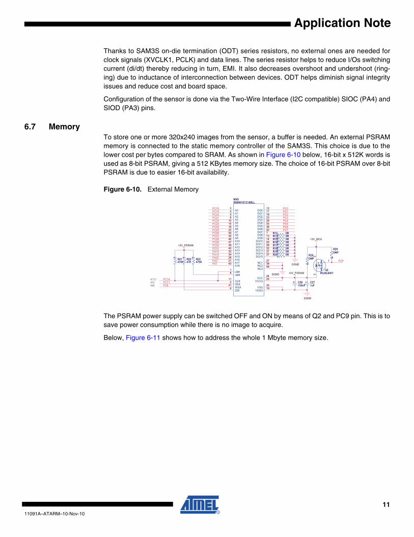
6.7 MemoryTo store one or more 320x240 images from the sensor, a buffer is needed. An external PSRAMmemory is connected to the static memory controller of the SAM3S. This choice is due to thelower cost per bytes compared to SRAM. As shown in Figure 6-10 below, 16-bit x 512K words isused as 8-bit PSRAM, giving a 512 KBytes memory size. The choice of 16-bit PSRAM over 8-bitPSRAM is due to easier 16-bit availability.
Figure 6-10. External Memory
The PSRAM power supply can be switched OFF and ON by means of Q2 and PC9 pin. This is tosave power consumption while there is no image to acquire.
Below, Figure 6-11 shows how to address the whole 1 Mbyte memory size.
NCS0NRDNWE
PC11PC8
PC18 PC0PC1PC2PC3
PC7
PC4
PC6PC5
PC21
PC31
PC20
PC25
PC22
PC19
PA18
PC23
PC27
PC29
PA19
PC24
PC30
PC26
PC28
PA1PA0PA20
PC14
PC9DGND
DGND
DGND
+3V_PSRAM
+3V_MCU
+3V_PSRAM
R18 0RR18 0RR19 0RR19 0R
MN3IS66WV51216BLLMN3IS66WV51216BLL
A03
A14
A25
A39
A410
A515
A616
A722
A844
A945
A1046
A1147
A1239
A1340
A1433
A1534
A1628
A1721
A1843
DQ012
DQ117
DQ218
DQ323
DQ429
DQ535
DQ636
DQ742
DQ87
DQ913
DQ1014
DQ1120
DQ1226
DQ1332
DQ1431
DQ1537
LB#1
UB#8
CE#11
OE#2
WE#41
NC127
NC238
NC348
VCC24
VCCQ25
VSS30
VSSQ19
ZZ#6
R2247KR2247K
R21470KR21470K
R20DNPR20DNP
R13 0RR13 0R
R25DNPR25DNP
C271uFC271uF
R15 0RR15 0R
R12 0RR12 0R
Q2IRLML6401
Q2IRLML6401
1
32R24 0RR24 0R
R23470KR23470K
R16 0RR16 0R
C26100nFC26100nF
R17 0RR17 0R
1111091A–ATARM–10-Nov-10
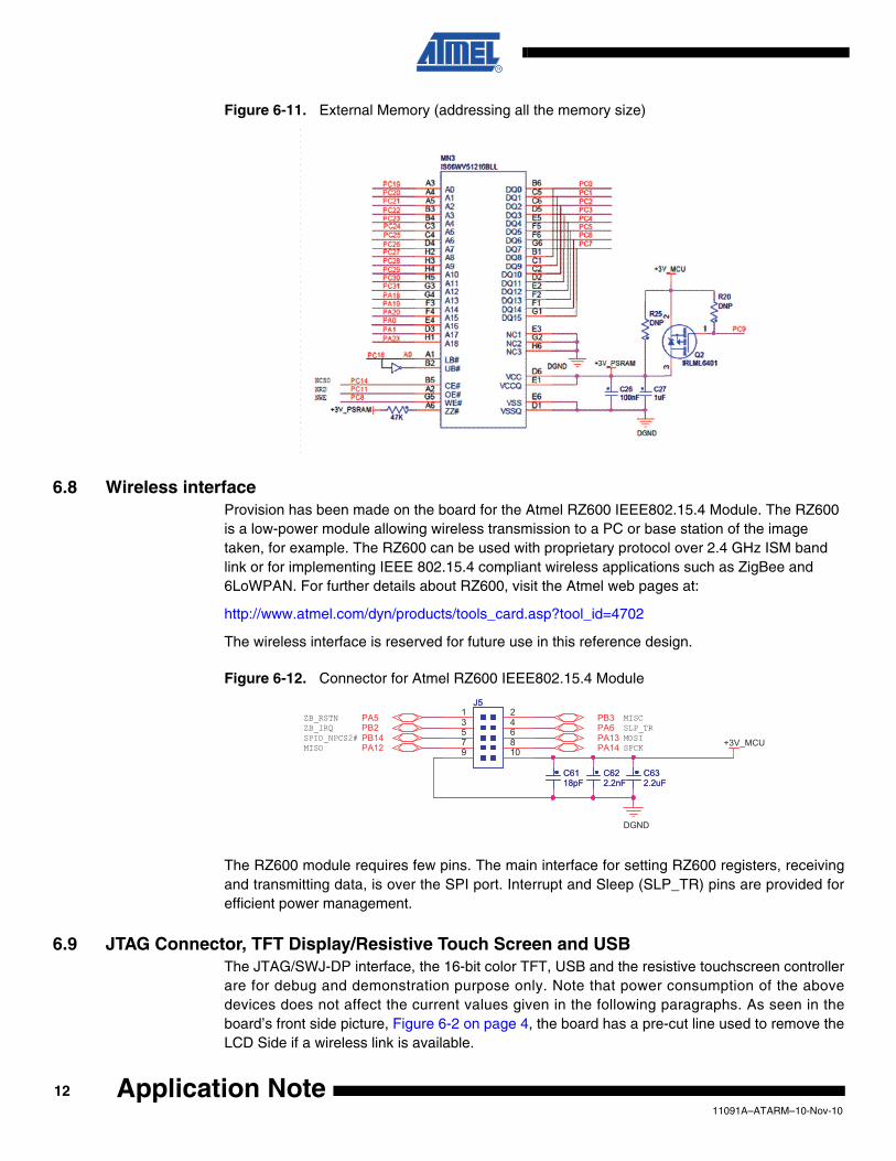
Figure 6-11. External Memory (addressing all the memory size)
6.8 Wireless interfaceProvision has been made on the board for the Atmel RZ600 IEEE802.15.4 Module. The RZ600 is a low-power module allowing wireless transmission to a PC or base station of the image taken, for example. The RZ600 can be used with proprietary protocol over 2.4 GHz ISM band link or for implementing IEEE 802.15.4 compliant wireless applications such as ZigBee and 6LoWPAN. For further details about RZ600, visit the Atmel web pages at:
http://www.atmel.com/dyn/products/tools_card.asp?tool_id=4702
The wireless interface is reserved for future use in this reference design.
Figure 6-12. Connector for Atmel RZ600 IEEE802.15.4 Module
The RZ600 module requires few pins. The main interface for setting RZ600 registers, receivingand transmitting data, is over the SPI port. Interrupt and Sleep (SLP_TR) pins are provided forefficient power management.
6.9 JTAG Connector, TFT Display/Resistive Touch Screen and USBThe JTAG/SWJ-DP interface, the 16-bit color TFT, USB and the resistive touchscreen controllerare for debug and demonstration purpose only. Note that power consumption of the abovedevices does not affect the current values given in the following paragraphs. As seen in theboard’s front side picture, Figure 6-2 on page 4, the board has a pre-cut line used to remove theLCD Side if a wireless link is available.
MISOSPIO_NPCS2# MOSIZB_IRQ
MISCSLP_TR
SPCK
ZB_RSTN
DGND
+3V_MCUPA13
PA5 PB3PA6
PA14
PB2
PA12PB14
C6118pFC6118pF
J5J51 23 45 67 89 10
C622.2nFC622.2nF
C632.2uFC632.2uF
1211091A–ATARM–10-Nov-10
Application Note

Application Note
6.10 General Purpose I/Os ControlThe table below gives a summary of the SAM3S PIOs used to control power supply pins ofexternal devices.
6.11 Reference Design SchematicsSee Section 10. “Appendix”, for schematics and bill of materials details.
6.12 Printed Circuit Board ConsiderationsThe main focus for the PCB layout is around the CMOS image sensor and the PIR sensor (sen-sor + amplifier). No high constraints are required but general rules such as placement ofdecoupling capacitors, power plan distribution, etc., should be followed. As stated in Section 6.6“CMOS Image Sensor”, ODT resistors help reduce PCB design space and assure signal integ-rity to achieve better PIR detection and image quality.
Table 6-1. PIO Control Summary
Device Pin Active Level
CMOS Image Sensor PC16 0
PSRAM PC9 0
1311091A–ATARM–10-Nov-10

7. Software Description
7.1 OverviewThe software is intended to provide some guidance to use with SAM3S and components on thePIRRD board. It can also be used as a reference design to deliver a final product.
The software is composed of three examples and three demos. The three examples providebasic functions for certain peripherals and components on the board. The first example perfomsmotion detection using the PIR sensor. The second one captures an image with the CMOSImage Sensor. The last one performs JPEG compression by software. The three demos providereference designs or demonstrations for specific low-power mode available in SAM3S and func-tion of PIR camera as well, which can help users achieve low power consumption and highperformance balance for final products.
To get the power consumption of the application, it is sequentially split into several phases andpower consumption is measured in each phase as the tables in Section 8. All the measured fig-ures under each phase could be synthesized to get the total power consumption.
All the examples and demos are provided with IAR project files included in the accompaniedsoftware package.
7.2 Demonstration ApplicationsDescribed below are three demonstration applications for the reference design:
• Single Snapshot Mode
• Periodic Wake-up Mode with Motion Detection Mode
• Continuous Capture Mode
These three applications (demos) are provided for use under particular circumstances. Theseapplications integrate several basic functions to accomplish a special task in distinct powermodes.
Further, information is provided on MCU initialization, PIR sensor, CMOS image sensor, JPEGcompression.
7.2.1 Single Snapshot Mode This mode demonstrates CMOS image sensor capture through the SAM3S device backupmode. SAM3S wake-up input pins wake up the system when motion is detected. In this refer-ence design, this is emulated by the on-board push button. This mode is based on the Backupmode as defined in the SAM3S series datasheet.
The current in backup mode can be as low as 21 µA and the wake-up time is around 856 µs. Formore detailed data on power consumption and duration, see the tables in Section 8. “PowerConsumption and Battery Life Time”.
The detailed procedure is provided below in Figure 7-1. Flowchart of Single Snapshot Mode.
1411091A–ATARM–10-Nov-10
Application Note
Application Note
Figure 7-1. Flowchart of Single Snapshot Mode
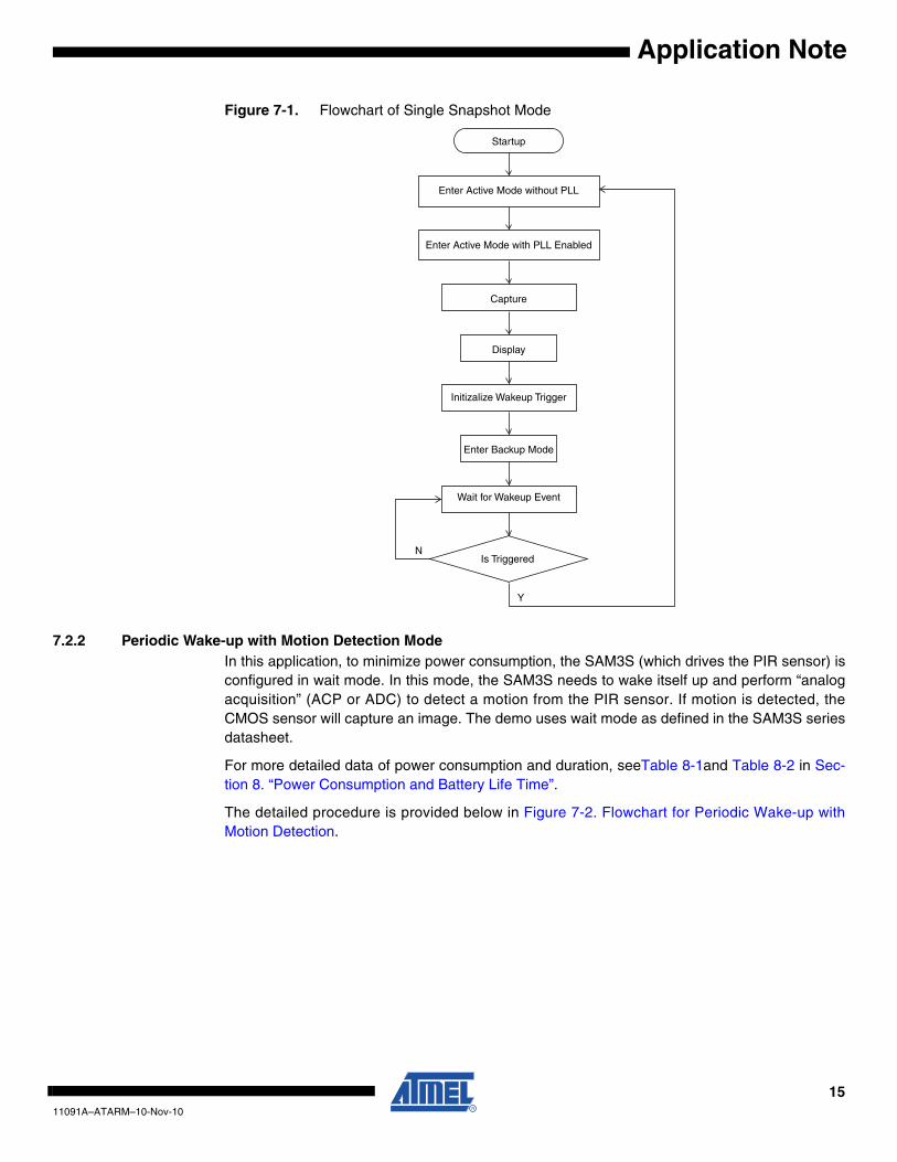
7.2.2 Periodic Wake-up with Motion Detection Mode In this application, to minimize power consumption, the SAM3S (which drives the PIR sensor) isconfigured in wait mode. In this mode, the SAM3S needs to wake itself up and perform “analogacquisition” (ACP or ADC) to detect a motion from the PIR sensor. If motion is detected, theCMOS sensor will capture an image. The demo uses wait mode as defined in the SAM3S seriesdatasheet.
For more detailed data of power consumption and duration, seeTable 8-1and Table 8-2 in Sec-tion 8. “Power Consumption and Battery Life Time”.
The detailed procedure is provided below in Figure 7-2. Flowchart for Periodic Wake-up withMotion Detection.
Enter Active Mode without PLL
Enter Active Mode with PLL Enabled
Initizalize Wakeup Trigger
Is Triggered
Capture
Display
Enter Backup Mode
Wait for Wakeup Event
Startup
N
Y
1511091A–ATARM–10-Nov-10

Figure 7-2. Flowchart for Periodic Wake-up with Motion Detection
Startup
Enter Wait Mode
Initialize M ms RTT Alarm
Initialize Motion Detect and N ms Time-out Interval
Motion Detected or Time-out Interval Expired
Capture
Display
Enter Active Mode with PLL Enabled
Enter Sleep Mode
Is Motion Detected and !(Is Interval Expired)
Y
N
Alarmed
Enter Active Mode without PLL
Enter Active Mode without PLL
1611091A–ATARM–10-Nov-10
Application Note
Application Note
7.2.3 Continuous Capture ModeThis mode is intended to improve frame rate performance when capturing images and displayingthem onto the LCD. Only the frame rate and the total average current are given in this mode.The push button is used to switch between color and B&W mode. B&W mode can achieve betterframe rate performance. More details are given below in Figure 7-3. Flowchart for ContinuousCapture Mode.
Figure 7-3. Flowchart for Continuous Capture Mode
7.3 Code Implementation
7.3.1 MCU InitializationFor demos, it is necessary to perform certain initialization tasks to meet various requirements,such as low-power mode, clock configuration, and initialization of some application-specificcomponents.
7.3.1.1 PIO Configuration for Low-power ModeFor low-power consumption, the external components should be shut down while the system isin backup mode or wait mode. This can be achieved by configuring PIOs high to enable thePMOS cut-off switch. See, Section 6.10 “General Purpose I/Os Control”
To avoid leakage, configure low (with pull-up disabled) unused I/Os connected to pad from inac-tive external devices.
Configure unused I/Os which are connected from pad to active devices, depending on the exter-nal circuit. For example, PC12 connected to LED can be configured as an input with pull-upresistor enabled.
Startup
Initialize Reconfiguration Trigger
Capture
Y
Initialize color mode out_mode as COLOR
Is out_mode changed (B/W or COLOR)
Re-configure PIO parallel capture mode N
Display in out_mode mode
1711091A–ATARM–10-Nov-10

The following code demonstrates setting PC12 as an input with pull-up resistor enabled. All def-initions such as:PIOC, PIO_ODR etc., can be found in the device header file, for example, SAM3S4.h for theSAM3S4 device.
/* Disable the output on PC12 */
PIOC->PIO_ODR = (1<<12);
/* Enable PIO to control PC12 */
PIOC->PIO_PER = (1<<12);
/* Enable the pull up resistor on PC12 */
PIOC->PIO_PUER =(1<<12);
/* Disable the pull down resistor on PC12*/
PIOC->PIO_PPDDR=(1<<12);
7.3.1.2 Clock for Maximum FrequencyThe main clock source is the internal fast RC Oscillator. By default, its frequency is 4 MHz. Tosupport 12 MHz output, the 3-bit MOSCRCF field in PMC Clock Generator Main Oscillator Reg-ister can be set to enable it.
The following code configures the fast RC oscillator at 12 MHz:
/* Enable Fast RC oscillator at 12Mhz.*/
if( (PMC->CKGR_MOR & CKGR_MOR_MOSCRCF) != (0x2 << 4))
{
PMC->CKGR_MOR = (0x37 << 16) | CKGR_MOR_MOSCRCEN|(0x2<<4);
/* Wait the Fast RC to stabilize*/
while ( !(PMC->PMC_SR & PMC_SR_MOSCRCS) ) ;
}
To enable maximum 64 MHz for master clock and processor clock, PLLA is activated. Fordetailed setting, check the accompanying software for reference. A piece of code switching MCKto PLLA with pre-scaler is as follows (timeout is a predefined 32-bit integer variable). Payattention to the sequence of setting MCKR, which differs from case to case. A detailed descrip-tion is in the PMC part of the datasheet:
/* Initialize PLLA */
PMC->CKGR_PLLAR = ((1 << 29) | (0x1f << CKGR_MUL_SHIFT) \
| (0x1 << CKGR_PLLCOUNT_SHIFT) \
| (0x3 << CKGR_DIV_SHIFT));
while (!(PMC->PMC_SR & PMC_SR_LOCKA));
/* set pres */
PMC->PMC_MCKR = (PMC->PMC_MCKR & (uint32_t)~PMC_MCKR_PRES)|PMC_MCKR_PRES_CLK_2;
for ( timeout = 0; !(PMC->PMC_SR & PMC_SR_MCKRDY) && (timeout++ < CLOCK_TIMEOUT) ; );
/* Switch to PLLA*/
1811091A–ATARM–10-Nov-10
Application Note

Application Note
PMC->PMC_MCKR = (PMC->PMC_MCKR & (uint32_t)~PMC_MCKR_CSS)|PMC_MCKR_CSS_PLLA_CLK; ;
for ( timeout = 0; !(PMC->PMC_SR & PMC_SR_MCKRDY) && (timeout++ < CLOCK_TIMEOUT) ; );
7.3.1.3 PSRAM InitializationAs SRAM size (48 Kbytes on SAM3S4 devices) is not sufficient to store memory for capture buf-fer, image frame buffer, etc., PSRAM is applied for memory usage as large as several hundredkilo bytes.
The PSRAM is driven by the SMC (Static Memory Controller), the user interface of which con-tains several registers to configure the timing and mode for PSRAM. See the SAM3S seriesdatasheet for SMC registers bit-field descriptions.
To enable a clock for SMC, the interface below can be called, where ID_SMC is the peripheralidentifier for SMC.
/* Enable peripheral clock */
PMC_EnablePeripheral( ID_SMC ) ;
The SMC in SAM3S has 4 chip selects. The user needs to configure the respective one. Thechip select number can be indexed in the SMC structure defined in the device header file. Forexample,
SMC->SMC_CS_NUMBER[0] is related to chip select 0 which is used for PSRAM on SAM3S-PIRRD.
The full sample code is provided in the package: libboard_sam3s-pirrd library.
7.3.2 PIR SensorThe PIR sensor is accompanied by an Analog Comparator to provide motion detection. A refer-ence voltage is used to determine the sensitivity of the detector.
7.3.2.1 Motion Detection Using the Analog Comparator and PIR SensorThe PIR sensor senses the energy change while a living body moves across its field of view.This change generates voltage deviation from the static output. The deviation varies from caseto case, as determined by the distance from the sensor and the body’s temperature.
The analog comparator compares two input voltages and gives the result. Two signals can beapplied to the inputs of the ACC (analog comparator controller). One is the output of the PIRsensor and the other is a reference voltage provided by a resistor. The reference can beadjusted depending on the need.
7.3.2.2 ACC InitializationFor the ACC implementation in SAM3S devices, the clock should be enabled first through thePMC interface. The two inputs are selected through the ACC mode register. Edge type for com-paring output can be configured too. The sample code of ACC initialization is provided bypyrosensor_motion_detect example.
The chip library contains the interface operating on ACC. The most important one isACC_configure. Its definition follows:
1911091A–ATARM–10-Nov-10

extern void ACC_Configure( Acc *pAcc, uint8_t idAcc, uint8_t ucSelplus, uint8_t ucSelminus,uint16_t wAc_en, uint16_t wEdge, uint16_t wInvert )
where ucSelplus and ucSelminus are the paired inputs and wEdge is the edge type.
7.3.2.3 ACC Comparison Interrupt HandlerThe ACC comparison interrupt is enabled through the ACC Interrupt Enable Register andchecked through the ACC Interrupt Status Register. The flag, SCO (Synchronized ComparatorOutput) in the ACC Interrupt Status Register is used to check the comparison result of twoinputs.
If the comparison edge interrupt is captured, the system falls into ACC_IrqHandler for interrupthandling. In the handler, SCO is checked and the comparison result is updated as well.
7.3.2.4 Software ExampleA PIR Sensor motion detection example is provided in the “examples_pirrd” folder,“pyro_sensor_motion_detect”.
7.3.3 CMOS Imaging SensorThe SAM3S device is capable of capturing parallel data in synchronization with an externalclock, which is used for interfacing to a CMOS image sensor.
7.3.3.1 Initialization of PIO Parallel Capture and OV7740An 8-bit parallel capture mode is available inside the SAM3S PIO controller. It is used to inter-face a CMOS digital image sensor.
OV7740 is a CMOS image sensor with maximum VGA output, RAW RGB and YUV format, I2Ccompatible serial interface. For our application, PIO capture mode is used for the clock and datainterface and TWI (I2C compatible) for serial controlling interface.
For the detailed description of the PIO parallel capture function and settings, refer to the ParallelInput/Output Controller section in the SAM3S series datasheet. Only a few functions are pre-sented here: B&W mode and color mode setting, master clock/pixel clock and capture size.
7.3.3.2 B&W Mode and Color Mode SettingFor the YUV422 output from the sensor, Y is twice the amount than U and V and interleaved withthem. That is, the output is Y: U: Y: V or U: Y: V: Y in sequence. Y is the luminance componentin a color space and the only one for the black and white mode. So it’s adequate for the systemto only have half-sized samples. This can be obtained by setting HALFS to 1 in PIO_PCMR. Thecode below enables or disables half sampling, depending on the output mode:
/* B & W mode*/
if(out_mode == OUT_MONO){
pio->PIO_PCMR &= ~((uint32_t)PIO_PCMR_HALFS);
pio->PIO_PCMR |= PIO_PCMR_HALFS;
pio->PIO_PCMR &= ~((uint32_t)PIO_PCMR_FRSTS);
}else if(out_mode == OUT_COLOR){
/* COLOR mode*/
pio->PIO_PCMR &= ~((uint32_t)PIO_PCMR_HALFS);
}
2011091A–ATARM–10-Nov-10
Application Note

Application Note
7.3.3.3 Master Clock/Pixel ClockThe master clock is provided through the Programmable Clock with multiplexed I/Os. Thesource and pre-scaler are set in PMC Programmable Clock Register. Additionally, the relevantPIO should be configured for working in respective peripheral mode. For example, PB13 can beconfigured as PCK0 in Peripheral B mode.
The source of PCK can be slow clock, main clock and PLL. For flexible clock output from PCK,PLL is a good choice in combination with the prescaler. In SAM3S-PIRRD, OV7740 works in awide range of frequencies from 6 MHz to 27 MHz. To support best capture performance, the PIOparallel capture mode should work at its best capability. In the SAM3S device, the PIO controllerclock frequency must be at least twice the Pixel Clock frequency. That is, the Pixel Clock shouldbe less than half the frequency of 35 MHz (as listed in I/O /Characteristics table in the ElectricalCharacteristics section of the SAM3S series datasheet). For example, in the referenced applica-tion, the frequencies of Master clock and Pixel clock to and from OV7740 are configured to16 MHz, which meets the requirements of both OV7740 and PIO capture mode.
See code below to check how it works.
Pmc *pmc = (Pmc*) PMC;
const PIN pinPCK = {PIO_PB13B_PCK0, PIOB, ID_PIOB, PIO_PERIPH_B, PIO_DEFAULT};
/* configure PB13 working in peripheral B*/
PIO_Configure(&pinPCK,1);
/* PLLA is 128MHz so that PCK0 is 128MHz/8 = 16MHz*/
pmc->PMC_PCK[0] = 0x32;
/* Enable PCK0 output*/
pmc->PMC_SCER = PMC_SCER_PCK0;
while(!( pmc->PMC_SCSR & PMC_SCSR_PCK0));
7.3.3.4 Captured Size The captured size is determined by the size of the captured image and mode, color or B&W. Inconsideration of the word width in a 32-bit machine, it is also affected by the bits in one transfer.The DSIZE bit field in PIO Parallel Capture Mode Register is used for this purpose. For example,if the original size is QVGA and the destination is QVGA in B&W, the captured size should beorg_size/2/4 with DSIZE as 2. The org_size is 240*320*2 representing color data in YUV422 ofQVGA. Being divided by 2 is because B&W is chosen. Being divided by 4 is because the wordwidth is 32 bits.
7.3.3.5 Parallel Capture Event HandlerThe parallel capture event is associated with PDC transfer event. It’s the same as other applica-tions of PDC transfers and used with or without interrupt support.
• With interrupt support: Provides routines for special handling in PIOA_IrqHandler.
• Without interrupt support: Checks PDC flags after transfer size is set and the PDC is enabled as done in image sensor_capture application.
7.3.3.6 Image Quality ImprovementThe Auto White Balance (AWB) and Auto Exposure (AE) settings of the OV7740 image sensorare set to auto mode by default, so the image sensor gets good quality of images under differentenvironments. But this increases the tuning time and needs frames before it can get good imagequality. In the software, because the image sensor is put into low-power mode and wakes up
2111091A–ATARM–10-Nov-10

from time to time, if the AWB and AE are set to auto mode, the first frame’s quality after wake upwill not be perfect.
In order to improve the image quality, the following method is used to improve the image quality.After power up, the AWB and AE of the image sensor are set to auto mode. Before the first cap-ture, the software will wait three seconds for AWB and AE tuning, then the parameters of theAWB and AE settings will be saved in the SAM3S backup registers, and AWB and AE will be setto manual mode. Afterwards, each time before capture, the AWB and AE will be configuredusing these saved (good) parameters from the backup register. Thus after the wake-up, andthanks to the saved parameters, the quality of the first image is improved. Note that this methodwill make the first capture after power up longer, because there is a three-second waiting timefor the good AWB and AE parameters to settle. Also, this method only improves the image qual-ity if the environment does not change greatly compared with the time that AWB and AE performauto tuning.
7.3.3.7 Software ExampleAn image sensor example is provided in the “examples_pirrd” folder, “imagesensor_capture”.See the Section 7.4 “Software Deliveries” on page 24 for more details.
7.3.4 JPEG Compression
7.3.4.1 Introduction to JPEG Compression ExampleThe jpeg_compression example is designed to provide a powerful method to support JPEGcompression from captured YUV data for efficient transfers. An open source code project calledIndependent JPEG Group (IJG) library is ported and integrated into the example to accomplishthe task. After capture and compression, the data for compression time, decompression time,compression ratio, memory and LCD accessing speed would be provided to show theperformance.
7.3.4.2 IJG JPEG Compression LibraryIJG writes and distributes a widely used free library for JPEG image compression. Compressionand decompression library, example code and documents are provided in the software packagefrom IJG.
In order to encode an image into JPEG, the following functions are used:
JpegData_SetSource(): Source buffer pointer and length, which points to the starting of the buffer that is going to be compressed.
JpegData_SetDestination(): Destination buffer pointer and length, which points to the starting of the buffer that is going to store the results.
JpegData_SetDimensions(): Set Image dimensions
JpegData_SetParameters(): To set image quality, input format and compression method
ijg_compress(): Start JPEG encoding
In order to decode JPEG, the following functions are used:
JpegData_SetSource(): Source buffer pointer and length, which points to the starting of the buffer that is going to be decompressed.
JpegData_SetDestination(): Destination buffer pointer and length, which points to the starting of the buffer that is going to store the results.
JpegData_SetDimensions(): Set Image dimensions
2211091A–ATARM–10-Nov-10
Application Note

Application Note
JpegData_SetParameters(): To set image quality, input format and compression method
ijg_decompress(): Start JPEG decoding
Note that IJG library supports compression with the input formats, YUV420 or YUV444. Sincethe image sensor’s output is YUV422, a conversion from YUV422 to YUV444 is needed beforeusing the IJG library without first changing the library.
Once the library has been changed (by Atmel) to support YUV422, it is supported in the deliv-ered software, so conversion of YUV422 to YUV444 is not necessary.
IJG library supports several compression/decompression methods, among which are IFAST andISLOW. IFAST is faster, but a less accurate method. ISLOW is slower, but a more accuratemethod. The user can choose between these methods accordingly. For detailed informationabout IJG library, refer to their web site http://www.ijg.org/.
7.3.4.3 JPEG Compression and its PerformanceThe jpeg_compression example provides a seamless interface for YUV422 data compressionfrom the image sensor and storing the JPEG file to PSRAM. The dynamic memory for compres-sion objects is located in SRAM to achieve better total performance. The default matrix for busaccess to memory is optimized for better performance. The sample code is found in the softwarepackage.
Putting the dynamic memory for compression in PSRAM can also be done from software, whichoffers users another option when the SRAM is not sufficient in their application. Note that a dif-ferent scatter file should be used. For details, refer to “jpeg_compression” examples containedin “source_pirrd_1.0.zip”. See, Section 7. “Software Description”.
Note that all the performance data is measured under on-board 55 ns PSRAM with the proces-sor clock at 64 MHz.
Performance data is as follows:
Note that in software, the JPEG compression uses the captured image from the OV7740, so theperformance data can vary due to the environment for capture changing.
Table 7-1. JPEG Compression/Decompression Performance
Compress Decompress
Heap in SRAM 218 ms 181 ms
Heap in PSRAM 317 ms 398 ms
Table 7-2. JPEG Memory Consumption
Flash (Bytes) SRAM (Bytes) PSRAM (Bytes)
Heap in SRAM 81,892 (RO)47,094
(RW+Stack+Heap)
168,960
(Buffer)
Heap in PSRAM 81,892 (RO)5,112
(RW+Stack)
210944
(Buffer+Heap)
2311091A–ATARM–10-Nov-10

7.3.4.4 Using the JPEG LibraryA JPEG compression example is provided in the “examples_pirrd” folder, “jpeg_compression”that shows how to use the JPEG library. See Section 7.4 “Software Deliveries” on page 24 formore details.
7.4 Software Deliveries
7.4.1 Contents OverviewThe SAM3S-PIRRD software package consists of binaries and source code of 3 basic examplesand 3 demos. Files provided with this user application note are:
• bin_pirrd_1.0.zip: Binary Files
• ewarm_pirrd_patch.zip: IAR EWARM 5.50 Patch.
• source_pirrd_1.0.zip: Source code files of the demos and examples
The examples provide basic function of related peripherals, such as motion detection, imagesensor capture and JPEG compression.
The demos provide reference designs or demonstrations used in SAM3S low-power mode. Sev-eral peripherals are involved to complete a special demo, for example, the system is periodicallywoke up from wait mode and takes pictures as long as motion is detected.
Examples:
• imagesensor_capture
• jpeg_compression
• pyrosensor_motion_detect
Demos:
• Continuous_Capture_Mode
• Periodic_Motion_Detect_Mode
• Single_Snapshot_Mode
7.4.2 Using the Source CodeTo use the source code for debugging or modification, unzip “source” archive. The directorystructure is as follows (only folders are shown here):
-demo_pirrd
|-Continuous_Capture_Mode
|-Periodic_Motion_Detect_Mode
|-Single_Snapshot_Mode
-examples_pirrd
|-imagesensor_capture
|-jpeg_compression
|-pyrosensor_motion_detect
-libraries
|-libboard_sam3s-pirrd
2411091A–ATARM–10-Nov-10
Application Note

Application Note
|-libchip_sam3s
|-libjpeg
|-memories
|-usb
Before opening the IAR project, patch IAR tools for SAM3S device support, if missing. Therelated archive is ewarm_pirrd_patch.zip.
Each example and demo is provided with an IAR project file, found in “build\ewarm_550” undereach example or demo folder. For example, to see the code for Single_Snapshot_Mode in IAREWARM, go to : “S ing le_Snapsho t_Mode \bu i ld \ewarm_550” then open“single_snapshot_mode.eww”.
The supported version of IAR is 5.50.
7.4.3 Compiling OptionsThe following macros need to be customized for different purposes, especially for demos suchas Single Snapshot Mode and Periodic Wake-up with Motion Detection Mode. These definitionsare found at the very beginning of the “local definition” part of the main.c file.
/*LCD displaying and debugging support*/
#define LCD_DEBUG_OUT
/*State of each phase for current measurement*/
#define STATE_STAYED
/*Enable measuring the average current for reenterable code*/
#define DEBUG_CUR_CAPTURE
If LCD displaying or debugging is necessary, LCD_DEBUG_OUT should be enabled.
If time or power consumption measurement is needed for the application, STATE_STAYED shouldbe enabled.
To get the average current during capture, DEBUG_CUR_CAPTURE should be enabled.
For example, to simply see the regular routine of the application and pictures displayed on theLCD, enable LCD_DEBUG_OUT and comment or remove the other two.
7.4.4 Debug/Release OptionsFor the three demos and jpeg_compression example, there are two options: “Debug” and“Release”.
• “Debug” is for users to debug conveniently, with low optimization, and debug easily step by step.
• “Release” is for better performance, so it is configured as high optimization (Balanced optimization between Speed and Size).
For the other 2 examples, there are 2 release targets “flash” and “sram”. Clearly, the names indi-cate that the user can run the application in the selected memory.
2511091A–ATARM–10-Nov-10

8. Power Consumption and Battery Life Time
8.1 Single Snapshot ModeTable 8-1 below gives current consumption values versus duration of each main software taskrelated to the flow chart shown in Figure 7-1 on page 15. JP6 is used for current measurements.
If, for example, 100 pictures are taken in one day, then the average charge (Amp-Hour) is21E-06 + ((7.73E-03x100)/(24x3600)) = 30 µA.
With 2800 mAh capacitance on a 3V minimum battery supply, a battery life time of 93000 Hoursis furnished, thus around 10 years of run time.
Table 8-1. Power Consumption in Single Snapshot Mode
FunctionDuration
(ms)Active Current
(mA)Charge
(Current*Time) Comments
MCU Wake-up and Initialization
0.856 2.1 1.8E-06
MCK = RC Osc @ 4 MHz
Peripherals: PIOA
Components: PIR
Switch MCK to PLL 0.237 33.4 8E-06
MCK = 64 MHz from PLLA
Peripherals: PIOAComponents: PIR
SAM3S Active (transfer setup)
23.6 58.3 1.4E-03MCK = 64 MHz from PLLAPeripherals: PIOA, SMC, TWI
Components: PIR, PSRAM, Image Sensor
CMOS image sensor
(Transfer into PSRAM) + Core in Sleep Mode
127 49.6 6.3E-03
MCK = 64 MHz from PLLA
Peripherals: PIOA, SMC, TWI
Components: PIR, PSRAM, Image
SAM3S in Backup Mode
– 0.021 –
MCK: stopped
Peripherals: NONEComponents: PIR
TOTAL 7.73E-03
2611091A–ATARM–10-Nov-10
Application Note

Application Note
8.2 Periodic Wake-Up with Motion Detection ModeTable 8-2 below gives current consumption number versus duration of each main software tasksrelated to the flowchart from Figure 7-2 on page 16. JP6 is used for current measurements.
Note: 1. Current during capturing is measured by enabling macro DEBUG_CUR_CAPTURE.
If, for example, 100 pictures are taken in one day, then the average charge (Amp-Hour) is 33E-06 + ((10.6E-03x100) / (24x3600)) = 45.33µA.
With 2800 mAh capacitance on a 3V minimum battery supply, a battery life time of 62000 Hoursis furnished, thus around 7 years of run time.
8.3 Continuous Capture ModeDetails about current consumption for each software task are not given here for this mode. Thisapplication demonstrates the capability of the SAM3S to perform “live video capture”. In blackand white mode the frame rate is 7fps and 5fps in color mode. Source code for this mode is pro-vided in the software package.
Table 8-2. Power Consumption in Periodic Wake-up with Motion Detection Mode
FunctionDuration
(mS)Active Current
(mA)Charge
(Current*Time) Comments
MCU Wake-up from Wait mode and Initialization
0.165 2.234 0.36E-06MCK = RC Osc @ 4MHz Peripherals: ACC, RTT
Components: PIR, LED
Sleep Mode with PIR, ACC and TC
Fixed maximal: 2s
(for test)1.820 3.64E-03
MCK = RC Osc @ 4MHz
Core in sleep
Peripherals: ACC, RTT, TCComponents: PIR, LED
Wake-up from sleep mode
0.030 2.260 0.06E-06MCK = RC Osc @4MHz Peripherals: RTT
Components: PIR, LED
Switch MCK to PLL 0.220 35.29 7.7E-06
MCK = 64 MHz from PLLA
Peripherals: RTT, LED
Components: PIR
SAM3S Active (transfer setup)
20.3 59 1.20E-03
MCK = 64 MHz from PLLA
Peripherals: RTT, LEDComponents: PIR, PSRAM, Image Sensor
CMOS image sensor (Transfer into PSRAM) + Core in Sleep Mode
117 49.25(1) 5.76E-03MCK = 64 MHz from PLLAPeripherals: RTT, LED
Components: PIR, PSRAM, Image Sensor
SAM3S in Wait Mode-
33uA -
MCK stopped
Peripherals: RTT
Components: PIR, LED
TOTAL 10.6E-03
2711091A–ATARM–10-Nov-10

9. Using the Reference Design BoardA 5V DC power supply is needed to power the board (same as provided on the SAM3S-EK).
The default application programmed on the board is the periodic wake-up with motion detectiondemo. After power up, the screen will be black, moving in front of the board causes a picture tobe taken which is displayed on the LCD. Then, each time a movement is detected, the blue LEDwill turn on quickly, a picture is taken and displayed.
If the Single Snapshot Demo is programmed into the board, after power-up, pressing the BP1push button will take a picture.
If the Continuous Capture Mode is programmed into the board, the board acts as a video cam-era. Pushing BP1 button will switch between B&W and color mode.
9.1 Downloading and Running the BinariesTo use the binaries, unzip “bin_pirrd.zip”. The directory structure is as follows:
-demos
|-Continuous_Capture_Mode_Rel.bin
|-Periodic_Motion_Detect_Mode_Rel.bin
|-Single_Snapshot_Mode_Rel.bin
-examples
|-imagesensor_capture_flash.bin
|-jpeg_compression_rel.bin
|-pyrosensor_motion_detect_flash.bin
The binary files can be downloaded directly into the Flash memory using SAM-BA® v2.10 eitherwith Atmel SAM-ICE or via USB port. On Windows® Vista® computer, SAM-BA v2.10 CDC ver-sion must be used for USB port.
Start SAM-BA
Choose the connection and the SAM3S4-EK board, and click Connect.
On the next window shown below, from the Scripts drop-down list choose:
• Enable Flash access script, click “Execute”
• Then Boot from Flash (GPNVM1) script, click “Execute”
• Then click the icon folder close to the “Send File” button, and browse to the desired binary file. “Click Send” File button
• When asked “Do you want to lock the involved region...” choose No
• Close SAM-BA and power down then power up the board. The new application starts.
2811091A–ATARM–10-Nov-10
Application Note
Application Note
The same procedure can be done using the SAM-ICE JTAG/ICE box. Choose jlink\ARM0 con-nection instead.
2911091A–ATARM–10-Nov-10

10. Appendix
10.1 Hardware filesBoard design files are provided with the reference design. See the “Hardware” folder.
Board design and board manufacturing files are provided:
Board Design files:
• SAM3S-PIRRD_RevB.pdf: Schematics, PDF format
• SAM3S-PIRRD_REVB.DSN: Schematics, Cadence® OrCAD® Capture format
• SAM3S-PIRRD_REVB.brd: PCB project, Allegro PCB Design
• SAM3S-PIRRD_REVB.xls: Bill of Materials
Board manufacturing files:
• GERBER files format.
10.2 ReferencesPassive InfraRed Sensors at: http://en.wikipedia.org/wiki/Passive_infrared_sensor.
SAM3S Full datasheet at: http://www.Atmel.com/products/at91/sam3s.asp?family_id=605.
AT91 In-system Programmer (SAM-BA) open set of tools, complete software and support docu-mentation at: http://www.atmel.com/dyn/products/tools_card.asp?tool_id=3883.
3011091A–ATARM–10-Nov-10
Application Note

Application Note
Revision History
Doc. Rev CommentsChange Request Ref.
11091A First issue
3111091A–ATARM–10-Nov-10

Headquarters International
Atmel Corporation2325 Orchard ParkwaySan Jose, CA 95131USATel: 1(408) 441-0311Fax: 1(408) 487-2600
Atmel AsiaUnit 1-5 & 16, 19/FBEA Tower, Millennium City 5418 Kwun Tong RoadKwun Tong, KowloonHong KongTel: (852) 2245-6100Fax: (852) 2722-1369
Atmel EuropeLe Krebs8, Rue Jean-Pierre TimbaudBP 30978054 Saint-Quentin-en-Yvelines CedexFranceTel: (33) 1-30-60-70-00 Fax: (33) 1-30-60-71-11
Atmel Japan9F, Tonetsu Shinkawa Bldg.1-24-8 ShinkawaChuo-ku, Tokyo 104-0033JapanTel: (81) 3-3523-3551Fax: (81) 3-3523-7581
Product Contact
Web Sitewww.atmel.comwww.atmel.com/AT91SAM www.atmel.com/Iproducts/ASIC
Technical SupportAT91SAM SupportAtmel techincal support
Sales Contactswww.atmel.com/contacts/
Literature Requestswww.atmel.com/literature
Disclaimer: The information in this document is provided in connection with Atmel products. No license, express or implied, by estoppel or otherwise, to anyintellectual property right is granted by this document or in connection with the sale of Atmel products. EXCEPT AS SET FORTH IN ATMEL’S TERMS AND CONDI-TIONS OF SALE LOCATED ON ATMEL’S WEB SITE, ATMEL ASSUMES NO LIABILITY WHATSOEVER AND DISCLAIMS ANY EXPRESS, IMPLIED OR STATUTORYWARRANTY RELATING TO ITS PRODUCTS INCLUDING, BUT NOT LIMITED TO, THE IMPLIED WARRANTY OF MERCHANTABILITY, FITNESS FOR A PARTICULARPURPOSE, OR NON-INFRINGEMENT. IN NO EVENT SHALL ATMEL BE LIABLE FOR ANY DIRECT, INDIRECT, CONSEQUENTIAL, PUNITIVE, SPECIAL OR INCIDEN-TAL DAMAGES (INCLUDING, WITHOUT LIMITATION, DAMAGES FOR LOSS OF PROFITS, BUSINESS INTERRUPTION, OR LOSS OF INFORMATION) ARISING OUTOF THE USE OR INABILITY TO USE THIS DOCUMENT, EVEN IF ATMEL HAS BEEN ADVISED OF THE POSSIBILITY OF SUCH DAMAGES. Atmel makes norepresentations or warranties with respect to the accuracy or completeness of the contents of this document and reserves the right to make changes to specificationsand product descriptions at any time without notice. Atmel does not make any commitment to update the information contained herein. Unless specifically providedotherwise, Atmel products are not suitable for, and shall not be used in, automotive applications. Atmel’s products are not intended, authorized, or warranted for useas components in applications intended to support or sustain life.
© 2010 Atmel Corporation. All rights reserved. Atmel®, Atmel logo and combinations thereof, SAM-BA® and others are registered trademarksor trademarks of Atmel Corporation or its subsidiaries. ARM®, and the ARMPowered® logo and others are registered trademarks or trademarksARM Ltd. Windows® and others are registered trademarks or trademarks of Microsoft Corporation in the US and/or other countries. Other termsand product names may be trademarks of others.
11091A–ATARM–10-Nov-10