Embed Size (px)
Citation preview

Passive Circuit DesignGuide
August 2005

Notice
The information contained in this document is subject to change without notice.
Agilent Technologies makes no warranty of any kind with regard to this material,including, but not limited to, the implied warranties of merchantability and fitnessfor a particular purpose. Agilent Technologies shall not be liable for errors containedherein or for incidental or consequential damages in connection with the furnishing,performance, or use of this material.
Warranty
A copy of the specific warranty terms that apply to this software product is availableupon request from your Agilent Technologies representative.
Restricted Rights Legend
Use, duplication or disclosure by the U. S. Government is subject to restrictions as setforth in subparagraph (c) (1) (ii) of the Rights in Technical Data and ComputerSoftware clause at DFARS 252.227-7013 for DoD agencies, and subparagraphs (c) (1)and (c) (2) of the Commercial Computer Software Restricted Rights clause at FAR52.227-19 for other agencies.
© Agilent Technologies, Inc. 1983-2005395 Page Mill Road, Palo Alto, CA 94304 U.S.A.
Acknowledgments
Mentor Graphics is a trademark of Mentor Graphics Corporation in the U.S. andother countries.
Microsoft®, Windows®, MS Windows®, Windows NT®, and MS-DOS® are U.S.registered trademarks of Microsoft Corporation.
Pentium® is a U.S. registered trademark of Intel Corporation.
PostScript® and Acrobat® are trademarks of Adobe Systems Incorporated.
UNIX® is a registered trademark of the Open Group.
Java™ is a U.S. trademark of Sun Microsystems, Inc.
SystemC® is a registered trademark of Open SystemC Initiative, Inc. in the UnitedStates and other countries and is used with permission.
ii
Contents1 Introducing the Passive Circuit DesignGuide
Getting Started ......................................................................................................... 1-1Display Preferences............................................................................................ 1-1Passive Circuit Design Flow ............................................................................... 1-2SmartComponents ............................................................................................. 1-3Automated Assistants......................................................................................... 1-5Accessing the DesignGuide ............................................................................... 1-6The Passive Circuit DesignGuide Control Window............................................. 1-9SmartComponent Palette Access ...................................................................... 1-10
Using the Passive Circuit DesignGuide .................................................................... 1-11Create a New Design ......................................................................................... 1-11Open the DesignGuide Control Window............................................................. 1-11Auto-Design a Microstrip Line Component......................................................... 1-12Design and Analyze a Branch-Line Coupler....................................................... 1-13Optimize the Branch-Line Coupler ..................................................................... 1-14Display Branch-Line Coupler Analysis Results .................................................. 1-15
2 Using SmartComponentsOverview................................................................................................................... 2-1Placing SmartComponents....................................................................................... 2-2Copying SmartComponents ..................................................................................... 2-2
Copying Within A Design.................................................................................... 2-2Copying Between Designs or Schematic Windows............................................ 2-3
Editing SmartComponents ....................................................................................... 2-3Position and Orientation ..................................................................................... 2-3Parameters ......................................................................................................... 2-4
Deleting SmartComponents ..................................................................................... 2-4Delete From Current Design............................................................................... 2-4Delete From Current Project............................................................................... 2-4Delete Manually Using File System.................................................................... 2-4
Design, Analysis, Optimization and Layout .............................................................. 2-5Stand-Alone SmartComponent Usage ..................................................................... 2-5
Using an Existing SmartComponent Within the Same Project........................... 2-6Using an Existing SmartComponent in Any Project ........................................... 2-6
3 Using Automated AssistantsDesign Assistant....................................................................................................... 3-1
Single Component Design.................................................................................. 3-1Multiple Component Design ............................................................................... 3-1
Simulation Assistant ................................................................................................. 3-2
iii
Simulation Frequency Sweep............................................................................. 3-2Automatically Display Results............................................................................. 3-3To Simulate a SmartComponent ........................................................................ 3-3Using Simulation Templates ............................................................................... 3-3
Optimization Assistant .............................................................................................. 3-4To Optimize a SmartComponent ........................................................................ 3-4Optimization Templates ...................................................................................... 3-4
Display Assistant ...................................................................................................... 3-5Display Templates .............................................................................................. 3-5Basic Layout ....................................................................................................... 3-6Typical Area 1 Content ....................................................................................... 3-7Typical Area 2 Content ....................................................................................... 3-8Typical Area 3 Content ....................................................................................... 3-8To Display SmartComponent Performance Results ........................................... 3-9
Layout Generation .................................................................................................... 3-9Creating Layout Artwork ..................................................................................... 3-10Updating Layout Artwork .................................................................................... 3-10
4 SmartComponent ReferenceSmartComponent List............................................................................................... 4-1Passive Circuit DG - Lines........................................................................................ 4-4
MBend (Microstrip Bend Component) ................................................................ 4-4MBStub (Microstrip Butterfly Radial Stub).......................................................... 4-5MCFil (Microstrip Coupled-Line Filter Element) ................................................. 4-7MCLine (Microstrip Coupled Line Component) .................................................. 4-8MCorn (Microstrip Corner Component) .............................................................. 4-9MCross (Microstrip Cross Component) .............................................................. 4-10MCurve (Microstrip Curve Component).............................................................. 4-11MGap (Microstrip Gap Component) ................................................................... 4-12MLine (Microstrip Line)....................................................................................... 4-13MMndr (Microstrip Meander Line) ...................................................................... 4-14MRStub (Microstrip Radial Stub)........................................................................ 4-16MStep (Microstrip Step Component) .................................................................. 4-18MStub (Microstrip Stub)...................................................................................... 4-19MTaper (Microstrip Taper Component) ............................................................... 4-20MTee (Microstrip Tee Component) ..................................................................... 4-21
Passive Circuit DG - RLC ......................................................................................... 4-22MICapP (Microstrip 4-port Interdigital Capacitor) ............................................... 4-22MICapPG (Microstrip Grounded 2-port Interdigital Capacitor) ........................... 4-25MICapS (Microstrip 2-port Interdigital Capacitor) ............................................... 4-28MICapSG (Microstrip 1-port Interdigital Capacitor) ............................................ 4-31MREInd (Microstrip Elevated Rectangular Inductor) .......................................... 4-34
iv
MRInd (Microstrip Rectangular Inductor) ........................................................... 4-37MSInd (Microstrip Spiral Inductor) ...................................................................... 4-40MTFC (Microstrip Thin Film Capacitor) .............................................................. 4-42TFC (Thin Film Capacitor) .................................................................................. 4-45TFR (Thin Film Resistor) .................................................................................... 4-47
Passive Circuit DG - Couplers .................................................................................. 4-49BLCoupler (Branch-Line Coupler) ...................................................................... 4-49CLCoupler (Coupled-Line Coupler) .................................................................... 4-52LCoupler (Lange Coupler) .................................................................................. 4-54RRCoupler (Rat-Race Coupler).......................................................................... 4-56TCoupler (Tee Power Divider) ............................................................................ 4-58WDCoupler (Wilkinson Divider) .......................................................................... 4-60
Passive Circuit DG - Filters....................................................................................... 4-63CLFilter (Coupled-Line Filter) ............................................................................. 4-63CMFilter (Comb-Line Filter) ................................................................................ 4-66HPFilter (Hairpin Filter)....................................................................................... 4-69IDFilter (Interdigital Filter) ................................................................................... 4-72SBFilter (Stub Bandpass Filter) .......................................................................... 4-75SIFilter (Stepped Impedance Lowpass Filter) .................................................... 4-78SLFilter (Stub Lowpass Filter) ............................................................................ 4-81SRFilter (Stepped Impedance Resonator Filter) ................................................ 4-84ZZFilter (Zig-Zag Coupled-Line Filter) ................................................................ 4-87
Passive Circuit DG - Matching.................................................................................. 4-90DSMatch (Double-Stub Match)........................................................................... 4-90LEMatch (Lumped Component Match) .............................................................. 4-93QWMatch (Quarter-Wave Match)....................................................................... 4-95RAtten (Resistive Attenuator) ............................................................................. 4-98SSMatch (Single-Stub Match) ............................................................................ 4-100TLMatch (Tapered-Line Match) .......................................................................... 4-103
v

vi
Chapter 1: Introducing the Passive CircuitDesignGuideThis chapter introduces the Passive Circuit DesignGuide. This manual assumes youhave installed the DesignGuide with appropriate licensing codewords.
Getting StartedThe Passive Circuit DesignGuide provides SmartComponents andautomated-assistants for the design, simulation, optimization and performanceanalysis of common passive microstrip structures.
The DesignGuide includes SmartComponents for microstrip structures such as lines,couplers, power dividers, filters, and matching networks. All SmartComponents canbe modified when selected. Simply select a SmartComponent and redesign or verifyits performance.
Automated-assistants include a Design Assistant, Simulation Assistant,Optimization Assistant, and Display Assistant, which enable you to quickly createand verify a design.
The complexity of Advanced Design System (ADS) is made easily accessible to thedesigner through the automated assistants. This enables a first-time or casual ADSuser to begin benefiting from the capability of ADS quickly. Experienced ADS userswill be able to perform tasks faster than ever before. As an example, a microstripcoupled-line filter can be designed, verified and a layout generated in a few minutessaving the designer substantial time.
Display Preferences
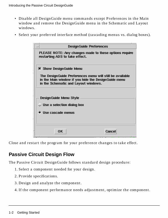
DesignGuides can be accessed in the Schematic window through either cascadingmenus or dialog boxes. You can configure your preferred method in the Main,Schematic, or Layout window. Choosing Preferences brings up a dialog box thatenables you to:
Note Use the dialog box menu style on Windows systems because resource issuestypically make the operating system unstable.
Getting Started 1-1
Introducing the Passive Circuit DesignGuide
• Disable all DesignGuide menu commands except Preferences in the Mainwindow and remove the DesignGuide menu in the Schematic and Layoutwindows.
• Select your preferred interface method (cascading menus vs. dialog boxes).
Close and restart the program for your preference changes to take effect.
Passive Circuit Design Flow
The Passive Circuit DesignGuide follows standard design procedure:
1. Select a component needed for your design.
2. Provide specifications.
3. Design and analyze the component.
4. If the component performance needs adjustment, optimize the component.
1-2 Getting Started
There are two important general concepts: SmartComponents and AutomatedAssistants.
SmartComponents
The DesignGuide provides a large number of passive SmartComponents such ascouplers, filters, and matching networks. SmartComponents contain specificationparameters and a schematic representation of the design.
SmartComponents are manipulated using several Automated Assistants. Theseassistants enable you to easily design, simulate, and optimize the SmartComponents.
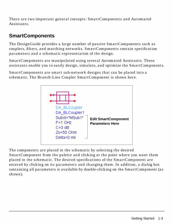
SmartComponents are smart sub-network designs that can be placed into aschematic. The Branch-Line Coupler SmartComponent is shown here.
The components are placed in the schematic by selecting the desiredSmartComponent from the palette and clicking at the point where you want themplaced in the schematic. The desired specifications of the SmartComponent areentered by clicking on its parameters and changing them. In addition, a dialog boxcontaining all parameters is available by double-clicking on the SmartComponent (asshown).
Edit SmartComponentParameters Here
Getting Started 1-3
Introducing the Passive Circuit DesignGuide
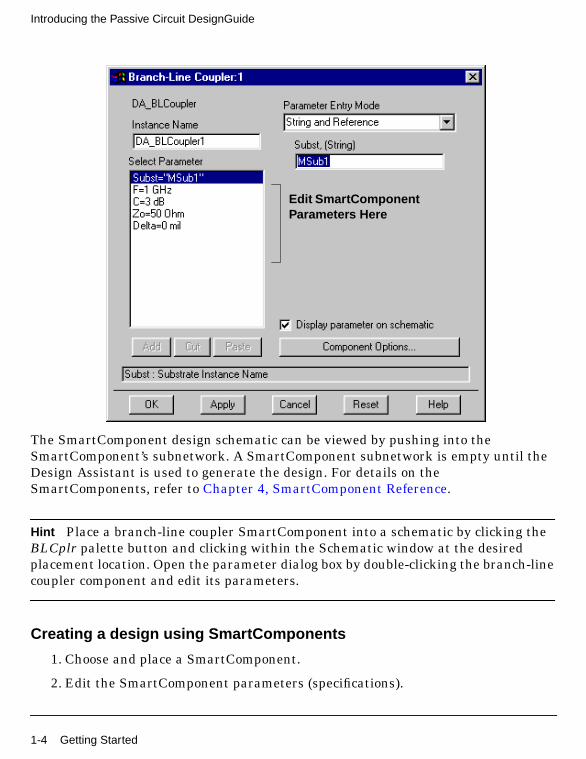
The SmartComponent design schematic can be viewed by pushing into theSmartComponent’s subnetwork. A SmartComponent subnetwork is empty until theDesign Assistant is used to generate the design. For details on theSmartComponents, refer to Chapter 4, SmartComponent Reference.
Hint Place a branch-line coupler SmartComponent into a schematic by clicking theBLCplr palette button and clicking within the Schematic window at the desiredplacement location. Open the parameter dialog box by double-clicking the branch-linecoupler component and edit its parameters.
Creating a design using SmartComponents
1. Choose and place a SmartComponent.
2. Edit the SmartComponent parameters (specifications).
Edit SmartComponentParameters Here
1-4 Getting Started
3. Design the SmartComponent using the Design Assistant.
4. Analyze the SmartComponent’s performance using the Simulation Assistant.
5. Display the performance of the SmartComponent using the Display Assistant.
6. If necessary, optimize the SmartComponent’s performance using theOptimization Assistant.
7. Re-analyze the SmartComponent’s performance using the SimulationAssistant.
Automated Assistants
The Passive Circuit DesignGuide provides four Automated Assistants for thesimplified design, simulation, optimization, and analysis of SmartComponents. EachAutomated Assistant has a tab that is accessed from DesignGuide Control Window.
Design Assistant is used to generate/update a SmartComponent’sschematic design. After a SmartComponent is placed and the parametersare specified, you start the Design Assistant to design the component.Subsequently, if the parameters of the SmartComponent are modified, youstart the Design Assistant again to update the design. For moreinformation, refer to “Design Assistant” on page 3-1.
Simulation Assistant is used to automatically perform a simulation of aSmartComponent. After a SmartComponent has been designed using theDesign Assistant, you start the Simulation Assistant to automaticallyanalyze the component. You can easily examine the simulation resultsusing the Display Assistant. For more information, refer to “SimulationAssistant” on page 3-2.
Getting Started 1-5
Introducing the Passive Circuit DesignGuide
Accessing the DesignGuide
The Passive Circuit DesignGuide is accessed from a Schematic window within ADS.
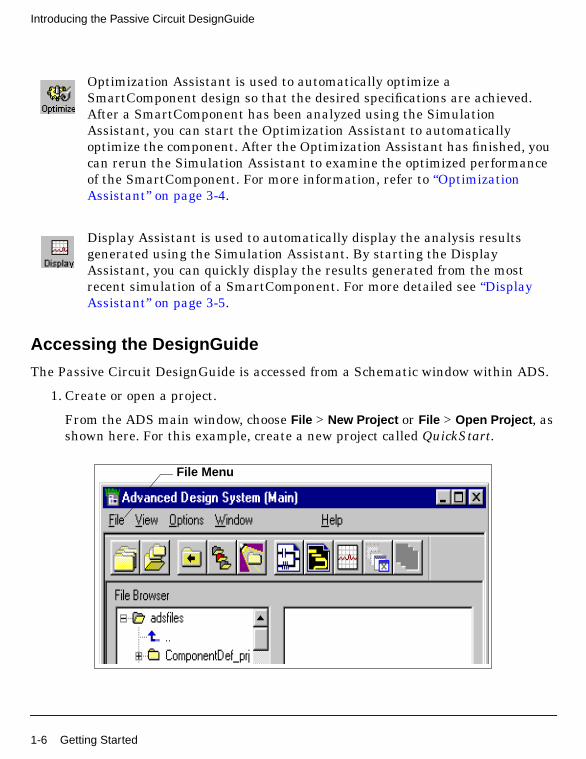
1. Create or open a project.
From the ADS main window, choose File > New Project or File > Open Project , asshown here. For this example, create a new project called QuickStart.
Optimization Assistant is used to automatically optimize aSmartComponent design so that the desired specifications are achieved.After a SmartComponent has been analyzed using the SimulationAssistant, you can start the Optimization Assistant to automaticallyoptimize the component. After the Optimization Assistant has finished, youcan rerun the Simulation Assistant to examine the optimized performanceof the SmartComponent. For more information, refer to “OptimizationAssistant” on page 3-4.
Display Assistant is used to automatically display the analysis resultsgenerated using the Simulation Assistant. By starting the DisplayAssistant, you can quickly display the results generated from the mostrecent simulation of a SmartComponent. For more detailed see “DisplayAssistant” on page 3-5.
File Menu
1-6 Getting Started

2. To open a Schematic window, choose Window > New Schematic or click the NewSchematic Window toolbar button.
A new Schematic window appears, as shown here. The DesignGuide featuresare accessed using the menu, Control Window, and SmartComponent palettes.
To access the Passive Circuit DesignGuide features:
1. From the Schematic window, DesignGuide > Passive Circuit .
2. To access the Control Window, choose Passive Circuit Control Window from thePassive Circuit menu.
3. To access the documentation for the DesignGuide, choose either of thefollowing:
• DesignGuide > Passive Circuit > Passive Circuit DesignGuide Documentation(from ADS Schematic window)
• Help > Topics and Index > DesignGuides > Passive Circuit (from any ADSprogram window)
New Schematic Window
Getting Started 1-7

Introducing the Passive Circuit DesignGuide
Note Depending on how your ADS preferences are set, a Schematic window mayautomatically appear when you create or open a project.
MenuSmartComponent Palette
1-8 Getting Started
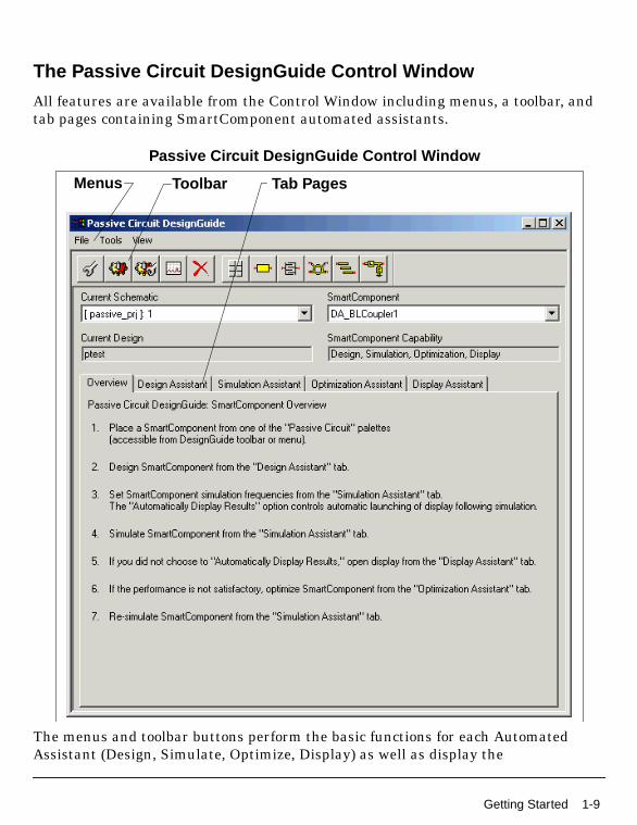
The Passive Circuit DesignGuide Control Window
All features are available from the Control Window including menus, a toolbar, andtab pages containing SmartComponent automated assistants.
The menus and toolbar buttons perform the basic functions for each AutomatedAssistant (Design, Simulate, Optimize, Display) as well as display the
ToolbarMenus
Passive Circuit DesignGuide Control Window
Tab Pages
Getting Started 1-9
Introducing the Passive Circuit DesignGuide
SmartComponent palettes. Full features are available from each of the tab pages onthe window. Explore each Automated Assistant tab page by clicking on the tab at thetop of each page. Explore the window menus as well to familiarize yourself with thebasic DesignGuide capabilities.
The window includes the following features and functions:
• You can place the window anywhere on the screen.
• With the fields at the top of the Control Window, you can navigate multipleSchematic windows and SmartComponents.
• The Current Schematic drop-down list box enables you to select any of thecurrently opened Schematic windows. This field is also updated when PassiveCircuit Control Window is selected from the Passive Circuit menu.
• The current design name is also displayed below the Current Schematic. TheSmartComponent drop-down list box enables you to select any of theSmartComponents on the currently selected Schematic window.
• The SmartComponent Capability field informs you of what functions (design,simulate, optimize, and display) the DesignGuide can perform for thatparticular component.
• To close the Control Window, choose File > Exit DesignGuide from the ControlWindow menu bar. The window may also be closed using the window closefeature of the operating system (a button marked with an ‘x’ at the top of thewindow).
SmartComponent Palette Access
The SmartComponent palettes are displayed by using the Control Window menusand toolbar. (They can also be chosen from the palette list box in the Schematicwindow toolbar.) Six palettes are available for accessing the SmartComponents. ThePassive Circuit palette contains all of the passive SmartComponents. The other fivepalettes group the components by their functionality. A blue accent in the upper-leftcorner of a palette button indicates the component is a SmartComponent.
1-10 Getting Started
Using the Passive Circuit DesignGuideThis step-by-step example will take you through the design of a microstrip line, andthe design, analysis and optimization of a branch-line coupler. After completing theseexamples, you should have a basic understanding of the DesignGuide.
Create a New Design
A new schematic design is needed to contain the microstrip line and branch-linecoupler for the following exercises. Follow these simple steps to create a new designnamed Example.
1. Open a new Schematic window.
2. Choose File > New Design from the Schematic window to create a Analog/RFNetwork design named Example.
Open the DesignGuide Control Window
1. From the DesignGuide menu on the ADS Schematic window, choose PassiveCircuit .
2. From the Passive Circuit window, choose Microstrip Control Window and clickOK.
Using the Passive Circuit DesignGuide 1-11
Introducing the Passive Circuit DesignGuide
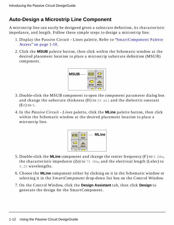
Auto-Design a Microstrip Line Component
A microstrip line can easily be designed given a substrate definition, its characteristicimpedance, and length. Follow these simple steps to design a microstrip line.
1. Display the Passive Circuit - Lines palette. Refer to “SmartComponent PaletteAccess” on page 1-10.
2. Click the MSUB palette button, then click within the Schematic window at thedesired placement location to place a microstrip substrate definition (MSUB)component.
3. Double-click the MSUB component to open the component parameter dialog boxand change the substrate thickness (H) to 20 mil and the dielectric constant(Er) to 5.
4. In the Passive Circuit - Lines palette, click the MLine palette button, then clickwithin the Schematic window at the desired placement location to place amicrostrip line.
5. Double-click the MLine component and change the center frequency (F) to 5 GHz,the characteristic impedance (Zo) to 75 Ohm, and the electrical length (Lelec) to0.25 wavelengths.
6. Choose the MLine component either by clicking on it in the Schematic window orselecting it in the SmartComponent drop-down list box on the Control Window.
7. On the Control Window, click the Design Assistant tab, then click Design togenerate the design for the SmartComponent.
MSUB
MLine
1-12 Using the Passive Circuit DesignGuide
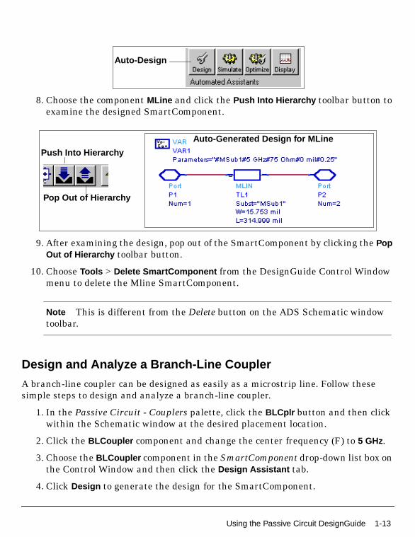
8. Choose the component MLine and click the Push Into Hierarchy toolbar button toexamine the designed SmartComponent.
9. After examining the design, pop out of the SmartComponent by clicking the PopOut of Hierarchy toolbar button.
10. Choose Tools > Delete SmartComponent from the DesignGuide Control Windowmenu to delete the Mline SmartComponent.
Note This is different from the Delete button on the ADS Schematic windowtoolbar.
Design and Analyze a Branch-Line Coupler
A branch-line coupler can be designed as easily as a microstrip line. Follow thesesimple steps to design and analyze a branch-line coupler.
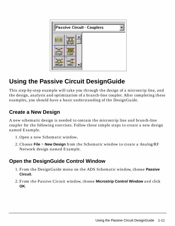
1. In the Passive Circuit - Couplers palette, click the BLCplr button and then clickwithin the Schematic window at the desired placement location.
2. Click the BLCoupler component and change the center frequency (F) to 5 GHz.
3. Choose the BLCoupler component in the SmartComponent drop-down list box onthe Control Window and then click the Design Assistant tab.
4. Click Design to generate the design for the SmartComponent.
Auto-Design
Push Into Hierarchy
Auto-Generated Design for MLine
Pop Out of Hierarchy
Using the Passive Circuit DesignGuide 1-13

Introducing the Passive Circuit DesignGuide
5. Click the Simulation Assistant tab on the Control Window and enter1 GHz start frequency, 10 GHz stop, 20 MHz step (accept default displayspecifications).
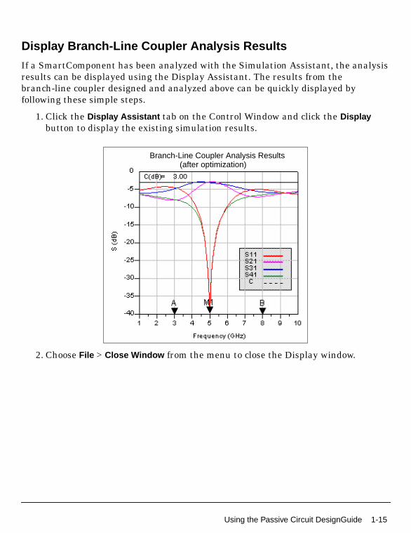
6. Click Simulate to analyze the SmartComponent. The analysis results are shownhere.
7. Close the Display window by choosing File > Close Window from the menu.
Optimize the Branch-Line Coupler
The branch-line coupler as designed in the preceding section has a center frequencyof 5.5 GHz, which is different from the desired 5 GHz. The difference is due tolimitations of the synthesis method used to generate the design. However, theOptimization Assistant can be used to easily optimize the design so that the centerfrequency is as specified.
1. Click the Optimization Assistant tab on the Control Window and click Optimize tooptimize the SmartComponent.
2. Click the Simulation Assistant tab on the Control Window
3. Deselect the Automatically display results check box.
4. Click Simulate to re-analyze the branch-line coupler.
Branch-Line Coupler Analysis Results
1-14 Using the Passive Circuit DesignGuide
Display Branch-Line Coupler Analysis Results
If a SmartComponent has been analyzed with the Simulation Assistant, the analysisresults can be displayed using the Display Assistant. The results from thebranch-line coupler designed and analyzed above can be quickly displayed byfollowing these simple steps.
1. Click the Display Assistant tab on the Control Window and click the Displaybutton to display the existing simulation results.
2. Choose File > Close Window from the menu to close the Display window.
Branch-Line Coupler Analysis Results(after optimization)
Using the Passive Circuit DesignGuide 1-15

Introducing the Passive Circuit DesignGuide
1-16 Using the Passive Circuit DesignGuide

Chapter 2: Using SmartComponentsThis chapter describes how to use SmartComponents to design your passive circuit.
OverviewSmartComponents are smart sub-network designs that can be placed into aschematic and provide the container for specification parameters and a schematicrepresentation of the design.
This DesignGuide provides a large number of passive SmartComponents such ascouplers, filters, lines and matching networks. Several automated-assistants enableyou to easily design, simulate (analyze), and optimize the SmartComponents.
SmartComponents can be placed, copied, edited and deleted like other components inthe Advanced Design System. The basics of placement, copying, editing and deletingare described here.
The DesignGuide contains six SmartComponent palettes that provide quick and easyaccess to the SmartComponents. The six available component palettes are:
• All contains all of the SmartComponents.
• Lines contains the simple line element SmartComponents.
• RLC contains the distributed resistor, inductor, and capacitorSmartComponents.
• Couplers contains the coupler and power divider SmartComponents.
• Filters contains the distributed filter SmartComponents.
• Match contains the distributed and lumped matching SmartComponents.
There are two methods to display the desired SmartComponent palette:
Open the Passive Circuit DesignGuide Control Window by choosing DesignGuide >Passive Circuit DesignGuide > Passive DesignGuide Control Window . Display thedesired SmartComponent palette by clicking one of the Component Palette buttonsfrom the Control Window toolbar or by choosing View > Component Palette - <PaletteName> from the Control Window menu.
Choose the desired SmartComponent palette from the Component Palette drop-downlist box in the Schematic window toolbar (directly above the palette).
Overview 2-1
Using SmartComponents
Placing SmartComponentsTo place a SmartComponent:
1. Click on the desired component button in a SmartComponent palette.
2. Click within the Schematic window at the location you want theSmartComponent placed.
3. You may change the orientation of the SmartComponent before placement bychoosing from the Insert > Component > Component Orientation commands or byrepeatedly clicking Rotate by -90 from the schematic toolbar.
4. The place component mode will remain active until you choose End Commandfrom the Schematic toolbar.
Note When a SmartComponent is initially placed, a temporary component is used toinitially place and specify the parameters for the SmartComponent. This componentdoes not contain a subnetwork design. After the Design Assistant has been used todesign the SmartComponent, the temporary component is replaced with a permanentcomponent. The SmartComponent is renamed to DA_ComponentName_DesignNameand an autogenerated design is placed inside the SmartComponent’s subnetworkdesign file. Subsequently, if the SmartComponent parameters are edited, the DesignAssistant will need to be used again to update the subnetwork design file.
Copying SmartComponentsSmartComponents can be copied within a design, to another design, or to anotherSchematic window.
Copying Within A Design
1. Click the SmartComponent to be copied.
2. Choose Edit > Copy, then Edit > Paste from the schematic window.
3. Click the spot where you want the copy placed.
2-2 Placing SmartComponents

Copying Between Designs or Schematic Windows
1. Click the SmartComponent to be copied.
2. Choose Edit > Copy from the Schematic window.
3. Display the design or Schematic window you want to copy the SmartComponentto.
4. Choose Edit > Paste to copy the SmartComponent to the design.
5. Click where you want the component placed.
Note All copied SmartComponents will initially refer to the same SmartComponentdesign. When the Design Assistant is used to perform a design operation, it willtransform each copied SmartComponent into a unique SmartComponent design. Adesign operation is accomplished by launching the Design Assistant from theDesignGuide Control Window.
Editing SmartComponentsA SmartComponent’s position, orientation, and parameters can be edited like anyother component in ADS.
Position and Orientation
A SmartComponent is moved by dragging it to any location in the Schematic window.It’s orientation is changed by following these steps.
1. Choose Edit > Advanced Rotate/Mirror > Rotate from the Schematic window orclick Rotate Items from the toolbar.
2. Click on the desired SmartComponent.
3. Rotate the component.
4. The rotate mode will remain active until you select the End Command from thetoolbar.
Editing SmartComponents 2-3
Using SmartComponents
Parameters
Parameters are changed by clicking on a SmartComponent parameter in theSchematic window and editing it or by double-clicking a component and editing theparameters in the component dialog box.
Deleting SmartComponentsSmartComponents can be deleted from a design like other components, butcompletely removing a SmartComponent’s files requires the actions described here.
Delete From Current Design
A SmartComponent can be deleted from a design by choosing the component andpressing the Delete key, clicking the Delete button on the toolbar, or by choosing Edit >Delete from the Schematic window. However, this does not remove theSmartComponent files from the project directory.
Delete From Current Project
To delete a SmartComponent and all associated files from your project, follow thesesteps.
1. From the DesignGuide Control Window, click the Delete SmartComponentbutton.
2. Click on the SmartComponent you want deleted. This will delete theSmartComponent from the current design and remove all of its files from yourproject.
3. The SmartComponent delete mode will remain active until you choose the EndCommand from the Schematic toolbar.
Delete Manually Using File System
You may use your computer’s file system to delete a SmartComponent by deleting theappropriate files in the network subdirectory of a project. Delete files that start withDA_, SA_’ and OA_, contain the SmartComponent title, and end with .ael or .dsn.
2-4 Deleting SmartComponents
Design, Analysis, Optimization and LayoutThe DesignGuide contains several automated assistants that provide automaticdesign, analysis, and optimization for the SmartComponents. The followingassistants are available.
• Design Assistant. The Design Assistant is used to generate and update thedesign contained within a SmartComponent. It invokes a synthesis engine thatgenerates a design from the given specification. It will design and update asingle SmartComponent or all SmartComponents in a design. Refer to “DesignAssistant” on page 3-1 for more information.
• Simulation (Analysis) Assistant. The Simulation Assistant is used to analyze thedesign contained within a SmartComponent. It creates a simulation circuitcontaining the SmartComponent, then performs a simulation. It can alsoautomatically display the results of the simulation. Refer to “SimulationAssistant” on page 3-2 for more information.
• Optimization Assistant. The Optimization Assistant is used to optimize thedesign contained within a SmartComponent. It creates an optimization circuitcontaining the SmartComponent, performs an optimization, and updates theSmartComponent. Refer to “Optimization Assistant” on page 3-4 for moreinformation.
• Display Assistant . The Display Assistant is used to quickly display theperformance of a SmartComponent. Display templates have been created formost of the SmartComponents. The display templates are preconfiguredtemplates which provide a comprehensive look at the component’s performance.Refer to “Display Assistant” on page 3-5 for more information.
• Automatic Layout Generation . Artwork for all of the passive circuitSmartComponents in this DesignGuide can be automatically generated. Thesynthesis engine used by the Design Assistant creates a schematic for theSmartComponents that is auto-layout-generation ready. The Generate Layoutcapability of ADS is used to generate the artwork for the SmartComponents.Refer to “Layout Generation” on page 3-9 for more information.
Stand-Alone SmartComponent UsageOnce SmartComponents are designed and tested, they can be used as stand-alonecomponents. The Passive Circuit DesignGuide is not needed to use them in newdesigns unless you wish to modify or analyze them.
Design, Analysis, Optimization and Layout 2-5
Using SmartComponents
Using an Existing SmartComponent Within the Same Project
1. Open the Component Library window by choosinging Insert > Component >Component Library from the Schematic window or Display Component LibraryList from the toolbar.
2. Choose the project name under All > Sub-networks in the Libraries list at theleft of the Component Library window. Available components will be listed inthe Components list at the right of the Component Library window.
3. Choose the desired SmartComponent in the Components list.
4. Place the desired SmartComponent into your design by clicking in theSchematic window at the location you wish it placed. The insert mode willremain active until you click End Command on the toolbar.
Using an Existing SmartComponent in Any Project
A library of predesigned reusable SmartComponents can be easily created. This isdone by placing the reusable SmartComponents in a project. This project can beincluded in any project and its SmartComponents will be accessed using theComponent Library. Follow these steps.
1. Choose File > Include/Remove Projects from the main ADS window.
2. Choose the project that contains the desired SmartComponent from the FileBrowser at the left of the Include & Remove window.
3. Click the Include button to include the project in the hierarchy.
4. Click OK.
5. Open the Component Library window by choosing Insert > Component >Component Library from the Schematic window or Display Component LibraryList from the toolbar.
6. Choose the included project name under All > Sub-networks in the Libraries listat the left of the Component Library window. Available components will belisted in the Components list at the right of the Component Library window.
7. Choose the desired SmartComponent in the Components list.
8. Place the desired SmartComponent into your design by clicking in theSchematic window at the location you wish it placed. The insert mode willremain active until you select End Command from the toolbar.
2-6 Stand-Alone SmartComponent Usage
Chapter 3: Using Automated AssistantsThis chapter describes the four Automated Assistants used to design, simulate,optimize, and analyze SmartComponents, followed by instructions for creating layoutartwork from the DesignGuide.
Design AssistantThe Design Assistant is used to generate and update the design contained within aSmartComponent from the given specifications. It will design and update a singleSmartComponent or all SmartComponents in a design.
The Design Assistant is accessed using the Passive Circuit DesignGuide ControlWindow. From the Control Window, full design control is enabled from the DesignAssistant tab. Single component design operations can also be accomplished usingthe Control Window menu and toolbar.
Single Component Design
To design a single SmartComponent using the Control Window, select the desiredSmartComponent either from the SmartComponent drop-down list box in the upperright corner of the Control Window or by clicking on the component in the Schematicwindow. The design is accomplished using one of the following methods.
• Click the Design button on the Design Assistant tab. The design progress isindicated on the tab page.
• Click the Design button on the Control Window toolbar.
• Choose Tools > Auto-Design from the Control Window menu.
Multiple Component Design
Clicking the Design All button on the Design Assistant tab designs allSmartComponents on the current Schematic.
Note To avoid screen flicker associated with the design, the Schematic window willdisappear during the process.
Design Assistant 3-1
Using Automated Assistants
Design progress is indicated on the tab page.
Simulation AssistantThe Simulation Assistant is used to analyze the design contained within aSmartComponent. It creates a simulation circuit around the SmartComponent, thenperforms a simulation. If desired it will automatically display the simulation results.
The Simulation Assistant is accessed using the Passive Circuit DesignGuide ControlWindow. From the Control Window, full simulation control is enabled from theSimulation Assistant tab. Basic simulation can also be accomplished using theControl Window menu and toolbar.
For all simulation operations, the selected SmartComponent is designed if necessary,a simulation schematic is created, the simulation is performed, and the results aredisplayed. The simulation frequency sweep must be specified on the SimulationAssistant tab in the Control window.
Note When the Simulation Assistant is used, the simulation schematic is deletedautomatically. To retain the schematic that is created, instead of the SimulationAssistant, use the Create Template option described in “Using SimulationTemplates” on page 3-3.
Simulation Frequency Sweep
The simulation frequency sweep is specified on the Passive Circuit DesignGuideControl Window. If you are performing the simulation from the Control Window, clickthe Simulation Assistant tab and specify the sweep by entering the start frequency,stop frequency, and either frequency step size or number of points. The valuesentered are stored in the selected SmartComponent (as displayed in theSmartComponent drop-down list box) and will be recalled each time thisSmartComponent is selected.
Note If a SmartComponent has been selected from the SmartComponent drop-downlist box on the Control Window, default frequencies will be set for the component.
3-2 Simulation Assistant
Automatically Display Results
If the Automatically Display Results box on the Control Window’s SimulationAssistant tab is selected, the simulation results will be automatically displayed uponcompletion of the analysis.
To Simulate a SmartComponent
To simulate a SmartComponent using the Control Window, select the desiredSmartComponent either from the SmartComponent drop-down list box in the upperright corner of the Control Window or by clicking on the component on the schematicwindow.
The simulation frequency sweep display option must be specified on the SimulationAssistant tab as previously described.
The simulation is then accomplished using one of the following methods:
• Click Simulate on the Simulation Assistant tab.
• Click Simulate on the Control Window toolbar.
• Choose Tools > Auto-Simulate from the Control Window menu.
Using Simulation Templates
In some cases, such as when you would like to retain the schematic that is created, itis useful to simulate the SmartComponent manually.
To generate a simulation schematic around the selected SmartComponent, click theCreate Template button on the Control Window Simulation Assistant tab.
You can examine or modify the simulation schematic, then manually start thesimulation by choosing Simulate > Simulate from the Schematic window.
When you are finished, clicking the Update from Template button on the SimulationAssistant tab will transfer any changes you have made to the SmartComponent onthe Simulation schematic to the original SmartComponent and redesign if necessary.
You can also manually close the simulation schematic by choosing File > Close Designfrom the Schematic window menu, although this will result is loss of any changes youhave made to the SmartComponent.
Simulation Assistant 3-3
Using Automated Assistants
Optimization AssistantThe Optimization Assistant is used to optimize the design contained within aSmartComponent. It creates a optimization circuit containing the SmartComponent,then performs an optimization.
The assistant is accessed using the Passive Circuit DesignGuide Control Window.From the Control Window, full optimization control is enabled from the OptimizationAssistant tab. Basic optimization can also be accomplished using the Control Windowmenu and toolbar.
The Optimization Assistant contains fields that indicate the objective of theoptimization operation as well as the physical parameters to be altered during theprocess.
For all optimization operations, the selected SmartComponent is designed (ifnecessary), an optimization schematic is created, and the optimization is performed.The optimization results are transferred to the original SmartComponent, and thisaltered component is redesigned.
For each component, the optimization alters one or more of the physical designdimensions in order to make the component response more closely meet the specifiedperformance.
To Optimize a SmartComponent
To optimize a SmartComponent using the Control Window, follow these steps.
1. Select the desired SmartComponent either from the SmartComponentdrop-down list box in the upper right corner of the Control Window or byclicking on the component on the schematic window.
2. Optimize the component by either:
• Pushing the Optimize button on the Optimization Assistant tab
• Pushing the Optimize button on the Control Window toolbar
• Selecting Tools > Auto-Optimize from the Control Window menu
Optimization Templates
In some cases it may be useful to manually optimize the SmartComponent.
3-4 Optimization Assistant
To generate an optimization schematic around the selected SmartComponent, pressthe Create Template button on the Control Window Optimization Assistant tab.
You can examine or modify the optimization schematic, then manually start theoptimization by selecting Simulate > Simulate from the Schematic window.
When you are finished, selecting Simulate > Update Optimization Values will cause theoptimized values to appear in the VAR element in the schematic lower left corner foryour inspection.
Pressing the Update from Template button on the Optimization Assistant tab willtransfer the optimization results to the original SmartComponent and redesign.
You may also manually close the optimization schematic using File > Close Designfrom the Schematic window menu, although this will cause optimization results to belost.
Display AssistantThe Display Assistant is used to easily and quickly display the performance of aSmartComponent.
The Display Assistant is accessed using either the Passive Circuit DesignGuideControl Window. From the Control Window, full display control is enabled from theDisplay Assistant tab. Basic display selection can also be accomplished using theControl Window menu and toolbar.
Display Templates
The display templates are preconfigured templates that provide a comprehensivelook at the performance of the component. Display templates have been created formost of the SmartComponents. This includes all of the RLC, coupler, filter andmatching components. The line components do not have auto-simulation,auto-optimization or auto-display capability because of their simplicity.
You can create your own displays or modify the included display templates using thebuilt in features of Advanced Design System, but in most situations, the includeddisplay templates will provide all the information you need.
The display templates opened by the Display Assistant have common features thatare discussed here. For features unique to the display templates of someSmartComponents, refer to Chapter 4, SmartComponent Reference.
Display Assistant 3-5
Using Automated Assistants
In some cases it may be useful to use one of the display templates provided with theDesignGuide for other applications.
To gain access to one of these templates, select the desired template from theAvailable Templates field and press the Open Display Template button on the ControlWindow Display Assistant tab.
You can then insert a dataset of your choice using the dataset pull-down list box inthe upper left corner of the display. You may find that some parameters in the displaytemplate are not defined in the selected dataset and may want to make appropriatemodifications to the display. These changes can be saved using the commands in thedisplay File menu.
Basic Layout
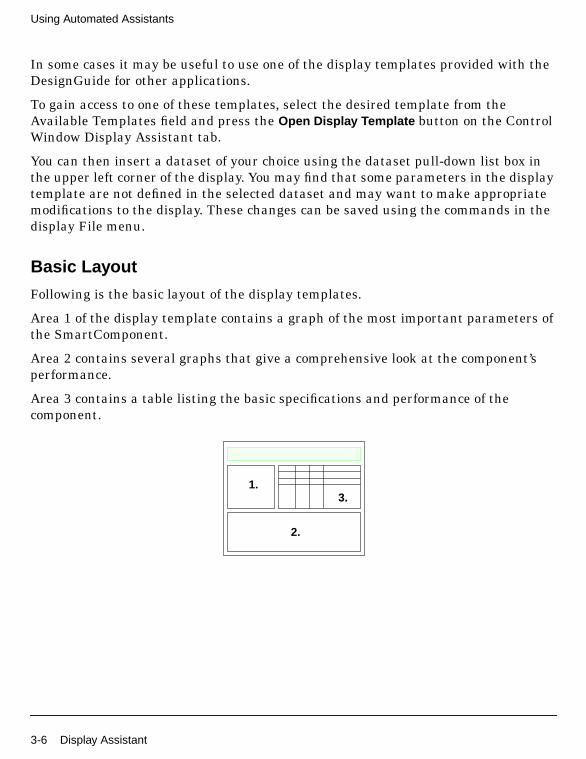
Following is the basic layout of the display templates.
Area 1 of the display template contains a graph of the most important parameters ofthe SmartComponent.
Area 2 contains several graphs that give a comprehensive look at the component’sperformance.
Area 3 contains a table listing the basic specifications and performance of thecomponent.
1.
2.
3.
3-6 Display Assistant
Typical Area 1 Content
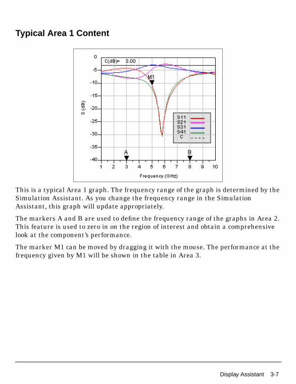
This is a typical Area 1 graph. The frequency range of the graph is determined by theSimulation Assistant. As you change the frequency range in the SimulationAssistant, this graph will update appropriately.
The markers A and B are used to define the frequency range of the graphs in Area 2.This feature is used to zero in on the region of interest and obtain a comprehensivelook at the component’s performance.
The marker M1 can be moved by dragging it with the mouse. The performance at thefrequency given by M1 will be shown in the table in Area 3.
Display Assistant 3-7
Using Automated Assistants
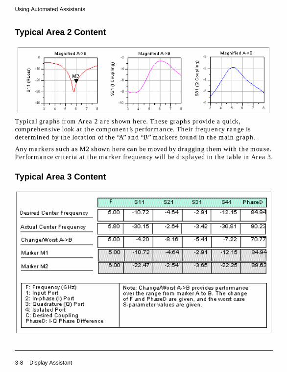
Typical Area 2 Content
Typical graphs from Area 2 are shown here. These graphs provide a quick,comprehensive look at the component’s performance. Their frequency range isdetermined by the location of the “A” and “B” markers found in the main graph.
Any markers such as M2 shown here can be moved by dragging them with the mouse.Performance criteria at the marker frequency will be displayed in the table in Area 3.
Typical Area 3 Content
3-8 Display Assistant
A typical table from Area 3 is shown here. The white rows show the desiredspecifications and important performance criteria for the component. The gray rowsgive the performance criteria at the user defined marker frequencies. The box belowthe table provides explanatory information for the table.
To Display SmartComponent Performance Results
Before using the Display Assistant, a valid dataset from a simulation of the selectedSmartComponent must exist in the current project data directory. This simulationcan be conveniently accomplished using the Simulation Assistant. Refer to“Simulation Assistant” on page 3-2 for details on this step.
To display results from a SmartComponent simulation using the Control Window,select the desired SmartComponent either from the SmartComponent drop-down listbox in the upper right corner of the Control Window or by clicking on the componenton the schematic window. The display is then launched using one of the followingmethods.
• Push the Display button on the Display Assistant tab.
• Push the Display button on the Control Window toolbar.
• Select Tools > Auto-Display from the Control Window menu.
If no valid dataset exists for the selected SmartComponent, the Display button on theDisplay Assistant tab will be insensitive. If the toolbar or menu are used to try todisplay the results, a message will appear indicating that no dataset exists.
Layout GenerationThe Design Assistant creates a schematic for the SmartComponents that is ready forauto-layout generation. Artwork for all of the Passive Circuit DesignGuideSmartComponents can be automatically generated. The ADS Generate Layoutcapability is used to generate the artwork for the SmartComponents.
Note You need an Advanced Design System Layout license to use this feature.
Layout Generation 3-9
Using Automated Assistants
Creating Layout Artwork
To create artwork for SmartComponents, follow these steps:
1. Choose and place the desired SmartComponents in the schematic window.
2. Specify the desired parameters for each SmartComponent.
3. Design the SmartComponents using the Design Assistant.
4. Select Layout > Generate/Update Layout from the Schematic window.
5. Choose OK in the Generate/Update Layout box.
The artwork for each SmartComponent and any other components that haveassociated artwork will be displayed in the Layout window. If the status reportcheckbox is selected in the Generate/Update Layout box, a layout generation statusreport will also be opened.
Updating Layout Artwork
To edit the properties of a SmartComponent and update the associated artwork,follow these steps:
1. Choose the desired SmartComponent in the schematic window.
2. Edit the desired parameters of the SmartComponent.
3. Design the SmartComponent using the Design Assistant.
4. Select Layout > Generate/Update Layout from the Schematic window.
5. Select OK in the Generate/Update Layout box.
The artwork for the SmartComponent will be updated and displayed in the layoutwindow.
3-10 Layout Generation
te the
Chapter 4: SmartComponent ReferenceThis chapter provides detailed information for all passive circuit SmartComponents.
SmartComponent List
Note A SmartComponent subnetwork is empty until the Design Assistant is used to generadesign. Refer to“Design Assistant” on page 3-1.
Passive Circuit DG - Lines
MBend (Microstrip Bend Component)
MBStub (Microstrip Butterfly Radial Stub)
MCFil (Microstrip Coupled-Line Filter Element)
MCLine (Microstrip Coupled Line Component)
MCorn (Microstrip Corner Component)
MCross (Microstrip Cross Component)
MCurve (Microstrip Curve Component)
MGap (Microstrip Gap Component)
MLine (Microstrip Line)
MMndr (Microstrip Meander Line)
MRStub (Microstrip Radial Stub)
MStep (Microstrip Step Component)
MStub (Microstrip Stub)
MTaper (Microstrip Taper Component)
MTee (Microstrip Tee Component)
SmartComponent List 4-1
SmartComponent Reference
Passive Circuit DG - RLC
MICapP (Microstrip 4-port Interdigital Capacitor)
MICapPG (Microstrip Grounded 2-port Interdigital Capacitor)
MICapS (Microstrip 2-port Interdigital Capacitor)
MICapSG (Microstrip 1-port Interdigital Capacitor)
MREInd (Microstrip Elevated Rectangular Inductor)
MRInd (Microstrip Rectangular Inductor)
MSInd (Microstrip Spiral Inductor)
MTFC (Microstrip Thin Film Capacitor)
TFC (Thin Film Capacitor)
TFR (Thin Film Resistor)
Passive Circuit DG - Couplers
BLCoupler (Branch-Line Coupler)
CLCoupler (Coupled-Line Coupler)
LCoupler (Lange Coupler)
RRCoupler (Rat-Race Coupler)
TCoupler (Tee Power Divider)
WDCoupler (Wilkinson Divider)
Passive Circuit DG - Filters
CLFilter (Coupled-Line Filter)
CMFilter (Comb-Line Filter)
HPFilter (Hairpin Filter)
IDFilter (Interdigital Filter)
SBFilter (Stub Bandpass Filter)
SIFilter (Stepped Impedance Lowpass Filter)
SLFilter (Stub Lowpass Filter)
4-2
SRFilter (Stepped Impedance Resonator Filter)
ZZFilter (Zig-Zag Coupled-Line Filter)
Passive Circuit DG - Matching
DSMatch (Double-Stub Match)
LEMatch (Lumped Component Match)
QWMatch (Quarter-Wave Match)
RAtten (Resistive Attenuator)
SSMatch (Single-Stub Match)
TLMatch (Tapered-Line Match)
SmartComponent List 4-3

SmartComponent Reference
e, and
nont.
ND
te the
Passive Circuit DG - Lines
MBend (Microstrip Bend Component)
Symbol
Parameters
Subst = microstrip substrate name
F = design frequency, in hertz
Zo = desired characteristic impedance, in ohms
BendType = type of bend
Angle = angle of bend (for arbitrary angle/miter bend)
M = miter fraction (for arbitrary angle/miter bend)
Notes
1. MBend designs a microstrip bend given the substrate, desired characteristic impedancbend properties. The design will realize the native MBEND, MBEND2, or MBEND3components.
2. Since the design uses the models inherent to ADS to compute the line width, there isneed for a dedicated Simulation Assistant, Optimization Assistant, or Display Assista
3. BendType can be Arbitrary Angle/Miter (MBEND), 90 Degree/Miter (MBEND2), or 90Degree/Optimal Miter (MBEND3). The parameters Angle and M are only used for MBErealizations. Refer to the discussion of these components in the ADS MicrostripComponents documentation for a more detailed description.
4. A SmartComponent subnetwork is empty until the Design Assistant is used to generadesign. Refer to“Design Assistant” on page 3-1.
4-4 MBend (Microstrip Bend Component)

stub
ce.
te the
MBStub (Microstrip Butterfly Radial Stub)
Symbol
Parameters
Subst = microstrip substrate name
F = design frequency, in hertz
Xin = desired input reactance, in ohms (only one of Xin, Cin, and Lin can be non-zero)
Cin = desired input capacitance, in farads (only one of Xin, Cin, and Lin can be non-zero)
Lin = desired input inductance, in henries (only one of Xin, Cin, and Lin can be non-zero)
W = width of feed line (set to zero if Z specified)
Z = characteristic impedance of feed line (set to zero if W specified)
Angle = subtended angle of circular sector
d = insertion depth of circular sector in feed line
Delta = length added to stub for tuning performance
Notes
1. MBStub designs a microstrip butterfly radial stub given the substrate, desired inputreactance, and stub dimensions.
2. The stub is designed by dividing the radial lines into several short segments.
3. For proper operation, only one of Xin, Cin, and Lin can be non-zero. If all are zero, theis designed to provide an open circuit.
4. Refer to the discussion of the MBSTUB component in the Microstrip Componentsdocumentation for a more detailed description of the model used for this component.
5. The optimization changes the length of the stubs to achieve the desired input reactan
6. A SmartComponent subnetwork is empty until the Design Assistant is used to generadesign. Refer to“Design Assistant” on page 3-1.
MBStub (Microstrip Butterfly Radial Stub) 4-5
SmartComponent Reference
Hz.
Example
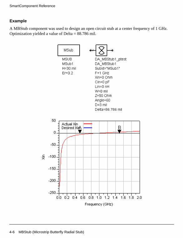
A MBStub component was used to design an open circuit stub at a center frequency of 1 GOptimization yielded a value of Delta = 88.786 mil.
4-6 MBStub (Microstrip Butterfly Radial Stub)
even-
nont.
vidednentodel
te the
MCFil (Microstrip Coupled-Line Filter Element)
Symbol
Parameters
Subst = microstrip substrate name
F = design frequency, in hertz
Zoe = desired even-mode characteristic impedance, in ohms
Zoo = desired odd-mode characteristic impedance, in ohms
Zo1 = characteristic impedance of input line at port 1, in ohms
Zo2 = characteristic impedance of input line at port 2, in ohms
Lphys = physical line length (set to zero if Lelec specified)
Lelec = line length in wavelengths (set to zero if Lphys specified)
Notes
1. MCFil designs a microstrip coupled-line filter component given the substrate, desiredand odd-mode characteristic impedances, and physical or electrical length.
2. Since the design uses the models inherent to ADS to compute the line width, there isneed for a dedicated Simulation Assistant, Optimization Assistant, or Display Assista
3. For proper operation, either Lphys or Lelec must be zero.
4. Zo1 and Zo2 specify the impedance of the lines attached to this component and are proto ensure proper pin location in the layout. Refer to the discussion of the MCFIL compoin the Microstrip Components documentation for a more detailed description of the mused for this component.
5. A SmartComponent subnetwork is empty until the Design Assistant is used to generadesign. Refer to“Design Assistant” on page 3-1.
MCFil (Microstrip Coupled-Line Filter Element) 4-7
SmartComponent Reference
n- and
nont.
areFIL
on of
te the
MCLine (Microstrip Coupled Line Component)
Symbol
Parameters
Subst = microstrip substrate name
F = design frequency, in hertz
Zoe = desired even-mode characteristic impedance, in ohms
Zoo = desired odd-mode characteristic impedance, in ohms
Zo1 = characteristic impedance of input line at port 1, in ohms
Zo2 = characteristic impedance of input line at port 2, in ohms
Zo3 = characteristic impedance of input line at port 3, in ohms
Zo4 = characteristic impedance of input line at port 4, in ohms
Lphys = physical line length (set to zero if Lelec specified)
Lelec = line length in wavelengths (set to zero if Lphys specified)
Notes
1. MCLine designs a microstrip coupled line component given the substrate, desired eveodd-mode characteristic impedances, and physical or electrical length.
2. Since the design uses the models inherent to ADS to compute the line width, there isneed for a dedicated Simulation Assistant, Optimization Assistant, or Display Assista
3. For proper operation, either Lphys or Lelec must be zero.
4. Zo1 through Zo4 specify the impedance of the lines attached to this component and provided to ensure proper pin location in the layout. Refer to the discussion of the MCcomponent in the Microstrip Components documentation for a more detailed descriptithe model used for this component.
5. A SmartComponent subnetwork is empty until the Design Assistant is used to generadesign. Refer to“Design Assistant” on page 3-1.
4-8 MCLine (Microstrip Coupled Line Component)

nont.
MCorn (Microstrip Corner Component)
Symbol
Parameters
Subst = microstrip substrate name
F = design frequency, in hertz
Zo = desired characteristic impedance, in ohms
Notes
1. MCorn designs a microstrip corner component given the substrate and characteristicimpedance of the input and output lines.
2. Note A SmartComponent subnetwork is empty until the Design Assistant is used togenerate the design. Refer to“Design Assistant” on page 3-1.
3. Since the design uses the models inherent to ADS to compute the line width, there isneed for a dedicated Simulation Assistant, Optimization Assistant, or Display Assista
4. Refer to the discussion of the MCORN component in the Microstrip Componentsdocumentation for a more detailed description of the model used for this component.
MCorn (Microstrip Corner Component) 4-9

SmartComponent Reference
nce onVE2
nont.
te the
MCross (Microstrip Cross Component)
Symbol
Parameters
Subst = microstrip substrate name
F = design frequency, in hertz
Z1 = characteristic impedance of port 1, in ohms
Z2 = characteristic impedance of port 2, in ohms
Z3 = characteristic impedance of port 3, in ohms
Z4 = characteristic impedance of port 4, in ohms
Notes
1. MCross designs a microstrip cross given the substrate, desired characteristic impedaeach port, and bend properties. The design will realize the native MCURVE and MCURcomponents.
2. Since the design uses the models inherent to ADS to compute the line width, there isneed for a dedicated Simulation Assistant, Optimization Assistant, or Display Assista
3. Refer to the discussion of the MCROSS component in the Microstrip Componentsdocumentation for a detailed description of this component.
4. A SmartComponent subnetwork is empty until the Design Assistant is used to generadesign. Refer to“Design Assistant” on page 3-1.
4-10 MCross (Microstrip Cross Component)

e, andents.
nont.
theore
te the
MCurve (Microstrip Curve Component)
Symbol
Parameters
Subst = microstrip substrate name
F = design frequency, in hertz
Zo = desired characteristic impedance, in ohms
Angle = angle of curve
Radius = radius of curvature (set to zero if Lelec specified)
Lelec = curve length in wavelengths (set to zero if Radius specified)
CurveType = type of curve
Nmode = number of modes (for Waveguide Model)
Notes
1. MBend designs a microstrip bend given the substrate, desired characteristic impedancbend properties. The design will realize the native MCURVE and MCURVE2 compon
2. Since the design uses the models inherent to ADS to compute the line width, there isneed for a dedicated Simulation Assistant, Optimization Assistant, or Display Assista
3. Either Lelec or Radius must be zero for proper operation.
4. BendType can be Transmission Line Model (MCURVE) or Magnetic Wall WaveguideModel (MCURVE2). The parameter Nmode is used only for MCURVE2. Refer to the todiscussion of these components in the Microstrip Components documentation for a mdetailed description.
5. A SmartComponent subnetwork is empty until the Design Assistant is used to generadesign. Refer to“Design Assistant” on page 3-1.
MCurve (Microstrip Curve Component) 4-11

SmartComponent Reference
, and
nont.
te the
MGap (Microstrip Gap Component)
Symbol
Parameters
Subst = microstrip substrate name
F = design frequency, in hertz
Zo = desired characteristic impedance, in ohms
S = length of gap (spacing)
Notes
1. MGap designs a microstrip gap given the substrate, desired characteristic impedancegap width.
2. Since the design uses the models inherent to ADS to compute the line width, there isneed for a dedicated Simulation Assistant, Optimization Assistant, or Display Assista
3. Refer to the discussion of the MGAP component in the Microstrip Componentsdocumentation for a detailed description of this component.
4. A SmartComponent subnetwork is empty until the Design Assistant is used to generadesign. Refer to“Design Assistant” on page 3-1.
4-12 MGap (Microstrip Gap Component)

, and
th,lay
te the
MLine (Microstrip Line)
Symbol
Parameters
Subst = microstrip substrate name
F = design frequency, in hertz
Zo = desired characteristic impedance, in ohms
Lphys = physical line length (set to zero if Lelec specified)
Lelec = line length in wavelengths (set to zero if Lphys specified)
Notes
1. MLine designs a microstrip line given the substrate, desired characteristic impedancephysical or electrical length.
2. Since the design uses the models inherent to ADS to compute the line width and lengthere is no need for a dedicated Simulation Assistant, Optimization Assistant, or DispAssistant.
3. For proper operation, either Lphys or Lelec must be zero.
4. Refer to the discussion of the MLIN component in the Microstrip Componentsdocumentation for a more detailed description of the model used for this component.
5. A SmartComponent subnetwork is empty until the Design Assistant is used to generadesign. Refer to“Design Assistant” on page 3-1.
MLine (Microstrip Line) 4-13

SmartComponent Reference
tic line.
rized
d thate thean
te the
MMndr (Microstrip Meander Line)
Symbol
Parameters
Subst = microstrip substrate name
F = design frequency, in hertz
Zo = desired characteristic impedance, in ohms
Lphys = physical line length (set to zero if Lelec specified)
Lelec = line length in wavelengths (set to zero if Lphys specified)
WR = bounding rectangle width, in meters
HR = bounding rectangle height, in meters
Delta = length added to vertical lines for tuning performance
Notes
1. MMndr designs a meandering microstrip line given the substrate, desired characterisimpedance, physical or electrical length, and maximum rectangular dimensions of the
2. The line input and output ports will be at the center of the rectangle on the side characteby HR.
3. The final width and height of the bounding box may be smaller than that specifieddepending on the desired length.
4. For proper operation, either Lphys or Lelec must be zero.
5. Refer to the discussion of the MLIN component in the Microstrip Componentsdocumentation for a more detailed description of the model used for this component.
6. The optimization minimizes the absolute difference between the transmission phase anresulting from the specified length. Only the vertical dimension is optimized, and sinccorners tend to add excess phase delay the resulting height will be slightly smaller thspecified.
7. A SmartComponent subnetwork is empty until the Design Assistant is used to generadesign. Refer to“Design Assistant” on page 3-1.
4-14 MMndr (Microstrip Meander Line)
a at a
Example
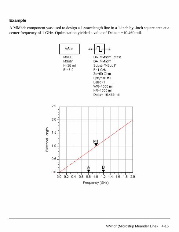
A MMndr component was used to design a 1-wavelength line in a 1-inch by -inch square arecenter frequency of 1 GHz. Optimization yielded a value of Delta =−10.469 mil.
MMndr (Microstrip Meander Line) 4-15

SmartComponent Reference
, and
stub
ce.
te the
MRStub (Microstrip Radial Stub)
Symbol
Parameters
Subst = microstrip substrate name
F = design frequency, in hertz
Xin = desired input reactance, in ohms (only one of Xin, Cin, and Lin can be non-zero)
Cin = desired input capacitance, in farads (only one of Xin, Cin, and Lin can be non-zero)
Lin = desired input inductance, in henries (only one of Xin, Cin, and Lin can be non-zero)
W = width of feed line (set to zero if Z specified)
Z = characteristic impedance of feed line (set to zero if W specified)
Angle = subtended angle of circular sector
Delta = length added to stub for tuning performance
Notes
1. MRStub designs a microstrip radial stub given the substrate, desired input reactancestub dimensions.
2. The stub is designed by dividing the radial line into several short segments.
3. For proper operation, only one of Xin, Cin, and Lin can be non-zero. If all are zero, theis designed to provide an open circuit.
4. Refer to the discussion of the MRSTUB component in the Microstrip Componentsdocumentation for a more detailed description of the model used for this component.
5. The optimization changes the length of the stubs to achieve the desired input reactan
6. A SmartComponent subnetwork is empty until the Design Assistant is used to generadesign. Refer to“Design Assistant” on page 3-1.
4-16 MRStub (Microstrip Radial Stub)
Hz.
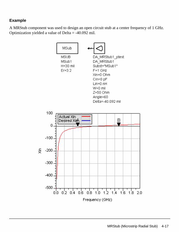
Example
A MRStub component was used to design an open circuit stub at a center frequency of 1 GOptimization yielded a value of Delta = -40.092 mil.
MRStub (Microstrip Radial Stub) 4-17

SmartComponent Reference
ances.
nont.
te the
MStep (Microstrip Step Component)
Symbol
Parameters
Subst = microstrip substrate name
F = design frequency, in hertz
Z1 = characteristic impedance of port 1, in ohms
Z2 = characteristic impedance of port 2, in ohms
Notes
1. MStep designs a microstrip step given the substrate and desired characteristic imped
2. Since the design uses the models inherent to ADS to compute the line width, there isneed for a dedicated Simulation Assistant, Optimization Assistant, or Display Assista
3. Refer to the discussion of the MSTEP component in the Microstrip Componentsdocumentation for a detailed description of this component.
4. A SmartComponent subnetwork is empty until the Design Assistant is used to generadesign. Refer to“Design Assistant” on page 3-1.
4-18 MStep (Microstrip Step Component)
ative
th,lay
te the
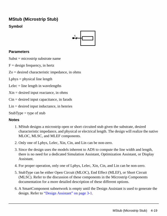
MStub (Microstrip Stub)
Symbol
Parameters
Subst = microstrip substrate name
F = design frequency, in hertz
Zo = desired characteristic impedance, in ohms
Lphys = physical line length
Lelec = line length in wavelengths
Xin = desired input reactance, in ohms
Cin = desired input capacitance, in farads
Lin = desired input inductance, in henries
StubType = type of stub
Notes
1. MStub designs a microstrip open or short circuited stub given the substrate, desiredcharacteristic impedance, and physical or electrical length. The design will realize the nMLOC, MLSC, and MLEF components.
2. Only one of Lphys, Lelec, Xin, Cin, and Lin can be non-zero.
3. Since the design uses the models inherent to ADS to compute the line width and lengthere is no need for a dedicated Simulation Assistant, Optimization Assistant, or DispAssistant.
4. For proper operation, only one of Lphys, Lelec, Xin, Cin, and Lin can be non-zero.
5. StubType can be either Open Circuit (MLOC), End Effect (MLEF), or Short Circuit(MLSC). Refer to the discussion of these components in the Microstrip Componentsdocumentation for a more detailed description of these different options.
6. A SmartComponent subnetwork is empty until the Design Assistant is used to generadesign. Refer to“Design Assistant” on page 3-1.
MStub (Microstrip Stub) 4-19
SmartComponent Reference
th,lay
r to thefor a
te the
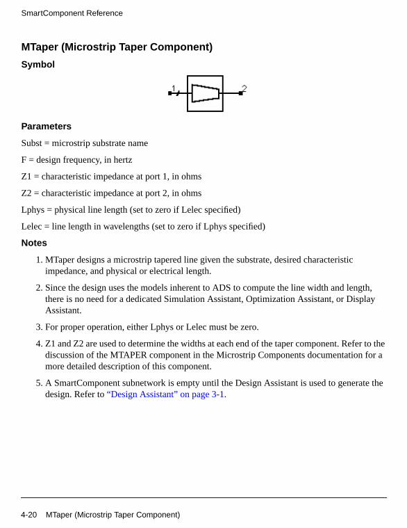
MTaper (Microstrip Taper Component)
Symbol
Parameters
Subst = microstrip substrate name
F = design frequency, in hertz
Z1 = characteristic impedance at port 1, in ohms
Z2 = characteristic impedance at port 2, in ohms
Lphys = physical line length (set to zero if Lelec specified)
Lelec = line length in wavelengths (set to zero if Lphys specified)
Notes
1. MTaper designs a microstrip tapered line given the substrate, desired characteristicimpedance, and physical or electrical length.
2. Since the design uses the models inherent to ADS to compute the line width and lengthere is no need for a dedicated Simulation Assistant, Optimization Assistant, or DispAssistant.
3. For proper operation, either Lphys or Lelec must be zero.
4. Z1 and Z2 are used to determine the widths at each end of the taper component. Refediscussion of the MTAPER component in the Microstrip Components documentation more detailed description of this component.
5. A SmartComponent subnetwork is empty until the Design Assistant is used to generadesign. Refer to“Design Assistant” on page 3-1.
4-20 MTaper (Microstrip Taper Component)

nce at
th,lay
of the
te the
MTee (Microstrip Tee Component)
Symbol
Parameters
Subst = microstrip substrate name
F = design frequency, in hertz
Z1 = characteristic impedance of port 1, in ohms
Z2 = characteristic impedance of port 2, in ohms
Z3 = characteristic impedance of port 3, in ohms
Notes
1. MTee designs a microstrip tee given the substrate and desired characteristic impedaeach port.
2. Since the design uses the models inherent to ADS to compute the line width and lengthere is no need for a dedicated Simulation Assistant, Optimization Assistant, or DispAssistant.
3. Z1, Z2, and Z3 are used to determine the widths of each port. Refer to the discussionMTEE component in the Microstrip Components documentation for a more detaileddescription of this component.
4. A SmartComponent subnetwork is empty until the Design Assistant is used to generadesign. Refer to“Design Assistant” on page 3-1.
MTee (Microstrip Tee Component) 4-21
SmartComponent Reference
al
oalG will length.
ake
the
Passive Circuit DG - RLC
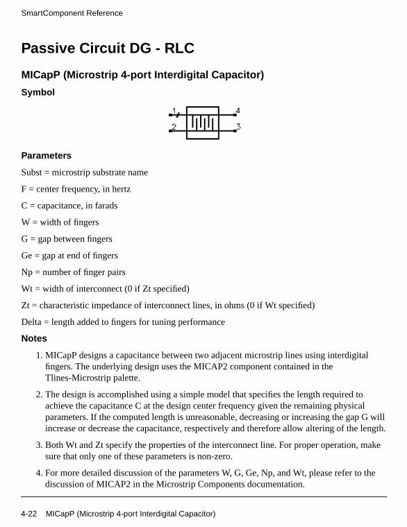
MICapP (Microstrip 4-port Interdigital Capacitor)
Symbol
Parameters
Subst = microstrip substrate name
F = center frequency, in hertz
C = capacitance, in farads
W = width of fingers
G = gap between fingers
Ge = gap at end of fingers
Np = number of finger pairs
Wt = width of interconnect (0 if Zt specified)
Zt = characteristic impedance of interconnect lines, in ohms (0 if Wt specified)
Delta = length added to fingers for tuning performance
Notes
1. MICapP designs a capacitance between two adjacent microstrip lines using interdigitfingers. The underlying design uses the MICAP2 component contained in theTlines-Microstrip palette.
2. The design is accomplished using a simple model that specifies the length required tachieve the capacitance C at the design center frequency given the remaining physicparameters. If the computed length is unreasonable, decreasing or increasing the gapincrease or decrease the capacitance, respectively and therefore allow altering of the
3. Both Wt and Zt specify the properties of the interconnect line. For proper operation, msure that only one of these parameters is non-zero.
4. For more detailed discussion of the parameters W, G, Ge, Np, and Wt, please refer todiscussion of MICAP2 in the Microstrip Components documentation.
4-22 MICapP (Microstrip 4-port Interdigital Capacitor)
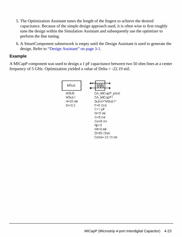
ghly
te the
ter
5. The Optimization Assistant tunes the length of the fingers to achieve the desiredcapacitance. Because of the simple design approach used, it is often wise to first routune the design within the Simulation Assistant and subsequently use the optimizer toperform the fine tuning.
6. A SmartComponent subnetwork is empty until the Design Assistant is used to generadesign. Refer to“Design Assistant” on page 3-1.
Example
A MICapP component was used to design a 1 pFcapacitance between two 50 ohm lines at a cenfrequency of 5 GHz. Optimization yielded a value of Delta = -22.19 mil.
MICapP (Microstrip 4-port Interdigital Capacitor) 4-23
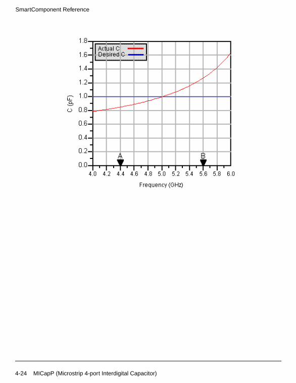
SmartComponent Reference
4-24 MICapP (Microstrip 4-port Interdigital Capacitor)
ital
oalG will length.
ake
the
ghly
MICapPG (Microstrip Grounded 2-port Interdigital Capacitor)
Symbol
Parameters
Subst = microstrip substrate name
F = center frequency, in hertz
C = capacitance, in farads
W = width of fingers
G = gap between fingers
Ge = gap at end of fingers
Wt = width of interconnect (0 if Zt specified)
Zt = characteristic impedance of interconnect lines, in ohms (0 if Wt specified)
Delta = length added to fingers for tuning performance
Notes
1. MICapPG designs a capacitance between a microstrip line and ground using interdigfingers. The underlying design uses the MICAP4 component contained in theTlines-Microstrip palette.
2. The design is accomplished using a simple model that specifies the length required tachieve the capacitance C at the design center frequency given the remaining physicparameters. If the computed length is unreasonable, decreasing or increasing the gapincrease or decrease the capacitance, respectively and therefore allow altering of the
3. Both Wt and Zt specify the properties of the interconnect line. For proper operation, msure that only one of these parameters is non-zero.
4. For more detailed discussion of the parameters W, G, Ge, Np, and Wt, please refer todiscussion of MICAP4 in the Microstrip Components documentation.
5. The Optimization Assistant tunes the length of the fingers to achieve the desiredcapacitance. Because of the simple design approach used, it is often wise to first rou
MICapPG (Microstrip Grounded 2-port Interdigital Capacitor) 4-25
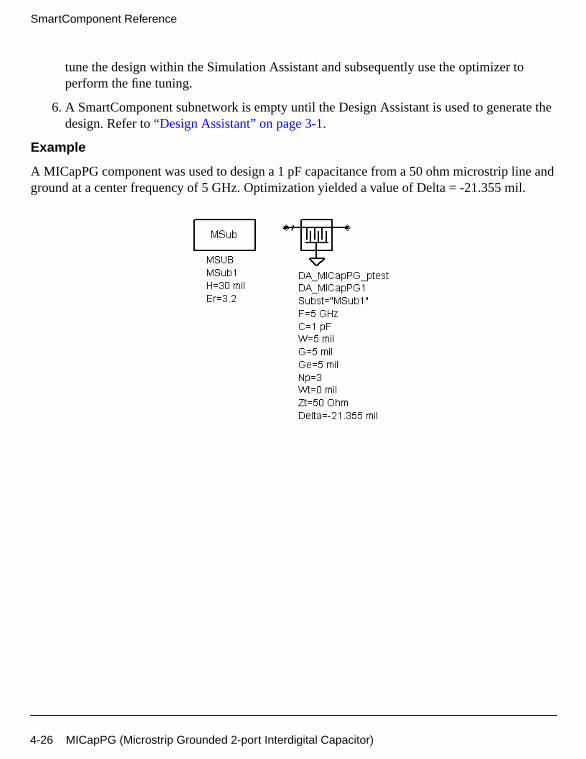
SmartComponent Reference
te the
d
tune the design within the Simulation Assistant and subsequently use the optimizer toperform the fine tuning.
6. A SmartComponent subnetwork is empty until the Design Assistant is used to generadesign. Refer to“Design Assistant” on page 3-1.
Example
A MICapPG component was used to design a 1 pFcapacitance from a 50 ohm microstrip line anground at a center frequency of 5 GHz. Optimization yielded a value of Delta = -21.355 mil.
4-26 MICapPG (Microstrip Grounded 2-port Interdigital Capacitor)
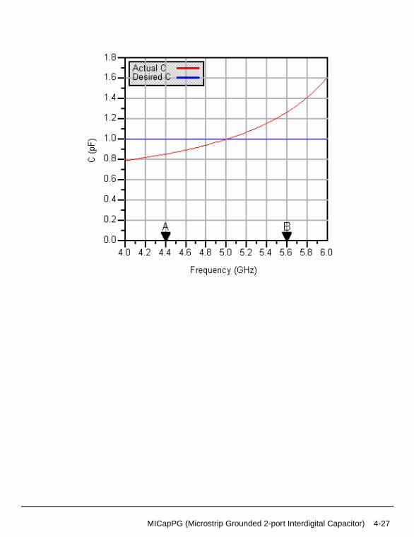
MICapPG (Microstrip Grounded 2-port Interdigital Capacitor) 4-27
SmartComponent Reference
. Thelette.
oalG will length.
that
fer to
ghly
MICapS (Microstrip 2-port Interdigital Capacitor)
Symbol
Parameters
Subst = microstrip substrate name
F = center frequency, in hertz
C = capacitance, in farads
W = width of fingers
G = gap between fingers
Ge = gap at end of fingers
Np = number of finger pairs
Wf = width of feed line (0 if Zf specified)
Zf = characteristic impedance of feed line, in ohms (0 if Wf specified)
Delta = length added to fingers for tuning performance
Notes
1. MICapS designs a series capacitance within a microstrip line using interdigital fingersunderlying design uses the MICAP1 component contained in the Tlines-Microstrip pa
2. The design is accomplished using a simple model that specifies the length required tachieve the capacitance C at the design center frequency given the remaining physicparameters. If the computed length is unreasonable, decreasing or increasing the gapincrease or decrease the capacitance, respectively and therefore allow altering of the
3. Both Wf and Zf specify the properties of the feed line. For proper operation, make sureonly one of these parameters is non-zero.
4. For more detailed discussion of the parameters W, G, Ge, Np, Wt, and Wf, please rethe discussion of MICAP1 in the Microstrip Components documentation.
5. The Optimization Assistant tunes the length of the fingers to achieve the desiredcapacitance. Because of the simple design approach used, it is often wise to first rou
4-28 MICapS (Microstrip 2-port Interdigital Capacitor)
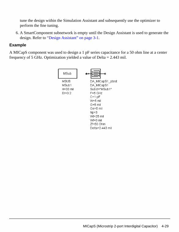
te the
center
tune the design within the Simulation Assistant and subsequently use the optimizer toperform the fine tuning.
6. A SmartComponent subnetwork is empty until the Design Assistant is used to generadesign. Refer to“Design Assistant” on page 3-1.
Example
A MICapS component was used to design a 1 pF series capacitance for a 50 ohm line at afrequency of 5 GHz. Optimization yielded a value of Delta = 2.443 mil.
MICapS (Microstrip 2-port Interdigital Capacitor) 4-29
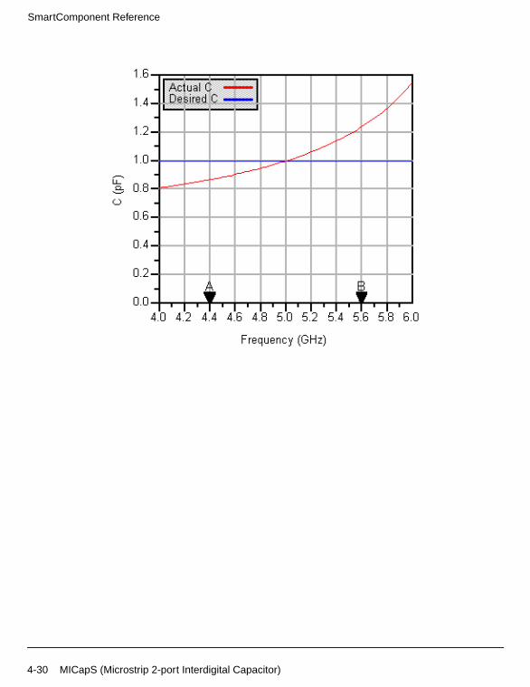
SmartComponent Reference
4-30 MICapS (Microstrip 2-port Interdigital Capacitor)
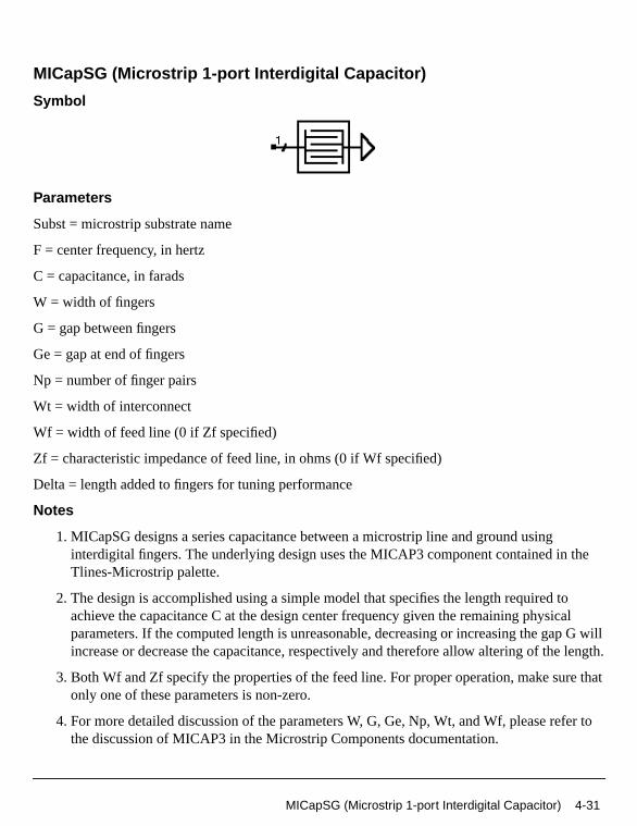
the
oalG will length.
that
fer to
MICapSG (Microstrip 1-port Interdigital Capacitor)
Symbol
Parameters
Subst = microstrip substrate name
F = center frequency, in hertz
C = capacitance, in farads
W = width of fingers
G = gap between fingers
Ge = gap at end of fingers
Np = number of finger pairs
Wt = width of interconnect
Wf = width of feed line (0 if Zf specified)
Zf = characteristic impedance of feed line, in ohms (0 if Wf specified)
Delta = length added to fingers for tuning performance
Notes
1. MICapSG designs a series capacitance between a microstrip line and ground usinginterdigital fingers. The underlying design uses the MICAP3 component contained in Tlines-Microstrip palette.
2. The design is accomplished using a simple model that specifies the length required tachieve the capacitance C at the design center frequency given the remaining physicparameters. If the computed length is unreasonable, decreasing or increasing the gapincrease or decrease the capacitance, respectively and therefore allow altering of the
3. Both Wf and Zf specify the properties of the feed line. For proper operation, make sureonly one of these parameters is non-zero.
4. For more detailed discussion of the parameters W, G, Ge, Np, Wt, and Wf, please rethe discussion of MICAP3 in the Microstrip Components documentation.
MICapSG (Microstrip 1-port Interdigital Capacitor) 4-31
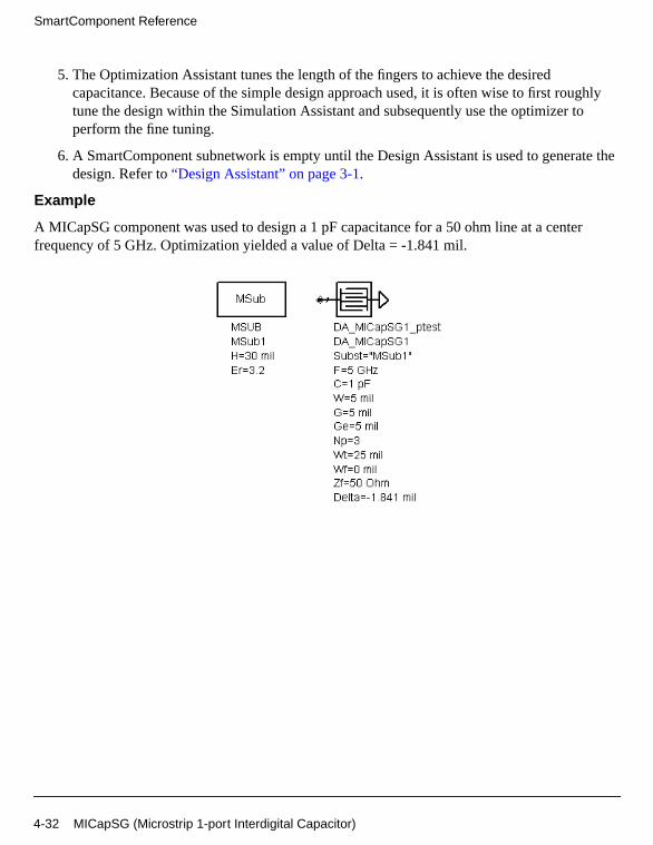
SmartComponent Reference
ghly
te the
er
5. The Optimization Assistant tunes the length of the fingers to achieve the desiredcapacitance. Because of the simple design approach used, it is often wise to first routune the design within the Simulation Assistant and subsequently use the optimizer toperform the fine tuning.
6. A SmartComponent subnetwork is empty until the Design Assistant is used to generadesign. Refer to“Design Assistant” on page 3-1.
Example
A MICapSG component was used to design a 1 pF capacitance for a 50 ohm line at a centfrequency of 5 GHz. Optimization yielded a value of Delta = -1.841 mil.
4-32 MICapSG (Microstrip 1-port Interdigital Capacitor)
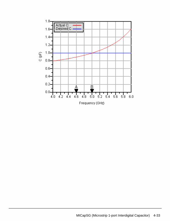
MICapSG (Microstrip 1-port Interdigital Capacitor) 4-33
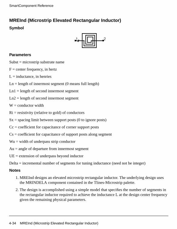
SmartComponent Reference
ses
ents inuency
MREInd (Microstrip Elevated Rectangular Inductor)
Symbol
Parameters
Subst = microstrip substrate name
F = center frequency, in hertz
L = inductance, in henries
Ln = length of innermost segment (0 means full length)
Ln1 = length of second innermost segment
Ln2 = length of second innermost segment
W = conductor width
Ri = resistivity (relative to gold) of conductors
Sx = spacing limit between support posts (0 to ignore posts)
Cc = coefficient for capacitance of corner support posts
Cs = coefficient for capacitance of support posts along segment
Wu = width of underpass strip conductor
Au = angle of departure from innermost segment
UE = extension of underpass beyond inductor
Delta = incremental number of segments for tuning inductance (need not be integer)
Notes
1. MREInd designs an elevated microstrip rectangular inductor. The underlying design uthe MRINDELA component contained in the Tlines-Microstrip palette.
2. The design is accomplished using a simple model that specifies the number of segmthe rectangular inductor required to achieve the inductance L at the design center freqgiven the remaining physical parameters.
4-34 MREInd (Microstrip Elevated Rectangular Inductor)

theot be
h the
eed
te the
The
red
3. The parameters from Hi through Cs are not actually used in the design process, andtherefore final tuning is required to achieve the proper value of the inductance.
4. The tuning parameter Delta represents the number of additional segments to add to outside of the structure. If it is not an integer value, the outermost segment (L1) will nfull length, with the fractional remainder of Delta specifying the fractional length of thisoutermost segment.
5. The values Ln, Ln1, and Ln2 represent the lengths Ln, Ln-1, and Ln-2 associated witMRINDELA component. For more detailed discussion of these lengths as well as theparameters from W through UE, please refer to the discussion of MRINDELA in theMicrostrip Components documentation.
6. Because of the difficulties associated with tuning the inductor using additional discretsegments, no Optimization Assistant is provided. However, tuning can be accomplishquite effectively by manually updating the value of Delta from within the SimulationAssistant. Refer to“Optimization Assistant” on page 3-4, as well as the following examplefor more details.
7. A SmartComponent subnetwork is empty until the Design Assistant is used to generadesign. Refer to“Design Assistant” on page 3-1.
Example
A MREInd component was used to design a 1 nH inductor at a center frequency of 3 GHz. design used a full-length innermost segment. By tuning the number of segments within theSimulation Assistant, it was determined that a value of Delta = 1.63 would achieve the desiinductance.
MREInd (Microstrip Elevated Rectangular Inductor) 4-35
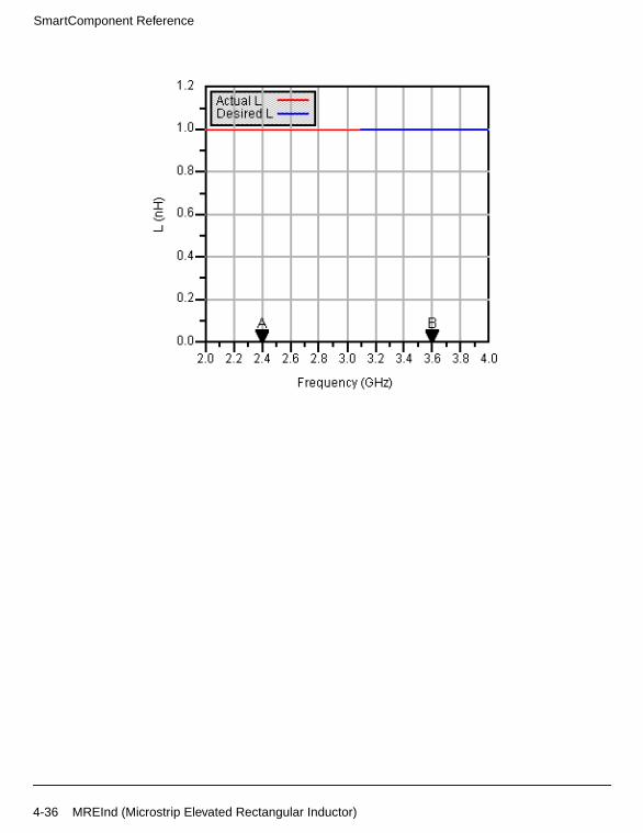
SmartComponent Reference
4-36 MREInd (Microstrip Elevated Rectangular Inductor)
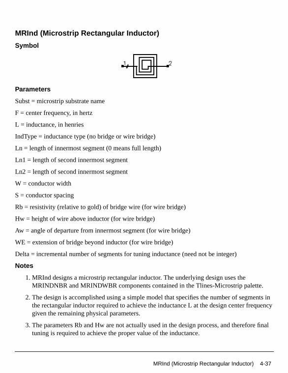
ents inuency
e final
MRInd (Microstrip Rectangular Inductor)
Symbol
Parameters
Subst = microstrip substrate name
F = center frequency, in hertz
L = inductance, in henries
IndType = inductance type (no bridge or wire bridge)
Ln = length of innermost segment (0 means full length)
Ln1 = length of second innermost segment
Ln2 = length of second innermost segment
W = conductor width
S = conductor spacing
Rb = resistivity (relative to gold) of bridge wire (for wire bridge)
Hw = height of wire above inductor (for wire bridge)
Aw = angle of departure from innermost segment (for wire bridge)
WE = extension of bridge beyond inductor (for wire bridge)
Delta = incremental number of segments for tuning inductance (need not be integer)
Notes
1. MRInd designs a microstrip rectangular inductor. The underlying design uses theMRINDNBR and MRINDWBR components contained in the Tlines-Microstrip palette.
2. The design is accomplished using a simple model that specifies the number of segmthe rectangular inductor required to achieve the inductance L at the design center freqgiven the remaining physical parameters.
3. The parameters Rb and Hw are not actually used in the design process, and therefortuning is required to achieve the proper value of the inductance.
MRInd (Microstrip Rectangular Inductor) 4-37

SmartComponent Reference
ter isfrom
theot be
h thegthsonents
eed
te the
y of 3 withinsired
4. The value of IndType specifies the type of inductor that will be designed. If this parameset to “No Bridge”, then the MRINDNBR component is designed and the parameters Dw to WE are ignored. If the parameter is set to “Wire Bridge”, then the MRINDWBRcomponent is designed and the parameters from Dw to WE are used.
5. The tuning parameter Delta represents the number of additional segments to add to outside of the structure. If it is not an integer value, the outermost segment (L1) will nfull length, with the fractional remainder of Delta specifying the fractional length of thisoutermost segment.
6. The values Ln, Ln1, and Ln2 represent the lengths Ln, Ln-1, and Ln-2 associated witMRINDNBR and MRINDWBR components. For more detailed discussion of these lenas well as the parameters W through WE, please refer to the discussion of these compin the Microstrip Components documentation.
7. Because of the difficulties associated with tuning the inductor using additional discretsegments, no Optimization Assistant is provided. However, tuning can be accomplishquite effectively by manually updating the value of Delta from within the SimulationAssistant, refer to“Optimization Assistant” on page 3-4, as well as the following examplefor more details.
8. A SmartComponent subnetwork is empty until the Design Assistant is used to generadesign. Refer to“Design Assistant” on page 3-1.
Example
A MRInd component with no bridge was used to design a 1 nH inductor at a center frequencGHz. The design used a full-length innermost segment. By tuning the number of segmentsthe Simulation Assistant, it was determined that a value of Delta = 0.52 would achieve the deinductance.
4-38 MRInd (Microstrip Rectangular Inductor)
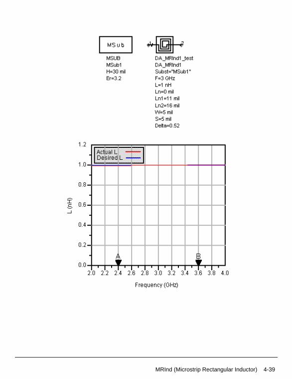
MRInd (Microstrip Rectangular Inductor) 4-39

SmartComponent Reference
in then the
the
on of
utsidee an
ce.
te the
MSInd (Microstrip Spiral Inductor)
Symbol
Parameters
Subst = microstrip substrate name
F = center frequency, in hertz
Ri = inner radius measured to center of conductor
W = conductor width
S = conductor spacing
W1 = width of strip connected to pin 1
W2 = width of strip connected to pin 2
Delta = incremental number of turns for tuning inductance (need not be integer)
Notes
1. MSInd designs a microstrip spiral inductor. The underlying design uses the MSINDcomponent contained in the Tlines-Microstrip palette.
2. The design is accomplished using a simple model that specifies the number of turns spiral inductor required to achieve the inductance L at the design center frequency giveremaining physical parameters.
3. The value of Ri specifies the distance from the center of the inductor to the center of conductor at its innermost point in the spiral. Refer to the discussion of the MSINDcomponent in the Microstrip Components documentation for a more detailed discussithis parameter.
4. The tuning parameter Delta represents the number of additional turns to add to the oof the structure. Fractional numbers of turns are accommodated (i.e. Delta need not binteger value).
5. The Optimization Assistant tunes the number of turns to achieve the desired inductan
6. A SmartComponent subnetwork is empty until the Design Assistant is used to generadesign. Refer to“Design Assistant” on page 3-1.
4-40 MSInd (Microstrip Spiral Inductor)
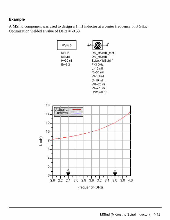
Example
A MSInd component was used to design a 1 nH inductor at a center frequency of 3 GHz.Optimization yielded a value of Delta = -0.53.
MSInd (Microstrip Spiral Inductor) 4-41

SmartComponent Reference
dified
MTFC (Microstrip Thin Film Capacitor)
Symbol
Parameters
Subst = microstrip substrate name
F = center frequency, in hertz
C = capacitance, in farads
W = conductor width (set to 0 if Zo specified)
Zo = characteristic impedance of line for computing W (set to 0 if W specified)
CPUA = capacitance per unit area, in pf/mm^2
T = thickness of capacitor dielectric
RsT = sheet resistance of top metal plate, in ohms
RsB = sheet resistance of bottom metal plate, in ohms
TT = thickness of top metal plate
TB = thickness of bottom metal plate
COB= bottom conductor overlap
COT = top conductor overlap
DO = dielectric overlap
Delta = length added to conductor for tuning capacitance
Notes
1. MTFC designs a microstrip thin film capacitor. The underlying design uses the MTFCcomponent contained in the Tlines-Microstrip palette.
2. The design is accomplished by determining the length required to achieve the desirecapacitance using the capacitance per unit area (CPUA) in conjunction with the specwidth (W).
4-42 MTFC (Microstrip Thin Film Capacitor)
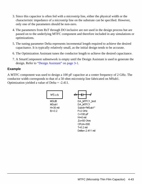
ver,
ut arens or
sired
ance.
te the
. The
3. Since this capacitor is often fed with a microstrip line, either the physical width or thecharacteristic impedance of a microstrip line on the substrate can be specified. Howeonly one of the parameters should be non-zero.
4. The parameters from RsT through DO inclusive are not used in the design process bpassed on to the underlying MTFC component and therefore included in any simulatiooptimizations.
5. The tuning parameter Delta represents incremental length required to achieve the decapacitance. It is typically relatively small, as the initial design tends to be accurate.
6. The Optimization Assistant tunes the conductor length to achieve the desired capacit
7. A SmartComponent subnetwork is empty until the Design Assistant is used to generadesign. Refer to“Design Assistant” on page 3-1.
Example
A MTFC component was used to design a 100 pF capacitor at a center frequency of 2 GHzconductor width corresponds to that of a 50 ohm microstrip line fabricated on MSub1.Optimization yielded a value of Delta = -2.411.
MTFC (Microstrip Thin Film Capacitor) 4-43
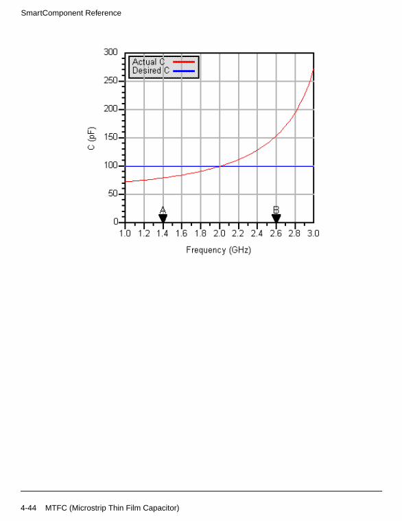
SmartComponent Reference
4-44 MTFC (Microstrip Thin Film Capacitor)
d
to thetions.
sired
ance.
te the
TFC (Thin Film Capacitor)
Symbol
Parameters
F = center frequency, in hertz
C = capacitance, in farads
W = conductor width
T = thickness of capacitor dielectric
Er = relative dielectric constant
Rho = resistivity of conductor (relative to gold)
TanD = dielectric loss tangent
CO = conductor overlap
DO = dielectric overlap
Delta = length added to conductor for tuning capacitance
Notes
1. TFC designs a thin film capacitor. The underlying design uses the TFC componentcontained in the Tlines-Microstrip palette.
2. The design is accomplished by determining the length required to achieve the desirecapacitance using the simple parallel plate capacitor model C = Er*W*L/T. The parametersfrom Rho through DO inclusive are not used in the design process but are passed onunderlying TFC component and are therefore included in any simulations or optimiza
3. The tuning parameter Delta represents incremental length required to achieve the decapacitance. It is typically relatively small, as the initial design tends to be accurate.
4. The Optimization Assistant tunes the conductor length to achieve the desired capacit
5. A SmartComponent subnetwork is empty until the Design Assistant is used to generadesign. Refer to“Design Assistant” on page 3-1.
TFC (Thin Film Capacitor) 4-45
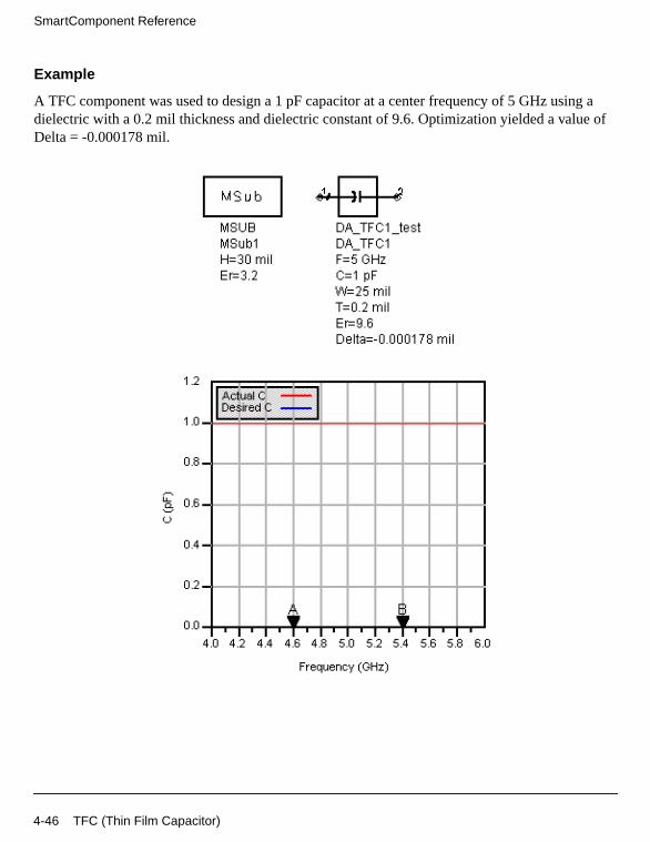
SmartComponent Reference
g ae of
Example
A TFC component was used to design a 1 pF capacitor at a center frequency of 5 GHz usindielectric with a 0.2 mil thickness and dielectric constant of 9.6. Optimization yielded a valuDelta = -0.000178 mil.
4-46 TFC (Thin Film Capacitor)

tained
d
tions.
sired
ce.
te the
TFR (Thin Film Resistor)
Symbol
Parameters
Subst = microstrip substrate name
F = center frequency, in hertz
R = resistance, in ohms
W = conductor width (set to 0 if Zo specified)
Zo = characteristic impedance of line assuming Rs = 0 (set to 0 if W specified)
Rs = sheet resistivity, in ohms/square
CO = conductor overlap
Delta = length added to conductor for tuning resistance
Notes
1. TFR designs a thin film resistor. The underlying design uses the TFR component conin the Tlines-Microstrip palette.
2. The design is accomplished by determining the length required to achieve the desireresistance using the sheet resistivity Rs in conjunction with the strip width W. Theparameters Freq and CO are not used in the design process but are passed on to theunderlying TFR component and are therefore included in any simulations or optimiza
3. Since this resistor is often fed with a microstrip line, either the physical width or thecharacteristic impedance of a microstrip line on the substrate can be specified.
4. The tuning parameter Delta represents incremental length required to achieve the deresistance.
5. The Optimization Assistant tunes the conductor length to achieve the desired resistan
6. A SmartComponent subnetwork is empty until the Design Assistant is used to generadesign. Refer to“Design Assistant” on page 3-1.
TFR (Thin Film Resistor) 4-47
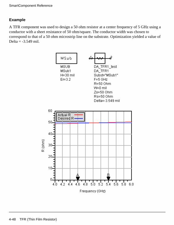
SmartComponent Reference
ing a
e of
Example
A TFR component was used to design a 50 ohm resistor at a center frequency of 5 GHz usconductor with a sheet resistance of 50 ohm/square. The conductor width was chosen tocorrespond to that of a 50 ohm microstrip line on the substrate. Optimization yielded a valuDelta = -3.549 mil.
4-48 TFR (Thin Film Resistor)

utputgrees,
input
ineder,3 dB
Passive Circuit DG - Couplers
BLCoupler (Branch-Line Coupler)
Symbol
Parameters
Subst = microstrip substrate name
F = center frequency, in hertz
DeltaF = total frequency bandwidth, in hertz
Zo = characteristic impedance, in ohms
ResponseType = type of frequency response
N = number of coupler sections (set N = 0 to compute N)
Rmax = maximum voltage reflection coefficient at the input
C = coupling coefficient, in dB
Delta = length added to branches for tuning performance
Notes
1. A branch-line coupler outputs from the coupled port (pin 3) a fraction of the powerpresented at the input (pin 1). The remainder of the power is passed through to the oport (pin 2). At the center frequency the phase difference between the outputs is 90 dewith the coupled port representing the quadrature (Q) output and the output portrepresenting the in-phase (I) output. The coupling coefficient specifies the ratio of thepower to the coupled power (P1/P3). Pin 4 represents the isolated port, and it is typically
well isolated from the input port near the center frequency.
2. The coupling coefficient must be positive and greater than 3 dB. Best results are obtafor tight couplings of 6 dB or better (C < 6 dB). Choosing the coupling parameter largthan 6 dB often causes width constraint violations to occur on the MTEE componentsresulting in warning messages during design and simulation. A coupling coefficient ofprovides an equal power split between the two outputs.
BLCoupler (Branch-Line Coupler) 4-49
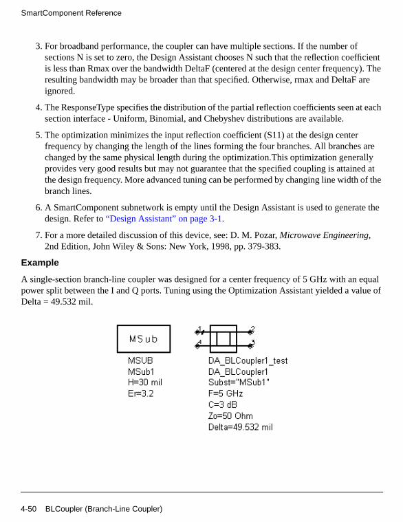
SmartComponent Reference
fficient). Theare
t each
areallyed atof the
te the
equalue of
3. For broadband performance, the coupler can have multiple sections. If the number ofsections N is set to zero, the Design Assistant chooses N such that the reflection coeis less than Rmax over the bandwidth DeltaF (centered at the design center frequencyresulting bandwidth may be broader than that specified. Otherwise, rmax and DeltaF ignored.
4. The ResponseType specifies the distribution of the partial reflection coefficients seen asection interface - Uniform, Binomial, and Chebyshev distributions are available.
5. The optimization minimizes the input reflection coefficient (S11) at the design centerfrequency by changing the length of the lines forming the four branches. All brancheschanged by the same physical length during the optimization.This optimization generprovides very good results but may not guarantee that the specified coupling is attainthe design frequency. More advanced tuning can be performed by changing line widthbranch lines.
6. A SmartComponent subnetwork is empty until the Design Assistant is used to generadesign. Refer to“Design Assistant” on page 3-1.
7. For a more detailed discussion of this device, see: D. M. Pozar,Microwave Engineering,2nd Edition, John Wiley & Sons: New York, 1998, pp. 379-383.
Example
A single-section branch-line coupler was designed for a center frequency of 5 GHz with anpower split between the I and Q ports. Tuning using the Optimization Assistant yielded a valDelta = 49.532 mil.
4-50 BLCoupler (Branch-Line Coupler)
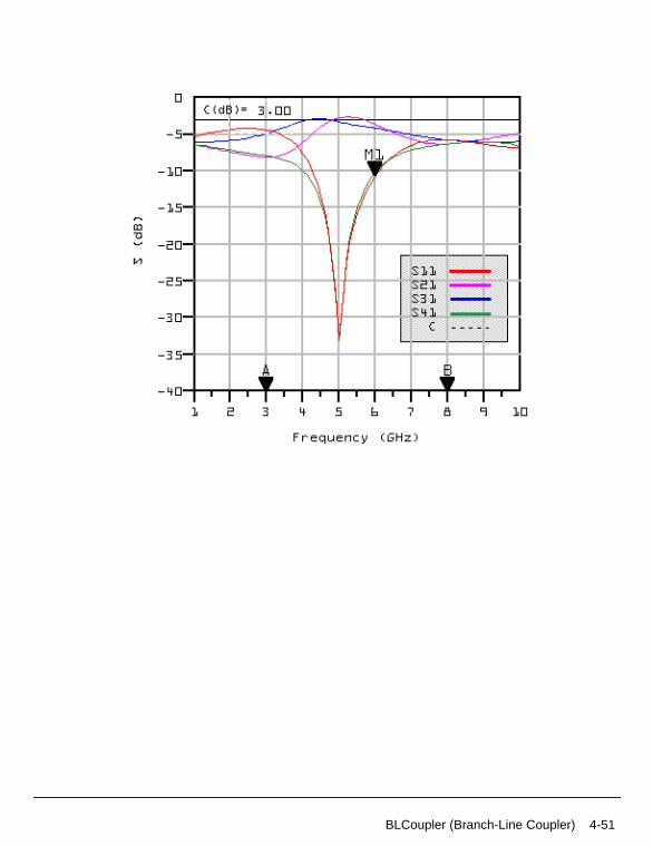
BLCoupler (Branch-Line Coupler) 4-51

SmartComponent Reference
utputledlue
fied
inedient
te the
CLCoupler (Coupled-Line Coupler)
Symbol
Parameters
Subst = microstrip substrate name
F = center frequency, in hertz
C = coupling coefficient, in dB
Zo = characteristic impedance, in ohms
Delta = length added to branches for tuning performance
Notes
1. A coupled-line coupler outputs from the coupled port (pin 4) a fraction of the powerpresented at the input (pin 1). The remainder of the power is passed through to the oport (pin 2). The coupling coefficient specifies the ratio of the input power to the couppower (P1/P4). The remaining port is isolated, although the isolation is often similar in va
to the coupling coefficient for microstrip realizations.
2. The optimization minimizes the absolute difference between S41 in dB and the specicoupling coefficient at the design center frequency by changing the length of thecoupled-line section.
3. The coupling coefficient must be positive and greater than 3 dB. Best results are obtafor weak couplings of roughly 10 dB or more (C >10dB). Choosing the coupling coeffictoo small may require a spacing between the coupled lines too small to realize.
4. A SmartComponent subnetwork is empty until the Design Assistant is used to generadesign. Refer to“Design Assistant” on page 3-1.
5. For a more detailed discussion of this device, see: D. M. Pozar,Microwave Engineering,2nd Edition, John Wiley & Sons: New York, 1998, pp. 383-394.
4-52 CLCoupler (Coupled-Line Coupler)
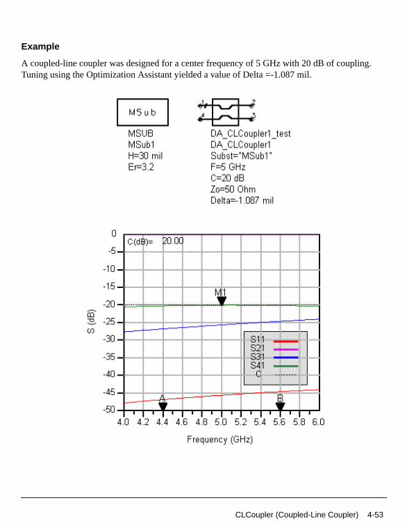
g.
Example
A coupled-line coupler was designed for a center frequency of 5 GHz with 20 dB of couplinTuning using the Optimization Assistant yielded a value of Delta =-1.087 mil.
CLCoupler (Coupled-Line Coupler) 4-53

SmartComponent Reference
t (pinifies
e
ieve theers is
plingn.
te the
LCoupler (Lange Coupler)
Symbol
Parameters
Subst = microstrip substrate name
F = center frequency, in hertz
C = coupling coefficient, in dB
N = number of fingers (4, 6, or 8)
Zo = characteristic impedance, in ohms
Delta = length added to fingers for tuning performance
Notes
1. A Lange coupler outputs from pin 2 a small fraction of the power presented at the inpu1). The remainder of the power is passed through pin 3. The coupling coefficient specthe power ratio P1/P2. Pin 4 is isolated, and often the isolation is 10 dB better than the
coupling coefficient in microstrip realizations.
2. The Lange coupler is best for weak couplings of roughly 10 dB or more (C >10dB).Choosing the coupling coefficient too small may produce an unrealizable design. If thdesign creates a finger spacing S that is not realizable, increase the value of N.
3. The Design Assistant computes the required even and odd mode impedances to achdesired coupling and translates them to finger width and spacing. The length of the finga quarter wavelength at the design frequency.
4. The optimization minimizes the absolute difference between S21 and the specified coucoefficient at the design center frequency by changing the length of the fingers sectio
5. A SmartComponent subnetwork is empty until the Design Assistant is used to generadesign. Refer to“Design Assistant” on page 3-1.
6. For a more detailed discussion of this device, see: I. Bahl and P. Bhartia,Microwave SolidState Circuit Design, John Wiley & Sons: New York, 1988, pp. 209-211.
4-54 LCoupler (Lange Coupler)
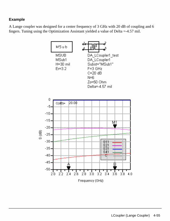
6
Example
A Lange coupler was designed for a center frequency of 3 GHz with 20 dB of coupling andfingers. Tuning using the Optimization Assistant yielded a value of Delta =-4.57 mil.
LCoupler (Lange Coupler) 4-55

SmartComponent Reference
enal isTheetimes
rts are
sign
te the
2 GHz.
RRCoupler (Rat-Race Coupler)
Symbol
Parameters
Subst = microstrip substrate name
F = center frequency, in hertz
Zo = characteristic impedance, in ohms
Delta = length added to ring branches for tuning
Notes
1. A rat-race coupler equally divides the power input at port 1 between ports 2 and 3. Thsignal at the output ports 2 and 3 are in-phase. Port 4 is isolated from port 1. If the sigdriven from port 2, then the power is divided between ports 1 and 4 with port 3 isolated.signal at ports 1 and 4 are 180 degrees out of phase, and therefore this device is somreferred to as a 180-degree hybrid.
2. The design specifies the width and length of the microstrip lines to ensure that the pomatched to Zo and equal power split is achieved at the design center frequency.
3. The optimization minimizes the value of S11 (referenced to the value of Zo) at the decenter frequency by changing the length of the ring.
4. A SmartComponent subnetwork is empty until the Design Assistant is used to generadesign. Refer to“Design Assistant” on page 3-1.
5. For a more detailed discussion of this device, see: D. M. Pozar,Microwave Engineering,2nd Edition, John Wiley & Sons: New York, 1998, pp. 401-407.
Example
A rat-race coupler was designed for a 50 ohm system impedance at a center frequency of Tuning using the Optimization Assistant yielded a value of Delta =-2.099 mil.
4-56 RRCoupler (Rat-Race Coupler)
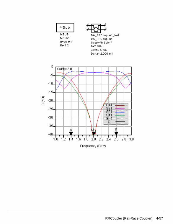
RRCoupler (Rat-Race Coupler) 4-57

SmartComponent Reference
ands
ever,hs oftion
power
.
te the
TCoupler (Tee Power Divider)
Symbol
Parameters
Subst = microstrip substrate name
F = center frequency, in hertz
Zo1 = characteristic impedance of input port 1, in ohms
Zo2 = characteristic impedance of output port 2, in ohms
K = ratio of power out port 2 to power out port 3
Delta = length added to quarter-wave sections for tuning performance
Notes
1. A tee power divider splits the power at the input (pin 1) between the two outputs (pins 23). Unequal or equal power splits can be realized. The input port will be matched to itfeeding line, although in general the output ports will not be matched.
2. The value of K can be set to realize the desired power split out of ports 2 and 3. Howchoosing K larger than 3 to 4 (or smaller than 1/3 to 1/4) may cause the ratio of the widtthe tee branches to violate the range of the MTEE simulation model. While the simulawill still proceed, the results may have some inaccuracies.
3. Quarter-wave matching sections are provided on the output ports to ensure a proper split is achieved.
4. The optimization minimizes the input reflection coefficient (S11) at the design centerfrequency by changing the length of the quarter wave transformers on the output legs
5. A SmartComponent subnetwork is empty until the Design Assistant is used to generadesign. Refer to“Design Assistant” on page 3-1.
6. For a more detailed discussion of this device, see: D. M. Pozar,Microwave Engineering,2nd Edition, John Wiley & Sons: New York, 1998, pp. 360-361.
4-58 TCoupler (Tee Power Divider)
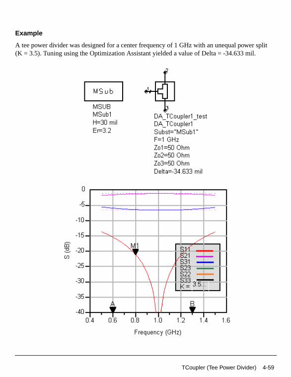
plit
Example
A tee power divider was designed for a center frequency of 1 GHz with an unequal power s(K = 3.5). Tuning using the Optimization Assistant yielded a value of Delta = -34.633 mil.
TCoupler (Tee Power Divider) 4-59
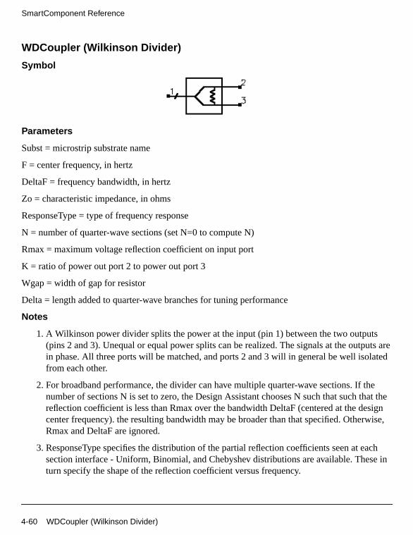
SmartComponent Reference
tsuts areated
hehat thesignwise,
ache in
WDCoupler (Wilkinson Divider)
Symbol
Parameters
Subst = microstrip substrate name
F = center frequency, in hertz
DeltaF = frequency bandwidth, in hertz
Zo = characteristic impedance, in ohms
ResponseType = type of frequency response
N = number of quarter-wave sections (set N=0 to compute N)
Rmax = maximum voltage reflection coefficient on input port
K = ratio of power out port 2 to power out port 3
Wgap = width of gap for resistor
Delta = length added to quarter-wave branches for tuning performance
Notes
1. A Wilkinson power divider splits the power at the input (pin 1) between the two outpu(pins 2 and 3). Unequal or equal power splits can be realized. The signals at the outpin phase. All three ports will be matched, and ports 2 and 3 will in general be well isolfrom each other.
2. For broadband performance, the divider can have multiple quarter-wave sections. If tnumber of sections N is set to zero, the Design Assistant chooses N such that such treflection coefficient is less than Rmax over the bandwidth DeltaF (centered at the decenter frequency). the resulting bandwidth may be broader than that specified. OtherRmax and DeltaF are ignored.
3. ResponseType specifies the distribution of the partial reflection coefficients seen at esection interface - Uniform, Binomial, and Chebyshev distributions are available. Thesturn specify the shape of the reflection coefficient versus frequency.
4-60 WDCoupler (Wilkinson Divider)
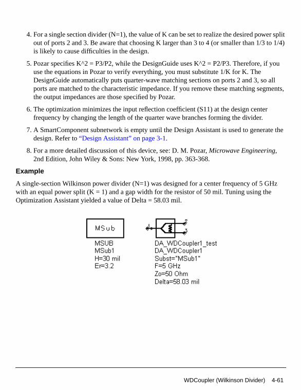
r split1/4)
you
allments,
te the
Hz
4. For a single section divider (N=1), the value of K can be set to realize the desired poweout of ports 2 and 3. Be aware that choosing K larger than 3 to 4 (or smaller than 1/3 tois likely to cause difficulties in the design.
5. Pozar specifies K^2 = P3/P2, while the DesignGuide uses K^2 = P2/P3. Therefore, ifuse the equations in Pozar to verify everything, you must substitute 1/K for K. TheDesignGuide automatically puts quarter-wave matching sections on ports 2 and 3, soports are matched to the characteristic impedance. If you remove these matching segthe output impedances are those specified by Pozar.
6. The optimization minimizes the input reflection coefficient (S11) at the design centerfrequency by changing the length of the quarter wave branches forming the divider.
7. A SmartComponent subnetwork is empty until the Design Assistant is used to generadesign. Refer to“Design Assistant” on page 3-1.
8. For a more detailed discussion of this device, see: D. M. Pozar,Microwave Engineering,2nd Edition, John Wiley & Sons: New York, 1998, pp. 363-368.
Example
A single-section Wilkinson power divider (N=1) was designed for a center frequency of 5 Gwith an equal power split (K = 1) and a gap width for the resistor of 50 mil. Tuning using theOptimization Assistant yielded a value of Delta = 58.03 mil.
WDCoupler (Wilkinson Divider) 4-61
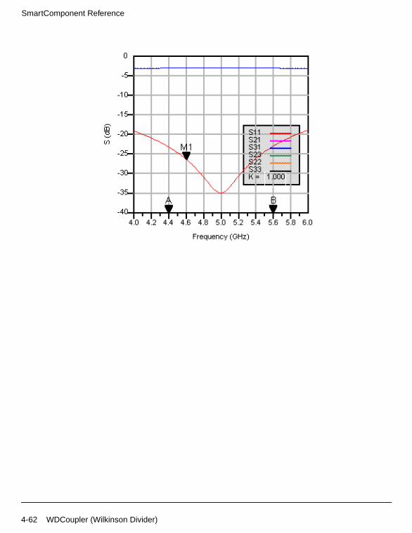
SmartComponent Reference
4-62 WDCoupler (Wilkinson Divider)
outputrs of
dth.
delay
dB arend
Passive Circuit DG - Filters
CLFilter (Coupled-Line Filter)
Symbol
Parameters
Subst = microstrip substrate name
Fs1 = lower stopband edge frequency, in hertz
Fp1 = lower passband edge frequency, in hertz
Fp2 = upper passband edge frequency, in hertz
Fs2 = lower stopband edge frequency, in hertz
Ap = passband edge attenuation (or ripple for Chebyshev), in dB
As = stopband edge attenuation, in dB
N = number of filter sections (or 0 to compute N)
ResponseType = type of frequency response (maximally flat or Chebyshev)
Zo = desired input/output impedance, in ohms
Delta = length added to coupled sections for tuning performance
Notes
1. A coupled-line filter provides a bandpass frequency response between the input and ports. N coupled-line sections produces an N-1 order filter response. Additional numbesections can be used to steepen the transition band roll off or widen the pass bandwi
2. Because of the heavy computational burden in determining the line parameters, a briefwill occur for the design.
3. For a Chebyshev (equal ripple) frequency response, ripple levels greater than about 1not recommended. Exceeding this value will typically deform the shape of the passbacharacteristics.
CLFilter (Coupled-Line Filter) 4-63
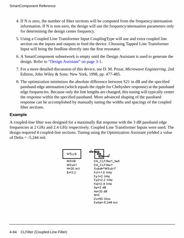
SmartComponent Reference
tiononly
mer
te the
fiedssbandenter
upled
ge. The
value
4. If N is zero, the number of filter sections will be computed from the frequency/attenuainformation. If N is non-zero, the design will use the frequency/attenuation parametersfor determining the design center frequency.
5. Using a Coupled Line Transformer Input CouplingType will use and extra coupled linesection on the inputs and outputs to feed the device. Choosing Tapped Line TransforInput will bring the feedline directly into the first resonator.
6. A SmartComponent subnetwork is empty until the Design Assistant is used to generadesign. Refer to“Design Assistant” on page 3-1.
7. For a more detailed discussion of this device, see D. M. Pozar,Microwave Engineering, 2ndEdition, John Wiley & Sons: New York, 1998, pp. 477-485.
8. The optimization minimizes the absolute difference between S21 in dB and the specipassband edge attenuation (which equals the ripple for Chebyshev response) at the paedge frequencies. Because only the line lengths are changed, this tuning will typically cthe response within the specified passband. More advanced shaping of the passbandresponse can be accomplished by manually tuning the widths and spacings of the cofilter sections.
Example
A coupled-line filter was designed for a maximally flat response with the 3 dB passband edfrequencies at 2 GHz and 2.4 GHz respectively. Coupled Line Transformer Inputs were useddesign required 4 coupled-line sections. Tuning using the Optimization Assistant yielded a of Delta = -5.244 mil.
4-64 CLFilter (Coupled-Line Filter)
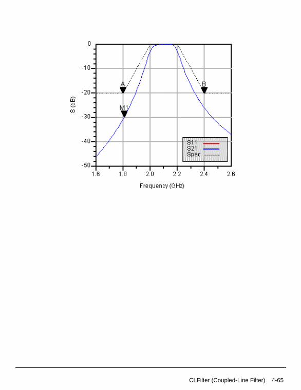
CLFilter (Coupled-Line Filter) 4-65

SmartComponent Reference
gth
tputrs of
dth.
delay
CMFilter (Comb-Line Filter)
Symbol
Parameters
Subst = microstrip substrate name
Fs1 = lower stopband edge frequency, in hertz
Fp1 = lower passband edge frequency, in hertz
Fp2 = upper passband edge frequency, in hertz
Fs2 = lower stopband edge frequency, in hertz
Ap = passband edge attenuation (or ripple for Chebyshev), in dB
As = stopband edge attenuation, in dB
N = number of filter sections (or 0 to compute N)
ResponseType = type of frequency response (maximally flat or Chebyshev)
Zo = desired input/output impedance, in ohms
Lelec = electrical length of filter resonators (the units of Leclec are in fractions of a waveleni.e., 0.25 = 1/4 wavelength)
ya = normalized interior resonator admittance (0 < ya < 1)
CouplingType = type of input/output coupling (coupled line or tapped line transformer)
Delta = length added to coupled sections for tuning performance
Notes
1. A comb-line filter provides a bandpass frequency response between the input and ouports. N coupled-line sections produce an N-1 order filter response. Additional numbesections can be used to steepen the transition band roll off or widen the pass bandwi
2. Because of the heavy computational burden in determining the line parameters, a briefwill occur for the design.
3. A two-layer substrate must be used for this topology.
4-66 CMFilter (Comb-Line Filter)
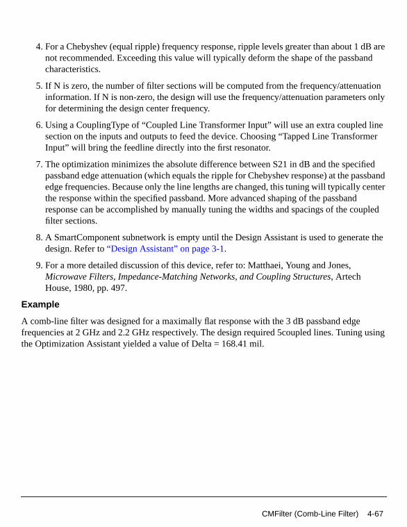
dB arend
tiononly
linermer
fiedssbandenter
upled
te the
using
4. For a Chebyshev (equal ripple) frequency response, ripple levels greater than about 1not recommended. Exceeding this value will typically deform the shape of the passbacharacteristics.
5. If N is zero, the number of filter sections will be computed from the frequency/attenuainformation. If N is non-zero, the design will use the frequency/attenuation parametersfor determining the design center frequency.
6. Using a CouplingType of “Coupled Line Transformer Input” will use an extra coupled section on the inputs and outputs to feed the device. Choosing “Tapped Line TransfoInput” will bring the feedline directly into the first resonator.
7. The optimization minimizes the absolute difference between S21 in dB and the specipassband edge attenuation (which equals the ripple for Chebyshev response) at the paedge frequencies. Because only the line lengths are changed, this tuning will typically cthe response within the specified passband. More advanced shaping of the passbandresponse can be accomplished by manually tuning the widths and spacings of the cofilter sections.
8. A SmartComponent subnetwork is empty until the Design Assistant is used to generadesign. Refer to“Design Assistant” on page 3-1.
9. For a more detailed discussion of this device, refer to: Matthaei, Young and Jones,Microwave Filters, Impedance-Matching Networks, and Coupling Structures, ArtechHouse, 1980, pp. 497.
Example
A comb-line filter was designed for a maximally flat response with the 3 dB passband edgefrequencies at 2 GHz and 2.2 GHz respectively. The design required 5coupled lines. Tuningthe Optimization Assistant yielded a value of Delta = 168.41 mil.
CMFilter (Comb-Line Filter) 4-67
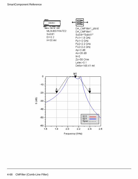
SmartComponent Reference
4-68 CMFilter (Comb-Line Filter)
ed)
ports.
dth.
delay
dB arend
HPFilter (Hairpin Filter)
Symbol
Parameters
Subst = microstrip substrate name
Fs1 = lower stopband edge frequency, in hertz
Fp1 = lower passband edge frequency, in hertz
Fp2 = upper passband edge frequency, in hertz
Fs2 = lower stopband edge frequency, in hertz
Ap = passband edge attenuation (or ripple for Chebyshev), in dB
As = stopband edge attenuation, in dB
N = number of filter sections (or 0 to compute N)
ResponseType = type of frequency response (maximally flat or Chebyshev)
Zo = desired input/output impedance, in ohms
Sphys = physical spacing between legs within hairpin resonator (set to zero if Selec specifi
Selec = spacing between legs within hairpin resonator in wavelengths (set to zero if Sphysspecified)
CouplingType = type of input/output coupling (coupled line or tapped line transformer)
Delta = length added to coupled sections for tuning performance
Notes
1. A hairpin filter provides a bandpass frequency response between the input and outputN coupled-line sections produce an N-1 order filter response. Additional numbers ofsections can be used to steepen the transition band roll off or widen the pass bandwi
2. Because of the heavy computational burden in determining the line parameters, a briefwill occur for the design.
3. For a Chebyshev (equal ripple) frequency response, ripple levels greater than about 1not recommended. Exceeding this value will typically deform the shape of the passbacharacteristics.
HPFilter (Hairpin Filter) 4-69

SmartComponent Reference
tiononly
mer
fiedssbandenter
upled
te the
and
. Thee of
4. If N is zero, the number of filter sections will be computed from the frequency/attenuainformation. If N is non-zero, the design will use the frequency/attenuation parametersfor determining the design center frequency.
5. Using a Coupled Line Transformer Input CouplingType will use and extra coupled linesection on the inputs and outputs to feed the device. Choosing Tapped Line TransforInput will bring the feedline directly into the first resonator.
6. The optimization minimizes the absolute difference between S21 in dB and the specipassband edge attenuation (which equals the ripple for Chebyshev response) at the paedge frequencies. Because only the line lengths are changed, this tuning will typically cthe response within the specified passband. More advanced shaping of the passbandresponse can be accomplished by manually tuning the widths and spacings of the cofilter sections.
7. A SmartComponent subnetwork is empty until the Design Assistant is used to generadesign. Refer to“Design Assistant” on page 3-1.
8. For a more detailed discussion of this device, refer to: Cristal and Frankel, “Hairpin-linehybrid hairpin-line/half-wave parallel-coupled-line filters,”IEEE Trans. Microwave Theoryand Techniques, vol MTT-20, pp. 719-728, 1972.
Example
A hairpin filter was designed for a maximally flat response with the 3 dB passband edgefrequencies at 2 GHz and 2.2 GHz respectively. Coupled line transformer inputs were useddesign required 4 coupled sections. Tuning using the Optimization Assistant yielded a valuDelta =−41.682 mil.
4-70 HPFilter (Hairpin Filter)
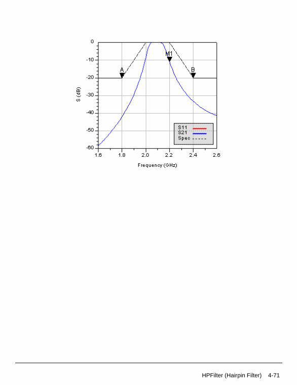
HPFilter (Hairpin Filter) 4-71

SmartComponent Reference
utputrs of
dth.
delay
dB arend
IDFilter (Interdigital Filter)
Symbol
Parameters
Subst = microstrip substrate name
Fs1 = lower stopband edge frequency, in hertz
Fp1 = lower passband edge frequency, in hertz
Fp2 = upper passband edge frequency, in hertz
Fs2 = lower stopband edge frequency, in hertz
Ap = passband edge attenuation (or ripple for Chebyshev), in dB
As = stopband edge attenuation, in dB
N = number of filter sections (or 0 to compute N)
ResponseType = type of frequency response (maximally flat or Chebyshev)
Zo = desired input/output impedance, in ohms
ya = normalized interior resonator admittance (0 < ya < 1)
CouplingType = type of input/output coupling (coupled line or tapped line transformer)
Delta = length added to coupled sections for tuning performance
Notes
1. An interdigital filter provides a bandpass frequency response between the input and oports. N coupled-line sections produce an N-1 order filter response. Additional numbesections can be used to steepen the transition band roll off or widen the pass bandwi
2. Because of the heavy computational burden in determining the line parameters, a briefwill occur for the design.
3. A two-layer substrate must be used for this topology.
4. For a Chebyshev (equal ripple) frequency response, ripple levels greater than about 1not recommended. Exceeding this value will typically deform the shape of the passbacharacteristics.
4-72 IDFilter (Interdigital Filter)
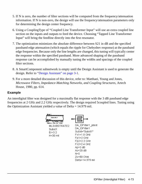
tiononly
linermer
fiedssbandenter
upled
te the
eusing
5. If N is zero, the number of filter sections will be computed from the frequency/attenuainformation. If N is non-zero, the design will use the frequency/attenuation parametersfor determining the design center frequency.
6. Using a CouplingType of “Coupled Line Transformer Input” will use an extra coupled section on the inputs and outputs to feed the device. Choosing “Tapped Line TransfoInput” will bring the feedline directly into the first resonator.
7. The optimization minimizes the absolute difference between S21 in dB and the specipassband edge attenuation (which equals the ripple for Chebyshev response) at the paedge frequencies. Because only the line lengths are changed, this tuning will typically cthe response within the specified passband. More advanced shaping of the passbandresponse can be accomplished by manually tuning the widths and spacings of the cofilter sections.
8. A SmartComponent subnetwork is empty until the Design Assistant is used to generadesign. Refer to“Design Assistant” on page 3-1.
9. For a more detailed discussion of this device, refer to: Matthaei, Young and Jones,Microwave Filters, Impedance-Matching Networks, and Coupling Structures, ArtechHouse, 1980, pp. 614.
Example
An interdigital filter was designed for a maximally flat response with the 3 dB passband edgfrequencies at 2 GHz and 2.2 GHz respectively. The design required 5coupled lines. Tuningthe Optimization Assistant yielded a value of Delta = 14.979 mil.
IDFilter (Interdigital Filter) 4-73
SmartComponent Reference
4-74 IDFilter (Interdigital Filter)
outputecified a
ces
SBFilter (Stub Bandpass Filter)
Symbol
Parameters
Subst = microstrip substrate name
Fs1 = lower stopband edge frequency, in hertz
Fp1 = lower passband edge frequency, in hertz
Fp2 = upper passband edge frequency, in hertz
Fs2 = lower stopband edge frequency, in hertz
Ap = passband edge attenuation (or ripple for Chebyshev), in dB
As = stopband edge attenuation, in dB
N = number of filter sections (or 0 to compute N)
ResponseType = type of frequency response (maximally flat or Chebyshev)
StubConfig = configuration of interior shunt stubs
Zo = desired input/output impedance, in ohms
D = impedance control parameter (0 < D < 1)
Delta = length added to stubs for tuning performance
Notes
1. A stub bandpass filter provides a bandpass frequency response between the input andports. The design uses shunt stubs connected by lengths of transmission line. If the sppassband response is too narrow, large differences in impedance values may result innon-realizable configuration.
2. This design is typically practical for fractional bandwidths of 0.4 to 0.7 or higher. If thebandwidth is too narrow, the design will generally require large differences in impedanbetween the stubs and the connecting lines, producing an unrealizable configuration.
SBFilter (Stub Bandpass Filter) 4-75
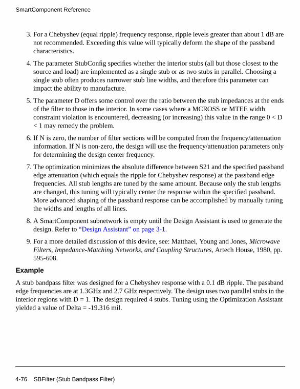
SmartComponent Reference
dB arend
o theing an
e ends
0 < D
tiononly
sbandedgengths
nd. tuning
te the
ssbands in theistant
3. For a Chebyshev (equal ripple) frequency response, ripple levels greater than about 1not recommended. Exceeding this value will typically deform the shape of the passbacharacteristics.
4. The parameter StubConfig specifies whether the interior stubs (all but those closest tsource and load) are implemented as a single stub or as two stubs in parallel. Choossingle stub often produces narrower stub line widths, and therefore this parameter caimpact the ability to manufacture.
5. The parameter D offers some control over the ratio between the stub impedances at thof the filter to those in the interior. In some cases where a MCROSS or MTEE widthconstraint violation is encountered, decreasing (or increasing) this value in the range < 1 may remedy the problem.
6. If N is zero, the number of filter sections will be computed from the frequency/attenuainformation. If N is non-zero, the design will use the frequency/attenuation parametersfor determining the design center frequency.
7. The optimization minimizes the absolute difference between S21 and the specified pasedge attenuation (which equals the ripple for Chebyshev response) at the passband frequencies. All stub lengths are tuned by the same amount. Because only the stub leare changed, this tuning will typically center the response within the specified passbaMore advanced shaping of the passband response can be accomplished by manuallythe widths and lengths of all lines.
8. A SmartComponent subnetwork is empty until the Design Assistant is used to generadesign. Refer to“Design Assistant” on page 3-1.
9. For a more detailed discussion of this device, see: Matthaei, Young and Jones,MicrowaveFilters, Impedance-Matching Networks, and Coupling Structures, Artech House, 1980, pp.595-608.
Example
A stub bandpass filter was designed for a Chebyshev response with a 0.1 dB ripple. The paedge frequencies are at 1.3GHz and 2.7 GHz respectively. The design uses two parallel stubinterior regions with D = 1. The design required 4 stubs. Tuning using the Optimization Assyielded a value of Delta = -19.316 mil.
4-76 SBFilter (Stub Bandpass Filter)
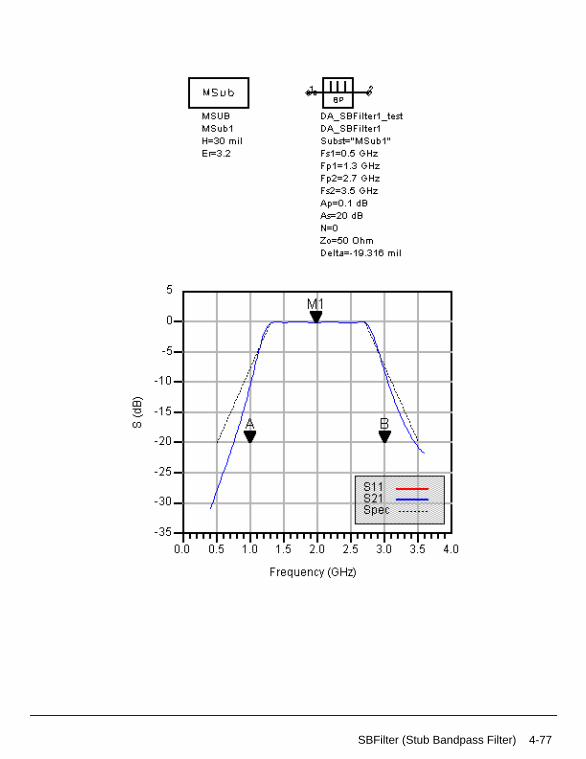
SBFilter (Stub Bandpass Filter) 4-77
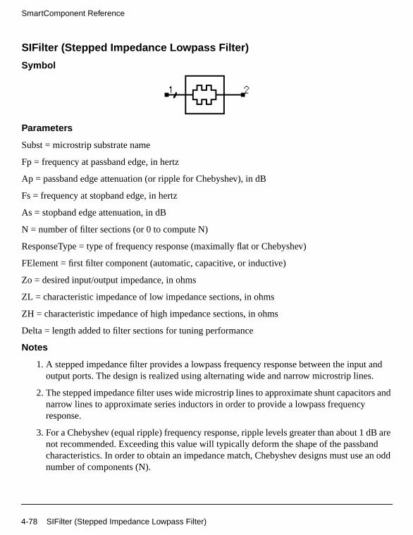
SmartComponent Reference
t and.
rs and
dB arendan odd
SIFilter (Stepped Impedance Lowpass Filter)
Symbol
Parameters
Subst = microstrip substrate name
Fp = frequency at passband edge, in hertz
Ap = passband edge attenuation (or ripple for Chebyshev), in dB
Fs = frequency at stopband edge, in hertz
As = stopband edge attenuation, in dB
N = number of filter sections (or 0 to compute N)
ResponseType = type of frequency response (maximally flat or Chebyshev)
FElement = first filter component (automatic, capacitive, or inductive)
Zo = desired input/output impedance, in ohms
ZL = characteristic impedance of low impedance sections, in ohms
ZH = characteristic impedance of high impedance sections, in ohms
Delta = length added to filter sections for tuning performance
Notes
1. A stepped impedance filter provides a lowpass frequency response between the inpuoutput ports. The design is realized using alternating wide and narrow microstrip lines
2. The stepped impedance filter uses wide microstrip lines to approximate shunt capacitonarrow lines to approximate series inductors in order to provide a lowpass frequencyresponse.
3. For a Chebyshev (equal ripple) frequency response, ripple levels greater than about 1not recommended. Exceeding this value will typically deform the shape of the passbacharacteristics. In order to obtain an impedance match, Chebyshev designs must usenumber of components (N).
4-78 SIFilter (Stepped Impedance Lowpass Filter)
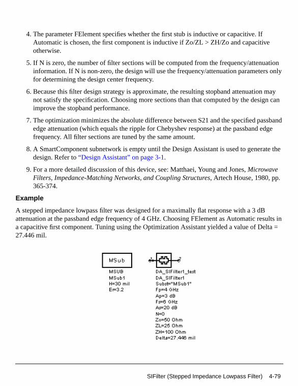
tiononly
mayn can
sbandedge
te the
sults inlta =
4. The parameter FElement specifies whether the first stub is inductive or capacitive. IfAutomatic is chosen, the first component is inductive if Zo/ZL > ZH/Zo and capacitiveotherwise.
5. If N is zero, the number of filter sections will be computed from the frequency/attenuainformation. If N is non-zero, the design will use the frequency/attenuation parametersfor determining the design center frequency.
6. Because this filter design strategy is approximate, the resulting stopband attenuationnot satisfy the specification. Choosing more sections than that computed by the desigimprove the stopband performance.
7. The optimization minimizes the absolute difference between S21 and the specified pasedge attenuation (which equals the ripple for Chebyshev response) at the passband frequency. All filter sections are tuned by the same amount.
8. A SmartComponent subnetwork is empty until the Design Assistant is used to generadesign. Refer to“Design Assistant” on page 3-1.
9. For a more detailed discussion of this device, see: Matthaei, Young and Jones,MicrowaveFilters, Impedance-Matching Networks, and Coupling Structures, Artech House, 1980, pp.365-374.
Example
A stepped impedance lowpass filter was designed for a maximally flat response with a 3 dBattenuation at the passband edge frequency of 4 GHz. Choosing FElement as Automatic rea capacitive first component. Tuning using the Optimization Assistant yielded a value of De27.446 mil.
SIFilter (Stepped Impedance Lowpass Filter) 4-79
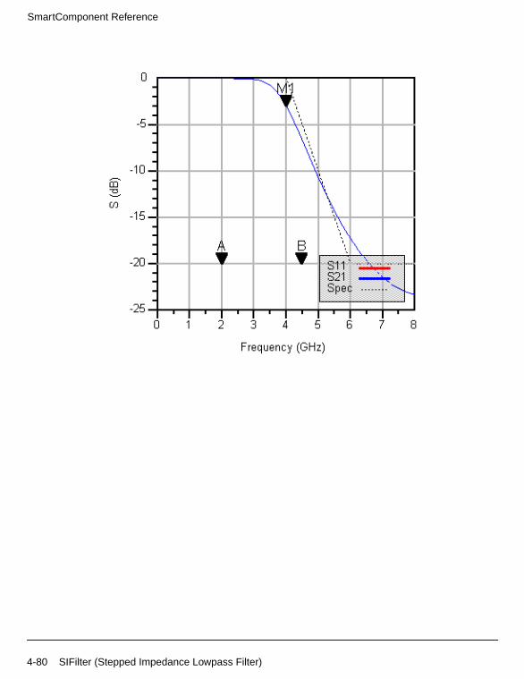
SmartComponent Reference
4-80 SIFilter (Stepped Impedance Lowpass Filter)
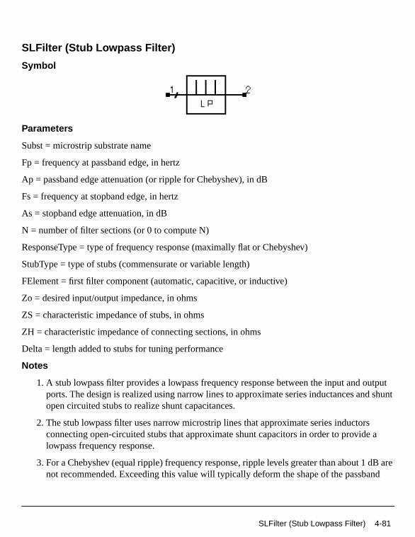
utputshunt
a
dB arend
SLFilter (Stub Lowpass Filter)
Symbol
Parameters
Subst = microstrip substrate name
Fp = frequency at passband edge, in hertz
Ap = passband edge attenuation (or ripple for Chebyshev), in dB
Fs = frequency at stopband edge, in hertz
As = stopband edge attenuation, in dB
N = number of filter sections (or 0 to compute N)
ResponseType = type of frequency response (maximally flat or Chebyshev)
StubType = type of stubs (commensurate or variable length)
FElement = first filter component (automatic, capacitive, or inductive)
Zo = desired input/output impedance, in ohms
ZS = characteristic impedance of stubs, in ohms
ZH = characteristic impedance of connecting sections, in ohms
Delta = length added to stubs for tuning performance
Notes
1. A stub lowpass filter provides a lowpass frequency response between the input and oports. The design is realized using narrow lines to approximate series inductances andopen circuited stubs to realize shunt capacitances.
2. The stub lowpass filter uses narrow microstrip lines that approximate series inductorsconnecting open-circuited stubs that approximate shunt capacitors in order to providelowpass frequency response.
3. For a Chebyshev (equal ripple) frequency response, ripple levels greater than about 1not recommended. Exceeding this value will typically deform the shape of the passba
SLFilter (Stub Lowpass Filter) 4-81

SmartComponent Reference
an odd
nd the mayre
er
tiononly
osing
sbandedge
te the
theesultedDelta
characteristics. In order to obtain an impedance match, Chebyshev designs must usenumber of components (N).
4. If the parameter StubType is set as Commensurate, all stubs will have equal lengths, astub line width is computed. The value of ZS is then ignored, and the resulting designbe difficult to realize. If StubType is set as Variable Length Stub, the stub line widths adetermined from ZS and the stub lengths are computed from the specifications.
5. The parameter FElement specifies whether the first stub is inductive or capacitive. IfAutomatic is chosen, the first component is set to be capacitive since this tends to offimprovements in manufacturing.
6. If N is zero, the number of filter sections will be computed from the frequency/attenuainformation. If N is non-zero, the design will use the frequency/attenuation parametersfor determining the design center frequency. Because this filter design strategy isapproximate, the resulting stopband attenuation may not satisfy the specification. Chomore sections than that computed by the Design Assistant can improve the stopbandperformance.
7. The optimization minimizes the absolute difference between S21 and the specified pasedge attenuation (which equals the ripple for Chebyshev response) at the passband frequency by changing the stub lengths. All stubs are tuned by the same amount.
8. A SmartComponent subnetwork is empty until the Design Assistant is used to generadesign. Refer to“Design Assistant” on page 3-1.
9. For a more detailed discussion of this device, refer to: Matthaei, Young and Jones,Microwave Filters, Impedance-Matching Networks, and Coupling Structures, ArtechHouse, 1980, pp. 375.
Example
A stub lowpass filter was designed for a maximally flat response with a 3 dB attenuation at passband edge frequency of 1 GHz. A variable length StubType and automatic FElement rin 13 components for the design. Tuning using the Optimization Assistant yielded a value of= 164.04 mil.
4-82 SLFilter (Stub Lowpass Filter)
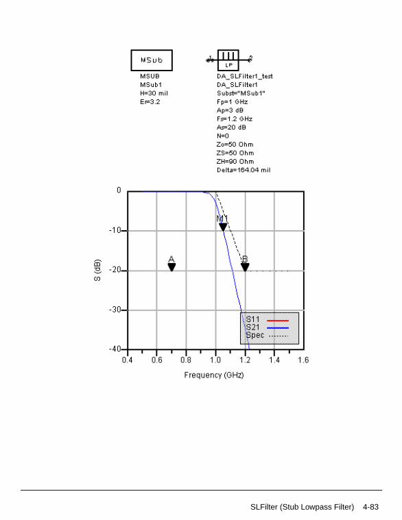
SLFilter (Stub Lowpass Filter) 4-83

SmartComponent Reference
een the
idenetal
delay
dB arend
SRFilter (Stepped Impedance Resonator Filter)
Symbol
Parameters
Subst = microstrip substrate name
Fs1 = lower stopband edge frequency, in hertz
Fp1 = lower passband edge frequency, in hertz
Fp2 = upper passband edge frequency, in hertz
Fs2 = lower stopband edge frequency, in hertz
Ap = passband edge attenuation (or ripple for Chebyshev), in dB
As = stopband edge attenuation, in dB
N = number of filter sections (or 0 to compute N)
ResponseType = type of frequency response (maximally flat or Chebyshev)
Zo = desired input/output impedance, in ohms
Fsp = center frequency of first spurious passband
Delta = length added to filter sections for tuning performance
Notes
1. A stepped impedance resonator filter provides a bandpass frequency response betwinput and output ports. N coupled-line sections produce an N−1 order filter response.Additional numbers of sections can be used to steepen the transition band roll off or wthe pass bandwidth. The use on non-uniform impedance for each resonator moves thsecond pass band center frequency away from the second harmonic of the fundamenfrequency.
2. Because of the heavy computational burden in determining the line parameters, a briefwill occur for the design.
3. For a Chebyshev (equal ripple) frequency response, ripple levels greater than about 1not recommended. Exceeding this value will typically deform the shape of the passbacharacteristics.
4-84 SRFilter (Stepped Impedance Resonator Filter)
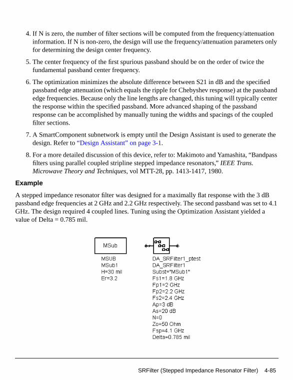
tiononly
he
fiedssbandenter
upled
te the
pass
dBet to 4.1
a
4. If N is zero, the number of filter sections will be computed from the frequency/attenuainformation. If N is non-zero, the design will use the frequency/attenuation parametersfor determining the design center frequency.
5. The center frequency of the first spurious passband should be on the order of twice tfundamental passband center frequency.
6. The optimization minimizes the absolute difference between S21 in dB and the specipassband edge attenuation (which equals the ripple for Chebyshev response) at the paedge frequencies. Because only the line lengths are changed, this tuning will typically cthe response within the specified passband. More advanced shaping of the passbandresponse can be accomplished by manually tuning the widths and spacings of the cofilter sections.
7. A SmartComponent subnetwork is empty until the Design Assistant is used to generadesign. Refer to“Design Assistant” on page 3-1.
8. For a more detailed discussion of this device, refer to: Makimoto and Yamashita, “Bandfilters using parallel coupled stripline stepped impedance resonators,”IEEE Trans.Microwave Theory and Techniques, vol MTT-28, pp. 1413-1417, 1980.
Example
A stepped impedance resonator filter was designed for a maximally flat response with the 3passband edge frequencies at 2 GHz and 2.2 GHz respectively. The second passband was sGHz. The design required 4 coupled lines. Tuning using the Optimization Assistant yieldedvalue of Delta = 0.785 mil.
SRFilter (Stepped Impedance Resonator Filter) 4-85
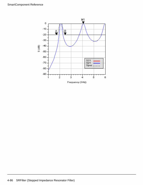
SmartComponent Reference
4-86 SRFilter (Stepped Impedance Resonator Filter)

ut andnd
delay
dB arend
tiononly
sbandedge
ZZFilter (Zig-Zag Coupled-Line Filter)
Symbol
Parameters
Subst = microstrip substrate name
Fs1 = lower stopband edge frequency, in hertz
Fp1 = lower passband edge frequency, in hertz
Fp2 = upper passband edge frequency, in hertz
Ap = passband edge attenuation (or ripple for Chebyshev), in dB
As = stopband edge attenuation, in dB
N = number of filter sections (or 0 to compute N)
ResponseType = type of frequency response (maximally flat or Chebyshev)
Zo = desired input/output impedance, in ohms
Delta = length added to coupled sections for tuning performance
Notes
1. A zig-zag coupled-line filter provides a bandpass frequency response between the inpoutput ports. The design uses a coupled-line filter topology but includes 90 degree bebetween each coupled section so that the layout is more compact.
2. Because of the heavy computational burden in determining the line parameters, a briefwill occur for the design.
3. For a Chebyshev (equal ripple) frequency response, ripple levels greater than about 1not recommended. Exceeding this value will typically deform the shape of the passbacharacteristics.
4. If N is zero, the number of filter sections will be computed from the frequency/attenuainformation. If N is non-zero, the design will use the frequency/attenuation parametersfor determining the design center frequency.
5. The optimization minimizes the absolute difference between S21 and the specified pasedge attenuation (which equals the ripple for Chebyshev response) at the passband
ZZFilter (Zig-Zag Coupled-Line Filter) 4-87

SmartComponent Reference
er theponse
r
te the
andctions.
frequencies. Because only the line lengths are changed, this tuning will typically centresponse within the specified passband. More advanced shaping of the passband rescan be accomplished by manually tuning the widths and spacings of the coupled filtesections.
6. A SmartComponent subnetwork is empty until the Design Assistant is used to generadesign. Refer to“Design Assistant” on page 3-1.
7. For a more detailed discussion of this device, see: D. M. Pozar,Microwave Engineering,2nd Edition, John Wiley & Sons: New York, 1998, pp. 477-485.
Example
A zig-zag coupled-line filter was designed for a maximally flat response with the 3 dB passbedge frequencies at 2 GHz and 2.4 GHz respectively. The design required 4 coupled-line seTuning using the Optimization Assistant yielded a value of Delta = -6.233 mil.
4-88 ZZFilter (Zig-Zag Coupled-Line Filter)
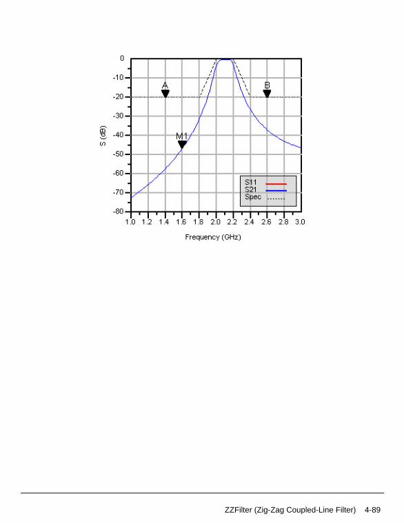
ZZFilter (Zig-Zag Coupled-Line Filter) 4-89

SmartComponent Reference
sired
some
ostrip
Passive Circuit DG - Matching
DSMatch (Double-Stub Match)
Symbol
Parameters
Subst = microstrip substrate name
F = center frequency, in hertz
Zin = desired complex input impedance, in ohms
Zload = complex load impedance to match, in ohms
Zstub1 = characteristic impedance of stub line 1 (nearest input), in ohms
Zstub2 = characteristic impedance of stub line 2 (nearest output), in ohms
Zline = characteristic impedance of line between stubs, in ohms
Zfeed1 = characteristic impedance of line connected to port 1, in ohms
Zfeed2 = characteristic impedance of line connected to port 2, in ohms
Stub1Type = stub 1 type (open or short circuit)
Stub2Type = stub 2 type (open or short circuit)
Delta = length added to stubs for tuning performance
Notes
1. A double-stub matching network matches a complex load impedance (Zload) to a decomplex input impedance (Zin) using two shunt stubs and a connecting line.
2. An impedance match can be realized using any combination of stub types, although combinations may be more realizable.
3. Zfeed1 and Zfeed2 are used simply to ensure that the input and output legs of the micrtee components are of the proper width.
4-90 DSMatch (Double-Stub Match)

such
ilar
b 1 islize a
n
e the
te the
s to a
4. The length of the line between the stubs is nominally chosen to be an eighth of a linewavelength. However, if this will not realize the match, the length of line is computed that the rotated circle on the Smith chart encloses the load admittance.
5. MTEE component width constraint violations will be avoided generally by choosing simcharacteristic impedances for the line, stub, and feed.
6. Since two solutions are possible, the solution that results in the smallest length of stuchosen. For example, if stub 1 is open circuited, the solution for which stub 1 must reacapacitive reactance is chosen.
7. The input port termination is set to the conjugate of Zin so that the ideal input reflectiocoefficient will be zero. The output port termination is set to Zload.
8. The optimization minimizes the value of S11 (referenced to the conjugate of Zin) at thdesign center frequency by changing the length of the stubs. Both stubs are tuned bysame length.
9. A SmartComponent subnetwork is empty until the Design Assistant is used to generadesign. Refer to“Design Assistant” on page 3-1.
10. For a more detailed discussion of this device, see: D. M. Pozar,Microwave Engineering,2nd Edition, John Wiley & Sons: New York, 1998, pp. 266-271.
Example
A double-stub matching network was designed to match a load impedance of 100 - j30 ohm50 ohm line at a center frequency of 5 GHz with open circuited stubs. Tuning using theOptimization Assistant yielded a value of Delta =-31.633 mil.
DSMatch (Double-Stub Match) 4-91
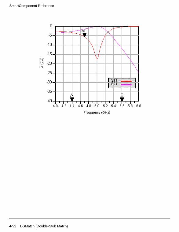
SmartComponent Reference
4-92 DSMatch (Double-Stub Match)
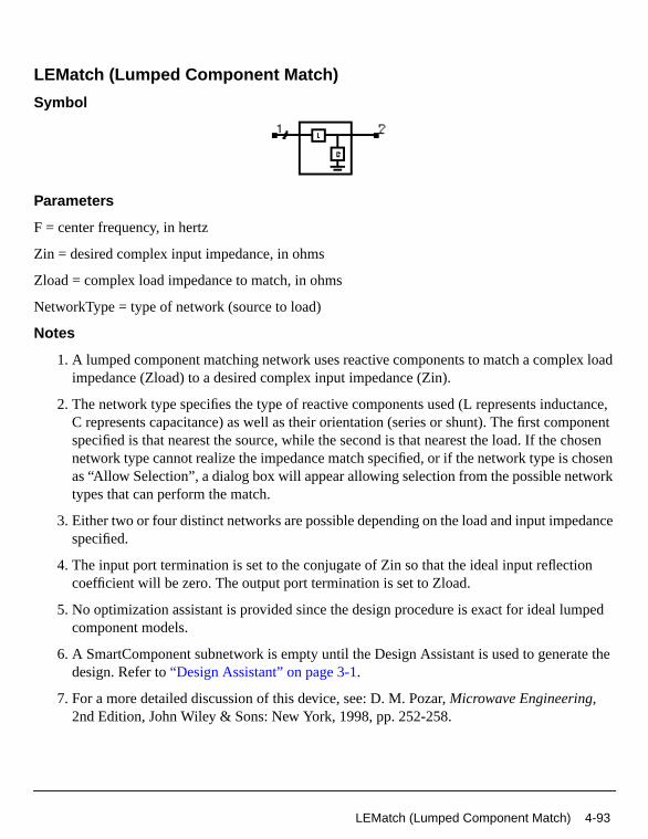
x load
tance,ponenthosenosen
ork
ance
n
ped
te the
LEMatch (Lumped Component Match)
Symbol
Parameters
F = center frequency, in hertz
Zin = desired complex input impedance, in ohms
Zload = complex load impedance to match, in ohms
NetworkType = type of network (source to load)
Notes
1. A lumped component matching network uses reactive components to match a compleimpedance (Zload) to a desired complex input impedance (Zin).
2. The network type specifies the type of reactive components used (L represents inducC represents capacitance) as well as their orientation (series or shunt). The first comspecified is that nearest the source, while the second is that nearest the load. If the cnetwork type cannot realize the impedance match specified, or if the network type is chas “Allow Selection”, a dialog box will appear allowing selection from the possible netwtypes that can perform the match.
3. Either two or four distinct networks are possible depending on the load and input impedspecified.
4. The input port termination is set to the conjugate of Zin so that the ideal input reflectiocoefficient will be zero. The output port termination is set to Zload.
5. No optimization assistant is provided since the design procedure is exact for ideal lumcomponent models.
6. A SmartComponent subnetwork is empty until the Design Assistant is used to generadesign. Refer to“Design Assistant” on page 3-1.
7. For a more detailed discussion of this device, see: D. M. Pozar,Microwave Engineering,2nd Edition, John Wiley & Sons: New York, 1998, pp. 252-258.
LEMatch (Lumped Component Match) 4-93
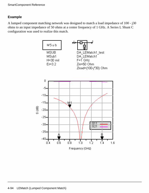
SmartComponent Reference
j30C
Example
A lumped component matching network was designed to match a load impedance of 100 -ohms to an input impedance of 50 ohms at a center frequency of 1 GHz. A Series L Shunt configuration was used to realize this match.
4-94 LEMatch (Lumped Component Match)

d realcy
hewidth
t eache in
.
)
QWMatch (Quarter-Wave Match)
Symbol
Parameters
Subst = microstrip substrate name
F = center frequency, in hertz
DeltaF = total frequency bandwidth, in hertz
Zo = desired input impedance, in ohms
Rload = load impedance to match, in ohms
ResponseType = type of frequency response
N = number of quarter-wave sections (set N=0 to compute N)
Rmax = maximum voltage reflection coefficient
Delta = length added to transformer sections for tuning performance
Notes
1. A quarter-wave matching network matches a real load impedance (Rload) to a desireinput impedance (Zo) using multiple quarter wavelength sections. A specified frequenresponse can be realized by proper design of the individual sections.
2. DeltaF is defined as the total bandwidth centered at the design center frequency.
3. If the number of sections N is set to zero, the Design Assistant chooses N such that treflection coefficient is less that Rmax over the bandwidth DeltaF. The resulting bandmay be broader than that specified. Otherwise, Rmax and DeltaF are ignored.
4. The ResponseType specifies the distribution of the partial reflection coefficients seen asection interface - Uniform, Binomial, and Chebyshev distributions are available. Thesturn specify the shape of the reflection coefficient versus frequency.
5. A single-section quarter-wave matching transformer can be designed by setting N = 1
6. Since the reflection coefficient may not be at its minimum value at the design centerfrequency, the optimization centers the variation of S11 (referenced to the value of Zo
QWMatch (Quarter-Wave Match) 4-95
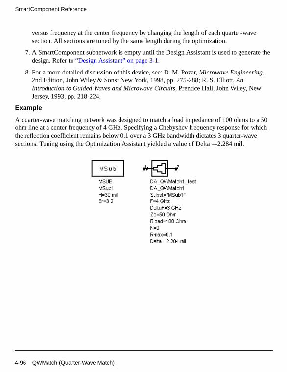
SmartComponent Reference
e
te the
a 50hich
versus frequency at the center frequency by changing the length of each quarter-wavsection. All sections are tuned by the same length during the optimization.
7. A SmartComponent subnetwork is empty until the Design Assistant is used to generadesign. Refer to“Design Assistant” on page 3-1.
8. For a more detailed discussion of this device, see: D. M. Pozar,Microwave Engineering,2nd Edition, John Wiley & Sons: New York, 1998, pp. 275-288; R. S. Elliott,AnIntroduction to Guided Waves and Microwave Circuits, Prentice Hall, John Wiley, NewJersey, 1993, pp. 218-224.
Example
A quarter-wave matching network was designed to match a load impedance of 100 ohms toohm line at a center frequency of 4 GHz. Specifying a Chebyshev frequency response for wthe reflection coefficient remains below 0.1 over a 3 GHz bandwidth dictates 3 quarter-wavesections. Tuning using the Optimization Assistant yielded a value of Delta =-2.284 mil.
4-96 QWMatch (Quarter-Wave Match)
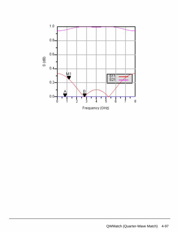
QWMatch (Quarter-Wave Match) 4-97

SmartComponent Reference
t and
for the
.
ut
te the
RAtten (Resistive Attenuator)
Symbol
Parameters
Loss = attenuation, in dB
Rin = input resistance, in ohms
Rout = output resistance, in ohms
DesignType = length added to ring branches for tuning
Notes
1. A resistive attenuator achieves a specified attenuation while maintaining desired inpuoutput impedance levels.
2. The design specifies the resistance values to achieve the specified level of attenuationinput and output resistances.
3. The input resistance Rin must be greater than or equal to the output resistance Rout
4. There is a minimum attenuation that can be achieved for the specified input and outpresistances. This attenuation is given by:
5. A SmartComponent subnetwork is empty until the Design Assistant is used to generadesign. Refer to“Design Assistant” on page 3-1.
Example
A 3-dB tee attenuator was designed for a 50 ohm input and output resistance.
MinimumLoss 20 RinRout------------ Rin
Rout------------ 1–+
log=
4-98 RAtten (Resistive Attenuator)
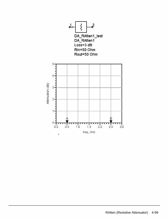
RAtten (Resistive Attenuator) 4-99
SmartComponent Reference
ired
oicestwork
g bothoosing
g onhe stub
SSMatch (Single-Stub Match)
Symbol
Parameters
Subst = microstrip substrate name
F = center frequency, in hertz
Zin = desired complex input impedance, in ohms
Zload = complex load impedance to match, in ohms
Zstub = characteristic impedance of stub line, in ohms
Zline = characteristic impedance of line, in ohms
Zfeed = characteristic impedance of line connected to port 1 or 2, in ohms
StubType = stub type (open or short circuit)
NetType = network type (source to load)
Delta = length added to stub for tuning performance
Notes
1. A single-stub matching network matches a complex load impedance (Zload) to a descomplex input impedance (Zin) using a single shunt stub and length of line.
2. The parameter NetType can be Automatic, stub-line, or line-stub, with the latter two chrepresenting configurations that have a stub followed by a line or vice-versa as the neis observed from source to load. Many impedance combinations can be realized usinpossible types, although some can only be realized using one of the two choices. ChAutomatic will ensure a realizable choice is given.
3. An impedance match can be realized using either stub type.
4. Zline represents the impedance of the line either next to the source or load (dependinthe value of NetType). Zfeed represents the desired impedance on the other side of tfrom the line and is used to ensure that the corresponding leg of the microstrip teecomponent is of the proper width.
4-100 SSMatch (Single-Stub Match)

ilar
n
e
te the
s to action
t
5. MTEE component width constraint violations will be avoided generally by choosing simcharacteristic impedances for the line, stub, and feed.
6. The input port termination is set to the conjugate of Zin so that the ideal input reflectiocoefficient will be zero. The output port termination is set to Zload.
7. The optimization minimizes the value of S11 (referenced to the conjugate of Zin) at thdesign center frequency by changing the length of the stub.
8. A SmartComponent subnetwork is empty until the Design Assistant is used to generadesign. Refer to“Design Assistant” on page 3-1.
9. For a more detailed discussion of this device, see: D. M. Pozar,Microwave Engineering,2nd Edition, John Wiley & Sons: New York, 1998, pp. 258-266.
Example
A single-stub matching network was designed to match a load impedance of 100 - j25 ohm50 ohm line at a center frequency of 2GHz. Choosing an open-circuit stub with automatic seleof the NetType resulted in a stub-line configuration. Tuning using the Optimization Assistanyielded a value of Delta =-5.078 mil.
SSMatch (Single-Stub Match) 4-101
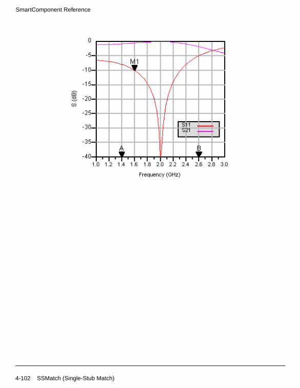
SmartComponent Reference
4-102 SSMatch (Single-Stub Match)
realalize
linear
.
line
ts.
TLMatch (Tapered-Line Match)
Symbol
Parameters
Subst = microstrip substrate name
F = design frequency, in hertz
Zo = desired input impedance, in ohms
Rload = load impedance to match, in ohms
ResponseType = type of frequency response (exponential, triangular, Klopfenstein)
L = length of tapered line in wavelengths at frequency F (set L=0 to compute L)
Rmax = maximum voltage reflection coefficient
NSection = number of linear taper sections per wavelength
Notes
1. A tapered-line matching network matches a real load impedance (Rload) to a desiredinput impedance (Zo) using a continuously varying line characteristic impedance to rea specified frequency response. The reflection coefficient remains below the specifiedmaximum value for all frequencies above the design frequency.
2. The continuous impedance taper of this circuit is approximated using a sequence of tapers. Increasing the number of sections per wavelength (NSection) will improve theapproximation to the defined taper.
3. If the length of the line L is set to zero, the Design Assistant chooses L such that thereflection coefficient is less than Rmax for all frequencies above the design frequencyOtherwise, Rmax is ignored.
4. The ResponseType specifies the distribution of the impedance along the length of theand therefore determines the frequency response of the match.
5. No Optimization Assistant is provided since the design process is exact to within theapproximation of the continuous impedance taper using multiple linear taper segmenIncreasing the value of NSection will improve the computed response.
TLMatch (Tapered-Line Match) 4-103
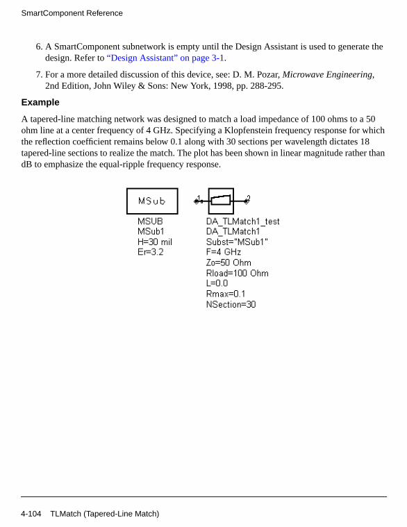
SmartComponent Reference
te the
a 50hich
18er than
6. A SmartComponent subnetwork is empty until the Design Assistant is used to generadesign. Refer to“Design Assistant” on page 3-1.
7. For a more detailed discussion of this device, see: D. M. Pozar,Microwave Engineering,2nd Edition, John Wiley & Sons: New York, 1998, pp. 288-295.
Example
A tapered-line matching network was designed to match a load impedance of 100 ohms toohm line at a center frequency of 4 GHz. Specifying a Klopfenstein frequency response for wthe reflection coefficient remains below 0.1 along with 30 sections per wavelength dictates tapered-line sections to realize the match. The plot has been shown in linear magnitude rathdB to emphasize the equal-ripple frequency response.
4-104 TLMatch (Tapered-Line Match)
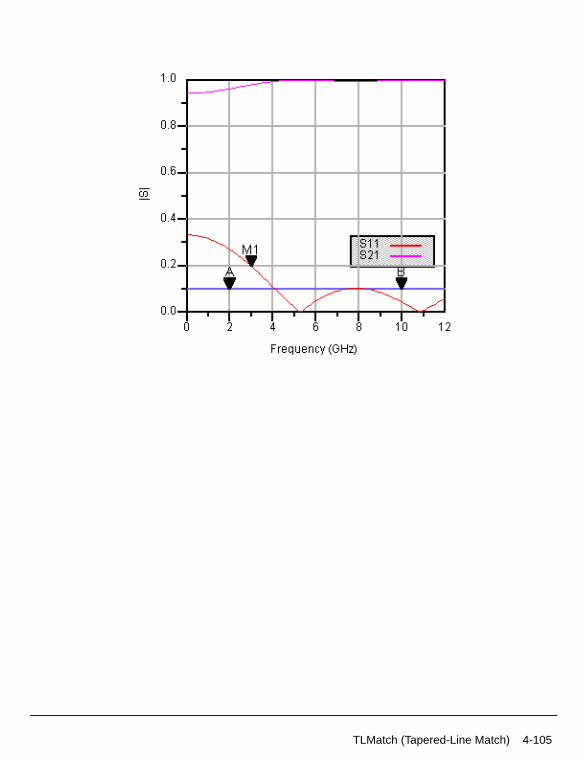
TLMatch (Tapered-Line Match) 4-105

SmartComponent Reference
4-106 Passive Circuit DG - Matching
Index
Aartwork, layout, 3-10BBLCoupler, 4-49
CCLCoupler, 4-52CLFilter, 4-63CMFilter, 4-66Control Window, using, 1-9coupler components, 4-2
DDesign Assistant, using, 3-1DSMatch, 4-90
Eexamples, 1-11
Ffilter components, 4-2
HHPFilter, 4-69
IIDFilter, 4-72
Llayouts, updating, 3-10LCoupler, 4-54LEMatch, 4-93line components, 4-1
Mmatching components, 4-3MBend, 4-4MBStub, 4-5MCFil, 4-7MCLine, 4-8MCorn, 4-9MCross, 4-10MCurve, 4-11MGap, 4-12MICapP, 4-22
MICapPG, 4-25MICapS, 4-28MICapSG, 4-31MLine, 4-13MMndr, 4-14MREInd, 4-34MRInd, 4-37MRStub, 4-16MSInd, 4-40MStep, 4-18MStub, 4-19MTaper, 4-20MTee, 4-21MTFC, 4-42
Nnavigation, 1-6
Ooverview, 1-1
QQWMatch, 4-95
RRAtten, 4-98RLC components, 4-2RRCoupler, 4-56
SSBFilter, 4-75SIFilter, 4-78SLFilter, 4-81SmartComponent, 4-1SRFilter, 4-84SSMatch, 4-100
TTCoupler, 4-58TFC, 4-45TFR, 4-47TLMatch, 4-103
WWDCoupler, 4-60
Index-1

ZZZFilter, 4-87
Index-2