Embed Size (px)
Citation preview
Improve Design Performance & Yield
© Copyright by MunEDA GmbH - All rights reserved - www.muneda.com
Parameterize behavioral models using
WiCkeD Modeling
Demonstrator:
Charge Pump Phase Locked Loop (CP-PLL)
Dr. Volker Glöckel

Improve Design Performance & Yield
© Copyright by MunEDA GmbH - All rights reserved - www.muneda.com
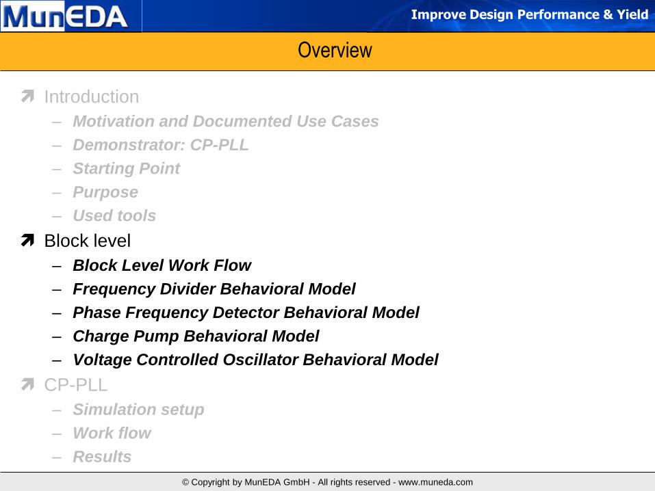
Overview
Introduction
– Motivation and Documented Use Cases
– Demonstrator: CP-PLL
– Starting Point
– Purpose of applying WiCkeD Modeling
– Used tools
Block level
– Block Level Work Flow
– Frequency Divider Behavioral Model
– Phase Frequency Detector Behavioral Model
– Charge Pump Behavioral Model
– Voltage Controlled Oscillator Behavioral Model
CP-PLL
– Simulation setup
– Work flow
– Results
Improve Design Performance & Yield
© Copyright by MunEDA GmbH - All rights reserved - www.muneda.com
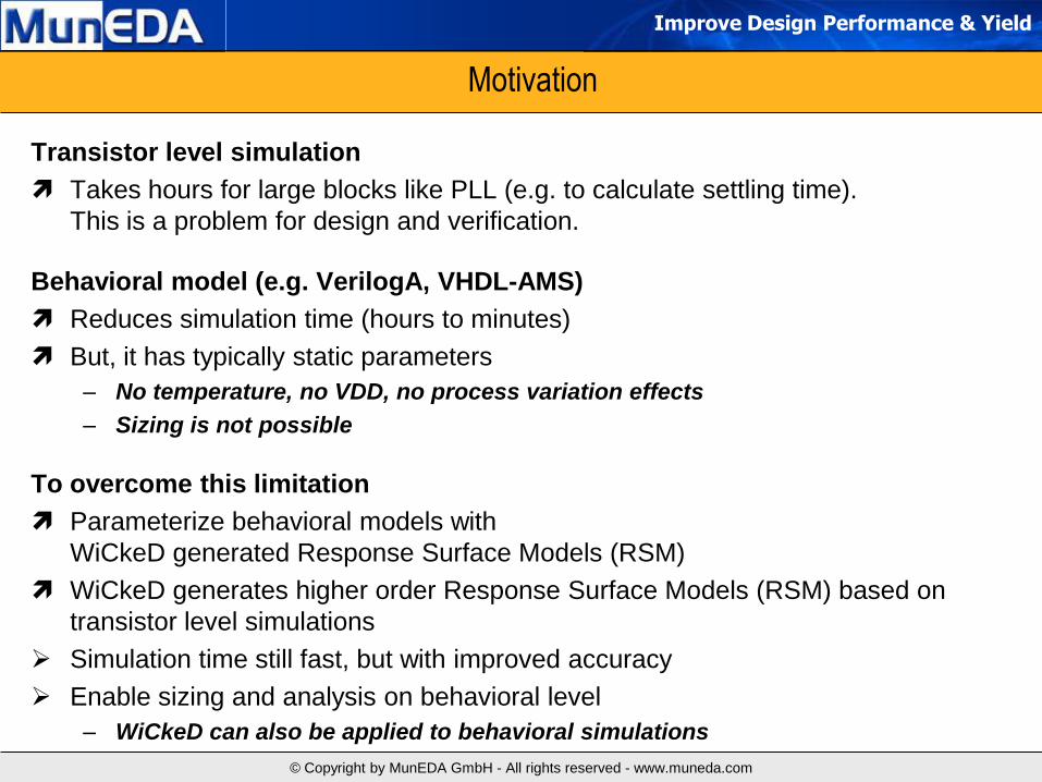
Motivation
Transistor level simulation
Takes hours for large blocks like PLL (e.g. to calculate settling time).
This is a problem for design and verification.
Behavioral model (e.g. VerilogA, VHDL-AMS)
Reduces simulation time (hours to minutes)
But, it has typically static parameters
– No temperature, no VDD, no process variation effects
– Sizing is not possible
To overcome this limitation
Parameterize behavioral models with
WiCkeD generated Response Surface Models (RSM)
WiCkeD generates higher order Response Surface Models (RSM) based on
transistor level simulations
Simulation time still fast, but with improved accuracy
Enable sizing and analysis on behavioral level
– WiCkeD can also be applied to behavioral simulations
Improve Design Performance & Yield
© Copyright by MunEDA GmbH - All rights reserved - www.muneda.com
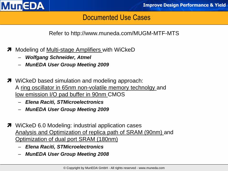
Documented Use Cases
Refer to http://www.muneda.com/MUGM-MTF-MTS
Modeling of Multi-stage Amplifiers with WiCkeD
– Wolfgang Schneider, Atmel
– MunEDA User Group Meeting 2009
WiCkeD based simulation and modeling approach:
A ring oscillator in 65nm non-volatile memory technolgy and
low emission I/O pad buffer in 90nm CMOS
– Elena Raciti, STMicroelectronics
– MunEDA User Group Meeting 2009
WiCkeD 6.0 Modeling: industrial application cases
Analysis and Optimization of replica path of SRAM (90nm) and
Optimization of dual port SRAM (180nm)
– Elena Raciti, STMicroelectronics
– MunEDA User Group Meeting 2008
Improve Design Performance & Yield
© Copyright by MunEDA GmbH - All rights reserved - www.muneda.com
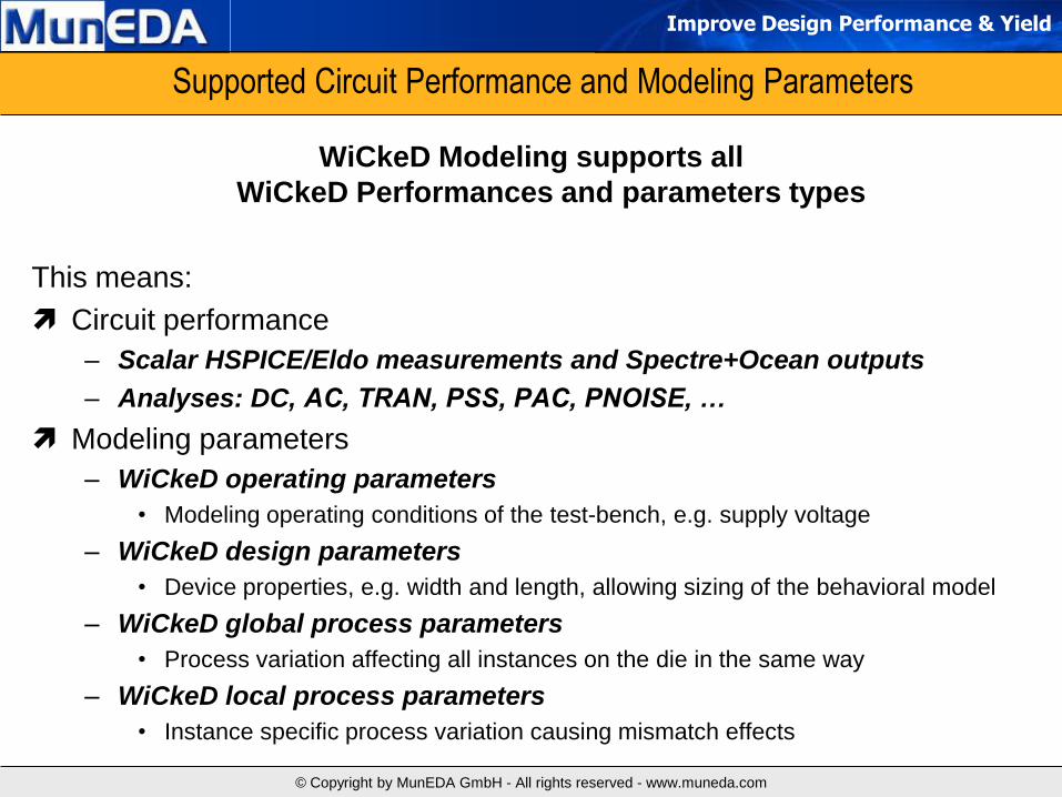
Supported Circuit Performance and Modeling Parameters
WiCkeD Modeling supports all
WiCkeD Performances and parameters types
This means:
Circuit performance
– Scalar HSPICE/Eldo measurements and Spectre+Ocean outputs
– Analyses: DC, AC, TRAN, PSS, PAC, PNOISE, …
Modeling parameters
– WiCkeD operating parameters
• Modeling operating conditions of the test-bench, e.g. supply voltage
– WiCkeD design parameters
• Device properties, e.g. width and length, allowing sizing of the behavioral model
– WiCkeD global process parameters
• Process variation affecting all instances on the die in the same way
– WiCkeD local process parameters
• Instance specific process variation causing mismatch effects
Improve Design Performance & Yield
© Copyright by MunEDA GmbH - All rights reserved - www.muneda.com
Supported Circuit Performance and Modeling Parameters
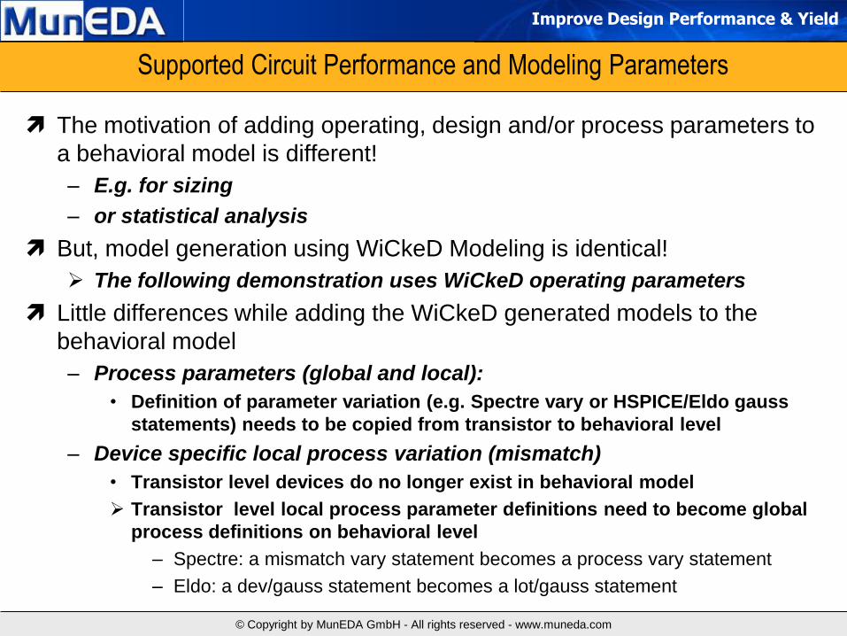
The motivation of adding operating, design and/or process parameters to
a behavioral model is different!
– E.g. for sizing
– or statistical analysis
But, model generation using WiCkeD Modeling is identical!
The following demonstration uses WiCkeD operating parameters
Little differences while adding the WiCkeD generated models to the
behavioral model
– Process parameters (global and local):
• Definition of parameter variation (e.g. Spectre vary or HSPICE/Eldo gauss
statements) needs to be copied from transistor to behavioral level
– Device specific local process variation (mismatch)
• Transistor level devices do no longer exist in behavioral model
Transistor level local process parameter definitions need to become global
process definitions on behavioral level
– Spectre: a mismatch vary statement becomes a process vary statement
– Eldo: a dev/gauss statement becomes a lot/gauss statement

Improve Design Performance & Yield
© Copyright by MunEDA GmbH - All rights reserved - www.muneda.com
Demonstrator: Charge Pump Phase Locked Loop (CP-PLL)
* LF: ideal C and R elements so far - no modeling necessary
Phase
Frequency
Detector
Charge
Pump
Loop
Filter
Voltage
Controlled
Oscillator
Frequency
Divider
:2
250MHz up (active low)
down
500MHz
ctrl
Descriptions PFD CP LF VCO FD
Transistor level
VerilogA + WiCkeD RSM *
Improve Design Performance & Yield
© Copyright by MunEDA GmbH - All rights reserved - www.muneda.com
Starting point
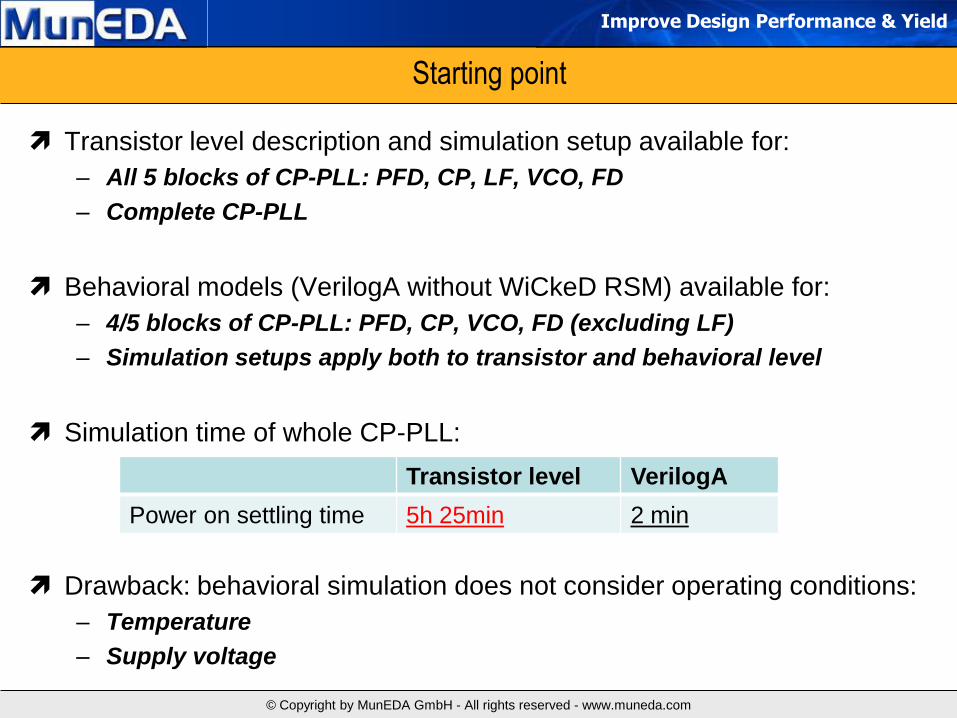
Transistor level description and simulation setup available for:
– All 5 blocks of CP-PLL: PFD, CP, LF, VCO, FD
– Complete CP-PLL
Behavioral models (VerilogA without WiCkeD RSM) available for:
– 4/5 blocks of CP-PLL: PFD, CP, VCO, FD (excluding LF)
– Simulation setups apply both to transistor and behavioral level
Simulation time of whole CP-PLL:
Drawback: behavioral simulation does not consider operating conditions:
– Temperature
– Supply voltage
Transistor level VerilogA
Power on settling time 5h 25min 2 min
Improve Design Performance & Yield
© Copyright by MunEDA GmbH - All rights reserved - www.muneda.com
Purpose
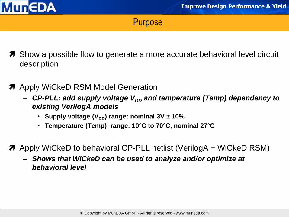
Show a possible flow to generate a more accurate behavioral level circuit
description
Apply WiCkeD RSM Model Generation
– CP-PLL: add supply voltage VDD and temperature (Temp) dependency to
existing VerilogA models
• Supply voltage (VDD) range: nominal 3V ± 10%
• Temperature (Temp) range: 10°C to 70°C, nominal 27°C
Apply WiCkeD to behavioral CP-PLL netlist (VerilogA + WiCkeD RSM)
– Shows that WiCkeD can be used to analyze and/or optimize at
behavioral level
Improve Design Performance & Yield
© Copyright by MunEDA GmbH - All rights reserved - www.muneda.com
Used Tools
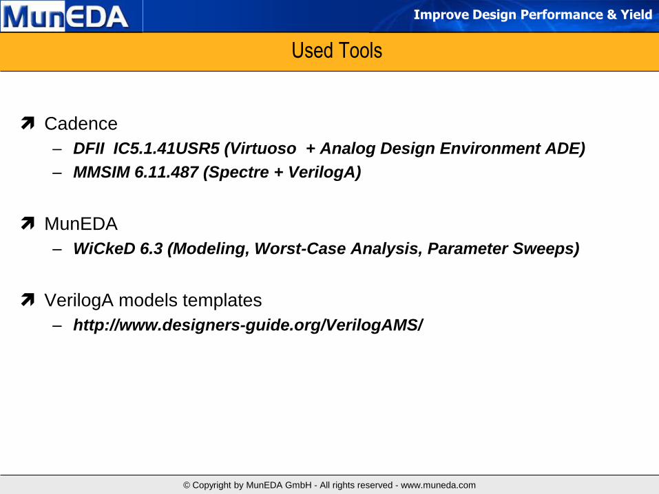
Cadence
– DFII IC5.1.41USR5 (Virtuoso + Analog Design Environment ADE)
– MMSIM 6.11.487 (Spectre + VerilogA)
MunEDA
– WiCkeD 6.3 (Modeling, Worst-Case Analysis, Parameter Sweeps)
VerilogA models templates
– http://www.designers-guide.org/VerilogAMS/
Improve Design Performance & Yield
© Copyright by MunEDA GmbH - All rights reserved - www.muneda.com
Overview
Introduction
– Motivation and Documented Use Cases
– Demonstrator: CP-PLL
– Starting Point
– Purpose
– Used tools
Block level
– Block Level Work Flow
– Frequency Divider Behavioral Model
– Phase Frequency Detector Behavioral Model
– Charge Pump Behavioral Model
– Voltage Controlled Oscillator Behavioral Model
CP-PLL
– Simulation setup
– Work flow
– Results
Improve Design Performance & Yield
© Copyright by MunEDA GmbH - All rights reserved - www.muneda.com
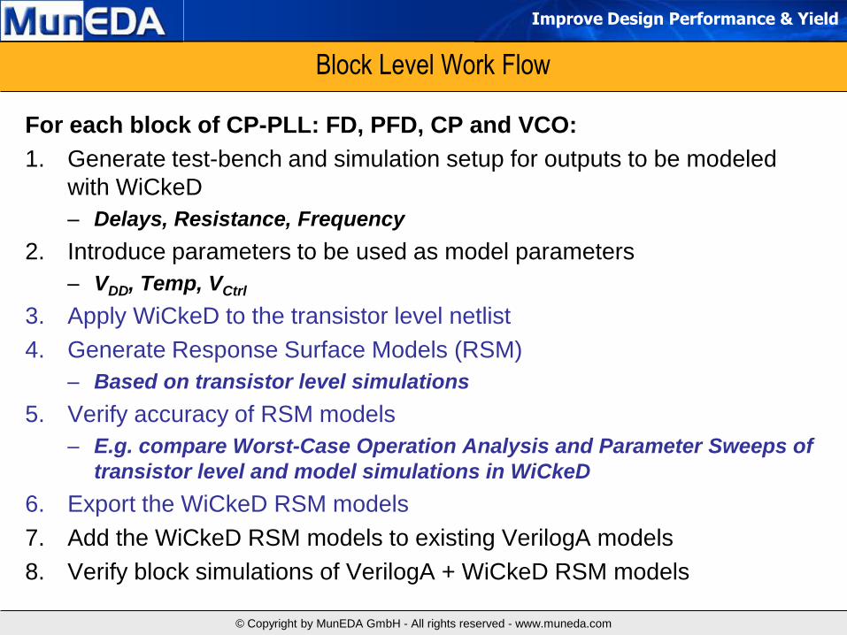
Block Level Work Flow
For each block of CP-PLL: FD, PFD, CP and VCO:
1. Generate test-bench and simulation setup for outputs to be modeled
with WiCkeD
– Delays, Resistance, Frequency
2. Introduce parameters to be used as model parameters
– VDD, Temp, VCtrl
3. Apply WiCkeD to the transistor level netlist
4. Generate Response Surface Models (RSM)
– Based on transistor level simulations
5. Verify accuracy of RSM models
– E.g. compare Worst-Case Operation Analysis and Parameter Sweeps of
transistor level and model simulations in WiCkeD
6. Export the WiCkeD RSM models
7. Add the WiCkeD RSM models to existing VerilogA models
8. Verify block simulations of VerilogA + WiCkeD RSM models
Improve Design Performance & Yield
© Copyright by MunEDA GmbH - All rights reserved - www.muneda.com
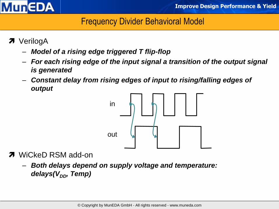
Frequency Divider Behavioral Model
VerilogA
– Model of a rising edge triggered T flip-flop
– For each rising edge of the input signal a transition of the output signal
is generated
– Constant delay from rising edges of input to rising/falling edges of
output
WiCkeD RSM add-on
– Both delays depend on supply voltage and temperature:
delays(VDD, Temp)
in
out
Improve Design Performance & Yield
© Copyright by MunEDA GmbH - All rights reserved - www.muneda.com
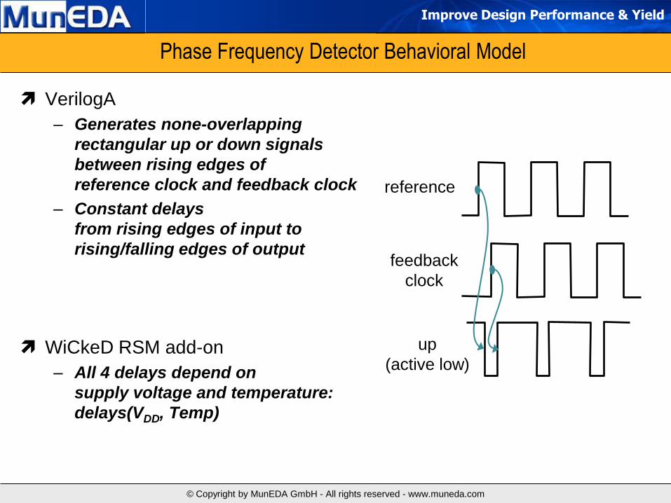
Phase Frequency Detector Behavioral Model
VerilogA
– Generates none-overlapping
rectangular up or down signals
between rising edges of
reference clock and feedback clock
– Constant delays
from rising edges of input to
rising/falling edges of output
WiCkeD RSM add-on
– All 4 delays depend on
supply voltage and temperature:
delays(VDD, Temp)
reference
feedback
clock
up
(active low)
Improve Design Performance & Yield
© Copyright by MunEDA GmbH - All rights reserved - www.muneda.com
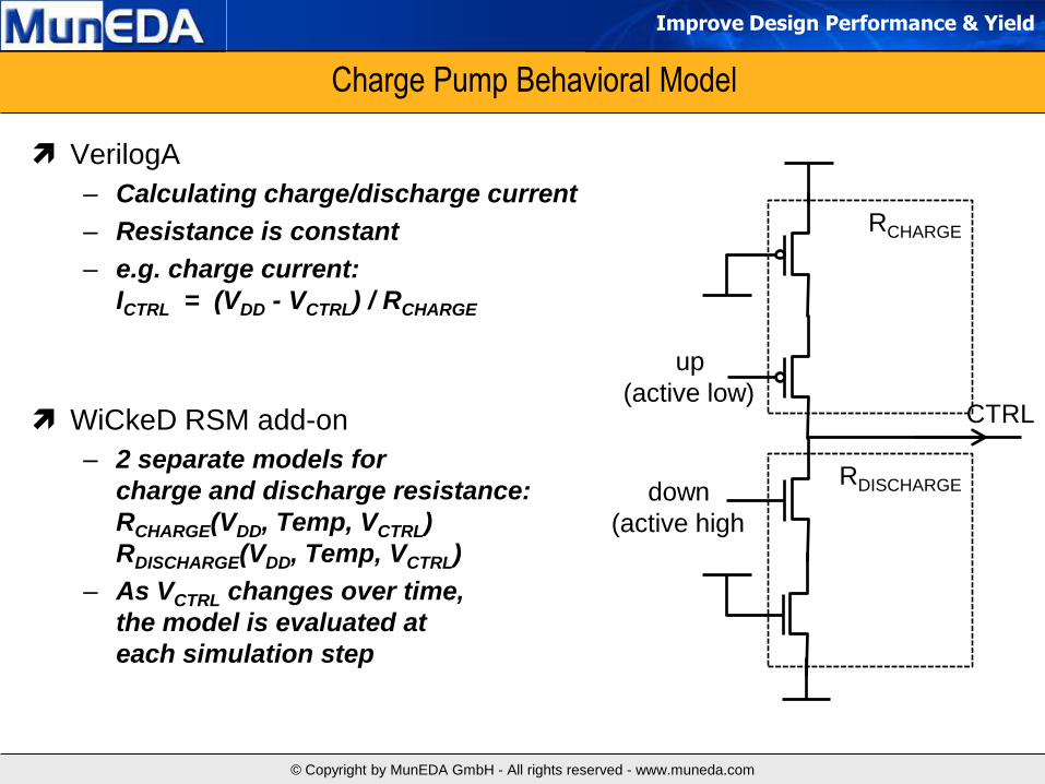
Charge Pump Behavioral Model
VerilogA
– Calculating charge/discharge current
– Resistance is constant
– e.g. charge current:
ICTRL = (VDD - VCTRL) / RCHARGE
WiCkeD RSM add-on
– 2 separate models for
charge and discharge resistance:
RCHARGE(VDD, Temp, VCTRL)
RDISCHARGE(VDD, Temp, VCTRL)
– As VCTRL changes over time,
the model is evaluated at
each simulation step
up
(active low)
down
(active high
RCHARGE
RDISCHARGE
CTRL
Improve Design Performance & Yield
© Copyright by MunEDA GmbH - All rights reserved - www.muneda.com
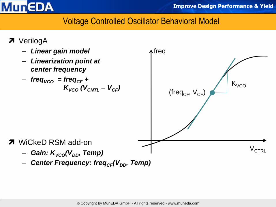
Voltage Controlled Oscillator Behavioral Model
VerilogA
– Linear gain model
– Linearization point at
center frequency
– freqVCO = freqCF +
KVCO (VCNTL – VCF)
WiCkeD RSM add-on
– Gain: KVCO(VDD, Temp)
– Center Frequency: freqCF(VDD, Temp)
KVCO
(freqCF, VCF)
freq
VCTRL

Improve Design Performance & Yield
© Copyright by MunEDA GmbH - All rights reserved - www.muneda.com
Overview
Introduction
– Motivation and Documented Use Cases
– Demonstrator: CP-PLL
– Starting Point
– Purpose
– Used tools
Block level
– Block Level Work Flow
– Frequency Divider Behavioral Model
– Phase Frequency Detector Behavioral Model
– Charge Pump Behavioral Model
– Voltage Controlled Oscillator Behavioral Model
CP-PLL
– Simulation setup
– Work flow
– Results
Improve Design Performance & Yield
© Copyright by MunEDA GmbH - All rights reserved - www.muneda.com
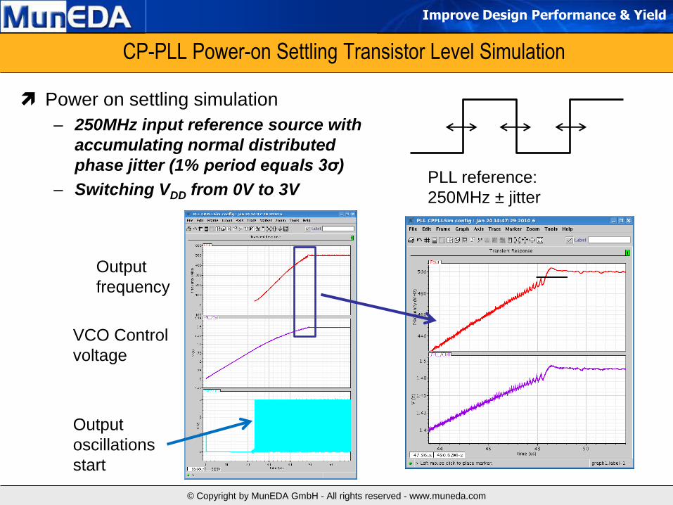
CP-PLL Power-on Settling Transistor Level Simulation
Power on settling simulation
– 250MHz input reference source with
accumulating normal distributed
phase jitter (1% period equals 3σ)
– Switching VDD from 0V to 3V PLL reference:
250MHz ± jitter
Output
oscillations
start
Output
frequency
VCO Control
voltage
Improve Design Performance & Yield
© Copyright by MunEDA GmbH - All rights reserved - www.muneda.com
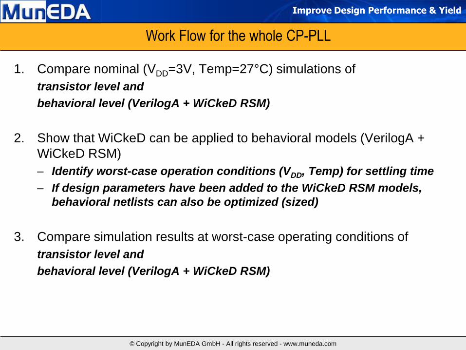
Work Flow for the whole CP-PLL
1. Compare nominal (VDD=3V, Temp=27°C) simulations of
transistor level and
behavioral level (VerilogA + WiCkeD RSM)
2. Show that WiCkeD can be applied to behavioral models (VerilogA +
WiCkeD RSM)
– Identify worst-case operation conditions (VDD, Temp) for settling time
– If design parameters have been added to the WiCkeD RSM models,
behavioral netlists can also be optimized (sized)
3. Compare simulation results at worst-case operating conditions of
transistor level and
behavioral level (VerilogA + WiCkeD RSM)
Improve Design Performance & Yield
© Copyright by MunEDA GmbH - All rights reserved - www.muneda.com
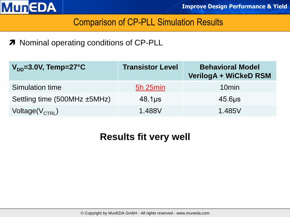
Comparison of CP-PLL Simulation Results
Nominal operating conditions of CP-PLL
Results fit very well
VDD=3.0V, Temp=27°C Transistor Level Behavioral Model
VerilogA + WiCkeD RSM
Simulation time 5h 25min 10min
Settling time (500MHz ±5MHz) 48.1μs 45.6μs
Voltage(VCTRL) 1.488V 1.485V
Improve Design Performance & Yield
© Copyright by MunEDA GmbH - All rights reserved - www.muneda.com
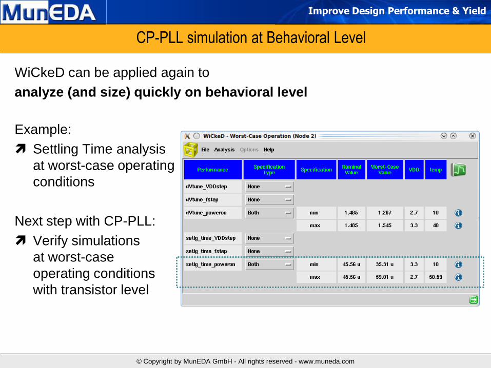
CP-PLL simulation at Behavioral Level
WiCkeD can be applied again to
analyze (and size) quickly on behavioral level
Example:
Settling Time analysis
at worst-case operating
conditions
Next step with CP-PLL:
Verify simulations
at worst-case
operating conditions
with transistor level
Improve Design Performance & Yield
© Copyright by MunEDA GmbH - All rights reserved - www.muneda.com
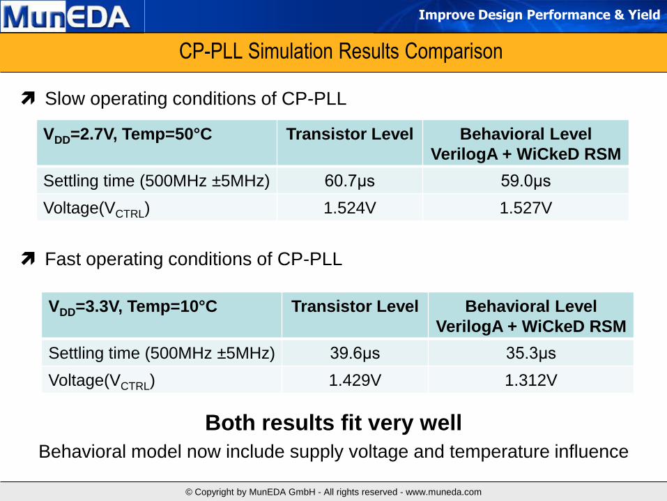
CP-PLL Simulation Results Comparison
Slow operating conditions of CP-PLL
Fast operating conditions of CP-PLL
Both results fit very well
Behavioral model now include supply voltage and temperature influence
VDD=2.7V, Temp=50°C Transistor Level Behavioral Level
VerilogA + WiCkeD RSM
Settling time (500MHz ±5MHz) 60.7μs 59.0μs
Voltage(VCTRL) 1.524V 1.527V
VDD=3.3V, Temp=10°C Transistor Level Behavioral Level
VerilogA + WiCkeD RSM
Settling time (500MHz ±5MHz) 39.6μs 35.3μs
Voltage(VCTRL) 1.429V 1.312V

Improve Design Performance & Yield
© Copyright by MunEDA GmbH - All rights reserved - www.muneda.com
Optimization Flow Úsing Behavioral Model(s)
To use behavioral models for all blocks of the CP-PLL in simulation:
1. Size each block at transistor level.
2. Create/update behavioral models for each block including selected
design parameters.
3. Size CP-PLL on the behavioral level.
4. Verify result w.r.t. transistor level.
To define block level specifications:
1. Start with a CP-PLL model at behavioral level
2. Optimize it (e.g. in nominal case)
3. Derive block specifications
4. Continue with the above flow and iteratively improve the design and
update specifications
Improve Design Performance & Yield
© Copyright by MunEDA GmbH - All rights reserved - www.muneda.com
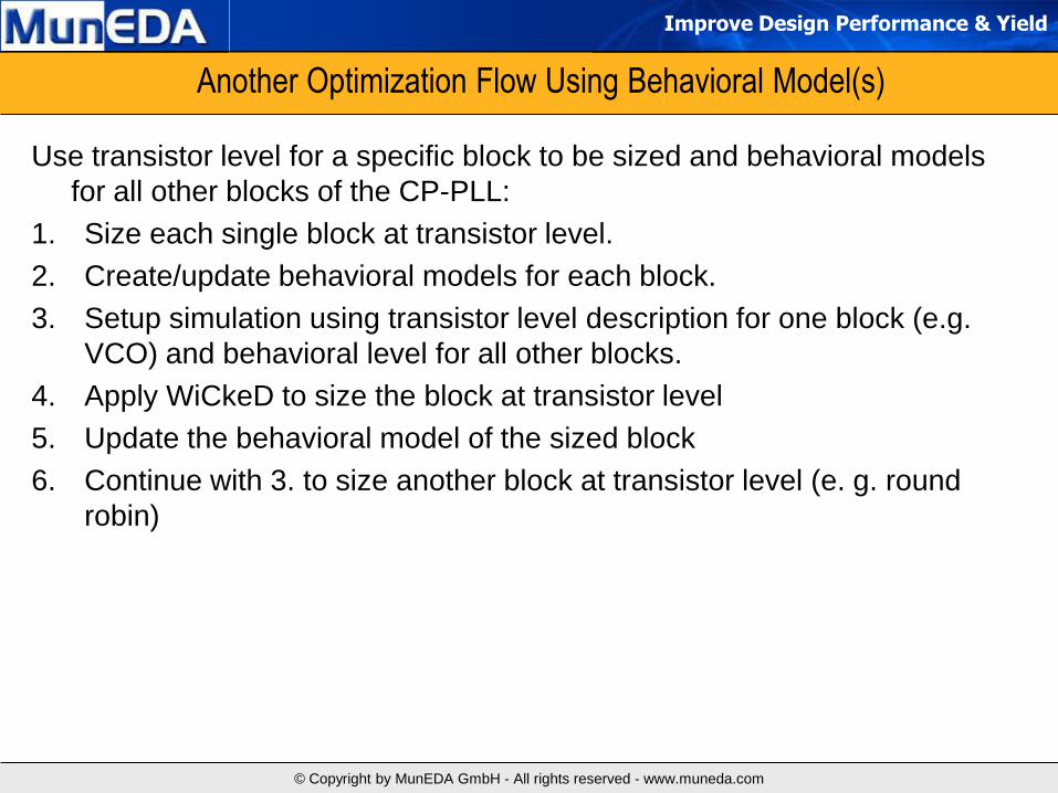
Another Optimization Flow Using Behavioral Model(s)
Use transistor level for a specific block to be sized and behavioral models
for all other blocks of the CP-PLL:
1. Size each single block at transistor level.
2. Create/update behavioral models for each block.
3. Setup simulation using transistor level description for one block (e.g.
VCO) and behavioral level for all other blocks.
4. Apply WiCkeD to size the block at transistor level
5. Update the behavioral model of the sized block
6. Continue with 3. to size another block at transistor level (e. g. round
robin)

Improve Design Performance & Yield
© Copyright by MunEDA GmbH - All rights reserved - www.muneda.com
Summary
We applied WiCkeD Modeling to speed up the simulation process of a
Charge Pump PLL.
Settling time was simulated. Input reference jitter can be simulated, as
well.
Simulation time was significantly reduced from 5h25m to 10m thanks to
VerilogA.
Behavioral simulation results well match transistor level simulation over
temperature and supply voltage thanks to WiCkeD RSM.
Possibility to apply WiCkeD to behavioral level netlists for sizing and
analysis.