Embed Size (px)
Citation preview
Parallel digital signal processing in a mW power
envelope: how and why?
Davide Rossi
DEI-UNIBOMultithermand AdG
Multiscale Thermal Management of Computing Systems

IOT or Data Deluge?
In-situ stream processing & fusion + visual intelligence is a must!
- In a few mW power envelope!!
Highly parallel workloads!
[Awaiba+Fraunhofer11]
4mW
CV is the energy bottleneck

How efficient?
3
[RuchIBM11]
1012ops/J
↓
1pJ/op
↓
1GOPS/mW

The challenge of
Energy Proportionality
4
From KOPS (103) to EOPS (1018)!
log(mW)
1GOPS/mW
log(GOPS)
0,003GOPS/mW – 30KW
0,04GOPS/mW

A Very Short Review on CMOS power and power minimization

Summary of Power Dissipation
Sources
a – switching activity
CL – load capacitance
CCS – short-circuit capacitance
Vswing – voltage swing
f – frequency
DDLeakDCDDswingCSL VIIfVVCCP a~
IDC – static current
Ileak – leakage current
powerstaticrateoperation
energyP
The Traditional Design Philosophy
Maximum performance is primary goal Minimum delay at circuit level
Architecture implements the required function
with target throughput, latency
Performance achieved through optimum sizing,
logic mapping, architectural transformations.
Supplies, thresholds set to achieve maximum
performance, subject to reliability constraints

The New Design Philosophy
Maximum performance (in terms of propagation delay) is
too power-hungry, and/or not even practically achievable
Many (if not most) applications either can tolerate larger
latency, or can live with lower than maximum clock-speeds
Excess performance (as offered by technology) to be used
for energy/power reduction
Trading off speed for power

In energy-constrained world, design is trade-off process
♦ Minimize energy for a given performance requirement
♦ Maximize performance for given energy budget
Delay
Unoptimized
design
DmaxDmin
Energy
Emin
Emax
Exploring the Energy-Delay Space
Pareto-optimal
designs
[Ref: D. Markovic, JSSC’04]

ASCI Springschool 2012 Henk Corporaal (10)
Reducing power @ all design levels
Algoritmic level
Compiler level
Architecture level
Organization level
Circuit level
Silicon level
Important concepts:
Lower Vdd and freq. (even if errors occur) /
dynamically adapt Vdd and freq.
Reduce circuit
Exploit locality
Reduce switching activity, glitches, etc.

ASCI Springschool 2012 Henk Corporaal (11)
Algoritmic level
The best indicator for energy is …..
…. the number of cycles
Try alternative algorithms with lower complexity
E.g. quick-sort, O(n log n) bubble-sort, O (n2)
… but be aware of the 'constant' : O(n log n) c*(n log n)
Heuristic approach
Go for a good solution, not the best !!
Biggest gains at this level !!

ASCI Springschool 2012 Henk Corporaal (12)
Compiler level
Source-to-Source transformations
loop trafo's to improve locality
Strength reduction
E.g. replace Const * A with Add's and Shift's
Replace Floating point with Fixed point
Reduce register pressure / number of accesses to register file
Use software bypassing
Scenarios: current workloads are highly dynamic
Determine and predict execution modes
Group execution modes into scenarios
Perform special optimizations per scenario
DFVS: Dynamic Voltage and Frequency Scaling
More advanced loop optimizations
Reorder instructions to reduce bit-transistions

ASCI Springschool 2012 Henk Corporaal (13)
Architecture level
Going parallel
Going heterogeneous
tune your architecture, exploit SFUs (special function
units)
trade-off between flexibility / programmability / genericity
and efficiency
Add local memories
prefer scratchpad i.s.o. cache
Cluster FUs and register files (see next slide)
Reduce bit-width
sub-word parallelism (SIMD)

ASCI Springschool 2012 Henk Corporaal (14)
Organization (micro-arch.) level
Enabling Vdd reduction
Pipelining
cheap way of parallelism
Enabling lower freq. lower Vdd
Note 1: don't pipeline if you don't need the performance
Note 2: don't exaggerate (like the 31-stage Pentium 4)
Reduce register traffic
avoid unnecessary reads and write
make bypass registers visible

ASCI Springschool 2012 Henk Corporaal (15)
Circuit level
Clock gating
Power gating
Multiple Vdd modes
Reduce glitches: balancing digital path's
Exploit Zeros
Special SRAM cells
normal SRAM can not scale below Vdd = 0.7 - 0.8 Volt
Razor method; replay
Allow errors and add redundancy to architectural invisible structures
branch predictor
caches
.. and many more ..

ASCI Springschool 2012 Henk Corporaal (16)
Silicon level
Higher Vt (V_threshold)
Back Biasing control see thesis Maurice Meijer (2011)
SOI (Silicon on Insulator) silicon junction is above an electr. insulator
(silicon dioxide)
lowers parasitic device capacitance
Better transistors: Finfet multi-gate
reduce leakage (off-state curent)
.. and many more

Two Ideas to Remember…with their caveats

Go Simple+Parallel
18
0
5
10
15
20
25
30
TPT One
App
Two
App
Four
App
Eight
App
Syste
m P
erf
orm
an
ce
Large
Med
Small
13mm, 100W, 48MB Cache, 4B Transistors, in 22nm
12 Cores 48 Cores 144 Cores
Single Core
Performance
1
0.5
0.3
0
0.2
0.4
0.6
0.8
1
1.2
La
rge
Me
d
Sm
all
Re
lati
ve
Pe
rfo
rma
nc
e
[S. Borkar, Intel, 2006]

Lower Voltage Supply
19
0.0
0.1
0.2
0.3
0.4
0.5
0.6
0.7
0.8
0.9
0.2 0.3 0.4 0.5 0.6 0.7 0.8 0.9 1 1.1 1.2
Total Energy
Leakage Energy
Dynamic Energy
0.55 0.55 0.55 0.55 0.6 0.7 0.8 0.9 1 1.1 1.2
En
erg
y/C
ycle
(nJ
)
32nm CMOS, 25oC
4.7X
Logic Vcc / Memory Vcc (V)
[V. De, Intel, 2013]
…but be careful with Leakage and its variability!

Introducing PULP

NTC Multicore?
1GOPS/mW
10x @10MOPSLeakage!
High Vdd
90nm LP-CMOS2010 - With EPFL (Atienza, Burg)

A pJ/OP Parallel ULP
Computing Platform
pJ/OP is traditionally* the target of ASIC + uCntr
Scalable: [KOPS,TOPS], 32bit architecture
Flexible: OpenMP, OpenVX
Open: Software & HW
22Departement Informationstechnologie und Elektrotechnik
*1.57TOPS/W: Kim et al., “A 1.22TOPS and 1.52mW/MHz Augmented Reality Multi-core Processor
with Neural Network NoC for HMD Applications”, ISSCC 2014

Making PULP
Integrated Systems Laboratory 23
Data
Memory
OpenRISC
Core #1
Instruction
Memory
Start with an simple+efficient processor (~1IPC)

Integrated Systems Laboratory 24
OpenRISC
Core #1
Instruction
Memory
OpenRISC
Core #2
Instruction
Memory
OpenRISC
Core #3
Instruction
Memory
OpenRISC
Core #N
Instruction
Memory
Data
Memory
Data
Memory
Data
Memory
Data
Memory
Parallel processors for performance @ NT
Making PULP
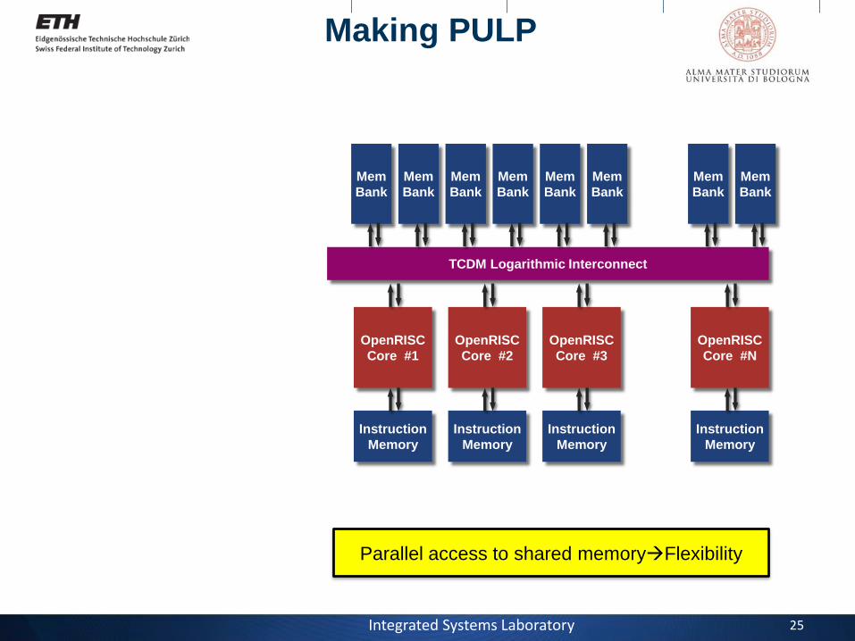
Integrated Systems Laboratory 25
TCDM Logarithmic Interconnect
OpenRISC
Core #1
Instruction
Memory
Mem
Bank
Mem
Bank
OpenRISC
Core #2
Instruction
Memory
Mem
Bank
Mem
Bank
OpenRISC
Core #3
Instruction
Memory
Mem
Bank
Mem
Bank
OpenRISC
Core #N
Instruction
Memory
Mem
Bank
Mem
Bank
Parallel access to shared memoryFlexibility
Making PULP

TCDM Logarithmic Interconnect
Integrated Systems Laboratory 26
OpenRISC
Core #1
Instruction
Memory
Mem
Bank
Mem
Bank
OpenRISC
Core #2
Instruction
Memory
Mem
Bank
Mem
Bank
OpenRISC
Core #3
Instruction
Memory
Mem
Bank
Mem
Bank
OpenRISC
Core #N
Instruction
Memory
Mem
Bank
Mem
Bank
Optional Instruction ExtensionAcceleration
Making PULP
EXU Logarithmic Interconnect
EXU #1 EXU #2 EXU #K

Integrated Systems Laboratory 27
L2
MemoryC
lus
ter
Bu
s
TCDM Logarithmic Interconnect
Cluster
Interface
Bus
Adapter
DMA
Instruction Bus
OpenRISC
Core #1
Instruction
Cache
Mem
Bank
Mem
Bank
OpenRISC
Core #2
Instruction
Cache
Mem
Bank
Mem
Bank
OpenRISC
Core #3
Instruction
Cache
Mem
Bank
Mem
Bank
OpenRISC
Core #N
Instruction
Cache
Mem
Bank
Mem
Bank
Add infrastructure to access off-cluster memory
Making PULP

Integrated Systems Laboratory 28
External
Interface
L3 Memory
High Speed Local Interconnect Bus
L
2
IF
1 2 3 N
Cluster 1
L
2
IF
1 2 3 N
Cluster 2
L
2
IF
1 2 3 N
Cluster M
Multiple clusters (f,Vdd,Vbb) form a PULP system
Making PULP

PULP Cluster
Design choices
I$ high code locality & simple architecture
No D$ low locality & high complexity: Bpmm2D$/Bpmm2
DTCDM<0,4
Sharing L1 less copies, easy work-balancing, low Tclk overhead in NT
Multibank smaller energy per access, “almost” multiported

OpenRisc Optimization
Superpipelining harmful for energy efficiency Focused speed optimization on the critical path dominated by MEM
Low pipeline depth high IPC with simple microarchitecture
(a) LD/ST, (b) MUL (c) BR
50% less energy per operation on average, 5% more area

Logarithmic Interconnect
P1 P2 P3 P4
B2
B3
B4
B5
B6
B7
B8
B1
Routing
Tree
Arbitration
Tree
Processors
Memory
Banks
N+1N N+2 N+3 N+4 N+5 N+6 N+7N+8
World-level bank interleaving «emulates» multiported mem
Ultra-low latency short wires + 1 clock cycle latency

Low latency
programming Interface Each command queue is dedicated to
a core of the cluster: arbitration is
made in hardware
No need to reserve (lock/unlock)
the programming channel
COREs program DMA through register
mapped on the DEMUX
The registers belongs to aliases,
no need for the processors to
calculate (per-core) offsets
A programming sequence requires1. check a free command queue
2. write address of buffer in TCDM
3. write address of buffer in L2 memory
4. Trigger data transfer
5. Synchronization
EXT ADDR
TCDM ADDR
CMD
TCDM ADDR
EXT ADDR
CMD
BUSYBUSY
Programming Latency: ~10 CLOCK CYCLES!!!

DMA Architecture Overview
33
CTRL UNIT: Arbitration – forwarding
and synchonization of incoming requests
TRANSFER UNIT: FIFO Buffers tor TX and
RX channnels
TCDM UNIT: Bridge to TCDM protocol –
4 channels (2 RD and 2 WR) 32 bit each
EXT UNIT: Bridge to AXI, 64 bit
Key idea: only channel packets buffered internally – no DMA transfers!

Cluster DMA
Maximum BW
for realistic
applications
BF = 2
Typical config

Sharing fucntional units
(instruction set extensions)
Private FPUPrivate FPU
-14
0%
-20
0%
Results normalized to
private FPU cfg
Results normalized to
private FPU cfg
-20
0%
-30
0%
SHARING FPUS
Floapint point units are area expensive, leakage hungry components
Typical FPU density in application is no more than 20%
FPUs typically feature latencies of several clock cycles

Scaling up
32 bit architecture
4 GB of memory
Clusters in Vdd, CLK
domains
L2 (2D & 3D) ready
Host VM IF for
Heterogeneous
Computing
17.07.2014 36
0x8000_0000
0xFFFF_FFFF
L3
Clust00x4000_0000
Clust10x4010_0000
Clust15
Clust0
0x3000_0000
Cluster
Peripherals0x2000_0000
Cluster
Memory0x1000_0000
0x0000_0000
0x4020_0000
0x41F0_0000
0x4200_0000
0x1000_0000
0x1080_0000
0x1F80_0000
0x2000_0000
Clust1
Clust15
0x4000_0000
0x5000_0000L2
Memory Map:

Programmability: OpenMP
while(1){
#pragma omp parallel num_threads(4){
#pragma sections{
#pragma section{
#pragma omp parallel num_threads(16)ColorScaleConv();
}#pragma section{
#pragma omp parallel num_threads(16)cvThreshold();
}#pragma section{
#pragma omp parallel num_threads(16)cvMoments();
}#pragma section{
#pragma omp parallel num_threads(16)cvAdd();
} }
}}
A.
C
EG
A
EE
B
EF
D
EH
C
EG
A
EE
B
EF
D
EH
B.
C.
D.
void ColorScaleConv(){
for(i = 0; i < FRAME_SIZE; i++){
[ALGORITH]}
}
#pragma omp for
A powerful abstraction for specifyingstructured parallelism
And very suitable for NUMA (cluster-based) systems
+OpenVX domain specific language
LLVM + OpenCL

Programming: OpenVX
• C-based standard API for vision kernel
Defines a set of standard kernels
Enables hardware vendors to implement
accelerated imaging and vision algorithms
• Focus on enabling real-time vision
On mobile and embedded systems
• Graph execution model
Each node can be implemented in software or
accelerated hardware
Data transfer between nodes may be optimized
Open source sample
implementation?
Hardware vendor implementations
OpenCV open
source library
Other higher-level
CV libraries
Application
OpenVXNode
OpenVXNode
OpenVXNode
OpenVXNode
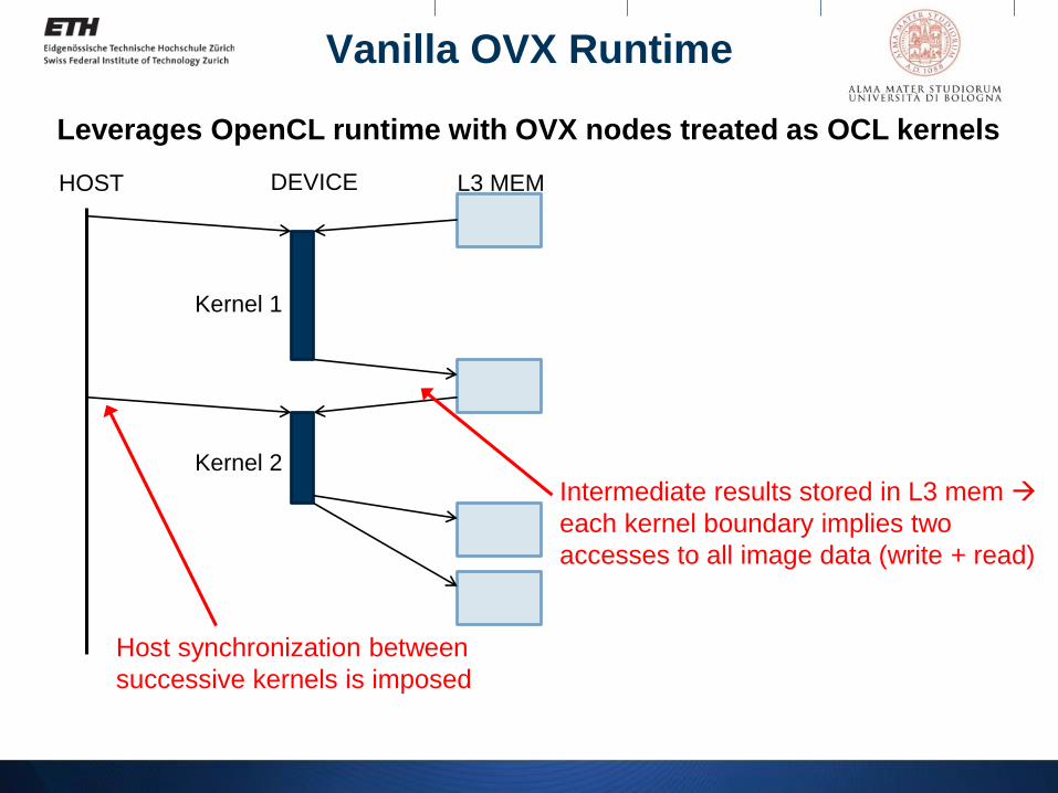
Vanilla OVX Runtime
HOST DEVICE L3 MEM
Kernel 1
Kernel 2
Leverages OpenCL runtime with OVX nodes treated as OCL kernels
Host synchronization between
successive kernels is imposed
Intermediate results stored in L3 mem
each kernel boundary implies two
accesses to all image data (write + read)

Localized Execution
TCDM is partitioned into 3 buffers (B0, B1, B2)
Output tile size is 160x120
Sobel3x3 requires image overlapping (1 pixel for each direction), and so the tile size
is 162x122
ColorConvert does not require tile overlapping, but must provide a 162x122 result tile
for the next stage → tile size propagation
Smaller image sub-regions (tiles) totally reside in TCDM
All kernels are computed at tile level, no more at image level → intermediate results are also allocated in TCDM

Localized Execution Results
• Framework prototype OpenVX support
A limited subset of kernel has been implemented
Polynomial time (i.e. fast) heuristics suitable for just-in-time execution
Cluster PE Efficiency

And what about Technology?

Near threshold FDSOI technology
44
Body bias: Highly effective knob for leakage control!

45Departement Informationstechnologie und Elektrotechnik
Near threshold FDSOI technology
PULP V1

PULP V1: Doing nothing well
(with RBB)
Peripheral
island
Ext island
Instruction Bus
IslandCore 0 : N-1 Islands Each processor can be
separately RBBed
depending on the
application workload
Handled at software level
through nested creation /
destruction of threadsTCDM 0: M-1 Islands Each TCDM bank can be separately switched off depending on the application’s memory footprint
Requires reconfiguration of TCDM interconnect addressing scheme
Requires re-allocation of stack and program data after each reconfiguration
TCDM
Interconnect
Island
State-Retentive + Low Leakage + Fast transitions
More than 50% of power into memories… this is the next focus area!
0.2mm2
0.4-1.3V
28nm FDSOI

Introducing PULP V2

Board/Application-ready chip
Implementation of a master
and a slave peripheral
Standard peripheral (e.g. SPI)
Integration with FPGAs or
standard low power external
memories
PULP as multi-core
accelerator for micro-
controller host
STM32 host core
PULP muti-core accelerator
Daisy chain of PULP chips
Pipeline of parallel processing
units
Each core perfrorms a stage of
computation and forword
temporary data to another stage
48
Standalone mode is also supported!

Clock generator: FLL
All-digital clock generation based on a Frequency Lock Loop (FLL)
From 2GHz down to 15KHz (through clock division)
Frequency step 10MHz (at lowest division factor)
Small area 3300µm² (50 times smaller than classic PLL)
Suited to fine-grain GALS architectures
Frequency reprograming in less than 180ns
No frequency overshoot
15ps jitter
ControllerTarget
frequency
DCO
DAC+- VCO
Frequency counter
Clock divider
Clk_ref
Clk_out
Division factor
N
S. Lesecq, D. Puschini, E. Beigne, P. Vivet, and Y. Akgul, “Low-Cost and Robust Control of a DFLL for Multi-Processor System-on-Chip,”
IFAC Proceedings Volumes, vol. 18, pp. 1940–1945, 2011

50Departement Informationstechnologie und Elektrotechnik
Near threshold FDSOI technology
PULP V1
PULP V2
Low-leakage vs. Low voltage (0.3V) reactive or proactive?

ULP Latch-based SCM
Based exclusively on standard cells
Voltage range identical to the core Only static logic
Layout based on guided P&R Close to 100% density
51
64 words x 64 bit
162 x 85 =
13.7k um2
Decoders
Storage
Array +
output muxMacro Size:
128 x 32 (4 kb)
86μm x 160μm
Input/Output Delay:
0.3ns/0.7ns @ss0.9V125°2ns/3.3ns @tt0.3V25°(FBB)
SCMs

Comparison to 64x64 SRAM
52

SCM Integration into PULP2
53
16 banks of
128x32 bit SCM
(8 kbyte)
2 banks of
128x32 bit SCM
(2 kbyte)
Instruction
cache per core
8 banks of
512x32 bit SRAM
(16 kbyte)
PULP V2 is taping out this Week, PULP V3 is on the drawing board…

Bank 1 Bank x
Reconfigurable address mapping
Support for different address
mappings: Interleaved: horizontal shutdown and
reduces conflicts in shared segments
Non-interleaved mapping: private memory avoids conflicts
Basic MMU Coexistence of both shared and
private memory segments with different address mappings
Adapt address mapping is adapted to accommodate partial memory shut-down
54
Bank 0
...
MMU
priva
tesh
are
d
Mapping between logical-
physical addresses
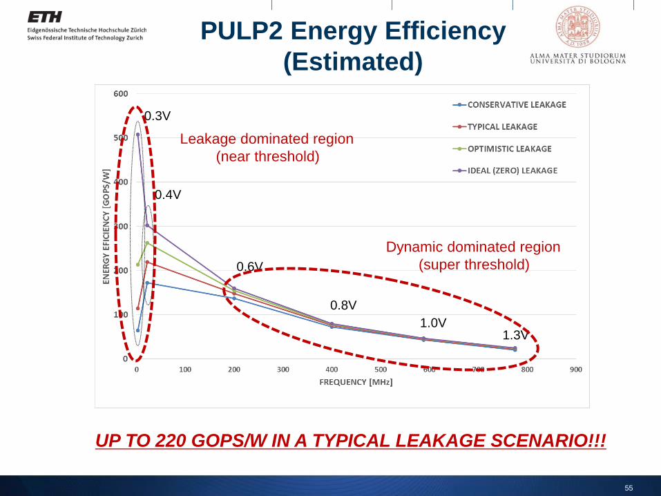
PULP2 Energy Efficiency
(Estimated)
55
0.3V
0.4V
0.6V
0.8V
1.0V1.3V
Leakage dominated region
(near threshold)
Dynamic dominated region
(super threshold)
UP TO 220 GOPS/W IN A TYPICAL LEAKAGE SCENARIO!!!

Introducing FBB...
56
Leakage power gowth
much more than frequency
Almost no impact on dynamic power,
Leakage is negligible
UP TO 1.5X ENERGY EFFICIENCY FOR HIGH WORKLOADS!!!
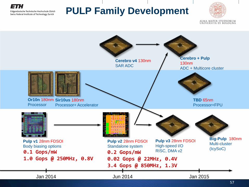
Pulp v1 28nm FDSOI
Body biasing options
Pulp v2 28nm FDSOI
Standalone system
Pulp v3 28nm FDSOI
High-speed I/O
RISC, DMA v2
Big-Pulp 180nm
Multi-cluster
(IcySoC)
PULP Family Development
Jan 2014 Jun 2014 Jan 2015
Sir10us 180nm
Processor+ Accelerator
Or10n 180nm
ProcessorTBD 65nm
Processor+FPU
Cerebro v4 130nm
SAR ADC
Cerebro + Pulp
130nm
ADC + Multicore cluster
57
0.2 Gops/mW0.02 Gops @ 22MHz, 0.4V3.4 Gops @ 850MHz, 1.3V
0.1 Gops/mW1.0 Gops @ 250MHz, 0.8V

An ULP Computing Ecosystem
What do we need to put together a
«computing platform»?
HARDWARE IPs PROCESSOR
INTERCONNECT (LOCAL, GLOBAL)
MEMORY HIERARCHY (CACHES,
MEMORY CONTROLLERS
HARDWARE ACCELERATORS
…
SOFTWARE COMPILER/TOOLCHAIN
PROGRAMMING MODELS
RUNTIME
…
VALIDATION VIRTUAL PLATFORM
EMULATION PLATFORM
(FPGA)
BENCHMARKS
REGRESSION TESTS
…
SILICON OPTIMIZATION FLOW
IMPLEMENTATION FLOW
VERIFICATION FLOW
FULL CUSTOM IPS
…
BUT ALSO… SUPPORT FOR DEBUG
SUPPORT FOR PROFILING
DESIGN FOR TESTABILITY
…..
Building an open-
source ecosystem for
exploring (with silicon!)
next-generation parallel
computing platforms

To do what?
59
112x112pixel (300uW)
@60fps 0.76MPx/s with 1KOPS/pixel we need 0.75Gops!
[Wood13]
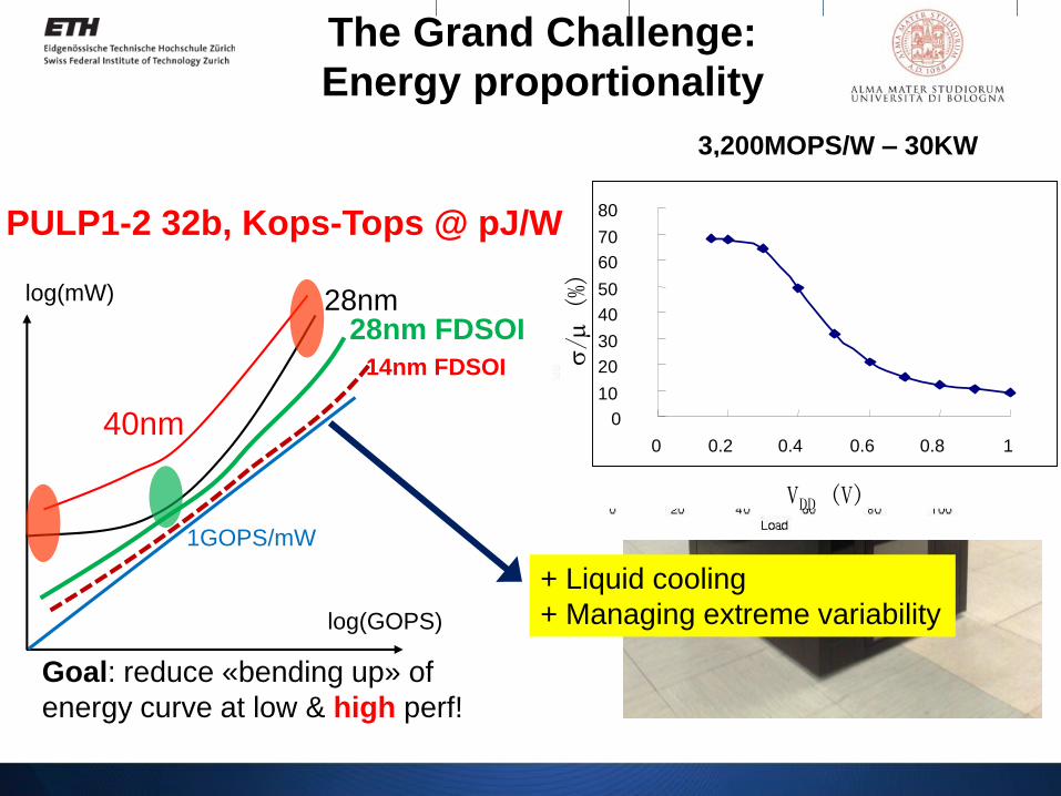
log(mW)
1GOPS/mW
28nm
40nm
log(GOPS)
28nm FDSOI
14nm FDSOI
Goal: reduce «bending up» of
energy curve at low & high perf!
The Grand Challenge:
Energy proportionality
3,200MOPS/W – 30KW
+ Liquid cooling
+ Managing extreme variability
0
10
20
30
40
50
60
70
80
0 0.2 0.4 0.6 0.8 1
VDD (V)
/(%)
PULP1-2 32b, Kops-Tops @ pJ/W

Multithermand AdG
Multiscale Thermal Management of Computing Systems