Embed Size (px)
Citation preview

Parallel Communications PCIe
Last updated – 4/6/20

2 © tjEE 4980 – MES
PCIE• PCIe
• Peripheral Component Interconnect - Express
• Preceded by PCI and PCI-X• But completely different physically
• Logical configuration separate from the physical configuration• Logical configuration is backward compatible → SW reuse
• On-chip or on-board
• Packet based – point to point architecture

3 © tjEE 4980 – MES
PCIE
• PCIe
• Point to point• Fixed – hardwired direct connection (LINK)

4 © tjEE 4980 – MES
PCIE
• PCIe
• Why point to point?
• Reduces the RC delay on the signals
• Allows for very fast transfer speeds
• 2.5GT/s, 5GT/s, 8GT/s, 16GT/s, 32GT/s with 64GT/s in 2021• GT/s – Giga-Transfers per second
• Assumes simultaneous Rx/Tx

5 © tjEE 4980 – MES
PCIE
• PCIe
• Networked - uses switches to route messages

6 © tjEE 4980 – MES
PCIE
• PCIe
• Lane• 1 transmit path and 1 receive path
• Differential signaling → 4 wires/Lane
• Link• Collection of Lanes
• 1x, 2x, 4x, 8x, 12x, 16x, 32x
• Symmetric – same both directions
• No Clock !

7 © tjEE 4980 – MES
PCIE
• PCIe• Lanes and Links
PCI Expressversion
IntroducedLinecode
Transferrate[i]
Throughput[i]
x1 x2 x4 x8 x16
1.0 2003 8b/10b 2.5 GT/s 250 MB/s 0.500 GB/s 1.00 GB/s 2.0 GB/s 4.0 GB/s
2.0 2007 8b/10b 5.0 GT/s 500 MB/s 1.000 GB/s 2.00 GB/s 4.0 GB/s 8.0 GB/s
3.0 2010 128b/130b 8.0 GT/s 984.6 MB/s 1.969 GB/s 3.94 GB/s 7.88 GB/s 15.75 GB/s
4.0 2017 128b/130b 16.0 GT/s 1969 MB/s 3.938 GB/s 7.88 GB/s 15.75 GB/s 31.51 GB/s
5.0 2019 128b/130b 32.0 GT/s[ii] 3938 MB/s 7.877 GB/s 15.75 GB/s 31.51 GB/s 63.02 GB/s
6.0 (planned)
2021 128b/130b 64.0 GT/s 7877 MB/s 15.754 GB/s 31.51 GB/s 63.02 GB/s 126.03 GB/s
But wait !
5GT/s x 8 links = 40GT/s
40GT/s / 8 bits = 5GB/s
Why the difference?
8 © tjEE 4980 – MES
PCIE
• PCIe
• Encoding• PCIe 1.x and 2.x use 8b/10b encoding
• PCIe 3.x - 6.x use 128b/130b encoding
• 8b/10b Encoding• Maps 8 bit symbols to 10 bit symbols
• Coding ensures # of 1s and # of 0s differ by ≤ 2 for any string of 20 bits
• Coding ensures no more than 5, 0s or 1s in a row
• Provides enough transitions to do clock recovery
• Provides for DC balance

9 © tjEE 4980 – MES
PCIE
• PCIe signaling
• Clock Recovery
• Both Rx and Tx generate a common clock frequency• 2.5Ghz, 5GHz, 8GHz, 16GHz
• Only at the Rx/Tx interfaces
• Phase between Rx and Tx is uncorrelated
• Rx side uses a PLL to phase align the receiver clock to the incoming differential signal• This is where encoding helps – ensures sufficient transitions to keep
PLL locked

10 © tjEE 4980 – MES
PCIE
• PCIe signaling
src: design reuse

11 © tjEE 4980 – MES
PCIE
• PCI Layering
12 © tjEE 4980 – MES
PCIE
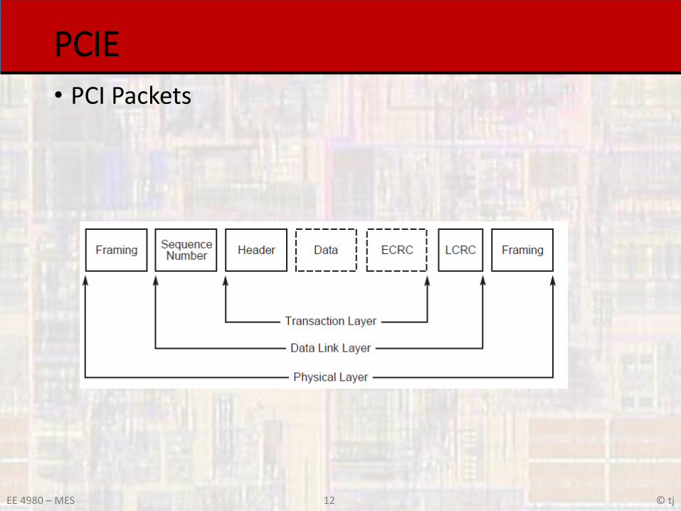
• PCI Packets

13 © tjEE 4980 – MES
PCIE• Primary Functional Blocks
• Root Complex• Endpoint• Switch• Bridge
• Upstream Port (only 1) - points toward the root complex• Downstream Port(s) – point away from root complex
• Ingress Port – incoming port (receiver)• Egress Port – outgoing port (transmitter)

14 © tjEE 4980 – MES
PCIE
• Root Complex
• Connects CPU(s) and Memory to the PCI fabric
• Multiple PCIe ports
• Generates transactions based on commands from the CPU
• Can act as power controller, interrupt controller, error detection response
15 © tjEE 4980 – MES
PCIE
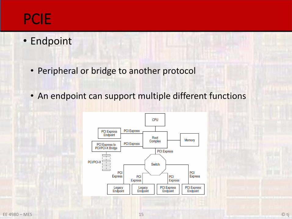
• Endpoint
• Peripheral or bridge to another protocol
• An endpoint can support multiple different functions

16 © tjEE 4980 – MES
PCIE• Switch
• Acts like multiple virtual bridges – PCIe to PCIe
• Hierarchy of bridges allowed
• Configuration includes information on• Downstream devices• Downstream buses
• Forwards based on• Address routing• ID routing• Implicit routing• Up one level, root device, …

17 © tjEE 4980 – MES
PCIE
• Switch – cont’d
• Perform port arbitration• Multiple transactions to the same port
• Perform Virtual Channel arbitration• Priority decisions
18 © tjEE 4980 – MES
PCIE
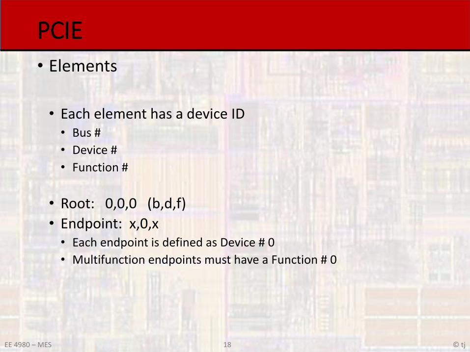
• Elements
• Each element has a device ID• Bus #
• Device #
• Function #
• Root: 0,0,0 (b,d,f)
• Endpoint: x,0,x• Each endpoint is defined as Device # 0
• Multifunction endpoints must have a Function # 0

19 © tjEE 4980 – MES
PCIE
• Transactions
• Transaction• 1 or more packet transmissions
• Each transaction has a Tag associated with it• Allows split transactions

20 © tjEE 4980 – MES
PCIE
• Transactions
• Non-posted transaction• A response is expected at some future time
• E.g. memory read
• Posted transaction• No response is required or expected
• E.g. non-posted memory write
• Requesters and Completers instead of Master/slave

21 © tjEE 4980 – MES
PCIE
• Multi-Layer Protocol
• Transaction Layer
• Data Layer
• Physical Layer
• TLP • Transaction Layer Packet
• Originates/terminates at the Transaction Layer
• DLLP • Data Link Layer Packet
• Originates/terminates at the Data Link Layer

22 © tjEE 4980 – MES
PCIE
• Multi-Layer Protocol

23 © tjEE 4980 – MES
PCIE
• Transaction Layer
• Creates TLPs
• Interfaces to the peripheral to make requests or provide results• Read – address, device, …
• Write – address, device, data
• Flow control• Buffer overflow, underflow
• Each packet has a unique identifier
• Where the Memory, IO, Config and Messages are created and consumed

24 © tjEE 4980 – MES
PCIE
• Data Link Layer
• Takes packet info from the Transaction Layer, adds to it, and transmits to the Physical Layer – and reverse
• Provides Link Management• Supports data integrity• Error detection & correction
• Requests re-transmits
• Creates and uses packets for link management separate from transferring Transaction Layer information (DLLPs)

25 © tjEE 4980 – MES
PCIE
• Physical Layer
• Separated into two sections
• Logical• Formats data
• Adds framing information
• Electrical• RX/TX circuitry

26 © tjEE 4980 – MES
PCIE
• Transaction Layer Packets
• Left most bit transferred first

27 © tjEE 4980 – MES
PCIE
• Transaction Layer Packets
• Left most bit transferred first

28 © tjEE 4980 – MES
PCIE
• Transaction Layer Packets
• Header portion

29 © tjEE 4980 – MES
PCIE
• Transaction Layer Packets• Header portion

30 © tjEE 4980 – MES
PCIE
• Transaction Layer Packets
• Header portion

31 © tjEE 4980 – MES
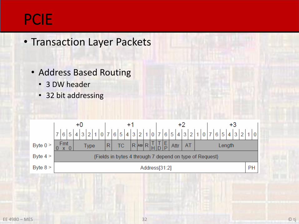
PCIE
• Transaction Layer Packets
• Address Based Routing• 4 DW header
• 64 bit addressing
32 © tjEE 4980 – MES
PCIE
• Transaction Layer Packets
• Address Based Routing• 3 DW header
• 32 bit addressing

33 © tjEE 4980 – MES
PCIE
• Transaction Layer Packets
• ID Based Routing

34 © tjEE 4980 – MES
PCIE
• Transaction Layer Packets
• Data Word Byte Enable
• Provides Byte level enabling of the first and last data words
• All intermediate words (assuming >2 for length) must match both the first and last DW enable
• 32 bit words → 4 bytes
• 1st DWenable = 0110, last DWenable = 1100• Enable byte 1 and 2 of the 1st word, no intermediate words, bytes 2 and
3 of the last DW

35 © tjEE 4980 – MES
PCIE
• Transaction Layer Packets
• Transaction ID• Requester ID
• Tag
• Attributes – no-snoop?
• Transaction class – best effort, round robin, …

36 © tjEE 4980 – MES
PCIE
• Transaction Layer Packets
• IO Transaction Request Example

37 © tjEE 4980 – MES
PCIE
• Transaction Layer Packets
• Configuration Transaction Request Example

38 © tjEE 4980 – MES
PCIE
• Transaction Layer Packets
• Completion header• Header for any completion packets
• E.g. results of a read

39 © tjEE 4980 – MES
PCIE
• Transaction Layer Packets
• Optional Digest Field• Can be used for additional data checking at the Transaction Layer
• Use a CRC – Cyclical Redundancy Check on the bits of the Transaction Layer Packet
40 © tjEE 4980 – MES
PCIE
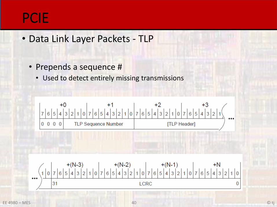
• Data Link Layer Packets - TLP
• Prepends a sequence #• Used to detect entirely missing transmissions
• Appends a CRC

41 © tjEE 4980 – MES
PCIE
• Data Link Layer Packets - DLLP
• General format

42 © tjEE 4980 – MES
PCIE
• Data Link Layer Packets - DLLP
• General format
• Ack/Nak format

43 © tjEE 4980 – MES
PCIE
• Physical Layer – Logical
• Framing

44 © tjEE 4980 – MES
PCIE
• Physical Layer – Logical
• Framing Token – Start of TLP

45 © tjEE 4980 – MES
PCIE
• Physical Layer – Logical
• Striping

46 © tjEE 4980 – MES
PCIE
• Packet example

47 © tjEE 4980 – MES
PCIE
• Physical Layer - Logical
• Encoding• PCIe 1.x and 2.x use 8b/10b encoding
• PCIe 3.x and 4.x use 128b/130b encoding
• 8b/10b Encoding• Maps 8 bit symbols to 10 bit symbols
• Coding ensures # of 1s and # of 0s differ by ≤ 2 for any string of 20 bits
• Coding ensures no more than 5, 0s or 1s in a row
• Provides enough transitions to do clock recovery
• Provides for DC balance

48 © tjEE 4980 – MES
PCIE
• Physical Layer - Logical
• 8b/10b Encoding• Bottom 5 bits → 6 bit code
5b/6b code
Input RD = −1 RD = +1 Input RD = −1 RD = +1
EDCBA abcdei EDCBA abcdei
D.00 00000 100111 011000 D.16 10000 011011 100100
D.01 00001 011101 100010 D.17 10001 100011
D.02 00010 101101 010010 D.18 10010 010011
D.03 00011 110001 D.19 10011 110010
D.04 00100 110101 001010 D.20 10100 001011
D.05 00101 101001 D.21 10101 101010
D.06 00110 011001 D.22 10110 011010
D.07 00111 111000 000111 D.23 † 10111 111010 000101
D.08 01000 111001 000110 D.24 11000 110011 001100
D.09 01001 100101 D.25 11001 100110
D.10 01010 010101 D.26 11010 010110
D.11 01011 110100 D.27 † 11011 110110 001001
D.12 01100 001101 D.28 11100 001110
D.13 01101 101100 D.29 † 11101 101110 010001
D.14 01110 011100 D.30 † 11110 011110 100001
D.15 01111 010111 101000 D.31 11111 101011 010100
K.28 11100 001111 110000

49 © tjEE 4980 – MES
PCIE
• Physical Layer - Logical
• 8b/10b Encoding• Top 3 bits → 4 bit code
3b/4b code
InputRD = −1
RD = +1
InputRD = −1
RD = +1
HGF fghj HGF fghj
D.x.0 000 1011 0100 K.x.0 000 1011 0100
D.x.1 001 1001 K.x.1 ‡ 001 0110 1001
D.x.2 010 0101 K.x.2 ‡ 010 1010 0101
D.x.3 011 1100 0011 K.x.3 ‡ 011 1100 0011
D.x.4 100 1101 0010 K.x.4 100 1101 0010
D.x.5 101 1010 K.x.5 ‡ 101 0101 1010
D.x.6 110 0110 K.x.6 ‡ 110 1001 0110
D.x.P7 †
111 1110 0001
D.x.A7 †
111 0111 1000 K.x.7 † 111 0111 1000

50 © tjEE 4980 – MES
PCIE
• Physical Layer – Logical
• Symbol Encoding

51 © tjEE 4980 – MES
PCIE
• Physical Layer

52 © tjEE 4980 – MES
PCIE
• PCIe signaling
• 2 wires for each transmission
• Differential signals• Differential receivers and transmitters
• AC coupled → different levels at each end• How do we do this ?
• Differential Pk-Pk voltages from 800mv to 1.2v
• + Vpp → 1 -Vpp → 0
• Common mode range from 0 to 3.6v

53 © tjEE 4980 – MES
PCIE
• PCIe signaling
• LVDS – Low Voltage Differential Signalling