Embed Size (px)
DESCRIPTION
AES
Citation preview

Parallel AES Encryption Enginesfor Many-Core Processor Arrays
Bin Liu, Student Member, IEEE, and Bevan M. Baas, Senior Member, IEEE
Abstract—By exploring different granularities of data-level and task-level parallelism, we map 16 implementations of an Advanced
Encryption Standard (AES) cipher with both online and offline key expansion on a fine-grained many-core system. The smallest design
utilizes only six cores for offline key expansion and eight cores for online key expansion, while the largest requires 107 and 137 cores,
respectively. In comparison with published AES cipher implementations on general purpose processors, our design has 3.5-15.6 times
higher throughput per unit of chip area and 8.2-18.1 times higher energy efficiency. Moreover, the design shows 2.0 times higher
throughput than the TI DSP C6201, and 3.3 times higher throughput per unit of chip area and 2.9 times higher energy efficiency than
the GeForce 8800 GTX.
Index Terms—Advanced encryption standard (AES), AsAP, fine-grained, many-core, parallel processor, software, synchronous
dataflow
Ç
1 INTRODUCTION
WITH the development of information technology,protecting sensitive information via encryption is
becoming more and more important to daily life. In 2001,the National Institute of Standards and Technology (NIST)selected the Rijndael algorithm as the Advanced EncryptionStandard (AES) [1], which replaced the Data EncryptionStandard (DES) [2]. Since then, AES has been widely used in avariety of applications, such as secure communicationsystems, high-performance database servers, digital video/audio recorders, RFID tags, and smart cards.
To satisfy different applications’ requirements, numeroushardware implementations of AES have been reported.Verbauwhede et al. described the first AES implementationon silicon, which can provide a 2.29 Gbps throughput with anonpipeline architecture [3]. Mukhopadhyay and Roy-Chowdhury improved their AES system to 8 Gbps withpipelining [4], which is a common technique used to enhancethe performance of a system [5]. The first AES implementa-tion with a throughput over 10 Gbps was proposed byapplying T-box [6], which is a combination of the SubBytes,ShiftRows, and MixColumns phases in the AES algorithm [7].Furthermore, the area-throughput tradeoffs of fully pipe-lined AES processors with throughputs between 30 and70 Gbps have been presented [8]. Recently, Mathew et al.implemented a 53 Gbps AES accelerator in 45 nm CMOStechnology [9]. Besides application specific integrated circuit(ASIC) designs, configurable hardware is another choice forAES implementations. For example, there are several FPGAimplementations that achieve a throughput approximately
20 to 30 Gbps [10], [11], [12] by applying loop unrolling and
pipelining. Recently, Qu et al. demonstrated a 73.7 Gbps AES
system on a Xilinx XC5VLX85 chip running at 570 MHz [13].Although hardware implementations generally offer
higher throughput and better energy efficiency than soft-
ware designs, they are difficult to upgrade and adapt for
future possible protocol changes. Moreover, ASIC designs
are very time consuming and costly. For example, it takes
generally 18 to 24 months for a full custom ASIC product
and costs approximately 50 Million USD to design [14]. One
advantage of the Rijndael algorithm is that it is not only fit
for hardware implementations, but also suitable for efficient
software designs. Matsui and Nakajima proposed a bitslice
AES implementation on Intel Core 2, which achieves a
9.2 clock cycles per byte throughput for a data chunk longer
than 2,048 bytes, equaling 1.85 Gbps when the core is
running at its maximum frequency of 2.13 GHz [15]. The
bitslice technique was first proposed by Biham for fast DES
implementation on a software platform with a word size
longer than 16 bits [16]. Bernstein and Schwabe investigated
the opportunities of reducing instruction count and cycles
by combining different instructions together for various
architectures [17]. Both bitslice and specific sets of instruc-
tions from Supplemental Streaming SIMD Extensions 3
(SSSE3 [18]) are utilized to enhance the performance of Intel
Core i7 920 as high as 6.92 clock cycles per byte [19]. Besides
pure general software AES implementations, the Intel AES-
NI utilizes specialized hardware to support six AES
instructions, and achieves a throughput of 1.28 clock cycles
per byte [20]. There is also a trend to use Graphic Processing
Units (GPUs) and DSP processors to implement the AES
algorithm. Wollinger et al. compared different encryption
algorithms on a TMS320C6X processor and achieved a
14.25 clock cycles per byte [21]. Manavski presented an AES
implementation with a peak throughput of 8.28 Gbps on a
GeForce 8,800 GTX chip when the input data block is longer
than 8 MB [22].
536 IEEE TRANSACTIONS ON COMPUTERS, VOL. 62, NO. 3, MARCH 2013
. The authors are with the Department of Electrical and ComputerEngineering, University of California, Davis, CA 95616.E-mail: {binliu, bbaas}@ucdavis.edu.
Manuscript received 15 Aug. 2011; revised 18 Nov. 2011; accepted 6 Dec.2011; published online 22 Dec. 2011.Recommended for acceptance by J. Plusquellic.For information on obtaining reprints of this article, please send e-mail to:[email protected], and reference IEEECS Log Number TC-2011-08-0546.Digital Object Identifier no. 10.1109/TC.2011.251.
0018-9340/13/$31.00 � 2013 IEEE Published by the IEEE Computer Society

This paper presents various software implementations ofthe AES algorithm with different data and task parallelismgranularity, and shows that AES implementations on a fine-grained many-core system can achieve high performance,throughput per unit of chip area and energy efficiencycompared to other software platforms. Both the online andoffline key expansion process for each implementationmodel are discussed. The reminder of this paper isorganized as follows: Section 2 introduces the AES algo-rithm. Section 3 briefly describes the features of the targetedfine-grained many-core system. In Section 4, variousimplementations are analyzed by synchronous dataflow(SDF) models, mapped and measured on the targetedplatform. Section 5 presents the area optimization metho-dology and compares the area efficiency among differentimplementations. Section 6 compares the energy efficiency.Section 7 compares our work with other software designs.Finally, Section 8 concludes the paper.
2 ADVANCED ENCRYPTION STANDARD
AES is a symmetric encryption algorithm, and it takes a128-bit data block as input and performs several rounds oftransformations to generate output ciphertext. Each 128-bitdata block is processed in a 4-by-4 array of bytes, called thestate. The round key size can be 128, 192 or 256 bits. The numberof rounds repeated in the AES,Nr, is defined by the length ofthe round key, which is 10, 12 or 14 for key lengths of 128, 192 or256 bits, respectively. Fig. 1 shows the AES encryption stepswith the key expansion process. For encryption, there are fourbasic transformations applied as follows:
1. SubBytes: The SubBytes operation is a nonlinear bytesubstitution. Each byte from the input state isreplaced by another byte according to the substitu-tion box (called the S-box). The S-box is computedbased on a multiplicative inverse in the finite fieldGF(28) and a bitwise affine transformation.
2. ShiftRows: In the ShiftRows transformation, the firstrow of the state array remains unchanged. The bytes in
the second, third, and forth rows are cyclically shiftedby one, two, and three bytes to the left, respectively.
3. MixColumns: During the MixColumns process, eachcolumn of the state array is considered as apolynomial over GF(28). After multiplying modulox4 þ 1 with a fixed polynomial aðxÞ, given by
aðxÞ ¼ f03gx3 þ f01gx2 þ f01gxþ f02g; ð1Þ
the result is the corresponding column of theoutput state.
4. AddRoundKey: A round key is added to the state arrayusing a bitwise exclusive-or (XOR) operation. Roundkeys are calculated in the key expansion process. IfRound keys are calculated on the fly for each datablock, it is called AES with online key expansion. Onthe other hand, for most applications, the encryptionkeys do not change as frequently as data. As a result,round keys can be calculated before the encryptionprocess, and kept constant for a period of time in localmemory or registers. This is called AES with offlinekey expansion. In this paper, both the online andoffline key expansion AES algorithms are examined.
Similarly, there are three steps in each key expansionround.
1. KeySubWord: The KeySubWord operation takes a four-byte input word and produce an output word bysubstituting each byte in the input to another byteaccording to the S-box.
2. KeyRotWord: The function KeyRotWord takes a word½a3; a2; a1; a0�, performs a cyclic permutation, andreturns the word ½a2; a1; a0; a3� as output.
3. KeyXOR: Every word w½i� is equal to the XOR of theprevious word, w½i� 1�, and the word Nk positionsearlier, w½i�Nk�. Nk equals 4, 6 or 8 for the keylengths of 128, 192 or 256 bits, respectively.
The decryption algorithm applies the inverse transfor-mations in the same manner as the encipherment. As aresult, we only consider the encryption algorithm in thiswork for simplicity, since the decipherment yields verysimilar results.
3 TARGETED MANY-CORE ARCHITECTURE
3.1 Fine-Grained Many-Core Architecture
According to Pollack’s Rule, the performance increase of anarchitecture is roughly proportional to the square root of itsincrease in complexity [23]. The rule implies that if wedouble the logic area in a processor, the performance of thecore speeds up around 40 percent. On the other hand, amany core architecture has the potential to provide nearlinear performance improvement with complexity. Forinstance, instead of building a complicated core twice aslarge as before, a processor containing two cores (each isidentical to the other) could achieve a possible 2� perfor-mance improvement if the application can be fully paralle-lized. Therefore, if the target application has enoughinherent parallelism, an architecture with thousands ofsmall cores would offer a better performance than one witha few large cores within the same die area [23].
LIU AND BAAS: PARALLEL AES ENCRYPTION ENGINES FOR MANY-CORE PROCESSOR ARRAYS 537
Fig. 1. Block diagram of AES encryption.
3.2 Asynchronous Array of Simple Processors(AsAP)
The targeted Asynchronous Array of Simple Processorsarchitecture is an example of a fine-grained many-corecomputation platform, supporting globally-asynchronouslocally-synchronous (GALS) on-chip network and dynamicvoltage and frequency scaling (DVFS) [24].
Fig. 2 shows the block diagram of AsAP. The computa-tional platform is composed of 164 small identical proces-sors, three hardware accelerators and three 16 KB sharedmemories. All processors and shared memories are clockedby local fully independent oscillators and are connected bya reconfigurable 2D-mesh network that supports bothnearby and long-distance communication [25]. Each tileon the platform can be statically configured to take inputdata from two links, while sending its output to otherprocessors via dynamic configuration.
Each simple processor has a 6-stage pipeline, which issuesone instruction per clock cycle. Moreover, no application-specific instructions are implemented. Each processor has a128� 32-bit instruction memory and a 128� 16-bit datamemory. Each processor occupies 0:17 mm2 and has amaximum clock frequency of 1.2 GHz. The 167-processorchip was fabricated in 65 nm CMOS technology. [26].
3.3 Programming Methodology on AsAP
Programming the AsAP array follows three basic steps [27]:
1. Each task of the application is mapped to one or fewprocessors on the array. Each processor is pro-grammed using either C or assembly language.
2. The inputs and outputs of different tasks areinterconnected using a configuration file or a GUImapping tool [28].
3. After compiled by our C compiler and assembler,the programs of tasks are mapped to the 2D meshAsAP array.
4 AES IMPLEMENTATIONS ON AsAP
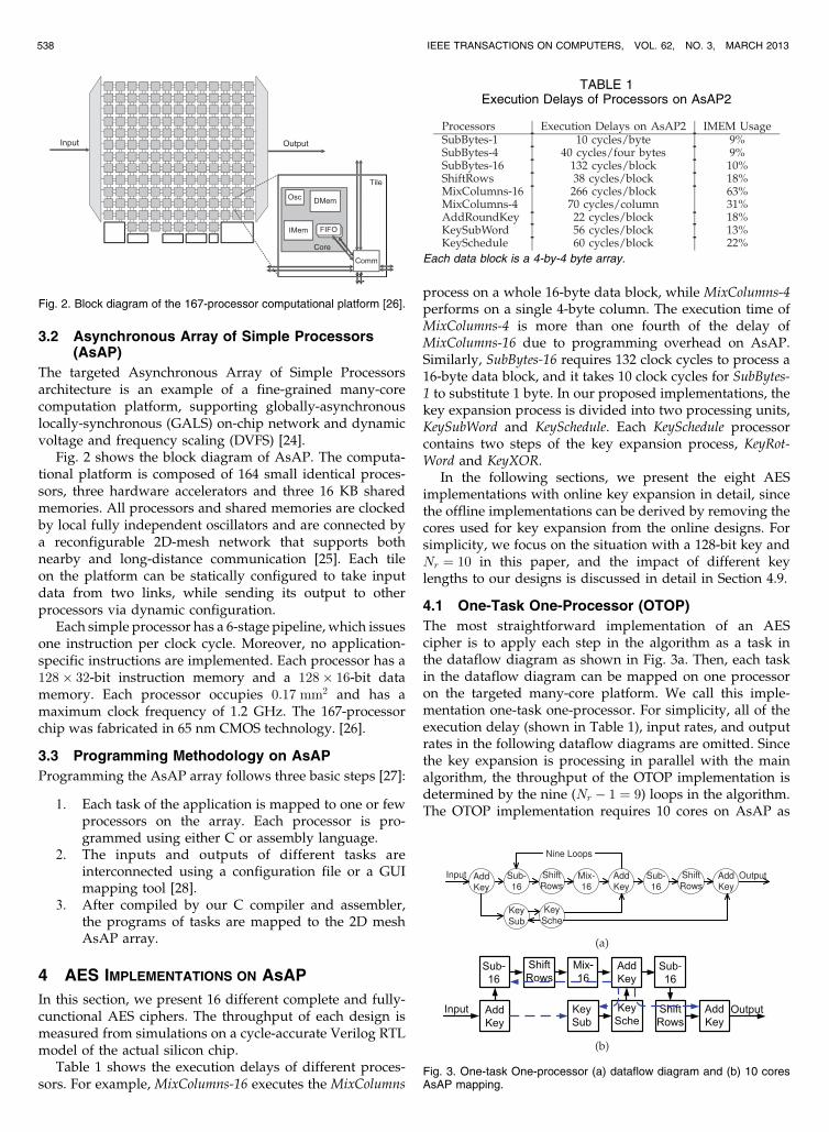
In this section, we present 16 different complete and fully-cunctional AES ciphers. The throughput of each design ismeasured from simulations on a cycle-accurate Verilog RTLmodel of the actual silicon chip.
Table 1 shows the execution delays of different proces-sors. For example, MixColumns-16 executes the MixColumns
process on a whole 16-byte data block, while MixColumns-4performs on a single 4-byte column. The execution time ofMixColumns-4 is more than one fourth of the delay ofMixColumns-16 due to programming overhead on AsAP.Similarly, SubBytes-16 requires 132 clock cycles to process a16-byte data block, and it takes 10 clock cycles for SubBytes-1 to substitute 1 byte. In our proposed implementations, thekey expansion process is divided into two processing units,KeySubWord and KeySchedule. Each KeySchedule processorcontains two steps of the key expansion process, KeyRot-Word and KeyXOR.
In the following sections, we present the eight AESimplementations with online key expansion in detail, sincethe offline implementations can be derived by removing thecores used for key expansion from the online designs. Forsimplicity, we focus on the situation with a 128-bit key andNr ¼ 10 in this paper, and the impact of different keylengths to our designs is discussed in detail in Section 4.9.
4.1 One-Task One-Processor (OTOP)
The most straightforward implementation of an AEScipher is to apply each step in the algorithm as a task inthe dataflow diagram as shown in Fig. 3a. Then, each taskin the dataflow diagram can be mapped on one processoron the targeted many-core platform. We call this imple-mentation one-task one-processor. For simplicity, all of theexecution delay (shown in Table 1), input rates, and outputrates in the following dataflow diagrams are omitted. Sincethe key expansion is processing in parallel with the mainalgorithm, the throughput of the OTOP implementation isdetermined by the nine (Nr � 1 ¼ 9) loops in the algorithm.The OTOP implementation requires 10 cores on AsAP as
538 IEEE TRANSACTIONS ON COMPUTERS, VOL. 62, NO. 3, MARCH 2013
Fig. 2. Block diagram of the 167-processor computational platform [26].
Fig. 3. One-task One-processor (a) dataflow diagram and (b) 10 coresAsAP mapping.
TABLE 1Execution Delays of Processors on AsAP2
Each data block is a 4-by-4 byte array.

shown in Fig. 3b. The throughput of the OTOP imple-mentation is 3,582 clock cycles per data block, equaling223.875 clock cycles per byte.
4.2 Loop-Unrolled Nine Times
To enhance the AES cipher’s throughput, we apply loopunrolling to the OTOP model and obtain the Loop-unrolledNine Times dataflow diagram as shown in Fig. 4a. The loopunrolling breaks the dependency among different loopsand allows the nine loops in the AES algorithm to operateon multiple data blocks simultaneously. To improve thethroughput as much as possible, we unroll the loops inboth the AES algorithm and the key expansion process byNr � 1 and Nr times, which equals 9 and 10, respectively.After loop unrolling, the throughput of the AES imple-mentation is increased to 266 cycles per data block,equaling 16.625 cycles per byte. The mapping of theLoop-unrolled Nine Times model is shown in Fig. 4b,which requires 60 cores.
4.3 Loop-Unrolled Three Times
To achieve a moderate throughput with fewer cores, wecould unroll the main loops in the AES algorithm byS times (S is divisible by Nr � 1), instead of Nr � 1 times.For this example, the nine loops in the AES algorithmcould be split into three blocks, and each block loops threetimes. The dataflow diagram and mapping of the Loop-unrolled Three Times implementation are shown inFigs. 5a and 5b, respectively. Compared to the OTOPmodel, the throughput is improved to 1,098 cycles per datablock, which equals 68.625 cycles per byte; while themapping requires 24 cores, 36 fewer than the Loop-unrolled Nine Times implementation.
4.4 Parallel-MixColumns
Besides loop unrolling, another way to increase thethroughput of the OTOP model is to reduce the main loop’slatency in the AES algorithm. In a single loop, the executiondelay of MixColumns-16 results in 60 percent of the totallatency. Each MixColumns-16 operates on a four-column datablock, and the operation on each column is independent.Therefore, each MixColumns-16 processor can be replaced by
four MixColumns-4s. Each MixColumns-4 actor computesonly one column rather than a whole data block. As a result,the throughput of the Parallel-MixColumns implementationis increased to 2,180 cycles per block, equaling 136.25 cyclesper byte. The dataflow diagram and mapping of the Parallel-MixColumns model are shown in Figs. 6a and 6b.
Each core on our targeted computational platform canonly support two statically configured input ports. Threecores, each called MergeCore, are used to merge the fourdata streams from MixColumns-4s into one stream forAddRoundKey.
LIU AND BAAS: PARALLEL AES ENCRYPTION ENGINES FOR MANY-CORE PROCESSOR ARRAYS 539
Fig. 4. Loop-unrolled Nine Times (a) dataflow diagram and (b) 60 coresAsAP mapping. Fig. 5. Loop-unrolled Three Times (a) dataflow diagram and (b) 24 cores
AsAP mapping.
Fig. 6. Parallel-MixColumns (a) dataflow diagram and (b) 16 cores AsAPmapping.

The dependence among bytes in one column diminishesthe performance improvement for further parallelization.For instance, if we parallelize one MixColumns-4 into twoMixColumns-2s, the effective execution delay of the MixCol-umns process is reduced to 64 cycles from 70 cycles. Thissaves only 6 cycles while it requires eight more processors(four extra MixColumns cores and four extra MergeCores).Therefore, further parallelization on the MixColumns processwould impair the area and energy efficiency of the entiresystem without significant performance improvement.
4.5 Parallel-SubBytes-MixColumns
In the Parallel-MixColumns implementation, SubBytes-16requires 132 cycles to encrypt one data block, whichcontributes the largest execution delay in one loop. In orderto increase the throughput further, we parallelize oneSubBytes-16 into four SubBytes-4s, which is shown in Fig. 7a.In this implementation, each SubBytes-4 processes 4 bytesrather than 16 bytes in one data block. The effectiveexecution delay of the SubBytes process is decreased to40 cycles per block, only around one fourth as before.Therefore, the throughput of the Parallel-SubBytes-MixCol-umns model is increased to 1,350 cycles per block, equaling84.375 cycles per byte. The mapping graph of the Parallel-SubBytes-MixColumns implementation on AsAP shown inFig. 7b requires 22 cores.
Instead of parallelizing SubBytes-16 into four SubByte-4s,we can replace it with 16 SubBytes-1s. The effective executiondelay of the SubBytes process is reduced to 10 cycles. As aresult, the latency of one-loop decreases to 120 cycles.Therefore, the throughput of the cipher is increased to
67.5 cycles per byte. However, it requires seven additionalcores dedicated to communication (four MergeCores andthree DispatchCores), which impair the area and energyefficiency of the implementation.
4.6 Full-Parallelism
The Full-parallelism AES implementation combines theParallel-SubBytes-MixColumns model and loop unrolling.The dataflow diagram and the mapping of the Full-parallelism model are shown in Figs. 8a and 8b. Asexpected, the throughput of this design is the highestamong all of the models introduced in this paper since itemploys most data and task parallelism. The throughput ofthe Full-parallelism model is 70 cycles per block, equaling4.375 cycles per byte. It also requires 164 cores, which is thelargest implementation of all.
In the Full-parallelism model, the MixColumns-4 proces-sors are the throughput bottlenecks which determine theperformance of the cipher. Therefore, parallelizing theSubBytes process with more than four processors wouldonly increase the area and power overhead without anyperformance improvement.
4.7 Small
The Small model implements an AES cipher on AsAP withthe fewest processors. As shown in Fig. 9, it requires at leasteight cores to implement an AES cipher with online keyexpansion process, since each core on AsAP has only a
128� 32-bit instruction memory and a 128� 16-bit datamemory. The throughput of the Small model is 2,678 cyclesper data block, which equals 167.375 cycles per byte.
540 IEEE TRANSACTIONS ON COMPUTERS, VOL. 62, NO. 3, MARCH 2013
Fig. 8. Full-parallelism (a) dataflow diagram and (b) 164 cores AsAPmapping.
Fig. 7. Parallel-SubBytes-MixColumns (a) dataflow diagram and(b) 22 cores AsAP mapping.

4.8 No-Merge-Parallelism
In contrast to the Small model, the No-merge-parallelismmodel exploits as much parallelism as possible withoutintroducing any cores dedicated to communication, includ-ing MergeCores and DispatchCores. The mapping graph of theNo-merge-parallelism implementation on AsAP is shown inFig. 10. To speed up the implementation, loop unrolling isapplied in this model. Each MixColumns-16 is divided intotwo MixColumns-8s, which helps reduce the effective delayof the MixColumns process. In order to eliminate additionalcommunication processors and simplify the routing, wecombine the SubBytes and the ShiftRows stages in one core.This implementation requires 59 cores, and has a through-put of 152 cycles per block, equaling 9.5 cycles per byte.
4.9 Designs with Longer Keys
As introduced in Section 2, besides the 128-bit key, the AESalgorithm also supports key lengths of 192 and 256 bits.Encrypting with longer keys results in two major areas ofadditional computation. First, the number of loops in theAES algorithm is increased. Second, the key expansioncores require more clock cycles to process round keys.
For the designs without loop-unrolling (Small, OTOP,Parallel-MixColumns, and Parallel-SubBytes-MixColumns),no extra cores are required. These mappings operate withlonger keys by increasing the number of round loops, Nr,and reprogramming the key expansion related cores. Thethroughputs of these designs are decreased due to theincreased number of Nr rounds.
For the designs with loop-unrolling, additional cores areadded depending on the number of rounds required. Forexample, 12 and 24 more cores are required for the No-merge-parallelism designs with a 192-bit and 256-bit key,respectively. The throughputs of the Loop-unrolled and theNo-merge-parallelism are kept the same as before, which isdetermined by the MixColumns operation. On the otherhand, for the Full-parallelism implementation, the through-put is decreased since the bottlenecks of the system areshifted from the MixColumn-4 processors to the key expan-sion cores, due to the overhead of processing longer keys.
Due to the significant effort required, 192-bit and 256-bitdesigns are not implemented in this work.
5 AREA EFFICIENCY ANALYSIS
Area is a significant metric in system design. Less areameans less silicon, therefore less cost. From a many-coreprocessor perspective, area is represented by the number ofcores required to implement applications. Smaller areatranslates into fewer used cores and leaves more opportu-nities for dealing with other applications on the sameplatform simultaneously. To evaluate the area efficiencybetween various AES implementations, a metric called
ThroughputPerCore is defined as the ratio between thethroughput of each design to the number of cores used toimplement it,
ThroughputPerCore ¼ Throughput
Number of Cores: ð2Þ
5.1 Area Optimization Methodology
Before comparing area efficiency among different AESimplementations, area optimization is applied to all of themodels without impairing performance. In this section, thearea optimization methodology is illustrated through adetailed example of minimizing the number of cores usedby the Full-parallelism model. As shown in Fig. 8b, there are17 cores in one loop of the Full-parallelism mapping,including five communication-dedicated cores, which areused for routing only. And the final round operation requires11 cores. Therefore, the number of cores utilized for theunoptimized Full-parallelism model is ðNr � 1Þ �None-loop þNlast-round ¼ 9� 17þ 11 ¼ 164.
Two optimization steps are applied to the Full-paralle-lism model. First, since the ShiftRows process is only byte-rotation, alternating the sequence of the SubBytes and theShiftRows stages would not affect encryption results. How-ever, this alternation reduces two MergeCores for each loop.As a result, 18 cores are reduced from the Full-parallelismmodel. Second, the throughput of the Full-parallelism modelis 70 cycles per block, which is determined by the operationdelay of MixColumns-4s. Any actors with less executiondelay would not impair the performance of the system.Therefore, a processor fusion of the ShiftRows in theNth loopand the AddRoundKey in the ðN � 1Þth loop can reduce onemore core for each loop, while keeping the same throughputsince these new combination processors take only 60 cyclesto process one data block. The dataflow diagram andmapping of the optimized Full-parallelism model are shownin Figs. 11a and 11b, respectively.
In summary, without losing any performance, thenumber of cores required by the online Full-parallelismmodel is decreased by approximately 16 percent to 137.
5.2 Area Efficiency Comparison
Based on the optimization methods discussed above, thenumber of cores utilized for each implementation isoptimized as follows:
1. Small: Optimization methods are not applicable.2. OTOP: The SubBytes and ShiftRows processors in the
last round are fused into one processor, saving oneprocessor.
LIU AND BAAS: PARALLEL AES ENCRYPTION ENGINES FOR MANY-CORE PROCESSOR ARRAYS 541
Fig. 10. Fifty Nine cores AsAP mapping of the No-merge-parallelismimplementation.
Fig. 9. Eight cores AsAP mapping of the Small implementation.

3. Parallel-MixColumns: The SubBytes and ShiftRowsprocessors in the last round are fused into oneprocessor, saving one processor.
4. Parallel-SubBytes-MixColumns: The sequence of theSubBytes and the ShiftRows stages is alternated,which saves three processors. The SubBytes andShiftRows processors in the last round are fused intoone processor, saving one more processor.
5. Loop-unrolled Three Times: The SubBytes andShiftRows processors in the last round are fused intoone processor, saving one processor.
6. Loop-unrolled Nine Times: The SubBytes and Shif-tRows processors in the same round are fused intoone processor, which saves 10 processors.
7. No-merge-parallelism: Optimization methods arenot applicable.
8. Full-parallelism: The optimization has been dis-cussed in detail in Section 5.1
5.2.1 Implementations with Online Key Expansion
The number of cores used for each optimized implementa-tion is shown in Column 3 of Table 2. As expected, theSmall implementation uses the fewest cores due to itssimplicity. On the other hand, the Full-parallelism modeloccupies 137 cores, exploiting the greatest range of types ofdata parallelism. As a result, the Full-parallelism imple-mentation requires 17� as many cores as the Small model,while it also gains a 40� throughput increase.
As defined in (2), ThroughputPerCore is used to comparethe area efficiency between different models. The higher thethroughput, the better the performance. The fewer the coresused, the smaller the area. As a result, a larger Throughput-PerCore ratio shows a higher area efficiency. In Table 2,Column 5 shows the ThroughputPerCore numbers of variousimplementations normalized to the Parallel-MixColumnsmodel with online key expansion. The No-merge-paralle-lism implementation has the highest throughput per corerate, since it avoids any dedicated communication cores andexploits as much parallelism as possible simultaneously.The Full-parallelism and the Loop-unrolled models alsooffer high throughput per unit of chip area. Although theSmall model has a relatively low throughput, it still offers agood area efficiency due to its extremely small area.
5.2.2 Implementations with Offline Key Expansion
Besides the online key expansion AES algorithm, thedetailed results of AES with offline key expansion are alsoshown in Columns 6, 7, and 8 of Table 2. The processorsused for key expansion process can be eliminated for theAES implementations with offline key expansion, whichresults in 29 percent improvement in average throughputper area compared to the implementations with onlinekey expansion.
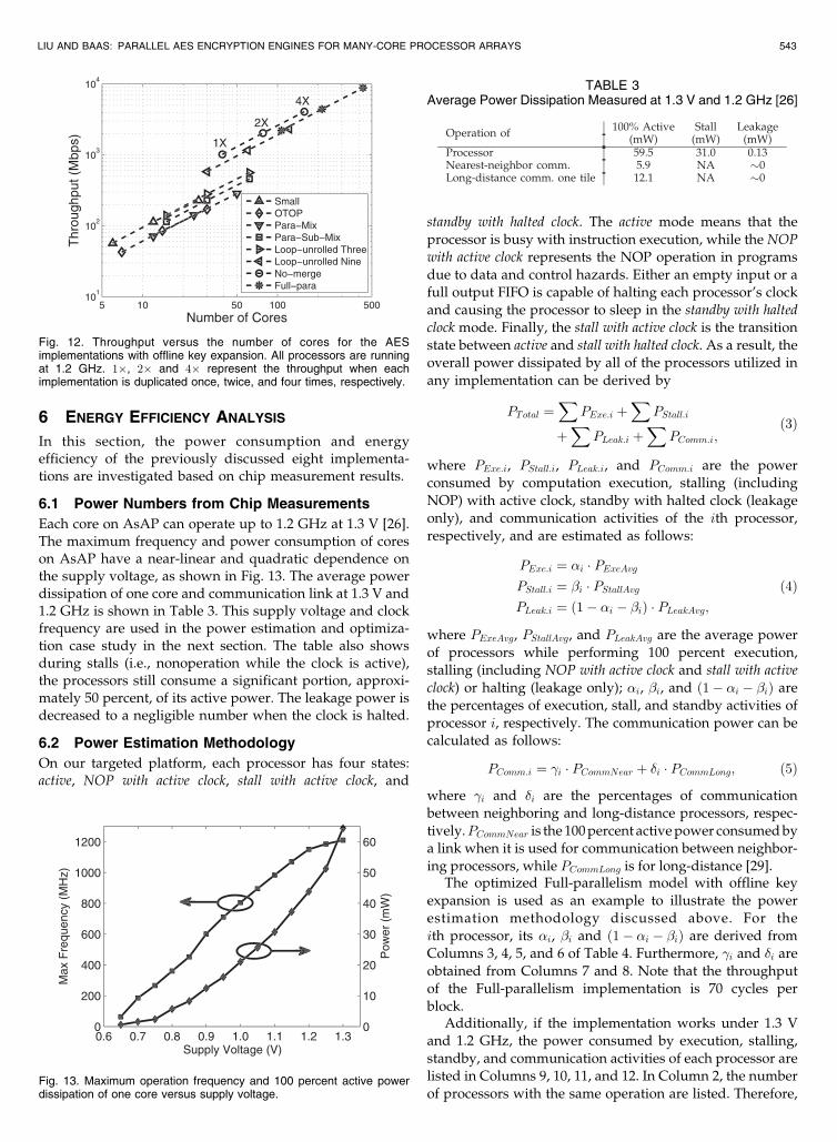
The throughput versus the number of cores of the eightoffline implementations is shown in Fig. 12. The through-put is obtained when all processors are running at 1.2 GHz.Besides the basic implementations discussed above, weduplicate each implementation two and four times to scalethe throughput and area. On the targeted platform, for anyscaled implementation with a 4� duplication, two merge-cores are required to gather the outputs for the subsequentprocessor by assuming each processor could take only twoinputs.
542 IEEE TRANSACTIONS ON COMPUTERS, VOL. 62, NO. 3, MARCH 2013
Fig. 11. Optimized Full-parallelism (a) dataflow diagram and (b) 137 coresAsAP mapping.
TABLE 2Throughput and the Number of Cores Required by Different Implementations
Communication cores are used for routing only, including MergeCores and DispatchCores. All of the throughput per core numbers are normalized tothe Parallel-Mixcolumns model with online key expansion.
6 ENERGY EFFICIENCY ANALYSIS
In this section, the power consumption and energyefficiency of the previously discussed eight implementa-tions are investigated based on chip measurement results.
6.1 Power Numbers from Chip Measurements
Each core on AsAP can operate up to 1.2 GHz at 1.3 V [26].The maximum frequency and power consumption of coreson AsAP have a near-linear and quadratic dependence onthe supply voltage, as shown in Fig. 13. The average powerdissipation of one core and communication link at 1.3 V and1.2 GHz is shown in Table 3. This supply voltage and clockfrequency are used in the power estimation and optimiza-tion case study in the next section. The table also showsduring stalls (i.e., nonoperation while the clock is active),the processors still consume a significant portion, approxi-mately 50 percent, of its active power. The leakage power isdecreased to a negligible number when the clock is halted.
6.2 Power Estimation Methodology
On our targeted platform, each processor has four states:active, NOP with active clock, stall with active clock, and
standby with halted clock. The active mode means that the
processor is busy with instruction execution, while the NOP
with active clock represents the NOP operation in programs
due to data and control hazards. Either an empty input or afull output FIFO is capable of halting each processor’s clock
and causing the processor to sleep in the standby with halted
clock mode. Finally, the stall with active clock is the transition
state between active and stall with halted clock. As a result, theoverall power dissipated by all of the processors utilized in
any implementation can be derived by
PTotal ¼X
PExe:i þX
PStall:i
þX
PLeak:i þX
PComm:i;ð3Þ
where PExe:i, PStall:i, PLeak:i, and PComm:i are the powerconsumed by computation execution, stalling (including
NOP) with active clock, standby with halted clock (leakageonly), and communication activities of the ith processor,
respectively, and are estimated as follows:
PExe:i ¼ �i � PExeAvgPStall:i ¼ �i � PStallAvgPLeak:i ¼ ð1� �i � �iÞ � PLeakAvg;
ð4Þ
where PExeAvg, PStallAvg, and PLeakAvg are the average power
of processors while performing 100 percent execution,stalling (including NOP with active clock and stall with active
clock) or halting (leakage only); �i, �i, and ð1� �i � �iÞ arethe percentages of execution, stall, and standby activities of
processor i, respectively. The communication power can becalculated as follows:
PComm:i ¼ �i � PCommNear þ �i � PCommLong; ð5Þ
where �i and �i are the percentages of communicationbetween neighboring and long-distance processors, respec-
tively.PCommNear is the 100 percent active power consumed bya link when it is used for communication between neighbor-
ing processors, while PCommLong is for long-distance [29].The optimized Full-parallelism model with offline key
expansion is used as an example to illustrate the powerestimation methodology discussed above. For the
ith processor, its �i, �i and ð1� �i � �iÞ are derived fromColumns 3, 4, 5, and 6 of Table 4. Furthermore, �i and �i are
obtained from Columns 7 and 8. Note that the throughputof the Full-parallelism implementation is 70 cycles per
block.Additionally, if the implementation works under 1.3 V
and 1.2 GHz, the power consumed by execution, stalling,
standby, and communication activities of each processor arelisted in Columns 9, 10, 11, and 12. In Column 2, the number
of processors with the same operation are listed. Therefore,
LIU AND BAAS: PARALLEL AES ENCRYPTION ENGINES FOR MANY-CORE PROCESSOR ARRAYS 543
Fig. 13. Maximum operation frequency and 100 percent active powerdissipation of one core versus supply voltage.
Fig. 12. Throughput versus the number of cores for the AESimplementations with offline key expansion. All processors are runningat 1.2 GHz. 1�, 2� and 4� represent the throughput when eachimplementation is duplicated once, twice, and four times, respectively.
TABLE 3Average Power Dissipation Measured at 1.3 V and 1.2 GHz [26]
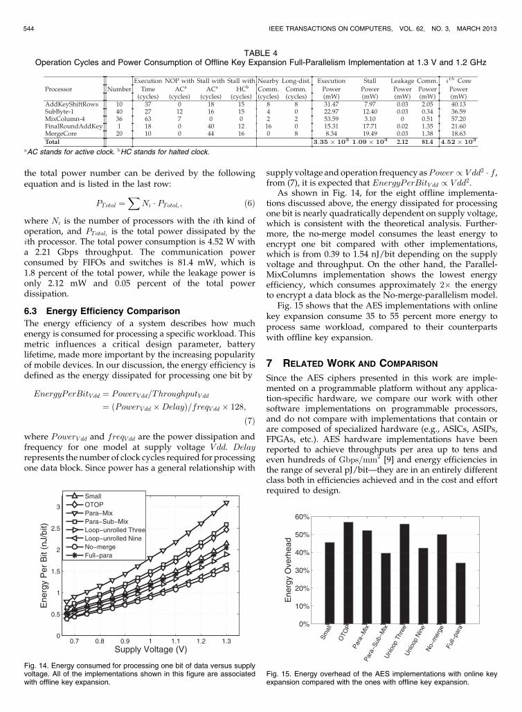
the total power number can be derived by the followingequation and is listed in the last row:
PTotal ¼X
Ni � PTotali ; ð6Þ
where Ni is the number of processors with the ith kind ofoperation, and PTotali is the total power dissipated by theith processor. The total power consumption is 4.52 W witha 2.21 Gbps throughput. The communication powerconsumed by FIFOs and switches is 81.4 mW, which is1.8 percent of the total power, while the leakage power isonly 2.12 mW and 0.05 percent of the total powerdissipation.
6.3 Energy Efficiency Comparison
The energy efficiency of a system describes how muchenergy is consumed for processing a specific workload. Thismetric influences a critical design parameter, batterylifetime, made more important by the increasing popularityof mobile devices. In our discussion, the energy efficiency isdefined as the energy dissipated for processing one bit by
EnergyPerBitV dd ¼ PowerV dd=ThroughputV dd¼ ðPowerV dd �DelayÞ=freqV dd � 128;
ð7Þ
where PowerV dd and freqV dd are the power dissipation andfrequency for one model at supply voltage V dd. Delayrepresents the number of clock cycles required for processingone data block. Since power has a general relationship with
supply voltage and operation frequency asPower / V dd2 � f ,from (7), it is expected that EnergyPerBitV dd / V dd2.
As shown in Fig. 14, for the eight offline implementa-tions discussed above, the energy dissipated for processingone bit is nearly quadratically dependent on supply voltage,which is consistent with the theoretical analysis. Further-more, the no-merge model consumes the least energy toencrypt one bit compared with other implementations,which is from 0.39 to 1.54 nJ/bit depending on the supplyvoltage and throughput. On the other hand, the Parallel-MixColumns implementation shows the lowest energyefficiency, which consumes approximately 2� the energyto encrypt a data block as the No-merge-parallelism model.
Fig. 15 shows that the AES implementations with onlinekey expansion consume 35 to 55 percent more energy toprocess same workload, compared to their counterpartswith offline key expansion.
7 RELATED WORK AND COMPARISON
Since the AES ciphers presented in this work are imple-mented on a programmable platform without any applica-tion-specific hardware, we compare our work with othersoftware implementations on programmable processors,and do not compare with implementations that contain orare composed of specialized hardware (e.g., ASICs, ASIPs,FPGAs, etc.). AES hardware implementations have beenreported to achieve throughputs per area up to tens andeven hundreds of Gbps=mm2 [9] and energy efficiencies inthe range of several pJ/bit—they are in an entirely differentclass both in efficiencies achieved and in the cost and effortrequired to design.
544 IEEE TRANSACTIONS ON COMPUTERS, VOL. 62, NO. 3, MARCH 2013
Fig. 14. Energy consumed for processing one bit of data versus supplyvoltage. All of the implementations shown in this figure are associatedwith offline key expansion.
TABLE 4Operation Cycles and Power Consumption of Offline Key Expansion Full-Parallelism Implementation at 1.3 V and 1.2 GHz
aAC stands for active clock. bHC stands for halted clock.
Fig. 15. Energy overhead of the AES implementations with online keyexpansion compared with the ones with offline key expansion.

A comprehensive comparison of the state-of-the-artsoftware AES implementations is summarized in Table 5.In order to make a fair comparison, all of the referenceddata are scaled to 65 nm CMOS technology with a supplyvoltage of 1.3 V. The area data are scaled to 65 nm with a1=ðs2Þ reduction, where s equals the ratio between theminimum feature size of the old technology and 65 nm. Thedelay and power data are scaled by SPICE simulationresults of a fanout-of-4 (FO4) inverter under differenttechnologies and supply voltages with predictive technol-ogy model (PTM) [31] as shown in Fig. 16.
As discussed in Section 5.2, we could always map one ofour designs for multiple times to get a higher throughputwhile possibly introducing a small overhead. Therefore, it isless meaningful to compare the throughput solely of eachdesign. In this section, we use the metrics of throughout perchip area (Gbps=mm2) and energy per workload bit (nJ/bit)to compare the area efficiency and energy efficiency ofvarious designs. As shown in Table 5, compared to the highlyoptimized AES ciphers on CPUs with bitslice [15], theproposed AES cipher on AsAP has 3.5-9.2 times higherthroughput per unit of chip area and consumes 9.5-11.3 timesless energy to encrypt a fixed amount of data. Besides bitslice,SIMD instructions are applied to improve the throughputand efficiency of AES implementations on CPUs further [19].Even so, our design on AsAP still has 10.7-15.6 times higherthroughput per unit of chip area and 8.2-18.1 times lowerenergy per bit. The TI DSP C6201 is an 8-way VLIWarchitecture for high performance DSP applications. Thereferenced data shows that our design has 2 times higherthroughput. The area and power numbers of the TI DSPC6201 are not available, but we believe that AsAP hassignificantly higher throughput per unit of chip area andenergy efficiency due to a much smaller core size.
The AES implementation on GeForce 8,800 GTX achievesthe highest throughput in the referenced designs, due to its
LIU AND BAAS: PARALLEL AES ENCRYPTION ENGINES FOR MANY-CORE PROCESSOR ARRAYS 545
TABLE 5Comparison of AES Cipher Implementations on Different Software Platforms
The original data are presented with different CMOS technologies and supply voltages. For comparison, area, performance, and power consumptionare scaled to 65 nm technology with a supply voltage of 1.3 V. Area are scaled by 1=ðs2Þ. Throughput and power numbers are scaled based on thePTM simulation results shown in Fig. 16. aThe typical power is not available, so 50 percent of thermal design power (TDP) is used based on thebenchmark data of a general-purpose processor [30]. bThe throughput results from [19] are for only one core, so the area and power numbers arescaled proportionally. cAll referenced designs do not consider key expansion; therefore, the AES implementations on AsAP associated with offlinekey expansion are applied for a fair comparison.
Fig. 16. Delay and power of a FO4 inverter based on SPICE simulationusing predictive technology model [32]; the general scaling rule assumesa 1=s reduction in delay and a 1=ðv2Þ reduction in power where s is thetechnology scaling factor and v is the voltage scaling factor [33].

large chip area and the utilization of the T-Box method,which works effectively for SIMD architectures with largememory [22]. However, our design still shows a 3.3 timeshigher throughput per unit of chip area and 2.9 times higherenergy efficiency.
Fig. 17 shows that the software AES implementation onAsAP outperforms other software platforms in terms ofenergy efficiency and performance per area.
8 CONCLUSION
We have presented 16 different AES cipher implementa-tions with both online and offline key expansion on afine-grained many-core system. Each implementationexploits different levels of data and task parallelism. Thesmallest design requires only six processors, equaling1:02 mm2 in a 65 nm fine-grained many-core system. Thefastest design achieves a throughput of 4.375 cycles perbyte, which is 2.21 Gbps when the processors are runningat a frequency of 1.2 GHz. We also optimize the area ofeach implementation by examining the workload of eachprocessor, which reduces the number of cores used asmuch as 18 percent. The design on the fine-grained many-core system achieves energy efficiencies approximately2.9-18.1 times higher than other software platforms, andperformance per area on the order of 3.3-15.6 timeshigher. Overall, the fine-grained many-core system hasbeen demonstrated to be a very promising platform forsoftware AES implementations.
ACKNOWLEDGMENTS
The authors gratefully acknowledge support from USNational Science Foundation (NSF) Grants 0430090,0903549 and CAREER Award 0546907, SRC GRC Grants1598 and 1971, CSR Grant 1659, UC Micro, ST Microelec-tronics, Center of Circuit and System Solutions (C2S2), Intel,and Intellasys. The authors also acknowledge the support ofthe C2S2 Focus Center, one of six research centers fundedunder the Focus Center Research Program (FCRP), aSemiconductor Research Corporation entity.
REFERENCES
[1] NIST, “Advanced Encryption Standard (AES),” http://csrc.nist.-gov/publications/fips/fips197/fips-197.pdf, Nov. 2001.
[2] NIST, “Data Encryption Standard (DES),” http://csrc.nist.gov/publications/fips/fips46-3/fips46-3.pdf, Oct. 1999.
[3] I. Verbauwhede, P. Schaumont, and H. Kuo, “Design andPerformance Testing of a 2.29 gb/s Rijndael Processor,” IEEEJ. Solid-State Circuits, vol. 38, no. 3, pp. 569-572, Mar. 2003.
[4] D. Mukhopadhyay and D. RoyChowdhury, “An Efficient end toEnd Design of Rijndael Cryptosystem in 0:18�m CMOS,” Proc.18th Int’l Conf. VLSI Design, pp. 405-410, Jan. 2005.
[5] J.L. Hennessy and D.A. Patterson, Computer Architecture: AQuantitative Approach, fourth ed. Morgan Kaufmann, 2007.
[6] S. Morioka and A. Satoh, “A 10-gbps full-AES Crypto Design witha Twisted BDD s-Box Architecture,” IEEE Trans. Very Large ScaleIntegration Systems, vol. 12, no. 7, pp. 686-691, July 2004.
[7] J. Daemen and V. Rijmen, The Design of Rijndael. Springer-Verlag,2002.
[8] A. Hodjat and I. Verbauwhede, “Area-Throughput Trade-Offs forFully Pipelined 30 to 70 Gbits/s AES Processors,” IEEE Trans.Computers, vol. 55, no. 4, pp. 366-372, Apr. 2006.
[9] S.K. Mathew, F. Sheikh, M. Kounavis, S. Gueron, A. Agarwal, S.K.Hsu, H. Kaul, M.A. Anders, and R.K. Krishnamurthy, “53 gbpsNative GF(ð24Þ2) Composite-Field AES-Encrypt/Decrypt Accel-erator for Content-Protection in 45 nm High-Performance Micro-processors,” IEEE J. Solid-State Circuits, vol. 46, no. 4, pp. 767-776,Apr. 2011.
[10] A. Hodjat and I. Verbauwhede, “A 21.54 gbits/s FullyPipelined AES Processor on FPGA,” Proc. IEEE 12th Ann.Symp. Field-Programmable Custom Computing Machines, pp. 308-309, Apr. 2004.
[11] C.-J. Chang, C.-W. Huang, K.-H. Chang, Y.-C. Chen, and C.-C.Hsieh, “High Throughput 32-Bit AES Implementation in FPGA,”Proc. IEEE Asia Pacific Conf. Circuits and Systems, pp. 1806-1809,Nov. 2008.
[12] J. Granado-Criado, M. Vega-Rodriguez, J. Sanchez-Perez, and J.Gomez-Pulido, “A New Methodology to Implement the AESAlgorithm Using Partial and Dynamic Reconfiguration,” Integra-tion, the VLSI J., vol. 43, no. 1, pp. 72-80, 2010.
[13] S. Qu, G. Shou, Y. Hu, Z. Guo, and Z. Qian, “HighThroughput, Pipelined Implementation of AES on FPGA,” Proc.Int’l Symp. Information Eng. and Electronic Commerce, pp. 542-545,May 2009.
[14] “Int’l Technology Roadmap for Semiconductors, Design,” http://www.itrs.net/Links/2009ITRS/2009Chapters_2009Tables/2009_Design.pdf, 2009.
[15] M. Matsui and J. Nakajima, “On the Power of Bitslice Implemen-tation on Intel Core 2 Processor,” Proc. Cryptographic Hardware andEmbedded Systems (CHES ’07), pp. 121-134, 2007.
[16] E. Biham, “A Fast New DES Implementation in Software,”Proc. Fourth Int’l Workshop Fast Software Encryption, pp. 260-272,1997.
[17] D. Bernstein and P. Schwabe, “New AES Software SpeedRecords,” Proc. INDOCRYPT ’08: Ninth Int’l Conf. Cryptology inIndia: Progress in Cryptology, pp. 322-336, 2008.
[18] “Supplemental Streaming SIMD Extensions 3,” http://en.ikipedia.org/wiki/SSSE3, 2012.
[19] E. Kasper and P. Schwabe, “Faster and Timing-Attack ResistantAES-GCM,” Proc. 11th Int’l Workshop Cryptographic Hardware andEmbedded Systems (CHES ’09), pp. 1-17, 2009.
[20] S. Gueron, “Intel Advanced Encryption Standard (AES) Instruc-tions Set,” Jan. 2010.
[21] T. Wollinger, M. Wang, J. Cuajardo, and C. Paar, “How Well areHigh-end DSPs Suited for the AES Algorithm?,” Proc. Third AESCandidate Conf., pp. 94-105, Apr. 2000.
[22] S.A. Manavski, “CUDA Compatible GPU as an Efficient Hard-ware Accelerator for AES Cryptography,” Proc. IEEE Int’l Conf.Signal Processing and Comm., pp. 65-68, Nov. 2007.
[23] S. Borkar, “Thousand Core Chips: A Technology Perspective,”Proc. 44th Ann. Design Automation Conf., pp. 746-749, 2007.
[24] D. Truong, W. Cheng, T. Mohsenin, Z. Yu, T. Jacobson, G. Landge,M. Meeuwsen, C. Watnik, P. Mejia, A. Tran, J. Webb, E. Work, Z.Xiao, and B. Baas, “A 167-Processor 65 nm ComputationalPlatform with Per-Processor Dynamic Supply Voltage andDynamic Clock Frequency Scaling,” Proc. IEEE Symp. VLSICircuits, June 2008.
546 IEEE TRANSACTIONS ON COMPUTERS, VOL. 62, NO. 3, MARCH 2013
Fig. 17. Comparison of peak performance per area and workload perunit energy of programmable processors. All numbers are scaled basedon the PTM simulation results shown in Fig. 16.

[25] A.T. Tran, D.N. Truong, and B.M. Baas, “A ReconfigurableSource-Synchronous On-Chip Network for GALS Many-CorePlatforms,” IEEE Trans. Computer-Aided Design of IntegratedCircuits and Systems, vol. 29, no. 6, pp. 897-910, June 2010.
[26] D.N. Truong, W.H. Cheng, T. Mohsenin, Z. Yu, A.T. Jacobson, G.Landge, M.J. Meeuwsen, A.T. Tran, Z. Xiao, E.W. Work, J.W.Webb, P. Mejia, and B.M. Baas, “A 167-Processor ComputationalPlatform in 65 nm CMOS,” IEEE J. Solid-State Circuits, vol. 44, no. 4,pp. 1130-1144, Apr. 2009.
[27] B. Baas, Z. Yu, M. Meeuwsen, O. Sattari, R. Apperson, E. Work, J.Webb, M. Lai, T. Mohsenin, D. Truong, and J. Cheung, “AsAP:A Fine-Grained Many-Core Platform for DSP Applications,” IEEEMicro, vol. 27, no. 2, pp. 34-45, Mar. 2007.
[28] E.W. Work, “Algorithms and Software Tools for MappingArbitrarily Connected Tasks onto an Asynchronous Array ofSimple Processors,” MS thesis, Univ. of California, Davis, Sept.2007.
[29] Z. Yu and B.M. Baas, “A Low-Area Multi-Link InterconnectArchitecture for GALS Chip Multiprocessors,” IEEE Trans. VeryLarge Scale Integration (VLSI) Systems, vol. 18, no. 5, pp. 750-762,May 2010.
[30] M. Butler, “AMD Bulldozer Core—A New Approach to Multi-threaded Compute Performance for Maximum Efficiency andThroughput,” Proc. IEEE HotChips Symp. High-Performance Chips(HotChips ’10), Aug. 2010.
[31] A. Stillmaker, “Exploration of Technology Scaling of CMOSCircuits from 180 nm to 22 nm Using PTM Models in HSPICE,”technical report, UC Davis, June 2011.
[32] W. Zhao and Y. Cao, “New Generation of Predictive TechnologyModel for Sub-45 nm Early Design Exploration,” IEEE Trans.Electron Devices, vol. 53, no. 11, pp. 2816-2823, Nov. 2006.
[33] J.M. Rabaey, A. Chandrakasan, and B. Nikolic, Digital IntegratedCircuits: A Design Perspective, second ed. Prentice-Hall, 2003.
Bin Liu received the BS degree in informationengineering from Shanghai Jiao Tong Univer-sity, China, in 2007, and the MS degree inelectrical and computer engineering from theUniversity of California, Davis, in 2010, where heis currently toward the PhD degree. His researchinterests include high-performance multicoreprocessor architecture, variation-aware dynamicand frequency scaling algorithms and circuits,and parallel encryption engine implementations.
He received the Best Paper nomination at Asilomar 2011. He is astudent member of the IEEE.
Bevan M. Baas received the BS degree inelectronic engineering from California Polytech-nic State University, San Luis Obispo, in 1987,and the MS and PhD degrees in electricalengineering from Stanford University, CA, in1990 and 1999, respectively. From 1987 to1989, he was with Hewlett-Packard, Cupertino,CA, where he participated in the development ofthe processor for a high-end minicomputer. In1999, he joined Atheros Communications, Santa
Clara, CA, as an early employee and served as a core member of theteam which developed the first IEEE 802.11a (54 Mbps, 5 GHz) Wi-Fiwireless LAN solution. In 2003 he joined the Department of Electricaland Computer Engineering at the University of California, Davis, wherehe is now an associate professor. He leads projects in architecture,hardware, software tools, and applications for VLSI computation with anemphasis on DSP workloads. Recent projects include the 36-processorAsynchronous Array of simple Processors (AsAP) chip, applications,and tools; a second generation 167-processor chip; low density paritycheck (LDPC) decoders; FFT processors; viterbi decoders; and H.264video codecs. Dr. Baas was a US National Science Foundation fellowfrom 1990 to 1993 and a NASA Graduate Student Researcher fellowfrom 1993 to 1996. He was a recipient of the US National ScienceFoundation CAREER Award in 2006 and the Most Promising Engineer/Scientist Award by AISES in 2006. He received the Best Paper Award atICCD 2011, and Best Paper nominations at Asilomar 2011 and BioCAS2010. During the summer of 2006 he was a visiting professor in Intel’sCircuit Research Lab. He is an associate editor for the IEEE Journal ofSolid-State Circuits and IEEE Micro guest editor in 2012. He has beenthe program committee cochair of HotChips in 2011, and programcommittee member of Hotchips in 2009-2010, of ICCD in 2004–2005and 2007–2009, of ASYNC in 2010, and of the ISSCC SRP Forum in2012. He is a senior member of the IEEE.
. For more information on this or any other computing topic,please visit our Digital Library at www.computer.org/publications/dlib.
LIU AND BAAS: PARALLEL AES ENCRYPTION ENGINES FOR MANY-CORE PROCESSOR ARRAYS 547


![Der Advanced Encryption Standard [AES]Der Advanced Encryption Standard [AES] Autoren: Christof Paar Jan Pelzl Ruhr - Universität Bochum Der Advanced Encryption Stan-dard [AES] Autoren:](https://img.pdfslide.us/doc/110x75/5f94f8f21b26e621c24ffacc/der-advanced-encryption-standard-aes-der-advanced-encryption-standard-aes-autoren.jpg)