Embed Size (px)
Citation preview
A Background Calibration Method for DAC Mismatch Correction in Multibit Sigma-Delta Modulators
Shafqat Ali, Steve Tanner and Pierre Andre FarineSwiss Federal Institute of Technology (EPFL), 1015 Lausanne, Switzerland.
[email protected], [email protected]
Abstract—A topology for the calibration of DAC errors in multi-bit sigma delta modulators is presented. The proposed technique enables the calibration to proceed in the background. In this technique, two DACs are used in a time-interleaved fashion. One DAC is calibrated at a time while the other is connected to the modulator. The technique is demonstrated by a design in UMC 0.18 µm CMOS technology which shows a very competitive figure of merit of 78fJ/Conv-Step. The extensive simulation results are presented to validate the results.
Keywords: DAC, calibration, background, ADC, sigma-delta, modulator.
I. INTRODUCTION Sigma delta modulators (SDM) are an important type of data converter. Their robustness to the non-idealities of analog circuits is their main advantage [1]. Therefore, the feature size reduction in CMOS process, which complicates analog circuit design [2], makes these SDMs more attractive. The two main types of SDMs are continuous time and discrete time. For each of them, the feedback DAC can be single or multi-bit type. The main advantage of using 1 bit feedback DAC is the inherent linearity of it. However, a multi-bit DAC is an attractive alternative for many reasons. SDMs using multi-bit DACs have relaxed stability requirements, their coefficients can be aggressively scaled to achieve more dynamic range, the amplifiers have reduced swing requirements, and they show higher SQNR (signal to quantization noise ratio) for a given oversampling ratio [3]. However, the major difficulty of multi-bit SDMs is the DAC non-linearity. Since the feedback DAC provides its output directly to the input of the modulator, its linearity directly affects the linearity of SDM.
In this paper, we present a simple method for linearization of the feedback DAC through digital calibration. This technique is somewhat similar to [4] and [5]. Contrary to [4-5] the proposed calibration method is performed in the background (online), while the modulator is operating. Therefore, it does not disrupt the regular operation. The proposed method uses two DACs (each consists of a binary weighted capacitors bank). When one DAC is used with the modulator, the other is calibrated with a high-resolution (at least equal to the desired resolution from the SDM) calibrating ADC. This speed of the calibrating ADC is not critical.
In section I, we discuss the top level structure of the SDM and the calibration scheme. This is followed by section II where we discuss the specifications and design of the SDM
building blocks. In section III, simulation results are given, followed by a conclusion.
II. BLOCK LEVEL ARCHITECTURE OF SDMIn this paper, we present a 3rd-order sigma delta modulator
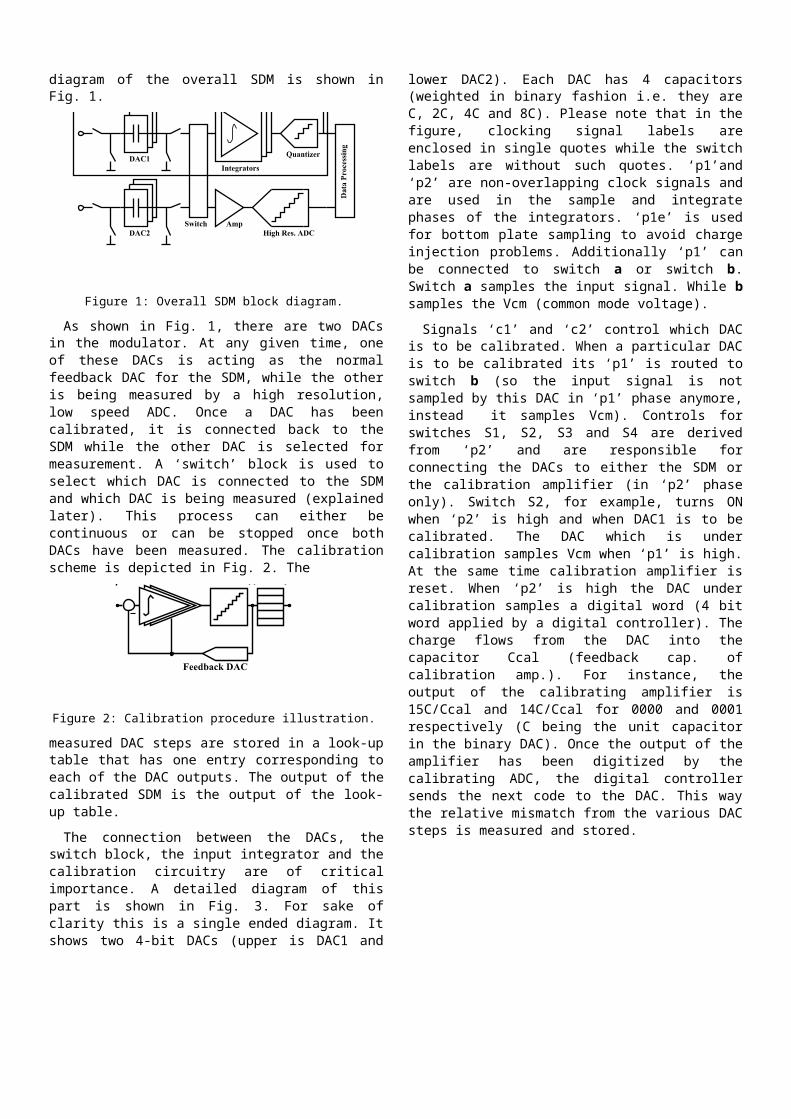
with 4 bit feedback DAC, as a proof of concept. The block diagram of the overall SDM is shown in Fig. 1.
Figure 1: Overall SDM block diagram.
As shown in Fig. 1, there are two DACs in the modulator. At any given time, one of these DACs is acting as the normal feedback DAC for the SDM, while the other is being measured by a high resolution, low speed ADC. Once a DAC has been calibrated, it is connected back to the SDM while the other DAC is selected for measurement. A ‘switch’ block is used to select which DAC is connected to the SDM and which DAC is being measured (explained later). This process can either be continuous or can be stopped once both DACs have been measured. The calibration scheme is depicted in Fig. 2. The
Figure 2: Calibration procedure illustration.
measured DAC steps are stored in a look-up table that has one entry corresponding to each of the DAC outputs. The output of the calibrated SDM is the output of the look-up table.
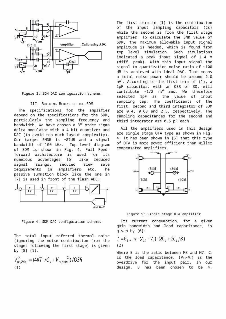
The connection between the DACs, the switch block, the input integrator and the calibration circuitry are of critical importance. A detailed diagram of this part is shown in Fig. 3. For sake of clarity this is a single ended diagram. It shows two 4-bit DACs (upper is DAC1 and lower DAC2). Each DAC has 4 capacitors (weighted in binary fashion i.e. they are C, 2C, 4C and 8C). Please note that in the figure, clocking signal labels are enclosed in single quotes while the switch labels are without such quotes. ‘p1’and ‘p2’ are non-overlapping clock signals and are used in the sample and integrate phases of the integrators. ‘p1e’ is used for bottom plate sampling to avoid charge injection problems. Additionally ‘p1’ can be connected to switch a or switch b. Switch a samples the input signal. While b samples the Vcm (common mode voltage).
Signals ‘c1’ and ‘c2’ control which DAC is to be calibrated. When a particular DAC is to be calibrated its ‘p1’ is routed to switch b (so the input signal is not sampled by this DAC in ‘p1’ phase anymore, instead it samples Vcm). Controls for switches S1, S2, S3 and S4 are derived from ‘p2’ and are responsible for connecting the DACs to either the SDM or the calibration amplifier (in ‘p2’ phase only). Switch S2, for example, turns ON when ‘p2’ is high and when DAC1 is to be calibrated. The DAC which is under calibration samples Vcm when ‘p1’ is high. At the same time calibration amplifier is reset. When ‘p2’ is high the DAC under calibration samples a digital word (4 bit word applied by a digital controller). The charge flows from the DAC into the capacitor Ccal (feedback cap. of calibration amp.). For instance, the output of the calibrating amplifier is 15C/Ccal and 14C/Ccal for 0000 and 0001 respectively (C being the unit capacitor in the binary DAC). Once the output of the amplifier has been digitized by the calibrating ADC, the digital controller sends the next code to the DAC. This way the relative mismatch from the various DAC steps is measured and stored.
Figure 3: SDM DAC configuration scheme.
III. BUILDING BLOCKS OF THE SDMThe specifications for the amplifier depend on the
specifications for the SDM, particularly the sampling frequency and bandwidth. We have chosen a 3rd order sigma delta modulator with a 4 bit quantizer and DAC (to avoid too
much layout complexity). Our target SNDR is ~87dB and a signal bandwidth of 100 kHz. Top level diagram of SDM is shown in Fig. 4. Full Feed-forward architecture is used for its numerous advantages [6] like reduced signal swings, reduced slew rate requirements in amplifiers etc. The passive summation block like the one in [7] is used in front of the flash ADC.
Figure 4: SDM DAC configuration scheme.
The total input referred thermal noise (ignoring the noise contribution from the stages following the first stage) is given by [8] (1).
(1)
The first term in (1) is the contribution of the input sampling capacitors (Cs) while the second is from the first stage amplifier. To calculate the SNR value of SDM, the maximum allowable input signal amplitude is needed, which is found from top level simulation. Such simulations indicated a peak input signal of 1.4 V (diff. peak). With this input signal the signal to quantization noise ratio of ~100 dB is achieved with ideal DAC. That means a total noise power should be around 2.0 nV2. According to the first term of (1), a 1pF capacitor, with an OSR of 30, will contribute ~1/2 nV2 rms. We therefore selected 1pF as the value of input sampling cap. The coefficients of the first, second and third integrator of SDM are 0.4, 0.68 and 2.5, respectively. The sampling capacitances for the second and third integrator are 0.5 pF each.
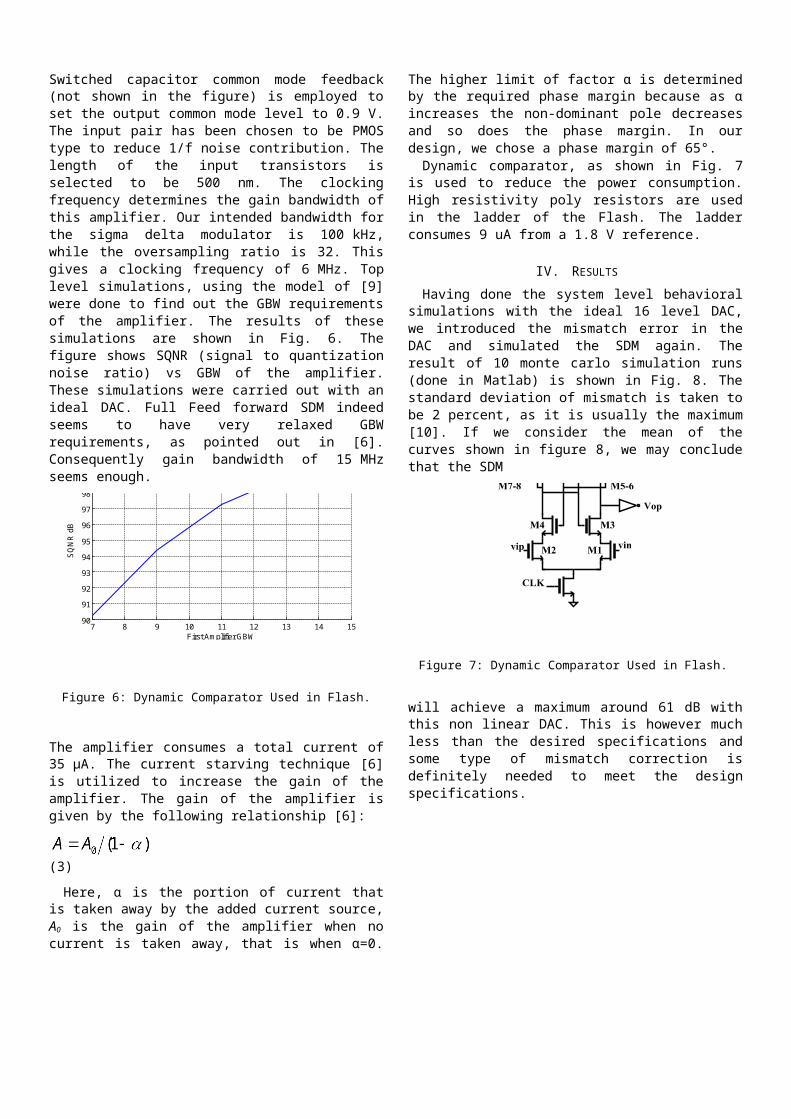
All the amplifiers used in this design are single stage OTA type as shown in Fig. 4. It has been shown in [6] that this type of OTA is more power efficient than Miller compensated amplifiers.
Figure 5: Single stage OTA amplifier
Its current consumption, for a given gain bandwidth and load capacitance, is given by [6]:
(2)
Where B is the ratio between M8 and M7. CL is the load capacitance. (VGS-Vt) is the overdrive for the input pair. In our design, B has been chosen to be 4. Switched capacitor common mode feedback (not shown in the figure) is employed to set the output common mode level to 0.9 V. The input pair has been chosen to be PMOS type to reduce 1/f noise contribution. The length of the input transistors is selected to be 500 nm. The clocking frequency determines the gain bandwidth of this amplifier. Our intended bandwidth for the sigma delta modulator is 100 kHz, while the oversampling ratio is 32. This gives a clocking frequency of 6 MHz. Top level simulations, using the model of [9] were done to find out the GBW requirements of the amplifier. The results of these simulations are shown in Fig. 6. The figure shows SQNR (signal to quantization noise ratio) vs GBW of the amplifier. These simulations were carried out with an ideal DAC. Full Feed forward SDM indeed seems to have very relaxed GBW requirements, as pointed out in [6]. Consequently gain bandwidth of 15 MHz seems enough.
7 8 9 10 11 12 13 14 1590
91
92
93
94
95
96
97
98
99
100
First Amplifier GBW
SQ
NR
dB
SQNR (with ideal DAC) Vs GBW of First Amplifier
Figure 6: Dynamic Comparator Used in Flash.
The amplifier consumes a total current of 35 µA. The current starving technique [6] is utilized to increase the gain of the amplifier. The gain of the amplifier is given by the following relationship [6]:
(3)
Here, α is the portion of current that is taken away by the added current source, A0 is the gain of the amplifier when no current is taken away, that is when α=0. The higher limit of factor α is determined by the required phase margin because as α increases the non-dominant pole decreases and so does the phase margin. In our design, we chose a phase margin of 65°.
Dynamic comparator, as shown in Fig. 7 is used to reduce the power consumption. High resistivity poly resistors are used in the ladder of the Flash. The ladder consumes 9 uA from a 1.8 V reference.
IV. RESULTS
Having done the system level behavioral simulations with the ideal 16 level DAC, we introduced the mismatch error in the DAC and simulated the SDM again. The result of 10 monte carlo simulation runs (done in Matlab) is shown in Fig. 8. The standard deviation of mismatch is taken to be 2 percent, as it is usually the maximum [10]. If we consider the mean of the curves shown in figure 8, we may conclude that the SDM
Figure 7: Dynamic Comparator Used in Flash.
will achieve a maximum around 61 dB with this non linear DAC. This is however much less than the desired specifications and some type of mismatch correction is definitely needed to meet the design specifications.
-70 -60 -50 -40 -30 -20 -10-10
0
10
20
30
40
50
60
70
Input Amplitude, Normalized to Vref
SN
DR
dB
SDM Performance With Non Ideal DAC
Figure 8: Monte Carlo Simulations With DAC Mismatch
In Fig. 9 we show the results of SNDR simulations with and without the proposed calibration scheme. For this simulation 131072 points simulations were done in cadence. The results are imported into MATLAB for analysis. The lower (green) curve is the result of simulation without the calibration while the upper (blue) is the one with calibration. The SDM consumes 158 µA (105 µA for amplifiers, 13 µA in Flash and 40µA in digital circuitry) and achieves a peak SNDR of 87.8 dB. The calibration ADC is an incremental type ADC and uses 150 µA. The power consumed by the calibration circuit is not critical because this circuit is turned OFF when the calibration is complete. The fJ/Conv-Step FOM would be then given by (4).
= 77.3 fJ/Conv (4)
-90 -80 -70 -60 -50 -40 -30 -20 -10-20
0
20
40
60
80
100
Input Amplitude, Normalized to Vref
SN
DR
dB
SNDR With And Without Calibration
Figure 9: Monte Carlo Simulations With DAC Mismatch
A comparison with the state of the art is listed in the Table I.
Table I: Comparison with the other published work
Work Technology BW FOM fJ/Conv-Step
This Work 0.18µm 100 kHz 77.3[11] 32nm 20 MHz 606[12] 40nm 1.92 MHz 112[13] 0.18µm 100 KHz 108[14] 90nm 25MHz 87.7[15] 90nm 25MHz 130
Please note that we did not include the power of calibration circuit in the calculation of FOM. If we run the calibration circuit 1 percent of the time (out of every 100 time units of circuit operation calibration runs for 1 unit of time) then the FOM would degrade to 78 fJ/Conv-Step from 77.3 fJ/conv-step.Table II summarizes the main parameters and performances of the overall SDM.
Table II: Summary of obtained SDM performance.
Technology 0.18µmPower Supply 1.8V
Current Consumption 158 µASNDR 87dB
Signal Bandwidth 100 kHzSampling Frequency 6 MHz
FOM 77.3 fJ/Conv
V. CONCLUSION
In this paper, we present a DAC calibration technique for multibit Sigma-Delta modulators. The method is based on the duplication of the DAC: the first one is calibrated while the other is used in the SDM. The drawback of this approach is the use of an extra calibrating ADC for the feedback DAC. The power of this extra ADC is however not a big concern as it can be turned off once the calibration has been done. Simulation results show that very competitive figure of merit,
hence higher power efficiency, can be achieved with this calibration approach.
ACKNOWLEDGEMENTS
This work was funded by the NanoTera program of Swiss National Science Foundation (SNF) under Grant No. 6309903. The Swiss National Science Foundation is thankfully acknowledged.
REFERENCES
[1] José M. de la Rosa, “Sigma-Delta Modulators: Tutorial Overview, Design Guide and State-of-the-Art Survey”, IEEE Transactions on Circuits and Systems—I: Regular Papers, Vol. 58, No. 1,January 2011.
[2] A. Annema, B Nauta, R Langevelde, H Tuinhout, “Analog Circuits in Ultra-Deep-Submicron CMOS”, IEEE JSSC, Vol. 40, No. 1, January 2005.
[3] Anas A. Hamoui and Kenneth W. Martin, “High-Order Multibit Modulators and Pseudo Data-Weighted-Averaging in Low-Oversampling”, IEEE Transactions on Circuits and Systems—I: Rregular Papers, Vol. 51, No. 1,January 2004.
[4] Mohammad Sarhang-Nejad and Gabor C. Temes, “A High-Resolution Multibit EA ADC with Digital Correction and Relaxed Amplifier Requirements”, IEEE Journal of Solid-State Circuits, Vol. 28, No. 6, june 1993.
[5] Kentaro Yamamoto, Anthony Chan Carusone and Francis P. Dawson, “A Delta-Sigma Modulator With a Widely Programmable Center Frequency and 82-dB Peak SNDR”, IEEE Journal of Solid-State Circuits, Vol. 43, No. 8, August 2008.
[6] L. Yao, M. Steyaert and W. Sansen, "Low-Power Low-Voltage Sigma-Delta Modulators in Nanometer CMOS", Springer, the Netherlands, ISBN: 1-4020-4139-X.
[7] Ki Y.N, Su D.K, Vleugels K, Wooley B.A, “A 0.7-V 100-dB 870-μW digital audio ΣΔ modulator”, IEEE Journal of Solid-State Circuits, Vol. 44, No. 4, pp. 1078-1088, May 2009.
[8] Course notes from “Practical Aspects in Mixed Signal Design” http://www.mead.ch.
[9] S.Brigati,F. Francesconi, P. Malcovati, D. Tonietto, A. Baschirotto and F. Maloberti, “Modeling Sigma-delta Modulator Non-idealities in Simulink”, In proc. of IEEE International Symposium on Circuits and Systems, 1999.
[10] Course notes from “High-Performance Data Converters” http://www.mead.ch.
[11] B.R Carlton, “A 32nm, 1.05V, BIST enabled, 10–40MHz, 11-9 bit, 0.13mm2 digitized integrator MASH ΔΣ ADC”, IEEE Symposium on VLSI Circuits (VLSIC), pp. 36-37, June 2011.
[12] Gealow J, Ashburn M and others, “2.8 mW ΔΣ ADC with 83 dB DR and 1.92 MHz BW using FIR outer feedback and TIA-based integrator”, IEEE Symposium on VLSI Circuits (VLSIC), pp. 42-43, June 2011.
[13] Perez A.P, Bonizzoni E, Maloberti F, “84dB SNDR 100kHz bandwidth low-power single op-amp third-order ΔΣ modulator consuming 140μW”, IEEE Solid State Conference on Circuits & Systems (ISSCC), pp. 478-480, 2011.
[14] B. Witte, P. Kauffman and others “A 72dB-DR ΔΣ CT modulator using digitally estimated auxiliary DAC linearization achieving 88fJ/conv in a 25MHz”, IEEE Solid State Conference on Circuits & Systems (ISSCC), pp. 154-156, 2012.
[15] Kauffman J.G, Witte P and others, “An 8mW 50MS/s CT ΔΣ modulator with 81dB SFDR and digital background DAC. Linearization”, IEEE Solid State Conference on Circuits & Systems (ISSCC), pp. 472-474, 2011.