Embed Size (px)
Citation preview

Thales Research and Technology
10/0
9/2 0
10
Gas Sensor based on CNTFETs fabricated using an Original Dynamic Air-Brush technique for SWCNTs deposition
Paolo BondavalliNANOCARB
Unité mixte de Recherche Thales/CNRS
2 TNT10, Braga, 10/09/2010
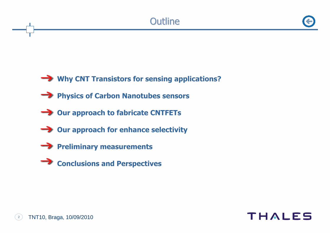
Why CNT Transistors for sensing applications?
Physics of Carbon Nanotubes sensors
Our approach to fabricate CNTFETs
Our approach for enhance selectivity
Preliminary measurements
Conclusions and Perspectives
OutlineOutline
3 TNT10, Braga, 10/09/2010
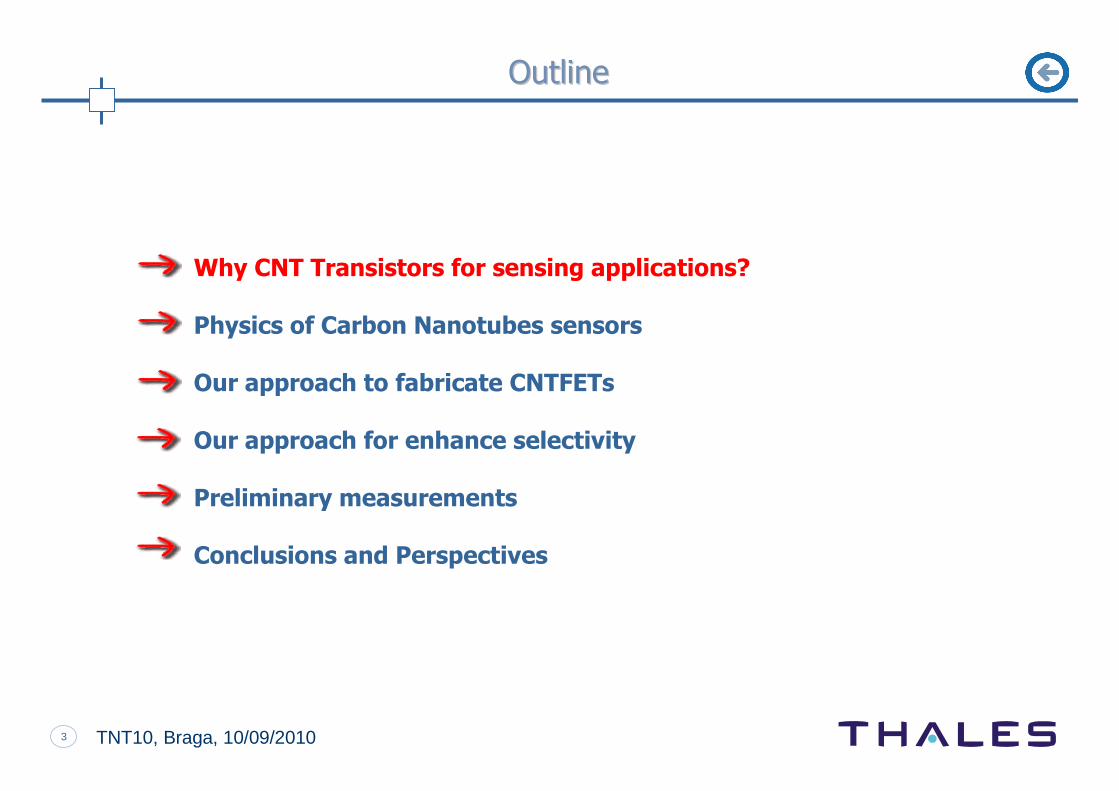
Why CNT Transistors for sensing applications?
Physics of Carbon Nanotubes sensors
Our approach to fabricate CNTFETs
Our approach for enhance selectivity
Preliminary measurements
Conclusions and Perspectives
OutlineOutline
4 TNT10, Braga, 10/09/2010
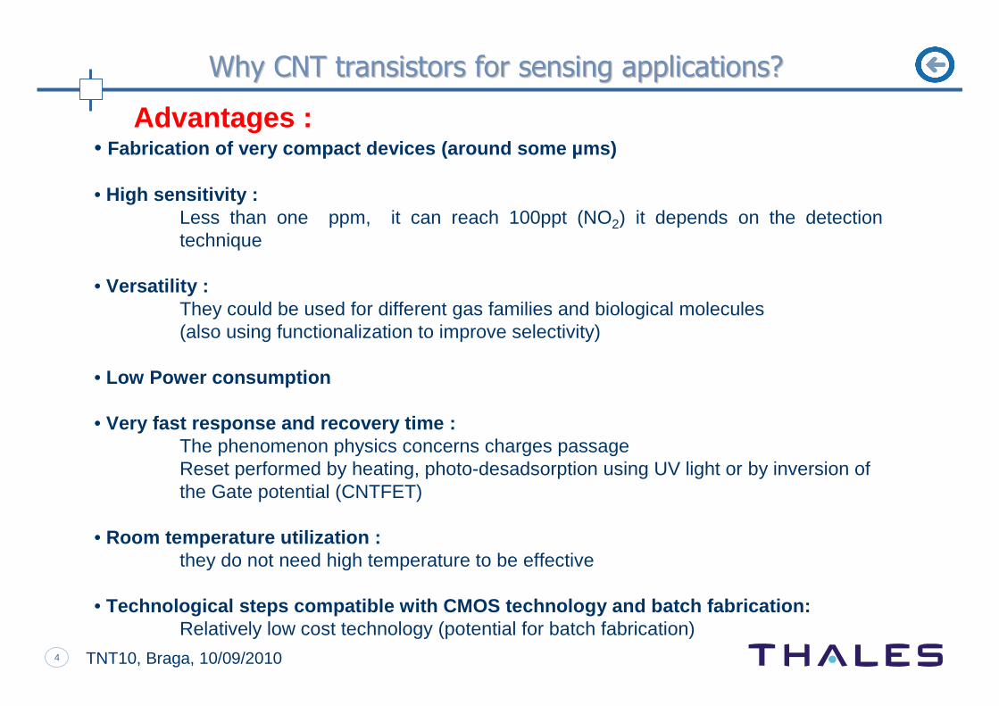
Advantages :• Fabrication of very compact devices (around some µm s)
• High sensitivity :Less than one ppm, it can reach 100ppt (NO2) it depends on the detection technique
• Versatility : They could be used for different gas families and biological molecules (also using functionalization to improve selectivity)
• Low Power consumption
• Very fast response and recovery time :The phenomenon physics concerns charges passageReset performed by heating, photo-desadsorption using UV light or by inversion ofthe Gate potential (CNTFET)
• Room temperature utilization : they do not need high temperature to be effective
• Technological steps compatible with CMOS technology and batch fabrication: Relatively low cost technology (potential for batch fabrication)
Why CNT transistors for sensing applications?Why CNT transistors for sensing applications?

5 TNT10, Braga, 10/09/2010
Why CNT Transistors for sensing applications?
Physics of Carbon Nanotubes sensors
Our approach to fabricate CNTFETs
Our approach for enhance selectivity
Preliminary measurements
Conclusions and Perspectives
OutlineOutline
6 TNT10, Braga, 10/09/2010
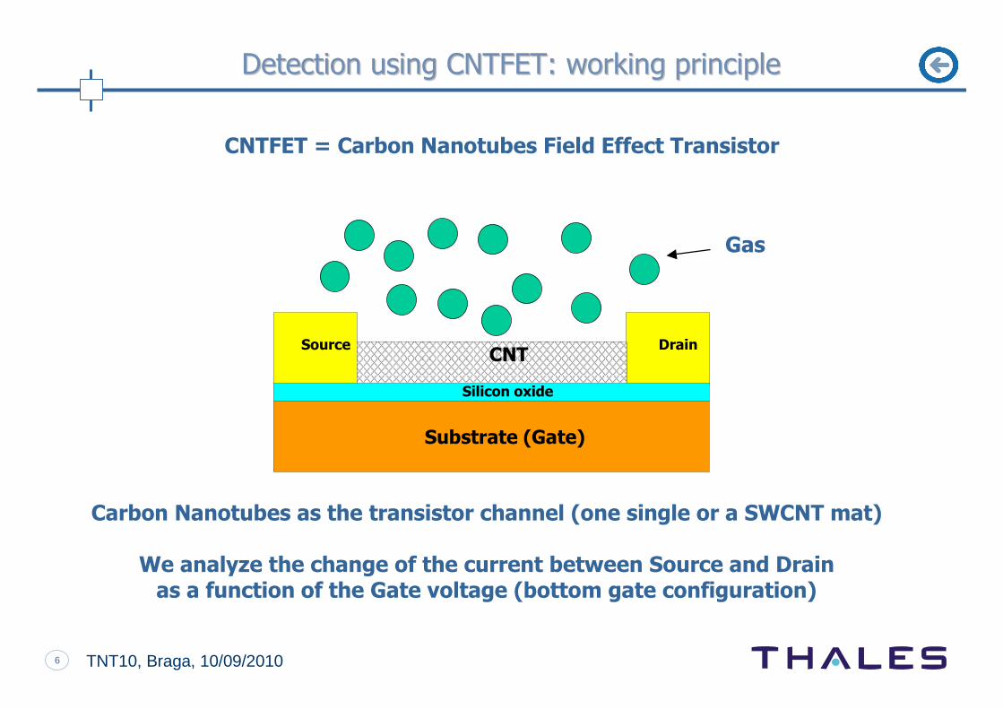
Detection using CNTFET: working principleDetection using CNTFET: working principle
DrainCNTCNT
Source
Silicon oxide
Substrate (Gate)
Carbon Nanotubes as the transistor channel (one single or a SWCNT mat)
We analyze the change of the current between Source and Drainas a function of the Gate voltage (bottom gate configuration)
CNTFET = Carbon Nanotubes Field Effect Transistor
Gas
7 TNT10, Braga, 10/09/2010
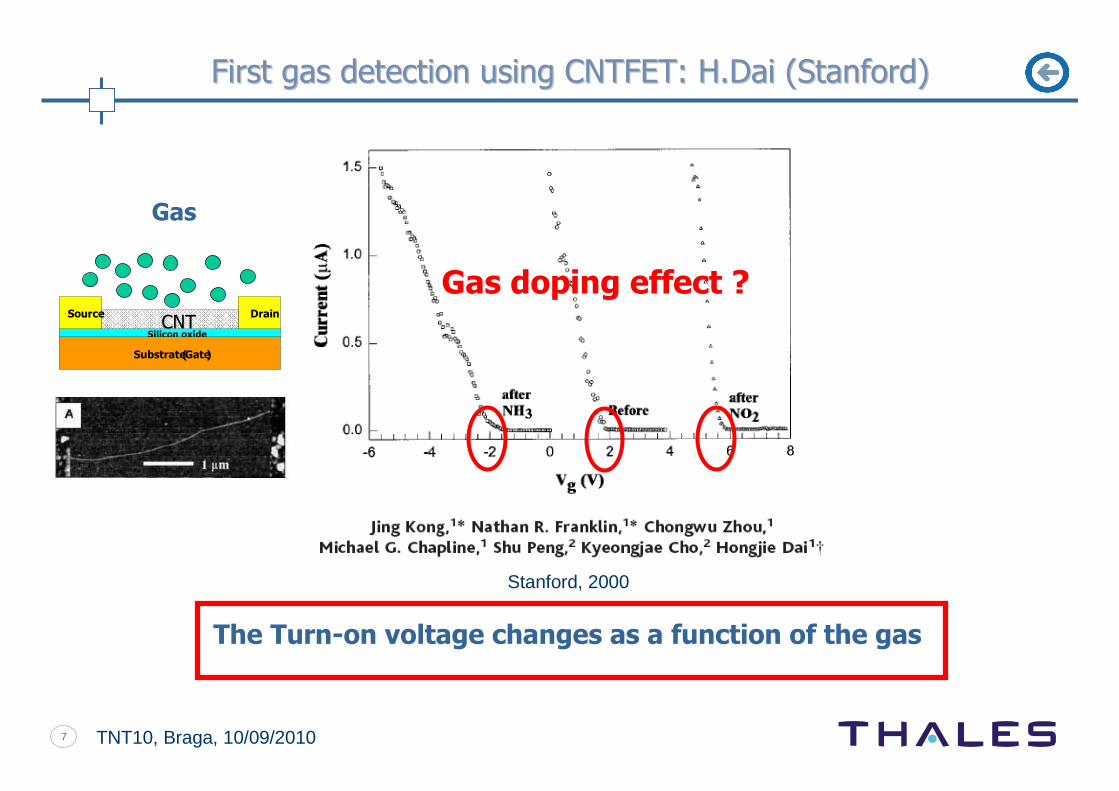
Stanford, 2000
First gas detection using CNTFET: H.Dai (Stanford)First gas detection using CNTFET: H.Dai (Stanford)
Gas doping effect ?
The Turn-on voltage changes as a function of the gas
DrainCNTCNT
Source
Silicon oxide
Substrate(Gate)
Gas
8 TNT10, Braga, 10/09/2010
Drain
CNTCNTSource
Silicon oxide
Substrate ( Gate )
∆R
T
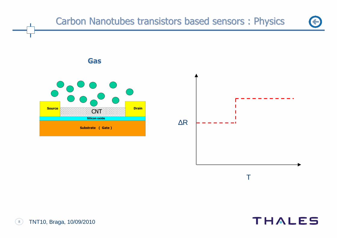
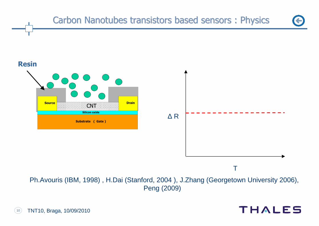
Carbon Nanotubes transistors based sensors : PhysicsCarbon Nanotubes transistors based sensors : Physics
Gas
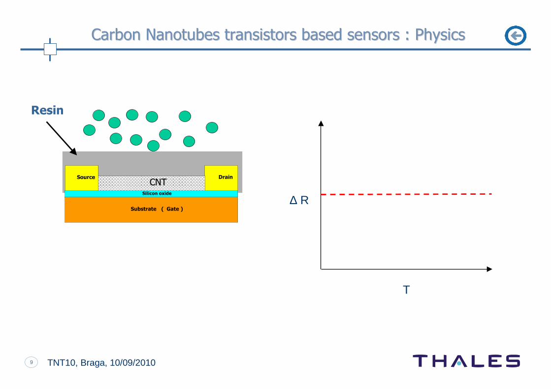
9 TNT10, Braga, 10/09/2010
Drain
CNTCNTSource
Silicon oxide
Substrate ( Gate )
∆ R
T
Carbon Nanotubes transistors based sensors : PhysicsCarbon Nanotubes transistors based sensors : Physics
Resin
10 TNT10, Braga, 10/09/2010
Drain
CNTCNTSource
Silicon oxide
Substrate ( Gate )
∆ R
T
Ph.Avouris (IBM, 1998) , H.Dai (Stanford, 2004 ), J.Zhang (Georgetown University 2006),Peng (2009)
Carbon Nanotubes transistors based sensors : PhysicsCarbon Nanotubes transistors based sensors : Physics
Resin
11 TNT10, Braga, 10/09/2010
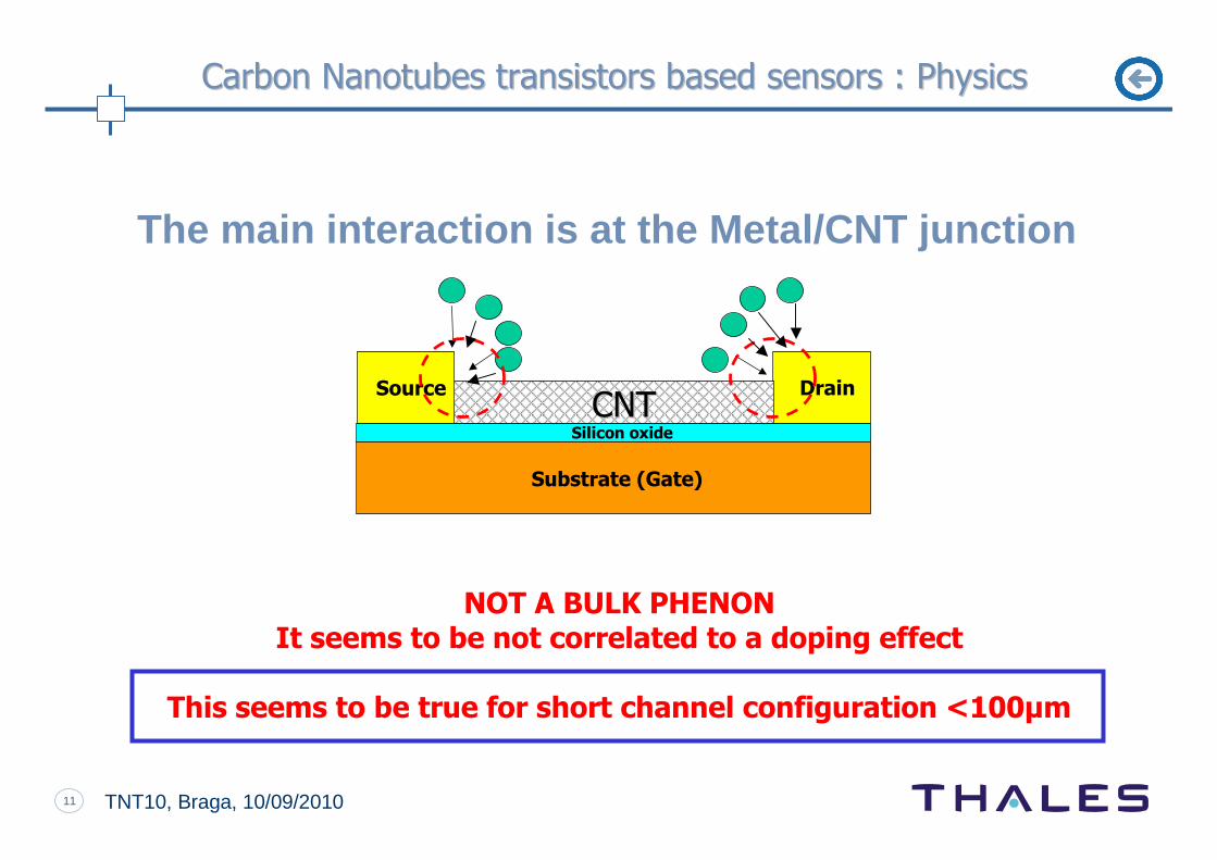
DrainCNTCNT
Source
Silicon oxide
Substrate (Gate)
The main interaction is at the Metal/CNT junction
Carbon Nanotubes transistors based sensors : PhysicsCarbon Nanotubes transistors based sensors : Physics
NOT A BULK PHENONIt seems to be not correlated to a doping effect
This seems to be true for short channel configuration <100µm
12 TNT10, Braga, 10/09/2010
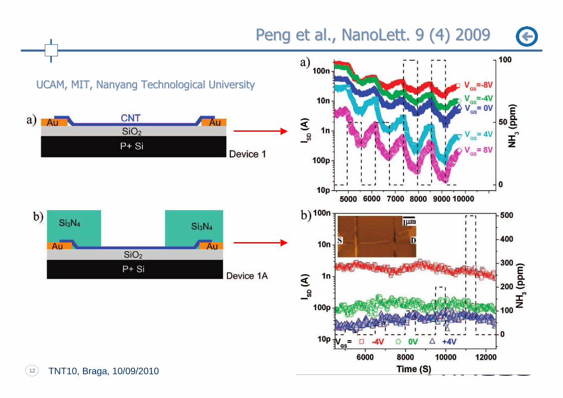
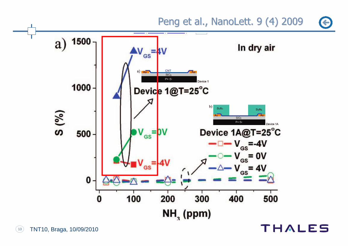
Peng Peng et al., et al., NanoLettNanoLett. 9 (4) 2009. 9 (4) 2009
UCAM, MIT,UCAM, MIT, Nanyang Technological UniversityNanyang Technological University
13 TNT10, Braga, 10/09/2010
Peng Peng et al., et al., NanoLettNanoLett. 9 (4) 2009. 9 (4) 2009
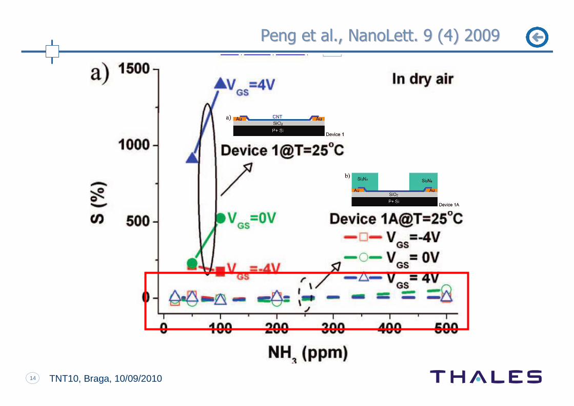
14 TNT10, Braga, 10/09/2010
Peng Peng et al., et al., NanoLettNanoLett. 9 (4) 2009. 9 (4) 2009
15 TNT10, Braga, 10/09/2010
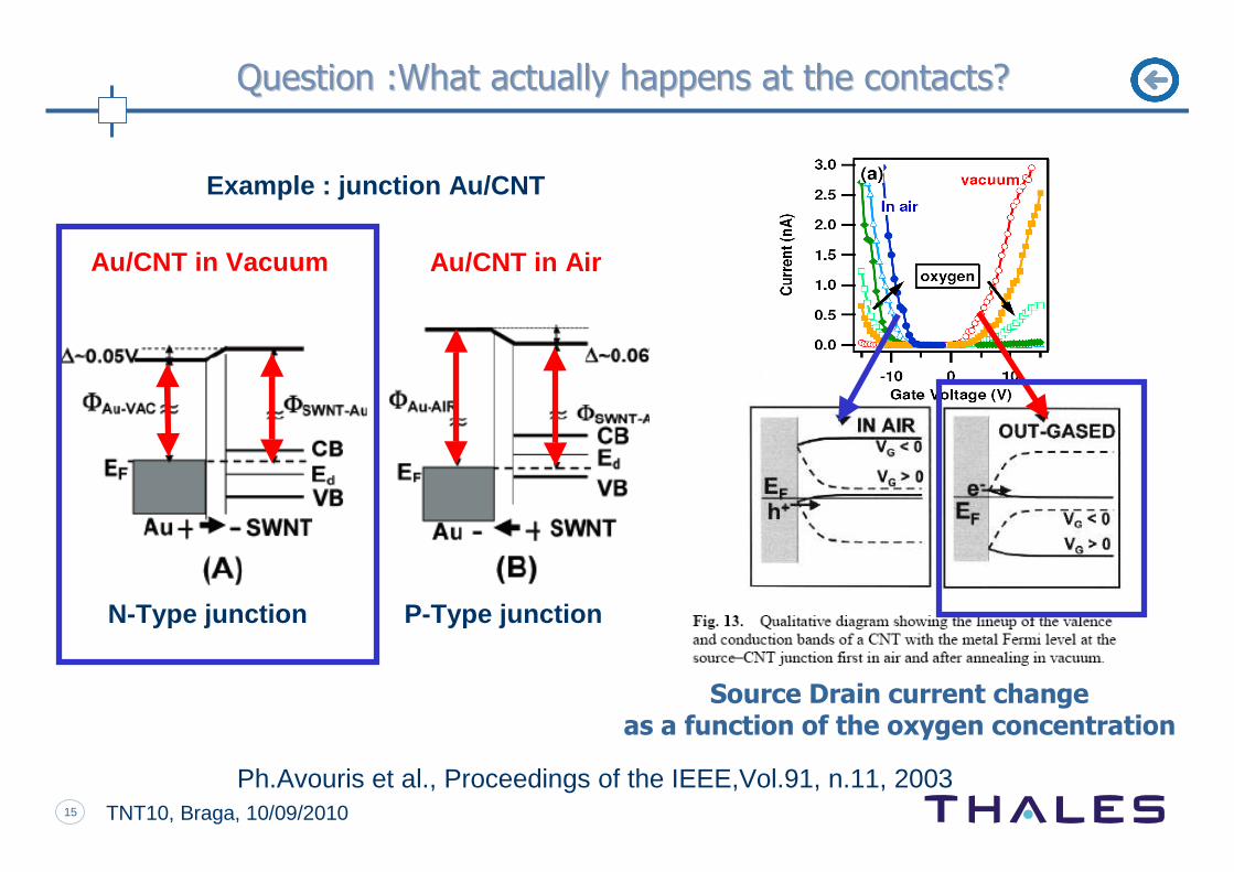
Au/CNT in Vacuum Au/CNT in Air
Ph.Avouris et al., Proceedings of the IEEE,Vol.91, n.11, 2003
N-Type junction P-Type junction
Example : junction Au/CNT
Question :What actually happens at the contacts?Question :What actually happens at the contacts?
Source Drain current change as a function of the oxygen concentration
16 TNT10, Braga, 10/09/2010
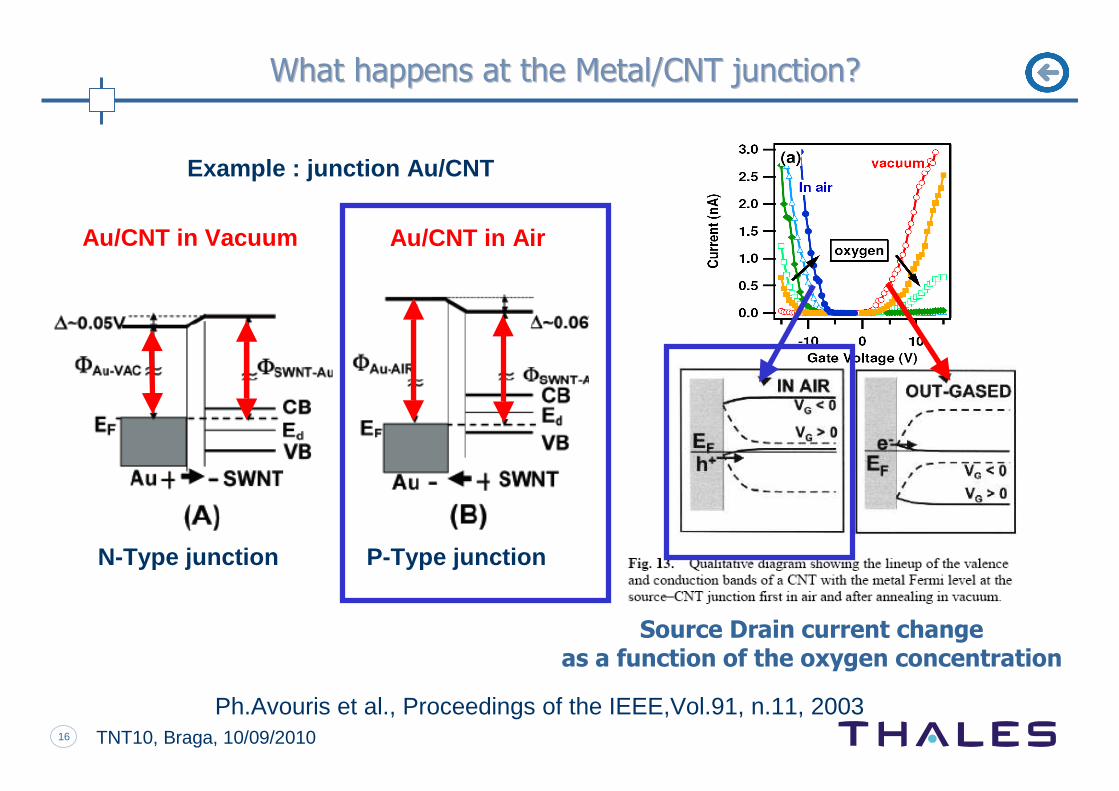
Au/CNT in Vacuum Au/CNT in Air
N-Type junction P-Type junction
Example : junction Au/CNT
What happens at the Metal/CNT junction?What happens at the Metal/CNT junction?
Source Drain current change as a function of the oxygen concentration
Ph.Avouris et al., Proceedings of the IEEE,Vol.91, n.11, 2003
17 TNT10, Braga, 10/09/2010
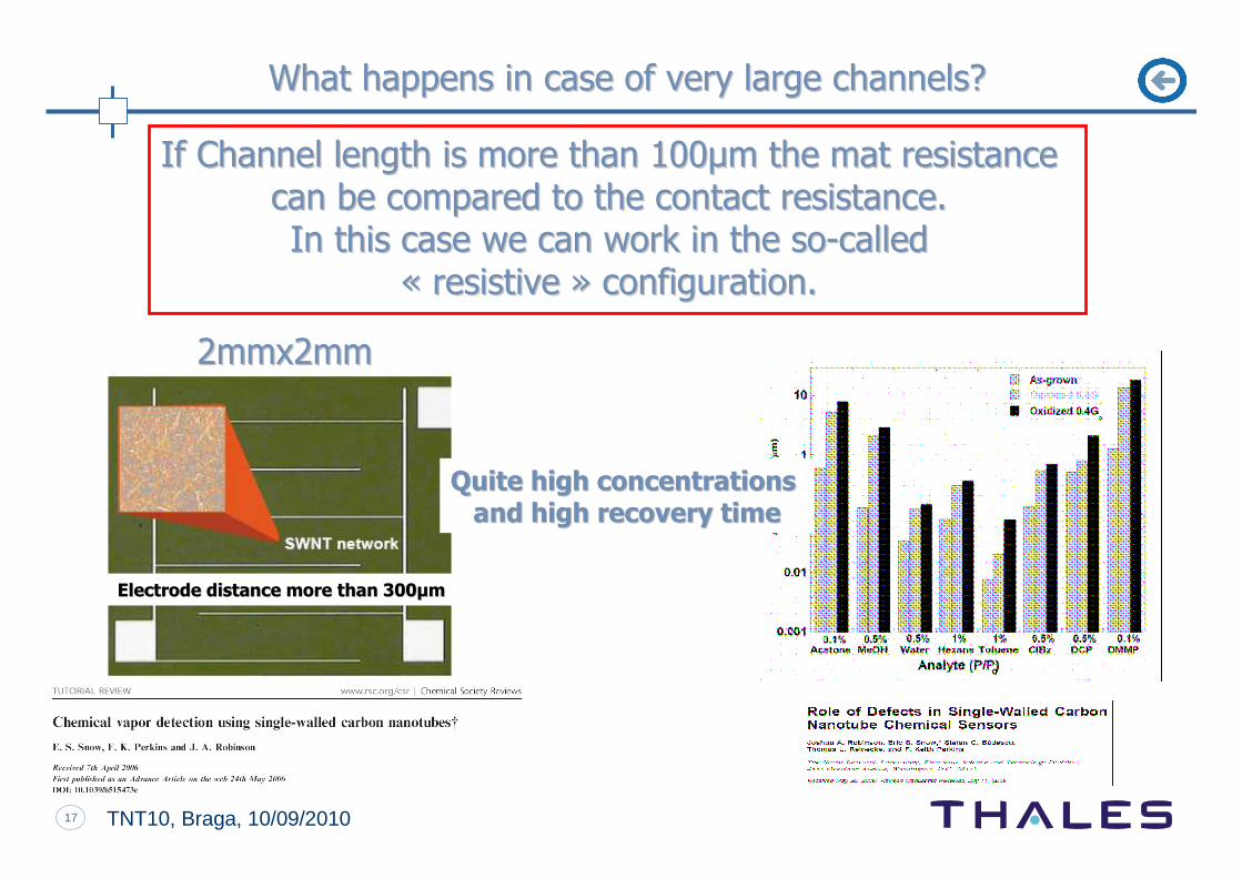
What happens in case of very large channels?What happens in case of very large channels?
If Channel length is more than 100µm the mat resistance If Channel length is more than 100µm the mat resistance
can be compared to the contact resistance.can be compared to the contact resistance.
In this case we can work in the soIn this case we can work in the so--called called
«« resistiveresistive » configuration.» configuration.
2mmx2mm2mmx2mm
Electrode Electrode distance more distance more than than 300µm300µm
Quite high Quite high concentrations concentrations
and high recovery and high recovery timetime
18 TNT10, Braga, 10/09/2010
Why CNT Transistors for sensing applications?
Physics of Carbon Nanotubes sensors
Our approach to fabricate CNTFETs
Our approach for enhance selectivity
Preliminary measurements
Conclusions and Perspectives
OutlineOutline
19 TNT10, Braga, 10/09/2010
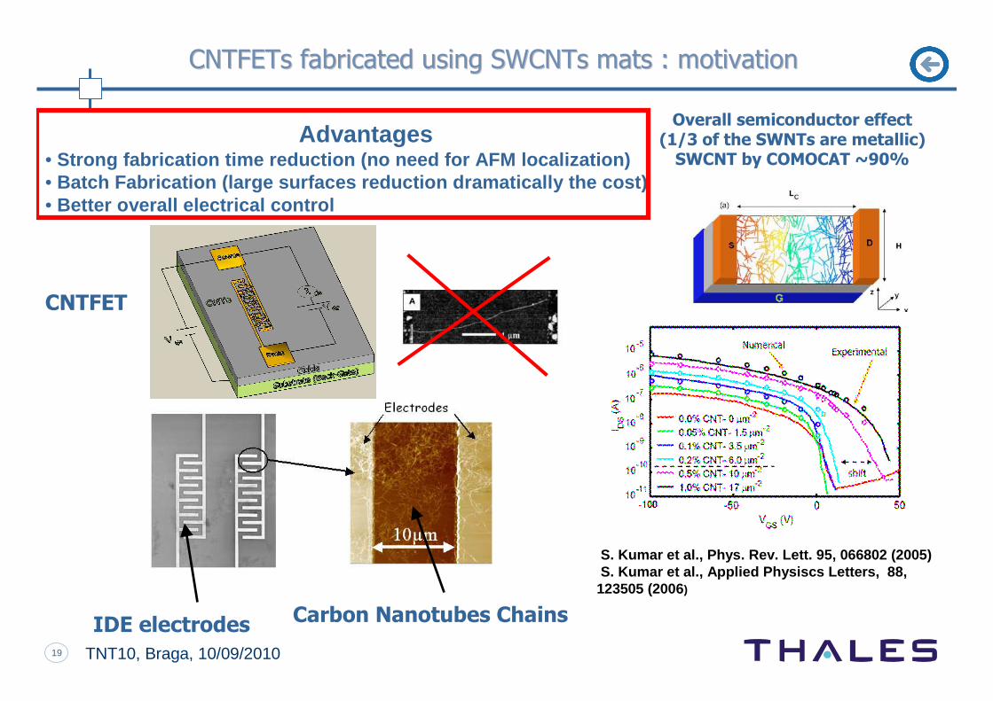
CNTFETs fabricated using CNTFETs fabricated using SWCNTs SWCNTs mats : motivation mats : motivation
S. Kumar et al., Phys. Rev. Lett. 95, 066802 (2005)S. Kumar et al., Applied Physiscs Letters, 88,
123505 (2006)
Advantages• Strong fabrication time reduction (no need for AFM localization)• Batch Fabrication (large surfaces reduction dramati cally the cost)• Better overall electrical control
Overall semiconductor effect(1/3 of the SWNTs are metallic)SWCNT by COMOCAT ~90%
CNTFET
Carbon Nanotubes ChainsIDE electrodes
20 TNT10, Braga, 10/09/2010
Why CNT Transistors for sensing applications?
Physics of Carbon Nanotubes sensors
Our approach to fabricate CNTFETs
Our approach for enhance selectivity
Preliminary measurements
Conclusions and Perspectives
OutlineOutline
21 TNT10, Braga, 10/09/2010
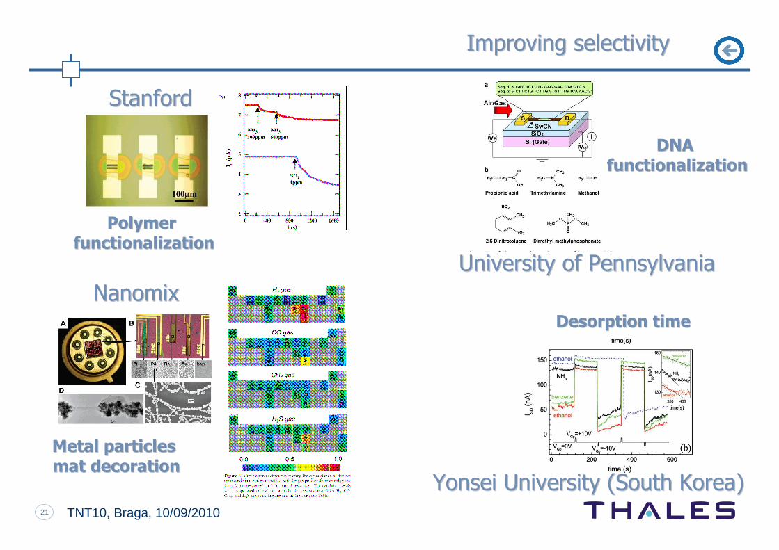
NanomixNanomix
StanfordStanford
University University of of PennsylvaniaPennsylvania
Yonsei University Yonsei University ((SouthSouth KoreaKorea))
Improving selectivityImproving selectivity
Metal particles Metal particles
mat decorationmat decoration
Polymer Polymer
functionalizationfunctionalization
DNA DNA
functionalizationfunctionalization
Desorption timeDesorption time
22 TNT10, Braga, 10/09/2010
Drain Source
Transfer
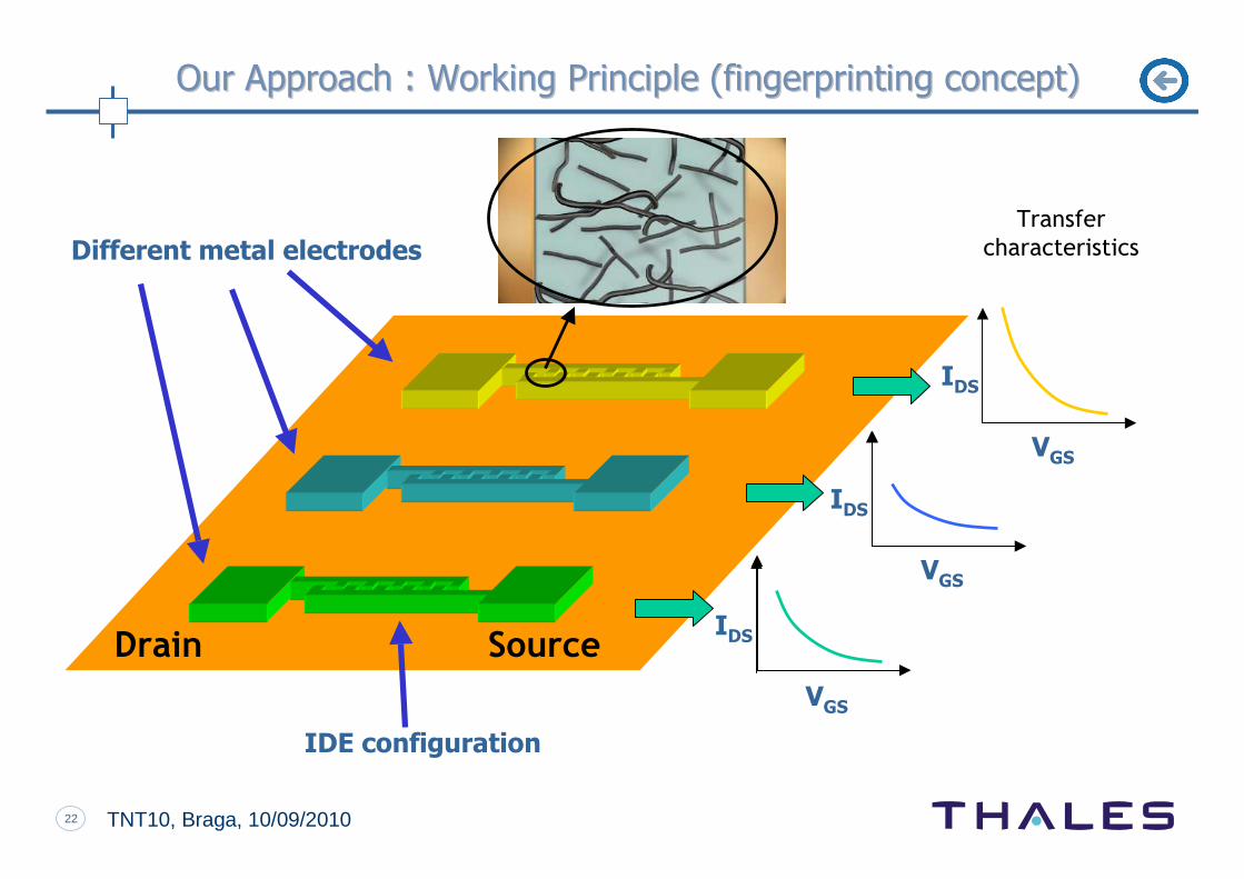
characteristicsDifferent metal electrodes
IDS
VGS
IDS
VGS
IDS
VGS
IDE configuration
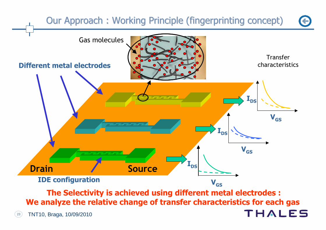
Our Our ApproachApproach : Working : Working Principle Principle ((fingerprintingfingerprinting concept)concept)
23 TNT10, Braga, 10/09/2010
Drain Source
Transfer
characteristics
Our Our ApproachApproach : Working : Working Principle Principle ((fingerprintingfingerprinting concept)concept)
Different metal electrodes
IDS
VGS
IDS
VGS
IDS
VGSIDE configuration
Gas molecules
The Selectivity is achieved using different metal electrodes :We analyze the relative change of transfer characteristics for each gas
24 TNT10, Braga, 10/09/2010
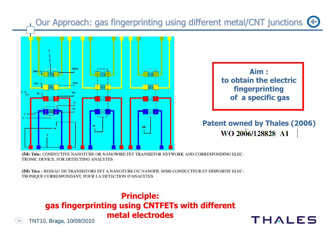
Our Approach: gas fingerprinting using different metal/CNT junctOur Approach: gas fingerprinting using different metal/CNT junctionsions
Principle: gas fingerprinting using CNTFETs with different
metal electrodes
Aim : to obtain the electric
fingerprinting of a specific gas
Patent owned by Thales (2006)
25 TNT10, Braga, 10/09/2010
Introduction : Nanocarb Lab. presentation
Why CNT Transistors for sensing applications?
Physics of Carbon Nanotubes sensors
Our approach to enhance selectivity
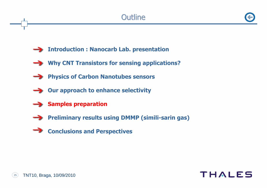
Samples preparation
Preliminary results using DMMP (simili-sarin gas)
Conclusions and Perspectives
OutlineOutline
26 TNT10, Braga, 10/09/2010
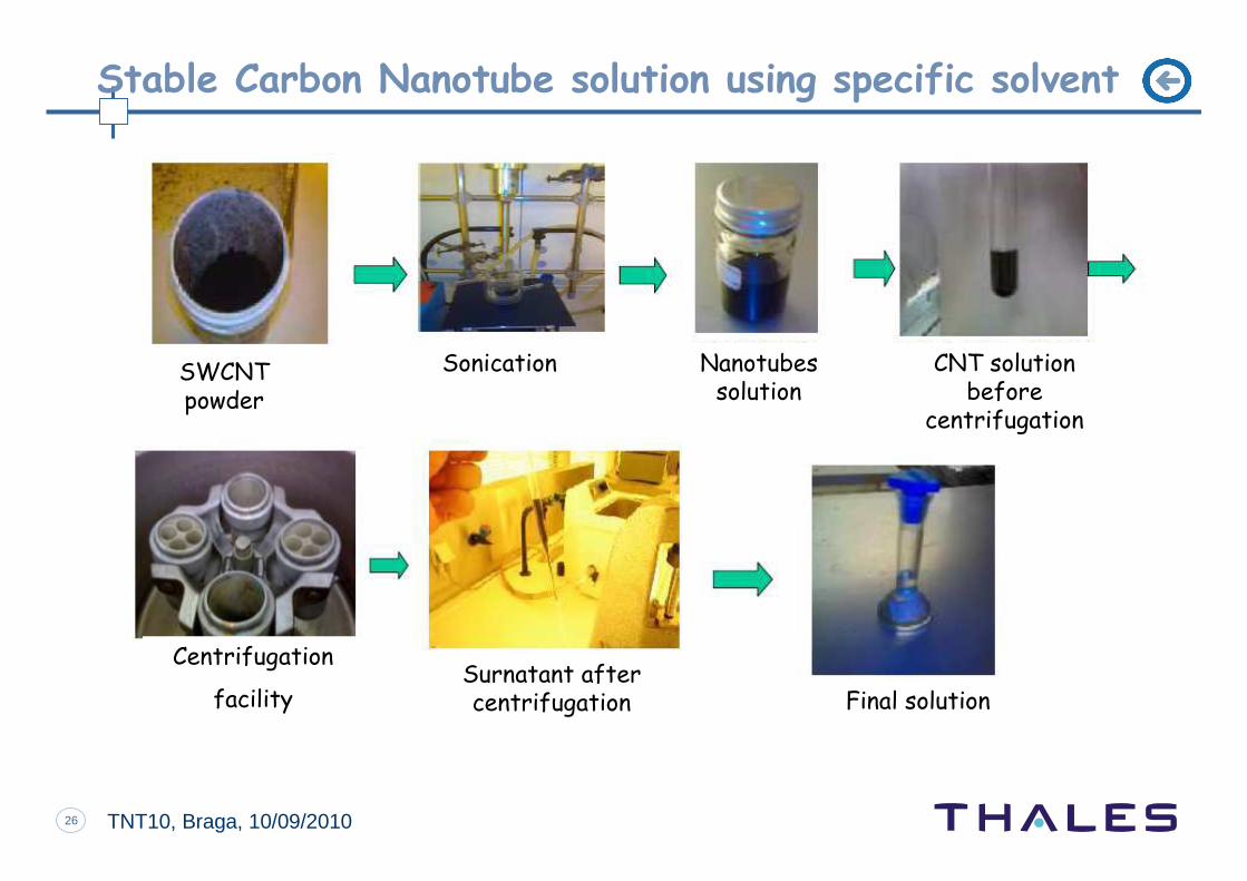
Sonication Nanotubes solution
CNT solution before
centrifugation
Centrifugation
facilitySurnatant after centrifugation Final solution
SWCNT powder
Stable Carbon Nanotube solution using specific solvent
27 TNT10, Braga, 10/09/2010
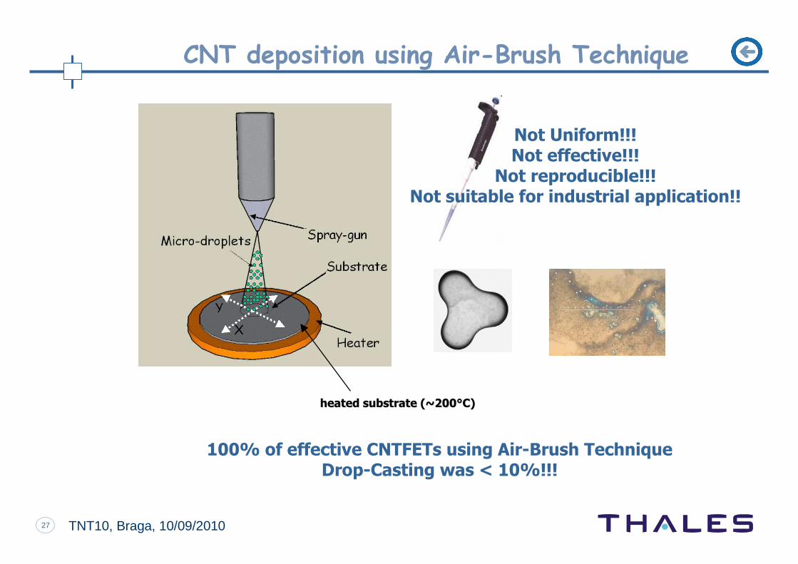
CNT deposition using Air-Brush Technique
heated substrate (~200°C)heated substrate (~200°C)
100% of effective CNTFETs using Air-Brush TechniqueDrop-Casting was < 10%!!!
Not Uniform!!!Not effective!!!
Not reproducible!!!Not suitable for industrial application!!
28 TNT10, Braga, 10/09/2010
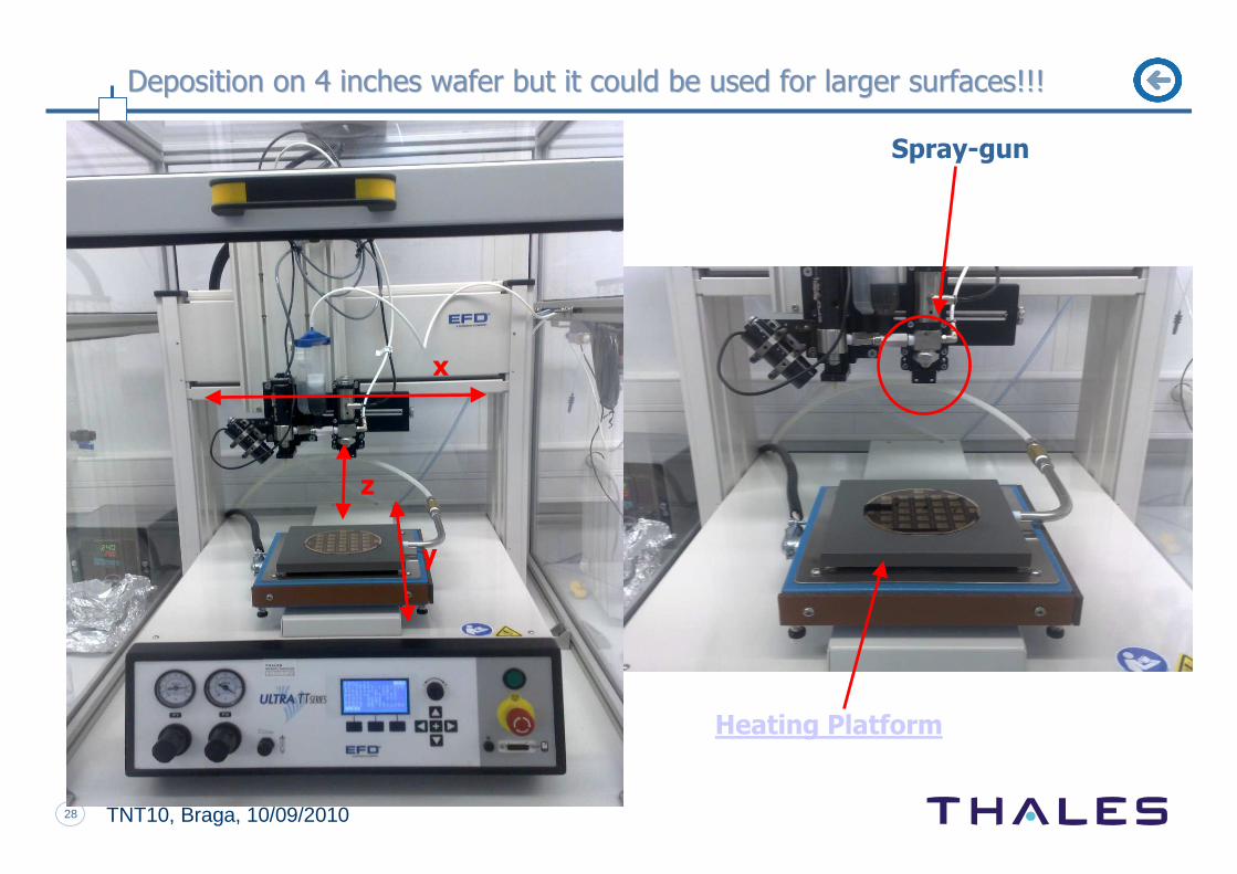
Deposition on 4 inches wafer but it could be used for larger surDeposition on 4 inches wafer but it could be used for larger surfaces!!!faces!!!
Spray-gun
Heating Platform
z
y
x
29 TNT10, Braga, 10/09/2010
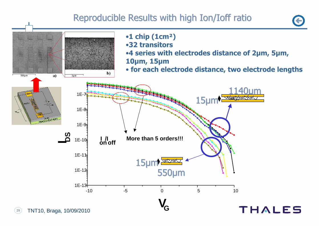
Reproducible Results with high Ion/Reproducible Results with high Ion/IoffIoff ratioratio
-10 -5 0 5 101E-13
1E-12
1E-11
1E-10
1E-9
1E-8
1E-7
Ion
/Ioff
More than 5 orders!!!I DS
VG
1140µm1140µm
550µm550µm15µm15µm
15µm15µm
•1 chip (1cm²) •32 transitors •4 series with electrodes distance of 2µm, 5µm, 10µm, 15µm • for each electrode distance, two electrode lengths
30 TNT10, Braga, 10/09/2010
Why CNT Transistors for sensing applications?
Physics of Carbon Nanotubes sensors
Our approach to fabricate CNTFETs
Our approach for enhance selectivity
Preliminary measurements
Conclusions and Perspectives
OutlineOutline
31 TNT10, Braga, 10/09/2010
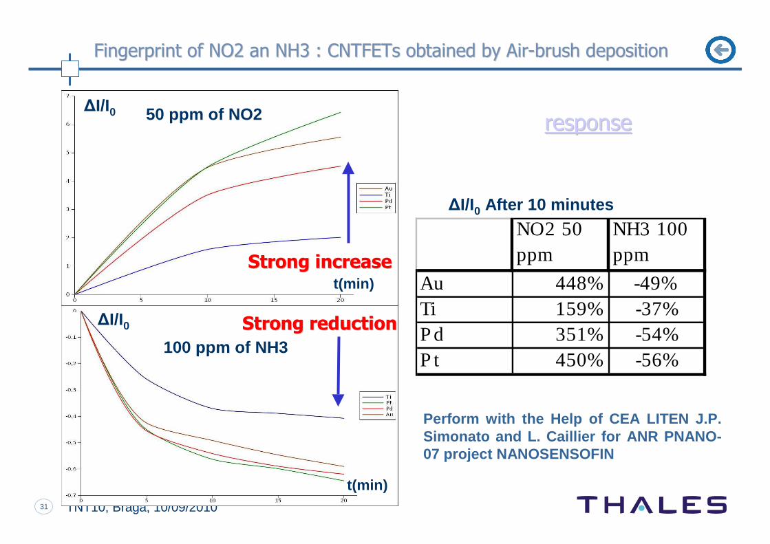
Fingerprint of NO2 an NH3 : CNTFETs obtained by AirFingerprint of NO2 an NH3 : CNTFETs obtained by Air--brush depositionbrush deposition
∆I/I0
∆I/I0
t(min)
t(min)
100 ppm of NH3
50 ppm of NO2
NO2 50 ppm
NH3 100 ppm
Au 448% -49%Ti 159% -37%P d 351% -54%P t 450% -56%
∆I/I0 After 10 minutes
Perform with the Help of CEA LITEN J.P. Simonato and L. Caillier for ANR PNANO-07 project NANOSENSOFIN
Strong increaseStrong increase
Strong reductionStrong reduction
responseresponse
32 TNT10, Braga, 10/09/2010
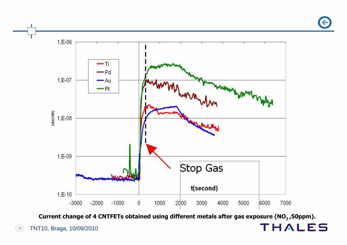
Current change of 4 CNTFETs obtained using different metals after gas exposure (NO2 ,50ppm).
33 TNT10, Braga, 10/09/2010
Why CNT Transistors for sensing applications?
Physics of Carbon Nanotubes sensors
Our approach to fabricate CNTFETs
Our approach for enhance selectivity
Preliminary measurements
Conclusions and Perspectives
OutlineOutline
34 TNT10, Braga, 10/09/2010
Conclusions and perspectivesConclusions and perspectives
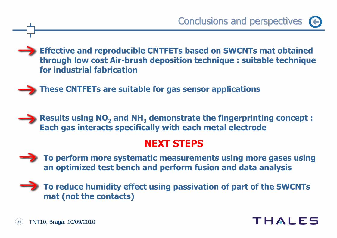
Effective and reproducible CNTFETs based on SWCNTs mat obtained through low cost Air-brush deposition technique : suitable technique for industrial fabrication
These CNTFETs are suitable for gas sensor applications
Results using NO2 and NH3 demonstrate the fingerprinting concept :Each gas interacts specifically with each metal electrode
To perform more systematic measurements using more gases using an optimized test bench and perform fusion and data analysis
To reduce humidity effect using passivation of part of the SWCNTs mat (not the contacts)
NEXT STEPS
35 TNT10, Braga, 10/09/2010
Thank you for your attention!Thank you for your attention!
Recent publicationsCarbon Nanotubes based transistors composed of single-walled carbon nanotubes mats as gas sensors : a review, P.Bondavalli, Comptes Rendus de Physique, in press (2010)
CNTFETs based gas sensors : patent review, P. Bondavalli, Recent Patents on Electrical Engineering, 3 (2010)
CNTFET based gas sensors : State of the art and critical review, P.Bondavalli, P.Legagneux and D.Pribat, Sensors and Actuators B, Volume 140, Issue 1, 18 June 2009, Pages 304-318
![Clinical data successes - Joseph Paul Cohen...cat = [0 0 1 0 0 0 0 0 0 0 0 0 0 0 … 0] dog = [0 0 0 0 1 0 0 0 0 0 0 0 0 0 … 0] house = [1 0 0 0 0 0 0 0 0 0 0 0 0 0 … 0] Note!](https://img.pdfslide.us/doc/110x75/5fdf222a2dd17b0d95129a68/clinical-data-successes-joseph-paul-cohen-cat-0-0-1-0-0-0-0-0-0-0-0-0-0.jpg)


![[XLS] · Web view1101 0 0 0 0 11 0 0 12 0 0 13 0 0 14 0 0 15 0 0 16 0 0 17 0 0 18 0 0 19 0 0 51 1 1 0 0 81 2 0 0 3 0 0 0 0 0 0 0 0 0 0 0 0 0 0 0 0 0 1 1 0 0 2 0 0 3 0 0 0 0 0 0 0](https://img.pdfslide.us/doc/110x75/5ae8b1767f8b9a8b2b905346/xls-view1101-0-0-0-0-11-0-0-12-0-0-13-0-0-14-0-0-15-0-0-16-0-0-17-0-0-18-0-0-19.jpg)


![[XLS] · Web view0 0 0 0 0 0 0 0 0 0 0 0 0 0 0 0 0 0 0 0 0 0 0 0 7 2 0 0 0 0 0 0 0 0 0 0 0 5 4 0 0 0 0 0 0 0 0 0 0 0 5 4 0 0 0 0 0 0 0 0 0 0 0 5 4 0 0 0 0 0 0 0 0 0 0 0 5 4 0 0 0 0](https://img.pdfslide.us/doc/110x75/5aad015d7f8b9a8d678d9907/xls-view0-0-0-0-0-0-0-0-0-0-0-0-0-0-0-0-0-0-0-0-0-0-0-0-7-2-0-0-0-0-0-0-0-0-0.jpg)


![[XLS]mams.rmit.edu.aumams.rmit.edu.au/urs1erc4d2nv1.xlsx · Web view0. 0. 0. 0. 0. 0. 0. 0. 0. 0. 0. 0. 0. 0. 0. 0. 0. 0. 0. 0. 0. 0. 0. 0. 0. 0. 0. 0. 0. 0. 0. 0. 0. 0. 0. 0. 0](https://img.pdfslide.us/doc/110x75/5ab434027f8b9a0f058b8cff/xlsmamsrmitedu-view0-0-0-0-0-0-0-0-0-0-0-0-0-0-0-0-0-0-0.jpg)