Embed Size (px)
Citation preview
CONTENTS
1. SAFETY PRECAUTIONS 1
2. PREVENTION OF ELECTRO STATIC DISCHARGE(ESD)TO ELECTROSTATICALLY
SENSITIVE(ES)DEVICES 1
4. PREVERTION OF STATIC ELECTRICITY DISCHARGE 3
5. ASSEMBLING AND DISASSEMBLING THE MECHANISM UNIT 4
5.1 OPTICAL PICKUP UNIT EXPLOSED VIEW AND PART LIST 4
6. ELECTRICAL CONFIRMATION 7
6.1 VIDEO OUTPUT (LUMINANCE SIGNAL) CONFIRMATION 7
6.2 VIDEO OUTPUT(CHROMINANCE SIGNAL) CONFIRMATION 8
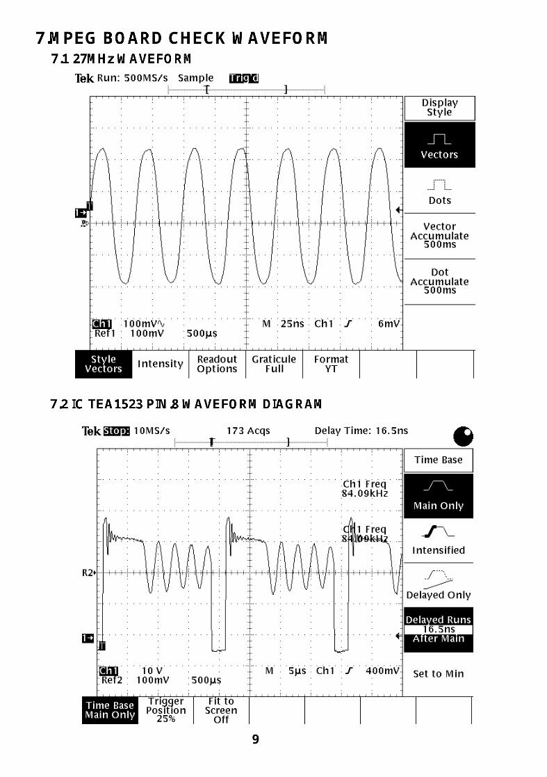
7. MPEG BOARD CHECK WAVEFORM 9
8. IC BLOCK DIAGRAM & DESCRIPTION 10
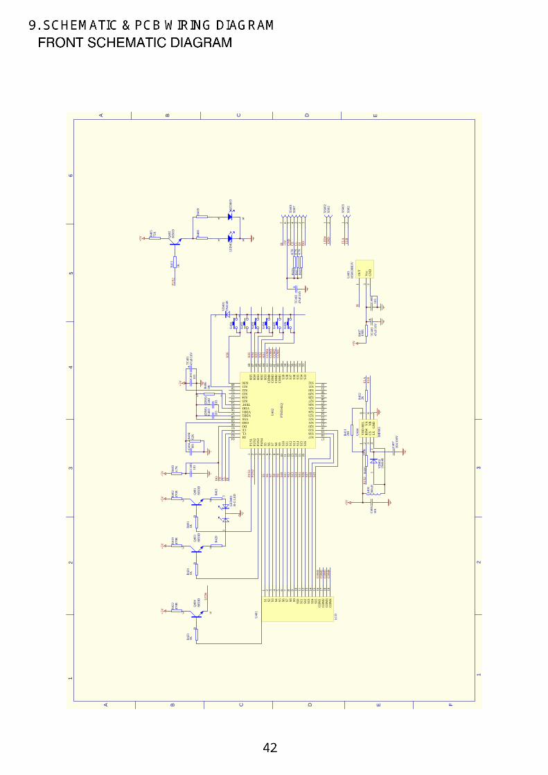
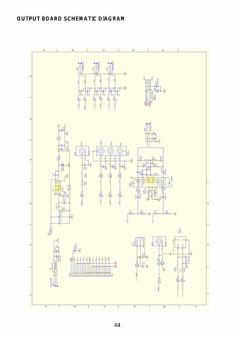
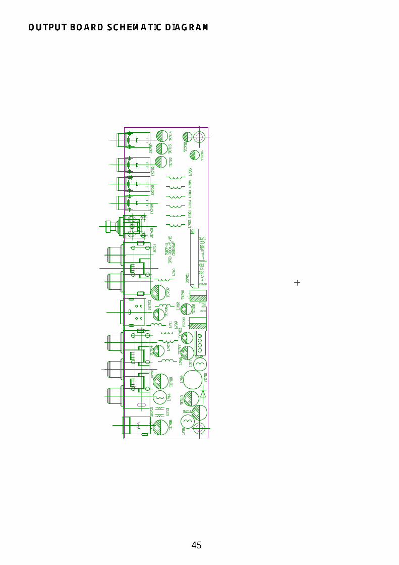
9. SCHEMATIC & PCB WIRING DIAGRAM 42
10. SPARE PARTS LIST 57
8.1 MT1336 10
8.2 MT1379 18
8.3 AM29LV160D 34
8.4 HY57V641620HG 39
3. CONTROL BUTTON LOCATIONS AND EXPLANATIONS 2
5.2 MISCELLANEOUS 6
1.1 GENERAL GUIDELINES1. When servicing, observe the original lead dress. if a short circuit is found, replace all parts which have been overheated or damaged by the short circuit.2. After servicing, see to it that all the protective devices such as insulation barrier, insulation papersshields are properly installed.3. After servicing, make the following leakage current checks to prevent the customer from being exposed
to shock hazards.
Some semiconductor(solid state)devices can be damaged easily by static electricity. Such components commonly are called Electrostatically Sensitive(ES)Devices. Examples of typical ES devices are integratedcircuits and some field-effect transistors and semiconductor chip components. The following techniques should be used to help reduce the incidence of component damage caused by electro static discharge(ESD).1. Immediately before handling any semiconductor component or semiconductor-equipped assembly, drainoff any ESD on your body by touching a known earth ground. Alternatively, obtain and wear a commercially availabel discharging ESD wrist strap, which should be removed for potential shock reasons prior toapplying power to the unit under test.2. After removing an electrical assembly equipped with ES devices,place the assembly on a conductive surface such as alminum foil, to prevent electrostatic charge buildup or exposure of the assembly.3. Use only a grounded-tip soldering iron to solder or unsolder ES devices.4. Use only an anti-static solder removal device. Some solder removal devices not classified as anti-static(ESD protected)can generate electrical charge sufficient to damage ES devices.5. Do not use freon-propelled chemicals. These can generate electrical charges sufficient to damage ESdevices.6. Do not remove a replacement ES device from its protective package until immediately before you areready to install it. (Most replacement ES devices are packaged with leads electrically shorted together by conductive foam, alminum foil or comparable conductive material).7. Immediately before removing the protective material from the leads of a replacement ES device, touchthe protective material to the chassis or circuit assembly into which the device will be installed.CautionBe sure no power is applied to the chassis or circuit, and observe all other safety precautions.8. Minimize bodily motions when handling unpackaged replacement ES devices. (Otherwise harmless motionsuch as the brushing together of your clothes fabric or the lifting of your foot from a carpeted floor cangenerate static electricity(ESD).
notice (1885x323x2 tiff)

Front Panel I l lus t rat ion
54 6 7 92
5
6
4 OPEN/CLOSE button
PLAY/PAUSE button
STOP button
3
7
8
PREV button
NEXT button
POWER switch9
2
3
Power indicator
IR SENSOR
Display window
8
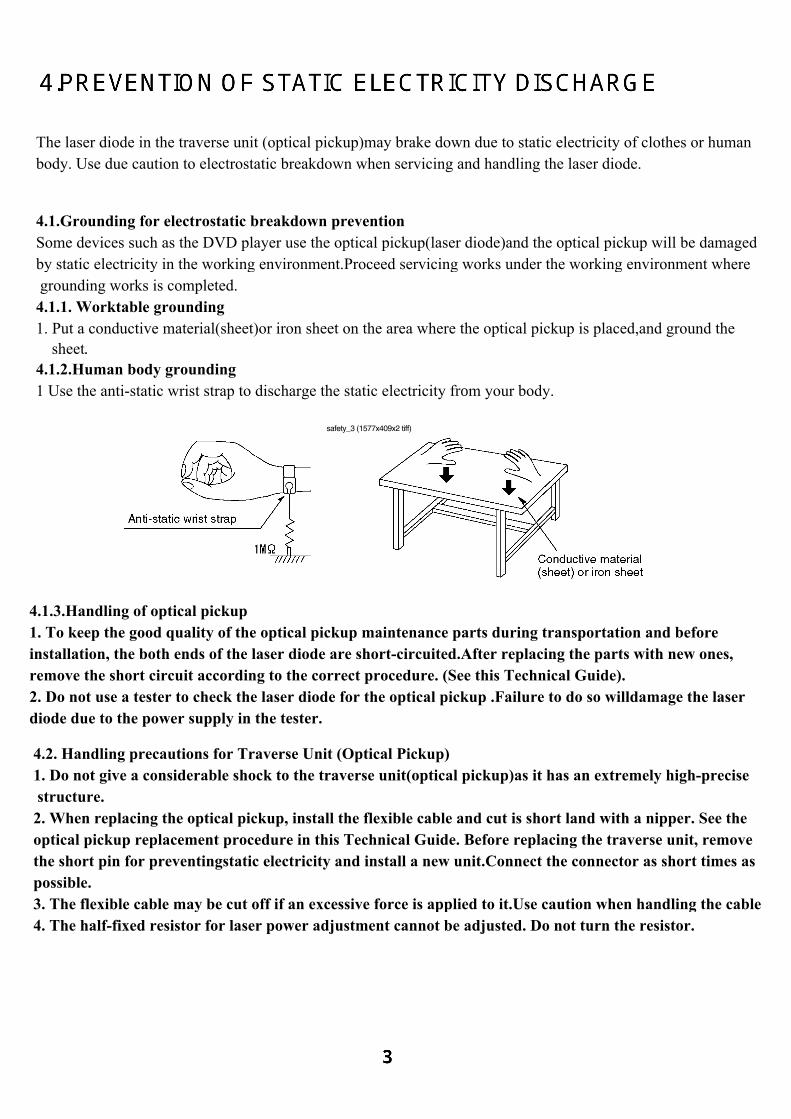
The laser diode in the traverse unit (optical pickup)may brake down due to static electricity of clothes or human body. Use due caution to electrostatic breakdown when servicing and handling the laser diode.
4.1.Grounding for electrostatic breakdown preventionSome devices such as the DVD player use the optical pickup(laser diode)and the optical pickup will be damaged by static electricity in the working environment.Proceed servicing works under the working environment where grounding works is completed.4.1.1. Worktable grounding1. Put a conductive material(sheet)or iron sheet on the area where the optical pickup is placed,and ground the
4.1.2.Human body grounding1 Use the anti-static wrist strap to discharge the static electricity from your body.
4.1.3.Handling of optical pickup1. To keep the good quality of the optical pickup maintenance parts during transportation and beforeinstallation, the both ends of the laser diode are short-circuited.After replacing the parts with new ones,remove the short circuit according to the correct procedure. (See this Technical Guide).2. Do not use a tester to check the laser diode for the optical pickup .Failure to do so willdamage the laserdiode due to the power supply in the tester.
4.2. Handling precautions for Traverse Unit (Optical Pickup)1. Do not give a considerable shock to the traverse unit(optical pickup)as it has an extremely high-precise structure.2. When replacing the optical pickup, install the flexible cable and cut is short land with a nipper. See the optical pickup replacement procedure in this Technical Guide. Before replacing the traverse unit, removethe short pin for preventingstatic electricity and install a new unit.Connect the connector as short times aspossible.3. The flexible cable may be cut off if an excessive force is applied to it.Use caution when handling the cable.4. The half-fixed resistor for laser power adjustment cannot be adjusted. Do not turn the resistor.
safety_3 (1577x409x2 tiff)
sheet.
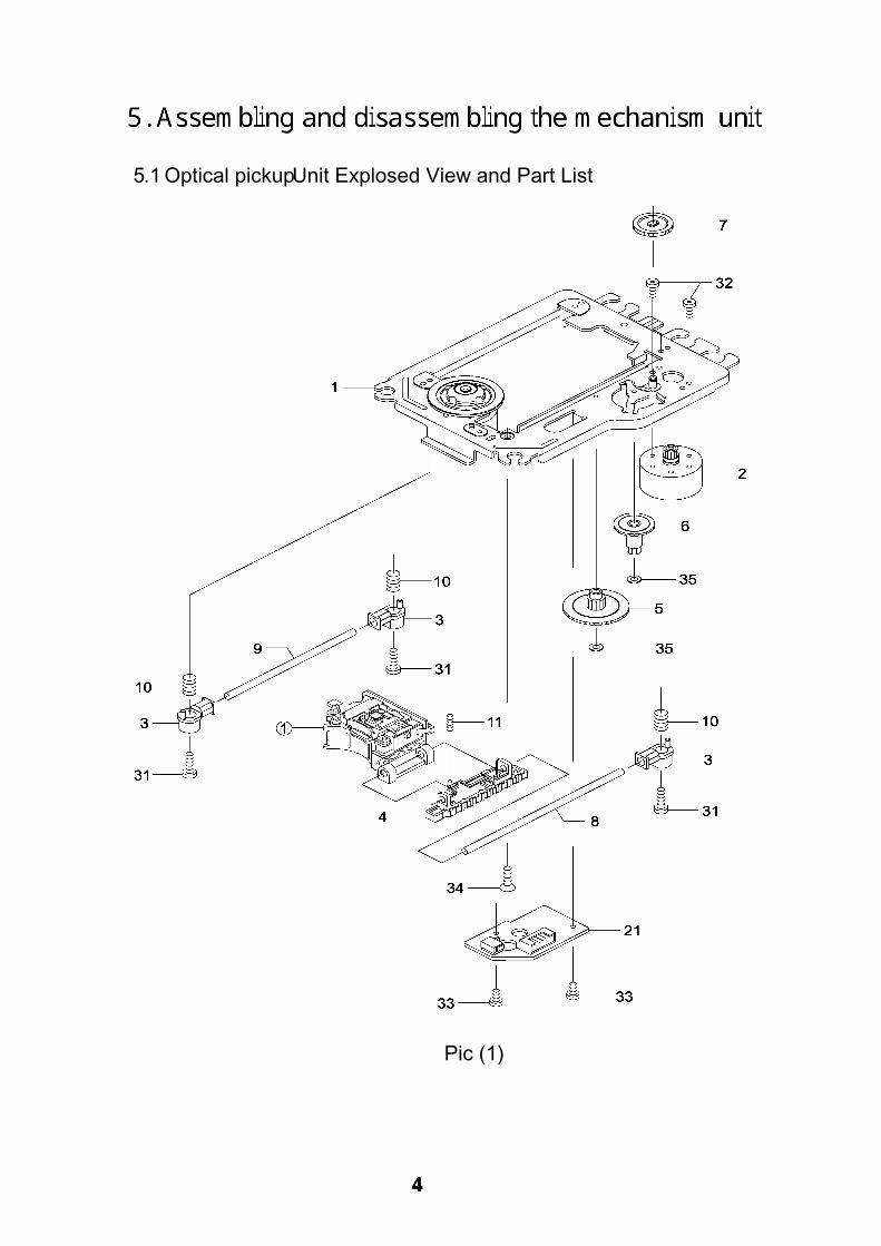
5.1 Optical pickup Unit Explosed View and Part List
Pic (1)
Materials to Pic (1)
No. PARTS CODE PARTS NAME Q ty
14692200 SF-HD60 1 1 1EA0311A06300 ASSY, CHASSIS, COMPLETE 1
2 1EA0M10A15500 ASSY, MOTOR, SLED 1
Or 1EA0M10A15501 ASSY, MOTOR, SLED 1
3 1EA2451A24700 HOLDER, SHAFT 3
4 1EA2511A29100 GEAR, RACK 1
5 1EA2511A29200 GEAR, DRIVE 1
6 1EA2511A29300 GEAR, MIDDLE, A 1
7 1EA2511A29400 GEAR, MIDDLE, B 1
8 1EA2744A03000 SHAFT, SLIDE 1
9 1EA2744A03100 SHAFT, SLIDE, SUB 1
10 1EA2812A15300 SPRING, COMP, TYOUSEI 3
11 1EA2812A15400 SPRING, COMP, RACK 1
21 1EA0B10B20100 ASSY, PWB 1
Or 1EA0B10B20200 ASSY, PWB 1
31 SEXEA25700--- SPECIAL SCREW BIN+-M2X11 3
32 SEXEA25900--- SPECIAL SCREW M1.7X2.2 2
33 SFBPN204R0SE- SCR S-TPG PAN 2X4 2
34 SFSFN266R0SE- SCR S-TPG FLT 2.6X6 1
35 SWXEA15400--- SPECIAL WASHER 1.8X4 X0.25 2
Note : This parts list is not for service parts supply.
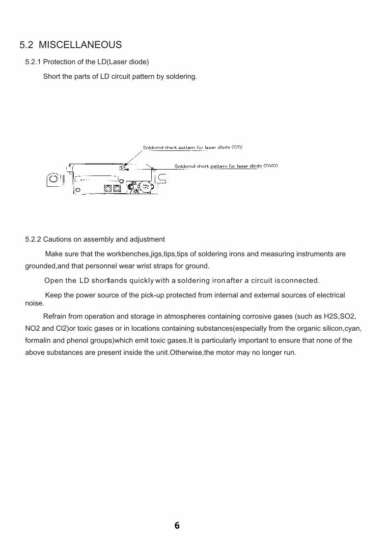
5.2 MISCELLANEOUS
5.2.1 Protection of the LD(Laser diode)
Short the parts of LD circuit pattern by soldering.
5.2.2 Cautions on assembly and adjustment
Make sure that the workbenches,jigs,tips,tips of soldering irons and measuring instruments are
grounded,and that personnel wear wrist straps for ground.
Open the LD short lands quickly with a soldering iron after a circuit is connected.
Keep the power source of the pick-up protected from internal and external sources of electrical noise.
Refrain from operation and storage in atmospheres containing corrosive gases (such as H2S,SO2,
NO2 and Cl2)or toxic gases or in locations containing substances(especially from the organic silicon,cyan,
formalin and phenol groups)which emit toxic gases.It is particularly important to ensure that none of the
above substances are present inside the unit.Otherwise,the motor may no longer run.
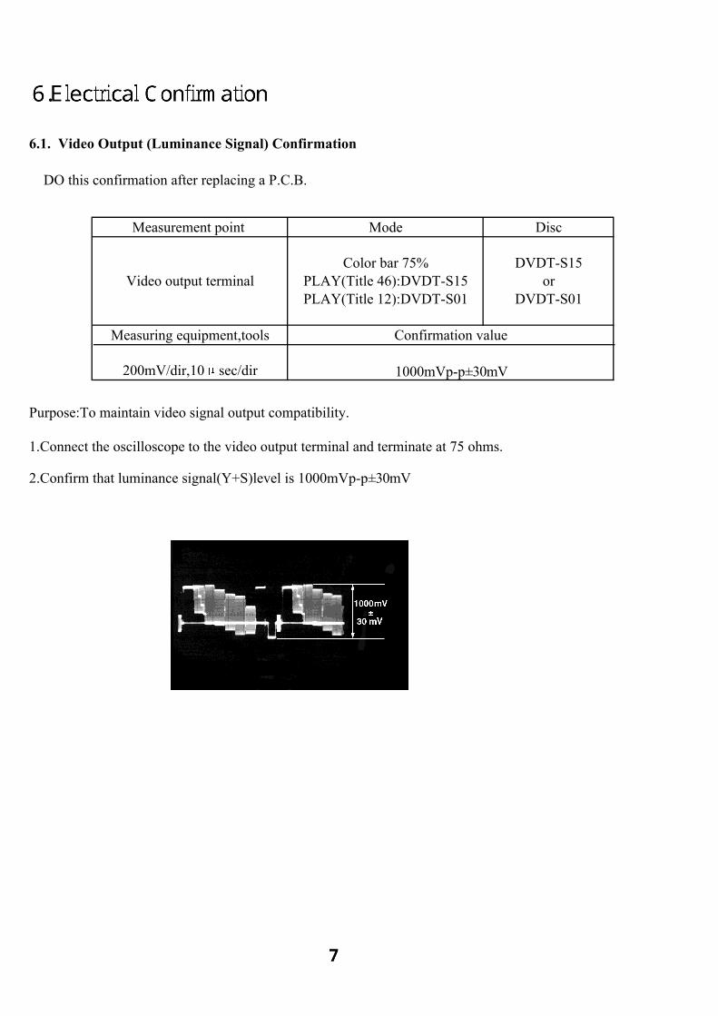
6.1. Video Output (Luminance Signal) Confirmation
DO this confirmation after replacing a P.C.B.
Purpose:To maintain video signal output compatibility.
1.Connect the oscilloscope to the video output terminal and terminate at 75 ohms.
2.Confirm that luminance signal(Y+S)level is 1000mVp-p±30mV
Measurement point
Video output terminalColor bar 75%
PLAY(Title 46):DVDT-S15PLAY(Title 12):DVDT-S01
DVDT-S15or
DVDT-S01
Mode Disc
Measuring equipment,tools
200mV/dir,10 sec/dir 1000mVp-p±30mV
Confirmation value
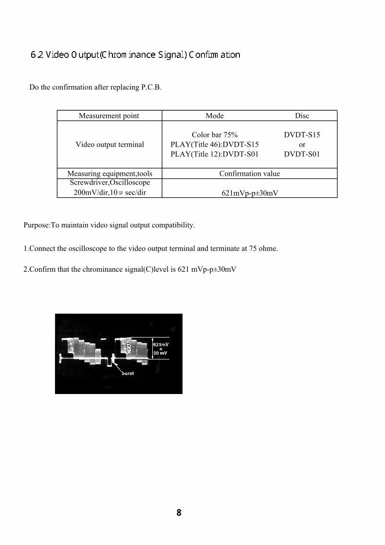
Do the confirmation after replacing P.C.B.
Purpose:To maintain video signal output compatibility.
1.Connect the oscilloscope to the video output terminal and terminate at 75 ohme.
2.Confirm that the chrominance signal(C)level is 621 mVp-p±30mV
Measurement point
Video output terminalColor bar 75%
PLAY(Title 46):DVDT-S15PLAY(Title 12):DVDT-S01
DVDT-S15or
DVDT-S01
Mode Disc
Measuring equipment,tools Confirmation valueScrewdriver,Oscilloscope
200mV/dir,10 sec/dir 621mVp-p±30mV
MT1336 PRELIMINARY, SUBJ ECT TO CHANGE WITHOUT NOTICE MTK CONFIDENTIAL, NO DISCLOSURE
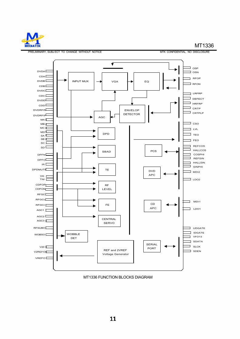
GENERAL DESCRIPTION M T 1 3 3 6 i s a h i g h p e r f o r m a n c e C M O S a n a l o g f r o n t -e n d I C f o r b o t h C D _ R O M d r i v e r u p t o 4 8 X S a n d
D V D - ROM d r i ve r up to 16XS. I t a l so suppo r t s DVD- RAM read up to 4XS Vers ion 2 . I t con ta ins se rvo amp li f ie rs
to genera te focus ing e r ro r , 3-beam t rack ing e r ro r , 1 beam rad ia l push -pu l l s igna l , RF leve l and SBAD fo r servo
func t i ons . I t a l so i nc ludes DPD t rack ing e r ro r s igna l f o r DVD_ROM app l i ca t i on . Fo r DVD- R A M d i s k s , t h e r e a r e
a lso Di f ferent ia l Push-Pu l l (DPP) method for genera t ing t rack ing s igna l and Di f fe rent ia l As t igmat ic Detec t ion
(DAD) fo r p rocess ing focus ing s igna l . P rog rammab le equa l i ze r and AGC c i r cu i t s a re a l so inco rpo ra ted in th i s
ch ip to op t im ize read channe l pe r fo rmance . In add i t i on , th i s ch ip has dua l au tomat ic laser power con t ro l c i rcu i t s
f o r D V D- R O M ( D V D-RAM) and CD -ROM sepe ra te l y and re fe rence vo l t age gene ra to rs t o reduce ex te rna l
componen ts . P rog rammab le f unc t i ons a re imp lemen ted by t he access o f i n te rna l r eg i s te r t h rough b i -d i rec t iona l
serial port to configure modes selection.
FEATURES
n RF equa l i ze r w i t h p rog rammab le cf f r o m 3 M H z t o 7 0 M H z a n d p r o g r a m m a b l e b o o s t f r o m 3 d B t o
13dB.
n MT1336 suppor t s a t l eas t e igh t d i f f e ren t k inds o f p i ck-up heads w i th ve rsa t i l e i npu t con f igu rat ion for
both RF input stages and servo signal blocks.
n Versatile on -line AGC.
n 3 beams tracking error signal generator for CD_ROM application.
n One beam differential phase tracking error (DPD) generator for DVD_ROM application.
n Differential push pull tracki ng error (DPP) generator for DVD_RAM application.
n Focusing error signal generator for CD-ROM, DVD-ROM and DVD-RAM (DAD method).
n RF level signal generator.
n Sub-beam added signal for 3 beams CD_ROM.
n One beam push-pull signal generator for central servo application.
n High speed RF envelop detection circuit with bandwidth up to 400KHz for CD-ROM.
n Defect and Blank detection circuits.
n Dual automatic laser power control circuits with programmable level of LD monitor voltage.
n Vref=1.4V voltage and V2ref=2.8V voltage generators.
n V20=2.0V voltage for pick-up head reference.
n Bi-directional serial port to access internal registers.
MT1336 PRELIMINARY, SUBJ ECT TO CHANGE WITHOUT NOTICE MTK CONFIDENTIAL, NO DISCLOSURE
MT1336 FUNCTION BLOCKS DIAGRAM
DVDA
DEFECT
TEO
FEO
MDI2
LDO2
ATTENUATOR
DPD
REF and 2VREF
Voltage GeneratorV2REFO
LVL
VGA
ENVELOP
DETECTORAGC
RFGCU
LRFRP
INPUT MUX
REF and 2VREF
Voltage Generator
VGA EQ
ENVELOP
DETECTORAGC
CDA
DVDB
CDB
DVDC
CDC
DVDD
CDD
DVDRFIN
DVDRFIP
TPITNI
RFOP
SBAD
TE
RF
LEVEL
FE
DVD
APC
MDI1
LDO1
CD
APC
VREFO
SLCK
SDEN
SERIAL
PORT
DPFN
DPFO
IR
DPDMUTE
CRTP
OSP
OSN
RFON
CRTPLP
RFGC
MA
CENTRAL
SERVO
RFGCI
AGC3
AGC1
AGC2
CSO
HALLSIN
SINPHI
HRFRP
MB
MC
MD
CDFOP
CDFON
SA
SB
SC
SD
V20
RFSUBO
WOBBLE
DET
WOBSO
COSPHI
REFSIN
REFCOS
HALLCOSPCS
UDGATE
IDGATE
VFO13
SDATA
MT1336 PRELIMINARY, SUBJ ECT TO CHANGE WITHOUT NOTICE MTK CONFIDENTIAL, NO DISCLOSURE
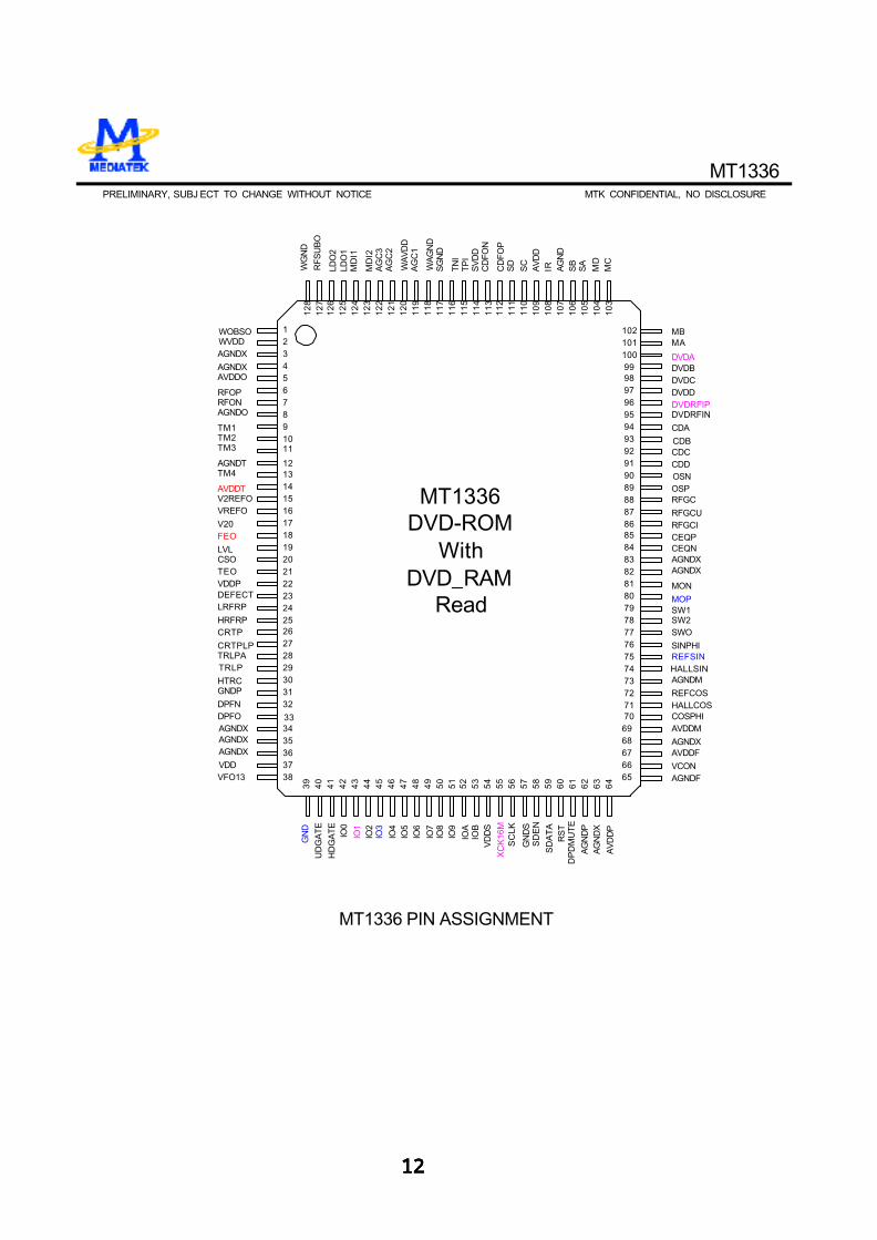
MT1336 PIN ASSIGNMENT
DP
DM
UT
E
AG
ND
PA
GN
DX
AV
DD
P
VCON
SA
SB
MC
MD
DVDBDVDA
DVDRFIP
DVDCDVDD
95949392919089888786858483828180797877767574737271706968676665
10110099989796
102
MT1336DVD-ROM
WithDVD_RAM
Read
AVDDO
RFOPRFONAGNDO
TM1TM2TM3
AGNDTTM4
AVDDT
IO4
SC
LK
AGNDX
SW1
SWO
GN
DS
CDB
CDA
DVDRFIN
AGNDF
MON
VFO13
AGNDXAGNDX
TRLPATRLP
HTRCGNDP
DPFNDPFO
IO1
AGNDX
VDD
IO5
IO7
IO8
IO9
FEO
IOB
SW2
IOA
1234567891011
1213
15161718192021222324
26272829303132
333435
3738
14
25
36
IO0
AVDDF
IO6
AGNDX
AVDDM
HALLCOSCOSPHI
REFCOS
AGNDMHALLSIN
UD
GA
TE
HD
GA
TE
39 40 41 42 43 45 46 47 49 50 51 52 5453 55 56 57 58 59 60 61 62 63 6444 48
IRAV
DD
SC
SDWG
ND
LDO
2
MD
I2
MD
I1
CD
FOP
SV
DD
TP
IT
NI
SG
ND
RFS
UB
O
WOBSOWVDD
LDO
1
WA
VD
DA
GC
1
AG
C2
AG
C3
WA
GN
D
121
120
119
118
117
116
115
114
113
112
111
110
109
108
107
106
105
104
103
127
126
125
124
123
122
128
AG
ND
RS
TS
DA
TA
SD
EN
V2REFO
LRFRP
HRFRPCRTP
CRTPLP
DEFECTVDDPTEOCSO
VREFO
V20
LVL
VD
DS
MB
RFGC
RFGCURFGCICEQPCEQNAGNDX
XC
K16
M
IO3
GN
D
REFSIN
MOP
CDCCDD
MA
OSNOSP
IO2
CD
FON
SINPHI
AGNDX
AGNDX
MT1336 PRELIMINARY, SUBJ ECT TO CHANGE WITHOUT NOTICE MTK CONFIDENTIAL, NO DISCLOSURE
MT1336 PIN DESCRIPTIONS
Pin Numbers Symbol Type Description
LQFP128
RF Flag Interface
23 DEFECT Digital Output Flag of bad data output status
RF SIO interface
56 SCLK Digital Input RF serial clock input
58 SDEN Digital Input RF serial data enable
59 SDATA Digital IO RF serial data IO
60 RST Digital input Reset (active high)
55 XCK16M Digital Input 16.9MHz for verification
RF SERVO interface
40 UDGATE Digital Input Con trol signal for DVD-RAM
41 IDGATE Digital Input Control signal for DVD-RAM
38 VFO13 Digital Input DVD -RAM Header signal
RF
100 DVDA Analog input AC coupled DVD RF signal input A
99 DVDB Analog Input AC coupled DVD RF signal input B
98 DVDC Analog Input AC coupled DVD RF signal input C
97 DVDD Analog Input AC coupled DVD RF signal input D
95 DVDRFIN Analog Input AC coupled DVD RF signal input RFIN
96 DVDRFIP Analog Input AC coupled DVD RF signal input RFIP
94 CDA Analog Input AC coupled CD RF signal input A
93 CDB Analog Input AC coupled CD RF signal input B
92 CDC Analog Input AC coupled CD RF signal input C
91 CDD Analog Input AC coupled CD RF signal input D
90 OSN Analog RF Offset cancellation capacitor connecting
89 OSP Analog RF Offset cancellation capacitor connecting
85 CEQP Analog RF Offset cancellation capacitor connecting
84 CEQN Analog RF Offset cancellation capacitor connecting
88 RFGC Analog RF AGC loop capacitor connecting for DVD -ROM
MT1336 PRELIMINARY, SUBJ ECT TO CHANGE WITHOUT NOTICE MTK CONFIDENTIAL, NO DISCLOSURE
87 RFGCU Analog RF AGC loop capacitor connecting for DVD -RAM
86 RFGCI Analog RF AGC loop capacitor connecting for DVD -RAM
101 MA Analog Input DC coupled DVD-RAM main-beam RF signal input A
102 MB Analog Input DC coupled DVD-RAM main-beam RF signal input B
103 MC Analog Input DC coupled DVD-RAM main-beam RF signal input C
104 MD Analog Input DC coupled DVD-RAM main-beam RF signal input D
105 SA Analog Input DC coupled DVD-RAM sub-beam RF signal input A
106 SB Analog Input DC coupled DVD-RAM sub-beam RF signal input B
110 SC Analog Input DC coupled DVD-RAM sub-beam RF signal input C
111 SD Analog Input DC coupled DVD-RAM sub-beam RF signal input D
108 IR Analog External current bias resistor (R=20K)
119 AGC1 Analog Wobble AGC loop1 capacitor
121 AGC2 Analog Wobble AGC loop2 capacitor
122 AGC3 Analog Wobble AGC loop3 capacitor
127 RFSUBO Analog output Header push-pull RF output signal
1 WOBSO Digital output Wobble signal output
6 RFOP Analog output RF positive output
7 RFON Analog output RF negative output
TRACKING ERROR
32 DPFN Analog DPD amplifier negative input
33 DPFO Analog DPD amplifier output
61 DPDMUTE Digital input DPD mute control input
116 TNI Analog Input 3 beam satellite PD signal negative input
115 TPI Analog Input 3 beam satellite PD signal positive input
21 TEO Analog Output Tracking error output
FOCUSING ERROR & RF LEVEL & CENTRAL SERVO SIGNAL
112 CDFOP Analog Input CD focusing error positive input
113 CDFON Analog Input CD focusing error negative input
18 FEO Analog Output Focusing error output
19 LVL Analog Output RF level output
20 CSO Analog output Central servo signal output
ALPC
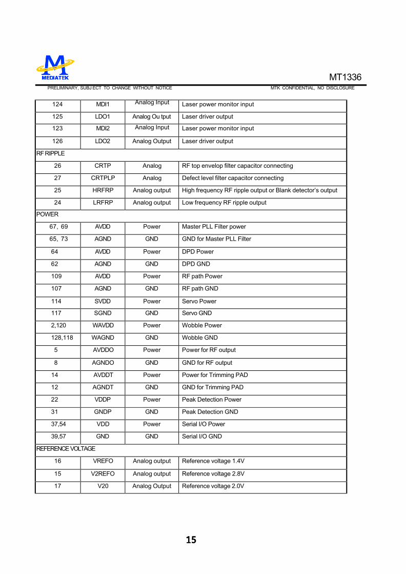
MT1336 PRELIMINARY, SUBJ ECT TO CHANGE WITHOUT NOTICE MTK CONFIDENTIAL, NO DISCLOSURE
124 MDI1 Analog Input Laser power monitor input
125 LDO1 Analog Ou tput Laser driver output
123 MDI2 Analog Input Laser power monitor input
126 LDO2 Analog Output Laser driver output
RF RIPPLE
26 CRTP Analog RF top envelop filter capacitor connecting
27 CRTPLP Analog Defect level filter capacitor connecting
25 HRFRP Analog output High frequency RF ripple output or Blank detector’s output
24 LRFRP Analog output Low frequency RF ripple output
POWER
67, 69 AVDD Power Master PLL Filter power
65, 73 AGND GND GND for Master PLL Filter
64 AVDD Power DPD Power
62 AGND GND DPD GND
109 AVDD Power RF path Power
107 AGND GND RF path GND
114 SVDD Power Servo Power
117 SGND GND Servo GND
2,120 WAVDD Power Wobble Power
128,118 WAGND GND Wobble GND
5 AVDDO Power Power for RF output
8 AGNDO GND GND for RF output
14 AVDDT Power Power for Trimming PAD
12 AGNDT GND GND for Trimming PAD
22 VDDP Power Peak Detection Power
31 GNDP GND Peak Detection GND
37,54 VDD Power Serial I/O Power
39,57 GND GND Serial I/O GND
REFERENCE VOLTAGE
16 VREFO Analog output Reference voltage 1.4V
15 V2REFO Analog output Reference voltage 2.8V
17 V20 Analog Output Reference voltage 2.0V
MT1336 PRELIMINARY, SUBJ ECT TO CHANGE WITHOUT NOTICE MTK CONFIDENTIAL, NO DISCLOSURE
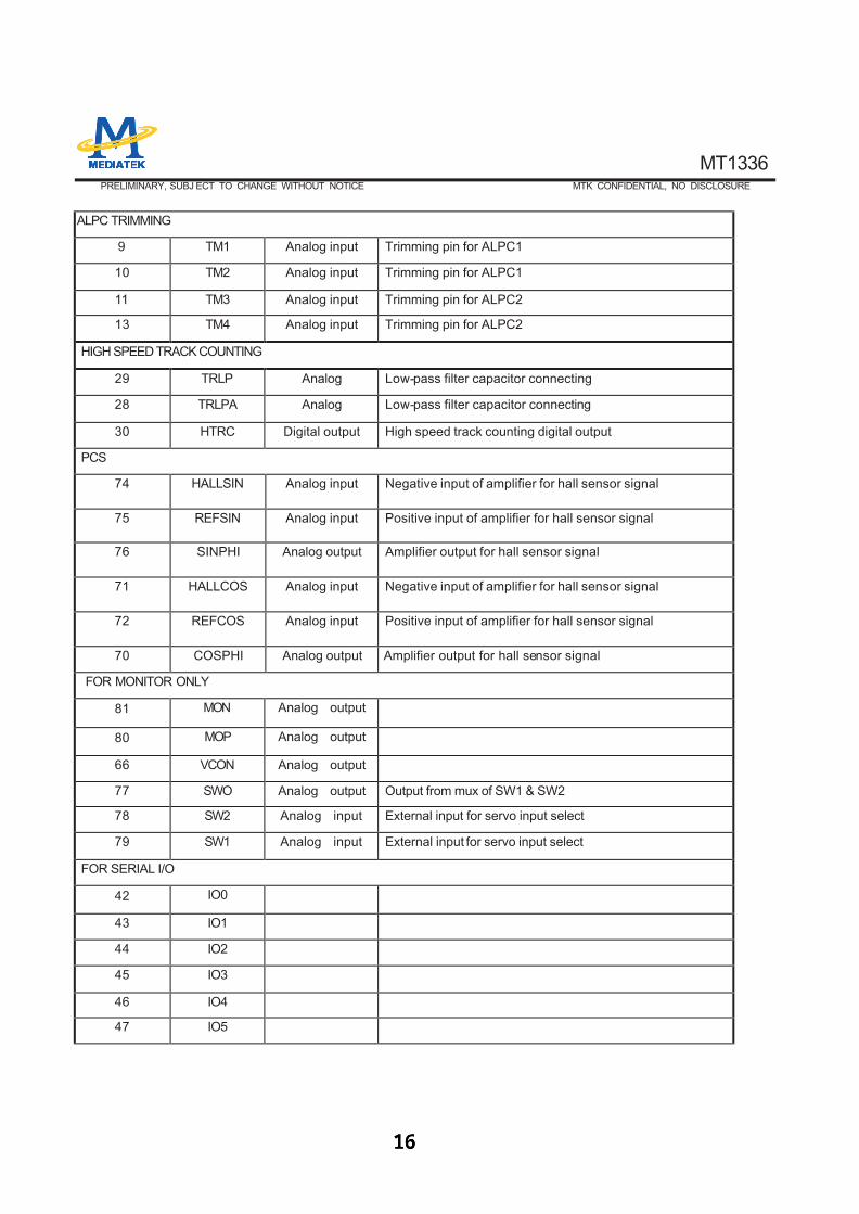
ALPC TRIMMING
9 TM1 Analog input Trimming pin for ALPC1
10 TM2 Analog input Trimming pin for ALPC1
11 TM3 Analog input Trimming pin for ALPC2
13 TM4 Analog input Trimming pin for ALPC2
HIGH SPEED TRACK COUNTING
29 TRLP Analog Low-pass filter capacitor connecting
28 TRLPA Analog Low-pass filter capacitor connecting
30 HTRC Digital output High speed track counting digital output
PCS
74 HALLSIN Analog input Negative input of amplifier for hall sensor signal
75 REFSIN Analog input Positive input of amplifier for hall sensor signal
76 SINPHI Analog output Amplifier output for hall sensor signal
71 HALLCOS Analog input Negative input of amplifier for hall sensor signal
72 REFCOS Analog input Positive input of amplifier for hall sensor signal
70 COSPHI Analog output Amplifier output for hall sensor signal
FOR MONITOR ONLY
81 MON Analog output
80 MOP Analog output
66 VCON Analog output
77 SWO Analog output Output from mux of SW1 & SW2
78 SW2 Analog input External input for servo input select
79 SW1 Analog input External input for servo input select
FOR SERIAL I/O
42 IO0
43 IO1
44 IO2
45 IO3
46 IO4
47 IO5
MT1336 PRELIMINARY, SUBJ ECT TO CHANGE WITHOUT NOTICE MTK CONFIDENTIAL, NO DISCLOSURE
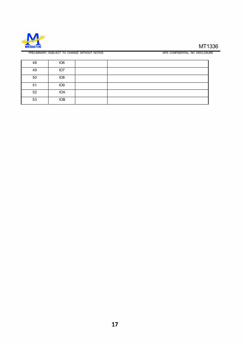
48 IO6
49 IO7
50 IO8
51 IO9
52 IOA
53 IOB
MT1379
Specifications are subject to change without notice Progressive Scan DVD Player Combo Chip
n Super Integration DVD player single chip
§ Servo controller and data channel processing § MPEG-1/MPEG-2/JPEG video decoding § Dolby AC-3/DTS/DVD-Audio audio decoding § Unified track buffer and A/V decoding buffer § Video processing for scaling and video quality
enhancement § OSD & Sub-picture decoding § Built-in clock generator § Built-in TV encoder § Built-in progressive video output § Video input port and audio/SPDIF input port
n Speed Performance on Servo and Decoding
§ DVD-ROM up to 8XS § CD-ROM up to 24XS § Built-in a frequency programmable clock to µP
and RSPC Decoder to optimize the performance over power
n Channel Data Processor
§ Provides interface with analog front-end processor
§ Analog data slicer for small jitter capability § Built-in high performance data PLL for chann el
data demodulation § EFM/EFM+ data demodulation § Enhanced channel data frame sync protection &
DVD-ROM sector sync protection
n Servo Control and Spindle Motor Control
§ Programmable frequency error gain and phase error gain of spindle PLL to control spindle motor on CLV and CAV mode
§ Provide a varipitch speed control for CLV and CAV mode
§ Built-in ADCs and DACs for digital servo control § Provide 2 general PWM
§ Tray control can be PWM output or digital output § Built-in DSP for digital servo control
n Host Micro controller
§ Built-in 8032 micro controller § Built-in internal 373 and 8-bit programmable
lower address port § 1024-bytes on-chip RAM § Up to 2M bytes FLASH-programming interface § Supports 5/3.3-Volt. FLASH interface § Supports power-down mode § Supports additional serial port
n DVD-ROM/CD-ROM Decoding Logic
§ Supports CD-ROM Mode 1, CD-ROM XA Mode 2 Form 1, CD-ROM XA Mode 2 Form 2, and CD-DA formats
§ High-speed ECC logic capable of correcting one error per each P-codeword or Q-codeword
§ Automatic sector Mode and Form detection § Automatic sector Header verification § 8-bit counter for decode completion check § Programmable descrambling and error
correction schemes § Automatically repeated error corrections § 8-bit C2 Pointer counter § Decoder Error Notification Interrupt that signals
various decoder errors § Provide error correction acceleration
n Buffer Memory Controller
§ Supports 16Mb/32Mb/64Mb/128Mb SDRAM § Supports 16-bit/32-bit SDRAM data bus interface § Build in a DRAM interface programmable clock to
optimize the DRAM performance § Provide the self-refresh mode SDRAM § Programmable DRAM access cycle and refresh
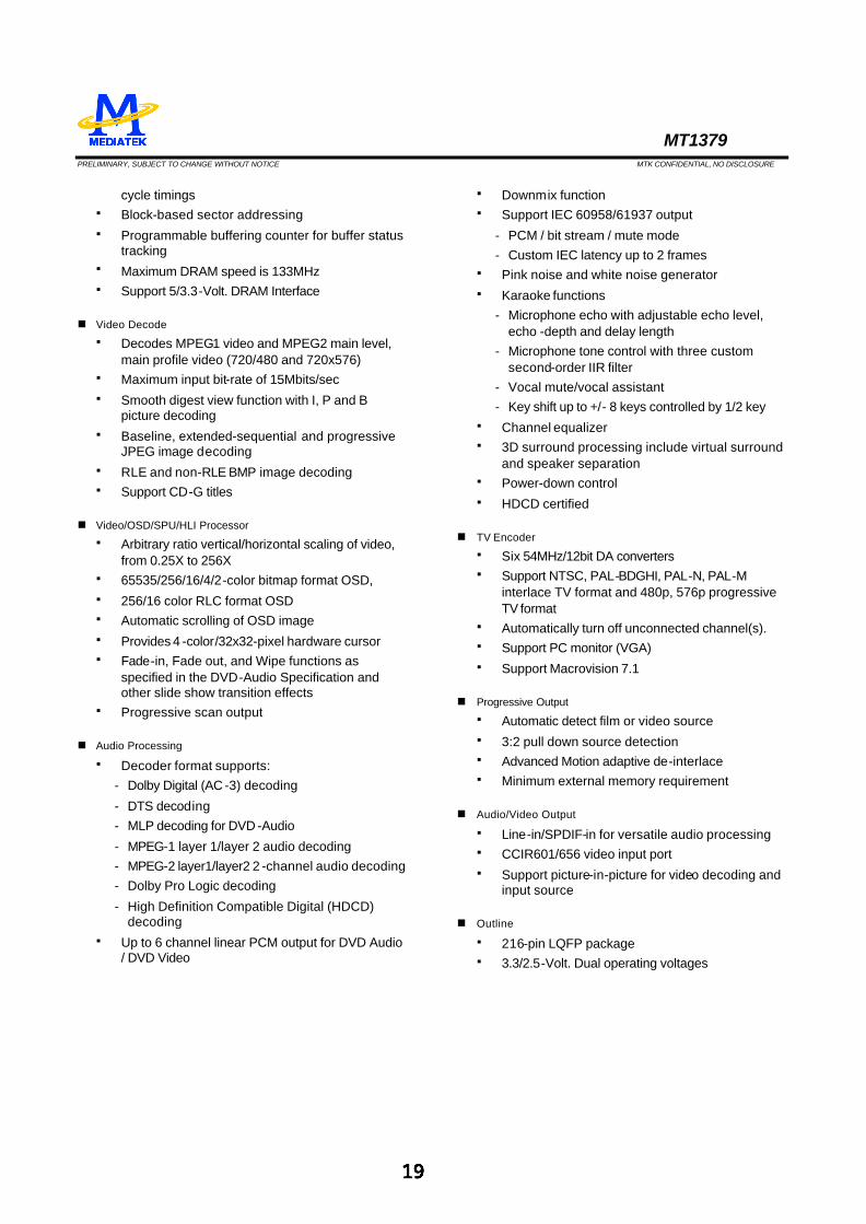
MT1379 PRELIMINARY, SUBJECT TO CHANGE WITHOUT NOTICE MTK CONFIDENTIAL, NO DISCLOSURE
cycle timings § Block-based sector addressing § Programmable buffering counter for buffer status
tracking § Maximum DRAM speed is 133MHz § Support 5/3.3-Volt. DRAM Interface
n Video Decode
§ Decodes MPEG1 video and MPEG2 main level, main profile video (720/480 and 720x576)
§ Maximum input bit-rate of 15Mbits/sec § Smooth digest view function with I, P and B
picture decoding § Baseline, extended-sequential and progressive
JPEG image decoding § RLE and non-RLE BMP image decoding § Support CD-G titles
n Video/OSD/SPU/HLI Processor
§ Arbitrary ratio vertical/horizontal scaling of video, from 0.25X to 256X
§ 65535/256/16/4/2-color bitmap format OSD, § 256/16 color RLC format OSD § Automatic scrolling of OSD image § Provides 4 -color/32x32-pixel hardware cursor § Fade-in, Fade out, and Wipe functions as
specified in the DVD-Audio Specification and other slide show transition effects
§ Progressive scan output
n Audio Processing
§ Decoder format supports: - Dolby Digital (AC -3) decoding
- DTS decoding - MLP decoding for DVD -Audio
- MPEG-1 layer 1/layer 2 audio decoding - MPEG-2 layer1/layer2 2 -channel audio decoding - Dolby Pro Logic decoding
- High Definition Compatible Digital (HDCD) decoding
§ Up to 6 channel linear PCM output for DVD Audio / DVD Video
§ Downmix function § Support IEC 60958/61937 output
- PCM / bit stream / mute mode - Custom IEC latency up to 2 frames
§ Pink noise and white noise generator § Karaoke functions
- Microphone echo with adjustable echo level, echo -depth and delay length
- Microphone tone control with three custom second-order IIR filter
- Vocal mute/vocal assistant - Key shift up to +/- 8 keys controlled by 1/2 key
§ Channel equalizer § 3D surround processing include virtual surround
and speaker separation § Power-down control § HDCD certified
n TV Encoder
§ Six 54MHz/12bit DA converters § Support NTSC, PAL-BDGHI, PAL-N, PAL-M
interlace TV format and 480p, 576p progressive TV format
§ Automatically turn off unconnected channel(s). § Support PC monitor (VGA) § Support Macrovision 7.1
n Progressive Output
§ Automatic detect film or video source § 3:2 pull down source detection § Advanced Motion adaptive de-interlace § Minimum external memory requirement
n Audio/Video Output
§ Line-in/SPDIF-in for versatile audio processing § CCIR601/656 video input port § Support picture-in-picture for video decoding and
input source
n Outline
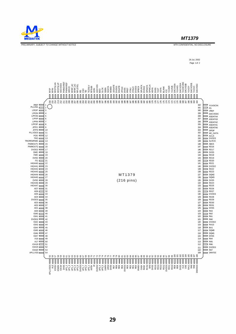
§ 216-pin LQFP package § 3.3/2.5-Volt. Dual operating voltages
MT1379 PRELIMINARY, SUBJECT TO CHANGE WITHOUT NOTICE MTK CONFIDENTIAL, NO DISCLOSURE
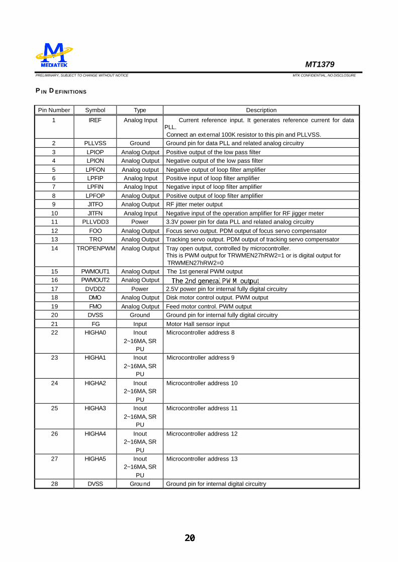
P IN D EFINITIONS
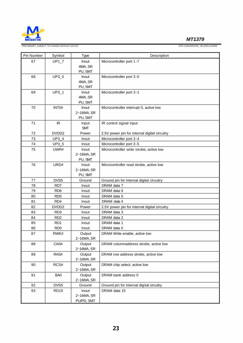
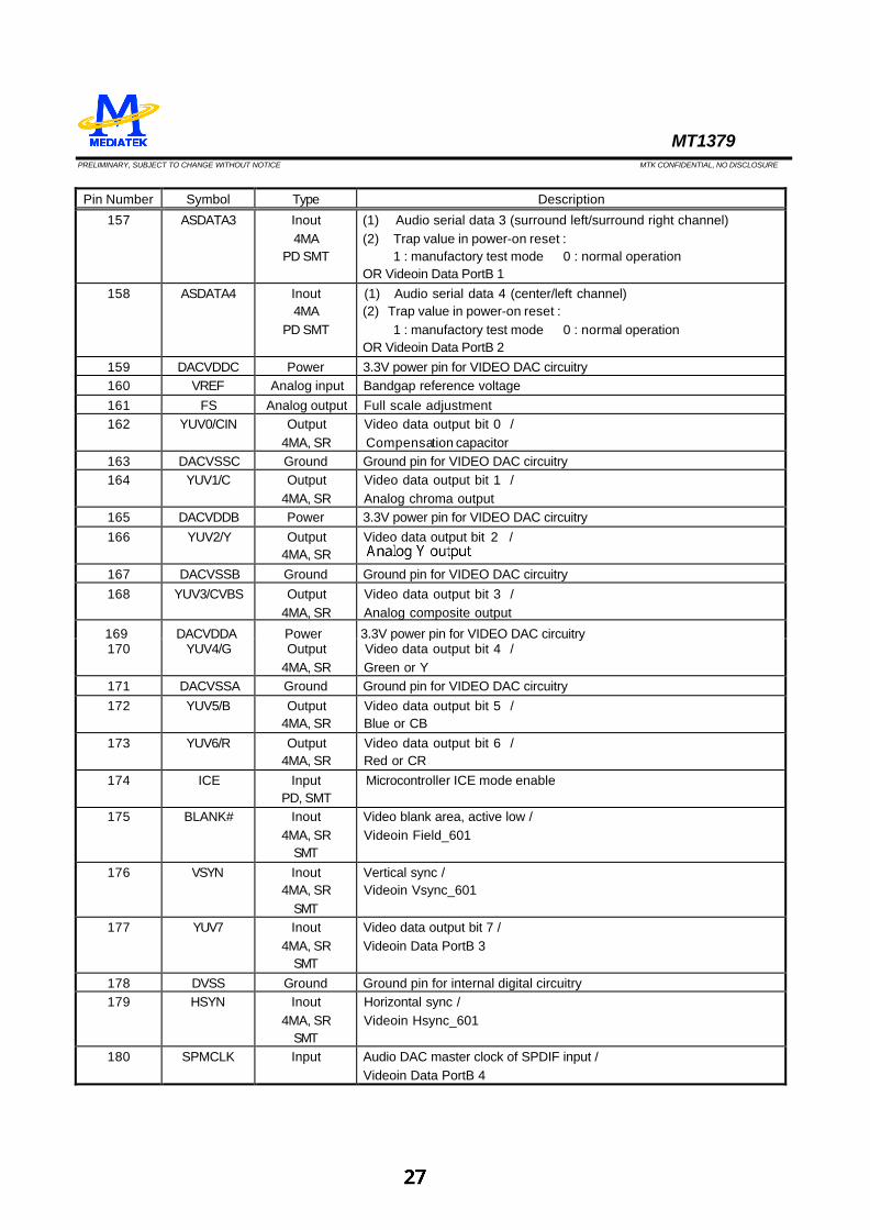
Pin Number Symbol Type Description
1 IREF Analog Input Current reference input. It generates reference current for data PLL. Connect an external 100K resistor to this pin and PLLVSS.
2 PLLVSS Ground Ground pin for data PLL and related analog circuitry 3 LPIOP Analog Output Positive output of the low pass filter 4 LPION Analog Output Negative output of the low pass filter 5 LPFON Analog output Negative output of loop filter amplifier 6 LPFIP Analog Input Positive input of loop filter amplifier 7 LPFIN Analog Input Negative input of loop filter amplifier 8 LPFOP Analog Output Positive output of loop filter amplifier 9 JITFO Analog Output RF jitter meter output 10 JITFN Analog Input Negative input of the operation amplifier for RF jigger meter 11 PLLVDD3 Power 3.3V power pin for data PLL and related analog circuitry 12 FOO Analog Output Focus servo output. PDM output of focus servo compensator 13 TRO Analog Output Tracking servo output. PDM output of tracking servo compensator 14 TROPENPWM Analog Output Tray open output, controlled by microcontroller.
This is PWM output for TRWMEN27hRW2=1 or is digital output for TRWMEN27hRW2=0
15 PWMOUT1 Analog Output The 1st general PWM output 16 PWMOUT2 Analog Output 17 DVDD2 Power 2.5V power pin for internal fully digital circuitry 18 DMO Analog Output Disk motor control output. PWM output 19 FMO Analog Output Feed motor control. PWM output 20 DVSS Ground Ground pin for internal fully digital circuitry 21 FG Input Motor Hall sensor input 22 HIGHA0 Inout
2~16MA, SR PU
Microcontroller address 8
23 HIGHA1 Inout 2~16MA, SR
PU
Microcontroller address 9
24 HIGHA2 Inout 2~16MA, SR
PU
Microcontroller address 10
25 HIGHA3 Inout 2~16MA, SR
PU
Microcontroller address 11
26 HIGHA4 Inout 2~16MA, SR
PU
Microcontroller address 12
27 HIGHA5 Inout 2~16MA, SR
PU
Microcontroller address 13
28 DVSS Ground Ground pin for internal digital circuitry
MT1379 PRELIMINARY, SUBJECT TO CHANGE WITHOUT NOTICE MTK CONFIDENTIAL, NO DISCLOSURE
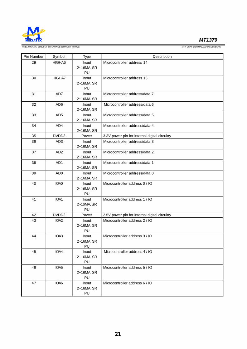
Pin Number Symbol Type Description
29 HIGHA6 Inout 2~16MA, SR
PU
Microcontroller address 14
30 HIGHA7 Inout 2~16MA, SR
PU
Microcontroller address 15
31 AD7 Inout 2~16MA, SR
Microcontroller address/data 7
32 AD6 Inout 2~16MA, SR
Microcontroller address/data 6
33 AD5 Inout 2~16MA, SR
Microcontroller address/data 5
34 AD4 Inout 2~16MA, SR
Microcontroller address/data 4
35 DVDD3 Power 3.3V power pin for internal digital circuitry 36 AD3 Inout
2~16MA, SR Microcontroller address/data 3
37 AD2 Inout 2~16MA, SR
Microcontroller address/data 2
38 AD1 Inout 2~16MA, SR
Microcontroller address/data 1
39 AD0 Inout 2~16MA, SR
Microcontroller address/data 0
40 IOA0 Inout 2~16MA, SR
PU
Microcontroller address 0 / IO
41 IOA1 Inout 2~16MA, SR
PU
Microcontroller address 1 / IO
42 DVDD2 Power 2.5V power pin for internal digital circuitry 43 IOA2 Inout
2~16MA, SR PU
Microcontroller address 2 / IO
44 IOA3 Inout 2~16MA, SR
PU
Microcontroller address 3 / IO
45 IOA4 Inout 2~16MA, SR
PU
Microcontroller address 4 / IO
46 IOA5 Inout 2~16MA, SR
PU
Microcontroller address 5 / IO
47 IOA6 Inout 2~16MA, SR
PU
Microcontroller address 6 / IO
MT1379 PRELIMINARY, SUBJECT TO CHANGE WITHOUT NOTICE MTK CONFIDENTIAL, NO DISCLOSURE
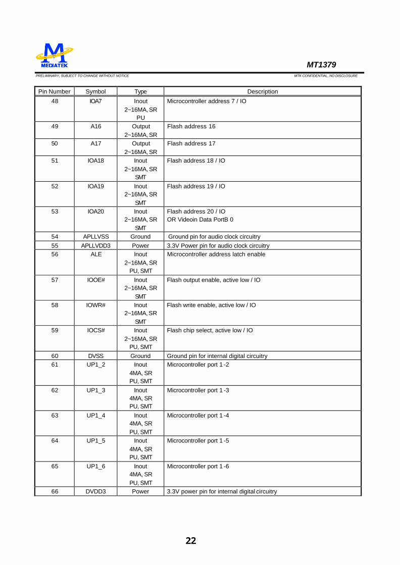
Pin Number Symbol Type Description
48 IOA7 Inout 2~16MA, SR
PU
Microcontroller address 7 / IO
49 A16 Output 2~16MA, SR
Flash address 16
50 A17 Output 2~16MA, SR
Flash address 17
51 IOA18 Inout 2~16MA, SR
SMT
Flash address 18 / IO
52 IOA19 Inout 2~16MA, SR
SMT
Flash address 19 / IO
53 IOA20 Inout 2~16MA, SR
SMT
Flash address 20 / IO OR Videoin Data PortB 0
54 APLLVSS Ground Ground pin for audio clock circuitry 55 APLLVDD3 Power 3.3V Power pin for audio clock circuitry 56 ALE Inout
2~16MA, SR PU, SMT
Microcontroller address latch enable
57 IOOE# Inout 2~16MA, SR
SMT
Flash output enable, active low / IO
58 IOWR# Inout 2~16MA, SR
SMT
Flash write enable, active low / IO
59 IOCS# Inout 2~16MA, SR
PU, SMT
Flash chip select, active low / IO
60 DVSS Ground Ground pin for internal digital circuitry 61 UP1_2 Inout
4MA, SR PU, SMT
Microcontroller port 1 -2
62 UP1_3 Inout 4MA, SR PU, SMT
Microcontroller port 1 -3
63 UP1_4 Inout 4MA, SR PU, SMT
Microcontroller port 1 -4
64 UP1_5 Inout 4MA, SR PU, SMT
Microcontroller port 1 -5
65 UP1_6 Inout 4MA, SR PU, SMT
Microcontroller port 1 -6
66 DVDD3 Power 3.3V power pin for internal digital circuitry
MT1379 PRELIMINARY, SUBJECT TO CHANGE WITHOUT NOTICE MTK CONFIDENTIAL, NO DISCLOSURE
Pin Number Symbol Type Description
67 UP1_7 Inout 4MA, SR PU, SMT
Microcontroller port 1 -7
68 UP3_0 Inout 4MA, SR PU, SMT
Microcontroller port 3 -0
69 UP3_1 Inout 4MA, SR PU, SMT
Microcontroller port 3 -1
70 INT0# Inout 2~16MA, SR
PU, SMT
Microcontroller interrupt 0, active low
71 IR Input SMT
IR control signal input
72 DVDD2 Power 2.5V power pin for internal digital circuitry 73 UP3_4 Inout Microcontroller port 3 -4 74 UP3_5 Inout Microcontroller port 3 -5 75 UWR# Inout
2~16MA, SR PU, SMT
Microcontroller write strobe, active low
76 URD# Inout 2~16MA, SR
PU, SMT
Microcontroller read strobe, active low
77 DVSS Ground Ground pin for internal digital circuitry 78 RD7 Inout DRAM data 7 79 RD6 Inout DRAM data 6 80 RD5 Inout DRAM data 5 81 RD4 Inout DRAM data 4 82 DVDD2 Power 2.5V power pin for internal digital circuitry 83 RD3 Inout DRAM data 3 84 RD2 Inout DRAM data 2 85 RD1 Inout DRAM data 1 86 RD0 Inout DRAM data 0 87 RWE# Output
2~16MA, SR DRAM Write enable, active low
88 CAS# Output 2~16MA, SR
DRAM columnaddress strobe, active low
89 RAS# Output 2~16MA, SR
DRAM row address strobe, active low
90 RCS# Output 2~16MA, SR
DRAM chip select, active low
91 BA0 Output 2~16MA, SR
DRAM bank address 0
92 DVSS Ground Ground pin for internal digital circuitry 93 RD15 Inout
2~16MA, SR PU/PD, SMT
DRAM data 15
MT1379 PRELIMINARY, SUBJECT TO CHANGE WITHOUT NOTICE MTK CONFIDENTIAL, NO DISCLOSURE
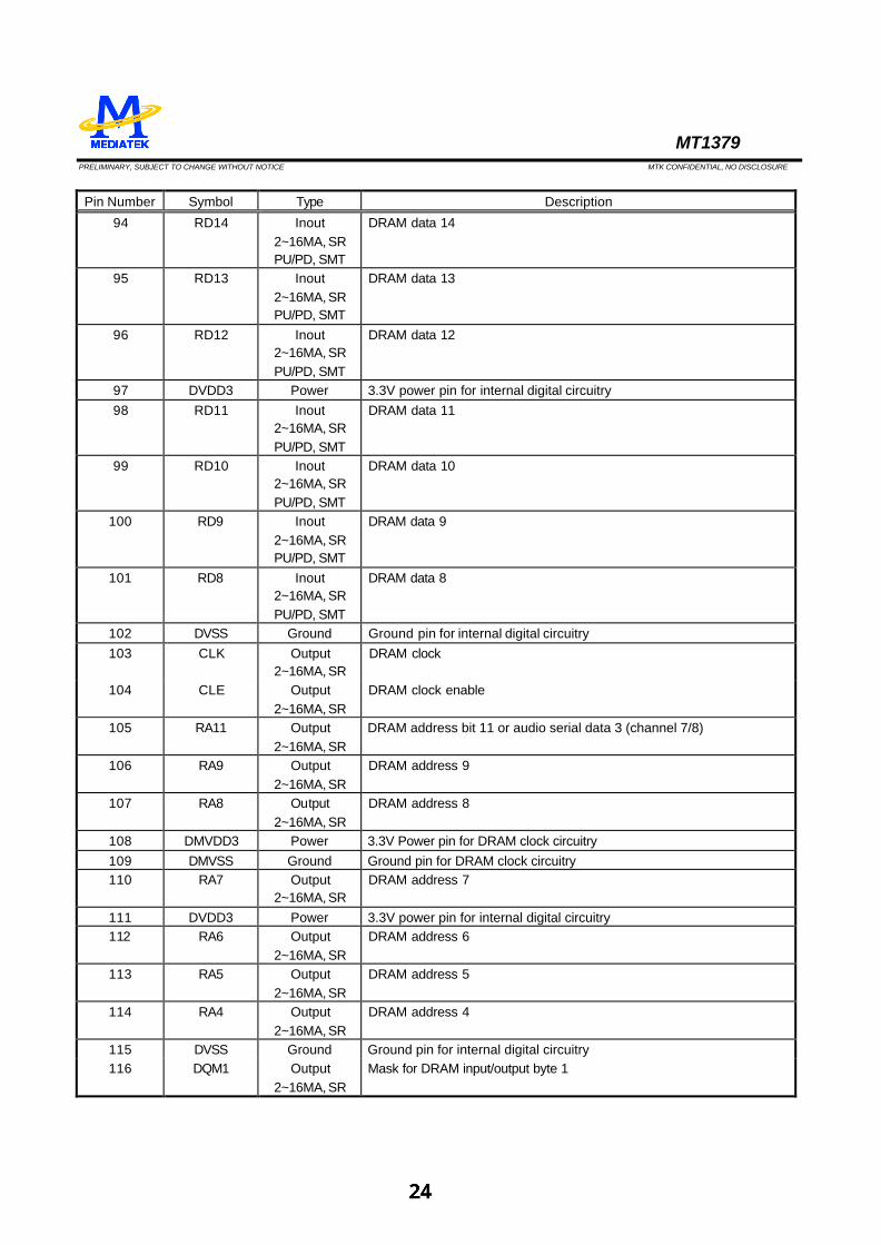
Pin Number Symbol Type Description
94 RD14 Inout 2~16MA, SR PU/PD, SMT
DRAM data 14
95 RD13 Inout 2~16MA, SR PU/PD, SMT
DRAM data 13
96 RD12 Inout 2~16MA, SR PU/PD, SMT
DRAM data 12
97 DVDD3 Power 3.3V power pin for internal digital circuitry 98 RD11 Inout
2~16MA, SR PU/PD, SMT
DRAM data 11
99 RD10 Inout 2~16MA, SR PU/PD, SMT
DRAM data 10
100 RD9 Inout 2~16MA, SR PU/PD, SMT
DRAM data 9
101 RD8 Inout 2~16MA, SR PU/PD, SMT
DRAM data 8
102 DVSS Ground Ground pin for internal digital circuitry 103 CLK Output
2~16MA, SR DRAM clock
104 CLE Output 2~16MA, SR
DRAM clock enable
105 RA11 Output 2~16MA, SR
DRAM address bit 11 or audio serial data 3 (channel 7/8)
106 RA9 Output 2~16MA, SR
DRAM address 9
107 RA8 Output 2~16MA, SR
DRAM address 8
108 DMVDD3 Power 3.3V Power pin for DRAM clock circuitry 109 DMVSS Ground Ground pin for DRAM clock circuitry 110 RA7 Output
2~16MA, SR DRAM address 7
111 DVDD3 Power 3.3V power pin for internal digital circuitry 112 RA6 Output
2~16MA, SR DRAM address 6
113 RA5 Output 2~16MA, SR
DRAM address 5
114 RA4 Output 2~16MA, SR
DRAM address 4
115 DVSS Ground Ground pin for internal digital circuitry 116 DQM1 Output
2~16MA, SR Mask for DRAM input/output byte 1
MT1379 PRELIMINARY, SUBJECT TO CHANGE WITHOUT NOTICE MTK CONFIDENTIAL, NO DISCLOSURE
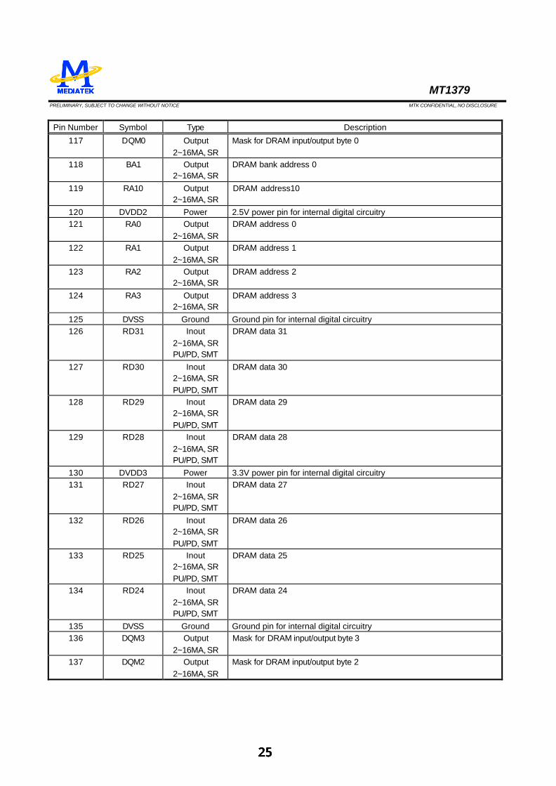
Pin Number Symbol Type Description
117 DQM0 Output 2~16MA, SR
Mask for DRAM input/output byte 0
118 BA1 Output 2~16MA, SR
DRAM bank address 0
119 RA10 Output 2~16MA, SR
DRAM address10
120 DVDD2 Power 2.5V power pin for internal digital circuitry 121 RA0 Output
2~16MA, SR DRAM address 0
122 RA1 Output 2~16MA, SR
DRAM address 1
123 RA2 Output 2~16MA, SR
DRAM address 2
124 RA3 Output 2~16MA, SR
DRAM address 3
125 DVSS Ground Ground pin for internal digital circuitry 126 RD31 Inout
2~16MA, SR PU/PD, SMT
DRAM data 31
127 RD30 Inout 2~16MA, SR PU/PD, SMT
DRAM data 30
128 RD29 Inout 2~16MA, SR PU/PD, SMT
DRAM data 29
129 RD28 Inout 2~16MA, SR PU/PD, SMT
DRAM data 28
130 DVDD3 Power 3.3V power pin for internal digital circuitry 131 RD27 Inout
2~16MA, SR PU/PD, SMT
DRAM data 27
132 RD26 Inout 2~16MA, SR PU/PD, SMT
DRAM data 26
133 RD25 Inout 2~16MA, SR PU/PD, SMT
DRAM data 25
134 RD24 Inout 2~16MA, SR PU/PD, SMT
DRAM data 24
135 DVSS Ground Ground pin for internal digital circuitry 136 DQM3 Output
2~16MA, SR Mask for DRAM input/output byte 3
137 DQM2 Output 2~16MA, SR
Mask for DRAM input/output byte 2
MT1379 PRELIMINARY, SUBJECT TO CHANGE WITHOUT NOTICE MTK CONFIDENTIAL, NO DISCLOSURE
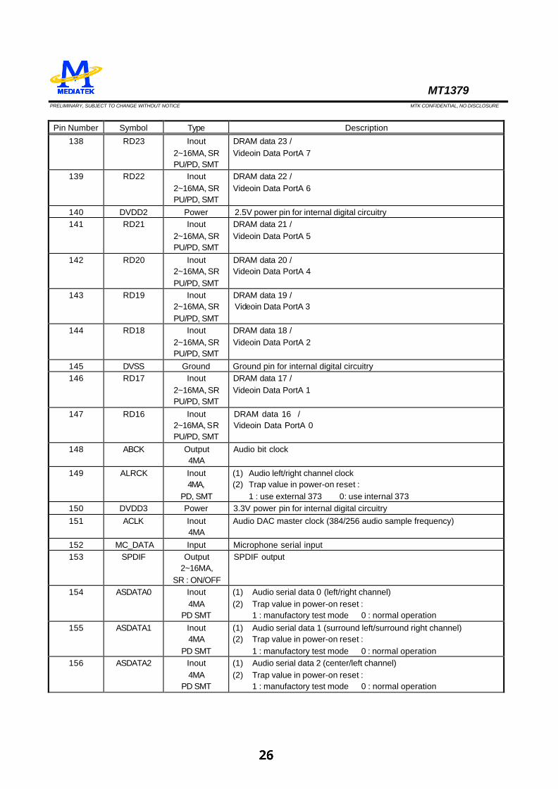
Pin Number Symbol Type Description
138 RD23 Inout 2~16MA, SR PU/PD, SMT
DRAM data 23 / Videoin Data PortA 7
139 RD22 Inout 2~16MA, SR PU/PD, SMT
DRAM data 22 / Videoin Data PortA 6
140 DVDD2 Power 2.5V power pin for internal digital circuitry 141 RD21 Inout
2~16MA, SR PU/PD, SMT
DRAM data 21 / Videoin Data PortA 5
142 RD20 Inout 2~16MA, SR PU/PD, SMT
DRAM data 20 / Videoin Data PortA 4
143 RD19 Inout 2~16MA, SR PU/PD, SMT
DRAM data 19 / Videoin Data PortA 3
144 RD18 Inout 2~16MA, SR PU/PD, SMT
DRAM data 18 / Videoin Data PortA 2
145 DVSS Ground Ground pin for internal digital circuitry 146 RD17 Inout
2~16MA, SR PU/PD, SMT
DRAM data 17 / Videoin Data PortA 1
147 RD16 Inout 2~16MA, SR PU/PD, SMT
DRAM data 16 / Videoin Data PortA 0
148 ABCK Output 4MA
Audio bit clock
149 ALRCK Inout 4MA,
PD, SMT
(1) Audio left/right channel clock (2) Trap value in power-on reset :
1 : use external 373 0: use internal 373 150 DVDD3 Power 3.3V power pin for internal digital circuitry 151 ACLK Inout
4MA Audio DAC master clock (384/256 audio sample frequency)
152 MC_DATA Input Microphone serial input 153 SPDIF Output
2~16MA, SR : ON/OFF
SPDIF output
154 ASDATA0 Inout 4MA
PD SMT
(1) Audio serial data 0 (left/right channel) (2) Trap value in power-on reset :
1 : manufactory test mode 0 : normal operation 155 ASDATA1 Inout
4MA PD SMT
(1) Audio serial data 1 (surround left/surround right channel) (2) Trap value in power-on reset : 1 : manufactory test mode 0 : normal operation
156 ASDATA2 Inout 4MA
PD SMT
(1) Audio serial data 2 (center/left channel) (2) Trap value in power-on reset : 1 : manufactory test mode 0 : normal operation
MT1379 PRELIMINARY, SUBJECT TO CHANGE WITHOUT NOTICE MTK CONFIDENTIAL, NO DISCLOSURE
Pin Number Symbol Type Description
157 ASDATA3 Inout 4MA
PD SMT
(1) Audio serial data 3 (surround left/surround right channel) (2) Trap value in power-on reset : 1 : manufactory test mode 0 : normal operation OR Videoin Data PortB 1
158 ASDATA4 Inout 4MA
PD SMT
(1) Audio serial data 4 (center/left channel) (2) Trap value in power-on reset : 1 : manufactory test mode 0 : normal operation OR Videoin Data PortB 2
159 DACVDDC Power 3.3V power pin for VIDEO DAC circuitry 160 VREF Analog input Bandgap reference voltage 161 FS Analog output Full scale adjustment 162 YUV0/CIN Output
4MA, SR Video data output bit 0 / Compensation capacitor
163 DACVSSC Ground Ground pin for VIDEO DAC circuitry 164 YUV1/C Output
4MA, SR Video data output bit 1 / Analog chroma output
165 DACVDDB Power 3.3V power pin for VIDEO DAC circuitry 166 YUV2/Y Output
4MA, SR Video data output bit 2 /
167 DACVSSB Ground Ground pin for VIDEO DAC circuitry 168 YUV3/CVBS Output
4MA, SR Video data output bit 3 / Analog composite output
169 DACVDDA Power 3.3V power pin for VIDEO DAC circuitry 170 YUV4/G Output
4MA, SR Video data output bit 4 / Green or Y
171 DACVSSA Ground Ground pin for VIDEO DAC circuitry 172 YUV5/B Output
4MA, SR Video data output bit 5 / Blue or CB
173 YUV6/R Output 4MA, SR
Video data output bit 6 / Red or CR
174 ICE
Input PD, SMT
Microcontroller ICE mode enable
175 BLANK# Inout 4MA, SR
SMT
Video blank area, active low / Videoin Field_601
176 VSYN Inout 4MA, SR
SMT
Vertical sync / Videoin Vsync_601
177 YUV7 Inout 4MA, SR
SMT
Video data output bit 7 / Videoin Data PortB 3
178 DVSS Ground Ground pin for internal digital circuitry 179 HSYN Inout
4MA, SR SMT
Horizontal sync / Videoin Hsync_601
180 SPMCLK Input Audio DAC master clock of SPDIF input / Videoin Data PortB 4
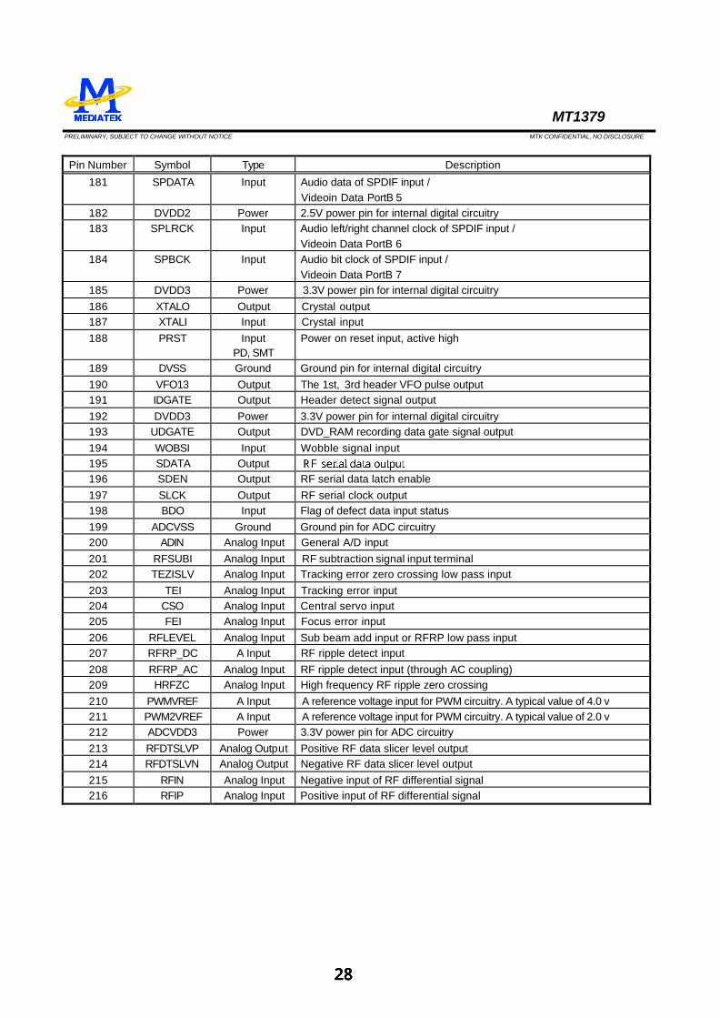
MT1379 PRELIMINARY, SUBJECT TO CHANGE WITHOUT NOTICE MTK CONFIDENTIAL, NO DISCLOSURE
Pin Number Symbol Type Description
181 SPDATA Input Audio data of SPDIF input / Videoin Data PortB 5
182 DVDD2 Power 2.5V power pin for internal digital circuitry 183 SPLRCK Input Audio left/right channel clock of SPDIF input /
Videoin Data PortB 6 184 SPBCK Input Audio bit clock of SPDIF input /
Videoin Data PortB 7 185 DVDD3 Power 3.3V power pin for internal digital circuitry 186 XTALO Output Crystal output 187 XTALI Input Crystal input 188 PRST Input
PD, SMT Power on reset input, active high
189 DVSS Ground Ground pin for internal digital circuitry 190 VFO13 Output The 1st, 3rd header VFO pulse output 191 IDGATE Output Header detect signal output 192 DVDD3 Power 3.3V power pin for internal digital circuitry 193 UDGATE Output DVD_RAM recording data gate signal output 194 WOBSI Input Wobble signal input 195 SDATA Output 196 SDEN Output RF serial data latch enable 197 SLCK Output RF serial clock output 198 BDO Input Flag of defect data input status 199 ADCVSS Ground Ground pin for ADC circuitry 200 ADIN Analog Input General A/D input 201 RFSUBI Analog Input RF subtraction signal input terminal 202 TEZISLV Analog Input Tracking error zero crossing low pass input 203 TEI Analog Input Tracking error input 204 CSO Analog Input Central servo input 205 FEI Analog Input Focus error input 206 RFLEVEL Analog Input Sub beam add input or RFRP low pass input 207 RFRP_DC A Input RF ripple detect input 208 RFRP_AC Analog Input RF ripple detect input (through AC coupling) 209 HRFZC Analog Input High frequency RF ripple zero crossing 210 PWMVREF A Input A reference voltage input for PWM circuitry. A typical value of 4.0 v 211 PWM2VREF A Input A reference voltage input for PWM circuitry. A typical value of 2.0 v 212 ADCVDD3 Power 3.3V power pin for ADC circuitry 213 RFDTSLVP Analog Output Positive RF data slicer level output 214 RFDTSLVN Analog Output Negative RF data slicer level output 215 RFIN Analog Input Negative input of RF differential signal 216 RFIP Analog Input Positive input of RF differential signal
MT1379 PRELIMINARY, SUBJECT TO CHANGE WITHOUT NOTICE MTK CONFIDENTIAL, NO DISCLOSURE
26 Jul, 2002
Page 1 of 2
M T 1 3 7 9
(216 p ins )
111
RA4
110109
RA7
RA6RA5
150149
147146145
148
143142141
144
139138137
140
135134133
136
131130129
132
127126125
128
123122121
124
119118117
120
115114113
116
112
RD26
DQM1
RA0
DQM0BA1
RD30
RA10
RA1RA2RA3
RD31
DVDD2
RD29RD28
RD27DVDD3
RD21
RD25RD24
DQM2
RD22RD23
DQM3
RD18RD19RD20
RD17
DVDD2
ABCKRD16
ASDATA2ASDATA1
DVSS
ALRCK
ASDATA0
155154153
156
151152
78
101112
9
141516
13
181920
17
222324
21
262728
25
303132
29
343536
33
383940
37
424344
41
4645
DVSS
IOA1IOA0
IOA3IOA4
IOA2
DMO
FG
DVDD2
FMODVSS
TROFOO
LPFIN
PLLVDD3JITFNJITFO
LPFOP
PLLVSS
4748
505152
49
IOA5IOA6IOA7
APLLVSS
234
1
65
IREF
LPIONLPIOP
LPFIPLPFON
RFR
P_AC
163
164
165
166
167
168
169
170
171
172
173
174
175
176
177
178
179
180
181
182
183
184
185
186
187
188
189
190
191
192
193
194
195
196
197
198
199
200
201
202
YU
V4/
G
YU
V6/
R
YUV7
RFR
P_D
C
FEI
RFL
EV
EL
HR
FZC
PRST
VFO
13
DV
DD
3
DVS
S
IDG
ATE
SD
ATA
DV
DD
3
CSO
PW
M2V
RE
F
BDO
UD
GAT
E
SDEN
WO
BSI
SLC
K
TEI
PW
MV
RE
F
AD
INR
FSU
BITE
ZIS
LV
DV
DD
2
SP
BC
K
DA
CV
SS
B
DA
CV
DD
A
203
204
205
206
207
208
RFI
NR
FDTS
LVN
RFI
P
RFD
TSLV
P
98979695949392919089888786858483828180797877767574737271706968676665646362616059
DV
DD
3
UP3
_5
IOO
E#
INT0
#
UP1
_7
UP3
_4
UP3
_0
RD
5
DVS
S
RD
4
RD
6
RD
3R
D2
RD
1R
D0
RW
E#
CAS
#R
AS#
RC
S#
RD
14R
D13
RD
12
BA
0
RD
15
RD
10R
D9
RD
11
RD
7
DVS
S
58575655 104
103
102
101
100
99
DV
DD
3
DVDD3
DVSS
ACLK
DVS
S
DVDD2
DVS
S
DA
CV
DD
B
DAC
VSSC
HSY
N
VSYN
BLA
NK
DVSS
DVDD3
DV
DD
2
DV
DD
2
IOC
S#
AD3
AD1AD0
AD2
HIGHA0
HIGHA3
HIGHA1HIGHA2
HIGHA5
AD6AD5
AD7
AD4
HIGHA4
HIGHA6HIGHA7
A16A17
IOA18
IOW
R#
UP1
_2U
P1_3
UP1
_4U
P1_5
UP1
_6
ICE
UP3
_1
UR
D#IR
UW
R#
ALE
DVDD3TROPENPWM
PWMOUT2
IOA19
RD
8
DVSS
5354
108
107
106
105
161160159
162
157158
209
210
211
212
213
214
215
216
PWMOUT1
AP
LLV
DD
3
DM
VD
D3
DMVSS
CKE
RA
11
CLK
DVS
S
RA9
VREFDACVDDC
FSYUV0/CIN
ASDATA3ASDATA4
XTAL
IXT
ALO
YU
V2/
Y
YU
V1/
C
YUV3
/CVB
S
SP
LRC
K
SP
DA
TA
IOA20
RA8
SPDIFMC_DATA
SP
MC
LK
DA
CV
SS
AY
UV
5/B
AD
CV
SS
AD
CV
DD
3
MT1379 PRELIMINARY, SUBJECT TO CHANGE WITHOUT NOTICE MTK CONFIDENTIAL, NO DISCLOSURE
F UNCTIONAL B LOCK
ServoD S P
ServoIO
A n a l o gF ron t end
D P U C h a n n e lD e c o d e
M i c r o p h o n eInpu t
Aud ioO u t p u t
Aud ioP r o c e s s o r
D R A MIn te r face
V i d e oD e c o d e r
S y s t e mP a r s e r
V i d e oO u t p u t
P l a y b a c kCont ro l l e r
S y s t e mCont ro l l e r
C S S /C P P M
D R A MF l a s h
I R /VFD
D V D m o d u l e
D e b u gPor t
S P D I F
Sp ind leCon t ro l l e r
T V e n c o d e r
A u d i o D A CMIC
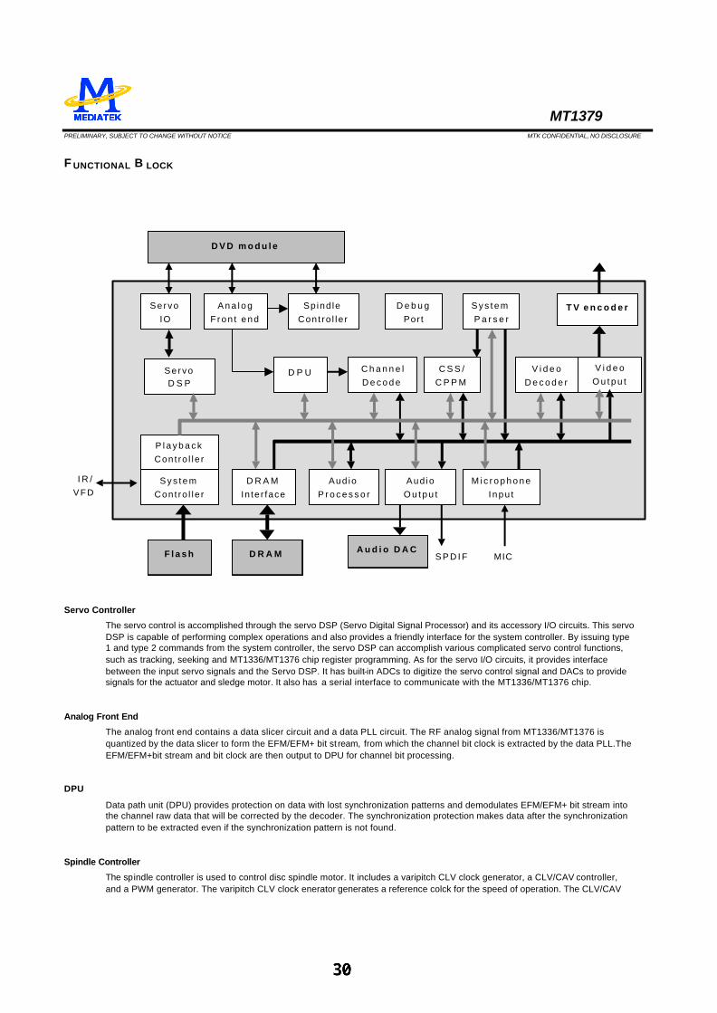
Servo Controller
The servo control is accomplished through the servo DSP (Servo Digital Signal Processor) and its accessory I/O circuits. This servo DSP is capable of performing complex operations and also provides a friendly interface for the system controller. By issuing type 1 and type 2 commands from the system controller, the servo DSP can accomplish various complicated servo control functions, such as tracking, seeking and MT1336/MT1376 chip register programming. As for the servo I/O circuits, it provides interface between the input servo signals and the Servo DSP. It has built-in ADCs to digitize the servo control signal and DACs to provide signals for the actuator and sledge motor. It also has a serial interface to communicate with the MT1336/MT1376 chip.
Analog Front End
The analog front end contains a data slicer circuit and a data PLL circuit. The RF analog signal from MT1336/MT1376 is quantized by the data slicer to form the EFM/EFM+ bit st ream, from which the channel bit clock is extracted by the data PLL.The EFM/EFM+bit stream and bit clock are then output to DPU for channel bit processing.
DPU
Data path unit (DPU) provides protection on data with lost synchronization patterns and demodulates EFM/EFM+ bit stream into the channel raw data that will be corrected by the decoder. The synchronization protection makes data after the synchronization pattern to be extracted even if the synchronization pattern is not found.
Spindle Controller
The spindle controller is used to control disc spindle motor. It includes a varipitch CLV clock generator, a CLV/CAV controller, and a PWM generator. The varipitch CLV clock enerator generates a reference colck for the speed of operation. The CLV/CAV
MT1379 PRELIMINARY, SUBJECT TO CHANGE WITHOUT NOTICE MTK CONFIDENTIAL, NO DISCLOSURE
controller changes the mode and speed of operation according to servo register setting. The PWM generator generates pulse -width-modulated signal to drive disc spindle motor driver.
CSS/CPPM
The CSS/CPPM module provides functions necessary for decoding discs conforming to CSS/CPPM specification.
System Parser
The system parser is used to help the system controller to decode DVD/SVCD/VCD bitstream just after the channel decoder performing error correction. Acting as a DMA master, it moves bitstream data from RSPC buffer to video, audio, or sub-picture buffer according to system controller request. It also decrypts the scramble data of the CSS/CPPM sectors. Another function of system parser is providing system controller/DSP a DRAM memory copy controller to enhance system controller/DSP performance.
Video Decoder
The primary function of MT1379 is to support MPEG1 and MPEG2 video decoding. The video decode engine comprises of variable length decoder (VLD), inverse transformer (IT), motion compensator (MC), and block reconst ructor (BR). The video decode engine decodes the variable length encoded symbols in MPEG bitstream and performs inverse scan, inverse quantization, mismatch control and inverse discrete cosine transform onto the variable length decoded data. The motion compensator fetches prediction data from reference picture buffer according to motion vectors and motion prediciton mode for P and B pictures. Finally, the block reconstructor combines both the results of inverse transformer and motion compensator to derive the reconstructed image macroblock and write back to picture buffer. The video decode engine can also support JPEG and BMP file decoding by common image compression hardware kernels.
Video Output
The Video Output unit contains Video Processor, SPU, OSD, Cursor, TV encoder units, it performs § Reading decoded video from DRAM buffer § Scaling the image § Gamma/Brightness/Hue/Saturation adjustment and edge enhancement § Reading and decoding SPU and OSD data from DRAM buffer § Generating hardware cursor image § Merging the video data, SPU, OSD and cursor Video Processor
The Video Processor unit controls the transfer of video data stored in the DRAM to an internal or external TV encoder. It uses FIFOs to buffer outgoing luminance and chrominance data, and performs YUV420 to YUV422 conversion and arbitrary vertical/horizontal decimation/interpolation, from 1/4x to 256x. With this arbitrary ratio scaling capability, the Video Processor can perform arbitrary image conversion, such as PAL to NTSC, NTSC to PAL, MPEG1 to MPEG2, Letterbox, Pan-Scan conversion or zoom in, zoom out. It is also capible of interlace to progressive conversion. The Video Processor unit performs the following functions: § Requests and receives the decoded picture data from the picture buffer in external DRAM for display § Resample vertical data to create 4:2:2 sample format § Optionally performs vertical/horizontal resampling of both luminance and chrominance data § Performs optional Gamma correction, luminance/chrominance adjustment, and edge enhancement The V ideo Processor unit contains two 2-tap vertical filters for luminance and chrominance . These filters are used to interpolate and reposition luminance and chrominance line to improve picture quality. These filters are capble of generating up to eight, unique subline value between two consecutive scan lines. The generation of lines depends on the ratio between the height of the source image and the target image. In applications where DRAM bandwidth are critical the filters can be configured as simple line-repeating to reduce the DRAM bandwidth required. The Video Processor unit integrates two separate horizontal postprocessing filter, a simple 2-tap linear horizontal filter and an 8-tap programmable filter. These filters are provided for scaling images horizontally along the scan line. These two filters is capable of generating up to eight, unique subpixel values between two consecutive pixels on a scan line. The generation of pixels depends on the ratio between the width of the source image and the target image.
SPU
MT1379 PRELIMINARY, SUBJECT TO CHANGE WITHOUT NOTICE MTK CONFIDENTIAL, NO DISCLOSURE
This is a hardware sub-picture decoder. It decodes the compressed SPU image bitstream and CHG_COLCON commands according to SPU header information previously decoded by system controller. The SPU module also allows two SPU objects to be displayed at the same time. SPU image is blended with main video stream.
OSD
The OSD module can operate with 2/4/16/256 -color bitmap format (1/2/4/8 bits), and 16/256 color RLC format, all have 16 levels of transparency. In addition, it accepts an special WARP mode, which inserts one programmable RLC code in the bitmap to reduce the image size stored in DRAM. It also features automatic shadow/outline generation in 2-color mode, 2 Hilight areas, 1 ChangeColor area and 1 OSDVoid area. One OSD area can occupy the full or a partial screen, or multiple OSDs can occur in a screen at the same time, only if they don't occupy the same horizontal line. The output image is blended with the video-SPU mixed stream.
Cursor
A hardware cursor generator is integrated in Video Ou tput Unit. The cursor image is a 32x32 4-color bitmap image, each colors are programmable. Cursor can be enlarged by 2 in both vertical and horizontal directions. Cursor image is multiplexed with video-SPU-OSD mixed stream.
Audio Interface
Audio interface consists of Audio Output Interface and Microphone Input Interface. Audio Output Interface
The MT1379 can support up to 8 channel audio outputs. The output formats can be 16, 24, or 32-bit frames. Left alignment, right alignment, or I 2S formats are all supported. With built-in PLL, MT1379 can provide the audio clock (ACLK) for external audio DAC at 384Fs, where Fs is usually 32KHz, 44.1KHz, 48KHz, 96KHz, or 192KHz. ACLK can also be programmed to be from outside MT1379. When ACLK is input to MT1379, the frequency could be 128*n Fs, where n is from 1 to 7. Audio raw (encoded) data or cooked (decoded) data can be output on a single line using S/PDIF interface. The output slew rate and driving force of this pad are programmable.
Microphone Input Interface The MT1379 provides a microphone input interface. Two independent microphones’ data could be input to the MT1379. There are two independent digital volume control for these two input channels. The input data formats can also be left alignment, right alignment, or I2S formats.
System Controller
MT1379 uses an embedded Turbo-8032 as System Controller and provide ICE interface to increase the feasibility of F/W development. Also, MT1379 includes an build-in internal 373 to latch lower byte address from 8032 Port 0 and provide a glue-logic free solution. MT1379 supports up to 1M X 16 bits Flash ROM to store 8032 code, H/W related data, User data, etc. F/W upgrade can be achieved either by debug interface or by disk.
MT1379 PRELIMINARY, SUBJECT TO CHANGE WITHOUT NOTICE MTK CONFIDENTIAL, NO DISCLOSURE
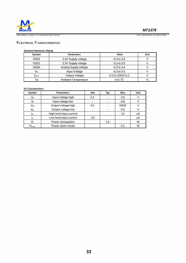
E LECTRICAL C HARACTERISTICS
Absolute Maximum Rating
Symbol Parameters Value Unit
VDD3 3.3V Supply voltage -0.3 to 3.6 V VDD2 2.5V Supply voltage -0.3 to 3.0 V VDDA Analog Supply voltage -0.3 to 3.6 V
VIN Input Voltage -0.3 to 5.5 V VOUT Output Voltage -0.3 to VDD3+0.3 V Ta Ambient Temperature 0 to 70 °C
DC Charateristics
Symbol Parameters Min Typ Max Unit
VIH Input voltage high 2.4 - 3.6 V VIL Input voltage low - - 0.8 V VOH Output voltage high 3.0 - VDD3 V VOL Output voltage low - - 0.5 V IIH High level input current 10 uA IIL Low level input current -10 uA PD Power dissapation 1.0 W
PDown Power down mode 0.1 W

This Data Sheet states AMD’s current technical specifications regarding the Product described herein. This DataSheet may be revised by subsequent versions or modifications due to changes in technical specifications.
Publication# 22358 Rev: B Amendment/+3Issue Date: November 10, 2000
16 Megabit (2 M x 8-Bit/1 M x 16-Bit) CMOS 3.0 Volt-only Boot Sector Flash Memory
DISTINCTIVE CHARACTERISTICS Single power supply operation
— Full voltage range: 2.7 to 3.6 volt read and write operations for battery-powered applications
— Regulated voltage range: 3.0 to 3.6 volt read and write operations and for compatibility with high performance 3.3 volt microprocessors
Manufactured on 0.23 µm process technology
— Fully compatible with 0.32 µm Am29LV160B device
High performance
— Access times as fast as 70 ns
Ultra low power consumption (typical values at 5 MHz)
— 200 nA Automatic Sleep mode current
— 200 nA standby mode current
— 9 mA read current
— 20 mA program/erase current
Flexible sector architecture
— One 16 Kbyte, two 8 Kbyte, one 32 Kbyte, and thirty-one 64 Kbyte sectors (byte mode)
— One 8 Kword, two 4 Kword, one 16 Kword, and thirty-one 32 Kword sectors (word mode)
— Supports full chip erase
— Sector Protection features:
A hardware method of locking a sector to prevent any program or erase operations within that sector
Sectors can be locked in-system or via programming equipment
Temporary Sector Unprotect feature allows code changes in previously locked sectors
Unlock Bypass Program Command
— Reduces overall programming time when issuing multiple program command sequences
Top or bottom boot block configurations available
Embedded Algorithms
— Embedded Erase algorithm automatically preprograms and erases the entire chip or any combination of designated sectors
— Embedded Program algorithm automatically writes and verifies data at specified addresses
Minimum 1,000,000 write cycle guarantee per sector
20-year data retention at 125°C
— Reliable operation for the life of the system
Package option
— 48-ball FBGA
— 48-pin TSOP
— 44-pin SO
CFI (Common Flash Interface) compliant
— Provides device-specific information to the system, allowing host software to easily reconfigure for different Flash devices
Compatibility with JEDEC standards
— Pinout and software compatible with single-power supply Flash
— Superior inadvertent write protection
Data# Polling and toggle bits
— Provides a software method of detecting program or erase operation completion
Ready/Busy# pin (RY/BY#)
— Provides a hardware method of detecting program or erase cycle completion (not available on 44-pin SO)
Erase Suspend/Erase Resume
— Suspends an erase operation to read data from, or program data to, a sector that is not being erased, then resumes the erase operation
Hardware reset pin (RESET#)
— Hardware method to reset the device to reading array data
Am29LV160D
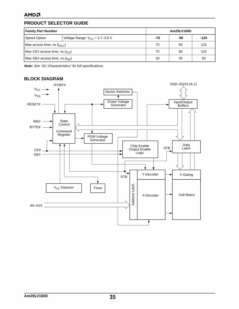
PRODUCT SELECTOR GUIDE
Note: See “AC Characteristics” for full specifications.
BLOCK DIAGRAM
Family Part Number Am29LV160D
Speed Option Voltage Range: VCC = 2.7–3.6 V -70 -90 -120
Max access time, ns (tACC) 70 90 120
Max CE# access time, ns (tCE) 70 90 120
Max OE# access time, ns (tOE) 30 35 50
Input/OutputBuffers
X-Decoder
Y-Decoder
Chip EnableOutput Enable
Logic
Erase VoltageGenerator
PGM VoltageGenerator
TimerVCC Detector
StateControl
CommandRegister
VCC
VSS
WE#
BYTE#
CE#OE#
STB
STB
DQ0–DQ15 (A-1)
Sector Switches
RY/BY#
RESET#
DataLatch
Y-Gating
Cell Matrix
Add
ress
Lat
ch
A0–A19

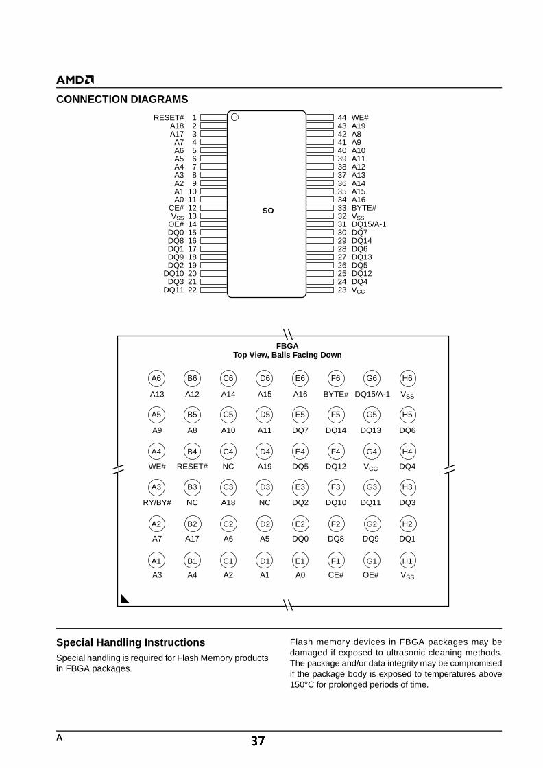
CONNECTION DIAGRAMS
A1
A15
A18
A14A13A12A11A10A9A8A19NCWE#RESET#NCNCRY/BY#
A17A7A6A5A4A3A2
1
16
2345678
1718192021222324
9101112131415
A16
DQ2
BYTE#VSS
DQ15/A-1DQ7
DQ14DQ6
DQ13
DQ9DQ1DQ8DQ0OE#VSSCE#
A0
DQ5DQ12
DQ4VCC
DQ11DQ3
DQ10
48
33
4746454443424140393837363534
25
32313029282726
A1
A15
A18
A14A13A12A11A10
A9A8
A19NC
WE#RESET#
NCNC
RY/BY#
A17A7A6A5A4A3A2
1
16
2345678
1718192021222324
9101112131415
A16
DQ2
BYTE#VSSDQ15/A-1DQ7DQ14DQ6DQ13
DQ9DQ1DQ8DQ0OE#VSSCE#A0
DQ5DQ12DQ4VCCDQ11DQ3DQ10
48
33
4746454443424140393837363534
25
32313029282726
Reverse TSOP
Standard TSOP
A
CONNECTION DIAGRAMS
Special Handling InstructionsSpecial handling is required for Flash Memory productsin FBGA packages.
Flash memory devices in FBGA packages may bedamaged if exposed to ultrasonic cleaning methods.The package and/or data integrity may be compromisedif the package body is exposed to temperatures above150°C for prolonged periods of time.
123456789
10111213141516171819202122
RESET#A18A17
A7A6A5A4A3A2A1A0
CE#VSS
OE#DQ0DQ8DQ1DQ9DQ2
DQ10DQ3
DQ11
44434241403938373635343332313029282726252423
WE#A19A8A9A10A11A12A13A14A15A16BYTE#VSSDQ15/A-1DQ7DQ14DQ6DQ13DQ5DQ12DQ4VCC
SO
A1 B1 C1 D1 E1 F1 G1 H1
A2 B2 C2 D2 E2 F2 G2 H2
A3 B3 C3 D3 E3 F3 G3 H3
A4 B4 C4 D4 E4 F4 G4 H4
A5 B5 C5 D5 E5 F5 G5 H5
A6 B6 C6 D6 E6 F6 G6 H6
DQ15/A-1 VSSBYTE#A16A15A14A12A13
DQ13 DQ6DQ14DQ7A11A10A8A9
VCC DQ4DQ12DQ5A19NCRESET#WE#
DQ11 DQ3DQ10DQ2NCA18NCRY/BY#
DQ9 DQ1DQ8DQ0A5A6A17A7
OE# VSSCE#A0A1A2A4A3
FBGATop View, Balls Facing Down
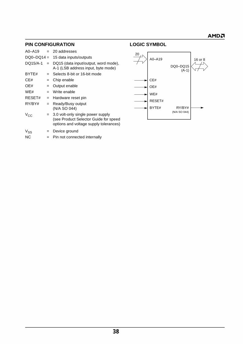
PIN CONFIGURATIONA0–A19 = 20 addresses
DQ0–DQ14 = 15 data inputs/outputs
DQ15/A-1 = DQ15 (data input/output, word mode), A-1 (LSB address input, byte mode)
BYTE# = Selects 8-bit or 16-bit mode
CE# = Chip enable
OE# = Output enable
WE# = Write enable
RESET# = Hardware reset pin
RY/BY# = Ready/Busy output (N/A SO 044)
VCC = 3.0 volt-only single power supply(see Product Selector Guide for speedoptions and voltage supply tolerances)
VSS = Device ground
NC = Pin not connected internally
LOGIC SYMBOL
20
16 or 8
DQ0–DQ15(A-1)
A0–A19
CE#
OE#
WE#
RESET#
BYTE# RY/BY#(N/A SO 044)
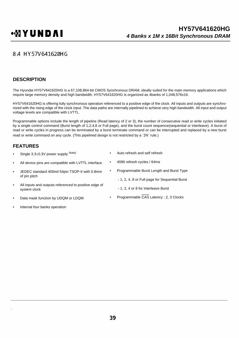
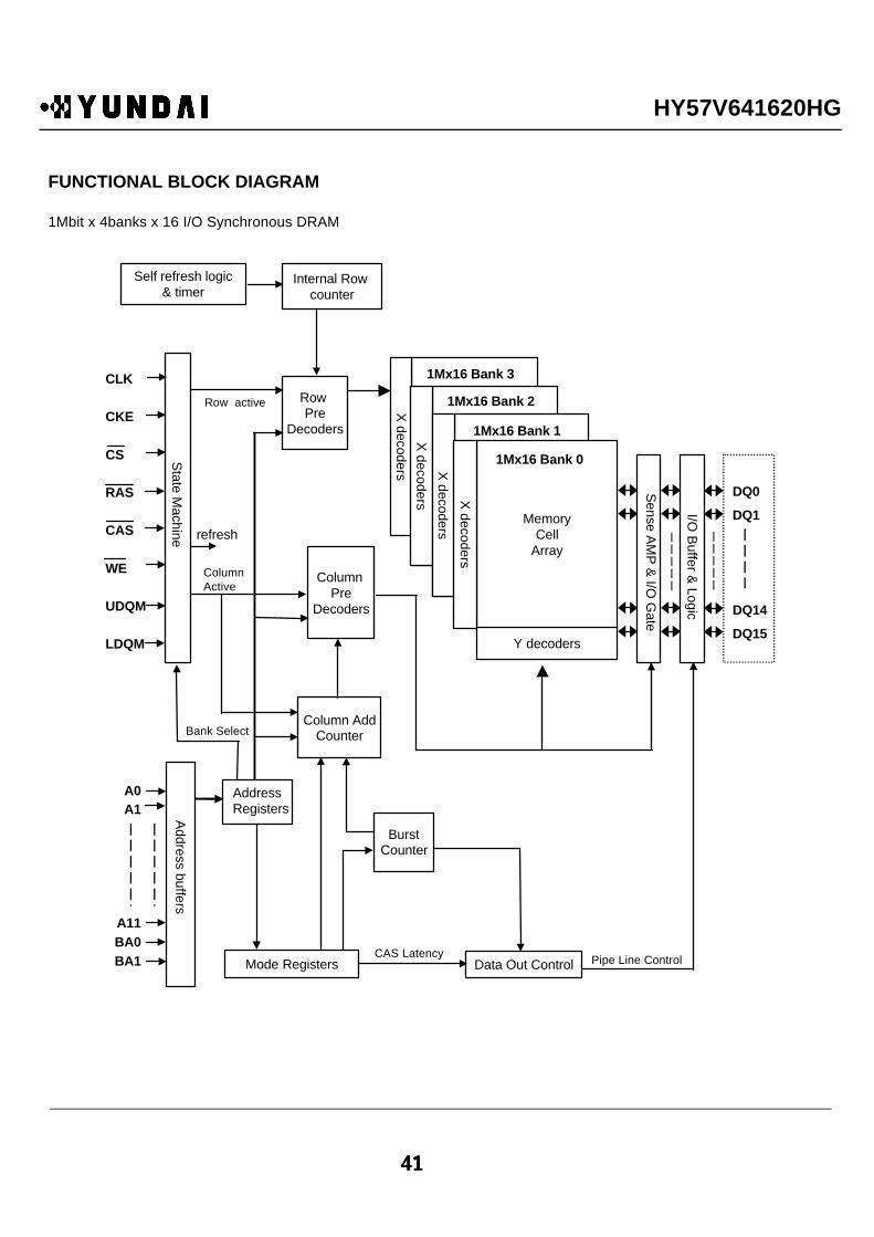
HY57V641620HG4 Banks x 1M x 16Bit Synchronous DRAM
.
DESCRIPTION
The Hyundai HY57V641620HG is a 67,108,864-bit CMOS Synchronous DRAM, ideally suited for the main memory applications whichrequire large memory density and high bandwidth. HY57V641620HG is organized as 4banks of 1,048,576x16.
HY57V641620HG is offering fully synchronous operation referenced to a positive edge of the clock. All inputs and outputs are synchro-nized with the rising edge of the clock input. The data paths are internally pipelined to achieve very high bandwidth. All input and outputvoltage levels are compatible with LVTTL.
Programmable options include the length of pipeline (Read latency of 2 or 3), the number of consecutive read or write cycles initiatedby a single control command (Burst length of 1,2,4,8 or Full page), and the burst count sequence(sequential or interleave). A burst ofread or write cycles in progress can be terminated by a burst terminate command or can be interrupted and replaced by a new burst
read or write command on any cycle. (This pipelined design is not restricted by a `2N` rule.)
FEATURES
• Single 3.3±0.3V power supply Note)
• All device pins are compatible with LVTTL interface
• JEDEC standard 400mil 54pin TSOP-II with 0.8mm of pin pitch
• All inputs and outputs referenced to positive edge of system clock
• Data mask function by UDQM or LDQM
• Internal four banks operation
• Auto refresh and self refresh
• 4096 refresh cycles / 64ms
• Programmable Burst Length and Burst Type
- 1, 2, 4, 8 or Full page for Sequential Burst
- 1, 2, 4 or 8 for Interleave Burst
• Programmable CAS Latency ; 2, 3 Clocks
HY57V641620HG
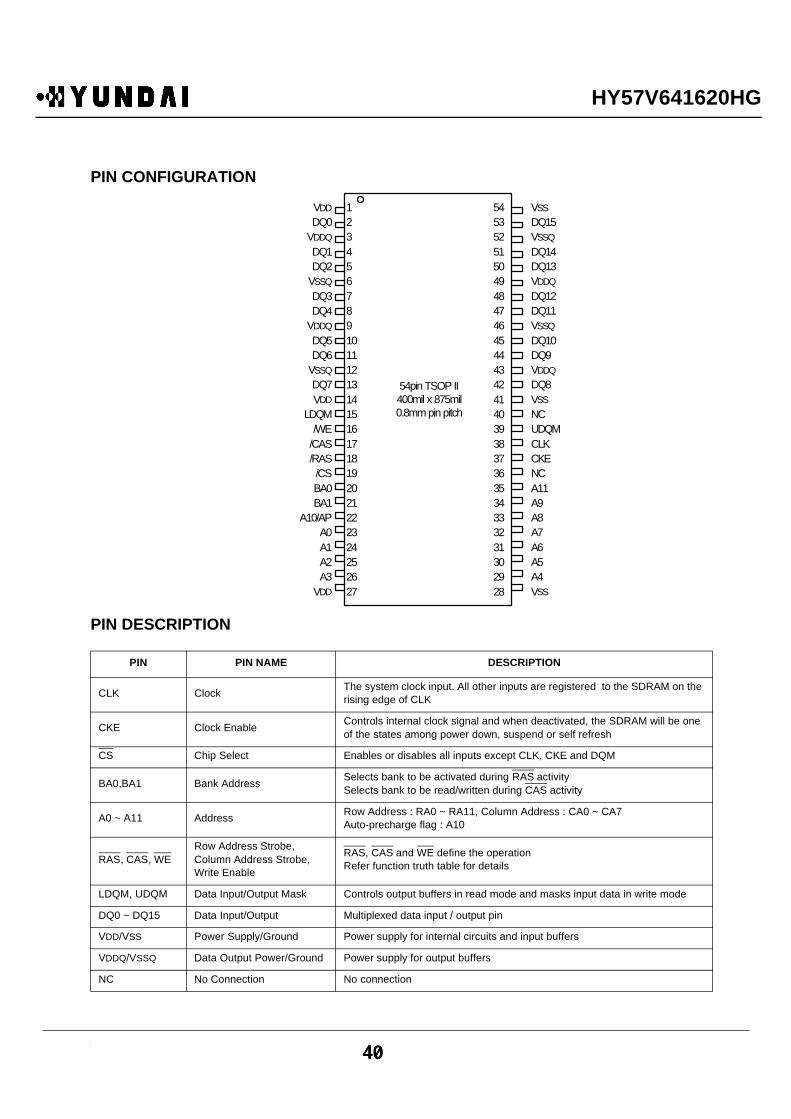
PIN CONFIGURATION
PIN DESCRIPTION
PIN PIN NAME DESCRIPTION
CLK ClockThe system clock input. All other inputs are registered to the SDRAM on the rising edge of CLK
CKE Clock EnableControls internal clock signal and when deactivated, the SDRAM will be one of the states among power down, suspend or self refresh
CS Chip Select Enables or disables all inputs except CLK, CKE and DQM
BA0,BA1 Bank Address
Selects bank to be activated during RAS activitySelects bank to be read/written during CAS activity
A0 ~ A11 AddressRow Address : RA0 ~ RA11, Column Address : CA0 ~ CA7Auto-precharge flag : A10
RAS, CAS, WERow Address Strobe, Column Address Strobe, Write Enable
RAS, CAS and WE define the operationRefer function truth table for details
LDQM, UDQM Data Input/Output Mask Controls output buffers in read mode and masks input data in write mode
DQ0 ~ DQ15 Data Input/Output Multiplexed data input / output pin
VDD/VSS Power Supply/Ground Power supply for internal circuits and input buffers
VDDQ/VSSQ Data Output Power/Ground Power supply for output buffers
NC No Connection No connection
VSS
DQ15VSSQ
DQ14DQ13VDDQ
DQ12DQ11VSSQ
DQ10DQ9VDDQ
DQ8VSS
NCUDQMCLKCKENCA11A9A8A7A6A5A4VSS
123456789101112131415161718192021222324252627
545352515049484746454443424140393837363534333231302928
VDD
DQ0VDDQ
DQ1DQ2
VSSQ
DQ3DQ4
VDDQ
DQ5DQ6
VSSQ
DQ7VDD
LDQM/WE
/CAS/RAS/CSBA0BA1
A10/APA0A1A2A3
VDD
54pin TSOP II400mil x 875mil0.8mm pin pitch
HY57V641620HG
FUNCTIONAL BLOCK DIAGRAM
1Mbit x 4banks x 16 I/O Synchronous DRAM
X decoders
State M
achine
A0A1
A11BA0BA1
Address buffers
AddressRegisters
Mode Registers
Row Pre
Decoders
Column Pre
Decoders
Column AddCounter
Row active
ColumnActive
BurstCounter
Data Out ControlCAS Latency
Internal Row counter
DQ0
DQ1
DQ14
DQ15
refresh
Self refresh logic& timer
Pipe Line Control
I/O B
uffer & Logic
Bank Select
Sense A
MP
& I/O
Gate
CLK
CKE
CS
RAS
CAS
WE
UDQM
LDQM
1Mx16 Bank 3
X decoders
X decoders
MemoryCell
Array
Y decoders
X decoders
1Mx16 Bank 0
1Mx16 Bank 1
1Mx16 Bank 2
12
3
12
34
56
A B C D E
A B C D E F
K40
4
K40
3
K40
1
K40
2
12
VD
401
1N41
48
P1/S
11
P2/S
22
P3/S
33
P4/S
44
S55
S66
S77
S88
S99
S10
10
S11
11
S12
12
S13
13
S14
14
S15
15
S16
16
S17 17
S18 18
S19 19
S20 20
S21 21
S22 22
S23 23
S24 24
S25 25
S26 26
S39
39
S38
38
S37
37
S36
36
S35
35
S34
34
S33
33
S32 32S31 31S30 30S29 29S28 28S27 27
KI352
KI251
KI150
KS649
KS5
48
KS4
47
KS3
46
KS2
45
KS1
44
CO
M4
43
CO
M3
42
CO
M2
41
CO
M1
40
KI453 KI554 TEST55 VDD56 VDD157
VSS59 OSD60 DO61 CE62 CL63 DI64
VDD258 U40
2
PT65
54LQ
KS5
KS4
KS3
KS2
KS1
CO
M4
CO
M3
CO
M2
CO
M1
CO
M1
CO
M2
CO
M3
CO
M4
S5 S6 S7 S8 S9 S10
S11
S12
S13
S14
S15
S16
C40
110
3
TC40
147
uF/1
6V
DO
CE
CL
DI
C40
510
1
C40
468
1
R40
34.
7K
R40
462
K
+5V
+5V
R40
575
R
+5V
+5V
GN
DC
EC
LD
ID
O
C40
3
103
C40
2
103
(DN
S)(D
NS)
B
C E
Q40
180
50D
R40
11K
R40
247
0R
+5V
S17
P1/S
1
S18
234 1567
XS4
01X
S07
IR
A K
LED
402
A K
LED
403
12
R40
60R
R40
8R
409
S19
R41
5
1K
TC40
247
uF/1
6V
Q40
280
50D
P2/S
2
P2/S
2
LED
#
CO
M4
19C
OM
318
CO
M2
17C
OM
116
S15
15S1
414
S13
13S1
212
S11
11
S11
S22
S33
S44
S55
S66
S77
S88
S99
S10
10
U40
1
LCD
Vcc
3
GN
D2
OU
T1
U40
3H
S003
8B3V
C40
810
3TC
403
47uF
/16V
R40
710
0R
+5V
IR
21X
S402
XS0
2LE
D#
GN
D
VD
D1
RSW
2
CS
3
LX4
GN
D5
VB
6V
A7
REL
8U
404
IMP8
03
C40
710
4/10
0V
C40
610
1
R41
12M
R41
033
0KR
412
2K
12
VD
402
1N41
48
L401
560u
H
+5V
P2/S
2
21X
S403
XS0
2
ELA
ELB
ELB
ELA
K40
5
K40
6
KS6
R41
3
R41
64.
7KR
417
4.7K
R41
84.
7K
13
2
LED
401
R-G
LED
B
C E
Q40
380
50D
R42
11K
R41
947
0R
+5V
R42
0
B
C E
Q40
480
50D
R42
31K
R42
247
0R
+5V
12
3
12
34
56
A B C D E
A B C D E F
R70
3
68R
VIN
1
VC
C2
GN
D3JK
705
OPT
ICA
L
VC
C
Pr
L710
FBSM
T
L709
FBSM
T
L708
FBSM
T
L707
FBSM
T
Y1
Pb
VG
ND
GR
EEN
BLU
E
RED
BG R
LFE
AG
ND
VG
ND
VG
ND
LFE
CC
SRSLRL
VIE
DO
PbY1
PrVC
CSP
DIF
VIE
DO
CC
SRSL RL
BLA
CK
L701
FB L702
FB L703
FB L704
FB L705
FB L706
FB
C70
110
2
C70
210
2
C70
310
2
C70
410
2
C70
510
2
C70
610
2
C71
110
4
Y-
Pb-
SPD
IF
R70
62.
2R
L712
FBSM
T
L711
FBSM
T
Pr-
12
3 4
JK70
3S-
VID
EO
R70
122
0RC
710
104
R70
2
100R
SPD
IF
Y C
Y C
LEF#
CC
# SR#
SL# R#L#
C71
220
pF
C71
320
pF
C70
920
pF
C71
420
pF
C71
510
4
VG
ND
TC70
710
00uF
/10V
AG
ND
123JK
701
POW
ER S
UPP
LY
C71
8
104
TC70
822
0uF/
16V
+10V
12
43
L713
IND
UC
TOR
2
2 3 41 5 6 8 9 107 11 12 14 15 1613 17 18 20 21 2219 23 24 25 26
XS7
01
XS2
6
L714
10uH
/2A
+10V
TC71
147
0UF/
16V
VD
701
1N58
19R
707
10K
C72
1
103
C72
210
4TC
710
470u
F/16
VD
GN
D
R70
810
K
R70
930
K
TC70
947
uF/2
5V
DG
ND
DG
ND
DG
ND
BS
1
Vin
2
Vsw
3
GN
D4
Sync
8
EN7
Com
p6
FB5
U70
1
ZA30
20
C72
322
3
C72
010
1
L716
10uH
/2A
L715
22uH
/2A
C71
910
4
DG
ND
AG
ND
VG
ND
12 11 101314
15
JK70
2V
-OU
T2
2 3 41X
S702
XS0
4
DG
ND
+10V +5
VV
CC
3.3L7
1710
uH
R70
40R
(DN
S)
C71
620
pFC
717
20pF
+5V
1 2
JK70
4
VO
UT5
3 4
JK70
4
VO
UT6
C72
610
4
TC71
4
100u
F/16
V
C72
910
4
R71
53.
9K
R71
4
3.9K
TC71
2
47uF
/25V
TC71
510
0uF/
16V
C72
810
4
R71
0
3.9K
R71
1
3.9K
TC71
3
47uF
/25V
L
VC
C
R71
84.
7R
R71
94.
7R
AG
ND
C72
710
4
OUT1 1IN1- 2IN1+ 3GND 4
VDD8 OUT27 IN2-6 IN2+5
U70
2TD
A13
08
R71
23.
3K
R71
33.
9K
AG
ND
VC
C
R71
710
K
R71
610
K
C72
410
4(D
NS)
C72
510
4(D
NS)
TC716100uF/16V(DNS)
AG
ND
R
C73
0
104
C73
1
104
2 3 1
JK71
0
PHO
NEJ
AC
K3A
2 3 1
JK70
9
PHO
NEJ
AC
K3A
2 3 1
JK70
8
PHO
NEJ
AC
K3A
231JK
707
PHO
NEJ
AC
K3A
R72
01K R
721
56K
R72
21K R
723
56K
TC71
710
00uF
/16V
1 2C73
2
104
DG
ND
R72
5
0R R72
6
0R
R72
7
0R R72
8
0R R72
9
0R R73
0
0R

12
3
12
34
56
A B C D E
A B C D E F
WO
BSO
1W
VD
D2
AG
ND
X3
AG
ND
X4
AV
DD
O5
RFO
P6
RFO
N7
AG
ND
O8
TM1
9TM
210
TM3
11A
GN
DT
12TM
413
AV
DD
T14
V2R
EFO
15V
REF
O16
V20
17FE
O18
LVL
19C
SO20
TEO
21V
DD
P22
DEF
ECT
23LR
FRP
24H
RFR
P25
CR
TP26
CR
TPLP
27TR
LPA
28TR
LP29
HTR
C30
GN
DP
31D
PFN
32D
PFO
33A
GN
DX
34A
GN
DX
35A
GN
DX
36V
DD
37V
FO13
38
GND39 UDGATE40 HDGATE41 IO042 IO143 IO244 IO345 IO446 IO547 IO648 IO749 IO850 IO951 IOA52 IOB53 VDDS54 XCK16M55 SCLK56 GNDS57 SDEN58 SDATA59 RST60 DPDMUTE61 AGNDP62 AGNDX63 AVDDP64
AG
ND
F65
VC
ON
66
AV
DD
F67
AG
ND
X68
AV
DD
M69
CO
SPH
I70
HA
LLC
OS
71
REF
CO
S72
IR 108AGND 107SB 106SA 105MD 104MC 103
MB
102
MA
101
DV
DA
100
DV
DB
99D
VD
C98
DV
DD
97D
VD
RFI
P96
DV
DR
FIN
95C
DA
94C
DB
93C
DC
92C
DD
91O
SN90
OSP
89R
FFG
C88
RFG
CU
87R
FGC
I86
CEO
P85
CEO
N84
AG
ND
X83
AG
ND
X82
MO
N81
MO
P80
SW1
79SW
278
SW0
77SI
NPH
I76
REF
SIN
75H
ALL
SIN
74A
GN
DM
73
AVDD 109
SC 110
SD 111
CDFOP 112
CDFON 113
SVDD 114
TPI 115
TNI 116
SGND 117
WGAND 118
AGC1 119
WAVDD 120
AGC2 121
AGC3 122
MD12 123
MD11 124
LDO1 125
LDO2 126
RFSUBO 127
WGND 128
U30
1
MT1
376E
_128
RFO
NR
FOP
C30
110
4C
302
104
C30
310
4TC
306
10uF
/16V
TC30
710
uF/1
6V
V2P
8V
1P4
V20
FEO
RFL
CSO
TEO
BD
O
C30
439
1C
305
82pF
C30
633
3C
307
471(
DN
S)
R30
110
0K(D
NS)
RFR
PC
RTP
C30
815
3C
309
10pF
(DN
S)
HTR
C
C31
027
pF(D
NS)
R30
227
K(D
NS)
TRIN
LIMIT
ENDMIOA
SCLK
SDENSDATAURST
PWMOUT2
OPO
OP-
OP+
C31
147
1
C31
210
4
C31
310
4
C31
510
5
C31
610
5
C31
710
5
C31
810
5
C31
410
5(D
NS)
RFO
D A B C C B
DD
1
BB
1A
A1
A D
C32
310
4
C31
915
3R
307
15K
MD11
LDO2LDO1
R30
510
KR
306
10K
END
MST
BY
C32
210
4C
320
104
C32
110
4TC
305
47uF
/16V
C32
410
4
C32
710
4
C32
510
4
C32
610
4
RV
CC
IN
RV
CC
IN
C33
810
4C
339
104
234 1568910 71112141516 131718202122 192324
XS3
0124
P0.5
mm
R32
020
KR
319
10K
R32
120
KC
331
151
C33
710
4
C33
510
4C
336
104
TC30
447
uF/1
6V
R31
81R
R31
71R
R31
620
K
C33
010
4
L318
FBSM
T
L316
FBSM
T
L312
FBSM
TL3
14FB
SMT
L311
FBSM
TL3
10FB
SMT
L308
FBSM
TL3
07FB
SMT
L306
10uH
L305
FBSM
TL3
04FB
SMT
L303
10uH
L319
FBSM
TL3
20FB
SMT
L321
FBSM
TL3
22FB
SMT
L323
FBSM
TL3
24FB
SMT
C32
810
4TC
301
220u
F/16
V
C32
910
4
AV
CC
E A
V30
12S
B11
32-S
V30
22S
B11
32-S
R31
415
R
R31
515
R
TC30
247
uF/1
6V
TC30
347
uF/1
6V
LDO
-AV
CC
LDO
-AV
CCLD
O2
LDO
1
R30
9
10K
R30
8
100K
R31
1
10K
R31
0
100K
R31
31R
R31
21R
C33
415
1
RFV
CC
FE
STBY
R33
70R
L301
FBSM
T
MD
11
V30
32S
K30
18-S
V30
42S
K30
18-S
V30
539
04-S
IOA
AV
CC
F
L317
FBSM
T
B RFO
IOA
D C
VIN
FC1
CF1
2C
F23
VIN
SL+
4V
INSL
-5
VO
SL6
VIN
FFC
7
GND30
VC
C8
PVC
C1
9PG
ND
10V
OSL
-11
VO
2+12
VO
FC-
13V
OFC
+14
VO
TK+
15
VO
TK-
16
VO
LD+
17
VO
LD-
18
PGN
D19
VN
FTK
20
PVC
C2
21
GND29
PRE
GN
D22
VIN
LD23
CTK
224
CTK
125
VIN
TK26
BIA
S27
STB
Y28
U30
2B
A59
54
TR
SOV
1P4
STB
Y
SL+
SL-
FMSO
VC
C
GN
D
VC
C
SP-
SP+
V1P
4
FOSO
DM
SO
V20
C34
210
1
R32
40R
(DN
S)R
325
0R(D
NS)
GN
D
R33
61R
R33
333
0KR
334
330K
R33
575
0K
R33
1
750K
R33
20R
C33
327
pF
AD
INO
P-O
P+
V1P
4
SP+
SP-
SL+
SL-
LIM
IT
OPO
C34
110
4
2 3 41 5 6
XS3
03X
S06
TC30
810
uF/1
6V
RV
CC
IN
R32
7D
NS
R32
6D
NS
HSY
NC
#SW
1
SW1
DV
33L3
25FB
SMT
L326
FBSM
T
R32
80R
(DN
S)
R32
9D
R(D
NS)
RV
CC
IN
RFV
CC
VC
C
RV
CC
L327
FBSM
T
R33
0D
R(D
NS)
LDO
-AV
CC
AV
CC
R30
410
KR
303
10K
TRC
LOSE
TRO
PEN
TROUT
TRCLOSE
2 31
XS3
02X
S03
TRO
UT
TRIN
CC
1
R32
247
0RR
323
470R
V30
880
50
V30
780
50
V30
685
50V
309
8550
R34
31.
5KR
342
1.5K
R34
5
10K
R34
44.
7R\1
/4W
TC31
047
uFTC
309
47uF
LOA
D+
LOA
D-
LOA
D-V
CC
TRO
PEN
TRC
LOSE
V31
090
14
TRO
PEN
(TR
CLO
SE1)
(TR
OPE
N1)
(TR
CLO
SE1)
21X
S305
XS0
2
LOA
D-
LOA
D+
C34
410
4
C34
3
104
ADJ 1
OU
T2
IN3
U30
4LM
1117
MP-
2.5
R34
6
150R
R34
747
0R
TC31
210
uF/1
6VC
345
104
+10V
LOA
D-V
CC
C34
610
4
C34
810
4
R34
84.
7R\1
/4W
C35
010
4C
349
104
TC31
347
uF/1
6V
+10V
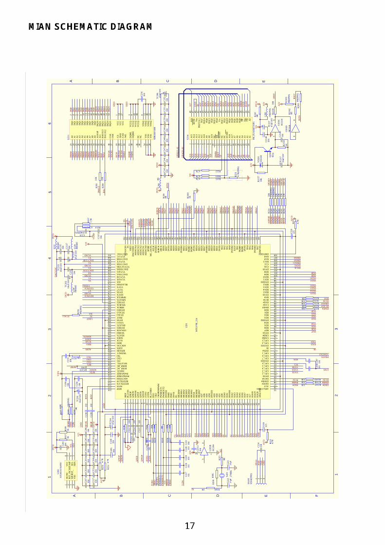
12
3
12
34
56
A B C D E
A B C D E F
C21
210
3C
213
103
C21
410
3
C21
510
3
C21
610
1R
202
750K
R20
320
KR
204
18K
R20
50R
R20
610
KR
207
15K
R20
18.
2K
C22
110
4C
220
153
C21
910
3C
218
331
C21
733
1
V1P
4
FMSO
DM
SO
PWM
OU
T2
TR
SOFO
SO
JITF
O
LPFO
P
LPFI
P
C22
622
5
R21
24.
7R
C22
822
5R
213
4.7RA
V33
R2144.7R(DNS)
C229104(DNS)
Y2
DACV33AY4
Y5
VSYNC#
HSYNC#
Y7
Y6
SDATASDEN
R216 18K
C23
110
4
C23
010
4
C233102
C23
410
4
C23
810
2
C23
910
2R
FOP
RFO
NR
FIN
RFI
P
FEORFL
R21
9 0R
RFRPC
R21
80R
(DN
S)
RFZC
HTR
CC
232
104
AV
33
DV
33
C20
210
4C
203
104
C20
410
4C
205
104
C20
610
4C
207
104
C20
810
4C
209
104
C21
010
4C
211
104
V25
2 3 41
XS2
03X
S04(
DN
S)
DV
33R
XD
TXD
GN
D
C22
410
4
X20
1
27M
Hz
34
714
U20
5BH
CU
04R
208
100K
C22
227
pFC
223
27pF
A5V
TC20
647
uF/1
6V
C24
510
4C
246
104
C24
710
4C
248
104
C24
910
4C
250
104
C25
110
4C
252
104
SD33
L204
FBD
V33
GN
D
LPIO
NLP
IOP
RFR
PC
C21
1310
4
TC21
547
uF/1
6V
C21
3710
4
Q20
490
14
C21
4810
2TC
217
10uF
/16V
VD
201
1N41
48R
2157
10K
R21
581K
R21
5933
R5
6
U20
5CH
CU
04
UR
ST
A5V
R21
601K
C25
310
4
89
U20
5DH
CU
04
RSE
T
C24
010
4
GN
D
R21
620R
R21
630R
(DN
S)
A5V
ASD
ATA
315
7A
SDA
TA4
158
DA
CV
DD
C15
9V
REF
160
FS16
1Y
UV
0/C
IN16
2
DACVSSC163 YUV1/C164 DACVSSB165 YUV2/Y166 DACVSSB167 YUV3/CVBS168 DACVDDA169 YUV4/G170 DACVSSA171 YUV5/B172 YUV6/R173 ICE174 BLAANK#175 VSYN176 YUV7177 DVSS178 HSYN179 SPMCLK180 SPDATA181 DVDD2182 SPLRCK183 SPBCK184 DVDD3185 XTALO186 XTALI187 PRST188 DVSS189 VFO13190 IDGATE191 DVDD3192 UDGATE193 WOBSI194 SDATA195 SDEN196 SLCK197 BDO198 ADCVSS199 ADIN200 RFSUBI201 TEZISLV202 TEI203 CSO204 FEI205 RFLEVEL206 RFRP_DC207 RFRP_AC208
APLLVDD3 55
ALE 56
IOOE# 57
IOWR# 58
IOCS# 59
DVSS 60
UP1_2 61
UP1_3 62
UP1_4 63
UP1_5 64
UP1_6 65
DVDD3 66
UP1_7 67
UP3_0 68
UP3_1 69
INT0# 70
IR 71
DVDD2 72
UP3_4 73
UP3_5 74
UWR# 75
URD# 76
DVSS 77
RD7 78
RD6 79
RD5 80
RD4 81
DVDD2 82
RD3 83
RD2 84
RD1 85
RD0 86
RWE# 87
CAS# 88
RAS# 89
RCS# 90
BA0 91
DVSS 92
RD15 93
RD14 94
RD13 95
RD12 96
DVDD3 97
RD11 98
RD10 99
RD9 100
RD8 101
DVSS 102
CLK 103
CLE 104
DM
VSS
109
RA
711
0D
VD
D3
111
RA
611
2R
A5
113
RA
411
4D
VSS
115
DQ
M1
116
DQ
M0
117
BA
111
8R
A10
119
DV
DD
212
0R
A0
121
RA
112
2R
A2
123
RA
312
4D
VSS
125
RD
3112
6R
D30
127
RD
2912
8R
D28
129
DV
DD
313
0R
D27
131
RD
2613
2R
D25
133
RD
2413
4D
VSS
135
DQ
M3
136
DQ
M2
137
RD
2313
8R
D22
139
DV
DD
214
0R
D21
141
RD
2014
2R
D19
143
RD
1814
4D
VSS
145
RD
1714
6R
D16
147
AB
CK
148
ALR
CK
149
DV
DD
315
0A
CLK
151
MC
_DA
TA15
2SP
DIF
153
ASD
ATA
015
4A
SDA
TA1
155
ASD
ATA
215
6
APL
LVSS
54IO
A20
53
IREF
1
PLLV
SS2
LPIO
N4
LPIO
P3
LPFO
N5
LPFI
P6
LPFI
N7
LPFO
P8
JITF
O9
JITF
N10
PLLV
DD
311
FOO
12
TRO
13
TR
OPE
NPW
M14
PWM
OU
T115
PWM
OU
T216
DV
DD
217
DM
O18
FMO
19
DV
SS20
FG21
HIG
HA
022
HIG
HA
123
HIG
HA
224
HIG
HA
325
HIG
HA
527
HIG
HA
426
DV
SS28
HIG
HA
629
HIG
HA
730
AD
731
AD
632
AD
533
DV
DD
335
AD
336
AD
434
AD
237
AD
138
AD
039
IOA
040
IOA
141
DV
DD
242
IOA
243
IOA
344
IOA
445
IOA
546
IOA
647
IOA
748
A16
49
A17
50
IOA
1851
IOA
1952
RA11 105
RA9 106
RA8 107
DMVDD3 108
HRFZC209 PWMVREF210 PWM2VREF211 ADCVDD3212 RFDTSLVP213 RFDTSLVN214 RFIN215 RFIP216
U20
1
MT1
379E
_216
JITF
N
V25
FG A8
A9
A10
A11
A12
A13
A14
A15
AD
7A
D6
AD
5A
D4
AD
3A
D2
AD
1A
D0
A0
A1
A2
A3
A4
A5
A6
A7
A16
A17
A18
A19
A20
DRD#DWR#DCE#
VSCKVSDAVSTBSCL
SDA
IR
RXDTXD
DQ7DQ6DQ5DQ4
DQ3DQ2DQ1DQ0
DCAS#DRAS#DCS#BA0
DQ15DQ14DQ13DQ12
DWE#
DQ11DQ10DQ9DQ8
DCLKDCKEDMA11DMA9DMA8
DM
A7
DM
A6
DM
A5
DM
A4
RD
QM
1R
DQ
M0
BA
1D
MA
10
DM
A0
DM
A1
DM
A2
DM
A3
DQ
31D
Q30
DQ
29D
Q28
DQ
27D
Q26
DQ
25D
Q24
RD
QM
3R
DQ
M2
DQ
23D
Q22
DQ
21D
Q20
DQ
19D
Q18
DQ
17D
Q16
AB
CK
ALR
CK
AC
LKA
MD
AT
ASP
DIF
ASD
AT0
ASD
AT1
ASD
AT2Y0
FSV
REF
VG
ND
R23
71.
5K
Y1DACV33B
Y3
R23
60R
(DN
S)
L329
FBSM
T
DV
33
URSTXIXO
XTALI
SCLKBDO
V2P
8
R21
710
0K
RFRP
CSOTEO
V1P
4
TC20
210
uF/1
6V
VGND
L330
FBSM
T
DV
33
DA
CV
33C
L331
FBSM
TTC
219
10uF
/16V
C23
510
4
DA
CV
33C
C23
710
4
XI R2400R
XO
V25
GN
D
AV
33DC
/NC
1
RST
_/N
C2
WP/
RST
_3
VSS
4
VC
C8
RST
/WP
7
SCL
6
SDA
5
U20
2A
T24C
02/X
4050
SDA
SCL
C20
110
4
DV
33
R22
71K
R22
81K
VGND
VGND
VGND
ADIN
C29
510
4
R25
24.
7R
R25
14.
7R
R210733RR210833RR210933R
R22933RR23033RR23133RR23233RR23333R
PRD#PWR#PCE#
R23
433
RD
CLK
SDC
LKR
235
33R
SDC
KE
DC
KE
R24
633
RR
247
33R
R24
833
R(D
NS)
R24
933
R(D
NS)
RD
QM
0R
DQ
M1
RD
QM
2R
DQ
M3
DQ
M3
DQ
M2
DQ
M1
DQ
M0
R25
433
RA
SPD
IFSP
DIF
#
VDATA3
TC20
110
uF/1
6V
C22
710
4
PWM
OU
T1
PDAT0
TC20
447
uF/1
6V
R25
5
0R
C29
610
1C
297
101
GND
A6
19
A17
17
RY
/BY
15
A18
16
NC
14
A12
4
NC
10
NC
13
A9
7
A15
1
A14
2
A13
3
A11
5
A10
6
A8
8
A19
9
WE
11
RES
ET12
A5
20
A4
21
A3
22
A7
18
DQ
830
DQ
932
DQ
1034
DQ
233
DQ
335
DQ
15/A
-145
DQ
1239
DQ
1136
DQ
642
A16
48
BY
TE47
Vss
46
DQ
744
DQ
1443
DQ
1341
DQ
540
DQ
438
Vcc
37
DQ
029
OE
28
Vss
27
DQ
131
A2
23
A1
24C
E26
A0
25
U21
4
8M_F
LASH
(TSO
P)
A15
A14
A13
A12
A11
A10
A9
DW
R#
RSE
T
A18
A7
A6
A5
A4
A3
A2
A16
GN
DA
0A
D7
AD
14A
D6
AD
13A
D5
AD
12A
D4
VD
AD
11A
D3
AD
10A
D2
AD
9A
D1
AD
8A
D0
DR
D#
GN
DD
CE#
A1
A8
UPA
[20.
.0]
UPD
[15.
.0]
R22
14.
7K(D
NS)
VP
R2224.7K
R2234.7KR2154.7K
VD
C21
4610
4
A17
A19
TC23
747
uF/1
6V
R22
00R
VD
DV
33
A20
L206
FB(D
NS)
A5V
R25
90R
RST
#
R26
00R
(DN
S)R
ST#
TRO
PEN
VSDA1
A0
23
A1
24
A2
25
A3
26
A4
29
A5
30
A6
31
A7
32
A8
33
A9
34
A10
/AP
22
A11
35
BA
0/A
1320
BA
1/A
1221
CLK
38
CK
E37
/CS
19
/RA
S18
/CA
S17
/WE
16
DQ
ML
15
DQ
MH
39
NC
36
NC
40
VSS
54
VSS
41
VSS
28
DQ
02
DQ
14
DQ
25
DQ
37
DQ
48
DQ
510
DQ
611
DQ
713
DQ
842
DQ
944
DQ
1045
DQ
1147
DQ
1248
DQ
1350
DQ
1451
DQ
1553
VC
C1
VC
C14
VC
C27
VC
CQ
3
VC
CQ
9
VC
CQ
43
VC
CQ
49
VSS
Q6
VSS
Q12
VSS
Q46
VSS
Q52
U21
1
SDR
AM
64M
DM
A0
DM
A1
DM
A2
DM
A3
DM
A4
DM
A5
DM
A6
DM
A7
DM
A8
DM
A9
DM
A10
MA
11B
A0
#BA
1
SDC
LKSD
CK
E
DC
S#D
RA
S#D
CA
S#D
WE#
DQ
M0
DQ
M1
DQ
0D
Q1
DQ
2
DQ
4D
Q5
DQ
6D
Q7
DQ
8D
Q9
DQ
10D
Q11
DQ
12D
Q13
DQ
14D
Q15
DQ
3
SD33
SD33
R28
433
R
R28
333
RD
MA
11
BA
1
C23
610
4

12
3
12
34
56
A C D E
A B C D E F
R28
115
0R
A5V
R28
015
0RC
269
47pF
C27
020
pF(D
NS)
C27
147
pF
L215
1.8u
H
VG
ND
VG
ND
R27
715
0R
A5V
VID
EO_U
R27
6
150R
C26
647
pF
C26
720
pF(D
NS)
C26
847
pF
L214
1.8u
H
VG
ND
VG
ND
VID
EO_V
R26
3
150R
A5V
R26
215
0RC
254
47pF
C25
520
pF(D
NS)
C25
647
pF
L210
1.8u
H
VG
ND
VG
ND
R27
515
0R
A5V
R27
415
0RC
257
47pF
C25
820
pF(D
NS)
C25
947
pF
L211
1.8u
H
VG
ND
VG
ND
R27
115
0R
A5V
R27
015
0RC
260
47pF
C26
120
pF(D
NS)
C26
247
pFL2
121.
8uH
VG
ND
VG
ND
R27
215
0R
A5V
VID
EO_Y
1
R27
315
0RC
263
47pF
C26
420
pF(D
NS)
C26
547
pF
L213
1.8u
H
VG
ND
VG
ND
1213
U20
5F
HC
U04
1011
U20
5E
HC
U04
L243
0R L244
0R L245
0R L246
0R L247
0R L248
0R
Q21
539
06-S
Q21
739
06-S
Q21
639
06-S
Q21
339
06-S
Q22
039
06-S
Q21
439
06-S
SPD
IF#
Y3
Y2
Y1
Y4
Y5
Y6
R25
7
0R
VID
EO_Y
VID
EO_C
Text
R22
4
0R(D
NS)
C21
4110
4C
2142
104
C21
4310
4TC
213
47uF
/16V
A5V
VG
ND
L224
FBL2
25FB
C28
210
4
C28
310
4
C28
410
4
TC20
310
0uF/
16V
TC20
722
0uF/
16V
+10V
DV
33
GN
D
L226
FBV
CC
VC
C3.
3
VC
C
A5V
C28
510
4TC
211
220u
F/16
V
C28
610
4TC
208
220u
F/16
V
L205
FB
AV
33 V25
Q20
180
50(D
NS)
RV
CC
L203
FBSM
T
L201
FBSM
TL2
02FB
SMT
R21
110
R
C22
5
47pF
GN
DV
STB
VSD
A
C24
447
pFC
242
47pF
C24
347
pF
R24
54.
7KA
5VL2
18FB
SMT
IR
L227
FB
AV
CC
ADJ 1
OU
T2
IN3
U20
9
LM11
17M
P-2.
5
R29
7
150R
R29
847
0RTC
255
10uF
/16V
C21
4410
4
A5V
V25
TC25
647
uFC
2140
104
DV
33
IN 1
GND 2
OUT 3
U20
8B
A03
3
C21
3210
4
VC
CL2
29
FB
A5V
TC23
910
0uF/
50V
R24
20R
(DN
S)
R24
10R
VC
CV
CC
3.3
234 1567X
S201
XS0
7
L217
FBSM
TV
SDA
1
VSC
K
C24
147
pF 234 1
XS2
02X
S04
IEC
958
VID
EO_C
OM
P
AG
ND
VG
ND
LFE
Cc#
SRSLRt
Lt
VID
EO_C
OM
P
VID
EO_U
VID
EO_V
VID
EO_C
VID
EO_Y
AA
5VIE
C95
8
VID
EO_Y
1
R25
615
0R
2 3 41 5 6 8 9 107 11 12 14 15 1613 17 18 20 21 2219 23 24 25 26
XS2
04
XS2
6
R25
00R
(DN
S)
+10V
IN 1
GND 2
OUT 3
U21
6W
S780
5(D
NS)
C21
4510
4
AA
5V
R28
5FB
SMT
R28
7FB
SMT
R28
6FB
SMT
R28
8FB
SMT
R28
9FB
SMT
R29
0FB
SMT
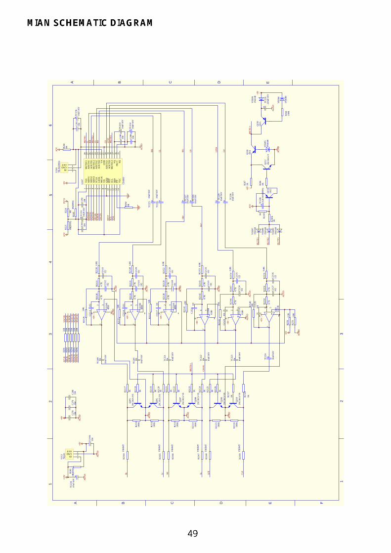
12
3
12
34
56
A B C D E
A B C D E F
+8V
R26
415
0R
R26
61K
VD
205
1N41
48
+8V
R26
71K
AG
ND
VD
206
1N41
48
MU
TE-1
TC23
522
0uF/
16V
AG
ND
Q21
22S
C18
15-Y
Q21
810
15
Q21
910
15
SR#
SL#
TC22
510
uF/1
6V
TC22
610
uF/1
6V
TC22
710
uF/1
6V
TC22
810
uF/1
6V
TC22
910
uF/1
6V
TC23
010
uF/1
6V
R21
50
4.7K
R21
51
4.7K
C21
2710
2
C21
2610
1R21
4924
K
R21
4124
K
C21
2010
1
C21
2110
2
R21
43
4.7K
R21
42
4.7K
R21
38
4.7K
R21
39
4.7K
C21
1810
2
C21
1710
1
R21
3724
K
R21
46
4.7K
R21
47
4.7K
C21
2410
2
C21
2310
1
R21
4524
K
R21
34
4.7K
R21
35
4.7K
C21
1510
2
C21
1410
1
R21
3324
K
R21
2924
K
C21
1110
1
C21
1210
2
R21
31
4.7K
R21
30
4.7K
+8V
+8V
+8V
+8V
+8V +8
V
321
48
U21
9A45
80
567
48
U21
9B45
80
321
48
U22
1A45
80
567
48
U22
0B45
80
321
48
U22
0A45
80 567
48
U22
1B45
80
AG
NDA
GN
D
AG
ND
AG
ND
AG
ND
AG
ND
AG
ND
TC22
4
10uF
/16V
TC22
3
10uF
/16V
TC22
2
10uF
/16V
TC22
1
10uF
/16V
TC24
0
10uF
/16V
TC24
1
10uF
/16V
CH
-SL
AG
ND
R21
23
1KR21
21
1KR21
201KR
2117
1K R21
24
1KR21
22
1KR21
19
1KR21
18
1K
R21
1110
0K
R21
1210
0K
R21
1310
0K
R21
1410
0K
MU
TE-1
Q20
82S
C18
15-Y
S
Q20
72S
C18
15-Y
S
Q20
52S
C18
15-Y
S
Q20
62S
C18
15-Y
S
R21
271K
R21
25
1K
R21
281K
R21
26
1K
R21
1510
0K
R21
1610
0KQ
210
2SC
1815
-YS
Q20
92S
C18
15-Y
S
SDA
TA2
SDA
TA1
SDA
TA0
SLR
CK
SAC
LK
SBC
LK
SCL
SDA
RST
#
LL RS
RR
LS LFE#
C#
R21
366.
8K
R21
486.
8K
R21
526.
8K
R21
536.
8K
R21
546.
8K
R21
556.
8K
C21
2212
2
C21
2912
2
C21
3012
2
C21
3312
2
C21
3512
2
C21
3612
2
VLS
1
SDIN
12
SDIN
23
SDIN
34
SCLK
5
LRC
K6
MC
LK7
VD
8
GN
D9
RST
10
SCL
11
SDA
12
CS
13
VLC
14
MU
TEC
128
AO
UTA
127
AO
UTB
126
MU
TEC
225
AO
UTA
224
AO
UTB
223
VA
22
GN
D21
AO
UTA
320
AO
UTB
319
MU
TEC
318
VQ
17
FILT
+16
M2
15
U20
7
CS4
360
C29
210
4C
293
104
DV
33
MU
TE1
C29
110
4TC
236
10uF
/16V
A5V
C28
910
4TC
232
10uF
/16V
C29
010
4TC
233
10uF
/16V
AG
ND
R28
20R
TC23
110
uF/1
6V
MU
TE2
MU
TE3
RS
LS LFE#
C#
MU
TE1
Q21
110
15R
2106
1K
R21
051K
VD
207
1N41
48
VD
208
1N41
48
VD
209
1N41
48
MU
TE2
MU
TE3
TC23
82.
2uF/
16V
(DN
S)
A5V
R22
5
0R(D
NS)
R22
6
0R
A5V
R29
133
RA
CLK
SAC
LKR
292
33R
R29
333
RR
294
33R
R29
533
RR
296
33R
AB
CK
SBC
LKA
LRC
KSL
RC
KA
SDA
T0SD
ATA
0SD
ATA
1SD
ATA
2A
SDA
T1A
SDA
T2
AG
ND
AG
ND
VD
204
1N41
48R
278
3.3K
R27
93.
9K
AG
ND
+8V
AG
ND
C27
810
4C
279
104
C28
010
4
+8V
AG
ND
IN 1
GND 2
OUT 3
U21
278
L08
+8V
AG
ND
C21
0410
4
R26
50R
(DN
S)TC
234
47uF
/16V A
GN
D
+10V
IN 1
GND 2
OUT 3
U21
078
L05(
DN
S)
+8V
R24
30R
(DN
S)
R24
40R
RR
LL
Rt
Lt SR SL LFE
Cc#
R21
64FB
SMT
R21
65FB
SMT
R21
66FB
SMT
R21
67FB
SMT
R21
68FB
SMT
R21
69FB
SMT
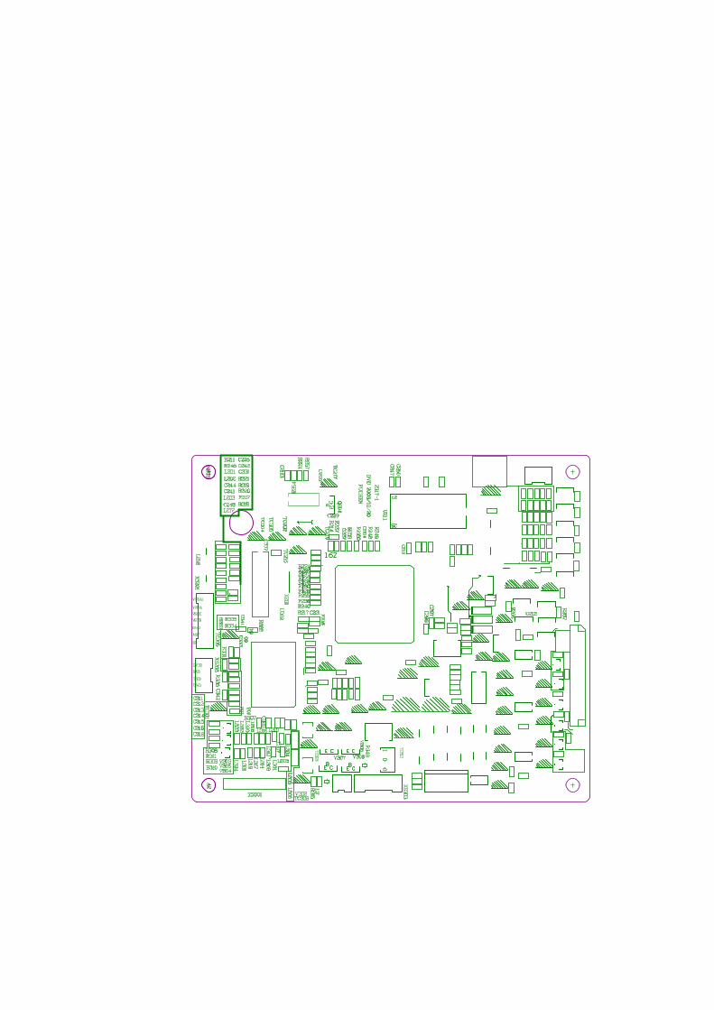
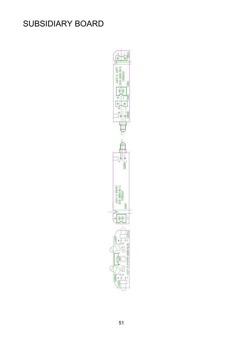
51
SUBSIDIARY BOARD
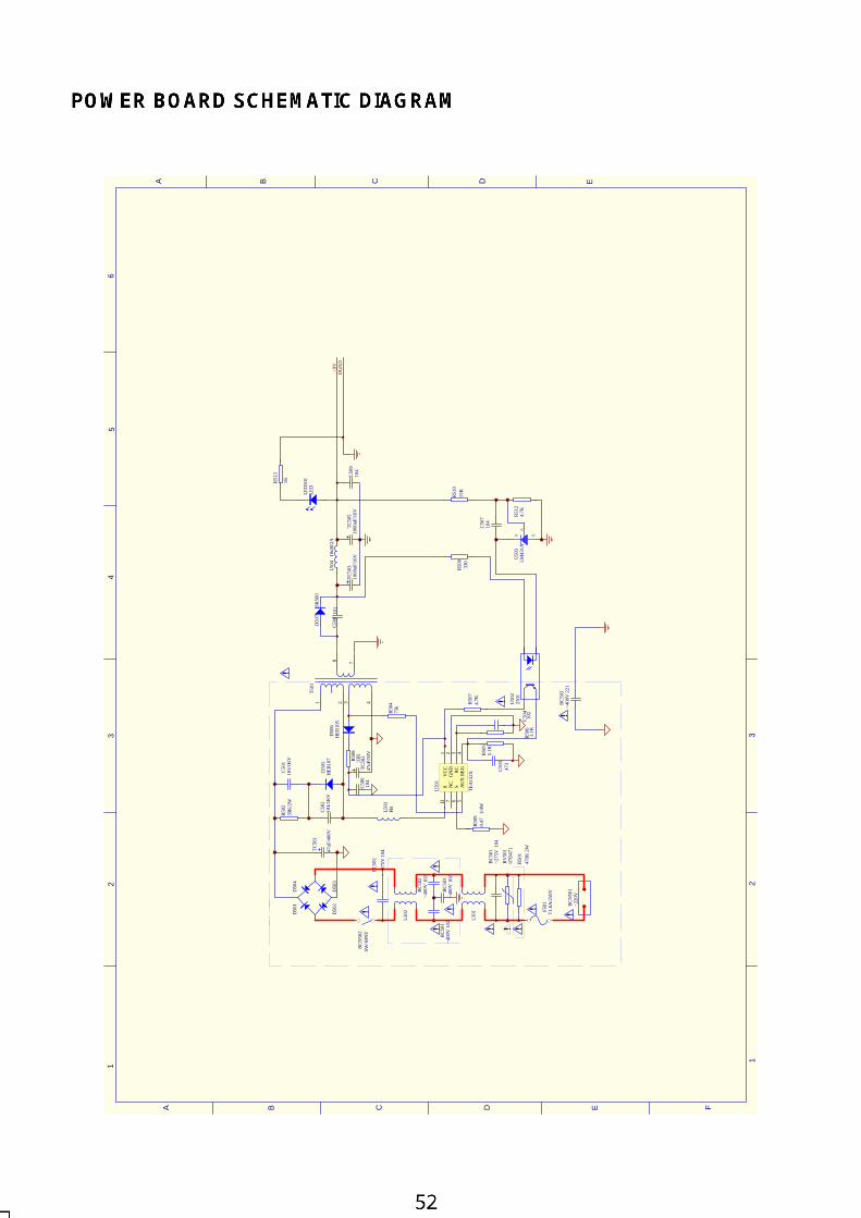
12
3
12
34
56
A B C D E
A B C D E F
U50
3LM
431A
C50
710
4
L504
10uH
/2A
BC
502
~275
V 1
04
BC
501
~275
V 1
04
BC
502
~400
V 1
02
BC
501
~400
V 1
02
L502
L501
RV
501
07D
471
F501
T1.6
A/2
50V
RK A
!
!
!
R51
24.
7K
R51
015
KR
509
330
R50
833
R
R50
239
K/2
W
!
BC
N50
2SW
-SPS
T
!!
U50
225
01
TC50
247
uF/5
0V
TC50
1
47uF
/400
VD
505
HER
107
C50
110
3/1K
V
C50
210
1/1K
V
L503
FB
DG
ND
+9V
BC
503
~400
V 2
21
BC
503
~400
V 1
02
C50
810
1
C50
610
4
TC50
310
00uF
/16V
TC50
510
00uF
/16V
R50
147
0K 2
W
!
!!
!
! ! !
~220
VB
CN
501
D50
1D
504
D50
2D
503
D50
6H
ER10
5
D50
7SR
560
C50
347
3
R50
475
k
R50
90.
47
1/4W
C50
410
2
VC
C1
GN
D2
RC
3
REG
4A
UX
5S
6N
C7
8D
U50
1
TEA
152X
R50
7 4
.7K
R50
55.
1K
R50
6 3.
1K
LED
501
LED
R51
3
1K
C50
910
4
1 2 3 4
8 7
T501
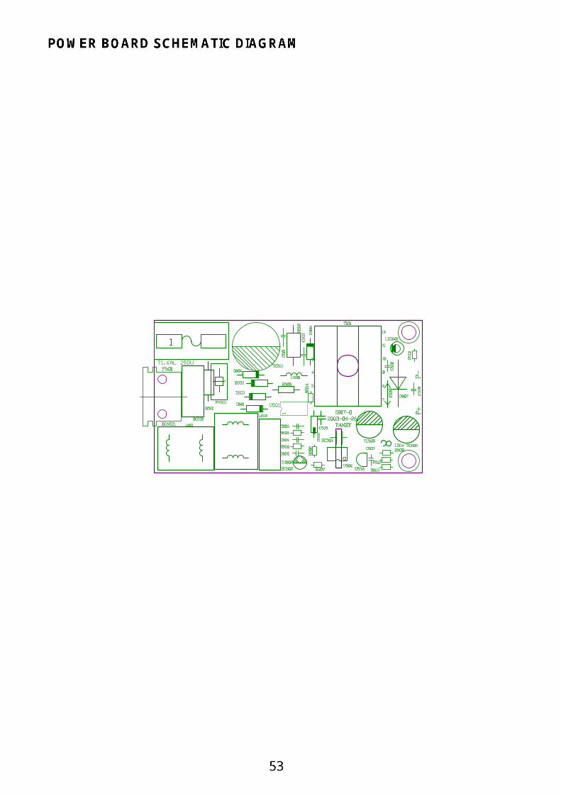
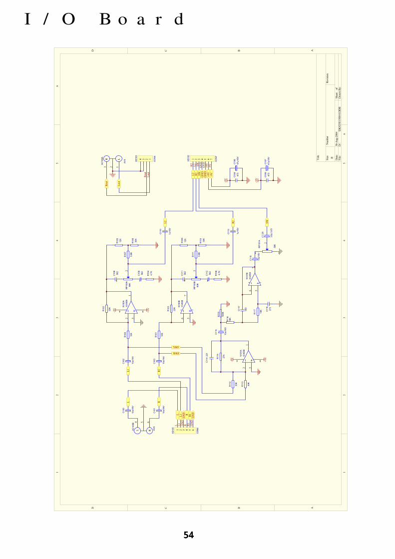
12
34
56
ABCD
65
43
21
D C B A
Titl
e
Num
ber
Rev
isio
nSi
ze B Dat
e:30
-Aug
-200
4Sh
eet
of
File
:D
:\\D
K92
5S\1
500-
0.D
DB
维修手册
Dra
wn
By:
L4 5
R6
XC
100B
AV
4
R10
0
10K
R10
1
10K
C10
2
10u/
16V
C10
3
10u/
16V
C10
0
10u/
16V
C10
1
10u/
16V
L R
567
N10
0BIC
4558
R10
3
22K
L1
R1
321
84
N10
0AIC
4558
R10
2
22K
C10
647
u/16
VC
104
473
C10
747
u/16
VC
105
473
+9V
-9V
567
N10
1BIC
4558
C11
827
3
R11
7
10KC
117
563
R11
618
K
321
84
N10
1AIC
4558
R11
2
30K
R11
3
30K
R11
4
27K
C11
5
10u/
16V
C11
422
1
C11
6
10u/
16V
SWL
SWR
SW
C10
856
2
C10
956
2
C11
156
2
C11
256
2
R10
84.
7K
R10
44.
7K
R10
7
5.6K
R10
512
K
R10
630
K
R11
1
5.6K
R11
030
K
R10
912
K
13
2R
P10
0A50
K
46
5R
P10
0B50
K
C11
0
1u/1
6V
C11
3
1u/1
6V
L2
R2
-9V
+9V
1 2 3 4 5 6
XS
105
CO
N6
L1
R1
L R GN
D
GN
D
13
2
RP
101A
50K
L RL1
R1
GN
D
GN
D1 2 3 4 5 6 7
XS
102
CO
N7
L2
R2
GN
DSW GN
D
L2
R2
SW GN
DG
ND
1234
XS
103
CO
N4
+9V
-9V
+9V
-9V
Rou
tL
out
L12
R3
XC
100A
AV
4
Lou
t
Rou
t
+9V
-9V
R11
5
100K
C11
9
10u/
16V
I/O Board
12
34
56
ABCD
65
43
21
D C B A
Titl
e
Num
ber
Rev
isio
nSi
ze B Dat
e:30
-Aug
-200
4Sh
eet
of
File
:D
:\\D
K92
5S\1
500-
0.D
DB
维修手册
Dra
wn
By:
L RL1
R1 R
200
200
VD
400
LED
VD
300
LED
VD
301
LED
R20
247
0指示
灯板
主音量
灯板
1 2 3 4 5 6
XP
105
CO
N6
L1
R1
L R GN
D
GN
D
L RL1
R1
GN
D
GN
D
1 2 3
XP
101
CO
N3
GN
DG
ND
+9V
+9V
12
XS
110
CO
N2
1 2 3
XS
109
CO
N3
12
XP
110
CO
N2
1 2 3
XP
109
CO
N3
音量板
9 5
7R
P200
CV
R-S
W-1
0
8 4
6R
P200
BV
R-S
W-1
0
Volume control board
12
34
56
ABCD
65
43
21
D C B A
Titl
e
Num
ber
Rev
isio
nSi
ze B Dat
e:30
-Aug
-200
4Sh
eet
of
File
:D
:\\D
K92
5S\1
500-
0.D
DB
维修手册
Dra
wn
By:
R10
618
K
+Vs
-Vs
R10
718
KC
119
100u
/25V
C11
810
0u/2
5V
R10
456
0
R10
556
0
IN+(
1)11
IN-(
1)10
GN
D9
IN-(
2)8
IN+(
2)7
-Vs
1
OU
T(1
)2
+Vs
3
OU
T(2
)4
MU
TE
5
-Vs
6N
101
TD
A72
65
C12
047
3
C12
147
3
C11
41.
5u/1
6V
C11
51.
5u/1
6V
R13
533
K
+Vs
C14
922
0u/2
5V
R13
710
K
R10
247
KC
110
10u/
16V
C11
247
1
R10
347
K
C11
110
u/16
VC
113
471
R12
818
K
+Vs
-Vs
R12
918
KC
142
100u
/25V
C14
110
0u/2
5V
R12
656
0
R12
756
0
IN+(
1)11
IN-(
1)10
GN
D9
IN-(
2)8
IN+(
2)7
-Vs
1
OU
T(1
)2
+Vs
3
OU
T(2
)4
MU
TE
5
-Vs
6N
102
TD
A72
65
C14
347
3
C14
447
3
R12
21K
C13
310
u/16
V
C13
410
u/16
V
R13
04.
7/0.
5W
R13
14.
7/0.
5W
C14
510
4
C14
610
4
1 2 3
XS
100
CO
N2
FL1
00
T4A
L25
0V
C10
122
4
VD
100
1N54
04
VD
101
1N54
04
VD
102
1N54
04
VD
103
1N54
04
C10
022
4
FL1
01
T4A
L25
0V
C10
210
3
C10
310
3
C10
410
3
C10
510
3
VD
110
1N41
48
R12
31K
R12
447
K
R12
547
K
C13
547
1
C13
647
1
C11
622
p
C11
722
p
C13
922
p
C14
022
p
C13
710
u/16
V
R13
810
K
R13
910
K
C13
810
u/16
V
VD
106
5.1V
R10
01K
R10
11K
1 2 3 4
XP
104
CO
N4
1 2 3 4
XP
103
CO
N4
Lou
tR
out
SWL
3SW
R3
123
XS
101
CO
N3
R10
84.
7/0.
5W
C12
210
4
R10
94.
7/0.
5W
C12
310
4
1 2 3 4 5 6 7
XP
102
CO
N7
R2
L2
GN
DSW GN
D
L2
R2
SW GN
DG
ND
+9V
-9V
+9V
-9V
FL1
02
T2A
L250
V
1 2
XS
108
CO
N2
1 2
XS
106
CO
N2
12
XS
107
CO
N2
C15
0C
T7
103
~220V 50HZ
TO
TR
AN
S
TO
SW
ITC
H
VD
108
9.1V
C12
847
u/16
V
C12
647
3
R11
5
1.2K
C12
747
u/16
VV
D10
79.
1VC
125
473
R11
4
560/
0.5W
C10
647
00u/
25V
C10
747
00u/
25V
C10
847
3
C10
947
3
+Vs
-Vs
+9V
-9V
V10
3S
8050
C12
9
47u/
16V
R12
1
180/
2W
~15.
5V
~15.
5V0
Amplifier board
DK925S MATERIAL LIST1. MAIN PANEL
MATERIAL SPECIFICATIONS/PART NUMBER QUANTITY LOCATION
1 CARBON FILM RESISTOR 1/4W220Ω±5% 2 R402,R4192 CARBON FILM RESISTOR 1/4W33Ω±5% 1 R4053 CARBON FILM RESISTOR 1/4W1K±5% 4 R401,R415,R421,R4234 CARBON FILM RESISTOR 1/4W100Ω±5% 1 R4075 CARBON FILM RESISTOR 1/4W10Ω±5% 3 R413 ,R420,R4226 CARBON FILM RESISTOR 1/4W62K±5% 1 R4047 CARBON FILM RESISTOR 1/4W2.2Ω±5% SHAPED 10 2 R408,R4098 DIODE 1N4148 1 VD4019 CD CD11C 10V47U±20%4×7 1.5 3 TC401~TC403
10 RADIATION DIODE WITHDOUBLE COLOR 3RB9HW-A RED AND BLUE 1 LED401
11 LIGHT TOUCH RESTORESWITCH KFC-A06-2WB L3.8 6 K401~K406
12 LCD SCREEN XKS3787-SP BLUE 1 U40113 IC PT6554LQ QFP 1 U40214 SOCKET 2P 2.0mm STRAIGHT CURLING 1 XS40215 SMD RESISTOR 1/16W 4.7K ±5% 0603 4 R416,R417,R418,R40316 SMD RESISTOR 50V 104 +80%-20% 0603 2 C402,C40317 PORCELAIN CAPACITOR 50V 104 +80%-20% 5mm 2 C401,C40818 PORCELAIN CAPACITOR 50V 681 ±10% 5mm 1 C40419 TRIODE S8050D 4 Q401,Q402,Q403,Q404
20 SOFT FLAT CABLE 7P60 2.0 2 SOCKET WITH L NEEDLEREVERSE 1
21 IR SENSOR HS0038B3V 1 U40322 CONNECTION CORDS Φ0.6 SHAPED 10mm 1 R40623 LED GROUND LIGHT SOURC QB03002-09C 1 LED40224 LCD BRACKET DL317 ORIGINAL COLOR 1
25 TAPPING SCREW BB 2×5 H NICKEL 2 LCD BRACKET AND MAINPANEL 2PCS
26 PCB 4317-1 1
2. OUTPUT BOARDMATERIAL SPECIFICATIONS/PART NUMBER QUANTITY LOCATION
1 SMD RESISTOR 1/16W 100Ω ±5% 0603 1 R7022 SMD RESISTOR 1/16W 68Ω ±5% 0603 1 R7033 SMD RESISTOR 1/16W 2.2Ω ±5% 0603 1 R7064 SMD RESISTOR 1/16W 4.7Ω ±5% 0603 2 R718,R719 5 SMD RESISTOR 1/16W 220Ω ±5% 0603 1 R7016 SMD RESISTOR 1/16W 3.3K ±5% 0603 1 R7127 SMD RESISTOR 1/16W 3.9K ±5% 0603 5 R710,R711,R713,R714,R7158 SMD RESISTOR 1/16W 10K ±5% 0603 3 R707,R716,R717 9 SMD RESISTOR 1/16W 1K ±5% 0603 2 R720,R722
10 SMD RESISTOR 1/16W 56K ±5% 0603 2 R721,R72311 PRECISION SMD RESISTOR 1/16W 30K±1% 0603 1 R70912 PRECISION SMD RESISTOR 1/16W 10K±1% 0603 1 R70813 SMD CAPACITOR 50V 101 ±5% NPO 0603 1 C72014 SMD CAPACITOR 50V 102 ±10% 0603 6 C701~C706
15 SMD CAPACITOR 50V 20P ±5% 0603 6 C709,C712,C713,C714,C716,C717
NO
NO
16 SMD CAPACITOR 50V 103 ±10% 0603 1 C72117 SMD CAPACITOR 50V 223 ±10% 0603 1 C723
18 SMD CAPACITOR 50V104 ±20% 0603 12C710,C711,C715,C718,C719,C722,C726,C727,C728,C729,C730,C731
19 CD CD11 25V47U±20%5×11 2 3 TC709,TC712,TC71320 CD CD11C 16V100U±20%6×7 2.5 3 TC714,TC715,TC71621 CD CD11 16V220U±20%6×12 2.5 3 TC704,TC705,TC70822 CD CD11C 10V220U±20%6×7 2.5 2 TC703,TC70623 CD CD11 16V470U±20%8×123.5 2 TC711,TC71024 CD GS 10V1000U±20%8×14 3.5 3 TC707,TC701,TC702
24.1 CD CD11 10V1000U±20%8×14 3.5 3 TC707,TC701,TC70224.2 CD GS 10V1000U±20%8×16 3.5 3 TC707,TC701,TC70224.3 CD CD11 10V1000U±20%8×16 3.5 3 TC707,TC701,TC702
25 IC ZA3020 SO8 1 U70126 IC TDA1308 SOP 1 U70227 SCHOTTKY DIODE 1N5819 1 VD70128 MAGNETIC BEADS INDUCTORH354708 12 L701~L706,L707~L71229 CHOKE COIL VERTICAL 10UH 2A 5mm 3 L714,L716,L717
30VERTICAL SCREEN-SHIELDED FILTERINDUCTOR
22UH 2A 5mm 1 L715
31 CHOKE COIL JLB0904 1 L713
32 ELECTRO-OPTICALTRANSFORMER TX179ATW 1 JK705
32.1 ELECTRO-OPTICALTRANSFORMER TX179AT 1 JK705
33 POWER SOCKET DC-005 1 JK70134 TERMINAL SOCKET S-VIDEO 1 JK70335 TERMINAL SOCKET AV2-8.4-6G-3 1 JK70436 TERMINAL SOCKET AV3-8.4-6G-2 1 JK70237 HEADPHONE SOCKET ST-301-030-100 4 JK707,JK708,JK709,JK710 38 SOCKET 4P 2.5mm 1 XS702
39 CORD 26# 25mm BLACK WITH Φ3.2SOLDERING PIECE
1 FROM OUTPUT BOARDTO DECODE BOARD
40 CORD 26# 70mm BLACK WITHΦ3.2SOLDERING PIECE
1 FROM OUTPUT BOARDTO DECODE BOARD
41 CABLE SOCKET 13P 1.0mm DUAL LINE TOUCHPOINT STRAIGHT DUAL LINE PLUG 1 XS701
42 PCB 7317-3 1
3. SUBSIDIARY BOARD 1MATERIAL SPECIFICATIONS/PART NUMBER QUANTITY LOCATION
1 SMD RESISTOR 1/16W 4.7Ω ±5% 0603 1 R42 FLAT CABLE 2P230 2.0 1 SOCKET 1 XS033 FLAT CABLE 2P280 2.0 1 SOCKET 1 XS054 SOCKET 2P 2.0mm 1 XS045 PCB A317-0 LEFT 1
6 RADIATION DIODE 3B 4SC WHITE WITH BLUE 1 LED06
4. SUBSIDIARY BOARD 2MATERIAL SPECIFICATIONS/PART NUMBER QUANTITY LOCATION
1 SMD RESISTOR 1/16W 4.7Ω ±5% 0603 4 R1,R2,R5,R62 PCB A317-0 FRONT 1
NO
NO
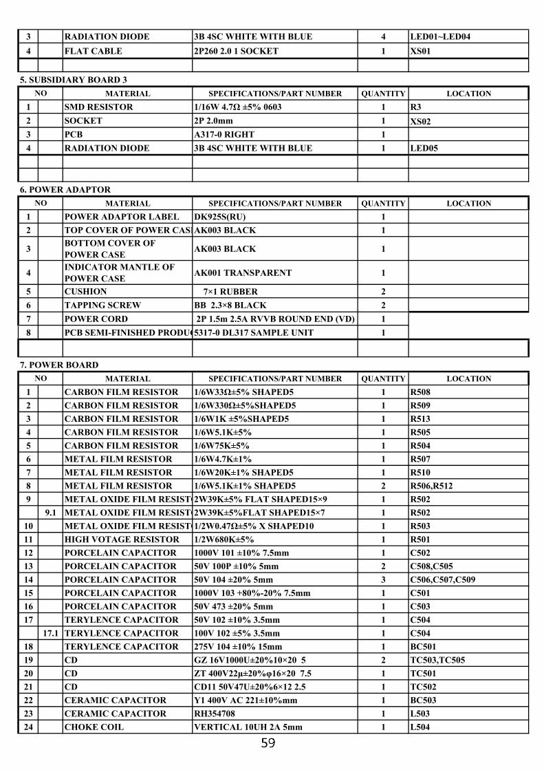
3 RADIATION DIODE 3B 4SC WHITE WITH BLUE 4 LED01~LED044 FLAT CABLE 2P260 2.0 1 SOCKET 1 XS01
5. SUBSIDIARY BOARD 3MATERIAL SPECIFICATIONS/PART NUMBER QUANTITY LOCATION
1 SMD RESISTOR 1/16W 4.7Ω ±5% 0603 1 R32 SOCKET 2P 2.0mm 1 XS023 PCB A317-0 RIGHT 14 RADIATION DIODE 3B 4SC WHITE WITH BLUE 1 LED05
6. POWER ADAPTORMATERIAL SPECIFICATIONS/PART NUMBER QUANTITY LOCATION
1 POWER ADAPTOR LABEL DK925S(RU) 12 TOP COVER OF POWER CASEAK003 BLACK 1
3 BOTTOM COVER OFPOWER CASE AK003 BLACK 1
4 INDICATOR MANTLE OFPOWER CASE AK001 TRANSPARENT 1
5 CUSHION φ7×1 RUBBER 26 TAPPING SCREW BB 2.3×8 BLACK 27 POWER CORD 2P 1.5m 2.5A RVVB ROUND END (VD) 18 PCB SEMI-FINISHED PRODUC5317-0 DL317 SAMPLE UNIT 1
7. POWER BOARDMATERIAL SPECIFICATIONS/PART NUMBER QUANTITY LOCATION
1 CARBON FILM RESISTOR 1/6W33Ω±5% SHAPED5 1 R5082 CARBON FILM RESISTOR 1/6W330Ω±5%SHAPED5 1 R5093 CARBON FILM RESISTOR 1/6W1K ±5%SHAPED5 1 R5134 CARBON FILM RESISTOR 1/6W5.1K±5% 1 R5055 CARBON FILM RESISTOR 1/6W75K±5% 1 R5046 METAL FILM RESISTOR 1/6W4.7K±1% 1 R5077 METAL FILM RESISTOR 1/6W20K±1% SHAPED5 1 R5108 METAL FILM RESISTOR 1/6W5.1K±1% SHAPED5 2 R506,R5129 METAL OXIDE FILM RESISTO2W39K±5% FLAT SHAPED15×9 1 R502
9.1 METAL OXIDE FILM RESISTO2W39K±5%FLAT SHAPED15×7 1 R50210 METAL OXIDE FILM RESISTO1/2W0.47Ω±5% X SHAPED10 1 R50311 HIGH VOTAGE RESISTOR 1/2W680K±5% 1 R50112 PORCELAIN CAPACITOR 1000V 101 ±10% 7.5mm 1 C50213 PORCELAIN CAPACITOR 50V 100P ±10% 5mm 2 C508,C50514 PORCELAIN CAPACITOR 50V 104 ±20% 5mm 3 C506,C507,C50915 PORCELAIN CAPACITOR 1000V 103 +80%-20% 7.5mm 1 C50116 PORCELAIN CAPACITOR 50V 473 ±20% 5mm 1 C50317 TERYLENCE CAPACITOR 50V 102 ±10% 3.5mm 1 C504
17.1 TERYLENCE CAPACITOR 100V 102 ±5% 3.5mm 1 C50418 TERYLENCE CAPACITOR 275V 104 ±10% 15mm 1 BC50119 CD GZ 16V1000U±20%10×20 5 2 TC503,TC50520 CD ZT 400V22µ±20%φ16×20 7.5 1 TC50121 CD CD11 50V47U±20%6×12 2.5 1 TC50222 CERAMIC CAPACITOR Y1 400V AC 221±10%mm 1 BC50323 CERAMIC CAPACITOR RH354708 1 L50324 CHOKE COIL VERTICAL 10UH 2A 5mm 1 L504
NO
NO
NO
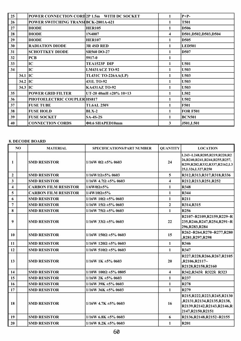
25 POWER CONNECTION CORD2P 1.5m WITH DC SOCKET 1 P+P-26 POWER SWITCHING TRANSFBCK-2801A-621 1 T50127 DIODE HER105 1 D50628 DIODE 1N4007 4 D501,D502,D503,D50429 DIODE HER107 1 D50530 RADIATION DIODE 3R 4SD RED 1 LED50131 SCHOTTKEY DIODE SR560 DO-27 1 D50732 PCB 5917-0 133 IC TEA1523P DIP 1 U50134 IC LM431ACZ TO-92 1 U503
34.1 IC TL431C TO-226AA(LP) 1 U50334.2 IC 431L TO-92 1 U50334.3 IC KA431AZ TO-92 1 U503
35 POWER GRID FILTER UT-20 40mH ±20% 10×13 1 L50236 PHOTOELECTRIC COUPLER HS817 1 U50237 FUSE TUBE T1.6AL 250V 1 F50138 FUSE HOLD BLX-2 1 FOR F50139 FUSE SOCKET SA-4S-2S 1 BCN50140 CONNECTION CORDS Φ0.6 SHAPED10mm 3 J501,L501
8. DECODE BOARD
MATERIAL SPECIFICATIONS/PART NUMBER QUANTITY LOCATION
1 SMD RESISTOR 1/16W 0Ω ±5% 0603 24
L243~L248,R205,R219,R220,R226,R240,R241,R244,R255,R257,R259,R282,R332,R337,R2162,L325,L326,L327,R250
2 SMD RESISTOR 1/16W1Ω±5% 0603 5 R312,R313,R317,R318,R3363 SMD RESISTOR 1/16W 4.7Ω ±5% 0603 4 R212,R213,R251,R2524 CARBON FILM RESISTOR 1/6W0Ω±5% 1 R3485 CARBON FILM RESISTOR 1/4W10Ω±5% 1 R3446 SMD RESISTOR 1/16W 10Ω ±5% 0603 1 R2117 SMD RESISTOR 1/16W 15Ω ±5% 0603 2 R314,R3158 SMD RESISTOR 1/16W 75Ω ±5% 0603 1 R256
9 SMD RESISTOR 1/16W 33Ω ±5% 0603 22R2107~R2109,R2159,R229~R235,R246,R247,R254,R291~R296,R283,R284
10 SMD RESISTOR 1/16W 150Ω ±5% 0603 15 R262~R264,R270~R277,R280,R281,R297,R298
11 SMD RESISTOR 1/16W 120Ω ±5% 0603 1 R34612 SMD RESISTOR 1/16W 510Ω ±5% 0603 1 R347
13 SMD RESISTOR 1/16W 1K ±5% 0603 20R227,R228,R266,R267,R2105,R2106,R2117~R2128,R2158,R2160
14 SMD RESISTOR 1/10W 100Ω ±5% 0805 4 R342,R343,R322,R32315 SMD RESISTOR 1/16W 2K ±5% 0603 1 R23716 SMD RESISTOR 1/16W 39K ±5% 0603 1 R27817 SMD RESISTOR 1/16W 36K ±5% 0603 1 R279
18 SMD RESISTOR 1/16W 4.7K ±5% 0603 16
R215,R222,R223,R245,R2130,R2131,R2134,R2135,R2138,R2139,R2142,R2143,R2146,R2147,R2150,R2151
19 SMD RESISTOR 1/16W 6.8K ±5% 0603 6 R2136,R2148,R2152~R215520 SMD RESISTOR 1/16W 8.2K ±5% 0603 1 R201
NO
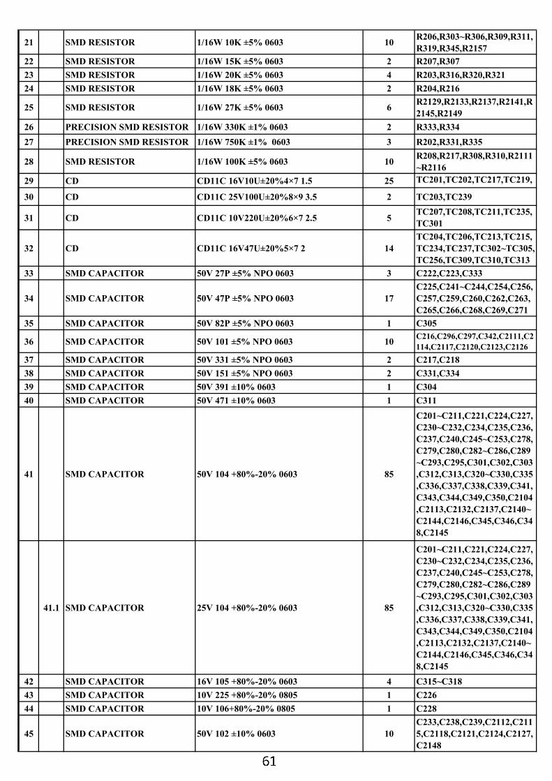
21 SMD RESISTOR 1/16W 10K ±5% 0603 10 R206,R303~R306,R309,R311,R319,R345,R2157
22 SMD RESISTOR 1/16W 15K ±5% 0603 2 R207,R30723 SMD RESISTOR 1/16W 20K ±5% 0603 4 R203,R316,R320,R32124 SMD RESISTOR 1/16W 18K ±5% 0603 2 R204,R216
25 SMD RESISTOR 1/16W 27K ±5% 0603 6 R2129,R2133,R2137,R2141,R2145,R2149
26 PRECISION SMD RESISTOR 1/16W 330K ±1% 0603 2 R333,R33427 PRECISION SMD RESISTOR 1/16W 750K ±1% 0603 3 R202,R331,R335
28 SMD RESISTOR 1/16W 100K ±5% 0603 10 R208,R217,R308,R310,R2111~R2116
29 CD CD11C 16V10U±20%4×7 1.5 25 TC201,TC202,TC217,TC219,
30 CD CD11C 25V100U±20%8×9 3.5 2 TC203,TC239
31 CD CD11C 10V220U±20%6×7 2.5 5TC207,TC208,TC211,TC235,TC301
32 CD CD11C 16V47U±20%5×7 2 14TC204,TC206,TC213,TC215,TC234,TC237,TC302~TC305,TC256,TC309,TC310,TC313
33 SMD CAPACITOR 50V 27P ±5% NPO 0603 3 C222,C223,C333
34 SMD CAPACITOR 50V 47P ±5% NPO 0603 17C225,C241~C244,C254,C256,C257,C259,C260,C262,C263,C265,C266,C268,C269,C271
35 SMD CAPACITOR 50V 82P ±5% NPO 0603 1 C305
36 SMD CAPACITOR 50V 101 ±5% NPO 0603 10 C216,C296,C297,C342,C2111,C2114,C2117,C2120,C2123,C2126
37 SMD CAPACITOR 50V 331 ±5% NPO 0603 2 C217,C21838 SMD CAPACITOR 50V 151 ±5% NPO 0603 2 C331,C33439 SMD CAPACITOR 50V 391 ±10% 0603 1 C30440 SMD CAPACITOR 50V 471 ±10% 0603 1 C311
41 SMD CAPACITOR 50V 104 +80%-20% 0603 85
C201~C211,C221,C224,C227,C230~C232,C234,C235,C236,C237,C240,C245~C253,C278,C279,C280,C282~C286,C289~C293,C295,C301,C302,C303,C312,C313,C320~C330,C335,C336,C337,C338,C339,C341,C343,C344,C349,C350,C2104,C2113,C2132,C2137,C2140~C2144,C2146,C345,C346,C348,C2145
41.1 SMD CAPACITOR 25V 104 +80%-20% 0603 85
C201~C211,C221,C224,C227,C230~C232,C234,C235,C236,C237,C240,C245~C253,C278,C279,C280,C282~C286,C289~C293,C295,C301,C302,C303,C312,C313,C320~C330,C335,C336,C337,C338,C339,C341,C343,C344,C349,C350,C2104,C2113,C2132,C2137,C2140~C2144,C2146,C345,C346,C348,C2145
42 SMD CAPACITOR 16V 105 +80%-20% 0603 4 C315~C31843 SMD CAPACITOR 10V 225 +80%-20% 0805 1 C22644 SMD CAPACITOR 10V 106+80%-20% 0805 1 C228
45 SMD CAPACITOR 50V 102 ±10% 0603 10C233,C238,C239,C2112,C2115,C2118,C2121,C2124,C2127,C2148
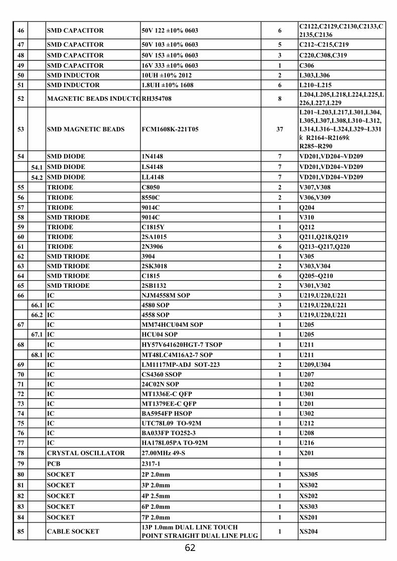
46 SMD CAPACITOR 50V 122 ±10% 0603 6 C2122,C2129,C2130,C2133,C2135,C2136
47 SMD CAPACITOR 50V 103 ±10% 0603 5 C212~C215,C21948 SMD CAPACITOR 50V 153 ±10% 0603 3 C220,C308,C31949 SMD CAPACITOR 16V 333 ±10% 0603 1 C30650 SMD INDUCTOR 10UH ±10% 2012 2 L303,L30651 SMD INDUCTOR 1.8UH ±10% 1608 6 L210~L215
52 MAGNETIC BEADS INDUCTORH354708 8 L204,L205,L218,L224,L225,L226,L227,L229
53 SMD MAGNETIC BEADS FCM1608K-221T05 37
L201~L203,L217,L301,L304,L305,L307,L308,L310~L312,L314,L316~L324,L329~L331,R2164~R2169,R285~R290
54 SMD DIODE 1N4148 7 VD201,VD204~VD209
54.1 SMD DIODE LS4148 7 VD201,VD204~VD20954.2 SMD DIODE LL4148 7 VD201,VD204~VD209
55 TRIODE C8050 2 V307,V30856 TRIODE 8550C 2 V306,V30957 TRIODE 9014C 1 Q20458 SMD TRIODE 9014C 1 V31059 TRIODE C1815Y 1 Q21260 TRIODE 2SA1015 3 Q211,Q218,Q21961 TRIODE 2N3906 6 Q213~Q217,Q22062 SMD TRIODE 3904 1 V30563 SMD TRIODE 2SK3018 2 V303,V30464 SMD TRIODE C1815 6 Q205~Q21065 SMD TRIODE 2SB1132 2 V301,V30266 IC NJM4558M SOP 3 U219,U220,U221
66.1 IC 4580 SOP 3 U219,U220,U22166.2 IC 4558 SOP 3 U219,U220,U221
67 IC MM74HCU04M SOP 1 U20567.1 IC HCU04 SOP 1 U205
68 IC HY57V641620HGT-7 TSOP 1 U21168.1 IC MT48LC4M16A2-7 SOP 1 U211
69 IC LM1117MP-ADJ SOT-223 2 U209,U30470 IC CS4360 SSOP 1 U20771 IC 24C02N SOP 1 U20272 IC MT1336E-C QFP 1 U30173 IC MT1379EE-C QFP 1 U20174 IC BA5954FP HSOP 1 U30275 IC UTC78L09 TO-92M 1 U21276 IC BA033FP TO252-3 1 U20877 IC HA178L05PA TO-92M 1 U21678 CRYSTAL OSCILLATOR 27.00MHz 49-S 1 X20179 PCB 2317-1 180 SOCKET 2P 2.0mm 1 XS30581 SOCKET 3P 2.0mm 1 XS30282 SOCKET 4P 2.5mm 1 XS20283 SOCKET 6P 2.0mm 1 XS30384 SOCKET 7P 2.0mm 1 XS201
85 CABLE SOCKET 13P 1.0mm DUAL LINE TOUCHPOINT STRAIGHT DUAL LINE PLUG 1 XS204

86 CABLE SOCKET 24P 0.5mm SMD WITH CLASP 1 XS301


![COVER ILLUSTRATION Photography: “Mapparium Eastern ...€¦ · COVER ILLUSTRATION Photography: “Mapparium Eastern Hemisphere [front]”, by Boston Public Library @flickr, licensed](https://img.pdfslide.us/doc/110x75/6001ce2cf0a1ca1dee40f301/cover-illustration-photography-aoemapparium-eastern-cover-illustration-photography.jpg)